1
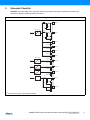
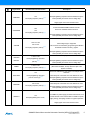
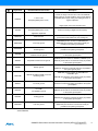
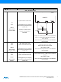
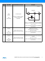
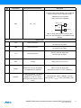
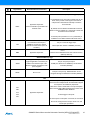
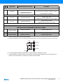
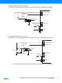
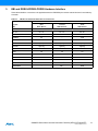
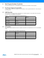
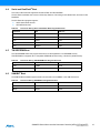
Application Note SAMA5D3 Series Microcontroller Schematic Checklist ARM-based Embedded MPU Scope This application note is a schematic review checklist for systems embedding the Atmel® ARM®-based SAMA5D3 series embedded MPU. It provides the user with the requirements regarding the different pin connections that must be considered before starting any new board design. The application note also describes the minimum hardware resources required to quickly develop an application with the SAMA5D3. It does not consider PCB layout constraints. It also provides recommendations regarding low-power design constraints to minimize power consumption. This application note is not intended to be exhaustive. Its objective is to cover as many configurations of use as possible. The checklist contains a column for use by designers, making it easy to track and verify each line item. 11207B–ATARM–22-Oct-13 Table of Contents Scope . . . . . . . . . . . . . . . . . . . . . . . . . . . . . . . . . . . . . . . . . . . . . . . . . . . . 1 Table of Contents . . . . . . . . . . . . . . . . . . . . . . . . . . . . . . . . . . . . . . . . . . . 2 1. Reference Documents . . . . . . . . . . . . . . . . . . . . . . . . . . . . . . . . . . . . 3 2. Schematic Checklist . . . . . . . . . . . . . . . . . . . . . . . . . . . . . . . . . . . . . 4 3. EBI and DDR2/LPDDR/LPDDR2 Hardware Interface . . . . . . . . . . . 13 4. Boot Program Hardware Constraints . . . . . . . . . . . . . . . . . . . . . . . . 15 4.1 4.2 4.3 4.4 4.5 4.6 Boot Program Supported Crystals (MHz) . . . . . . . . . . . . . . . . . . . . . . . . . . . . 15 NAND Flash Boot . . . . . . . . . . . . . . . . . . . . . . . . . . . . . . . . . . . . . . . . . . . . . . 15 SD Card Boot . . . . . . . . . . . . . . . . . . . . . . . . . . . . . . . . . . . . . . . . . . . . . . . . . 15 Serial and DataFlash® Boot. . . . . . . . . . . . . . . . . . . . . . . . . . . . . . . . . . . . . . . 16 TWI EEPROM Boot. . . . . . . . . . . . . . . . . . . . . . . . . . . . . . . . . . . . . . . . . . . . . 16 SAM-BA® Boot . . . . . . . . . . . . . . . . . . . . . . . . . . . . . . . . . . . . . . . . . . . . . . . . 16 5. Revision History . . . . . . . . . . . . . . . . . . . . . . . . . . . . . . . . . . . . . . . . 17 SAMA5D3 Series Microcontroller Schematic Checklist [APPLICATION NOTE] 11207B–ATARM–22-Oct-13 2 1. Reference Documents Before starting to work with this application note, it is strongly recommended to check the latest documents available for the SAMA5D3 devices on the Atmel web site. Table 1-1 gives the document titles that provide additional information to support this application note. Table 1-1. Reference Documents Information Document Title User Manual Electrical/Mechanical Characteristics Ordering Information SAMA5D3 Series Datasheet Errata Internal Architecture of Processor ARM/Thumb Instruction Sets Cortex-A5 Technical Reference Manual Embedded In-circuit Emulator Evaluation Kit User Guide SAMA5D3 Series Evaluation Kit User Guide SAMA5D3 Series Microcontroller Schematic Checklist [APPLICATION NOTE] 11207B–ATARM–22-Oct-13 3 2. Schematic Checklist CAUTION: The board design must comply with power-up and power down sequence guidelines provided in the datasheet to guarantee reliable operation of the device. 1.2V, 1.8V, 2.5V, 3.3V Power Supplies Schematic Example(1) 0µ VDDOSC 1R 100nF 4.7µF LDO Converter 10µH GNDOSC VDDANA 3.3V 1R 100nF 4.7µF GNDANA VDDBU 100nF GNDBU VDDIOP0,1 100nF GNDIOP VDDUTMII 100nF GNDUTMI VDDIOM 100nF LDO Converter GNDIOM VDDFUSE 100nF 2.5V GNDFUSE DC/DC Converter VDDIODDR 100nF 1.8V GNDIODDR DC/DC Converter VDDCORE 100nF 1.2V GNDCORE LDO Converter 10µH VDDPLLA 1.2V 1R 100nF 4.7µF GNDPLL VDDUTMIC 2.2µF 100nF GNDUTMI (1) These values are given only as a typical example SAMA5D3 Series Microcontroller Schematic Checklist [APPLICATION NOTE] 11207B–ATARM–22-Oct-13 4 Signal Name Recommended Pin Connection Description Powers the device. VDDCORE 1.2V Decoupling capacitor (100 nF) (1)(2) Decoupling/filtering capacitors must be added to improve start-up stability and reduce source voltage drop. Supply ripple must not exceed 20 mVrms. Powers the DDR2/LPDDR Interface I/O lines. 1.8V VDDIODDR Powers the LPDDR2 Interface I/O lines. 1.2V Decoupling capacitor (100 nF)(1)(2) Decoupling/filtering capacitors must be added to improve start-up stability and reduce source voltage drop. Powers the External Memory Interface I/O lines. VDDIOM 1.65V to 1.95V Dual voltage range is supported. 3.0V to 3.6V The I/O drives are selected by programming the DRIVE0 and DRIVE1 fields in the SFR_ register. Decoupling capacitor (100 nF)(1)(2) Decoupling/filtering capacitors must be added to improve start-up stability and reduce source voltage drop. VDDIOP0 VDDIOP1 VDDBU Powers the peripheral I/O lines. 1.65V to 3.6V Decoupling/filtering capacitors Decoupling/filtering capacitors must be added to improve start-up stability and reduce source voltage drop. (100 nF)(1)(2) Powers the Backup unit. 1.65V to 3.6V Decoupling capacitor (100 nF)(1)(2) Powers the USB device, host UTMI+ core and part of the UTMI PLL. 1.2V VDDUTMIC Decoupling/filtering capacitors (100 nF and 2.2 µF) (Slow Clock Oscillator, On-chip RC and a part of the System Controller). (1)(2) Must always be connected even if the USB is not used. Decoupling/filtering capacitors must be added to improve start-up stability and reduce source voltage drop. Powers the USB device and host UTMI+ interface. VDDUTMII 3.0V to 3.6V Must always be connected even if the USB is not used. Decoupling capacitor (100 nF)(1)(2) Decoupling/filtering capacitors must be added to improve start-up stability and reduce source voltage drop. Powers the PLLA cell. VDDPLLA 1.2V Decoupling/filtering RLC circuit(1) The VDDPLLA power supply pin draws small current, but it is noise sensitive. Care must be taken in VDDPLLA power supply routing, decoupling and also on bypass capacitors. Supply ripple must not exceed 10 mVrms. SAMA5D3 Series Microcontroller Schematic Checklist [APPLICATION NOTE] 11207B–ATARM–22-Oct-13 5 Signal Name VDDOSC Recommended Pin Connection 1.65V to 3.6V Decoupling/filtering RLC circuit(1) Description Powers the main oscillator cell and PLL UTMI. If PLL UTMI is used, the range is to be 3.0V to 3.6V. The VDDOSC power supply pin is noise-sensitive. Care must be taken in VDDOSC power supply routing, decoupling and also on bypass capacitors. Supply ripple must not exceed 30 mVrms. 3.0V to 3.6V VDDANA Decoupling/filtering RLC circuit(1) Powers the Analog to Digital Converter (ADC). Application-dependent VDDFUSE 2.25V to 2.75V Powers the fuse box for Programming. It can be tied to ground with a 100Ω resistor for fuse reading only. GNDCORE pins are common to VDDCORE pins. GNDCORE GNDIODDR GNDIOM Core Chip ground GNDCORE pins should be connected as shortly as possible to the system ground plane. DDR/LPDDR/LPDDR2 interface GNDIODDR pins should be connected as shortly as possible to the system ground plane. I/O lines ground NAND and SMC Interface I/O lines ground GNDIOM pins should be connected as shortly as possible to the system ground plane. GNDIOP pins are common to VDDIOP0, VDDIOP1 pins. GNDIOP Peripherals and ISI I/O lines ground GNDBU Backup ground GNDUTMI UDPHS and UHPHS UTMI+ Core and interface ground GNDPLL PLLA cell ground GNDIOP pins should be connected as shortly as possible to the system ground plane. GNDBU pin is provided for VDDBU pins. GNDOSC PLLUTMI and Oscillator ground GNDBU pin should be connected as shortly as possible to the system ground plane. GNDUTMI pins are common to VDDUTMII and VDDUTMIC pins. GNDUTMI pins should be connected as shortly as possible to the system ground plane. GNDPLL pin is provided for VDDPLLA pin. GNDPLL pin should be connected as shortly as possible to the system ground plane. GNDOSC pin is provided for VDDOSC pin. GNDOSC pin should be connected as shortly as possible to the system ground plane. GNDANA pins are common to VDDANA pins. GNDANA Analog ground GNDANA pins should be connected as shortly as possible to the system ground plane. GNDFUSE pins are common to VDDFUSE pins. GNDFUSE Note: Fuse box ground GNDFUSE pins should be connected as shortly as possible to the system ground plane. For more information please refer to the Core Power Supply POR Characteristics section of the SAMA5D3 series datasheet. SAMA5D3 Series Microcontroller Schematic Checklist [APPLICATION NOTE] 11207B–ATARM–22-Oct-13 6 Signal Name Recommended Pin Connection Description Clock, Oscillator and PLL Crystal Load Capacitance to check (CCRYSTAL). SAMA5D3 XIN XOUT GNDOSC Crystals between 8 and 16 MHz XIN XOUT 12 MHz Main Oscillator in Normal Mode USB High Speed (not Full Speed) Host and Device peripherals need a 12 MHz clock. Capacitors on XIN and XOUT (Crystal Load Capacitance dependent) CCRYSTAL CLEXT CLEXT Example: for a 12 MHz crystal with a load capacitance of CCRYSTAL = 15 pF, external capacitors are required: CLEXT = 20 pF. Refer to the electrical specifications of the SAMA5D3 series datasheet. XIN XIN: external clock source XOUT XOUT: can be left unconnected 12 MHz USB High speed (not Full Speed) Main Oscillator in Bypass Mode Host and Device peripherals need a 12 MHz clock. XIN XIN: can be left unconnected XOUT XOUT: can be left unconnected 12 MHz USB High Speed (not Full Speed) Main Oscillator Host and Device peripherals need a 12 MHz clock. Disabled VDDOSC square wave signal External clock source up to 50 MHz Duty Cycle: 40 to 60% Refer to the electrical specifications of the SAMA5D3 series datasheet. Typical nominal frequency 12 MHz (Internal 12 MHz RC Oscillator) Duty Cycle: 45 to 55% Refer to the electrical specifications of the SAMA5D3 series datasheet. SAMA5D3 Series Microcontroller Schematic Checklist [APPLICATION NOTE] 11207B–ATARM–22-Oct-13 7 Signal Name Recommended Pin Connection Description Crystal load capacitance to check (CCRYSTAL32). SAMA5D3 XIN32 XIN32 XOUT32 GNDBU 32.768 kHz Crystal C CRYSTAL32 XOUT32 Capacitors on XIN32 and XOUT32 Slow Clock Oscillator (Crystal Load Capacitance dependent) CLEXT32 CLEXT32 Example: for a 32.768 kHz crystal with a load capacitance of CCRYSTAL32 = 12.5 pF, external capacitors are required: CLEXT32 = 19 pF. Refer to the electrical specifications of the SAMA5D3 series datasheet. XIN32 VDDBU square wave signal XOUT32 XIN32: external clock source Slow XOUT32: can be left unconnected External clock source up to 44 kHz Duty Cycle: 40 to 60% Refer to the electrical specifications of the SAMA5D3 series datasheet. Clock Oscillator in Bypass Mode XIN32 XOUT32 XIN32: can be left unconnected Slow Clock Oscillator XOUT32: can be left unconnected Typical nominal frequency 32 kHz (internal 32 kHz RC oscillator) Duty Cycle: 45 to 55% Refer to the electrical specifications of the SAMA5D3 series datasheet. Disabled SAMA5D3 Series Microcontroller Schematic Checklist [APPLICATION NOTE] 11207B–ATARM–22-Oct-13 8 Signal Name Recommended Pin Connection Description Bias Voltage Reference for USB To reduce as much as possible the noise on VBG pin please check the Layout consideration below: - VBG path as short as possible - ground connection to GNDUTMI VBG 0.9 - 1.1V(5) 5K62 ± 1% Ω VBG 10 pF GNDUTMI VBG can be left unconnected if USB is not used. Refer to the signal description of the SAMA5D3 series datasheet. ICE and JTAG(3) This pin is a Schmitt trigger input. TCK Pull-up (100 kOhm)(1) TMS Pull-up (100 kOhm)(1) TDI Pull-up (100 kOhm)(1) TDO Floating Output driven at up to VVDDIOP0 NTRST Please refer to the pin description of the SAMA5D3 series datasheet. This pin is a Schmitt trigger input. JTAGSEL In harsh environments(4), it is strongly recommended to tie this pin to GNDBU if not used or to add an external low-value resistor (such as 1 kOhm). No internal pull-up resistor. This pin is a Schmitt trigger input. No internal pull-up resistor. This pin is a Schmitt trigger input. No internal pull-up resistor. Internal pull-up resistor to VVDDIOP0 (100 kOhm). Internal pull-down resistor to GNDBU (15 kOhm). Must be tied to VVDDBU to enter JTAG Boundary Scan. SAMA5D3 Series Microcontroller Schematic Checklist [APPLICATION NOTE] 11207B–ATARM–22-Oct-13 9 Signal Name Recommended Pin Connection Description Reset/Test NRST is a bidirectional pin (Schmitt trigger input). It is handled by the on-chip reset controller and can be driven low to provide a reset signal to the external components or asserted low externally to reset the microcontroller. Application dependent. NRST Can be connected to a push button for hardware reset. By default, the User Reset is enabled after a General Reset so that it is possible for a component to assert low and reset the microcontroller. An internal pull-up resistor to VVDDIOP0 (100 kOhm) is available for User Reset and External Reset control. TST In harsh environments(4), it is strongly recommended to tie this pin to GNDBU if not used or to add an external low-value resistor (such as 10 kOhm). BMS Application dependent. This pin is a Schmitt trigger input. Internal pull-down resistor to GNDBU (15 kOhm). Must be tied to VVDDIOP0 to boot from Embedded ROM. Must be tied to GNDIOP to boot from external memory (EBI Chip Select 0). Shutdown/Wake-up Logic Application dependent. SHDN WKUP This pin is a push-pull output. A typical application connects the pin SHDN to the shutdown input of the DC/DC Converter providing the main power supplies. SHDN pin is driven low to GNDBU by the Shutdown Controller (SHDWC). 0V to VVDDBU This pin is an input-only. WKUP behavior can be configured through the Shutdown Controller (SHDWC). PIO All PIOs are pulled-up inputs (100 kOhm) at reset except those which are multiplexed with the Address Bus signals that require to be enabled as peripherals: Refer to the column “Reset State” of the pin description table in the 324-ball LFBGA package pinout section of the SAMA5D3 series datasheet. PAx PBx PCx PDx Application dependent. Schmitt trigger on all inputs. PEx To reduce power consumption if not used, the concerned PIO can be configured as an output, driven at ‘0’ with internal pull-up disabled. SAMA5D3 Series Microcontroller Schematic Checklist [APPLICATION NOTE] 11207B–ATARM–22-Oct-13 10 Signal Name Recommended Pin Connection Description ADC TSADVREF 3.3V to VDDANA ADVREF is a pure analog input. Decoupling/filtering capacitors Application dependent. To reduce power consumption, if ADC is not used: connect ADVREF to GNDANA. EBI D0 - D15 Application dependent. A0 - A25 Application dependent. Data Bus (D0 to D15) All data lines are pull-up inputs to VVDDIOM at reset. Address Bus (A0 to A25) All address lines are driven to ‘0’ at reset. HSMC - DDR2/LPDDR/LPDDR2 Controller - NAND Flash Support See “EBI and DDR2/LPDDR/LPDDR2 Hardware Interface” on page 13. USB High Speed Host (UHPHS)/USB High Speed Device (UDPHS) HHSDPA/DHSDP HHSDMA/DHSDM HHSDPB/HHSDMB HHSDPC/HHSDMC Application dependent(5). Pull-down output at reset. Application dependent(5). Pull-down output at reset. (5) Application dependent . Pull-down output at reset. Notes: 1. These values are given only as a typical example. 2. Decoupling capacitors must be connected as close as possible to the microcontroller and on each concerned pin. 100nF VDDCORE 100nF VDDCORE 100nF VDDCORE GND 3. It is recommended to establish accessibility to a JTAG connector for debug in any case. 4. In a well-shielded environment subject to low magnetic and electric field interference, the pin may be left unconnected. In noisy environments, a connection to ground is recommended. SAMA5D3 Series Microcontroller Schematic Checklist [APPLICATION NOTE] 11207B–ATARM–22-Oct-13 11 5. Example of USB High Speed Host connection: More details are in the USB Host High Speed Port (UHPHS) section of the SAMA5D3 series datasheet. PIO (VBUS ENABLE) "A" Receptacle 1 = VBUS 2 = D3 = D+ 4 = GND +5V HHSDM/HFSDM 3 4 Shell = Shield 1 2 HHSDP/HFSDP 5K62 ± 1% Ω VBG 10 pF GNDUTMI 6. Typical USB High Speed Device connection: More details are in the USB High Speed Device Port (UDPHS) section of the SAMA5D3 series datasheet. PIO (VBUS DETECT) 15k Ω (1) "B" Receptacle 1 = VBUS 2 = D3 = D+ 4 = GND 1 2 3 4 DHSDM/DFSDM Shell = Shield (1) 22k Ω CRPB CRPB:1µF to 10µF DHSDP/DFSDP 5K62 ± 1%Ω VBG 10 pF GNDUTMI (1) The values shown on the 22 kΩ and 15 kΩ resistors are only valid with 3.3V supplied PIOs. SAMA5D3 Series Microcontroller Schematic Checklist [APPLICATION NOTE] 11207B–ATARM–22-Oct-13 12 3. EBI and DDR2/LPDDR/LPDDR2 Hardware Interface These tables detail the connections to be applied between the EBI/DDR2 pins and the external devices for each Memory Controller. Table 3-1. EBI Pins and External Static Devices Connections Pins of the Interfaced Device 8-bit Static Device Signals: EBI_ Controller 2 x 8-bit Static Devices 16-bit Static Device SMC D0 - D7 D0 - D7 D0 - D7 D0 - D7 D8 - D15 – D8 - D15 D8 - D15 A0/NBS0 A0 – NLB A1 A1 A0 A0 A2-A22 A[2:22] A[1:21] A[1:21] A23-A25 A[23:25] A[22:24] A[22:24] NCS0 CS CS CS NCS1 CS CS CS NCS2 CS CS CS NCS3/NANDCS CS CS CS NRD/NANDOE OE OE OE NWE/NWR0/NANDWE NWR1/NBS1 Notes: 1. WE – (1) WE (1) NUB WE WE NWR0 enables lower byte writes. NWR1 enables upper byte writes. SAMA5D3 Series Microcontroller Schematic Checklist [APPLICATION NOTE] 11207B–ATARM–22-Oct-13 13 Table 3-2. EBI Pins and External Device Connections Pins of the Interfaced Device Signals: EBI_ 8-bit NAND Flash Controller 16-bit NAND Flash NFC D0 - D7 NFD0 - NFD7 NFD0 - NFD7 D8 - D15 – NFD8 - NFD15 A21/NANDALE ALE ALE A22/NANDCLE CLE CLE NRD/NANDOE RE RE NWE/NWR0/NANDWE WE WE NCS3/NANDCS CE CE R/B# R/B# A0/NBS0 – – A1 - A20 – – A23 - A25 – – NWR1/NBS1 – – NCS0 – – NCS1 – – NCS2 – – NWAIT – – NANDRDY Table 3-3. DDR2 I/O Lines Usage vs Operating Modes Signal Name DDR2 Mode LPDDR2 Mode LPDDR DDR_VREF VDDIODDR/2 VDDIODDR/2 VDDIODDR/2 DDR_CALP GND via 200Ω resistor GND via 240Ω resistor GND via 200Ω resistor DDR_CALN VDDIODDR via 200Ω resistor VDDIODDR via 240Ω resistor VDDIODDR via 200Ω resistor DDR_CK, DDR_CKN CLK and CLKN CLK and CLKN CLK and CLKN DDR_CKE CLKE CLKE CLKE DDR_CS CS CS CS DDR_BA[2..0] BA[2..0] BA[2..0] BA[2..0] DDR_WE WE CA2 WE DDR_RAS - DDR_CAS RAS, CAS CA0, CA1 RAS, CAS DDR_A[13..0] A[13:0] CAx, with x>2 A[13:0] DDR_D[31..0] D[31:0] D[31:0] D[31:0] DQS[3..0], DQSN[3..0] DQS[3:0] DQSN connected to DDR_VREF DQS[3:0] DQSN[3:0] DQS[3:0] DQSN connected to DDR_VREF DQM[3..0] DQM[3..0] DQM[3..0] DQM[3..0] SAMA5D3 Series Microcontroller Schematic Checklist [APPLICATION NOTE] 11207B–ATARM–22-Oct-13 14 4. Boot Program Hardware Constraints See the Boot Strategies section of the SAMA5D3 series datasheet for more details on the boot program. 4.1 Boot Program Supported Crystals (MHz) A 12 MHz crystal or external clock (in bypass mode) is mandatory in order to generate USB and PLL clocks correctly for the following boots. 4.2 NAND Flash Boot Boot is possible if the first page contains a valid header or if it is ONFI compliant. For more details, refer to the section Nand Flash Boot of the SAMA5D3 series datasheet. Table 4-1. 4.3 Pins Driven during NAND Flash Boot Program Execution Peripheral Pin PIO Line EBI CS3 SMC NANDOE – EBI CS3 SMC NANDWE – EBI CS3 SMC NANDCS – EBI CS3 SMC NAND ALE – EBI CS3 SMC NAND CLE – EBI CS3 SMC Cmd/Addr/Data – SD Card Boot SD Card Boot supports all SD Card memories compliant with SD Memory Card Specification V2.0. This includes SDHC cards. Table 4-2. Pins Driven During SD Card Boot Program Execution Peripheral Pin PIO Line MCI0 MCI0_CK PD9 MCI0 MCI0_D0 PD1 MCI0 MCI0_D1 PD2 MCI0 MCI0_D2 PD3 MCI0 MCI0_D3 PD4 SAMA5D3 Series Microcontroller Schematic Checklist [APPLICATION NOTE] 11207B–ATARM–22-Oct-13 15 4.4 Serial and DataFlash® Boot Two kinds of SPI Flash are supported: SPI Serial Flash and SPI DataFlash. The SPI Flash bootloader tries to boot on SPI0 Chip Select 0, first looking for SPI Serial Flash, and then for SPI DataFlash. The SPI Flash Boot program supports: All SPI Serial Flash devices All DataFlash devices Table 4-3. 4.5 Pins Driven During Serial or DataFlash Boot Program Execution Peripheral Pin PIO Line SPI0 MOSI PD11 SPI0 MISO PD10 SPI0 SPCK PD12 SPI0 NPCS0 PD13 SPI0 NPCS1 PD14 TWI EEPROM Boot The TWI EEPROM Flash boot program searches for a valid application in an EEPROM memory. TWI EEPROM boot supports all I2C-compatible EEPROM memories using 7-bit device (Address 0x50). Table 4-4. 4.6 Pins Driven During TWI EEPROM Boot Program Execution Peripheral Pin PIO Line TWI0 TWD0 PA30 TWI0 TWCK0 PA31 SAM-BA® Boot The SAM-BA Boot Assistant supports serial communication via the DBGU or the USB Device Port. Table 4-5. Pins Driven During SAM-BA Boot Program Execution Peripheral Pin PIO Line DBGU DRXD PB30 DBGU DTXD PB31 SAMA5D3 Series Microcontroller Schematic Checklist [APPLICATION NOTE] 11207B–ATARM–22-Oct-13 16 5. Revision History Doc. Rev Change Request Ref. Comments 9386 Modified voltage range for “VDDIOM” and “VDDBU” on page 5. Modified details of I/O selection in description of “VDDIOM” and removed information on high drive mode selection for 3.3V memories. 11207B rfo In description of “VDDBU”, removed information on supply ripple. rfo “VDDUTMII”: updated description with USB information. 8523 “VDDUTMIC”: updated description with USB information. rfo, 8523 In description of “VDDOSC”, updated first line on powering the main oscillator cell and added detail on PLL UTMI use. Removed ‘draws small current’. rfo “VBG”: updated description with USB information. 8523 Removed references to PLLA and VDDPLLA for “GNDOSC”. rfo Corrected typo in description of “TSADVREF”. rfo Changed graphics for notes (5) and (6) on page 12. Removed comments (1) and (2) below note (6) and removed comment (2) below note (6). 9386 Modified all information in Table 3-2 “EBI Pins and External Device Connections”. 9386 Inserted new Table 3-3 “DDR2 I/O Lines Usage vs Operating Modes”. 9386 Table 4-3 “Pins Driven During Serial or DataFlash Boot Program Execution”: Added new row with NPCS1 pin and PD14 PIO line. Doc. Rev Comments 11207A First issue. rfo Change Request Ref. SAMA5D3 Series Microcontroller Schematic Checklist [APPLICATION NOTE] 11207B–ATARM–22-Oct-13 17 Atmel Corporation 1600 Technology Drive Atmel Asia Limited Unit 01-5 & 16, 19F Atmel Munich GmbH Business Campus Atmel Japan G.K. 16F Shin-Osaki Kangyo Bldg San Jose, CA 95110 BEA Tower, Millennium City 5 Parkring 4 1-6-4 Osaki, Shinagawa-ku USA 418 Kwun Tong Road D-85748 Garching b. Munich Tokyo 141-0032 Tel: (+1) (408) 441-0311 Kwun Tong, Kowloon GERMANY JAPAN Fax: (+1) (408) 487-2600 HONG KONG Tel: (+49) 89-31970-0 Tel: (+81) (3) 6417-0300 www.atmel.com Tel: (+852) 2245-6100 Fax: (+49) 89-3194621 Fax: (+81) (3) 6417-0370 Fax: (+852) 2722-1369 © 2013 Atmel Corporation. All rights reserved. / Rev.: 11207B–ATARM–22-Oct-13 Atmel®, Atmel logo and combinations thereof, Enabling Unlimited Possibilities®, SAM-BA® and others are registered trademarks or trademarks of Atmel Corporation or its subsidiaries. ARM® and others are registered trademarks or trademarks of ARM Ltd. Other terms and product names may be trademarks of others. Disclaimer: The information in this document is provided in connection with Atmel products. No license, express or implied, by estoppel or otherwise, to any intellectual property right is granted by this document or in connection with the sale of Atmel products. EXCEPT AS SET FORTH IN THE ATMEL TERMS AND CONDITIONS OF SALES LOCATED ON THE ATMEL WEBSITE, ATMEL ASSUMES NO LIABILITY WHATSOEVER AND DISCLAIMS ANY EXPRESS, IMPLIED OR STATUTORY WARRANTY RELATING TO ITS PRODUCTS INCLUDING, BUT NOT LIMITED TO, THE IMPLIED WARRANTY OF MERCHANTABILITY, FITNESS FOR A PARTICULAR PURPOSE, OR NON-INFRINGEMENT. IN NO EVENT SHALL ATMEL BE LIABLE FOR ANY DIRECT, INDIRECT, CONSEQUENTIAL, PUNITIVE, SPECIAL OR INCIDENTAL DAMAGES (INCLUDING, WITHOUT LIMITATION, DAMAGES FOR LOSS AND PROFITS, BUSINESS INTERRUPTION, OR LOSS OF INFORMATION) ARISING OUT OF THE USE OR INABILITY TO USE THIS DOCUMENT, EVEN IF ATMEL HAS BEEN ADVISED OF THE POSSIBILITY OF SUCH DAMAGES. Atmel makes no representations or warranties with respect to the accuracy or completeness of the contents of this document and reserves the right to make changes to specifications and products descriptions at any time without notice. Atmel does not make any commitment to update the information contained herein. Unless specifically provided otherwise, Atmel products are not suitable for, and shall not be used in, automotive applications. Atmel products are not intended, authorized, or warranted for use as components in applications intended to support or sustain life.