1
Use of Dynamic Test Methods to Reveal Mechanical Properties of Nanomaterials
by
H. S. Tanvir Ahmed, B.S.M.E, M.S.M.E
A Dissertation
In
MECHANICAL ENGINEERING
Submitted to the Graduate Faculty
of Texas Tech University in
Partial Fulfillment of
the Requirements for
the Degree of
DOCTOR OF PHILOSOPHY
Approved
Alan F. Jankowski, Ph.D.
(Chairperson of the Committee)
Jharna Chaudhuri, Ph.D.
Alexander Idesman, Ph.D.
Michelle Pantoya, Ph.D.
Shameem Siddiqui, Ph.D.
Fred Hartmeister
Dean of the Graduate School
December, 2010
© Copyright 2010, H. S. Tanvir Ahmed
Dedicated to my parents, my family and friends.
Texas Tech University, H. S. Tanvir Ahmed, December 2010
ACKNOWLEDGMENTS
“…Then which of the favors of your Lord will you deny” (Al-Quran: 55)
Praise be to the most merciful, the most gracious, who created heavens and
earth and everything in-between. It is the almighty God who taught human beings how
to read and write. Without His will, kindness and mercy, the completion of this work
would have never been possible.
I would like to express my sincere gratitude and appreciation to my thesis
advisor, Dr. Alan F. Jankowski, not only for his keen supervision and valuable
suggestions, but also for teaching me how to work on solving the riddles of everyday
life. I enjoyed talking with him not only about research, but also exchanging views
about socio-cultural events, politics and history of human evolution. His continuous
support made my stay at the mechanical engineering department full of joy and
excitement and guided me to achieve my career goals. I am also thankful to my
doctoral committee Dr. Jharna Chaudhuri, Dr. Alexander Idesman, Dr. Michelle
Pantoya and Dr. Shameem Siddiqui for their continual support and inspiration.
None of this would have possible without the love and encouragement of my
parents, my brother and sister, and my friends. Their constant back-ups from a land
half around the world has always been like a beacon to me. I thank my uncle, Engr.
Nazmul Hasan, who inspired me to pursue this higher study, when I was about to let
the opportunity go away in order to take care of a difficult situation. Thanks to my
wife for her patience and support.
ii
Texas Tech University, H. S. Tanvir Ahmed, December 2010
I thank the graduate school of Texas Tech University for granting the travel
support in the Fall 2008 and the dissertation award in the Summer 2010. I am thankful
for the J.W. Wright Endowment for Mechanical Engineering for supporting me during
my study. I also thank the mechanical engineering department and Texas Tech
University for all the supports towards the completion of my PhD.
iii
Texas Tech University, H. S. Tanvir Ahmed, December 2010
PREFACE
This dissertation is based upon the research conducted in the Nanomaterials
Lab of Mechanical Engineering Department at Texas Tech University. The purpose of
this dissertation is to find suitable test methods to measure the mechanical properties
of nanomaterials. Different chapters in this dissertation describe different techniques
for testing nanomaterials. In general, the mechanical characterization of nanomaterials
has been limited to small range of strain rates with available static techniques. Even
though some of the dynamic techniques have originated a long time ago (for example,
the scratch technique was developed by German mineralogist Friedrich Mohs during
the early 1800s), not many improvements have been made towards developing the
details of the techniques as well as analyzing the outcome results.
Nanomaterials show a great promise as future materials to be used in various
industrial applications like MEMS, NEMS, band-gap engineering etc. In such
prospective applications, these materials may go through different strain rates as
induced by either mechanical or thermal load. For this reason, it is very important to
find out their elastic and plastic properties over a wide range of strain rates. The
methodologies developed in this dissertation will enable us to measure the elastic
properties of thin films as well as the plastic properties in terms of the strain rate
sensitivity of strength as described by the Dorn equation.
Chapter 1 introduces how a tensile testing machine can be used in a dynamic
manner and thereby, measure strain rate sensitivity exponents for micro-to-nano
porous silver, dense silver, bulk Au-Cu metallic alloy and bulk nanocrystalline nickel.
These tensile test results establish the baseline for comparison with other test results
iv
Texas Tech University, H. S. Tanvir Ahmed, December 2010
such as micro and nano-scratch. Different modeling equations are proposed in this
section to predict the experimental data from tensile tests. This chapter also describes
potential change of elastic properties of porous materials, as can be seen with
intermittent tensile test experiments.
The micro-scratch techniques are described in Chapter 2, where epoxy
mounted porous and dense silver as well as nanocrystalline Nickel foils are scratched
on cross-sections at different strain rates. The hardness properties of the foils are
measured from the dimensions of the produced scratches. An optical microscope is
used to scan the surface to measure the necessary scratch dimension. As it is seen in
this section, there is good agreement between the tensile data and the micro-scratch
data.
Nano-scratch technique is quite like the micro-scratch, however, done on a
much smaller scale and requires more precise control of the equipment. Artificial
ceramic bone and a Au-Ni nanocrystalline nanolaminate (ncnl) are tested with this
technique as documented in Chapter 3. This chapter introduces how the grain
boundary and layer pair area of a ncnl can be included in the analysis for hardness
measurement.
Chapter 4 describes how the elastic properties of thin films can be measured
using a probe with a vibrating cantilever. This technique is fairly new and is widely
known as the tapping mode frequency shift. Yet, the method is based on Hertzian
contact mechanics developed over a century ago. This technique measures the
modulus in the normal to plane direction of the thin films.
v
Texas Tech University, H. S. Tanvir Ahmed, December 2010
The first three chapters are to show that scratch test can measure the hardness
in a wide range of strain rates and can be correlated with the more common tensile
test. Of course, scratch test is less prone to brittle fracture and stress concentration
because of its shear type of deformation. With scratch technique, it is possible to
measure hardness of a specific area, for example, the hardness of either the fiber or the
matrix or both in a fiber-matrix composite. Tensile, micro and nano scratch can be
used in conjunction to describe mechanical behavior of a material for a significant
loading rate range. The fourth chapter is to provide the details of the underlying
formulations of the tapping mode technique, which essentially has the ability to
measure elastic anisotropy of the material.
With the increase of use of nanomaterials foreseen for this century, the author
believes that this research will enable to correctly characterize the mechanical
properties of such materials in a wider range of applications.
vi
Texas Tech University, H. S. Tanvir Ahmed, December 2010
TABLE OF CONTENTS
ACKNOWLEDGMENTS .................................................................................................... ii
PREFACE ....................................................................................................................... iv
ABSTRACT ..................................................................................................................... ix
LIST OF TABLES ............................................................................................................. x
LIST OF FIGURES .......................................................................................................... xi
CHAPTER 1
TENSILE TESTING OF NANOMATERIALS ....................................................................... 1
1.1 Introduction .......................................................................................................... 1
1.2 Materials............................................................................................................... 3
1.3 Experimental methods and Analysis.................................................................... 8
1.3.1 Tensile test of Ag foils .................................................................................. 8
1.3.2 Intermittent test of Ag foils ......................................................................... 31
1.3.3 Tensile test of electrodeposited nanocrystalline Ni .................................... 40
1.3.4 Tensile test of nanocrystalline Au-Cu foils................................................. 47
1.4 Summary ............................................................................................................ 50
CHAPTER 2
MICRO-SCRATCH TESTING OF POROUS MEMBRANES ............................................... 53
2.1 Introduction ........................................................................................................ 53
2.2 Background ........................................................................................................ 55
2.3 Experimental methods and analysis ................................................................... 58
2.3.1 Micro-scratch experiment of porous silver foils ......................................... 58
2.3.2 Micro-scratch experiment of nanocrystalline Ni......................................... 73
2.4 Summary ............................................................................................................ 75
CHAPTER 3
NANOSCRATCH TESTING OF AU/NI THIN FILMS AND HYDROXYAPATITE CERAMICS
...................................................................................................................................... 77
3.1 Introduction ........................................................................................................ 77
3.2 Experimental Approach ..................................................................................... 78
3.3 Experimental method ......................................................................................... 88
3.4 Experimental results........................................................................................... 94
3.5 Summary .......................................................................................................... 106
CHAPTER 4
TAPPING MODE ELASTICITY OF NANOCRYSTALLINE THIN FILMS ......................... 107
4.1 Introduction ...................................................................................................... 107
4.2 Background ...................................................................................................... 108
vii
Texas Tech University, H. S. Tanvir Ahmed, December 2010
4.3 Experimental Technique .................................................................................. 109
4.4 Results .............................................................................................................. 125
4.5 Discussion ........................................................................................................ 132
REFERENCE................................................................................................................ 135
APPENDIX I
(EMAIL WITH DR. ILJA HERMANN: HOW TO SETUP THE NANOANALYZER) .......... 151
I.A Starting-up the NanoAnalyzer ......................................................................... 151
I.B Hardness Measurement by Nano-Scratch ........................................................ 154
I.B.1 Producing Nano-Scratch ........................................................................... 154
I.B.2 Scratch Hardness Analysis........................................................................ 162
I.C Elastic Modulus Measurement......................................................................... 166
I.C.1 Producing approach curves ....................................................................... 166
I.D Probe Tuning.................................................................................................... 169
REFERENCE FOR APPENDIX I .................................................................................... 177
APPENDIX II
APPROACH CURVES FOR ELASTIC MODULUS MEASUREMENTS.............................. 178
II.A Frequency shift curves for Calibration samples ............................................. 178
II.B Frequency shift curves of Au-Ni samples....................................................... 188
II.C Frequency shift curves of Au-Nb samples...................................................... 205
II.D Frequency shift curves of Cu-NiFe samples................................................... 209
II.E Frequency shift curves of Hydroxyapatite coatings........................................ 211
II.F Frequency shift curves of Silicon wafers ........................................................ 215
II.G Frequency shift curves of directional sapphire............................................... 217
II.H Frequency shift curves of Ta-V samples ........................................................ 218
APPENDIX III
PROGRAM AND OUTPUT FOR BOUNDARY INTERFACE AREA CALCULATION OF
NANOLAMINATES ....................................................................................................... 226
III.A MATLAB program ....................................................................................... 226
III.A.1 Grain Boundary Intercept Area Calculation........................................... 226
III.A.2 Layer Pair Intercept Area Calculation.................................................... 228
III.B Program Output for Au-Ni Samples.............................................................. 230
III.C Depth of Indentation as a Function of Tip Radius (nm)................................ 236
III.C.1 Berkovich tip .......................................................................................... 236
III.C.2 Conical tip .............................................................................................. 237
III.C.3 Cube Corner tip ...................................................................................... 238
viii
Texas Tech University, H. S. Tanvir Ahmed, December 2010
ABSTRACT
Dynamic indentation techniques like micro and nanoscratch compared to static
nanoindentation offer more robust extraction of mechanical properties of thin films,
with higher level of control during experimentations. The velocity of the scratch
indenter can be changed for probing the material properties at a wide range of strain
rate. Considering the potential of this technique, detailed knowledge about the
applicability of scratch method to different material systems is essential to create
strategies for controlling appropriate physical feature for better mechanical properties
at nanoscale.
Micro-scratch testing of free-standing micro-to-nano porous and dense metal
foils shows a different rate sensitivity exponent at higher strain rate, suggesting a
different mode of deformation. Continuous and interrupted tensile testing have been
done on foils to provide a base line for comparison of strain rate sensitivity as well as
possible stiffening effect under progressive load. Tensile testing of nanocrystalline
metal alloys has been conducted to do the comparison with prior micro-scratch results.
Nano-scratch testing on nanocrystalline nanolaminates and artificial ceramic bone
(coatings of hydroxyapatite) are tested to reveal strength and strain rate sensitivity. In
addition, a new technique known as the tapping mode measurement is investigated to
determine the elastic-plastic transition and measure the elastic modulus of metallic
nanolaminates and hydroxyapatite thin films for comparison to static nanoindentation.
ix
Texas Tech University, H. S. Tanvir Ahmed, December 2010
LIST OF TABLES
1.1: Measurements on the foils according to their nominal pore sizes .......................... 5
2.1: Strain rate sensitivity exponents for different regimes of all specimens .............. 70
3.1: Hardness values calculated for the Hydroxyapatite film (4991012 Ti) as per
strain-rates .............................................................................................98
3.2: Scratch parameters at 100 µm/sec for the sample shown in Figure 3.15.............. 99
3.3: Hardness values calculated as per strain-rates for the Au-Ni sample ................. 101
4.1: Elastic modulus of calibration materials............................................................. 125
4.2: Frequency shift data of calibration materials with corresponding elastic
modulus ................................................................................................. 129
4.3: Calculation of sample modulus from calibration curve ...................................... 130
x
Texas Tech University, H. S. Tanvir Ahmed, December 2010
LIST OF FIGURES
1.1: Design of die (dimensions in mm).......................................................................... 4
1.2: SEM images of plan view on left (pre-deformation) and of cross-section on
right (post-deformation) of a 0.8 µm foil ............................................... 6
1.3: Cross-section of a dense silver foil measured with an optical microscope............. 7
1.4: Detachable serrated grips used for tensile tests ...................................................... 8
1.5: Engineering stress versus engineering strain curves for a 0.2 µm sample for
different strain rates................................................................................ 9
1.6: Average elasticity plot for different porosity samples .......................................... 10
1.7: Engineering stress-strain plot of fully densesilver at different strain rates........... 12
1.8: Elastic modulus of fully dense silver measured at different strain rates............... 13
1.9: Relative elastic modulus as a function of relative density .................................... 16
1.10: Trend lines for prediction of elastic modulus of Ag at different porosity .......... 18
1.11: The yield stress versus porosity plot of different membranes at different
strain rates .......................................................................................... 199
1.12: Strength as a function of porosity (equation (1.15)) ........................................... 22
1.13: Strength as a function of porosity (equation (1.16)) ........................................... 23
1.14: The log-log plot of yield strength versus strain rate. The values are fit with a
power-law relationship to produce the strain rate exponent for each
sample set. ............................................................................................ 24
1.15: Strain rate sensitivity as a function of grain size ................................................ 25
1.16: Strain rate sensitivity as a function of filament size ......................................... 299
1.17: Porosity effect in strain rate sensitivity............................................................... 30
1.18: Typical stress strain curve (20 point average of the original curve for 0.2
micron membrane at 10-3/sec strain rate) and positions of
interruptions ......................................................................................... 33
1.19: Interrupted tensile test of 0.2 micron nominal pore size membrane at
10-3/sec strain rate to show the change in elastic modulus with
progression of load............................................................................... 34
1.20: The elastic modulus of porous silver membranes as measured through
incremented tensile loading are plotted as a function of the applied
engineering stress ................................................................................. 35
1.21: Change in elastic modulus of dense silver with progression of load at a
strain rate of 10-3 per second ................................................................ 37
xi
Texas Tech University, H. S. Tanvir Ahmed, December 2010
1.22: Elastic modulus from interruted test of dense silver as a function of applied
engineering stress over different strain rates........................................ 38
1.23: Variation of elastic modulus with porosity for silver membranes as
measured using tensile test (initial onset of yielding) and
interrupted test (at ultimate strength) ................................................... 39
1.24: Serrated grips for mounting the nanocrystalline Ni foils.................................... 40
1.25: A typical thickness of the nanocrystalline nickel as viewed under the optical
microscope at 600X magnification. ..................................................... 44
1.26: Engineering Stress-strain curves of NC nickel at different strain rates .............. 44
1.27: Power law fit of the stress versus strain rate to provide the strain rate
sensitivity of nanocrystalline nickel..................................................... 45
1.28: Activation volume is calculated from the slope of linear fit of ln(strain rate)
versus yield stress................................................................................. 46
1.29: Strain rate sensitivity of Cu [19] and Ni [26] as a function of grain size ........... 47
1.30: Load-time plot for a Au-Cu sample .................................................................... 48
1.31: SEM image is used on failed cross-section of a Au-Cu sample for measuring
the width............................................................................................... 48
1.32: Strain rate sensitivity plot for the Au-Cu samples ............................................ 499
1.33: Strain rate sensitivity as a function of grain size for nanocrystalline AuCu samples. .......................................................................................... 50
2.1: Schematic of different regions of rate sensitivity ................................................. 56
2.2: Micro scratch test rig............................................................................................. 59
2.3: Scratches at different velocities on a single membrane mounted on plan view ... 60
2.4: A sample scan on one of the scratches using the profiler using a 0.7 µm tip ....... 60
2.5: Illustrating the measurement of the scratch width for porous materials ............... 63
2.6: A comparative study of the width of scratches at different velocities on 0.45
micron foil............................................................................................ 64
2.7: Rate sensitivity plot of 0.2 micron pore size membrane....................................... 66
2.8: Rate sensitivity plot of 0.45 micron pore size membrane..................................... 67
2.9: Rate sensitivity plot of 0.8 micron pore size membrane....................................... 68
2.10: Rate sensitivity plot of 3.0 micron pore size membrane..................................... 69
2.11: Rate sensitivity plot of fully dense silver foil ..................................................... 70
2.12: Schematic of the Rockwell tip used for micro-scratch experiment .................... 71
xii
Texas Tech University, H. S. Tanvir Ahmed, December 2010
2.13: Comparison between hardness values using projected indentation area and
actual indentation area.......................................................................... 72
2.14: Measurement of a scratch at 5mm/sec on the nc Ni with an optical
microscope ........................................................................................... 74
2.15: Comparison of tensile hardness with micro-scratch hardness and associated
strain rate sensitivity of nanocrystalline Ni.......................................... 75
3.1: (a) Side view and (b) top view of the schematics of indentation (with a
pyramidal Berkovich tip) on a nanocrystalline nanolaminate (the
columnar grain size dg is the diameter of the circular equivalent of
the hexagonal grain and λA/B is the layer pair size).............................. 79
3.2: Densely packed hexagonal grains are incrementally placed according to the
numbers to find out the number of interfaces ...................................... 80
3.3: Relationship of number of coincident boundaries with number of hexagonal
grains in a densely packed condition ................................................... 81
3.4: Plot of coincident boundary per cell versus number of cells shows a plateau
value around 2.8 boundaries per cell.................................................... 82
3.5: The relationship between columnar grain size dg and hexagonal grain size hg
used in the model ................................................................................. 83
3.6: Geometry (left) and SEM image (right) of a diamond Berkovich tip. The
length of the marker is 500 µm on the SEM image ............................. 84
3.7: Exaggerated model geometry (the hemisphere is not tangent to the sidelines
in this picture) ...................................................................................... 84
3.8: Characteristic dimension for grain boundary and layer pair intercept area, as
computed for a 16 nm grain size (dg) and 0.8 nm layer pair size
laminate ................................................................................................ 86
3.9: Characteristic dimension for grain boundary and layer pair intercept area, as
computed for a 15.2 nm grain size (dg) and 4.5 nm layer pair size
laminate ................................................................................................ 87
3.10: Depth of indentation as a function of width for different tip radius for a
Berkovich type tip ................................................................................ 88
3.11: A typical probe-cantilever arrangement is shown on left figure while a
Berkovich tip is shown on the right ..................................................... 89
3.12: Scratches on Hydroxyapatite (4991012 Ti) at 50 nm/sec with 1 mN force........ 95
3.13: Scratch profiles with 1 mN force at different scratch velocities on
Hydroxyapatite (4991012 Ti)............................................................... 96
3.14: Strain rate sensitivity of the Hydroxyapatite coating (4991012 Ti).................... 97
xiii
Texas Tech University, H. S. Tanvir Ahmed, December 2010
3.15: Scratches at 100 µm/sec on Au-Ni nanolaminate surface .................................. 99
3.16: Scratch profiles with 1.5 mN force at different scratch velocities on the AuNi sample surface............................................................................... 100
3.17: Strain rate sensitivity plot of Au-Ni nanolaminate for 1.5 mN load................. 102
3.18: Strain rate sensitivity of the Au-Ni sample as a function of grain size and
layer pair size ..................................................................................... 103
3.19: Schematic of equating the hexagonal grain volume with a spherical volume
to find out the average separation of interfaces ................................. 104
3.20: Strain rate sensitivity of Au-Ni as a function of average separation length ..... 105
4.1: A typical frequency shift curve........................................................................... 110
4.2: Approach curve (on top) and corresponding amplitude (on bottom) are shown
for a nanocrystalline Au coating on silicon substrate ........................ 114
4.3: Contact between a sphere and a flat surface on the application of load P.......... 116
4.4: Cantilever with bending stiffness kc and mass m is represented with a springmass system........................................................................................ 117
4.5: Actual probe as imaged by an optical microscope.............................................. 118
4.6: Probe in contact with a surface having a stiffness of ks ...................................... 119
4.7: General trend of α to elastic modulus................................................................. 123
4.8: Power law fit for the known samples, to obtain the calibration curve................ 127
4.9: Reduced elastic modulus of samples determined from calibration curve........... 128
4.10: Variation of reduced elastic modulus with respect to actual elastic modulus,
as a function of Poisson ratio ............................................................. 129
4.11: Elastic modulus of Au-Ni nanolaminates ......................................................... 131
4.12: Elastic modulus of Ta-V nanolaminates ........................................................... 132
4.13: Schematic of a complete cycle of nano-indentation ......................................... 133
I.1: A typical square of frequency shift versus vertical distance curve ..................... 167
I.2: A typical Auto Setup curve.................................................................................. 170
I.3: AFM grid TGZ1 scanned with Probe 41m .......................................................... 172
I.4: Height histogram on the z image of TGZ1, after processing .............................. 172
I.5: A horizontal section of the scanned TGZ1, after processing with line tilt and
step correction .................................................................................... 173
I.6: Amplitude versus Amplitude correction curve.................................................... 175
xiv
Texas Tech University, H. S. Tanvir Ahmed, December 2010
II.1: Frequency shift plot of Ag ................................................................................. 178
II.2: Frequency shift plot of Au ................................................................................. 179
II.3: Frequency shift plot of Fused Quartz ................................................................. 180
II.4: Frequency shift plot of Fused Silica................................................................... 181
II.5: Frequency shift plot of Nanocrystalline Ni ........................................................ 182
II.6: Frequency shift plot of Polycarbonate................................................................ 183
II.7: Frequency shift plot of Sapphire ........................................................................ 184
II.8: Frequency shift plot of Silicon 100 .................................................................... 185
II.9: Frequency shift plot of Ta .................................................................................. 186
II.10: Frequency shift plot of V.................................................................................. 187
II.11: Frequency shift plot of Au-Ni (λ= 1.7 nm) Sample 1 ...................................... 188
II.12: Frequency shift plot of Au-Ni (dg=16.0 nm, λ = 0.8 nm) Sample 2 ................ 189
II.13: Frequency shift plot of Au-Ni (λ = 4.0 nm) Sample 3 ..................................... 190
II.14: Frequency shift plot of Au-Ni (λ = 0.9 nm) Sample 4 ..................................... 191
II.15: Frequency shift plot of Au-Ni (λ = 1.2 nm) Sample 5 ..................................... 192
II.16: Frequency shift plot of Au-Ni (dg =15.2 nm, λ = 4.5 nm) Sample 6 ............... 193
II.17: Frequency shift plot of Au-Ni (λ = 1.9nm) Sample 7 ...................................... 194
II.18: Frequency shift plot of Au-Ni (λ = 1.6nm) Sample 8 ...................................... 195
II.19: Frequency shift plot of Au-Ni (dg =6.9 nm, λ = 1.8 nm) Sample 10 ............... 196
II.20: Frequency shift plot of Au-Ni (dg =13.1 nm, λ = 2.5 nm) Sample 11 ............. 197
II.21: Frequency shift plot of Au-Ni (dg =11.4 nm, λ = 1.2 nm) Sample 12 ............. 198
II.22: Frequency shift plot of Au-Ni (dg =16.7 nm, λ = 2.6 nm) Sample 13 ............. 199
II.23: Frequency shift plot of Au-Ni (λ = 8.9 nm) Sample 14 ................................... 200
II.24: Frequency shift plot of Au-Ni (λ = 2.1 nm) Sample 15 ................................... 201
II.25: Frequency shift plot of Au-Ni (λ = 1.3 nm) Sample 16 ................................... 202
II.26: Frequency shift plot of Au-Ni (λ = 2.9 nm) Sample 17 ................................... 203
II.27: Frequency shift plot of Sample B1119............................................................. 204
II.28: Frequency shift plot of Sample Au-Nb 606 ..................................................... 205
II.29: Frequency shift plot of Sample Au-Nb 609 (λ = 1.6 nm) ................................ 206
II.30: Frequency shift plot of Sample Au-Nb 615 (λ = 3.2 nm) ................................ 207
II.31: Frequency shift plot of Sample Au-Nb 626 (λ = 0.46 nm) .............................. 208
xv
Texas Tech University, H. S. Tanvir Ahmed, December 2010
II.32: Frequency shift plot of sample Cu-NiFe 302 (λ = 4.0 nm).............................. 209
II.33: Frequency shift plot of sample Cu-NiFe 303 (λ = 6.7 nm).............................. 210
II.34: Frequency shift plot of sample 4991105 R-Si.................................................. 211
II.35: Frequency shift plot of sample 4991105 Ti-Si................................................. 212
II.36: Frequency shift plot of sample 4991012 R-Si.................................................. 213
II.37: Frequency shift plot of sample 4991012 Ti-Si................................................. 214
II.38: Frequency shift plot of Silicon (111) ............................................................... 215
II.39: Frequency shift plot of Silicon (base) .............................................................. 216
II.40: Frequency shift plot of Sapphire 00.2 .............................................................. 217
II.41: Frequency shift plot of Ta-V (λ =8.07 nm) Sample 1...................................... 218
II.42: Frequency shift plot of Ta-V (λ =3.14 nm) Sample 2...................................... 219
II.43: Frequency shift plot of Ta-V (λ =8.07 nm) Sample 3...................................... 220
II.44: Frequency shift plot of Ta-V (λ =3.14 nm) Sample 4...................................... 221
II.45: Frequency shift plot of Ta-V (λ =10.12 nm) Sample 5.................................... 222
II.46: Frequency shift plot of Ta-V (λ =3.16 nm) Sample 6...................................... 223
II.47: Frequency shift plot of Ta-V (λ =2.26 nm) Sample 9...................................... 224
II.48: Frequency shift plot of Ta-V Sample 10 .......................................................... 225
III.1: Program output for Au-Ni (dg =16.0 nm, λ =0.8 nm)....................................... 230
III.2: Program output for Au-Ni (dg =15.2 nm, λ =4.5 nm)....................................... 231
III.3: Program output for Au-Ni (dg =6.9 nm, λ =1.8 nm)......................................... 232
III.4: Program output for Au-Ni (dg =13.1 nm, λ =2.5 nm)....................................... 233
III.5: Program output for Au-Ni (dg =11.4 nm, λ =1.2 nm)....................................... 234
III.6: Program output for Au-Ni (dg =16.7 nm, λ =2.6 nm)....................................... 235
III.7: Change in depth of indentation as a function of the tip radius of a Berkovich
tip ....................................................................................................... 236
III.8: Change in depth of indentation as a function of the tip radius of a Conical
tip with 90º angle ............................................................................... 237
III.9: Change in depth of indentation as a function of the tip radius of a Cube
Corner tip with 90º angle ................................................................... 238
xvi
Texas Tech University, H. S. Tanvir Ahmed, December 2010
CHAPTER 1
TENSILE TESTING OF NANOMATERIALS
1.1 Introduction
Porous materials have a combination of mechanical properties that make them
attractive for many engineering applications. They are lightweight, have a capacity to
undergo large deformation without generation of localized damaging peak stresses,
and possess high surface area per unit volume [1]. Porous metal membranes may be
considered as ideal candidates [2] for lightweight-structural sandwich panels, energy
absorption devices, and heat sinks. The use of porous metal coatings is ever increasing
in renewable-energy system applications [3] as solar cells and hydrogen fuel cells.
Recent researches on nanoporous materials are suggestive of their future uses as
electrochemical [4] or chemical [5] actuation, tunable conductors [6, 7] and magnets
[8, 9]. In particular, the scale of porosity in metal coatings is particularly important to
their catalytic performance [10]. Potentially just as important is the mechanical
stability of the porous coating in these devices. Thus, understanding the mechanical
behavior of these foams in a wide range of strain rates is important for such potential
applications, where the rate of deformation may originate as rapid thermal stress-strain
cycles.
Use of compression testing and nanoindentation to reveal mechanical
properties of porous materials is been reported by many researchers [2, 11, 12, 13, 14,
15, 16, 17, 18]. In this study, a series of rate-dependent tensile tests are conducted to
better understand the operative deformation mechanisms in the evaluation of strength
as the scale of the porous structure changes from the micro-to-nano regime.
1
Texas Tech University, H. S. Tanvir Ahmed, December 2010
Commercially available, free-standing silver (Ag) membranes with constituent
micron-to-submicron porosity and fully dense foils are evaluated here for their rate
dependency of strength. Preliminary findings [19] indicate that the strain-rate
sensitivity of tensile tested specimens is found to increase as length scale decreases.
The trends are similar to those experimental results reported for bulk nanocrystalline
metals. Underlying structural features that can contribute to this mechanical behavior
include pore size, filament or strut size, and the grain size within. These features of
length scale are evaluated through monotonic and interrupted tensile testing.
In this study, the effect of pore size, filament size and grain size on yield
strength of commercially available porous Ag subjected to different strain rate are
investigated. Different pore sizes of the porous Ag, i.e. 0.2 µm, 0.45 µm, 0.8 µm and 3
µm, are studied. For testing the specimens, we have applied tensile testing which is
free from the bending and buckling problems associated with compression testing.
The strain rate sensitivity behavior of nanocrystalline nickel (Ni) is also being
researched here. The nickel foils are obtained from the electro-deposition process and
are available in fully dense condition. Many researchers [20, 21, 22, 23, 24, 25] are
studying for the room temperature strain rate sensitivity of fine grained submicron Ni
because of its high strain rate sensitivity exponent (m) and its excellent prospect in
terms of functionality in the MEMS/NEMS area [26].
In addition, the rate sensitivity behavior of nanocrystalline gold-copper (AuCu) is being investigated here. The free standing Au-Cu foils are obtained from pulsed
electro-deposition process [27, 28, 29] and are available in fully dense condition.
2
Texas Tech University, H. S. Tanvir Ahmed, December 2010
Micron thick film of Au-Cu alloy is considered to be an attractive option for use as a
high pressure vessel [30] for laser fusion experiments, where high strain rates occur
with a low rise time. As such, the strain rate sensitivity of these alloys is important to
be examined. Previously, tensile testing [31] was conducted on Au-Cu alloys, but the
rate sensitivity behavior is yet to be investigated.
1.2 Materials
Porous silver membranes of 25 mm diameter of varying nominal pore sizes,
i.e. 0.22 µm, 0.45 µm, 0.8 µm and 3.0 µm are procured from General Electric
OsmonicsTM. The purity of the silver membranes is stated to be 99.97% [32]. The
average thickness of the foils ranges from 57 to 79 µm as measured from a stack of ten
foils with a micrometer. Average cross-section of the membranes is measured using a
micrometer from a stack of 10 foils. SEM images on cross-section of the foils validate
this measurement. The weight of the sample is measured using a microbalance and
sample density ρ is calculated using the formulation:
ρ=
w
π r 2h
(1.1)
where, h is the average thickness of the foil and w is the weight of the foil. Porosity p
is given by
p = 1−
ρ
ρ Ag
(1.2)
where, ρAg is the density of fully dense silver and is 10.5 gm/cc. A die is designed
(Figure 1.1) following ASTM standards (length is equal to or greater than three times
3
Texas Tech University, H. S. Tanvir Ahmed, December 2010
the width.) to produce two test specimens from a single disc and was made through
NC milling. Tensile test specimens are cut from the foils using this die, resulting in a
gage length of 10 mm and width of 3 mm.
Figure 1.1: Design of die (dimensions in mm)
SEM images are taken in plan view and in cross-section of the samples to
provide surface morphology and structural features. Some definition of grain sizes
within each filament is also available from these images. Lineal intercept method is
used to measure the filament sizes of the different foils, wherein six different straight
lines are drawn at equal angular spacing on the plan view SEM image of the foils. The
measurements of the filaments are taken between the intercept points along the lines.
The grain sizes are estimated to be the average of the shortest distances, i.e. the
4
Texas Tech University, H. S. Tanvir Ahmed, December 2010
widths, of the filaments, assuming that the filaments have a bamboo-type structure
wherein grains are adjacent to one another to form the structure. The average grain
size, irrespective of the pore sizes of the samples, is measured to be 2.47±0.19 µm.
Table 1.1 summarizes the measurements of the foils of each nominal pore size:
Table 1.1: Measurements on the foils according to their nominal pore sizes
Pore size
Average
Ave. filament
Average
Ave. grain size
Porosity
(µm)
thickness (µm)
size (µm)
(µm)
0.22
57 ± 1
6.08 ± 2.50
0.258 ± 0.008
2.77 ± 0.62
0.45
60 ± 3
8.12 ± 5.62
0.341 ± 0.017
2.33 ± 0.41
0.80
79 ± 2
3.81 ± 1.54
0.482 ± 0.019
2.27 ± 0.43
3.00
79 ± 2
5.87 ± 3.60
0.502 ± 0.045
2.50 ± 0.52
Both in-plane and cross-sectional SEM images reveal that the pores transit
through the thickness as well through the cross-section, which denotes the pore
structure to be three dimensional. For a porous material, it is necessary to use
corrected cross-sectional area instead of the geometrical cross-sectional area in the
measurement of stress and elasticity. The corrected cross-sectional area Ac is given by:
Ac = A(1 − p )n
(1.3)
where, A is the geometric cross-sectional area, p is the porosity and n= 1 (for 2-D pore
morphology, wherein the pores run through the thickness only), 1.5 (for 3-D pore
morphology) [1]. A representative plan view and cross-section SEM image on a 0.8
µm membrane is given in Figure 1.2, which shows that the pores on plan view and on
thickness are of nearly equivalent structure, hence implying that the value of n to be
5
Texas Tech University, H. S. Tanvir Ahmed, December 2010
1.5. The plan view is taken prior to deformation and the cross-sectional image is taken
after the sample was tested to failure. As it is seen from this figure, the pre versus post
deformation images are quite similar and do not show significant difference in pore
size or filament width, except for some locations where cup and cone formations may
have generated.
Figure 1.2: SEM images of plan view on left (pre-deformation) and of cross-section
on right (post-deformation) of a 0.8 µm foil
For comparison of the mechanical properties of these porous structures, fully
dense silver foils with 99.95% reported purity are procured from ‘SurePure
Chemetals’ [33]. Tensile test specimens are die cut from this foils using the same die
(as shown in Figure 1.1) to produce test pieces of 10 mm gage length and 3 mm width.
The thickness of these dense foils is 50±3 µm as measured with a micrometer and
verified with an optical microscope. Figure 1.3 shows a representative cross-section of
the dense silver.
In addition to the Ag foils, electrodeposited nanocrystalline Au-Cu thin film
foils [27, 28, 29] are available for study. Segments from these as-deposited thin films
6
Texas Tech University, H. S. Tanvir Ahmed, December 2010
are used to serve as tensile test specimens. Because of the deposition condition, the
test pieces are thinner at the middle while thicker at the ends. This as-deposition
condition is utilized to make the dog-bone shaped test pieces from the thin films.
Tensile testing is conducted at different rates on these specimens to provide the strain
rate sensitivity.
20 µm
47.01 µm
52.01 µm
51.34 µm
51.45 µm
49.68 µm
52.35 µm
Figure 1.3: Cross-section of a dense silver foil measured with an optical microscope
7
Texas Tech University, H. S. Tanvir Ahmed, December 2010
Figure 1.4: Detachable serrated grips used for tensile tests
1.3 Experimental methods and Analysis
1.3.1 Tensile test of Ag foils
The tensile test specimens are mounted on a TestResourcesTM universal testing
machine using detachable clamps with serrated grip surfaces (Figure 1.4). Rate
sensitive testing is done on the specimens by moving the linear actuator of the
machine over the displacement of 10 mm while varying the displacement time from
10+1 sec to 10+4 sec. The strain rate ( ε ) is given by:
ε =
( ∆l / l )
∆t
(1.4)
where, ∆l is the displacement of the actuator (up to 10 mm), l is the initial length of
the specimen = 10 mm and ∆t is the associated displacement time. Thus, the
associated strain rates will range from 10-1/sec to 10-4/sec. The data acquisition system
logs the normal load from a load sensor as the displacement sensor (Linearly Variable
Differential Transducer, LVDT) records the crosshead position as a function of time at
a user specified frequency. The displacement-measured load curves are fit with a
8
Texas Tech University, H. S. Tanvir Ahmed, December 2010
twenty point moving average. Engineering stresses for the specimens are calculated
using corrected cross-sectional area Ac.
150
-2
έ=10 /sec
-1
έ=10 /sec
-3
έ=10 /sec
-4
έ=10 /sec
Engineering Stress (MPa)
125
100
75
50
25
0
0
0.02
0.04
0.06
0.08
0.1
Engineering Strain
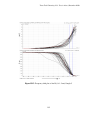
Figure 1.5: Engineering stress versus engineering strain curves for a 0.2 µm sample
for different strain rates
A sample engineering stress versus engineering strain curve is shown on Figure 1.5 for
0.2 µm foil for different strain rates. The yield stress (σy) is determined at a point on
the loading curve beyond which the linearity of the elastic regime is lost (correlation
coefficient at least 95%). The linear elastic part of the loading curve is determined
using best available linear fit as indicated by the corresponding correlation coefficient
(R2). The elastic modulus (E) is determined from the slope of the linear fit with an
error bar calculated from the corresponding R2 value as:
9
Texas Tech University, H. S. Tanvir Ahmed, December 2010
% of error = E (1-R2) × 100%
(1.5)
From Figure 1.5, it appears that the elastic modulus, measured at the onset of
yield point of the engineering stress versus engineering strain curve of the Ag foils
(for a particular pore size), is constant for the entire range of the strain rate. This
observation is taken into consideration that the average elastic modulus for a particular
pore size sample does not depend on the rate of loading and should remain constant.
Figure 1.6 shows the average elastic modulus as a function of porosity for different
pore size samples. Using linear fit, the porosity at which the elasticity would go to
zero (i.e., the elastic modulus at critical porosity Pc) is calculated to be 65.5% and the
elastic modulus for fully dense Ag (i.e. at porosity P=0) is estimated to be 25.07 GPa.
30
25
Elastic modulus (GPa)
2
E = -38.269(P) + 25.074, R = 0.9959
20
15
10
5
0
0
0.1
0.2
0.3
0.4
0.5
Porosity
Figure 1.6: Average elasticity plot for different porosity samples
10
0.6
Texas Tech University, H. S. Tanvir Ahmed, December 2010
Elastic constant of fully dense Ag in pure tension is reported to be c11=124.0
GPa [34]. Other elastic constants are reported as: c12=93.4 GPa, c’=½(c11-c12) =15.3
GPa and c44=46.1 GPa [34]. These values are in well agreement with the reported
values for silver at room temperature by Neighbours and Alers [35] and by Overton
and Gaffney [36], i.e., c11=123.99 GPa, c12=93.67 GPa, c’=15.16 GPa and c44=46.12
GPa. Similar values are obtained by Hiki and Granato [37], Chang and Himmel [38]
and Wolfenden and Harmouche [39]. The stiffness constants for cubic structure of Ag
are calculated as follows (c11=123.99 GPa, c12=93.67 GPa and c44=46.12 GPa):
s11 =
c11 + c12
= 0.023058 (GPa)-1
(c11 − c12 )(c11 + 2c12 )
(1.6)
s12 =
−c12
= −0.009923 (GPa)-1
(c11 − c12 )(c11 + 2c12 )
(1.7)
s44 =
1
= 0.02168 (GPa)-1
c44
(1.8)
With the stiffness constants, the directional (surface) elastic modulus E for the cubic
system is given as [40]:
1
1
= s11 − 2( s11 − s12 − s44 )(l 2 m 2 + m 2 n 2 + n 2l 2 )
E
2
(1.9)
where, l, m and n are the direction cosines. For (100), (110) and (111) directions, the
direction cosines are (1,0,0), (
1
1
1 1 1
,
,0) and (
,
,
) respectively. Thus, the
2
2
3 3 3
surface moduli E(100), E(110) and E(111) are calculated to be 43.37 GPa, 83.42 GPa
and 120.51 GPa respectively. The Ag samples used in this experiment do not have any
11
Texas Tech University, H. S. Tanvir Ahmed, December 2010
specific orientation of grains and are polycrystalline in nature. So, the elastic modulus
of these foils does not necessarily have any preferential direction and is obtained by
experiment. The multiple monotonic tensile tests conducted over a strain rate range of
10-4/sec to 10-1/sec yield an average Young’s modulus E of dense silver to be around
36 GPa. The shear modulus G and bulk modulus K are calculated here for reference,
using the following equations:
G=
1
= 15.16 GPa
2( s11 − s12 )
(1.10)
K=
EG
= 103.87 GPa
3(3G − E )
(1.11)
400
-1
ἐ=10 /sec
-3
-2
ἐ=10 /sec
ἐ=10 /sec
-4
ἐ=10 /sec
350
Engineering Stress σ (MPa)
300
250
200
150
100
50
0
0
0.005
0.01
0.015
0.02
0.025
0.03
0.035
0.04
Engineering Strain ε
Figure 1.7: Engineering stress-strain plot of fully dense silver at different strain rates
12
Texas Tech University, H. S. Tanvir Ahmed, December 2010
45
Elastic modulus E (GPa)
40
35
30
25
20
15
1.00E-05
1.00E-04
1.00E-03
1.00E-02
1.00E-01
1.00E+00
Strain rate
Figure 1.8: Elastic modulus of fully dense silver measured at different strain rates
The elastic modulus of fully dense silver from the plot of Figure 1.6 is
estimated towards a value in between the G and E value by the linear trend line, as
porosity goes to zero. For comparison, similar rate dependent tensile tests are done on
fully dense silver (99.95% pure) specimens and the measured elastic moduli are
plotted on Figure 1.7 and Figure 1.8. The average elastic modulus of dense silver is
calculated to be 36.35±1.54 GPa from these experiments. However, lack of surface
finish of the specimens may undermine the value by a bit. The author believes the
major discrepancy to be resulting from the surface irregularities and micro-cracks
present in the sample, as evidenced from the cross-section image on Figure 1.3. Some
level of stress-concentration factors are also introduced during the making of the
13
Texas Tech University, H. S. Tanvir Ahmed, December 2010
specimens using the die. These affect the yield strength and the elastic modulus of the
samples. Error in strain measurement, cross-section measurement and alloy impurity
plays a significant role in mechanical properties of the material. Also, for
polycrystalline samples, there is a possibility of mixed mode deformation (comprising
of shear, bending and tension) between the grains, which may lead to lower elastic
modulus.
The linear extrapolated value of elastic modulus of dense silver from Figure
1.6 and the actual value obtained through experiments are close (25.07 GPa as
opposed to 36.35 GPa), but not in good agreement with each other. There can be
several underlying reasons for this. In open cell foams, the initial deformation occurs
through bending [2], which may lower the elastic moduli of the porous samples as
well as the extrapolated value. The validity of the linearity of the elastic regime of the
stress-strain curve of porous samples is limited due to the early plastic deformations
[41], as random pores essentially work as micro-cracks in the sample. These reasons
suggest that a linear extrapolation may not be ideal for estimating elastic modulus at
varying porosity.
For estimation of the fully dense elastic modulus and critical elasticity, several
researchers proposed specific equations other than using a linear curve fit. Yeheskel,
et al. [42] used two different equations to predict the elastic modulus of fully dense
solids which are:
Es =
E
(1 − k1 P )
(1.12)
14
Texas Tech University, H. S. Tanvir Ahmed, December 2010
Es = Ee k2 P
(1.13)
where, Es is the elastic modulus of the fully dense solid, E is the elastic modulus of
porous material, P is the porosity and k1 and k2 are fitting coefficients. As discussed
earlier, the E value of fully dense silver is measured to be 36.35 GPa. Taking this
value as Es and taking k1 and k2 to be 1.25 and 3.45, respectively, equation (1.12) and
(1.13) are plotted on Figure 1.10. In these cases, the critical porosity Pc (porosity at
which the strength becomes zero) is derived from the prediction of the linear fit of the
strength plot and is approximated to be 80%. The assumption of zero strength at 80%
porosity originates from the strength plot and is discussed later in this section.
Gibson [2] proposed a relative approach for the estimation of the Young’s
modulus of the open-cell porous membranes:
ρ
E
=C
Es
ρs
2
(1.14)
where, E and ρ are the elastic modulus and density of the membrane, respectively. The
E
relative modulus is plotted as a function of the relative density
Es
ρ
ρs
in Figure
1.9 and the data are fitted with a power law. As a crosscheck to the reported value of
the coefficient C (which is a constant related to the cell geometry) to be 0.98 [43, 44]
and the exponent to be 2 [2], the values found here are 0.9946 and 2.6714,
respectively.
15
Texas Tech University, H. S. Tanvir Ahmed, December 2010
1.2
1
2.6714
E/Es = 0.9946(ρ/ρs)
2
, R = 0.9765
E/Es
0.8
0.6
0.4
0.2
0
0
0.2
0.4
0.6
0.8
1
1.2
(ρ
ρ/ρ
ρs)
Figure 1.9: Relative elastic modulus as a function of relative density
Li and Aubertin [45] proposed a general equation for the prediction of uniaxial strength based on actual porosity P and critical porosity Pc as follows:
σs
π P
x2 π P
+ σ s cos
× 1 −
2 Pc
2 Pc 2σ s
σ P = σ s 1 − sin x
1
(1.15)
where, σP is the strength at a particular porosity P, σs is the strength of the fully dense
solid (corresponding to P=0), x1 and x2 are material parameters and
are the
MacCauley brackets ( z = 0.5( z + z ) ). This equation can be used for both tension
and compression. Hence, the MacCauley brackets are used to take care of the sign of
16
Texas Tech University, H. S. Tanvir Ahmed, December 2010
the stress. Under tensile conditions, the author [45] reported a reduction of equation
(1.14) which is given by:
π P
2 Pc
σ P = σ s 1 − sin x
1
(1.16)
A similar approach is taken to generate functions for trendlines for the elastic
modulus, with one inflection point near the critical porosity and another inflection
point near the fully dense modulus value:
π P
b π P
E = 0.5 Es 1 − sin a
+ cos
2 Pc
2 Pc
(1.17)
π P
E = Es 1 − sin c
2 Pc
(1.18)
where E, Es, P and Ps hold same notions as described earlier. Approximating a, b and
c to be 0.25, 2.2 and 0.83, respectively, equation (1.17) and (1.18) are plotted in
Figure 1.10, along with other trendlines for prediction of elastic modulus.
The approximations of a, b and c are generated from the interest of making the
trendlines go through the experimental data set as closely as possible. Using different
critical porosity values (Pc) may result in a better fit. However, in this case, the
intention is to compare different equations with the same base parameters. As it can be
seen from Figure 1.6 and Figure 1.10, both equation (1.13) and equation (1.18) are
good approximations for elastic modulus at different measured porosity.
17
Texas Tech University, H. S. Tanvir Ahmed, December 2010
40
Porous Silver
Dense Silver
Equation (1.12)
Equation (1.13)
Equation (1.17)
Equation (1.18)
35
Elastic modulus (GPa)
30
25
20
15
10
5
0
0
0.1
0.2
0.3
0.4
0.5
0.6
0.7
0.8
0.9
Porosity
Figure 1.10: Trend lines for prediction of elastic modulus of Ag at different porosity
In addition to the role of porosity on elastic modulus, the dependency of
mechanical yield strength on structural features of the porous membranes is
investigated here. A Hall-Petch formulation [46, 47, 48, 49, 50, 51, 52] is indicative of
dislocation based plasticity and relates the dependency of strength to the square root of
structural size:
σ = σ0 +
kσ
(1.19)
hg
where, σ is the yield strength, σ0 is the intrinsic strength, kσ is the strengthening
coefficient and hg is the measure of dimensional size. Since, the grain size of the
porous sample sets does not vary beyond the statistical standard deviation, a Hall18
Texas Tech University, H. S. Tanvir Ahmed, December 2010
Petch evaluation of yield strength depending on structural dimensional feature (for
example grain size) is not possible. Even though a similar statistical trend exists with
the pore size of the samples, structural features like grain size or filament size does not
provide such a correlation. To estimate the yield strength at the fully dense condition,
the yield strength versus porosity plot of Figure 1.11 at every strain rate is
extrapolated to P=0 to provide an intercept value with a linear fit.
200
σ y = -180.95(P ) + 153.28, R2 = 0.9427, (ε ' =0.1000/sec)
σ y = -182.79(P ) + 145.74, R2 = 0.9247, (ε ' =0.0100/sec)
σ y = -155.91(P ) + 127.85, R2 = 0.9602, (ε ' =0.0010/sec)
σ y = -161.25(P ) + 129.01, R2 = 0.8986, (ε ' =0.0001/sec)
Yield strength σ y (MPa)
150
100
50
0
0
0.1
0.2
0.3
0.4
0.5
0.6
0.7
0.8
0.9
Porosity (P )
Figure 1.11: The yield stress versus porosity plot of different membranes at different
strain rates
The intercept values at P=0 range from 127 to 153 MPa as the strain rate
increases from 10-4 per second to 10-1 per second. The average tensile strength of
annealed silver wire is reported to be 125 MPa [53]. The strength values at each strain
19
Texas Tech University, H. S. Tanvir Ahmed, December 2010
rate at zero porosity may be representative of shortest structural dimension, i.e. the infilament grain size which is the average of the grain size values listed in Table 1.1 and
is calculated to be 2.47±0.19 µm. The grain size information of the annealed silver
wire is not available and hence, the strength of 125 MPa may not be an appropriate
value to do the comparison with. Moreover, the associated purity of silver plays a big
role on its strength [54]. For another comparison, the fully dense Ag samples are
tested in the same strain rate range, i.e., 10-4 to 10-1 per second and is plotted in Figure
1.11 at P=0, representing the fully dense state. In this case, the yield strength at fully
dense condition is higher compared to the extrapolated values. The fully dense
samples are assumed to be cold rolled during their production as 50 µm foils and
hence could have higher strength compared to annealed samples. Since the yield
strength of samples depends on the grain size, the information of that structural feature
on the fully dense samples is yet to be investigated which would enable their
characterization in a better way. Nevertheless, the overall trend of the increase of
strength estimation at P=0 seems reasonably satisfactory.
From Figure 1.11, a ‘zero’ intercept yield strength is estimated at an average
porosity of 81.8±1.8% which appears to be invariant with the change in strain rate.
The general trend of the yield strength appears to decrease in a linear fashion with
increasing porosity, though it seems that at higher porosity values, the strength may
decrease more rapidly. In accordance with equation (1.15), the effect of porosity on
strength of porous materials has been studied by Aubertin and Li [55] and has been
shown that the plastic deformation in porous materials occur in more than one way
(tension, shear, bending, etc.). The non-linear relationship of multi-axial inelastic
20
Texas Tech University, H. S. Tanvir Ahmed, December 2010
deformation leading to the strength of the porous material as a function of porosity is
proposed [45] as shown in equation (1.15). As stated earlier, this equation reduces to
equation (1.16) under uniaxial tensile condition. Figure 1.12 shows the trend lines
based on equation (1.15) and Figure 1.13 shows the trend lines based on equation
(1.16) as a function of porosity for different strain rates. In these figures, the
experimental value from fully dense silver is not plotted, as these values are not
appropriate for comparison, most likely, because of different grain size. In Figure
1.12, x1 and x2 are fit as 6 and 2 respectively, critical porosity Pc=80%. The critical
porosity and the intercept strength values at P=0 are determined using curve fitting
with the experimental data. In linear fit, the critical porosity value comes to be about
81% (Figure 1.11). Hence these two Pc values are in good agreement with each other.
However, the intercept values of yield strength come out to be lower than that
predicted by the linear fit. The experimental values of yield strength of fully dense
foils are not presented here and will be ignored in further plots, because there is an
apparent distinction of grain sizes between the fully dense and porous samples.
In Figure 1.13, on the other hand, the cosine term of equation (1.15) is
neglected. In fact, for pure tension, the terms in the MacCauley brackets of equation
(1.15) become zero and hence the cosine term disappears [45]. In the resulting
equation (equation (1.16)) x1 is assumed to be 4.5 with the critical porosity at 80% and
the trend lines are fitted to the existing experimental data. Even though the overall fit
for the experimental data seems to be very good, the prediction for intercept values at
P=0 are lower with these trend lines compared to those with linear fit (Figure 1.11) or
with equation (1.15) (Figure 1.12).
21
Texas Tech University, H. S. Tanvir Ahmed, December 2010
140
έ=0.1000/sec
έ=0.0100/sec
έ=0.0010/sec
έ=0.0001/sec
120
Yield strength σ y (MPa)
100
80
60
40
20
0
0
0.1
0.2
0.3
0.4
0.5
0.6
0.7
0.8
Porosity
Figure 1.12: Strength as a function of porosity (equation (1.15))
Strain rate sensitivity is the ability of the material to uniformly plastically
deform under load, without the localized concentration of stress and originates in the
formula given by Dorn:
σ = c(ε m )
(1.20)
where, σ is the stress, c is a constant, ε is the strain rate (i.e., ε/t) and m is the strain
rate sensitivity exponent. Thus, from the power law fit, the strain rate sensitivity is
obtained as the slope of the fit and is given by:
m = ∂ (ln σ ) / ∂ ln(ε )
(1.21)
22
Texas Tech University, H. S. Tanvir Ahmed, December 2010
The measured yield strength from the engineering stress versus engineering
strain curves of different porosity samples are plotted in Figure 1.14 as a function of
strain rate in a logarithmic scale. The overall strain rate dependent behavior of the
porous membranes having similar grain size (hg) is also plotted in this figure (i.e., the
intercept values of linear fit on Figure 1.11). And finally, the experimental data set of
the dense silver is plotted for comparison. The data points are fitted with power law
relationship from which the strain rate sensitivity is obtained for each sample set.
120
έ=0.1000/sec
έ=0.0100/sec
έ=0.0010/sec
έ=0.0001/sec
Yield strength σ y (MPa)
100
80
60
40
20
0
0
0.1
0.2
0.3
0.4
0.5
0.6
0.7
0.8
Porosity
Figure 1.13: Strength as a function of porosity (equation (1.16))
The analysis for variation of yield strength of the porous samples with strain
rate for the grain size case (hg) yields a strain rate exponent of 0.0281±0.00383 and
that for the fully dense samples yields 0.0215±0.00219. Even though these two rate
23
Texas Tech University, H. S. Tanvir Ahmed, December 2010
sensitivity exponent values are close to each other, the trend line for dense silver is
positioned above in Figure 1.14 compared to that of the hg line of the porous silver,
which means, the dense silver has higher strength compared to porous silver at a
particular strain rate. This means that the particular dense silver foils used in these
experiments have smaller grain size compared to the rest of the porous membranes.
This difference in the strength plot may originate from work hardening of the samples
as well, perhaps during their production as films. So, the rate sensitivity exponent (m)
may follow the grain size trend (higher m with decreasing hg) but the yield strength
may not.
215
195
Yield strength (MPa)
175
0.2 micron
0.45 micron
0.8 micron
3.0 micron
hg=2.47 micron
Fully dense Ag
y = 201.1x
0.0215
2
R = 0.8983
155
135
y = 162.92x
0.0281
2
R = 0.8636
115
95
y = 111.81x
0.0347
2
R = 0.9977
y = 97.635x
0.0249
2
R = 0.5161
75
55
y = 79.847x
0.0498
2
R = 0.9949
y = 57.012x
35
1.0E-05
1.0E-04
1.0E-03
1.0E-02
1.0E-01
0.0278
2
R = 0.6612
1.0E+00
Strain rate (1/sec)
Figure 1.14: The log-log plot of yield strength versus strain rate. The values are fit
with a power-law relationship to produce the strain rate exponent for each sample set.
24
Texas Tech University, H. S. Tanvir Ahmed, December 2010
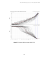
The variation of rate sensitivity exponent m generally depends on some
measure of structural feature size and generally increases with decreasing dimension
[19, 26, 56]. Most reports present the variation of ‘m’ with the change in grain size
(hg). The rate sensitivity of the porous membranes as a function of the grain size (hg) is
plotted on Figure 1.15. In addition, strain-rate exponents of nanocrystalline submicron
gold computed from the tensile tests [57] are plotted in this figure for comparative
reference of m to the dependency on grain size dimension of the porous membranes.
0.14
Au grain size
Ag grain size
0.12
Ag m(hg) eq
Strain-rate sensitivity m
0.1
0.08
0.06
0.04
0.02
0
0.1
1
10
100
Grain Size hg (µ
µm)
Figure 1.15: Strain rate sensitivity as a function of grain size
For nanocrystalline materials, an expression of rate sensitivity m with respect
to activation volume V for plastic deformation with a characteristic activation length
(or dislocation line length) L is found in the references [26, 58; 59]. Firstly, the critical
25
Texas Tech University, H. S. Tanvir Ahmed, December 2010
stress σ for bow-out of an edge dislocation from Frank-Read source in the slip planes
is expressed as [59]:
σ=
0.36Gb L
ln − 1.653
L b
(1.22a)
σ=
0.36Gb L 0.59508Gb
ln −
L
L
b
(1.22b)
where, G is the shear modulus of rigidity and b is the Burger’s vector. The constant
1.653 at the end of expression arose following the assumptions of edge dislocation and
a Poisson ratio of 0.33. Activation volume V equals Lb2 for dislocation based
deformation [26]. Relationship between activation volume and strain rate sensitivity is
originally proposed by Cahn and Nabarro [60] and is given by:
m=
3kT
V ⋅σ f
(1.23)
where, k is Boltzman constant (8.62×10⁻⁵ eV/K), T is temperature (K) and σ f is the
flow stress. The constant of
3 originates from assuming Von Mises criterion for
yielding and hence, converting the original expression of shear mode of deformation
to tensile mode of deformation. Using equation (1.22) and (1.23), the final relationship
between m and V is given as below:
0.5
1.5
3kT L L3
m=
ln
−
1.653
0.36G V V
The general relationship can be given as:
26
−1
(1.24)
Texas Tech University, H. S. Tanvir Ahmed, December 2010
1.5
3 0.5
L L
m = c1 ln − c2
V V
−1
(1.25)
where, c1 and c2 are constants depending on shear modulus G, Burger’s vector b and
temperature T. For experiments at the same room temperature, c1 and c2 will only
depend upon G and b. It is not possible to have dislocations extending beyond the
grain boundary limit. Hence, the upper limit of the length of dislocation line L should
depend on the grain size hg. Conceptually, L/hg approaches unity for very small hg and
asymptotically approaches very small values (or zero) for very large hg [59]. Based on
these physical boundary conditions, it can be reasonably assumed that for a single
grain larger than the theoretical limit of the grain size (where, the line length for a
single dislocation is basically the physical dimension of the grain):
L
~ hg − n
hg
(1.26a)
L = c ⋅ hg1− n
(1.26b)
where, c is a constant with the unit of (nm)n, n is an exponent that is less than unity.
The actual value of this power factor depends on the mechanism of deformation [26].
Assuming Hall-Petch relationship for large grain size, i.e., comparing the second term
of equation (1.22b) with that of equation (1.19), it is reasonable to assume:
L = c ⋅ hg
1
2
(1.27)
27
Texas Tech University, H. S. Tanvir Ahmed, December 2010
Hence, the value of the power factor n in equation (1.26b) is assumed to be ½. Thus,
assuming Hall-Petch, the functional relationship between grain size hg and strain rate
sensitivity m can be derived from equation (1.25) and (1.27):
1.5
L
m = c1 2
Lb
L3 0.5
ln 2 − c2
Lb
c2h
g
m = c1b −3 ln 2
b
0.5
− c2
m = c3 ln ( c4 ⋅ hg 0.5 ) − c5
−1
(1.28a)
−1
−1
(1.28b)
(1.28c)
where, c3, c4 and c5 are constants. Equation (1.28c) is used to curve fit (represented by
the dashed line on Figure 1.15) the hg value of m for silver taking c3, c4 and c5 to be
0.044, 15.3 and 1.65 respectively and assuming that for grain sizes above several
microns, typical m values are equal to 0.01–0.02. This corroborates with the findings
by Dao, et al. [19] for many fully-dense metals like nickel and copper. For porous
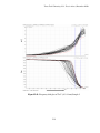
materials, it is proposed [1] that the filament size (i.e., the width of the filament) can
be considered as a measure of characteristic length instead. The reason proposed is
that the filament size is the medium for deformation and porosity is the free space.
With similar grain sizes, different membranes may possess different porosity with
different filament sizes and hence, should have different plasticity characteristics.
Whereas, the grain size based deformation will only be able to explain the overall
general trend, the filament size based deformation should allow for more detailed
characterization of the behavior. To evaluate this, the strain rate sensitivity data of the
28
Texas Tech University, H. S. Tanvir Ahmed, December 2010
membranes as a function of the filament size are plotted in Figure 1.16. Furthermore,
the final form of equation (1.28c) is used with filament size hf as the variable to
simulate a trend line for the m values:
m = c6 ln ( c7 ⋅ h f 0.5 ) − c8
−1
(1.29)
The constants c6, c7 and c8 are taken to be 0.03, 8.4 and 2.1, respectively. The trend
line is plotted as a dashed-dot line on Figure 1.16. It becomes very apparent from this
figure that the filament size based trend line better predicts the rate sensitivity
behavior of the membranes. Based on this trend line, it is also apparent that the rate
sensitivity value rises more rapidly as filament size gets smaller, as compared to the
grain size based trend line.
0.14
Ag filament size
0.12
Ag m(hg) eq
Ag m(hf) eq
Strain-rate sensitivity m
0.1
0.08
0.06
0.04
0.02
0
0.1
1
10
Filament Size hf (µ
µm)
Figure 1.16: Strain rate sensitivity as a function of filament size
29
100
Texas Tech University, H. S. Tanvir Ahmed, December 2010
As stated earlier, porosity may have an additional effect on deformation.
Porosity is a portrayal of the void space contained in the structure and also, is the
available space for the filaments or struts for deformation. Thus, it is proposed that
porosity is a measure of the activation volume. Porosity may couple with the filament
size and may consequence different rate sensitivity for membranes having same
filament size but different amount of available void space or porosity. Equation (1.25)
is adopted to use filament size as activation length and porosity as activation volume
and is given by:
1.5
3 0.5
hf hf
−
m = c9 ln
c
10
P
P
−1
(1.30)
0.14
Ag m(hg) eq
Ag m(hf) eq
0.12
Ag m(hf,p) eq
p=0.25
Strain-rate sensitivity m
0.1
P=.35
P=.5
0.08
0.06
0.04
0.02
0
0.1
1
10
Filament Size hf (µ
µm)
Figure 1.17: Porosity effect in strain rate sensitivity
30
100
Texas Tech University, H. S. Tanvir Ahmed, December 2010
Equation (1.30) is plotted as filled circle markers in Figure 1.17 for the specific cases
of the four different membranes used in this experiment, taking c9 and c10 to be
0.000367 and 2.21, respectively. Furthermore, trend lines for three different porosity
P=0.25, P=0.35 and P=0.5 (average porosity of 0.8 micron and 3.0 micron membranes
are quite close to 0.5) are also plotted in Figure 1.17 to show the general effect of
porosity on rate sensitivity. These trend lines are completely different from those
general trends plotted for grain size and filament size being the only variable. As seen
from this figure, the prediction of rate sensitivity governed by the solid trend lines
(using filament size and porosity as inputs) seems to be more accurate and
representative of the experimental data. It is also suggested that, higher rate sensitivity
exponent may be achievable for porous materials with larger filament sizes (larger
than ~5 µm where the local minima takes place), if the porosity is kept at a constant
value. At constant filament size, membranes with lower porosity will have higher rate
sensitivity.
1.3.2 Intermittent test of Ag foils
The continuous loading of the porous membranes in tension produces typical
engineering stress-strain curves, as shown in Figure 1.5. The linear elastic regime of
the loading curves is linearly fitted with highest correlation coefficient to obtain the
elastic modulus. It is seen from these tension tests that the elastic modulus of the
membranes does not change with the strain rate and remains fairly constant for each
porosity samples. However, for deformation of the membrane, it is postulated that the
porous membrane will first plastically deform as an open cell structure, and then
continue to deform wherein the open cell structure collapses through shear
31
Texas Tech University, H. S. Tanvir Ahmed, December 2010
deformation under tensile loading as the filaments (or struts) realign with the load
direction through a bending-shearing mode, primarily at the junctions between the
filaments [61]. Generally speaking, the junctions between filaments can be visualized
as ball joints with three degree of rotational freedom and the filaments align
themselves with the direction of the tension as loading starts and become parallel to
each other as the test specimen is loaded to its ultimate strength. Once the filaments
are aligned with the direction of the load, the structure will stiffen and the deformation
mechanism will change from shear towards uniaxial. For the deformation mode to
change, the elastic modulus measured from the tensile loading should also change as
the open filament structure condenses under tensile elongation. One way of assessing
this postulate is to do the intermittent tensile test wherein, the loading curve will be
interrupted after initial yielding, by complete unloading and reloading [57, 62]. The
reloading should go up to a load level beyond the yield load of the previous cycle.
Figure 1.18 shows a typical stress-strain curve for a 0.2 micron nominal pore size
membrane at 10-3/sec strain rate wherein the loading curve will be interrupted at
positions marked by horizontal dashed lines beyond the initial yield point and up to
the ultimate stress. It is suggested that an increase in the elastic modulus will progress
with the amount of plastic deformation until the ultimate strength level is reached.
Thereafter, localized necking will reduce the cross-section so that further deformation
will provide a decrease in the engineering stress and computed elastic modulus.
32
Texas Tech University, H. S. Tanvir Ahmed, December 2010
150
Engineering Stress (MPa)
125
100
75
50
25
0
0
0.01
0.02
0.03
0.04
0.05
Engineering Strain
Figure 1.18: Typical stress strain curve (20 point average of the original curve for 0.2
micron membrane at 10-3/sec strain rate) and positions of interruptions
As it is seen from Figure 1.18, for incremented tensile load tests beyond the
initial yield point, there are approximately five additional modulus measurements as
this porous sample is subjected to further plastic deformation at 10-3/ sec strain rate.
However, such number of additional measurements is not always possible. For slower
strain rates, there is enough time to manipulate the loading system. For increasing
strain rates, the number of measurements decreases as loading goes up very quickly
and interruption at an estimated load level (which has to be higher than the preceded
load) becomes difficult. For membranes with higher porosity, the interruption is
difficult even for lower strain rates, mostly because of their unpredictable strength
33
Texas Tech University, H. S. Tanvir Ahmed, December 2010
after the yielding and/or because of quick necking and fracturing. For this reason,
more than one test is done at each strain rate to achieve sufficient confidence level.
The incremental load curve for a 0.2 micron nominal pore size membrane tested at
10-3 per second strain rate is shown in Figure 1.19. With each successive interval of
time, the load is seen to increase.
22
20
17
N
Elastic modulus (GPa)
15
12
Load (N)
Ave Modulus from Tensile test
10
7
5
Elastic modulus (GPa)
load
2
0
0
50
100
150
200
250
300
350
400
450
-3
500
Time (sec)
Figure 1.19: Interrupted tensile test of 0.2 micron nominal pore size membrane at
10-3/sec strain rate to show the change in elastic modulus with progression of load
The modulus is measured (using corrected cross-sectional area) as the slope of the
linear portion to the loading curve for each increment. The elastic regime is identified
using a linear fit and a 20 point average trend line. The abscissa in Figure 1.19 is
34
Texas Tech University, H. S. Tanvir Ahmed, December 2010
shown in time (sec) to clearly demonstrate the succession of loading-unloading cycles
with increased load.
20
0.2 micron@1E-2
0.2 micron@1E-3
18
0.2 micron@1E-4
0.45 micron@1E-2
16
0.45 micron@1E-3
0.45 mciron@1E-4
Elastic modulus (GPa)
14
0.8 micron@1E-2
0.8 micron@1E-3
12
0.8 micron@1E-4
3 micron@1E-2
10
3 micron@1E-3
3 micron@1E-4
8
6
4
2
0
0
20
40
60
80
100
120
140
Strength (MPa)
Figure 1.20: The elastic modulus of porous silver membranes as measured through
incremented tensile loading are plotted as a function of the applied engineering stress
The variation in the elastic modulus with the measured engineering stress
(assuming the cross-sectional area being constant) is plotted in Figure 1.20. This
figure includes all of the modulus values from the onset of initial yielding through the
final yield point (i.e. the ultimate stress) as measured from each interrupted loading
interval. It can be seen from this figure that some modulus values decrease at a stress
level beyond the ultimate strength, indicating the loading regime wherein the
specimens undergo localized necking. Average modulus values are plotted for all the
35
Texas Tech University, H. S. Tanvir Ahmed, December 2010
tests conducted at each strain rate. It can be seen that the modulus values increase with
a decrease in porosity. Also, the modulus is found to increase with increasing plastic
deformation up to a certain limit wherein the stress level starts to drop because of
localized necking. The maximum modulus value is found in Figure 1.20 in the upper
plateau regions for each level of membrane porosity, irrespective of the associated
strain rates.
In a similar fashion, intermittent tests have been conducted on dense silver
specimens over 10-4, 10-3 and 10-2 per second strain rates. Figure 1.21 shows an
example of the resulting elastic modulus after each successive plastic deformation that
the sample goes through. Like the porous samples, the dense silver specimens also
show an increase in modulus at higher amount of plastic deformation. This increment
in modulus, too, plateaus out after certain amount of work hardening. Figure 1.22
plots all the data on elastic modulus of dense silver as a function of the applied
engineering stress over all the strain rates. The average of the maximum modulus
values (i.e. the plateau region) is shown with a horizontal line. These maximum elastic
modulus values (independent of strain rate) determined from the incremented tensile
tests are plotted as a linear function of membrane porosity in Figure 1.23.
36
Texas Tech University, H. S. Tanvir Ahmed, December 2010
100
45
load
90
N
Elastic modulus
40
80
70
30
Load (N)
60
25
50
20
40
15
30
Elastic Modulus (GPa)
35
10
20
5
10
0
0
200
400
600
800
1000
1200
0
1400
Time (sec)
Figure 1.21: Change in elastic modulus of dense silver with progression of load at a
strain rate of 10-3 per second
37
Texas Tech University, H. S. Tanvir Ahmed, December 2010
70
60
Elastic Modulus (GPa)
50
40
30
1.00E-02/sec
1.00E-03/sec
1.00E-04/sec
20
10
0
0
50
100
150
200
250
300
350
400
Strength (MPa)
Figure 1.22: Elastic modulus from interrupted test of dense silver as a function of
applied engineering stress over different strain rates
38
Texas Tech University, H. S. Tanvir Ahmed, December 2010
25
Continuous tensile test
Maximum value from interrupted test
2
y = -35.365x + 27.926, R = 0.9953
Elastic modulus (GPa)
20
15
10
2
y = -38.269x + 25.074, R = 0.9959
5
0
0
0.1
0.2
0.3
0.4
0.5
0.6
Porosity
Figure 1.23: Variation of elastic modulus with porosity for silver membranes as
measured using tensile test (initial onset of yielding) and interrupted test (at ultimate
strength)
From Figure 1.23, it is clearly evident that the porous membranes
progressively stiffen when subjected to increasing plastic deformation. The intercept
value found using a linear fit for the stiffened modulus suggests a small increment
from 25.07 GPa at the initial yield condition to 27.93 GPa at the maximum stiffened
condition (i.e. at ultimate stress). This suggests that higher porosity membranes stiffen
more under progressive loading compared to lower porosity membranes. Both
monotonic loading and interrupted loading predicts similar elastic modulus values at
fully dense condition. The linear extrapolation of the curve for maximum modulus
39
Texas Tech University, H. S. Tanvir Ahmed, December 2010
value in Figure 1.23 also suggests the critical porosity Pc (porosity at which strength
goes to zero) to be 0.79, which is in very well agreement with modeling data found
from tensile testing.
1.3.3 Tensile test of electrodeposited nanocrystalline Ni
The tensile test specimens on nanocrystalline Nickel are obtained as pulsed
electrodeposited thin films [63] on stainless steel surface. Copper is used as a buffer
layer on the stainless steel to provide the ease of removing the deposited nickel. Free
standing test pieces are laser cut to have a nominal width of about 1.4mm, while the
thickness of the specimens is determined by the as-deposited condition, being
nominally about 50 microns. The test specimens are mounted on the tensile tester
using heavy-duty serrated grips (Figure 1.24).
Figure 1.24: Serrated grips for mounting the nanocrystalline Ni foils
40
Texas Tech University, H. S. Tanvir Ahmed, December 2010
Rate sensitive tensile testing is done on the samples using the same technique
as described in section 1.3.1 Tensile test of Ag foils. The tests are carried out at strain
rates of 10-5 to 10-1. For each strain rate, at least two or three samples are tested to
failure and the data is recorded as a function of time. Optical microscopy of the crosssections of the samples after failure is done at various magnifications to provide more
accurate measurements of the thickness and width and also, to provide some
identification of ductile or brittle failure. A typical optical image of the thickness of
such a foil at about 600X magnification is shown on Figure 1.25. The yield strength is
measured from the engineering stress versus engineering strain curve at a point where
the linearity of loading starts to deviate. The linear loading regime is defined using a
20-point moving average and a linear fit. The highest correlation coefficient of the
linear fit provides the limits of the linear part while the 20-point average shows an
overall behavior. Figure 1.26 shows a comparative plot of the engineering stress
versus engineering strain curves at different strain rates measured at room
temperature. The measured yield strengths of the samples are plotted on Figure 1.27 as
a function of the applied strain rate on a logarithmic scale. The exponent of the power
law fit of the data points provides the strain rate sensitivity of the nickel specimens.
A linear relationship is fitted on plot of ln(strain rate) versus yield stress (in
units of MPa) to reveal the activation volume (Figure 1.28). The activation volume V
is given by [60]:
V = k BT
∂ ln ε
∂σ
(1.31a)
41
Texas Tech University, H. S. Tanvir Ahmed, December 2010
∂ ln ε
V
=
k BT
∂σ
(1.31b)
where, kB is the Boltzman constant (1.381×10⁻²³ J/K) and T is the temperature. The
slope of ln(strain rate) versus yield stress would give a value equal to
V
. At room
k BT
temperature (T=300K) the value of kBT equals to 4.142×10⁻²¹ J. Thus the activation
volume in nm3 is given by 4.142 times the slope of the linear fit of the above
mentioned plot, if yield stress is plotted in the units of MPa. Higher activation volume
means larger grain size and vice versa. The activation volume for this case becomes
0.0733nm3 which implies that the grain size of the nanocrystalline nickel is about 10
nm [26], assuming Burger’s vector for perfect dislocation. The atomic radius of nickel
is 124pm [64] and hence, the Burger’s vectors are given by [65]:
bperfect=
a
0.124 × 2
=
=0.175nm
2
2
(1.32 a)
bpartial=
1
bperfect=0.1012nm
3
(1.32b)
1
bmixture= (bperfect+bpartial)= 0.1381nm
2
(1.32c)
Thus, assuming perfect, partial and mixture type of dislocations, the activation volume
becomes 13.677b3, 70.72b3 and 27.83b3 respectively.
Figure 1.29 shows the strain rate sensitivity of nanocrystalline copper [19] and
nanocrystalline nickel [26] as a function of grain size. A general trend of increasing
42
Texas Tech University, H. S. Tanvir Ahmed, December 2010
rate sensitivity is observed with a decrease in grain size. This behavior is predicted by
using the formulation proposed by Gu, et al. [26] in the following form:
m = c1[ln(c2 d ) − c3 ]−1
(1.33)
where, c1, c2 and c3 are constants depending on the shear modulus of rigidity (G) and
burger’s vector (b). This equation is based on the assumption of valid Hall-Petch
strengthening mechanism. A more detailed study on this derivation is documented in
the earlier section (1.3.1 Tensile test of Ag foils). The behavior of strain rate
sensitivity as a function of grain size is predicted using equation (1.33) and is plotted
on Figure 1.29. Here, c1, c2 and c3 are taken to be 0.018, 3.0 and 1.65 respectively
[66]. The value of strain rate sensitivity of the current study is also plotted in the same
figure and is in well accordance with both the previous experimental data found in
literature [26] and prediction by the model equation (1.33). The strain rate sensitivity
of these nanocrystalline nickel samples is found to be higher than the conventional
coarse-grained samples.
43
Texas Tech University, H. S. Tanvir Ahmed, December 2010
20 µm
Figure 1.25: A typical thickness of the nanocrystalline nickel as viewed under the
optical microscope at 600X magnification.
1400
1200
7.79E-02/sec
9.20E-03/sec
Engineering Stress (MPa)
8.28E-04/sec
1000
3.37E-05/sec
800
8.10E-05/sec
600
400
200
0
0
0.005
0.01
0.015
0.02
0.025
0.03
0.035
0.04
0.045
0.05
Engineering Strain
Figure 1.26: Engineering Stress-strain curves of NC nickel at different strain rates
44
Texas Tech University, H. S. Tanvir Ahmed, December 2010
Yield stress (MPa)
10000
y = 1116.8x
0.0561
2
, R = 0.7466
1000
100
1.00E-05
1.00E-04
1.00E-03
1.00E-02
1.00E-01
1.00E+00
Strain rate
Figure 1.27: Power law fit of the stress versus strain rate to provide the strain rate
sensitivity of nanocrystalline nickel
45
Texas Tech University, H. S. Tanvir Ahmed, December 2010
0
-2
2
y = 0.0177x - 20.73, R = 0.7708
ln(Strain rate)
-4
-6
-8
-10
-12
-14
300
400
500
600
700
800
900
1000
1100
1200
1300
Yield stress (MPa)
Figure 1.28: Activation volume is calculated from the slope of linear fit of ln(strain
rate) versus yield stress
46
Texas Tech University, H. S. Tanvir Ahmed, December 2010
0.08
Ni and its alloys from Gu et al
Cu and its alloys from Dao et al
0.07
Strain-rate sensitivity exponent m
This study
Predicted by equation
0.06
0.05
0.04
0.03
0.02
0.01
0
1.E+00
1.E+01
1.E+02
1.E+03
1.E+04
1.E+05
1.E+06
1.E+07
Grain size d (nm)
Figure 1.29: Strain rate sensitivity of Cu [19] and Ni [26] as a function of grain size
1.3.4 Tensile test of nanocrystalline Au-Cu foils
The nanocrystalline Au-Cu alloys have a composition of Au(100-x)-Cu(x) where
x< 20 weight percent and are about 20 µm in thickness. The free-standing foils are
synthesized [27, 28, 29] using electrodeposition through pulsed current. The laser-cut
foils are tested to failure in tension using the TestResources tensile testing machine
and are mounted using wire grippers. Rate sensitivity experiments are performed by
moving the linear actuator over a constant distance while varying the test time. Figure
1.30 shows a representing load-time plot for a Au-Cu sample. SEM images are taken
of the failed cross-section to determine the width. Figure 1.31 shows such an image
from which the width of the corresponding sample was determined. Highest load
value from the load-time plot is taken to obtain the ultimate strength of the sample.
47
Texas Tech University, H. S. Tanvir Ahmed, December 2010
4
3.5
3
Load (N)
2.5
2
1.5
1
0.5
0
13
14
15
16
17
18
19
20
Time (sec)
Figure 1.30: Load-time plot for a Au-Cu sample
Figure 1.31: SEM image is used on failed cross-section of a Au-Cu sample for
measuring the width.
48
Texas Tech University, H. S. Tanvir Ahmed, December 2010
500
450
Tensile strength (MPa)
400
y = 810.14x
0.1393
2
, R = 0.8514
350
300
250
200
150
100
0.0001
0.0010
0.0100
Strain rate (1/sec)
Figure 1.32: Strain rate sensitivity plot for the Au-Cu samples
Figure 1.32 shows the log-log plot of tensile strength versus strain rate. The
data points are fitted with a power law relationship to determine the strain rate
sensitivity exponent. The grain size of the samples used in this experiment is
calculated [27, 28, 29] to be 10.33 nm. The strain rate sensitivity exponent value (i.e.,
m= 0.1393) from this experiment is in a very well agreement with the micro-scratch
results obtained by Nyakiti and Jankowski [66] and is shown in Figure 1.33 as a
function of log-scale grain size (dg). Equation (1.33) has been used to predict the
behavior of these nanocrystalline Au-Cu samples. The constants c1, c2 and c3 are taken
to be 0.080, 3.0 and 1.65 respectively [66].
49
Texas Tech University, H. S. Tanvir Ahmed, December 2010
0.25
Results from Nyakiti and Jankowski
This experiment
Strain rate sensitivity m
0.2
Predicted by equation
0.15
0.1
0.05
0
1
10
100
1000
Grain size d g (nm)
Figure 1.33: Strain rate sensitivity as a function of grain size for nanocrystalline
Au-Cu samples.
1.4 Summary
1. Tensile testing of porous silver membranes and fully dense foils are done at
various strain rates. The measured elastic modulus for the porous membranes appear
to be indicative of the G modulus and follows a trend line as the porosity goes from
~80% to fully dense condition. The change of yield strength with porosity has been
modeled with the theory of Li and Aubertin [45] and is found to have good correlation
with the experimental data. A 2.47 µm average grain size of the membranes is
measured from SEM images of the porous membranes and is somewhat invariant with
porosity. Strain rate sensitivity found from the rate dependent tensile testing has been
plotted as a function of the grain size and is in well accordance with the analytical
50
Texas Tech University, H. S. Tanvir Ahmed, December 2010
model provided by Gu, et al. [26]. Alternately, it is proposed [1] that strain rate
sensitivity exponent can be modeled if the filament size and porosity are substituted in
the analytical equations. Models for these expressions in equations (1.29) and (1.30)
are plotted in Figure 1.16 and Figure 1.17 against the experimental data and are found
to be in good agreement. The implication is that strain rate sensitivity exponent will
increase as the filament size decreases, and will increase more rapidly as porosity
increases.
2. Interrupted tensile tests are done on porous silver membranes at different
strain rates to show the stiffening behavior of porous materials under tensile loading. It
is observed that the membranes show an elastic modulus close to the G value.
However, as deformation progresses, an upper plateau in the elastic modulus is
approached that is different than modulus found in monotonic loading conditions. This
upper plateau in the modulus measurement is more indicative of a value close to that
measured for fully dense silver foils. It is anticipated that elastic modulus can increase
for materials that strain harden by as much as 10-15%, i.e., Figure 1.22 data. Thus, it
is postulated that the filaments (or struts) are linked with each other with “ball joints”
that would, in essence, realign to each other in the direction of applied load. This
realignment of the load bearing filaments gives the membrane more elasticity provided
that necking is not yet formed.
3. Rate dependent tensile testing has been conducted on nanocrystalline
electro-deposited nickel to provide the strain rate sensitivity. The as-deposited
condition provides the necessary shape for the test specimens. The thickness and
width of the samples are better estimated using optical microscopy. The activation
51
Texas Tech University, H. S. Tanvir Ahmed, December 2010
volume is found to be about 0.07 nm3 which is suggestive of a grain size below 10 nm.
The rate sensitivity is plotted as function of the grain size and is found to follow the
similar trend from literature data for Hall-Petch strengthening mechanism. The
experimental data is modeled based on an analytical model of bow-out of an edge
dislocation [26, 59] and has good correlation with the plotted trend line.
4. Nanocrystalline Au-Cu samples are tested in tension at different strain rates.
Strain rate sensitivity exponent of the samples has been obtained through a log-log
plot of the strength versus strain rate. The 10.33 nm grain size samples show a strain
rate exponent of 0.1393. This value is very close to projected value by the trend line
obtained by Nyakiti and Jankowski [66] through micro-scratch testing of Au-Cu
samples with different weight percent of Cu.
52
Texas Tech University, H. S. Tanvir Ahmed, December 2010
CHAPTER 2
MICRO-SCRATCH TESTING OF POROUS MEMBRANES
2.1 Introduction
Mechanical behavior of materials on a wide range of strain rates has been of
interest to many researchers [e.g.: 19, 20, 57, 62, 67, 68, 69, 70]. Most materials are
known to have different strength at different rate of loading, hence, exhibits at least
some level of strain rate sensitivity. Many testing methods, for example, tension,
compression, torsion, etc. can be applied to reveal the rate sensitive nature of
materials. Among those, tensile [1, 27, 31, 57, 62, 71] and compression tests [11, 12,
13] are probably the most common method of testing specimens for about 10-4 to 10-1
per second strain rates [1, 20, 27, 69]. At the slower end of strain rate experiments
with tensile tester has a difficulty of not being able to deform the sample in a highly
continuous (or monotonic) fashion. In most cases, the linear actuator of the instrument
for tensile deformation moves in a discrete manner in slower rates, which become
evident from the plot of load versus time recording. Clusters of data points can be seen
in the load-time curve as the actuator moves and tries to keep up with the input signal
at such slower speeds. At faster rates, the major problem lies with the speed of data
acquisition. In spite of these practical issues associated with the hardware of the
experimental setup, tensile test provides highly accurate estimates of the stress-strain
plots of the materials.
Faster rate tests, for example, 100 to 10+4 per second strain rates are mostly
reported to be conducted by Split Hopkinson Pressure Bar (SPHB) technique [72, 73,
74, 75, 76]. In this setup, a gas driven projectile hits an incident bar while the
53
Texas Tech University, H. S. Tanvir Ahmed, December 2010
specimen is situated between the incident bar and a transmitter bar. Both these
incident and transmitter bars have significantly large dimensions compared to the
specimen size and are equipped with strain gauges. Data are recorded from these strain
gauges from these bars as the specimen is compressed in the in-between position.
Despite its popularity, there are some reports that indicate that SHPB results may
sometimes be misleading [75, 76]. The major postulations behind SHPB experiments
rises from assuming uniform deformation of the sample (i.e. stress equilibrium) and no
frictional response of the system, which, sometimes are not the actual case.
As an alternative, scratch hardness measurements, originally introduced by
Mohs in 1824 [77], have evolved as a method for measuring mechanical properties of
bulk materials and thin films. Rate sensitive scratch tests can be done to reveal the
strain rate sensitivity of a material. Inherent rise time for scratch velocity prohibits the
sample from being shock loaded. Also, the scratch test method is not as sensitive to
the internal flaws and defects present the material as it is for tensile experiments at
high rates. In tensile tests, the internal defects present in the test material often lead to
premature failure through the stress concentration effect. Significant variation [31, 60
71] can result in the measurement of strength from such high rate tensile tests. As
such, scratch testing can be utilized as a better option for testing materials at high
strain rates. The aim of this research is to conduct micro-scratch experiments on
porous silver foils to high strain rates and compare the results with tensile tests, to
generate a longer range strain rate sensitivity plot for the porous silver membranes.
54
Texas Tech University, H. S. Tanvir Ahmed, December 2010
2.2 Background
Several researchers documented a change in the sensitivity exponent for
various material systems as they compared uniaxial compression test with Split
Hopkinson Pressure Bar (SHPB) test for a wide range of strain rates. Freund and
Hutchinson [78]studied the problem of crack growth in plastics in high strain rate and
reported the existence of a transition shear stress at a transition plastic strain. Below
that transition stress, the dislocation motion is controlled by lattice resistance or
discrete obstacles and above that transition stress the regime is controlled by phonon
drag. Armstrong and Zerilli [79] reported similar transitioning behavior towards high
rate sensitivity for copper and α-iron. Follansbee [80] speculated that limited
dislocation mobility by phonon drag could lead to higher rate sensitivity.
A general description of the mechanical response associated with rate
sensitivity is given by Harding [72]. He summarized the strain-rate response of
materials into three major categories, with corresponding rate controlling mechanisms.
These three regions are shown in the following schematic (Figure 2.1) labeled as I, II
and III.
55
Texas Tech University, H. S. Tanvir Ahmed, December 2010
III
Yield Stress
I
II
Log (strain rate)
Figure 2.1: Schematic of different regions of rate sensitivity
The first segment, denoted as I, is referred to the region where low strain rates
and high temperatures are active and has almost a constant, rate independent flow
stress. The major underlying rate controlling mechanism in this region in stated to be
athermal flow, where presence of precipitates puts forward long-range friction stress.
Thermal vibrations in the lattice are insufficient in providing energy to overcome this
long-range barrier. Even though crystal structure of the material has some influences
on this athermal friction stress, the major positive contributions come from the
presence of alloy content in the material. Materials with higher alloy content will show
lower strain rate sensitivity [20, 72].
The second segment (II) is the region where higher strain rates are active at
lower temperatures [72] and a linear dependence of flow stress on the logarithmic
strain rate in observed. The transition from region I to region II is reported to be
around 10-1 strain rate for annealed mild steel at room temperature [72]. At this section
of the rate sensitivity, short range barriers such as dislocations and their interactions
become relatively more important compared to the long range barriers (i.e., alloy
56
Texas Tech University, H. S. Tanvir Ahmed, December 2010
content). The flow stress is thermally activated which means the lattice vibrations can
assist by supplying enough energy to overcome these barriers and flow stress becomes
dependent on temperature and strain rate.
At higher rates of strain, a significant increase in the rate sensitivity exponent
is observable, as shown in segment III (and as will be seen in the micro-scratch
experiments of the porous foils). Harding [72] reported this transition from segment II
to segment III at about 5×10+3 strain rate for annealed mild steel at room temperature.
Freund and Hutchinson [78] reported a similar transitioning strain rate (between 10+3
and 10+4 strain rate), however did not show the intermediate zone (region II) as a
separate section. Armstrong and Walley [74] collected a numerous results of research
conducted in this area in the review paper and stated that additional deformation
features such as deformation twinning, adiabatic shear banding and dislocation or twin
generations play very important roles in very high strain rate regime for shock loading.
They also reported that behavior of shock loading (as obtained from SHPB) and
shockless loading (with a continuous increase in load in a very small rise time) may
differ significantly and may be more governed by drag resisting velocities of
dislocations for shockless loading. This phenomenon is widely known as “phonon
drag”, whereas the original dislocation density is required to move at the upper
limiting speed, i.e. the speed of sound and rate exponent increases most likely because
of the “saturation of the mobile dislocations average velocity” [20].
Dioh, et al. [75, 76] studied the high strain rate properties of materials using
SHPB and demonstrated that in some case, the higher rate sensitivity above certain
strain rates is the outcome of generalization of the impact problem by assuming
57
Texas Tech University, H. S. Tanvir Ahmed, December 2010
equality of stress all over the deforming specimen. In reality, he showed that the stress
wave form generated by high impact velocity of the pressure bar induces stress and
strain gradients and thus, is different from uniform stress assumption that neglects the
dynamic effect.
Today, many researchers can now use scratch technique as a comparable
method for investigating mechanical properties of materials. Nyakiti and Jankowski
[66] studied rate sensitivity behavior of gold-copper alloys using micro-scratch
experiments. The range of micro-scratch strain rates was comparable with the limits of
tensile testing and thus, reported values of sensitivity exponents were consistent with
values as obtained by tensile tests.
2.3 Experimental methods and analysis
2.3.1 Micro-scratch experiment of porous silver foils
Membranes of varying nominal pore sizes (0.2, 0.45, 0.8 and 3.0 micron) are
procured from General Electric OsmonicsTM. The porosity of the membranes is
characterized using the same procedure as stated in Chapter 1. The estimation of grain
size is obtained with lineal intercept method (also explained in Chapter 1) on the plan
view images of the samples using a Hitachi S-4300 SE/N SEM. The samples are cut in
rectangular sizeable dimensions using an X-acto knife and are mounted on plan view
on a steel stub using epoxy glue on all four corners of the samples.
The micro-scratch experiments are conducted using a Universal Micro
TribometerTM (UMT), mounted on a mechanical vibration isolation table. A
spheroconical diamond Rockwell tip of 12.5 µm radius having 60-deg angle is used to
produce the scratches on the mounted samples. Figure 2.2 shows a typical set up for
58
Texas Tech University, H. S. Tanvir Ahmed, December 2010
conducting the micro-scratch test. A nominal load of 10 gm (98 mN) normal to the
sample surface is used to make the constant load scratches. During a scratch test, the
Y-stage of the UMT that contains the sample on it moves in the direction of the
scratch and the tip remains constant at its position, applying the load on the surface. A
force feedback system that records the applied force as a function of time is used to
measure the actual force and scratch velocity. To induce different velocities of
scratches, associated time is varied while the lengths of scratches remain same. Seven
different scratch velocities i.e. 0.3 mm/sec, 0.5 mm/sec, 1 mm/sec, 2 mm/sec, 3
mm/sec, 5 mm/sec and 10 mm/sec are used to produce all the scratches on the foils. At
least three scratches are produced at every scratch speed to obtain a good statistical
average. Figure 2.3 shows an optical microscope image of a sample containing all the
scratches at different velocities.
Figure 2.2: Micro scratch test rig
59
Texas Tech University, H. S. Tanvir Ahmed, December 2010
3 mm
Figure 2.3: Scratches at different velocities on a single membrane mounted on plan
view
Figure 2.4: A sample scan on one of the scratches using the profiler using a 0.7 µm
tip
60
Texas Tech University, H. S. Tanvir Ahmed, December 2010
The width of the micro-scratch profiles are scanned using a Veeco Dektak 150
surface profiler mounted on an air suspended table. The scan of the scratch width is
done using a spheroconical tip of radius 0.7 µm that has a 45 deg angle of inclination,
with a stylus tracking force of 8 mg (78.4 µN). Figure 2.4 shows a typical output from
the profiler which shows the scan of the width of a scratch and also shows the
background surface profile.
Since the material is porous, scan on an apparently ‘flat’ surface provides lots
of ups and downs. Thus, defining a horizontal background from which the scratch
width would be measured becomes difficult. Defining the marker positions to evaluate
the width is a challenge for the porous materials because of the associated high
‘surface roughness’. For measuring the width using the contact profilometer, the tilt of
the scan is adjusted first using wide left and right markers, to sample a considerable
segment of the background (as shown in Figure 2.4 using red and green marker
colors). Then, a horizontal line is drawn at the average step height of the membrane,
accompanied by two other horizontal lines which define at least 90% confidence level
of covering the roughness. Figure 2.5 illustrates the methodology. The width of the
scratch is measured at these three horizontal lines and an average of those widths is
taken to be representative of the particular scratch, i.e.
w=
w1 + w2 + w3
3
(2.1)
The scratch hardness (Hs) is computed by dividing the scratch load by the
projection of half of the area of the tip leading in the direction of the scratch. The
empirical expression is given by:
61
Texas Tech University, H. S. Tanvir Ahmed, December 2010
Hs = c
F
w2
(2.2)
where, Hs is the hardness, F is the scratch load and w is the associated width of the
scratch. The constant c is a geometric function related to the indenter tip shape.
Assuming that the scratch does not go beyond the initial hemispherical region of the
tip, c equals 8/π for the projection of the leading half area of the indenter. The
deformation path of the scratch is represented by the measured scratch width (w). And
usually, the depth of scratch is much less compared to the width of the scratch. Even
though the depth and width of the scratch are geometrically related to each other for a
well-defined tip, the depth of the scratch involves some level of elastic rebound of the
material. Scratch test involves primarily a shear type of deformation because the
material is sheared along the direction of the scratch. During this shear type of
deformation, the scratch width remains unchanged. Hence, the width of the scratch
offers a better measurement of the actual volume of the material that undergoes the
deformation. For this reason, the width of the scratch is used to determine the scratch
hardness in equation (2.2). The strain rate ( ε ) for micro-scratch experiments are
empirically derived [66] to be:
ε =
v
w
(2.3)
where, v is the velocity of the stylus producing the scratch and w is the resultant
scratch width. Strain rate sensitivity of strength (σ) for a material is given by famous
Dorn equation:
σ = cε m
(2.4)
62
Texas Tech University, H. S. Tanvir Ahmed, December 2010
where, m is the strain rate sensitivity exponent and c is a constant. Thus m is derived
from this equation by taking logarithm on both sides of equation (2.4) as:
m=
δ ln σ
δ ln ε
(2.5)
2
Elevation (µm)
1
0
W1
-1
W2
W3
-2
-3
-4
-5
-6
-7
20
40
60
80
100
120
140
Distance x (µ
µm)
Figure 2.5: Illustrating the measurement of the scratch width for porous materials
63
Texas Tech University, H. S. Tanvir Ahmed, December 2010
2
1
0
Height (µm)
-1
-2
-3
-4
10 mm/sec
-5
3 mm/sec
5 mm/sec
-6
0.3 mm/sec
-7
1 mm/sec
0.5 mm/sec
2 mm/sec
-8
0
20
40
60
80
100
120
Distance (µ
µm)
Figure 2.6: A comparative study of the width of scratches at different velocities on
0.45 micron foil
A plot of ln ε versus ln σ will yield a linear curve with a slope (m) equal to the strain
rate sensitivity. For the scratch test data, the hardness (Hs) is plotted rather than the
strength ( σ ), since hardness and strength are related according to σ ~ cH s , where c is
a constant having a typical value of 1/3 [81, 82].
The rate sensitivity plots of 0.2, 0.45, 0.8 and 3.0 micron pore size membranes
are shown in Figures 2.7-2.10, respectively. For reference, the yield strengths obtained
from the tensile tests as a function of strain rate are plotted as well. Material
deformation under scratch is mostly of shear type and hence, to compare the scratch
hardness with the tensile hardness (1/3 times the tensile strength), the scratch hardness
64
Texas Tech University, H. S. Tanvir Ahmed, December 2010
values are multiplied by √3. These hardness values (which are uniaxial in essence) are
plotted in the aforementioned figures. Figure 2.11 shows the rate sensitivity plot for
fully dense silver. From these figures, it can be seen that the slope of the data points
from different regions lie at different elevations. These discontinuities originate from
assuming a constant c value of 1/3 in strength-hardness relationship. These
discontinuities are more evident in higher porosity membranes (i.e. the slope of data
points from region II moves higher in elevation). At different level of indentations,
different tip geometry is active and hence, it is necessary to consider different
corresponding c values. However, for calculating strain rate sensitivity, only the slope
of the power law fit is important and the elevation of the plot (corresponding to
different c values) can be neglected without any significant error. From these figures,
it is also evident that for some specimens there may be little or no transitional zone
between low (region I) and intermediate (region II) strain rate sensitivity. These
phenomena can be observed for high porosity membranes (0.8 and 3.0 micron nominal
pore size) as well as for fully dense foil. To investigate any possible difference, similar
rate dependent micro-scratches are done on the cross-section of the dense samples.
The samples were prepared using epoxy mount in cross-section and involved grinding
and polishing at different smoothness levels to remove surface roughness and other
possible artifacts from the vacuum casting process. The data from scratch on plan
view and on cross-section overlaps, as it can be seen from Figure 2.11. It is also found
that at intermediate regime (region II) the rate sensitivity exponents of all porosity
membranes are somewhat comparable. Similar trend lines were reported by Harding
[72] in a study on commercial-purity aluminum (i.e. the higher strain rate exponents
65
Texas Tech University, H. S. Tanvir Ahmed, December 2010
are alike). Table 2.1 lists the strain rate sensitivity exponents obtained for different
regimes of all the specimens.
10000
Tensile Hardness (region I)
Micro-Scratch Hardness (transition)
Micro-Scratch Hardness (region II)
y = 1003.8x0.1316, R2 = 0.8804
Hardness (MPa)
y = 1488.4x0.0586, R2 = 0.8357
1000
y = 335.54x
100
1.0E-05
1.0E-04
1.0E-03
0.0318
2
, R = 0.9971
1.0E-02
1.0E-01
1.0E+00
1.0E+01
1.0E+02
1.0E+03
Strain rate (1/sec)
Figure 2.7: Rate sensitivity plot of 0.2 micron pore size membrane
66
1.0E+04
Texas Tech University, H. S. Tanvir Ahmed, December 2010
10000
Tensile Hardness (region I)
Micro-Scratch Hardness (transition)
Micro-Scratch Hardness (region II)
Hardness (MPa)
y = 810.2x
y = 1057.2x
0.0927
0.1319
2
, R = 0.7882
2
, R = 0.9694
1000
y = 299.43x
100
1.0E-05
1.0E-04
1.0E-03
0.0249
2
, R = 0.5161
1.0E-02
1.0E-01
1.0E+00
1.0E+01
1.0E+02
1.0E+03
Strain rate (1/sec)
Figure 2.8: Rate sensitivity plot of 0.45 micron pore size membrane
67
1.0E+04
Texas Tech University, H. S. Tanvir Ahmed, December 2010
10000
Tensile Hardness (region I)
Micro-Scratch Hardness (transition)
Micro-Scratch Hardness (region II)
Hardness (MPa)
y = 574.46x
y = 977.23x
0.0396
0.1864
2
, R = 0.9825
2
, R = 0.8405
1000
y = 243.21x
100
1.0E-05
1.0E-04
0.0498
2
, R = 0.9949
1.0E-03
1.0E-02
1.0E-01
1.0E+00
1.0E+01
1.0E+02
1.0E+03
Strain rate (1/sec)
Figure 2.9: Rate sensitivity plot of 0.8 micron pore size membrane
68
1.0E+04
Texas Tech University, H. S. Tanvir Ahmed, December 2010
10000
Tensile Hardness (region I)
Micro-Scratch Hardness (transition)
Hardness (MPa)
Micro-Scratch Hardness (region II)
y = 231.81x
0.2519
2
, R = 0.9264
1000
y = 469.24x
y = 156.68x
100
1.E-05
1.E-04
0.0278
0.0418
2
, R = 0.8699
2
, R = 0.6612
1.E-03
1.E-02
1.E-01
1.E+00
1.E+01
1.E+02
Strain rate (1/sec)
Figure 2.10: Rate sensitivity plot of 3.0 micron pore size membrane
69
1.E+03
Texas Tech University, H. S. Tanvir Ahmed, December 2010
10000
Tensile Hardness (region I)
Micro-Scratch Hardness (region II)
Hardness (MPa)
Scratch on cross-section
1000
y = 445.2x
y = 603.3x
100
1.0E-05
1.0E-04
0.0215
0.0546
2
, R = 0.8897
2
, R = 0.8983
1.0E-03
1.0E-02
1.0E-01
1.0E+00
1.0E+01
1.0E+02
1.0E+03
Strain rate (1/sec)
Figure 2.11: Rate sensitivity plot of fully dense silver foil
Table 2.1: Strain rate sensitivity exponents for different regimes of all specimens
Specimen
Porosity
Strain rate sensitivity exponent
Region I
Transition
Region II
0.2 micron
0.258±0.008 0.0318±0.002
0.0586±0.009
0.1316±0.016
0.45 micron
0.341±0.017 0.0249±0.012
0.0927±0.005
0.1319±0.028
0.8 micron
0.482±0.019 0.0498±0.003
0.0396±0.006
0.1864±0.003
3.0 micron
0.502±0.045 0.0278±0.009
0.0418±0.005
0.2519±0.019
Fully Dense
0.0215±0.002
0.0546±0.006
To investigate any possible higher accuracy in the strain rate sensitivity, an
attempt has been taken to calculate the hardness using actual area under the tip during
scratch as opposed to using the projected area (i.e. πw2/8). Assuming the side wall of
70
Texas Tech University, H. S. Tanvir Ahmed, December 2010
the conical tip is tangent to the hemispherical region, the actual area of deformation
during the scratch with the tip is given by:
(a) For scratch within the spherical region:
−1 w
1 − cos sin
w
2r
A = π r 2 sin −1
w
2r
sin −1
2r
(2.6)
(b) For scratch beyond the spherical region (α=30o):
A=
2
w
πr
−
r
tan
α
+
4 2 cos α
2
πw
(2.7)
α
r
w
Figure 2.12: Schematic of the Rockwell tip used for micro-scratch experiment
Figure 2.12 shows a schematic from which the geometrical area is formulated to these
expressions. In Figure 2.13, the hardness values calculated using projected area and
actual area are shown for 0.2 micron pore size membrane. It is noticeable that no
significant accuracies are achieved in the strain rate sensitivity by using actual area
under the tip. The slope of the power law fit remains fairly constant for both data sets.
71
Texas Tech University, H. S. Tanvir Ahmed, December 2010
10000
Using projected area
Using actual area
Hardness (MPa)
y = 1003.8x
0.1316
2
, R = 0.8804
y = 670.05x
0.1734
2
, R = 0.8755
1000
100
1.0E+01
1.0E+02
1.0E+03
Strain rate (1/sec)
Figure 2.13: Comparison between hardness values using projected indentation area
and actual indentation area
And, the changes in the slope values are well within the error limits as calculated from
the associated correlation coefficients. However, there are significant difference in the
rate sensitivity values as found from tensile test and scratch test (Figure 2.7-2.11). At
strain rates higher than certain critical value, there is a discretely observable upturn in
the yield stress dependence on strain rate. This change in strain rate sensitivity at high
strain rates is seen for all porosity membranes. Gu, et al. showed that the strain rate
sensitivity value found using different test techniques may vary significantly [26].
However, he used nanoindentation and tensile test to compare his results; and for
nanoindentation experiments, a significant source of error may originate from the
72
Texas Tech University, H. S. Tanvir Ahmed, December 2010
potential for work hardening of the face-centered-cubic material samples, which, Gu,
et al. did not take into consideration during explaining his results. For the scratch and
tensile tests of porous silver membranes, this author believes that the test method is
not the underlying reason for the observed change in the strain rate sensitivity. Rather,
the change of deformation mechanism from alloy and dislocation based strengthening
(region I in Figure 2.1) to higher dislocation based strengthening (region II in Figure
2.1) is the fundamental cause of the observed higher rate sensitivity exponent, as
obtained by the micro-scratch experiments in these cases. Similar behavior is observed
by many researchers for other materials at high strain rates [20, 72, 74, 79]. The region
of ‘phonon drag’ (region III in Figure 2.1) is observed at even higher strain rates and
generally occurs at strain rates higher than 103/sec. To access this ‘phonon drag’
regime, higher strain rate experiments are necessary, as may be obtainable by other
techniques, for example, nano-scratch testing.
2.3.2 Micro-scratch experiment of nanocrystalline Ni
Electro-deposited nanocrystalline Ni foils are mounted in cross-section using
epoxy. Prior to the scratch test, the preparation of the samples involved grinding and
polishing at different smoothness levels to remove surface roughness and other
possible artifacts from the vacuum casting process. Rate dependent micro-scratches
are done on the cross-section of these polished samples. The widths of the scratches
are measured with an optical microscope. Figure 2.14 shows an optical image of a
scratch done at 5 mm/sec. The data from scratch on cross-section is shown in Figure
2.15. For reference, the tensile test data of the nc Ni foils from section 1.3.3 is plotted
with the micro-scratch data. It is observed that the strain rate sensitivity exponent of
73
Texas Tech University, H. S. Tanvir Ahmed, December 2010
nanocrystalline Ni increases from 0.0561±0.01 to 0.085±0.01 as the strain rate
increases.
20 µm
Figure 2.14: Measurement of a scratch at 5mm/sec on the nc Ni with an optical
microscope
74
Texas Tech University, H. S. Tanvir Ahmed, December 2010
1.0E+04
Tensile Hardness
Microscratch hardness
Hardness (MPa)
y = 3306.1x
y = 3350.3x
1.0E+03
1.0E-05
1.0E-04
1.0E-03
0.0561
0.085
2
, R = 0.8835
2
, R = 0.7466
1.0E-02
1.0E-01
1.0E+00
1.0E+01
1.0E+02
1.0E+03
Strain rate (1/sec)
Figure 2.15: Comparison of tensile hardness with micro-scratch hardness and
associated strain rate sensitivity of nanocrystalline Ni
2.4 Summary
Strain rate above 10-1/sec, in general, are not achievable with tensile testing
because of the limitations to conducting tensile test method. In addition, a ductilebrittle transition in tensile behavior can occur at higher strain rates due to the inherent
flaws, such as defects, stress concentrations, surface roughness, etc., present in the test
specimen, which can then undermine the genuine strain rate sensitivity. Measurements
at even higher strain rates can be done with SHPB. However, in SHPB, there is a
shock front and in shock loading, there is possibility of phase change during the
experiment because of sudden spike in the temperature wiping out the necessary
thermal equilibrium condition, though not likely for Ag. A method to investigate the
75
Texas Tech University, H. S. Tanvir Ahmed, December 2010
strain rate sensitivity of materials at higher strain rates is micro-scratch testing.
Experimental data on rate sensitivity of various porosity silver membranes are
obtained using scratch testing at different velocities. Shockless continuous loading
makes it possible to explore the rate sensitivity without the effect from phase
changing. Use of actual area as opposed to projected area of scratch front does not
improve the rate sensitivity value by much. An increase of rate sensitivity value occurs
at a typical value of about 10+1 per second strain rate. This higher rate sensitivity
exponent occurs mostly from the higher interaction between dislocations and grain
boundaries. Experimental results show that shockless micro-scratch experiments can
well-simulate the mechanical behavior at higher strain rates, making it a suitable
method compared to SHPB where a shock front exists during high rate loading.
76
Texas Tech University, H. S. Tanvir Ahmed, December 2010
CHAPTER 3
NANOSCRATCH TESTING OF Au/Ni THIN FILMS AND HYDROXYAPATITE
CERAMICS
3.1 Introduction
Strain rate sensitivity of the flow stress is one of the key parameters to
understand the deformation kinetics in nanocrystalline materials. Literature studies
show that the strengthening of nanocrystalline materials with increasing strain rate as
the grain size decreases to about 10 nm [70].The dependence of material plasticity on
grain size has been of interest to many researchers. The nanometer grain-size
structures, compared with conventional coarse grained materials, offer high strengths
and better wear resistances [19, 26, 83]. High strain-rate sensitivities appear [19, 84] to
be governed by grain boundary deformation processes as grain boundary sliding and
grain boundary rotation. The strategy to make materials with ultra-high strength is to
limit the dislocation movements required for plastic deformations [85, 86]. However,
the ability to change shape without failure (ductility) is often reduced as a compromise
to the high strength nc materials. In addition to grain size, laminating or layering is a
method of reducing size to the nanoscale in order to change the mechanical properties
of the materials [87]. Therefore, nanocrystalline nanolaminates (ncnl) may come with
the high strength and the potential for flexibility and ductility at the same time.
Relevant industrial applications of nanocrystalline nanolaminates include optical
band-pass filters for x-rays and neutrons [88, 89, 90, 91], giant magneto-resistance
[92, 93] for high-density recording media, in low temperature stability analysis [94,
95, 96], for bonding through high energetic reactivity and ultra-high wear resistant
coatings [97, 98, 99, 100]. In spite of their advantages, the strengthening behavior for
77
Texas Tech University, H. S. Tanvir Ahmed, December 2010
nanocrystalline nanolaminates has not been fully explained, whether it is due to grain
size or the layer pair spacing. In addition, experimental observation of the potential
softening behavior in the Hall-Petch effect at grain size less than 10 nm is not
sufficiently documented in the literature.
With scratch testing on the surfaces of the ncnl, the hardness of the material
can be calculated as shown by many researchers [83, 101, 102, 103], which can then
be correlated with the strength of the material [81, 82]. The hardness and strength of a
hydroxyapatite ceramic coating, and metallic nanocrystalline nanolaminates is now
measured using a NanoAnalyzerTM capable of micro and nano-scale scratches. By
varying the time of scratches, i.e. the scratch velocity, the material surfaces are
subjected to different strain rates. The results are used to determine the strain rate
sensitivity of these metal-metal composites. The implications of grain size and
laminate spacing on the strength, i.e. hardness, of the ncnl(s) are revealed.
3.2 Experimental Approach
Nanocrystalline nanolaminates are described by to primary structural features
which are the characteristic layer pair spacing and the grain size. The layer pair
spacing is also known as the composition wavelength for the alternating sequence of
the laminas. A schematic for a typical nanocrystalline nanolaminate structure is shown
in Figure 3.1(a). The two types of interfaces that originate from such structuring are:
from the grain boundaries and from the layering of the laminates (Figure 3.1). The
grain boundary interfaces impede dislocation motions for strengthening the solid and
possibly, the interfaces formed between the layers do the same. During the hardness
measurements using nanoscale probing techniques, it is postulated that the mechanical
78
Texas Tech University, H. S. Tanvir Ahmed, December 2010
response of the sample comes from both these interfaces. The contribution from these
interfaces can vary significantly depending on the size of the indentation. That is, at a
certain depth, the grain boundary effect may contribute more or less than the layering
effect. Thus, it is important to quantify the contribution from both these two effects on
the measurement. From this quantification, a particular depth or width of indentation
(Figure 3.1) can be chosen to obtain responses from both layer pair and grain
boundary interfaces.
A
B
λA/B
dg
(a)
(b)
Figure 3.1: (a) Side view and (b) top view of the schematics of indentation (with a
pyramidal Berkovich tip) on a nanocrystalline nanolaminate (the columnar grain size
dg is the diameter of the circular equivalent of the hexagonal grain and λA/B is the layer
pair size)
For modeling the grain boundary interface, it is necessary to compute the
number of the grains that are being intercepted by the indentation, because the grain
boundary effect is a direct function of the number of the grains. Densely packed
hexagonal grains of columnar type are incrementally placed against each other to find
out the maximum number of coincident boundaries (Figure 3.2). The number of
79
Texas Tech University, H. S. Tanvir Ahmed, December 2010
common interfaces is being recorded as the number of cells increases. This data is
fitted as an excel plot with x-axis being number of cells and y-axis being number of
common boundaries, as shown on Figure 3.3. Different order polynomials are used to
fit the data to provide a suitable equation for predicting the number of grain boundary
interfaces. In the case of a lower order polynomial, the lower limit of the number of
grains at which there exists a practical intercept area is high. For example, a fourth
order polynomial can predict the number of interfaces (within 10% of the actual
number of interfaces) only at a minimum of 13 grains. A sixth order polynomial, on
the other hand, can predict the values with significant accuracy at a minimum of 3
grains. However, this accuracy of prediction remains valid for only up to several
thousand grains. At high number of grains, the calculation by higher order
polynomials deviates highly from the actual number of interfaces.
34
35
36
37
33
17
18
19
20
16
6
7
8
21
15
1
9
30
14
4
3
10
23
31
5
2
22
32
29
13
12
11
24
28
27
26
25
Figure 3.2: Densely packed hexagonal grains are incrementally placed according to
the numbers to find out the number of interfaces
80
Texas Tech University, H. S. Tanvir Ahmed, December 2010
800
Maximum coincident boundary
700
6
5
4
3
2
y = 2E-12x - 1E-09x + 5E-07x - 1E-04x + 0.01x + 2.2725x - 4.3681
2
R =1
600
500
400
300
200
100
0
0
50
100
150
200
250
300
No. of hexagonal cells
Figure 3.3: Relationship of number of coincident boundaries with number of
hexagonal grains in a densely packed condition
Figure 3.4 shows a plot where number of interfaces per cell is plotted with
increasing number of cells on the x-axis. As the number of cells increases, the
intercept boundary per cell decreases and plateaus out about a value of 2.8.
Theoretically, the maximum number of intercept boundary per cell that is possible is
less than 3.0 (Figure 3.2 and 3.4). The polynomials and other logarithmic fits that were
used to fit the data could not simulate this asymptotic behavior of the intercept
boundary per cell. All the equations apparently overestimate this asymptotic value by
a factor of at least 2, for high number of grains. Because of this reason, a general value
of 3.0 is used to model the behavior of the intercept boundary per cell. This value of
81
Texas Tech University, H. S. Tanvir Ahmed, December 2010
3.0 is very close to the actual number (Figure 3.4) as well as to the theoretical
approximation. However, this simplification overestimates the number of coincident
boundaries for up to first 150 grains. The volume of indentation that is necessary for
quantifying the boundary effects of nanocrystalline nanolaminates involves much
higher number of grains and hence, this error up to 150 grains is insignificant.
3
Coincident boundary per cell
2.5
2
1.5
1
0.5
0
0
50
100
150
200
250
300
Number of cells
Figure 3.4: Plot of coincident boundary per cell versus number of cells shows a
plateau value around 2.8 boundaries per cell
A MATLAB program (Appendix III) is written to simulate the intercept area
of the indenter for layer pair and grain boundary contributions. In the program, the
geometry of Berkovich tip is considered to have a triangular base and a spherical tip
with a transition in between. In the transition part, the sphere is considered to be
82
Texas Tech University, H. S. Tanvir Ahmed, December 2010
tangent on the three common side lines of the faces of the tip. The orientation of the
tip with respect to the cantilever, hence with respect to the direction of the scratch, is
not considered in the model. Tip radiuses of 50 nm and 500 nm are used for
simulation to find out possible affect of change in the intercept area on tip shape.
Based on the radius of the hemisphere, the overall size (i.e. volume) of the indenter
can either increase or decrease. For example, with a sharper tip radius, the overall
volume will be less compared to a dull tip (larger tip radius) indenter. As the
schematic of Figure 3.1 suggests, the amount of intercept area for both grain boundary
and layer pair would increase as the indenter goes deeper into the system. Figure 3.5
shows the relationship between actual grain size dg and the structural dimension hg of
the hexagonal grain that is used in the simulation. Figure 3.6 shows the geometry and
SEM image of a Berkovich tip. Figure 3.7 shows an exaggerated geometry that is used
for modeling.
dg
hg
Figure 3.5: The relationship between columnar grain size dg and hexagonal grain size
hg used in the model
83
Texas Tech University, H. S. Tanvir Ahmed, December 2010
Figure 3.6: Geometry (left) and SEM image (right) of a diamond Berkovich tip. The
length of the marker is 500 µm on the SEM image
Figure 3.7: Exaggerated model geometry (the hemisphere is not tangent to the
sidelines in this picture)
With simple geometrical calculation from Figure 3.5, it can be shown that:
hg =
π
2 3
d g2
(3.1)
The expression from equation (3.1) is used in the MATLAB model to calculate the
intercept area, with dg being a structural input parameter for a particular ncnl. Figure
3.8 shows a plot of grain boundary and layer pair intercept area on a laminated film as
84
Texas Tech University, H. S. Tanvir Ahmed, December 2010
the width of indentation increases. In this case, the modeling has been done for a
structure that has densely packed hexagonal columnar shaped grains with grain size
(dg) being 16 nm and layer pair spacing (λA/B) being 0.8 nm. The characteristic
dimension (i.e., volume of the indent divided by the intercept area) is plotted as the
indent goes deeper into the system. A Berkovich tip (as shown in Figure 3.6 and 3.7)
with a 50 nm tip radius is used in this model. As mentioned earlier, the shape of the tip
does not have continuity in all directions as the geometry goes from the hemispherical
section to the triangular section. This discontinuity is observable in the computation of
the interface area as it can be seen in Figure 3.8 at about 20 nm of indentation width.
The depth of indentation also goes through a fluctuation due to the change of shape of
the indenter. Other than this discontinuity, the penetration depth can be assumed to be
linear until the spherical penetration as well as for the pyramidal penetration, with
different slopes. The asymptotic characteristic length computed for the layer pair
intercept area is half of the layer pair size, as each interface of the layer pair
contributes to the calculation. However, for the grain size, all sides of the hexagonal
grain does not contribute to the intercept area and thus, the asymptotic characteristic
dimension computed for the grain boundary intercept area is little less than 50% of the
grain size. This factor of ~50% is associated with the coefficients of the predictive
equation modeled from Figure 3.2 and 3.4.
85
Texas Tech University, H. S. Tanvir Ahmed, December 2010
10
1000
10
Volume/GB area
Volume/LP area
Depth
1
1
Depth (nm)
Characteristic dimension hi (nm)
100
0.1
0.01
0.1
1
10
100
0.001
1000
Width of indentation (nm)
Figure 3.8: Characteristic dimension for grain boundary and layer pair intercept area,
as computed for a 16 nm grain size (dg) and 0.8 nm layer pair size laminate
At a very small indentation depth (or width), the indenter tip does not reach the
first layer interface and hence contribution of intercepted area only comes from the
grain boundaries, provided the grains are small enough. As the indentation increases,
this layer interface contribution increases, almost at a continuous fashion (except
where the shape of the indenter changes from hemispherical to pyramidal). However,
since the indenter meets with layer pair interfaces intermittently, the initial part of the
curve fluctuates before the die-out of fluctuations occurs. This fluctuation is
dominantly observable if the layer pair size is considerably higher compared to the
grain size. Figure 3.9 shows such a case where the grain size is 15.2 nm and the layer
86
Texas Tech University, H. S. Tanvir Ahmed, December 2010
pair size is 4.5 nm. Figure 3.10 shows the dependency of the depth with the width of
indentation as the radius of the tip increases from 50 nm to 500 nm for a Berkovich
tip.
Characteristic dimension hi (nm)
10
Volume/GB area
Volume/LP area
1
1
10
100
1000
Width of indentaiton
Figure 3.9: Characteristic dimension for grain boundary and layer pair intercept area,
as computed for a 15.2 nm grain size and 4.5 nm layer pair size laminate
87
Texas Tech University, H. S. Tanvir Ahmed, December 2010
140
120
Depth (nm)
100
80
r=50 nm
r=300 nm
r=500 nm
60
40
20
0
0
100
200
300
400
500
600
700
800
900
1000
Width of indentation (nm)
Figure 3.10: Depth of indentation as a function of width for different tip radius for a
Berkovich type tip
3.3 Experimental method
The use of nanoscale probing techniques makes the mechanical property
measurement of ultra thin films accessible, which is otherwise not quite possible with
macroscopic techniques such as tensile or compression tests. Static nanoindentation
analysis generally assumes a homogeneity and isotropy of the test material which is
seldom the case. Moreover, nanoindentation is limited to 10% depth of film thickness
as the technique is highly prone to sensing substrate effect [104], as the pressure
volume during loading lies directly beneath the indenter tip. In nanoscratch technique,
the pressure volume lies in front of the scratch and hence, much thinner films can be
tested with scratch technique which otherwise are not possible with nanoindentation
88
Texas Tech University, H. S. Tanvir Ahmed, December 2010
[103]. For these reasons, nanoscratch technique has evolved as an advantageous
measurement procedure for testing thin films deposited on substrates [102]. A
NanoAnalyzerTM (trade mark of Center for Tribology, CETR Inc.) is capable of
making micro-length nano-width scratches. A number of scratches are produced on
the coated surface of the optically flat samples. These scratches are made with a
diamond Berkovich tip (conical and cube corner tips are also available for producing
scratches) mounted on a ceramic cantilever (some tips are mounted on metal
cantilevers). A typical probe-cantilever arrangement is shown on Figure 3.11. A
normal load ranging from 100 µN to 2 mN is applied to produce the scratches. The
velocity of scratches is changed from set to set to induce a strain rate effect [66].
Generally, at least three scratches are done at each combination of load and velocity to
obtain a sound statistical correlation. After each set of scratches, the coating surface is
scanned perpendicular to the scratch in order to measure the width without any effect
from thermal drift. Each scratch is measured at several positions (typically at 5
positions or more) to provide a statistical average of the scratch width.
Figure 3.11: A typical probe-cantilever arrangement is shown on left figure while a
Berkovich tip is shown on the right
89
Texas Tech University, H. S. Tanvir Ahmed, December 2010
The strain-rate ε is calculated using the following formula [66]:
ε =
V
w
(3.2)
where, V is the velocity of the scratch (nm/sec) and w is the width of the scratch (nm).
The relationship between Strength ( σ ) and Strain-rate ( ε ) can be found using the
Dorn relationship as:
σ = ε m
(3.3)
where, m is the strain-rate sensitivity exponent. Rewriting equation (3.2) after taking
the natural logarithm, we find that,
m=
∂ ln σ
∂ ln ε
(3.4)
From equation (3.4), a plot of “ ∂ ln ε versus ∂ ln σ ” will yield a linear curve with a
slope equal to the strain rate sensitivity. In our case, the hardness (H) is plotted rather
than the strength (σ), since hardness and strength are related according to σ~cH,
where c is a constant having a typical value of 1/3 [81, 82].
The scratch hardness can be computed in two methods: calibration method and
direct method. In calibration method, several different scratches at the same loading
rate (typically at a median velocity of the entire scratch speed range) is conducted on
surfaces with know hardness values, for example, fused silica (9.5±0.5 GPa). A
particular width of scratches is targeted for this purpose. In this instance, let us take an
example for the case of the nanolaminate modeled in Figure 3.8. From Figure 3.8,
both the grain boundary and layer pair interfaces will contribute to interfaces that
90
Texas Tech University, H. S. Tanvir Ahmed, December 2010
affect the hardness of the sample if the scratch width is at least 40 nm. So, similarly
wide scratches are to be produced on the known surface for comparison. This scratch
hardness data on the calibration surface would provide the basis of comparison at all
velocity scratches on the unknown material. According to sclerometry technique
[105], hardness value (H) of a surface is calculated as:
H =k
F
w2
(3.5)
where, k is a coefficient of the tip shape, F is the constant indenter load and w is the
resulting scratch width. For the material under study, the comparative hardness
equation can be written as [106]:
H S kS FS wR
=
H R k R FR wS
2
(3.6)
where, the subscripts S and R denote sample and reference materials, respectively. If,
similar width scratches are conducted on both the reference material and the sample,
the tip shape coefficient essentially remains the same and thus, equation (3.6) can be
written for this case as:
F
HS = HR S
FR
(3.7)
This is the governing equation for measuring hardness of a sample using
calibration method. In the direct method, the scratch hardness is measured
independently based on the physical parameters [83, 101, 102, 103] used during the
91
Texas Tech University, H. S. Tanvir Ahmed, December 2010
scratch experiment. The equation for hardness of the sample in this method is given
as:
F=
π
2
Hr 2 sin 2 α − sr 2 {sin α − (cos 2 α ) ln(sec α + tan α )}
(3.8)
where, F is the normal load of scratch, H is the hardness, r is the radius of the tip, α is
the contact angle of the indenter tip with the sample surface and s is the shear stress or
surface traction [83]. If the scratch is within the upper hemispherical region of the tip
(see Figure 3.6 and 3.7), contact angle α can be found from simple geometrical
relationship:
w
2r
α = sin −1
(3.9)
However, it must be noted here that, Tayebi, et al. [101, 102, 103] tried to make the
indentation hardness and scratch hardness same in terms of magnitude. Hence, he
incorporated the second term in equation (3.8), in addition to the projected area of the
leading half of the indenter tip during scratch. However, these two types of hardness
values are not really the same because of their associated type of deformations. In the
indentation hardness, the volume of deformation is located beneath the tip whereas
during scratch, the deformation volume remains in front of the tip along the scratch
direction. Mostly because of this reason, a simpler equation is used in the direct
method of hardness measurement, by omitting the second term:
F=
π
2
Hr 2 sin 2 α
(3.10)
Substituting equation (3.9) into equation (3.10), scratch hardness Hs is given by:
92
Texas Tech University, H. S. Tanvir Ahmed, December 2010
Hs =
8F
π w2
(3.11)
The coefficient 8/π in front of equation (3.11) is an approximation for the projection of
the leading half of the spherical region of the tip. A more exact equation can be
developed by using the actual area (instead of the projected area) under the tip based
on the scratch width and tip geometry. If the scratch is within the spherical part, then
the actual area of the leading half is given by:
−1 w
1 − cos sin
w
2r
A = π r 2 sin −1
w
2r
sin −1
2r
(3.12)
If the scratch is beyond the spherical regime, then the coefficient (which is 8/π for this
instance) will be different and will depend on the tip geometry (as for example,
pyramidal for Berkovich, Cube corner tip, and conical for Rockwell conical tip). This
is why, it is better to use a generalized expression for equation (3.11) as:
Hs = C
F
w2
(3.13)
where, C is a coefficient that may be calibrated depending on the overall geometry of
the tip.
The major controversy in using the direct method of hardness measurement
lies within the tip itself. The actual shape of the tip varies from manufacturer to
manufacturer and may not have a perfect geometrical shape with a well-defined tip
radius or symmetry of revolution [105]. Even the blunt conical tips are found to be
93
Texas Tech University, H. S. Tanvir Ahmed, December 2010
parabolic in the axis of revolution. This uncertainty mainly lies with the synthetic
diamond used in the tip and the associated machining technique. For example [107],
the high resolution SEM image of a Berkovich tip reveals lack of smoothness on the
indenter tip (Figure 1 in the reference). Manufacturers’ data on the radius of the tip is
not sufficient and is found be quite blunt compared to their advertised values. Also,
the sharp radius of the tip becomes dull very quickly as subsequent experiments are
done with the same tip. In such nano-regime hardness tests, the tip geometry is
extremely important to be accounted for [108] and hence, researchers using
nanoscratch technique mostly use the calibration method [105, 106]. However, in the
present study, strain rate sensitivity of the material is looked for and using exact
coefficient (C in equation (3.13)) would move the fitted curve up or down, without
any change in the slope. Thus, direct measurement method is employed here to find
out rate sensitivity exponents.
3.4 Experimental results
For producing a nano-scratch, the surface of the sample is first cleaned with
alcohol and then a small area is scanned with the cantilever tip to find out possible
surface defects which need to be avoided during the experiment. To reduce the
possible effect of thermal drift due to air currents, the NanoAnalyzerTM machine is
operated with an environmental cover. A number of constant-load scratches are made
with the tip on the test surface using different nominal load values (No) of 100µN to 2
mN. The actual normal load (N) is measured for each scratch using a load cell. The
length (h) of the scratches can be made arbitrary. In this study, h is limited to 5
microns for all the scratches. After the scratches are produced, the surface is scanned
94
Texas Tech University, H. S. Tanvir Ahmed, December 2010
for scratch width in the direction perpendicular to the scratches. Only the widths that
correspond to both grain boundary and layer pair interface contribution (see Figures
3.8 and 3.9) of that particular sample are taken into account for calculation. The
scratches are measured at seven different sections and an average width is computed to
provide a statistical standard. Velocity dependent scratches are conducted to induce
strain rate effects on hardness and then, the scratch hardness (Hs) of the test material
for that particular strain rate is computed using equation (3.13). Figure 3.12 shows
scratches with 1 mN indenter force and at 50 nm/sec scratch velocity on
Hydroxyapatite ceramic coating on silicon substrate [109], with Ti as buffer layer.
Figure 3.12: Scratches on Hydroxyapatite (4991012 Ti) at 50 nm/sec with 1 mN force
95
Texas Tech University, H. S. Tanvir Ahmed, December 2010
35
Elevation (nm)
30
25
20
100 nm/sec
1000 nm/sec
15
50 nm/sec
10
0
3000
6000
9000
Distance (nm)
Figure 3.13: Scratch profiles with 1 mN force at different scratch velocities on
Hydroxyapatite (4991012 Ti)
The scratch profiles at three different scratch velocities on the hydroxyapatite
[110] ceramic film are seen in Figure 3.13. As this plot suggests, the width as well as
the height of scratches tends to be larger as the scratch speed decreases. Figure 3.14
plots the hardness value computed for this film at scratch velocities ranging from 10
nm/sec to 5 µm/sec on a log-log plot. Hence, the strain rate sensitivity is obtained as
the slope of the power law fit of the data. The hardness of the film is calculated using
equation 3.13 and for simplicity, C is taken to be 8/π. Prior ramp load testing by Nieh,
et al. [109] at constant scratch speed shows a linear variation of the scratch width with
respect to increasing scratch load. This result suggests that the hydroxyapatite coating
96
Texas Tech University, H. S. Tanvir Ahmed, December 2010
does not strain harden. The strain rate sensitivity exponent found from this experiment
is found to be 0.0159 which also shows almost no strain hardening behavior of the
coating. Table 3.1 presents the data from this scratch experiment on this artificial
bone.
10
0.0159
Hardness Hs (GPa)
y = 2.9855x
1
1.0E-02
1.0E-01
1.0E+00
1.0E+01
Strain rate έ (1/sec)
Figure 3.14: Strain rate sensitivity of the Hydroxyapatite coating (4991012 Ti)
97
Texas Tech University, H. S. Tanvir Ahmed, December 2010
Table 3.1: Hardness values calculated for the Hydroxyapatite film (4991012 Ti) as per
strain-rates
Nominal Actual Nominal Actual
Scratch Load No Load N
Scratch
velocity Velocity
(µN)
(µN)
(nm/sec) (nm/sec)
556.815
5000
5000
1000
542.21
569.082
2000
2000
1000
613.6
603.266
506
1000
1250
1000
546
448
632.17
500
625
1000
652.28
381
100
111.11
1000
408
488
50
56.82
1000
458
405
707
10
10.10
1000
576
739
Width
w
(nm)
Strain-rate
ε
(1/sec)
Hardness
Hs
(GPa)
665.8±39.36
723.08±24.41
710.03±54.75
668.34±1.31
681.11±26.27
623±26.39
760.7±42.6
697.92±18.09
654±59.49
704.43±31.45
580.57±24.95
639.71±42.67
616±39.88
686.86±31.63
584.57±26.22
829.71±30.92
732.43±45.13
801.29±24.36
7.53±0.46
6.92±0.24
2.83±0.23
2.99±0.006
2.94±0.11
2.01±0.085
1.65±0.09
1.79±0.05
0.96±0.086
0.89±0.04
0.19±0.008
0.17±0.012
0.092±0.0057
0.083±0.0038
0.097±0.0043
0.012±0.0004
0.014±0.0008
0.013±0.0004
3.23±0.4
2.65±0.18
2.92±0.48
3.5±0.01
3.32±0.26
3.34±0.28
2.42±0.26
2.35±0.12
3.84±0.68
3.36±0.3
2.89±0.25
2.57±0.38
3.31±0.39
2.49±0.23
3.03±0.26
2.62±0.19
2.76±0.33
2.94±0.17
In a similar fashion, scratches are conducted on a Au-Ni nanolaminate sample
[87] with a grain size of 6.9 nm and a layer pair spacing of 1.8 nm. Figure 3.15 shows
scratches at 100 µm/sec. This experiment was done using the CETR NA-1 whereas the
CETR NA-2 was used for testing the hydroxyapatite coating. Figure 3.16 shows the
profiles of the scratches at different scratch velocities and Table 3.2 lists scratch
parameters at this particular scratch speed. Table 3.3 lists the measured values of strain
rates and hardness. Figure 3.17 shows the log-log plot of hardness versus strain rate
for 1.5 mN loading [111].
98
Texas Tech University, H. S. Tanvir Ahmed, December 2010
Figure 3.15: Scratches at 100 µm/sec on Au-Ni nanolaminate surface
Table 3.2: Scratch parameters at 100 µm/sec for the sample shown in Figure 3.15
Nominal Load
No (µN)
100
200
800
1000
1500
2000
Actual Load
N (µN)
534.80
771.25
889.46
899.95
981.16
1017.42
Width
w (nm)
318.60±25.81
459.45±49.52
529.87±58.11
536.12±53.16
584.50±91.67
606.10±87.40
99
Texas Tech University, H. S. Tanvir Ahmed, December 2010
35
33
31
Height (nm)
29
27
25
50ms/um
10ms/um
5ms/um
1ms/um
0.5ms/um
23
21
19
17
15
0
500
1000
1500
2000
x distance (nm)
Figure 3.16: Scratch profiles with 1.5 mN force at different scratch velocities on the
Au-Ni sample surface
100
Texas Tech University, H. S. Tanvir Ahmed, December 2010
Table 3.3: Hardness values calculated as per strain-rates for the Au-Ni sample
Scratch Velocity
(µm/sec)
20
100
200
1000
5000
Nominal load
No
(µN)
1000
1500
2000
1000
1500
2000
800
1000
1500
2000
800
1000
1500
2000
1500
2000
Actual Load
N
(µN)
923.73
977.59
1089.57
899.95
981.16
1017.42
682.43
742.87
774.04
901.21
615.51
663.29
740.70
771.86
646.26
872.78
101
Strain-rate
ε
(1/sec)
36.34
34.34
30.81
186.53
171.09
164.99
491.96
451.94
433.74
372.53
2727.25
2530.69
2266.29
2174.81
5194.94
3846.6
Hardness
Hs
(GPa)
3.5±0.26
3.95±0.97
8.97±1.42
14.89±3.02
23.33±5.02
Texas Tech University, H. S. Tanvir Ahmed, December 2010
Hardness (GPa)
100
y = 5.2135x
0.0848
2
, R = 0.8699
10
1
10
100
1000
10000
Strain rate (1/sec)
Figure 3.17: Strain rate sensitivity plot of Au-Ni nanolaminate for 1.5 mN load
The strain-rate sensitivity value computed from Figure 3.17 yields a value of m
equal to 0.0848 [111, 112]. This value is plotted in Figure 3.18 as a function of the
grain size, along with the rate sensitivity values for nanocrystalline Cu and Ni found in
Gu, et al. [26] and Dao, et al. [19] respectively. The plot of Figure 3.18 indicates that
the 6.9 nm grain size measured for the Au-Ni nanocrystalline nanolaminate is
consistent with the trend with the results obtained for nanocrystalline face-centeredcubic metals as Ni and Cu. In addition, the predictive equation suggested by Gu, et al.
[26] is also plotted here for simulating the trend. The equation given in [26] can be
represented by:
m = c1[ln(c2 d ) − c3 ]−1
(3.14)
102
Texas Tech University, H. S. Tanvir Ahmed, December 2010
where, c1, c2 and c3 are constants depending on the shear modulus of rigidity (G) and
burger’s vector (b). Here, c1, c2 and c3 are taken to be 0.018, 3.0 and 1.65 respectively
[66]. It must be noted here that the range of strain rates covered by nanoscratch
experiments are, in general, within region II and may not be comparable with tensile
test results obtained from the mentioned references.
0.12
0.1
Ni and its alloys from Gu et al
Strain-rate sensitivity exponent m
Cu and its alloys from Dao et al
Ni from tensile test
Predicted by equation
0.08
Au-Ni sample (grain size)
Au-Ni sample (layer pair size)
0.06
0.04
0.02
0
1.E+00
1.E+01
1.E+02
1.E+03
1.E+04
1.E+05
1.E+06
1.E+07
Grain size d g (nm)
Figure 3.18: Strain rate sensitivity of the Au-Ni sample as a function of grain size and
layer pair size
It has already been noted earlier that the characteristic dimension of
nanocrystalline nanolaminates can be a sum of the contributions from layer pair
interfaces and grain boundary interfaces. An average separation of the interfaces can
103
Texas Tech University, H. S. Tanvir Ahmed, December 2010
be computed as a diameter of a sphere where the spherical volume is equal to the
hexagonal volume created by the grain size (dg) and layer pair interfaces (λ) [113].
dg
½λ
Figure 3.19: Schematic of equating the hexagonal grain volume with a spherical
volume to find out the average separation of interfaces
The volume of the hexagonal grain (Vg) with ½λ height as shown in Figure
3.19 is given by:
Vg =
3 2 1
dg × λ
2
2
(3.15)
Equating equation (3.15) with the volume of a sphere with arbitrary diameter da
yields:
3 2 1
4 d
dg × λ = π a
2
2
3 2
3
(3.16a)
3
da 3 3 2
dg λ
=
2 16π
3 3 2
d a =
d g λ
2π
(3.16b)
1
3
(3.16c)
104
Texas Tech University, H. S. Tanvir Ahmed, December 2010
Using this expression (equation (3.16c)), the average interfacial separation for the
stated Au-Ni sample becomes 4.138 nm. Thus, the hardness value of this sample
should be corresponding to this average separation dimension of 4.138 nm, instead of
the gain size (6.9 nm) or the layer pair size (1.8 nm). Figure 3.20 is the plot of the rate
sensitivity exponent where this consideration has been taken into account.
0.12
Ni and its alloys from Gu et al
0.1
Cu and its alloys from Dao et al
Strain-rate sensitivity exponent m
Ni from tensile test
Predicted by equation
Au-Ni sample (average separation)
0.08
0.06
0.04
0.02
0
1.E+00
1.E+01
1.E+02
1.E+03
1.E+04
1.E+05
1.E+06
1.E+07
Grain size d g (nm)
Figure 3.20: Strain rate sensitivity of Au-Ni as a function of average separation length
However, this model is subject to the consideration whether or not the dislocations
actually move towards the interfaces between layers. It has been observed [114, 115]
that edge dislocations in Au-Ni ncnl move in the direction parallel to the layer
interfaces. Also, if the layer interfaces are not coherent, the resultant stress-strain
105
Texas Tech University, H. S. Tanvir Ahmed, December 2010
fields produced by the lattice misfit may not be sufficient to resist dislocation motion
[113].
3.5 Summary
Micro-length scratches have been made on the surface of a Au-Ni ncnl and on
Hydroxyapatite coating with constant loads at different scratch velocities. The
scratches have been measured with the NanoanalyzerTM tool and software. The
hardness of the materials is calculated by measuring the scratch width and the actual
load. The strain rates have been measured as the ratio of the scratching velocity to the
width of the scratch. The strain rate sensitivity exponent m has been plotted as a
function of the grain size and compared with the data available from literature for nc
Cu and Ni. It is found that m increases with decreasing value of grain size. A model
has been established to predict the rate sensitivity as a function of grain size assuming
that Hall-Petch is still valid. Another model has been suggested to find out the average
distance of dislocation travel which could be more appropriate in correlation with the
rate sensitivity. It must be noted here that strain hardening effects were not considered
in this analysis. More points, however, are needed under 10 nm dimension to
understand the complete trend of the behavior of strain-rate sensitivity exponent m.
106
Texas Tech University, H. S. Tanvir Ahmed, December 2010
CHAPTER 4
TAPPING MODE ELASTICITY OF NANOCRYSTALLINE THIN FILMS
4.1 Introduction
Structural features, for example grain size and layer pair spacing, can affect the
mechanical properties of materials, e.g. strength, amount of plastic deformation, strain
rate sensitivity, elasticity, etc. in diverse ways [116, 117]. As grain sizes get smaller
and smaller, the dislocation motions get confined before pile-up occurs at the grain
boundary, thereby increasing the strength as governed by Hall-Petch relationship
dislocation based strengthening. Thus nanocrystalline materials, in general, show
higher strength up to a certain limit after which dislocation based strengthening breaks
down and softening occurs. For nanocrystalline nanolaminates, competing effects of
grain size and laminate size can limit dislocation movement. Furthermore, because the
layers of different materials having different lattice parameters try to match up, the
resulting phenomenon can be a ‘strained layer effect’ or ‘superlattice’ effect [116,
117]. In such a laminate, the lamina having smaller lattice parameter matches up with
the lamina having larger lattice parameter. Thereby residual tension is induced on the
lamina having smaller lattice parameter and residual compression is induced on the
alternate layers having larger lattice parameter. The resulting elastic modulus of the
laminate is likely to be different from each of the individual laminas. There can be a
significant effect to the presence of a buffer layer and its lattice parameter on the
super-lattice effect of the laminated structure.
Au-Ni, Ta-V, Au-Nb and Cu-NiFe nanocrystalline nanolaminates [87, 100,
118] of different grain sizes and layer pair spacing are coated on Silicon 200 wafers,
107
Texas Tech University, H. S. Tanvir Ahmed, December 2010
with a Au or Ti buffer (epitaxial) layer for the Au-Ni nanolaminates and Ta buffer
layer for the Ta-V nanolaminates. Elastic modulus of these nanolaminates is measured
using Hertzian contact mechanics. The optically flat surfaces of the nanolaminates are
point loaded with a highly stiff material (as e.g. Diamond) where surface adhesion
effects are neglected.
4.2 Background
Many investigations on methods of non-destructive, elastic modulus
measurement methods for thin films are reported now-a-days. Arnold, et al. [119] and
Reinstädtler, et al. [120] studied the torsional resonance mode (TRmode) of Atomic
Force Acoustic Microscopy (AFAM) method to measure elastic constants of
anisotropic materials. In this method, a piezoelectric device is excited using an AC
voltage to induce vibrations in the AFM cantilever, while the tip is in contact with the
sample surface. Indentation elastic modulus is extracted from the tip-surface
interaction assuming Hertzian contact mechanics. DeVecchio et al [121] used a similar
technique wherein the deflection of the AFM cantilever was used to determine the
localized modulus.
Etienne, et al. [122] studied the elastic modulus of thin films as a function of
concentration depth. Vibrating reed measurements, proposed by Whiting, et al. [123],
has similarities with the AFM technique. The major difference is in the vibrating reed
method, the sample along with the substrate is exposed to piezoelectric vibrations
whereas in AFM technique, the probe cantilever is vibrated. Oscillating bubble
method [124] is another technique or measuring surface elasticity, however, is only
limited to the measurements of liquids.
108
Texas Tech University, H. S. Tanvir Ahmed, December 2010
Perhaps, the most popular technique for measuring modulus is depth sensing
Nanoindentation as represented by the Oliver-Pharr method [125]. In this technique,
the indentation elastic modulus is calculated from the unloading part of the load
penetration-depth curve. Often, loading is done using a three-sided Berkovich tip and
the area function is achieved using indentations on calibration materials with known
hardness and modulus. The major underlying assumption of this technique is to treat
the sample material as homogeneous and isotropic which, in reality, is seldom the
case. Behaviors like material pile-up and sink-in from deformation are not well
understood. Moreover, the directionality of the extracted modulus is not well defined,
since the elastic response of the material comes from three directions of the
indentation displacement (using the Berkovich tip) and from the deformed structure
which lost its original configuration because of the indentation. Linear fitting of the
initial unloading curve [125] using a power-law function is a challenge, since fitting of
different percentage of the unloading curve may produce different results. Very little
indentation depth can be obtained on ceramic materials which have limited ductility
prior to fracture.
4.3 Experimental Technique
UMT NanoAnalyzerTM tool, manufactured by CETR, is equipped with a
ceramic cantilever which has a diamond Berkovich tip mounted on it. As the freely
oscillating tip is brought closer to the material to be examined, the amplitude of
vibration decreases while the frequency of vibration of the tip rises. A frequency
feedback system moves the probe further into the material until a predefined
‘frequency shift’, i.e. change of the recorded frequency from its free-standing natural
109
Texas Tech University, H. S. Tanvir Ahmed, December 2010
frequency, is achieved [106]. A number of frequency shift curves are produced on the
surface to achieve higher repeatability and accuracy. Elastic modulus is measured
from these frequency shift curves, with some approximations, usually within 5% of
the actual modulus value. Elastic modulus ranging from 50 GPa to about 1000 GPa
are reported to be measured using this technique.
The frequency shift curve, as shown in Figure 4.1, has four major parts [126]:
1: The tip oscillates freely, without contact with the surface
2: The tip oscillates in contact with the viscous top layer present on the
surface. This viscous layer is mainly present due to the existence of moisture
from the air.
1
3
2
4
∆fr2
3’
3”
α2
z
Figure 4.1: A typical frequency shift curve
3: This part represents direct interaction with the sample surface. This segment
in the frequency shift curve has two sections, namely 3’ and 3”. Even though
the probe tip is fully in contact with the sample surface at 3’ section, the
110
Texas Tech University, H. S. Tanvir Ahmed, December 2010
probe base is still far from the surface and hence, there might be some point
during the oscillation while the tip is not in full contact with the surface. This
part occurs immediately after the tip starts to contact the surface passed the
viscous top layer. The tapping mode contact between sample and probe starts
from this section. In 3” part, the amplitude deceases as the probe is further
pushed against the surface, i.e. loading increases. At this point, the surface
atoms and probe tip begin to oscillate without separation. This part is well
recognized in the square of frequency shift curve as a linear regime and
hence, represents the working part of the curve and serves for the
measurement of the elastic properties of the material under study.
4: This segment represents the damping of probe frequency of oscillation,
primarily due to the plastic deformation of the material. Some other
associated effects of damping are surface adhesion due to stiction. In any
case, this portion represents initiation of material failure and is evidenced by
a deviation of frequency shift from the linear regime, usually with a short
horizontal jump in the Figure 4.1 plot. This horizontal feature in the curve
represents that no further frequency shift is achievable with an increase in
loading. This part may be an indication of the cyclic fatigue of the material
under study, and is yet to be developed for research purposes, which could
contribute to the formation of S-N curve in a very short time at frequency
loading of about 103 Hz. However, extraction of the S-N curve from this ‘4’
part of the frequency shift curve is complicated by the fact that the force is
continually increased (as the probe moves into the sample) on the surface
111
Texas Tech University, H. S. Tanvir Ahmed, December 2010
instead of keeping it at a constant value. Being able to record the frequency
shift value at a constant load (thereby, at a constant z height) and use of an
acoustic sensor (to record the sound when the material plastically deforms)
would be helpful in this regard. Nevertheless, use of an acoustic sensor can
be highly demanding in terms of the surrounding environmental condition.
Determining the linear regime of the frequency shift plot in regime 3’ of Figure
4.1 can be very demanding analytically as is, especially so for highly compliant and
highly stiff materials. For the case of highly compliant materials, the plot in Figure 4.1
will be almost continuous without the presence of a distinct linear regime. The reason
is the elastic portion is so short that the plastic regime ensues at almost no extra load,
and without a horizontal damping section. Hence the plot from regime 1 to 4 looks
like a polynomial curve without clear-cut segments. Therefore, this tapping mode
technique gives good results for materials having elastic modulus greater than
approximately 50 GPa. On the other hand, the problem associated with highly stiff
materials is that the linear regime is so steep, and has such high slopes, that very few
data points are readily achievable. This is not a technique limitation but rather a
machine resolution limitation, and the real-time performance of the data acquisition. In
almost all cases, the amplitude curve plays a significant role in determining the linear
part, provided that the amplitude to tip radius ratio is of the order or 5% or less.
Typically, an amplitude value of 5 nm works very well for a wide range of materials,
using a diamond Berkovich indenter of about 100 nm radius. Note must be taken that,
this value is not the set amplitude value (which is generally of the order of 100 nm).
Rather, this is the value to which the probe is tuned to before measuring approach
112
Texas Tech University, H. S. Tanvir Ahmed, December 2010
curves. Sharper tips as achieved through the use of cube-corner indenters should
better ensure conditions of point contact with flat surfaces.
Since the material starts to deform plastically as the probe is pressed further
into the surface, the associated deformation imparts a damping action on the vibration
of the probe, which results in a linear (horizontal) decrease in the frequency on the
frequency shift plot and the amplitude becomes close to zero. On the other hand, it can
be said that plastic deformation in the material starts when amplitude becomes zero.
This phenomenon is observed for a wide range of materials and can be used to
determine the upper part of the linear regime of the frequency shift. However, in
analysis before positioning the right marker, all the produced frequency shift curves
should be aligned on the same plot and for that also, the ‘zero amplitude’ can provide
guidance for alignment. Another strategy to position the right marker that bounds the
onset of plasticity is to conduct a range of frequency shift experiments from lower
frequency to upper frequency and image the area. If, for a particular frequency, an
indentation can be observed on the imaged surface, the right marker position should
not go beyond the square of that frequency shift input value (See Figure 4.2). For
positioning the left marker that bounds the onset of the elastic response, care must be
taken to avoid the preceding non-linear section of the curve. One potential way of
determining the linear section could be the use of correlation coefficient for a linear fit
for a particular position of the left and right markers. Then, the maximum correlation
coefficient for the maximum part of the curve would best determine the linear regime.
This option, however, is yet to be implemented in the commercially available
software.
113
Texas Tech University, H. S. Tanvir Ahmed, December 2010
Figure 4.2: Approach curve (on top) and corresponding amplitude (on bottom) are
shown for a nanocrystalline Au coating on silicon substrate
Once the linear regime is defined, the slope of the curve can be determined,
which can be used to measure the localized elastic modulus. The measurement of
elastic modulus can be done in two ways: using calibration method and using
analytical method. The following derivation arrives at the final form of the elasticity
equation from basic dynamics and Hertz’s [127] equation of contact mechanics.
114
Texas Tech University, H. S. Tanvir Ahmed, December 2010
The radius ‘a’ of surface of contact between two spheres of radius R1 and R2,
when pressed against each other by a constant force (P) was first studied by Hertz
[127] and is given by [127]
3π P( K + K )
1
2
a=3
1
1
4
+
R1 R2
(4.1)
where, K1 and K2 are related to the elastic properties (Young’s modulus E1 and E2) and
Poisson ration ( υ ) of the spheres as given by
K1 =
1 − υ12
π E12
and
K2 =
1 − υ22
π E22
For contact between a sphere (R1=R) and a flat surface (R2≈∞), the equation (4.1)
reduces to
a=
3
3π 1 − υ12 1 − υ22
P
+
R
π E2
4 π E1
(4.2)
The reduced elastic modulus (E*) is given by
1 1 − υ12 1 − υ22
=
+
E*
E1
E2
(4.3)
By substituting equation (4.3) into equation (4.2)
a=
3
3P
R
4E*
(4.4)
115
Texas Tech University, H. S. Tanvir Ahmed, December 2010
P
R
z
z
(a)
(b)
Figure 4.3: Contact between a sphere and a flat surface on the application of load P
For a point at a distance (z) from the plane of the surface of contact (Figure 4.3a) that
is now within the surface of contact (after application of normal load P), z is given by
a2
z=
R
(4.5a)
a = Rz
(4.5b)
By substituting equation (4.4) into equation (5b), we get
Rz =
3
3P
R
4E*
3P
z= *
4E
2/3
(4.6a)
1/ 3
1
R
(4.6b)
The dynamic equivalent of the probe cantilever with a tip can be represented with a
spring-mass system [128], as shown in Figure 4.4. For a displacement x, the equation
of motion of this system is given by:
mx + kc x = 0
(4.7a)
116
Texas Tech University, H. S. Tanvir Ahmed, December 2010
x+
kc
x=0
m
(4.7b)
where, the spring constant of the cantilever kc is given by:
3EI
L3
kc =
(4.7c)
L
kc
m, E, I, kc
m
Figure 4.4: Cantilever with bending stiffness kc and mass m is represented with a
spring-mass system
So the natural oscillation frequency of the system is given by:
ωn =
m=
kc
= 2π f 0
m
(4.8a)
kc
(2π f 0 ) 2
(4.8b)
117
Texas Tech University, H. S. Tanvir Ahmed, December 2010
Piezoelectric
Cantilever
Diamond tip
Figure 4.5: Actual probe as imaged by an optical microscope
An actual probe-cantilever system with diamond Berkovich tip is shown in
Figure 4.5. When the probe is in contact with the surface, the dynamic system can be
modeled [128] as shown in Figure 4.6. For a displacement x, the equation of motion of
the system is given by:
mx + (kc + ks ) x = 0
(4.9a)
k +k
x+ c s
m
(4.9b)
x =0
118
Texas Tech University, H. S. Tanvir Ahmed, December 2010
kc
m, kc
m
ks
Elastic response
of the surface
ks
Figure 4.6: Probe in contact with a surface having a stiffness of ks
Thus, the frequency of oscillation of the system described by equation (4.9b) is given
by:
2π f =
kc + k s
m
(2π f ) 2 =
(4.10a)
kc + k s
m
(4.10b)
Replacing m by substituting equation (4.8b) into equation (4.10b) yields:
(2π f )2 =
kc + k s
(2π f 0 )2
kc
(4.11)
Solving for f yields:
k
f = f 0 1 + s
kc
(4.12)
119
Texas Tech University, H. S. Tanvir Ahmed, December 2010
The change of frequency (or, frequency shift) from natural oscillation (f0) to that after
in contact with the surface (f) is given by:
∆f = f − f 0
(4.13)
Substituting equation (4.12) into equation (4.13) yields:
k
∆f = f 0 1 + s − 1
kc
(4.14)
Using Taylor’s expansion (with first two terms only) on equation (4.14) gives:
k
∆f = f 0 s
2k c
(4.15)
Now, the stiffness of the surface ks can be modeled as:
ks =
∂P
∂z
(4.16)
From equation (4.6b) we find that the load P equals:
P=
3
4
RE * z 2
3
(4.17)
Substituting equation (4.17) into equation (4.16):
ks =
∂P
= 2 RE * z
∂z
(4.18)
Putting the expression of ks from equation (4.18) into equation (4.15) yields an
expression of the frequency shift:
120
Texas Tech University, H. S. Tanvir Ahmed, December 2010
f0 R *
E z
kc
∆f =
(4.19)
Taking squares on both sides of equation (4.19) gives:
( ∆f )
α2 =
2
= α 2z
(4.20a)
( ∆f ) 2
z
(4.20b)
where, α2 is the slope of the square of frequency shift versus probe displacement plot
and is given by:
α=
f0 R *
E
kc
(4.21)
Equation (4.21) is a simplified formula derived using only first two terms of the
Taylor’s expression in equation (4.14). This simplified formula is usually not used
because of the error associated with it. A third term in the Taylor’s expression gives
better accuracy and the formula for α is given by:
α=
α=
f0 R * 1
E 1 −
kc
2
f0 R *
E
kc
(
RE *
) kz
c
1
1+
(
RE
(4.22a)
(4.22b)
*
)k
z
c
The formula provided by the manufacturer (CETR) simplifies equation (4.22b) by
introducing a constant C given by:
121
Texas Tech University, H. S. Tanvir Ahmed, December 2010
C=
z
(4.22c)
kc
Hence, equation (4.22b) is simplified to:
α=
f0 R *
1
E
kc
1 + C RE *
(4.23)
Solving for the reduced modulus (E*) yields (only positive sign is taken into
consideration):
f R
C R + (C R ) + 4 0
α kc
2
2
E* =
f R
2 0
α kc
2
(4.24)
Using this formula of equation (4.24), the reduced elastic modulus (E*) of
sample can be derived from the slope of frequency shift versus probe displacement
plot, provided that the values of free standing frequency of oscillation of the cantilever
f0, cantilever bending stiffness kc and tip radius R is exactly known. However, in
reality, these values can only be determined with limited accuracy. Hence, calibration
method for measurement of elastic modulus is more frequently put into use. In the
calibration method, α values are measured for a number of materials with known
elastic modulus, for example, materials with standard values are used such as fused
silica, gold, nickel, sapphire and tungsten. Those α values from the standards are
plotted as a function of the corresponding modulus values which can then be fitted
with a power law relationship, as shown in Figure 4.7.
122
Texas Tech University, H. S. Tanvir Ahmed, December 2010
α
Nickel
Sapphire
Fused Silica
E
Figure 4.7: General trend of α to elastic modulus
The greater the number of calibration materials, the better the trend line fit will be, and
the better the accurate calculation of the modulus of unknown sample will be. Once
the trend line in Figure 4.7 is fully established, the modulus of unknown sample is
calculated using the power law fit:
α = a( E * )n
(4.25)
where, a is a constant. From equation (4.22), it is clearly observed that this is a
quadratic equation of the reduced modulus (E*) and hence, a power law fit of α versus
E* would yield a value of 0.5 for the exponent n for the ideal case. Equation (4.25) is
derived from equation (4.22) as the f0, kc and R values remain same for measurements
with the same probe for the analytic derivation.
The Hertz equation (equation 4.4) is reported [129, 130, 131] to hold true for
large loads and sometimes overestimates the elastic modulus of the sample for low
loads because the effect of surface energy at such small loads is neglected, assuming
no contact surface at zero load. In the small load regime, Johnson-Kendall-Roberts
123
Texas Tech University, H. S. Tanvir Ahmed, December 2010
(JKR) model is reported [130] to be a better estimation of the contact radius, which is
given by:
a3 =
3R
P + 3γπ R + 6γπ RP + (3γπ R ) 2
*
4E
(
)
(4.26)
where, γ is the surface energy term of the sample. Assuming a = Rz (from equation
(4.5b)) and solving for
∂P
(from equation (4.18)) yields the sample surface stiffness
∂z
ks:
(
*
2
∂P 2 E Rz 6γπ RP + (3γπ R )
ks =
=
∂z
3γπ R + 6γπ RP + (3γπ R) 2
)
(4.27)
The frequency shift is then given by:
(
*
2
f0
f 0 E Rz 6γπ RP + (3γπ R)
∆f =
ks =
kc 3γπ R + 6γπ RP + (3γπ R) 2
2kc
)
(4.28)
This equation can be used to determine the elastic modulus of soft materials and even
conceivably liquids, with the tapping mode frequency shift in which materials surface
energy plays a significant role resulting in the change of contact area from the Hertz
model. A similar model can be determined [132] from the Derjaguin-Muller-Toporov
(DMT) equation:
a3 =
3R
( P + 2γπ R )
4E*
(4.29)
124
Texas Tech University, H. S. Tanvir Ahmed, December 2010
It must be noted here that these equations (equation (4.28) and (4.29)) are
derived based on only the first two terms of the Taylors expression of equation (4.14).
For a higher accuracy model, more terms need to be included in the derivation.
4.4 Results
A calibration curve was established for α versus E* with several known
materials including polycarbonate, fused silica, Au, Ni and sapphire [34, 40, 133, 134,
135, 136]. Table 4.1 represents the elastic modulus and corresponding reduced elastic
modulus for all the calibration samples. In these calculations, the reduced elastic
modulus of diamond tip is back calculated from Ta and V data and is taken to be
0.00075. Even though there are reports of Diamond modulus being 1140 GPa and
corresponding Poisson ratio being 0.07 [126], these values are not consistent and
hence, back calculation was necessary to find the appropriate value. Figure 4.8 shows
the plot for the experimental calibration curve and the analytic equations (4.21) and
(4.24). Once the calibration curve was formed, reduced elastic modulus of the
unknown samples were calculated from the curve. It is worth noting that, all the
calculations were done assuming Hertzian contact mechanics wherein the effect of
adhesion was neglected. Even though the work of adhesion can play a significant role
in low load contacts, we see from the calibration plot that this error may not be too
high, i.e., the correlation coefficient for the power law fit is above 95%. Using this
calibration curve, the modulus of sputter deposited nanocrystalline nanolaminate AuNi and Ta-V [87, 100, 118] samples were determined from corresponding frequency
shift experiments.
125
Texas Tech University, H. S. Tanvir Ahmed, December 2010
Instead of using calibration, the reduced elastic modulus can also be calculated
analytically from α values using equation 4.24, with values of kc and R. There is no
need to assume natural oscillation frequency f0, since it is available from the tuning of
the probe at the beginning of a tapping test and is fairly constant. The modulus values
of calibration materials can help in assuming kc and R. Figure 4.8 plots the
experimental calibration curve along with the fits using different analytic equations
(i.e. equation (4.21) and (4.4)). The reduced elastic modulus of the samples are plotted
in Figure 4.9 with the experimental calibration curve. Table 4.2 represents the
frequency shift data of the calibration materials and Table 4.3 represents all the data of
the samples from the experimental calibration curve.
Table 4.1: Elastic modulus of calibration materials
Sample
Polycarbonate
Sapphire
Silicon(100)
Fused Silica
Fused Quartz
Ta(110)
V(110)
Ag(111)
Ni(111)
Hydroxyapatite
Elastic modulus
E (GPa)
3±0.1
495±10
130.13±5
72±1
72±1
192.3±5
124.7±5
120.51±5
305±10
100±5
Poisson Reference Reduced elastic modulus
E* (GPa)
ratio ν
0.37
3.47
0.27
[40, 135]
381.25
0.27
[34, 40]
126.99
0.17
70.24
0.17
70.24
0.34
[40,134]
186.95
0.37
[40,133]
130.35
0.37
[35, 40]
126.39
0.31
[40]
269.28
0.27
[109]
93.02
Determining the actual elastic modulus may vary a bit depending on the
assumption of the Poisson ratio, especially for materials having Poisson ratio from 0.3
to 0.5. Figure 4.10 shows a generic relationship between actual elastic modulus and
reduced elastic modulus depending on various Poisson ratios.
126
Texas Tech University, H. S. Tanvir Ahmed, December 2010
In determining the Poisson ratio of the sample (nanolaminates), a rule of
mixture formula is used:
υ = V1υ1 + V2υ2
(4.30)
where, V1 and V2 are the volume fractions (generally 0.5 each) and ν1 and ν2 are the
Poisson ratios of the constituents of the sample.
8
Equation (4.25): α = 0.3074(E*)
0.5166
2
, R = 0.9564
7
Equation (4.24): α = 0.3777(E*)
6
0.4996
2
, R =1
5
2
α
Equation (4.21): α = 0.0148E*, R = 1
4
3
2
Calibration materials from experiment
Analytical Calculation (equation (4.21))
1
Analytical Calculation (equation (4.24))
Power (Calibration materials from
0
0
50
100
150
200
250
300
350
400
450
500
Reduced elastic modulus (E* )
Figure 4.8: Power law fit for the known samples, to obtain the calibration curve
127
Texas Tech University, H. S. Tanvir Ahmed, December 2010
8
Calibration materials
Samples
7
6
5
α = 0.3074(E*)
α
0.5166
2
, R = 0.9564
4
3
2
1
0
0
50
100
150
200
250
300
350
400
450
500
Reduced elastic modulus (E* )
Figure 4.9: Reduced elastic modulus of samples determined from calibration curve
128
Texas Tech University, H. S. Tanvir Ahmed, December 2010
700
Reduced elastic modulus E* (GPa)
600
500
ν=0.1
400
ν=0.2
ν=0.3
ν=0.4
ν=0.5
300
200
100
0
0
200
400
600
800
1000
1200
1400
Actual elastic modulus E (GPa)
Figure 4.10: Variation of reduced elastic modulus with respect to actual elastic
modulus, as a function of Poisson ratio
Table 4.2: Frequency shift data of calibration materials with corresponding elastic
modulus
Sample
Polycarbonate
Sapphire
Silicon(100)
Fused Silica
Fused Quartz
Ta(110)
V(110)
Ag(111)
Ni(111)
Hydroxyapatite
Poisson Actual modulus Reduced modulus
E (GPa)
E* (GPa)
ratio ν
0.37
0.3
0.27
0.17
0.17
0.34
0.37
0.37
0.31
0.27
3.0
495
130.13
72
72
192.3
124.7
120.51
305
100
3.47
381.25
126.99
70.24
70.24
186.95
130.35
126.39
269.28
93.02
129
Slope α
0.65±0.03
7.05±0.49
4.04±0.11
2.18±0.08
2.23±0.22
4.98±0.5
4.05±0.41
4.53±0.34
5.41±0.38
2.89±0.3
Texas Tech University, H. S. Tanvir Ahmed, December 2010
Table 4.3: Calculation of sample modulus from calibration curve
Sample
Au-Ni
Au-Ni
Au-Ni
Au-Ni
Au-Ni
Au-Ni
Au-Ni
Au-Ni
Au-Ni
Au-Ni
Au-Ni
Au-Ni
Au-Ni
Au-Ni
Au-Ni
Au-Ni
Au-Nb
Au-Nb
Cu-NiFe
Cu-NiFe
Nb
Au-Nb
Ta-V
Ta-V
Ta-V
Ta-V
Layer
Poisson Slope α
Calculation from calibration curve
pair
ratio ν
Reduced modulus Actual modulus
spacing
E* (GPa)
E (GPa)
λ (nm)
0.8
0.365
4.4±0.43
172.67
171.93
4.5
0.365 3.68±0.39
122.18
116.59
1.8
0.365 4.03±0.42
145.67
141.75
2.5
0.365 4.16±0.44
154.91
151.92
1.2
0.365 4.07±0.43
148.48
144.83
2.6
0.365 4.13±0.40
152.75
149.53
1.6
0.365 4.14±0.39
153.47
150.32
0.9
0.365 4.05±0.40
147.08
143.29
3.4
0.365 3.36±0.35
102.45
96.19
1.2
0.365 4.44±0.48
175.72
175.43
1.9
0.365 4.25±0.55
161.46
159.23
1.6
0.365 4.57±0.28
185.82
187.14
8.9
0.365 4.79±0.47
203.52
208.19
2.0
0.365 3.19±0.24
92.66
86.31
0.8
0.365 3.02±0.22
83.34
77.05
2.9
0.365 3.52±0.41
112.11
106.09
1.6
0.42
2.97±0.21
80.69
70.73
3.2
0.42
4.48±0.30
178.80
170.07
6.7
0.32
5.76±0.41
290.83
333.88
4
0.32
4.84±0.32
207.66
220.78
0.4
4.14±0.29
153.47
145.68
0.46
0.42
3.66±0.31
120.90
109.50
8.07
0.355 6.04±0.59
318.82
366.21
3.14
0.355 4.41±0.46
173.43
174.24
8.07
0.355 5.47±0.29
263.16
286.55
3.14
0.355 3.85±0.35
133.34
129.49
Figure 4.11 and 4.12 show the plots of the relationship between elastic
modulus and layer pair spacing. Even though the modulus is plotted against the layer
pair spacing, it is better to correlate the change of elastic modulus with the amount of
elastic strain energy in the ncnl thin film during their deposition process [87].
Different amount of strain energy put into the system could result is different amount
130
Texas Tech University, H. S. Tanvir Ahmed, December 2010
of twinning or different type of grain boundary structure within the same grain and/or
layer pair size. Probably that is why, materials with same layer structure show
different elastic properties. From these Figures 4.11 and 4.12, it is apparent that there
exists a general trend that with decreasing layer pair spacing, the elastic modulus
decreases. In comparison for in-plane elastic moduli measurments [100] an increase is
found as the layer pair spacing decreases. The decrease in elastic modulus correlates
with an increase in the interface spacing for Au-Ni when tension is present [116]. This
is seen for inter-planer spacings normal to the film surface [114, 115] for layer pairs
between 1 to 4 nm. Thus the film modulus normal to its surface should decrease
between 1 to 3 nm.
Average E(111)
of Au/Ni
Actual Elastic modulus E (GPa)
200
150
100
50
0
0
1
2
3
4
5
6
7
8
Layer Pair λ (nm)
Figure 4.11: Elastic modulus of Au-Ni nanolaminates
131
9
10
Texas Tech University, H. S. Tanvir Ahmed, December 2010
400
Actual Elastic Modulus E (GPa)
350
300
250
200
Average E(110)
of Ta/V
150
100
50
0
0
1
2
3
4
5
6
7
8
9
Layer Pair λ (nm)
Figure 4.12: Elastic modulus of Ta-V nanolaminates
4.5 Discussion
Nanolaminate materials are reported [87, 137] to have super-lattice effects,
where layers have an alternate distribution of residual tension and compression. The
materials tested here are nanocrystalline nanolaminates and are highly nonhomogeneous and anisotropic, because of the structure they have. Conventional
analysis of nano-indentation experiments assumes the material to be homogenous and
isotropic to compute the elastic modulus. Thus, such techniques have limitations to
assess this kind of nanolaminate materials. Tapping mode frequency shift
measurement of thin films is a technique that has been useful for several decades and
the basics of that technique have been discussed here. However, this technique
132
Texas Tech University, H. S. Tanvir Ahmed, December 2010
assumes Hertzian contact and thereby neglects the effects of pull force or surface
adhesion in forming the analytical model. This results in some error in calculation of
the elastic modulus of the materials. To eliminate that, both JKR and DMT contact
mechanics have been used to develop a similar model, to determine the modulus from
frequency shift experiments. To have a measure of the surface adhesion, nanoindentation can be done on the sample to make a complete load-displacement curve,
from which the amount of pull-off force can be determined (see Figure 4.13 below)
[138, 139]. From the pull-off force, surface adhesion γ can be determined which can
be used in the JKR or DMT model.
Load P
Pull-off force P0
Displacement δ
Figure 4.13: Schematic of a complete cycle of nano-indentation
For using analytic form, it is necessary to have the cantilever bending stiffness
(kc), tip radius (R) and frequency of natural oscillation (f0), which are usually only
approximately known. To have an estimate for these values, the analytic curve was
plotted with the calibration curve and was tried to match up the slope of the calibration
curve (see Figure 4.8). The significant difference between the experimental and
133
Texas Tech University, H. S. Tanvir Ahmed, December 2010
analytic equation (4.21) is attributable to the inherent error of the Taylor series
expansion. If the kc, R and f0 values can be determined with significant accuracy, it
will probably give better results if the equation is used with more terms from the
expansion, as shown with equation (4.24).
Another significant source of error can generate from the estimation of Poisson
ratio. As seen in Figure 4.10, higher Poisson ratios have bigger impact on estimation
of the actual modulus of the sample. For determining the exact Poisson ratio, the same
sample can be tested with for elastic modulus with frequency shift technique both in
plane and in cross-section. The frequency slopes of these results need to be
numerically solved for Poisson ratio and has to be validated using equation:
G=
E
2(1 + υ )
(4.31)
Even though there exists a general trend for the elastic modulus with layer pair
spacing of the nanolaminates, the total crystal energy of the synthesized laminated
structure has [87, 117] a higher correlation with the elastic constants and film
modulus. More experiments are necessary on almost continuously varying layer
spacing samples, to obtain a better curve. Also, the roughness factors of both the
sample and the tip [140] need to be considered for higher accuracy.
134
Texas Tech University, H. S. Tanvir Ahmed, December 2010
REFERENCE
[1] H.S.T. Ahmed, A.F. Jankowski, ‘The mechanical strength of submicron porous
silver foils’, Surface and Coatings Technology 204, 2009, 1026-1029.
[2] L.J. Gibson, ‘Mechanical behavior of metallic foams’, Annual Review of Material
Science 30, 2000, 191-227.
[3] A.F. Jankowski, J.P. Hayes, ‘Sputter deposition of a spongelike morphology in
metal coatings’, Journal of Vacuum Science and Technology A 21, 2003, 422-425.
[4] J. Weissmüller, R.N. Viswanath, D. Kramer, P. Zimmer, R. Würschum, H. Gleiter,
‘Charge-induced reversible strain in a metal’, Science 300, 2003, 312-315.
[5] J. Biener, A. Wittstock, L. Zepeda-Ruiz, M.M. Biener, D. Kramer, R.N.
Viswanath, J. Weissmüller, M. Bäumer, A.V. Hamza, ‘Surface-chemistry-driven
actuation in nanoporous gold’, Nature Materials 8, 2009, 47-51.
[6] M. Sagmeister, U. Brossmann, S. Landgraf, R. Würschum, ‘Electrically tunable
resistance of a metal’, Physical Review Letters 96, 2006, 156601-4.
[7] S. Dasgupta, S. Gottschalk, R. Kruk, H. Hahn, ‘A nanoparticulate indium tin oxide
field-effect transistor with solid electrolyte gating’, Nanotechnology 19, 2008,
435203-8.
[8] H. Drings, R.N. Viswanath, D. Kramer, C. Lemier, J. Weissmüller, R. Würschum,
‘Tuneable magnetic susceptibility of nanocrystalline palladium’, Applied Physics
Letters 88, 2006, 253103-5.
[9] S. Ghosh, C. Lemier, J. Weissmüller, ‘Charge-dependent magnetization in
nanoporous Pd-Co Alloys’ IEEE Transactions on Magnetics 42, 2006, 3617-3619.
135
Texas Tech University, H. S. Tanvir Ahmed, December 2010
[10] J.D. Morse, A.F. Jankowski, R.T. Graff, J.P. Hayes, ‘Novel proton exchange
membrane thin-film fuel cell for microscale energy conversion’, Journal of Vacuum
Science and Technology A 18, 2000, 2003-2005.
[11] M. Hakamada, M. Mabuchi, ‘Mechanical strength of nanoporous gold fabricated
by dealloying’, Scripta Materialia 56, 2007, 1003-1006.
[12] M.H. Lee, K.B. Kim, J.H. Han, J. Eckert, D.J. Sordelet, ‘High strength porous
Ti–6Al–4V foams synthesized by solid state powder processing’, Journal of Physics
D: Applied Physics 41, 2008, 105404-8.
[13] C.A. Volkert, E.T. Lilleodden, D. Kramer, J. Weissmuller, ‘Approaching the
theoretical strength in nanoporous Au’, Applied Physics Letters 89, 2006, 061920-2.
[14] E.W. Andrews, G. Gioux, P. Onck, L.J. Gibson, ‘Size effects in ductile cellular
solids. Part II: experimental results’, International Journal of Mechanical Sciences 43,
2001, 701-713.
[15] Z. Liu, C.S.L. Chuah, M.G. Scanlon, ‘Compressive elastic modulus and its
relationship to the structure of a hydrated starch foam’, Acta Materialia 51, 2003, 365371.
[16] U. Ramamurty, M.C. Kumaran, ‘Mechanical property extraction through conical
indentation of a closed-cell aluminum foam’, Acta Materialia 52, 2004, 181-189.
[17] Y. Toivola, A. Stein, R.F. Cook, ‘Depth-sensing indentation response of ordered
silica foam’, Journal of Materials Research 19, 2004, 260-271.
[18] M. Wilsea, K.L. Johnson, M.F. Ashby, ‘Indentation of foamed plastics’,
International Journal of Mechanical Sciences 17, 1975, 457-460.
136
Texas Tech University, H. S. Tanvir Ahmed, December 2010
[19] M. Dao, L. Lu, R.J. Asaro, J.T.M. De Hosson, E. Ma, ‘Toward a quantitative
understanding of mechanical behavior of nanocrystalline metals’, Acta Materialia 55,
2007, 4041–4065.
[20] R. Schwaiger, B. Moser, M. Dao, N. Chollacoop, S. Suresh, ‘Some critical
experiments on the strain-rate sensitivity of nanocrystalline nickel’, Acta Materialia
51, 2003, 5159–5172.
[21] F.D. Torrea, H.V. Swygenhoven, M. Victoria, ‘Nanocrystalline electrodeposited
Ni: microstructure and tensile properties’, Acta Materialia 50, 2002, 3957-3970.
[22] Y.M. Wang, E. Ma, ‘On the origin of ultrahigh cryogenic strength of
nanocrystalline metals’, Applied Physics Letters 85, 2004, 2750-2752.
[23] C.D. Gu, J. Lian, Z. Jiang, Q. Jiang, ‘Enhanced tensile ductility in an
electrodeposited nanocrystalline Ni’, Scripta Materialia 54, 2006, 579-584.
[24] X.Z. Liao, A.R. Kilmametov, R.Z. Valiev, H. Gao, X. Li, A.K. Mukherjee, J.F.
Bingert, Y.T. Zhu, ‘High-pressure torsion-induced grain growth in electrodeposited
nanocrystalline Ni’, Applied Physics Letters 88, 2006, 021909-021911.
[25] K.S. Kumar, S. Suresh, M.F. Chisholm, J.A. Horton, P. Wang, ‘Deformation of
electrodeposited nanocrystalline nickel’, Acta Materialia 51, 2003, 387-405.
[26] C.D. Gu, J.S. Lian, Q. Jiang, W.T. Zheng, ‘Experimental and modelling
investigations on strain rate sensitivity of an electrodeposited 20 nm grain sized Ni’,
Journal of Physics D: Applied Physics 40, 2007, 7440–7446.
[27] A.F. Jankowski, C.K. Saw, J.P. Hayes, ‘The thermal stability of nanocrystalline
Au–Cu alloys’, Thin Solid Films 515, 2006, 1152–1156.
137
Texas Tech University, H. S. Tanvir Ahmed, December 2010
[28] A.F. Jankowski, ‘Modeling nanocrystalline grain growth during the pulsed
electrodeposition of gold-copper’, Electrochemical Society Transactions 1, 2006, 1-9.
[29] A.F. Jankowski, C.K. Saw, J.F. Harper, R.F. Vallier, J.L. Ferreira, J.P. Hayes,
‘Nanocrystalline growth and grain-size effects in Au–Cu electrodeposits’, Thin Solid
Films 494, 2006, 268–273.
[30] J.D. Illige, C.M. Yu, S.A. Letts, ‘Metal coatings for laser fusion targets by
electroplating’, Journal of Vacuum Science and Technology 18, 1981, 1209-12013.
[31] Y.M. Wang, A.F. Jankowski, A.V. Hamza, ‘Strength and thermal stability of
nanocrystalline gold alloys’, Scripta Materialia 57, 2007, 301–304.
[32] GE Silver Membranes, GE OsmonicsTM Labstore, 5951 Clearwater Dr,
Minnetonka, MN 55343
(http://www.osmolabstore.com/OsmoLabPage.dll?BuildPage&1&1&326)
[33] Surepure Chemetals, 5-W Nottingham Drive, Florham Park, New Jersey.
[34] H.B.
Huntington, The Elastic Constants of Crystals, Chapter in Solid State
Physics, 1958
[35] J.R. Neighbours, G.A. Alers, ‘Elastic constants of silver and gold’, Physical
Review 111, 1958, 707-712.
[36] W.C. Overton, Jr., J. Gaffney, ‘Temperature variation of elastic constants of cubic
elements. I. Copper’, Physical Review 98, 1955, 969-977.
[37] Y. Hiki, A.V. Granato, ‘Anharmonicity in noble metals; Higher order elastic
constants’, Physical Review 144, 1966, 411-419.
138
Texas Tech University, H. S. Tanvir Ahmed, December 2010
[38] Y.A. Chang, L. Himmel, ‘Temperature dependence of the elastic constants of Cu,
Ag, and Au above room temperature’, Journal of Applied Physics 37, 1966, 35673572.
[39] A. Wolfenden, M.R. Harmouche, ‘Elastic constants of silver as a function of
temperature’, Journal of Materials Science 28, 1993, 1015-1018.
[40] J.F. Nye, Physical Properties of Crystals, 1960, Oxford.
[41] J. Kovacik, ‘The tensile behaviour of porous metals made by GASAR process’,
Acta Materialia 46, 1998, 5413-5422.
[42] O. Yeheskel, M. Shokhat, M. Ratzker, M.P. Dariel, ‘Elastic constants of porous
silver compacts after acid assisted consolidation at room temperature’, Journal of
Materials Science 36, 2001, 1219 – 1225.
[43] H.X. Zhu, J.F. Knott, N.J. Mills, ‘Analysis of the elastic properties of open-cell
foams with tetrakaidecahedral cells’, Journal of the Mechanics and Physics of Solids
45, 1997, 319-343.
[44] W.E. Warren, A.M. Kraynik, ‘Linear elastic behavior of a low-density kelvin
foam with open cells’, Journal of Applied Mechanics 64, 1997, 787-794.
[45] L. Li, M. Aubertin, ‘A general relationship between porosity and uniaxial
strength of engineering materials’, Canadian Journal of Civil Engineering 30, 2003,
644-658.
[46] E.O. Hall, ‘The deformation and ageing of mild steel: III Discussion of results’,
Proceedings of the Physical Society. B64, 1951, 747-753.
139
Texas Tech University, H. S. Tanvir Ahmed, December 2010
[47] E.O. Hall, ‘The brittle fracture of metals’, Journal of Mechanics and Physics of
Solids 1, 1953, 227-233.
[48] N.J. Petch, ‘The cleavage strength of polycrystals’, Journal of the Iron and Steel
Institute, 174, 1953, 25-28.
[49] N.J. Petch, ‘The fracture of metals’, Progress in Metal Physics 5, 1954, 1-52.
[50] N.J. Petch, ‘The upper yield stress of polycrystalline iron’, Acta Metallurgica 12,
1964, 59-65.
[51] R.M. Douthwaite, N.J. Petch, ‘A microhardness study relating to the flow stress
of polycrystalline mild steel’, Acta Metallurgica 18, 1970, 211-216.
[52] N.J. Petch, R.W. Armstrong, ‘The tensile test’, Acta Metallurgica 38, 1990, 26952700.
[53] F. Saeffel, G. Sachs, Zeitschrift Fur Metallkunde., 17, 1925, 33.
[54] K.C. Goretta, W.E. Delaney, J.L. Routbort, J. Wolfenstine, W. Zhang, E.E.
Hellstrom, ‘Creep of silver at 900 ºC’, Superconductor Science and Technology 9,
1996, 422-426.
[55] M. Aubertin, L. Li, ‘A porosity-dependent inelastic criterion for engineering
materials’, International Journal of Plasticity 20, 2004, 2179–2208.
[56] Y.M. Wang, A.V. Hamza, E. Ma, ‘Temperature-dependent strain rate sensitivity
and activation volume of nanocrystalline Ni’, Acta Materialia 54, 2006, 2715-2726.
[57] R.D. Emery, G.L. Povirk, ‘Tensile behavior of free standing gold films. Part II.
Fine grained films’, Acta Materialia 51, 2003, 2079-2087.
140
Texas Tech University, H. S. Tanvir Ahmed, December 2010
[58] J. Lian, C.D. Gu, Q. Jiang, Z. Jiang, ‘Strain rate sensitivity of face-centered-cubic
nanocrystalline materials based on dislocation deformation’, Journal of Physics 99,
2006, 076103 (1-3).
[59] J. Lian, B. Baudelet, ‘A modified Hall-Petch relationship for nanocrystalline
materials’, Nanostructured Materials 2, 1993, 415-419.
[60] J.W. Cahn, F.R.N. Nabarro, ‘Thermal activation under shear’, Philosophical
Magazine A 81, 2001, 1409-1426.
[61] H.S.T. Ahmed, A.F. Jankwoski, ‘Tensile deformation of micro-to-nanoporous
metal membranes’, 16th International Symposium on Plasticity, ed. Akhtar S. Khan,
Proceedings Plasticity 10 (NEAT Press, 2010) 118-120.
[62] R.D. Emery, G.L. Povirk, ‘Tensile behavior of free-standing gold films. Part I.
Coarse grained films’, Acta Materialia 51, 2003, 2067-2078.
[63] G.D. Hughes, S.D. Smith, C.S. Pande, H.R. Johnson, R.W. Armstrong, ‘HallPetch strengthening for the microhardness of twelve nanometer grain diameter
electrodeposited nickel’, Scripta Metallurgica 20, 1986, 93-97.
[64] http://en.wikipedia.org/wiki/Nickel
[65] D. Hull, D.J. Bacon, ‘Introduction to dislocations’, 4th Edition, ISBN:
0750646810.
[66] L.O. Nyakiti, A.F. Jankowski, ‘Characterization of strain-rate sensitivity and
grain boundary structure in nanocrystalline Gold-Copper alloys’, Metallurgical and
Materials Transactions A 41, 2010, 838-847.
141
Texas Tech University, H. S. Tanvir Ahmed, December 2010
[67] Y.M. Wang, E. Ma, ‘Three strategies to achieve uniform tensile deformation in a
nanostructured metal’, Acta Materialia 52, 2004, 1699–1709.
[68] R.J. Asaro, S. Suresh, ‘Mechanistic models for the activation volume and rate
sensitivity in metals with nanocrystalline grains and nano-scale twins’, Acta
Materialia 53, 2005, 3369–3382.
[69] L. Lu, R. Schwaiger, Z.W. Shan, M. Dao, K. Lu, S. Suresh, ‘Nano-sized twins
induce high rate sensitivity of flow stress in pure copper’, Acta Materialia 53, 2005,
2169–2179.
[70] Q. Wei, S. Cheng, K.T. Ramesh, E. Ma, ‘Effect of nanocrystalline and ultrafine
grain sizes on the strain rate sensitivity and activation volume: fcc versus bcc metals’,
Materials Science and Engineering A 381, 2004, 71–79.
[71] A. F. Jankowski, Mechanics and Mechanisms of Finite Plastic Deformation – 14th
Int. Symp. on Plasticity Proc., A.S. Khan and B. Farrokh, eds., NEAT Press, Fulton,
MD, 2008, 187-189.
[72] J. Harding, ‘The effect of high strain rate on material properties’, in: TZ
Blazynsky (Ed.), Materials at High Strain Rates, Elsevier Applied Science, 1987.
[73] L.D. Oosterkamp, A. Ivankovic, G. Venizelos, ‘High strain rate properties of
selected aluminium alloys’, Material Science and Engineering A 278, 2000, 225-235.
[74] R.W. Armstrong, S.M. Walley, ‘High strain rate properties of metals and alloys’,
International Materials Reviews 53, 2008, 105-128.
[75] N.N. Dioh, A. Ivankovic, P.S. Leevers, J.G. Williams, ‘The high strain rate
behavior of polymers’, Journal De Physique, Colloque C8, 4, 1994, 119-124.
142
Texas Tech University, H. S. Tanvir Ahmed, December 2010
[76] N.N. Dioh, A. Ivankovic, P.S. Leevers, J.G. Williams, ‘Stress wave propagation
effects in split Hopkinson pressure bar test’, Porc. R. Soc. Lond. A. 449, 1995, 187204.
[77] F. Mohs, Grundriss der Mineralogie, 1824, English Translation by W. Haidinger,
Treatise of Mineralogy (Constable, Edinburgh, Scotland, 1825).
[78] L.B. Freund, J.W. Hutchinson, ‘High strain-rate crack growth in rate-dependent
plastic solids’, J. Mech. Phys. Solids 33, 1985, 169-191.
[79] R.W. Armstrong, F.J. Zerilli, ‘Dislocation mechanics based analysis of material
dynamics behavior’, Journal De Physique, Colloque C3, 1988, 529-534.
[80] P.S. Follansbee, ‘High-strain-rate deformation mechanisms in copper and
implications for behavior during shock-wave deformation’, APS topic of Shockwaves
in Condensed Matter, 1987, edited by S.C. Schmidt and N.C. Holmes (Elsevier
Science, Amsterdam, 1988), 249.
[81] J.T. Burwell, C.D. Strang, ‘Metallic wear’, Proceedings of the Royal Society of
London. Series A, Mathematical and Physical Sciences 212, 1952, 470-477.
[82] J.T. Burwell, C.D. Strang, ‘On the empirical law of adhesive wear’, Journal of
Applied Physics 23, 1952, 18-28.
[83] K.M. Lee, C.–D. Yeo, A.A. Polycarpou, ‘Nanomechanical property and
nanowear measurements for sub-10-nm thick films in magnetic storage’, Experimental
Mechanics 47, 2007, 107-121.
[84] G. Li, J. Lao, J. Tian, Z. Han, M. Gu, ‘Coherent growth and mechanical
properties of AlN/VN multilayers’, J. Applied Physics 95, 2004, 92-96.
143
Texas Tech University, H. S. Tanvir Ahmed, December 2010
[85] Y. Wang, J. Li, A.V. Hamza, T.W. Barbee, Jr., ‘Ductile crystalline–amorphous
nanolaminates’, Proceedings of the National Academy of Sciences vol. 104, 2007,
11155–11160.
[86] T. Zhu, J. Li, A. Samanta, ‘Interfacial plasticity governs strain rate sensitivity and
ductility in nanostructured metals’, Proceedings of the National Academy of Sciences
104, 2007, 3031-3036.
[87] A.F. Jankowski, ‘Vapor deposition and characterization of nanocrystalline
nanolaminates’, Surface and Coatings Technology 203, 2008, 484-489.
[88] A.F. Jankowski, D.M. Makowiecki, M.A. Wall, M.A. McKernan, ‘Subnanometer
multilayers for x-ray mirrors: Amorphous crystals’, Journal of Applied Physics 65,
1989, 4450-4451.
[89] A.F. Jankowski, R.M. Bionta, P.C. Gabriele, ‘Internal stress minimization in the
fabrication of transmissive multilayer x-ray optics’, Journal of Vacuum Science and
Technology A 7, 1989, 210-213.
[90] A.F. Jankowski, ‘Deposition optimization of W/C multilayer mirrors’, Optical
Engineering 29, 1990, 968-972.
[91] A.F. Jankowski, SPIE conf. Proc. 1738, 1992, 10-21.
[92] J.R. Childress, C.L. Chien, A.F. Jankowski, ‘Magnetization, Curie temperature,
and magnetic anisotropy of strained (111) Ni/Au superlattices’, Phys. Rev. B 45,
1992, 2855-2862.
144
Texas Tech University, H. S. Tanvir Ahmed, December 2010
[93] A. Simopoulos, E. Devlin, A. Kostikas, A.F. Jankowski, M. Croft, T. Tsakalakos,
‘Structure and enhanced magnetization in Fe/Pt multilayers’, Phys Rev B 54, 1996,
9931-9941.
[94] A.F. Jankowski, T. Tsakalakos, ‘Phase stability by the artificial concentration
wave method’, Metallurgical and Materials Transactions A 20, 1989, 357-362.
[95] A. F. Jankowski, C.K. Shaw, ‘Diffusion in Ni/CrMo composition-modulated
films’, Scripta Materialia 51, 2004, 119-124.
[96] A.F. Jankowski, ‘Diffusion mechanisms in nanocrystalline and nanolaminated
Au-Cu’, Defect and Diffusion Forum 266, 2007, 13-28.
[97] D.M. Makowiecki, A.F. Jankowski, M.A. McKernan, R.J. Foreman, ‘Magnetron
sputtered boron films and Ti/B multilayer structures’, Journal of Vacuum Science and
Technology A 8, 1990, 3910-3913.
[98] A.F. Jankowski, M.A. Wall, J.P. Hayes, K.B. Alexander, ‘Properties of
boron/boron-nitride multilayers’, NanoStructured Materials 9, 1997, 467-471.
[99] A.F. Jankowski, J.P. Hayes, D.M. Makowiecki, M.A. McKernan, ‘Formation of
cubic boron nitride by the reactive sputter deposition of boron’, Thin Solid Films 308309, 1997, 94-100.
[100] A.F. Jankowski, J.P. Hayes, C.K. Saw, ‘Dimensional attributes in enhanced
hardness of nanocrystalline Ta-V nanolaminates’, Philosophical Magazine 87, 2007,
2323-2334.
145
Texas Tech University, H. S. Tanvir Ahmed, December 2010
[101] N. Tayebi, T.F. Conry, A.A. Polycarpou, ‘Reconciliation of nanoscratch
hardness with nanoindentation hardness including the effect of interface shear stress’,
Journal of Materials Research 19,2004, 3316-3323.
[102] N. Tayebi, A.A. Polycarpou, T.F. Conry, ‘Effects of substrate on determination
of hardness of thin films by nanoscratch and nanoindentation techniques’, Journal of
Materials Research 19, 2004, 1791-1802.
[103] N. Tayebi, T.F. Conry, A.A. Polycarpou, ‘Determination of hardness from
nanoscratch experiments: Corrections for interfacial shear stress and elastic recovery’,
Journal of Materials Research 18, 2003, 2150-2162.
[104] C. Feldman, F. Ordway, J. Bernstein, ‘Distinguishing thin film and substrate
contributions in microindentation hardness measurements’, Journal of Vacuum
Science and Technology A 8, 1990, 117-122.
[105] V. Blank, M. Popov, N. Lvova, K. Gogolinsky, V. Reshetov, ‘Nano-sclerometry
measurements of superhard materials and diamond hardness using scanning force
microscope with the ultrahard fullerite C60 tip’, Journal of Materials Research 12,
1997, 3109-3114.
[106] N. Gitis, M. Vinogradov, I. Hermann, S. Kuiry, ‘Comprehensive Mechanical
and Tribological Characterization of Ultra-Thin-Films’, Mater. Res. Soc. Symp. Proc.
Vol. 1049, 2008
[107] A. Gouldstone, N. Chollacoop, M. Dao, J. Li, A.M. Minor, Y.L. Shen,
‘Indentation across size scales and disciplines: Recent developments in
experimentation and modeling’, Acta Materialia 55, 2007, 4015-4039.
146
Texas Tech University, H. S. Tanvir Ahmed, December 2010
[108] J. Mencik, M.V. Swain, ‘Errors associated with depth-sensing microindentation
tests’, Journal of Materials Research 10, 1995, 1491-1501.
[109] T.G. Nieh, A.F. Jankowski, J. Koike, ‘Processing and characterization of
hydroxyapatite coatings on titanium produced by magnetron sputtering’, Journal of
Materials Research 16, 2001, 3238-3245.
[110] H.S.T. Ahmed, A.F. Jankowski, ‘Strain rate sensitivity of hydroxyapatite
coatings’, Poster presented at AVS 56th International Symposium and Exhibition, San
Jose, California, November 9-13, 2009.
[111] H.S.T. Ahmed, A.F. Jankowski, ‘Strain rate sensitivity of nanocrystalline
nanolaminate’, Poster presented at the AVS 55th International Symposium and
Exhibition, Boston, Massachusetts, October 21-23, 2008.
[112] A.F. Jankowski, H.S.T. Ahmed, ‘Plasticity of nanocrystalline nanolaminates:
strain-rate sensitivity’, 15th International Symposium on Plasticity, ed. Akhtar S.
Khan, Proceedings Plasticity 09 (NEAT Press, 2009) 403-405.
[113] A.F. Jankowski, ‘Interface Effects on the Mechanical Properties of
Nanocrystalline Nanolaminates’, Mechanical Behavior at Small Scales – Experiments
and Modeling, eds. J. Lou, B. Boyce, E. Lilleodden, L. Lu, Materials Research Society
Symposia Proceedings 1224 (2010)
[114] A.F. Jankowski, ‘Measurement of lattice strain in Au–Ni multilayers and
correlation with biaxial modulus effects’, Journal of Applied Physics 71, 1992, 17821789.
147
Texas Tech University, H. S. Tanvir Ahmed, December 2010
[115] M.A. Wall, A.F. Jankowski, ‘Atomic imaging of Au/Ni multilayers’, Thin Solid
Films 181, 1989, 313-321.
[116] A.F. Jankowski, ‘Modelling the supermodulus effect in metallic multilayers’, J.
Phys. F: Met. Phys., Vol. 18, 1988, 413-427.
[117] A.F. Jankowski, T. Tsakalakos, ‘The effect of strain on the elastic constants of
noble metals’, J. Phys. F: Met. Phys., Vol. 15, 1985, 1279-1292.
[118] A.F. Jankowski, J. Go, J.P. Hayes, ‘Thermal Stability and Mechanical
Behavior of Ultra-fine bcc Ta and V Coatings’, Surface and Coatings Technology
202, 2007, 957-961.
[119] W. Arnold, S. Hirsekorn, M. Kopycinska-Müller, M. Reinstädtler, and U. Rabe,
‘Quantitative measurement of elastic constants of anisotropic materials by atomic
force acoustic microscopy’, International Committee for Non-Destructive Testing ICNDT-: 16th World Conference on Nondestructive Testing 2004, pp. TS5.9.3.
[120] M. Reinstädtler, T. Kasai, U Rabe, B Bhushan and W Arnold, ‘Imaging and
measurement of elasticity and friction using the TRmode’, Journal of Physics D:
Applied Physics 38, 2005, R269–R282.
[121] D. DeVecchio and B. Bhushan, ‘Localized surface elasticity measurements
using an atomic force microscope’, Rev. Sci. Instrum. 68, 1997, 4498-4505.
[122] S. Etienne, Z. Ayadi, M. Nivoit, J. Montagnon, ‘Elastic modulus determination
of a thin layer’, Materials Science and Engineering A 370, 2004, 181–185.
[123] R Whiting and M A Angadi, ‘Young's modulus of thin films using a simplified
vibrating reed method’, Meas. Sci. Technol. 1, 1990, 662-664.
148
Texas Tech University, H. S. Tanvir Ahmed, December 2010
[124] K-D. Wantke, H. Fruhner, J. Fang, and K. Lunkenheimer, ‘Measurements of the
surface elasticity in medium frequency range using the oscillating bubble method’,
Journal of Colloid and Interface Science 208, 1998, 34–48
[125] W.C. Oliver and G.M. Pharr, ‘An improved technique for determining hardness
and elastic modulus using load and displacement sensing indentation experiments’,
Journal of Materials Research Vol. 7, 1992, 1564-1583.
[126] A.S. Useinov, ‘A nanoindentation method for measuring the young modulus of
superhard materials using a NanoScan scanning probe microscope’, Instruments and
Experimental Techniques, Vol. 47, 2004, 119-123
[127] S.P. Timoshenko, J.N. Goodier, Theory of Elasticity, 3rd edition, McGraw Hill.
[128] K.V. Gogolinski, Z.Ya. Kosakovskaya, A.S. Useinov and I.A. Chaban,
‘Measurement of the elastic moduli of dense layers of oriented carbon nanotubes by a
scanning force microscope’, Acoustical Physics, Vol. 50, 2004, 664-669
[129] A.D. Roberts, PhD Dissertation, 1968, Cambridge University, England.
[130] K.L. Johnson, K. Kendall and A.D. Roberts, ‘Surface Energy and the Contact of
Elastic Solids’, Proc. R. Soc. Lond. A. 324, 1971, 301-313
[131] Ya-Pu Zhao, X. Shi and W.J. Li, ‘Effect of work of adhesion on
nanoindentation’, Rev. Adv. Mater. Sci., Vol. 5, 2003, 348-353.
[132] B.V. Derjaguin, V.M. Muller, YU.P. Toporov, ‘Effect of contact deformations
on the adhesion of particles’, J. of Colloid and Interface Science, Vol. 53, 1975, 314326.
149
Texas Tech University, H. S. Tanvir Ahmed, December 2010
[133] G.A. Alers, ‘Elastic moduli of Vanadium’, Physical Review, Vol. 119, 1960,
1532-1535.
[134] F.H. Featherston and J.R. Neighbours, ‘Elastic constants of Tantalum, Tungsten,
and Molybdenum’, Physical Review, Vol. 130, No. 4, 1963, 1324- 1333.
[135] B.T. Bernstain, ‘Elastic constants of synthetic sapphire at 27º C’, Journal of
Applied Physics, Vol. 34, No. 1, 1963, 169-172.
[136] W.A. Brantley, ‘Calculated elastic constants for stress problems associated with
semiconductor devices’, J. Applied Physics, Vol. 44, No. 1, 1973, 534-535.
[137] A.F. Jankowski, ‘The strain wave approach to modulus enhancement and
stability of metallic multilayers’, Journal of Physics and Chemistry of Solids, Vol. 50,
1989, 641-649.
[138] J. Drelich, ‘Adhesion forces measured between particles and substrates with
nano-roughness’, Minerals and Metallurgical Processing, Vol. 23, No. 4, 2006, 226232
[139] M.M. McCann, ‘Nanoindentation of Gold single crystals’, PhD. Thesis, Virginia
Polytechnic Institute and State University, 2004.
[140] L.E. Goodman, ‘Contact stress analysis of normally loaded rough spheres’,
Journal of Applied Mechanics, 1962, 515-522.
150
Texas Tech University, H. S. Tanvir Ahmed, December 2010
APPENDIX I
(EMAIL WITH DR. ILJA HERMANN: HOW TO SETUP THE
NANOANALYZER)
The aim of this section is to target the user of the NanoAnalyzer tool and
hence, information that relates to the scratch hardness measurement and tapping mode
modulus measurement with the use of the NA head will only be reviewed here. This
section will detail instructions beyond the CETR, Inc. manual on how to operate the
hardware. Before proceeding with this section, the user should first read the
instruction manual, and become familiar with the software interface in the off-line
mode. It will better enable the user to follow the controls and instructions of the CETR
NanoAnalyzer interface of the Universal Materials Tester (UMT) that is documented
in this section.
I.A Starting-up the NanoAnalyzer
I.A.1
Begin with the machine in stop mode, and with no software running.
Double click on the UMT icon (shortcut on the desktop) and select
OptionsLoad (from the menu bar). By default, the command opens the
C:/NanoAnalyzer/TRIB folder where a folder named ‘Option files’ is located
at. Each option file is written for specific purpose only and will only work with
a specific head mounted on the UMT machine. (The reader should consult the
manual about how to write an option file: See section 6, Calibration
Procedures on page 96 of the UMT user’s manual).
151
Texas Tech University, H. S. Tanvir Ahmed, December 2010
I.A.2
From the folder ‘Tanvir_Option files’, select the option file named
‘NanoAnalyzer_Fl-0326.opt’. This option file was written to give output of Fz
and Fx in micro-Newtons from the FL-0326 force sensor.
I.A.3
After selecting the option file, click on the ‘automatic panel’ button (on
the menu bar) and check that the UMT motors are initialized by pressing
CTRL+ left or right arrow for the slider, i.e. x direction movement; CTRL+ up
or down arrow for carriage, i.e. z direction movement; CTRL+ < or> key for
the spindle, i.e. y-direction movement. The ALT key can also be pressed
instead of the CTRL key, but make sure the head is far from the specimen
stage, because pressing the ALT key will move the stages very fast and can
damage the probe by unintended contact if not done with care.
I.A.4
If the motors are not initialized, the stages will not move. Check if the
emergency button was pressed. Press the reset button and try again. If it does
not work, then load the option file named ‘Micro.opt’, click on the semiautomatic panel (on the menu bar), wait for about 10 seconds, close the semiautomatic panel and click on ToolsSetup motor controllers and check that
the values in the Carriage, Slider, Spindle (fast) and Spindle (Slow) are set at
2000, 20000, 5000 and 100000, respectively. Then click on Set motor
controller defaults and wait until the initialization process is complete.
I.A.5
Once complete, a popup message will be displayed which asks to
restart the UMT software. Click ‘Ok’ and close the UMT software. Double
152
Texas Tech University, H. S. Tanvir Ahmed, December 2010
click on UMT icon again to start the software. Click OptionsSave as and
save the opt file under the same name to overwrite the existing one.
I.A.6
Verify that the stage motors are initialized by clicking on the
‘Automatic Panel’ button and check for motions. Load the ‘NanoAnalyzer_Fl0326.opt’ from the ‘Tanvir_Option files’ folder. Then click the ‘SemiAutomatic Panel’ and the ‘Plot’ icons (on the menu bar). The ‘Plot’ should
show Fx and Fz in micro-newtons. Click on the ‘Data’ tab on the ‘SemiAutomatic Panel’ and from the menu bar, unbias all the channels (1111) and
then bias them (0000). This will bring the Fx and Fz on the center of the ‘Plot’
window.
I.A.7
Now start the NanoAnalyzer (NA) software (NA viewer), go to
‘Device’ from the menu bar and click on ‘Show Device Window’. This will
pop up another window. Every function on this window is designated for
controlling the hardware of the NA head.
I.A.8
From ‘Device’, click on ‘Change Probes’ and select the appropriate
probe that is installed on the machine (every probe is recognized with a
number which is written on the base of the probe as well as on the cover of the
probe).
I.A.9
Then, from ‘Device’, click on ‘Run’ and it will start up the NA head.
From the move panel, check the responses of the stage motors with the
corresponding arrow buttons (right clicking on any button will show a balloonhelp).
153
Texas Tech University, H. S. Tanvir Ahmed, December 2010
I.A.10
Assuming that the correct probe is loaded, go to the ‘Probes’ tab and
click on ‘Auto set-up’. After this, you are ready to work with the NA.
I.B Hardness Measurement by Nano-Scratch
I.B.1 Producing Nano-Scratch
At this point, you will be running two software programs (NA and UMT)
simultaneously. It is better for the user to keep the UMT software running on one
monitor and NA software running on the other monitor. The standard operating
procedure for producing scratches is as follows:
I.B.1.a
The optical microscope attached with the NA head needs to be
initialized. From the UMT menu bar, click on the ‘light’ icon, which will turn
on the illuminator. You will have two choices to select the one that best suits
your need. Then click on the ‘Run microscope’ button (that looks like a green
arrow button on the menu bar) which will initialize the microscope. Note that,
only for the microscope of the NA head, the extra piece of extension cable has
to be plugged in to the microscope.
I.B.1.b
Place a sample on the Y-stage and look it under the optical microscope.
You can focus the microscope from the NA software by moving the carriage (z
height). Then using the x and y movement control from the NA (on the ‘Move’
tab), place an area of interest in the middle of the microscope window.
I.B.1.c
From the ‘Move’ tab on the NA device controller, click on ‘Run’ (an
icon next to the x and y movement arrows) and click on the ‘Indentation’ icon.
The ‘Run’ button will only work if the probe is far from the sample, i.e. not in
154
Texas Tech University, H. S. Tanvir Ahmed, December 2010
contact with the sample. This will move the sample area under the probe.
Correct optical microscope offset (OM offset) needs to be set before this can
work perfectly. This is generally calibrated from the factory, but can be done in
house in case of need, see the Optical microscope manual. Also, please refer to
the section 3.2.24 on page 44 of the NA-2 manual.
I.B.1.d
Once the sample is located under the probe, make sure to turn the
microscope light and the camera off. Keeping them on will use valuable
memory and retard the speed of the data acquisition system.
I.B.1.e
Approach the sample with z-movement with velocities from very fast
to normal (drop down list on the Move tab) with care. Bring the probe to about
half a millimeter above the surface, and then click on ‘Find surface’. This will
automatically find the sample without damaging the tip. Once the surface is
found, a new window will pop up with the information (‘Surface Found’).
Press ‘OK’ to close that box. Please refer to the image on page 14 of the NA-2
manual.
I.B.1.f
Go the ‘Scan’ tab. Before producing a scratch (or even an elasticity
curve), it is highly recommended to scan the area. A high resolution scan is not
necessary, as it will unnecessarily wear the tip and can take a lot of time. So,
change the speed and step size of the scan from the ‘Scan’ tab and then select
the area to scan and click on ‘Scan’ button. Please refer to the image on page
16 of the NA-2 manual.
155
Texas Tech University, H. S. Tanvir Ahmed, December 2010
I.B.1.g
After the scan is finished, click on the z-image. This will have ‘z’ at the
end of the name of the image. Other images will have Am or Z(opt) or Fr at the
end of their respective names. Process this image e.g. line tilt, step correction,
filter average, etc. from the ‘Process’ on the menu bar of the NA viewer
according to your need.
I.B.1.h
Move this processed z-image to the measurement panel by clicking on
‘M>’ icon on the menu bar. Both scratches and elasticity measurement has to
be done from the measurement panel.
I.B.1.i
This version of the NA (i.e. the NA-2) can produce both vertical
scratches and horizontal scratches (as seen on the computer screen). However,
horizontal scratches will move the probe in a lateral direction (perpendicular to
the axis of the probe cantilever) which can put the cantilever under heavy
torsional load. This may reduce the life of the ceramic probe and can break it.
It is NOT recommended to produce horizontal scratches [141]. From the
measurement panel, choose ‘Scratch’ from the dropdown list. Then, click on
the image that was imported to this panel earlier and draw vertical lines by
dragging the left mouse button. Note that once the line has been drawn, a table
on the bottom of the panel shows the properties of the scratch. Double click on
that cell of the table and input necessary values, for example, the start and end
positions of the scratch and the load value. You may draw as many vertical
lines as necessary (up to certain maximum) and edit them from the table.
Please refer to the image on page 18 of the NA-2 manual.
156
Texas Tech University, H. S. Tanvir Ahmed, December 2010
I.B.1.j
Once the table is finished, the machine is ready to produce scratches at
the tabulated locations with the tabulated properties. Now go to the UMT panel
and select ‘Data’ tab from the semi-automatic panel. Click on ‘unbias all’
(1111) and then ‘bias all’ (0000). This will bias the force sensor and make the
Fx and Fz values zero. Then click on the ‘Blackbox’ tab and click on
‘Browse’, give it a filename for the experiment that is going to be conducted
and click save. You may choose to record every 10th data point or 20th data
point depending on your need, and that can be defined on the field ‘record
every Nth data’ or ‘average of N data’. Click on ‘Run’ button from the menu
bar of the UMT. This will start recording data points from the force sensor.
I.B.1.k
Now go to the NA software and check that the ‘FB’ mode is set to
‘Close’. This is the force feedback system which needs to be closed for
scratches of velocities up to 1000nm/sec. For making higher speed scratches,
the feedback mode needs to be open [142].
I.B.1.l
Click on ‘Run’ button at the bottom of the measurement panel and wait
until the scratch experiment is finished. The machine is highly prone to
external noise and it is extremely important that the surrounding of the
machine is kept to the best possible quietness during the experiments are
running.
I.B.1.m
Once the experiment is finished, a window will pop up in the NA
software environment to confirm that. Now go to the UMT software and click
on the ‘Stop’ button on the menu bar of the UMT software. This will stop data
157
Texas Tech University, H. S. Tanvir Ahmed, December 2010
collection from the force sensor. Allow it some time for the system to
response. Typically it takes about 30 seconds (sometimes less) before the data
acquisition system actually stops the data collection. You will see that the
number count (the number field next to ‘Sample’ on the ‘Blackbox’: Please
refer to section 6.7 on page 28 of ‘software operating manual’ part of UMT
user’s manual) stops once the data collection is ended. You can later open this
file with Fz and Fx information with the ‘Viewer’ software. The ‘Viewer’
software can either be opened independently or from the UMT panel’s menu
bar.
I.B.1.n
After a scratch is produced (vertical scratch), it is recommended to scan
the area horizontally (perpendicular to the direction of the scratch to reduce the
influence of thermal drift on the calculation of scratch width). The following
steps including this step document the procedure of scanning a scratch. The
scan is done horizontally by default (if not changed). The direction of scan can
be changed from x to y and vice versa from the ‘Scan’ tab, shown as radio
buttons below the imaging area. Please refer to the image on page 16 of the
NA-2 manual.
I.B.1.o
To scan the scratch, it is very important to click on the ‘Go to Scan’
button on the ‘Measure’ tab (do not click on the ‘Scan’ tab directly from the
top) which would move the probe to the start of the existing scan-area by
keeping the co-ordinates same and would show the line trace of the scratch on
the to-be-scanned area. It is recommended to produce a low resolution scan of
the scratched area and perform a high resolution scan thereafter. During nano158
Texas Tech University, H. S. Tanvir Ahmed, December 2010
indentation/ scratch tests, the surface roughness plays a major role in the
uncertainty of the scratch width calculations. Thus, a step size of about 5% of
the width of the scratch is fully sufficient in resolving the width [143], i.e.,
there should be twenty or more data points to define the scratch geometry in
cross-section. Higher resolution scans can be done on the area, but the amount
of time and associated tip wear would not add up to the resolution of the width
by much. The accuracy of the test can instead be improved by doing more than
one scratch at same condition at more locations. It is very well possible that the
probe increased in temperature during scratch test and hence thermal drift will
occur. The phenomenon of thermal drift is observable during scanning an area.
If the probe is drifting, a vertical scratch will appear inclined. Thus, it is
recommended to use ‘Probe Correction’ from the ‘Probe’ tab before scanning,
which would take care of the thermal drift automatically (Please refer to the
image on page 20 of the NA-2 manual). Once the image is imported from the
‘Measure’ tab to ‘Scan’ tab using ‘Go to Scan’ button, moving to the ‘Probe’
tab will not erase the to-be-scanned area from the ‘Scan’ tab. The difference
between ‘Auto Setup’ and ‘Probe Correction’ is that ‘Auto Setup’ is mainly
intended to find the resonance of the probe. It can take care of the thermal drift
too, but will retract the tip from the sample surface if used while in contact
with the surface. The ‘Probe Correction’ on the other hand only takes care of
the thermal drift issue and does not retract the probe from the sample. During
high resolution scanning (after the low resolution quick scan), the noise of
scanning may go up which would be evident on the Frequency feedback plot.
159
Texas Tech University, H. S. Tanvir Ahmed, December 2010
Ideally, the Frequency (the error signal) should be close to zero during
scanning, but may go up to several hundred Hz in practice during the high
resolution scan. This noise can be taken care of by reducing the Gain control.
A high gain image will look sharper and crisper whereas a low gain image will
look dull. However, a high gain image means more noise. So, the gain control
is a compromise between noise and resolution that has to be optimized during
the actual scanning. Tip contamination can also lead to poor images. So, it is
necessary to clean the tip using an alcohol rinse from time to time (only when
the probe is far from the sample surface and the machine is not being in use)
[144].
I.B.1.p
During scanning of the scratched area, it is possible that the probe may
loose contact with the sample surface which will become evident as the
‘Z(nm)’ indicator will go up without staying at the middle operating zone of
the entire range. Or, at this point, the so-far-scanned image will become dark
without showing the topography any more. The former case may happen
mainly due to thermal drift, high surface inclination, as well as due to contact
with some surface features caused by pile-ups of sample material/debris along
the path of long scratches. That is, artifacts can arise if the probe has to scan an
area with a significant difference in ‘Z’, i.e. the height levels. This problem can
be taken care of by waiting for few minutes or by putting more force on the
cantilever of the probe (accomplished with decreasing the set point on the
feedback panel). However, care must be taken not to decrease the set point too
much. This can break the ceramic cantilever. A general rule to follow is not to
160
Texas Tech University, H. S. Tanvir Ahmed, December 2010
decrease the set point by more than 2% as based on current setting. For highly
inclined surfaces, the z limit of initial surface approach may need to be
decreased from the default value of 50% [145] since decreasing the value
determines the z level at which the surface is found, but not less than 30%
(from Device Settings Find Surface Critical Z level). In the event of
imaging distortion due to some surface artifacts, a built-in snipping tool (or
scissor tool) is available to cut the black image from the rest of the shiny
yellow image and then processing the black image with auto-pallet [146].
Also, it is recommended to scan at the very beginning of the scratches and to
scan only a small area associated with the scratch. A high resolution large area
scan will take hours as well as introduce thermal drift. However, it is advisable
to choose an area that will cover about 5 to 10 times the width of the scratch on
both sides.
I.B.1.q
Once the scan is complete, process the z-image (line tilt, step
correction, etc.). Then click on the ‘Scratch Measurement’ tool from the menu
bar of the NA viewer. This will show the scratch lines on the z-image. Left
click on the image and dragging will produce a box around the scratch (Please
refer to the images on page 74 of the NA-2 manual). A new window will also
appear with the scratch-line information. From this new window, position the
left marker at the beginning of the scratch (left click) and position the right
marker at the end of the scratch (right click). The width of the scratch will be
shown as dx value (in nanometers) on the top right corner. The setting is set up
to provide 7 scratch widths on a single window. If necessary, particular scratch
161
Texas Tech University, H. S. Tanvir Ahmed, December 2010
sections can be omitted from measurement. Click on ‘Graph Manager’ (GM)
from the menu bar and particular scratches can be de-selected from the new
window with left mouse click. This operation is particularly necessary when all
the 7 sections of the same scratch do not provide meaningful data.
I.B.1.r
After the number of sections and their respective widths are defined,
open the ‘Hardness Measurement’ window from ‘Measure’ on the menu bar
and create a new sample with a name. Then from the scratch width window,
click ‘Apply’ from the bottom right corner. This will transfer the width
information from the ‘Scratch Measurement’ window to the ‘Hardness
Measurement’ window in a tabulated form (Please refer to section 4.8 on page
70 of the NA-2 manual).
I.B.2 Scratch Hardness Analysis
Hardness as a function of the scratch width can be measured using both the
calibration method, and the direct method:
I.B.2.a
In calibration method, several reference materials with known hardness
values are used as standards for comparison with unknown materials. Most
common reference materials are Polycarbonate (hardness: 0.28±0.02 GPa),
Fused Silica (hardness: 9.5±0.5 GPa) and Sapphire (hardness: 27±1 GPa). At a
particular scratch speed (which can be changed from Device Settings SclerometryScratch Speed), several scratches of nominal loads starting from
200µN to 1500µN need to be done on a reference material. Using ‘scratch
width measurement tool’ (found on NA software’s menu bar), the widths of
162
Texas Tech University, H. S. Tanvir Ahmed, December 2010
the scratches need to be transferred to the hardness calibration window
(Measure Hardness Calibration) and the calibration file needs to be saved
(*.cbr). The actual load values of scratches will be found from the load versus
time plot which was recorded using UMT software’s ‘Blackbox’ tab of ‘Semi
Automatic Panel’. Open that file using the ‘Viewer’ software and select ‘Fz’
from the box on the middle right of the software’s start-page. Use the scroll
arrows to find a particular scratch and position the left and right marker on the
start and end of the scratch-load, both by right clicking. This will give an
output of the average and standard deviation of Fz in a lower left field. Record
this data and then position both the left and right markers on a place where
there was no scratch (i.e., the curve looks flat). Take note of this average value
and use this value to adjust the actual Fz force (either by adding them together
or by subtracting the later from the former, depending on the sign in front of
the values). These actual load values need to replace the corresponding
nominal load values on the calibration file that was saved by the NA
software’s Measure Hardness calibration function. Consult the manual for
details about how to create a calibration file. Calibration files (also sample data
files) can be opened with the built-in software and can be edited for correct
load values. Once this is done, the calibration file is ready to be used as
standard of measuring the hardness of an unknown material. On the sample
surface, similar scratches of nominal loads (200µN to 1500µN) need to be
produced. After the scan is done on the scratches, the width needs to be
calculated using the ‘scratch width measurement tool’ on the menu bar. The
163
Texas Tech University, H. S. Tanvir Ahmed, December 2010
values need to be transferred to the Measure Hardness measure window.
The actual values of loads, as recorded by UMT software, need to be put on the
respective field of nominal loads (highlight a cell first and then edit it). For
hardness calculation, an appropriate calibration file (that was saved earlier)
needs to be loaded and a comparing value of hardness, as measured with the
following formula, is automatically calculated by the software:
Hardnessknown/Forceknown=Hardnessunknown/Forceunknown
(I.1)
It is noted here that, by connection, only similar width scratches should
be compared to each other. For example, if a scratch on an unknown sample
produces 200 nm width, only a scratch width of 200 nm or similar on
calibration standards should be compared with it [105]. In sclerometry method,
the hardness value is calculated as:
H = k s Fz / w2
(I.2)
where ks is the coefficient of the tip shape, Fz is the actual normal load to
produce scratch and w is the width of the scratch. The shape of the indenter is
very important in determining ks [108] and in reality, is very difficult to
characterize with sufficient accuracy. For similar widths, if the normal load is
Fzc on a known material and is Fzs on an unknown material, then the hardness
of the unknown sample Hs is computed from equation (I.2) that is a rewrite of
equation (I.1) and is given by:
H s = Fzs
Hc
Fzc
(I.3)
164
Texas Tech University, H. S. Tanvir Ahmed, December 2010
Since for the same scratch width, the volume of the tip submerged into the
specimens are same, the coefficient of tip shape remains unchanged. Thus
comparing similar widths alleviates the necessity of accurately knowing the tip
shape coefficient.
I.B.2.b
In the direct method of measuring hardness, only width and actual load
values are necessary to be known from the scratch testing. Using the following
equations [101, 102, 103] the hardness of the sample H can be determined as:
N=
π
2
Hr 2 sin 2 α − sr 2 {sin α − cos 2 α ln(sec α + tan α )}
(I.4)
where, N is the normal (actual) load, H is the hardness, r is the radius of the tip
(typically about 100 to 500 nm for Berkovich tips), s is the shear stress. The α
is the angle related to the tip radius (r) and scratch width (w) such as:
w
2r
α = sin −1
(I.5)
The second term in the equation (I.4) is usually very small. By using the
expression for α, the equation for hardness can be simplified to:
H=
8N
π w2
(I.6)
Since 8/π equals the area under the leading half of the surface area for a
spherical indenter tip that is on contact with the surface. Note that, equation
(I.6) and equation (I.2) are similar. However, the major assumption in this
analysis is that the indenter tip does not pass beyond the spherical regime of
165
Texas Tech University, H. S. Tanvir Ahmed, December 2010
the tip. For shallow and narrow scratches, this is true. However, for sharp tips,
this assumption becomes questionable, and may not be the case. Moreover, the
hemispherical part on the top of the tip is not always perfectly hemispherical.
So, it is recommended to keep w<2r [66].
I.C Elastic Modulus Measurement
I.C.1 Producing approach curves
In approach curve experiments, the UMT software does not need be open. All
the necessary operations and data acquisitions can be done from the Nano Analyzer
software. For an elastic modulus measurement, the surface of the sample needs to be
scanned first, for the presence of any artifacts or prior deformation. Also, for best
results, the surface needs to be purely flat, since the underlying assumption of tapping
mode elastic measurement is Hertzian contact mechanics, i.e., the probe meets the
surface only at a point. However, it may not always be the case and that is why,
repeated experiments at same condition will give a better confidence level. Once a
defect-free area of the sample is scanned, the standard operating procedure is as
follows:
I.C.1.a
The first step is to allocate the amount of frequency shift and the
position of the approach curve measurement. For this, the scanned area needs
to be sent to the measurement panel, the test mode needs to be changed from
scratch to approach curves (from the drop down list in the lower part of the
measurement tab), and the amount of frequency shift needs to be put on the
dialogue box (Please refer to the image on page 18 of the NA-2 manual). It is
recommended to produce at least 3 approach curves for the same frequency
166
Texas Tech University, H. S. Tanvir Ahmed, December 2010
shift. The range of frequency shift is varied, generally, from 200-1200 Hz. For
softer materials, lower range is sufficient while for harder (stiffer) materials, a
larger range is needed. The aim is to produce approach curves (typically looks
like a flattened ‘S’ curve) which would have a linear elastic regime of loading
as well as some plastic loading (see Figure I.1).
∆(fr)2
Linear Elastic Regime
z
Figure I.1: A typical square of frequency shift versus vertical distance curve
I.C.1.b
Go to DeviceSettingsApproach Curves and make sure that the
automatic curve processing box is checked. This option will automatically
filter the measured curves (user defined, generally the filter coefficient is 3)
and square them before plotting.
I.C.1.c
Check that the ‘Add’ button (on the Menu bar) is pressed. This will plot
all the approach curves on a single plot.
167
Texas Tech University, H. S. Tanvir Ahmed, December 2010
I.C.1.d
With a value in the ‘Frequency shift’ field, click on the scanned image
shown on the measurement panel. A cross-hair would appear on the image,
which denotes the position of the measurement. The table below would also
show this value (position and the amount of frequency shift). You may also
edit those values from the table, in case of need. Once you have positioned all
the points (according to your need) with corresponding frequency shift values,
click on ‘Run’. Wait until the experiment is finished.
I.C.1.e
When all the approach curves are measured, all the lines (on the ∆f2
window) need to be aligned with each other, i.e., overlay the individual curves.
For this, there is a function on the graph manager (GM) panel named ‘Align’.
However, individual lines can also be aligned by selecting them individually
from the graph manager panel and moving them with the arrow keys on the
keyboard (Please refer to the image on page 28 of the NA-2 manual).
I.C.1.f
Once all the lines are aligned, put the left marker and right marker on
the linear portion of the ∆f2 versus z plot (left and right mouse clicks
respectively). Click on the slope button that will plot the slopes of all the lines
with an average and standard deviation value. This command will not work if
the lines are not squared. If automatic curves processing does not square the
curves, the squaring has to be done manually from the graph manager panel
from ‘Process’ tool on the menu bar. If the standard deviation is too high
(>10%), deselect some of the lines with high deviating values using the graph
manager panel.
168
Texas Tech University, H. S. Tanvir Ahmed, December 2010
I.C.1.g
Once this task is completed, open the elastic modulus measurement
window from MeasureElastic Modulus. Create a new material file. If you
are measuring a calibration material, create a new calibration material file; give
it a name and its elastic modulus. Otherwise create a new sample file.
I.C.1.h
On the slope calculation window, click on the ‘Add value’ button
(Please refer to the images on page 79 of the NA-2 manual). This will add the
average slope (α) of all the curves in the elastic modulus calculation window.
If you are measuring a calibration material, make sure that material is selected
before clicking on ‘Add value’. Similarly, for measuring a sample, make sure
that sample is selected beforehand. In the later case, a calibration file needs to
be loaded from the ‘Elastic modulus measurement’ window. Calibration files
can be made in a similar way for known materials, for example, fused silica,
sapphire, polycarbonate, etc.
I.D Probe Tuning
For probe tuning, it is necessary to copy an existing probe file (with the
extension *.prm) and rename it for the new probe. Probes with ceramic cantilever have
suffixes ‘CW’ and probes with metallic cantilever have suffixes ‘M’. The UNMT
hardware should be turned on only after the physical installation of the new probe. So,
press the red ‘Stop’ button on the front of the machine before proceeding and press the
green ‘Reset’ button after the new probe has been installed. Before starting up the NA
hardware from the software environment (i.e., DeviceRun), the new renamed probe
should be selected from the ‘Change probe’ menu (Please refer to the image on page
43 of the NA-2 manual). The standard procedures to follow are:
169
Texas Tech University, H. S. Tanvir Ahmed, December 2010
I.D.1
Run the Auto Setup (from Probe tab) to see if the probe is tunable. The
Auto Setup operation will return a curve which should look like a bell shaped
(see FigureI.2). If the probe does not have any physical or other type of
damages, the maximum point on the bell shaped curve will be close to the set
amplitude value.
Am (nm)
Fr (kHz)
Figure I.2: A typical Auto Setup curve
I.D.2
Next, it is necessary to find a set point at which the Z(nm) indicator
starts to increase. Start from the lower set point and work your way to a higher
set point with an increment of 0.05 by clicking on the arrows below the set
point indicator. Once that unstable set point (z indicator starts to increase
170
Texas Tech University, H. S. Tanvir Ahmed, December 2010
rapidly) is found, decrease the set point by 0.5% and save it. It is necessary to
do this only for the first time installation of a new probe.
I.D.3
Next, one of the AFM grids (depending on the tip radius) needs to be
mounted on the NA for scanning. The grid needs to be placed in such a way
that the grid lines lie perpendicular to the x axis scanning direction (1-2
degrees misalignment is acceptable). About 20 -30 lines (typically in the
dimension of 60 µm by 10 µm) need to be scanned along the x axis direction
on the grid.
I.D.4
Process the z-image with the line tilt and step correction.
I.D.5
Next, click on ProcessHeight histogram from the menu. This will
reveal the height difference for the whole scanning area. If the probe is not
calibrated, the height histogram value returned by the program will be very
different compared to the actual height of the grid being used (TGZ1: 20.5±1
nm, TGZ2: 104.5±2 nm, TGZ3: 510±4 nm). These height difference values
and the period (3.00±0.01 µm) for the grids are listed on the AFM grid box.
Figure I.3 shows the TGZ1 grid scanned using Probe 41m. The height
histogram command will return a dx value (at top right corner of the plot that
will pop up). A height histogram plot for TGZ1 is shown in Figure I.4. From
DeviceCalibrationADC z feedback, this dx value needs to be put into the
‘measured z step’ field while the actual value (TGZ1: 20.5±1 nm, TGZ2:
104.5±2 nm, TGZ3: 510±4 nm) needs to be put into the 'reference z step' field.
For example, if the TGZ2 grid is being used and the height histogram on the
171
Texas Tech University, H. S. Tanvir Ahmed, December 2010
processed z image returns a dx value of 101.2 nm, then on the ‘reference z
step’ field, put 104.5 (the actual height difference for using TGZ2 grid) and on
the ‘measured z step’ field, put 101.2 (the measured value for height difference
with the yet-to-be calibrated probe).
Figure I.3: AFM grid TGZ1 scanned with Probe 41m
Figure I.4: Height histogram on the z image of TGZ1, after processing
I.D.6
Follow the same procedure stated on I.D.4 and I.D.5 with the ZOpt
image. In the DeviceCalibrationADC ZOpt optic sensor, put the measured
value of dx from height histogram in the ‘measured ZOpt step’ and the actual
value (which is the same as the z height of the grids as stated above) in the
‘reference ZOpt step’ field.
172
Texas Tech University, H. S. Tanvir Ahmed, December 2010
I.D.7
Once these steps are complete, it is appropriate to begin the load non-
linearity test. First, retract the probe from the sample (i.e., the AFM grid)
surface and move it a few millimeters above the surface. Next, run the test
from Devicecalibration managerload nonlinearity. Since this load nonlinearity test uses ZOpt as input parameter, it is extremely important to finish
the ZOpt calibration (I.D.6) first and then to run the test. This test may take 15
to 30 minutes depending on the existence of previous non-linearity tests. Load
non-linearity tests are important for the probe to apply a load on a sample close
to the nominal input load value. The load non-linearity tests are probe specific
and have to be done for every new probe installed for the first time.
I.D.8
After the load non-linearity test is completed, the x and y distance
calibration is performed next. Bring back the processed z image file of the
AFM grid used in step I.D.3, and using a horizontal marker from the menu,
measure a section of the image (with a left and right click). The resulting plot
should appear like Figure I.5.
Figure I.5: A horizontal section of the scanned TGZ1, after processing with line tilt
and step correction
173
Texas Tech University, H. S. Tanvir Ahmed, December 2010
I.D.9
On the figure from step I.D.8, put the right marker at the beginning of a
cycle and after 10 cycles (or 20 cycles, depending on the size of the area
scanned), place the right marker. Take note of the dx value on the top right
corner of the plot. Now from the DeviceCalibrationxy scanner window,
put 3.0 (the width of a cycle in microns, as stated on the AFM grid box) in the
reference x step width field, and the measure dx value (from the mentioned
figure) divided by 10 (or 20, depending on how many cycles you counted) on
the measured x step width field. Press ‘OK’ to exit the window. You may
check the calibration by scanning an area again on the grid and measuring a
number of cycles.
I.D.10
Rotate the AFM grid by 90 degree and scan in the y-direction (radio
button on the scan panel). After processing the z-image, take a vertical marker,
measure 10 cycles, and note the dx value. This time, put the dx value divided
by 10 on the measured y step width field in the xy scanner window. The
reference value is 3.0, as stated earlier. If you like, you may check the
calibration by scanning the area again. The xy scanner calibration is not probe
specific and hence, needs to be done only once. Even if new probe is installed,
the xy calibration will still hold true, as opposed to z and z-opt calibration and
the load non-linearity.
I.D.11
Once all of these tests and calibrations are done, run the amplitude
correction test from the DeviceCalibration Amplitude Correction menu.
After the test is complete, a window will appear (see Figure I.6. Also, please
refer to the image on page 58 of the NA-2 manual). Put the left marker on ‘0’
174
Texas Tech University, H. S. Tanvir Ahmed, December 2010
and the right marker at the beginning of the section where it approaches the set
amplitude value (100). Then click on ‘Get from Curve’ button.
Am (nm)
Am_Corr (nm)
Figure I.6: Amplitude versus Amplitude correction curve
I.D.12
The probe is now ready to be used. Place a soft sample (for example
Polycarbonate) under the probe and do incremental indentations and record the
Fz values with UMT software. If the recorded normal force is considerably less
than the nominal load values at input, the load correction factor (that controls
creep of the probe cantilever) needs to be adjusted (from the DeviceSettings
menu; Please refer to section 3.2.16 on page 37 of the NA-2 manual). A higher
load correction factor indicates more creep compensation and therefore applies
smaller biasing load on the cantilever. To bring the actual load closer to the
175
Texas Tech University, H. S. Tanvir Ahmed, December 2010
applied nominal load, the correction factor needs to be increased and
subsequent indentation tests are needed to justify the change.
176
Texas Tech University, H. S. Tanvir Ahmed, December 2010
REFERENCE FOR APPENDIX I
[141] E-mail communication with I. Hermann (CETR), 14-Feb-2008.
[142] E-mail communication with I. Hermann (CETR), 21-Oct-2009.
[143] Training at CETR with I. Hermann, Summer 2008.
[144] Phone conversation with I. Hermann, 13-Mar-2008.
[145] E-mail communication with I. Hermann (CETR), 21-Feb-2008
[146] E-mail communication with I. Hermann (CETR), 28-Feb-2008
177
Texas Tech University, H. S. Tanvir Ahmed, December 2010
APPENDIX II
APPROACH CURVES FOR ELASTIC MODULUS MEASUREMENTS
Am
(∆f)2
II.A Frequency shift curves for Calibration samples
z
Figure II.1: Frequency shift plot of Ag (111)
178
Am
(∆f)2
Texas Tech University, H. S. Tanvir Ahmed, December 2010
z
Figure II.2: Frequency shift plot of Au (111)
179
Am
(∆f)2
Texas Tech University, H. S. Tanvir Ahmed, December 2010
z
Figure II.3: Frequency shift plot of Fused Quartz
180
Am
(∆f)2
Texas Tech University, H. S. Tanvir Ahmed, December 2010
z
Figure II.4: Frequency shift plot of Fused Silica
181
Am
(∆f)2
Texas Tech University, H. S. Tanvir Ahmed, December 2010
z
Figure II.5: Frequency shift plot of Nanocrystalline Ni (111)
182
Am
(∆f)2
Texas Tech University, H. S. Tanvir Ahmed, December 2010
z
Figure II.6: Frequency shift plot of Polycarbonate
183
Am
(∆f)2
Texas Tech University, H. S. Tanvir Ahmed, December 2010
z
Figure II.7: Frequency shift plot of Sapphire
184
Am
(∆f)2
Texas Tech University, H. S. Tanvir Ahmed, December 2010
z
Figure II.8: Frequency shift plot of Silicon 100
185
Am
(∆f)2
Texas Tech University, H. S. Tanvir Ahmed, December 2010
z
Figure II.9: Frequency shift plot of Ta (110)
186
Am
(∆f)2
Texas Tech University, H. S. Tanvir Ahmed, December 2010
z
Figure II.10: Frequency shift plot of V (110)
187
Texas Tech University, H. S. Tanvir Ahmed, December 2010
Am
(∆f)2
II.B Frequency shift curves of Au-Ni samples
z
Figure II.11: Frequency shift plot of Au-Ni (λ= 1.7 nm) Sample 1
188
Am
(∆f)2
Texas Tech University, H. S. Tanvir Ahmed, December 2010
z
Figure II.12: Frequency shift plot of Au-Ni (dg=16.0 nm, λ= 0.8 nm) Sample 2
189
Am
(∆f)2
Texas Tech University, H. S. Tanvir Ahmed, December 2010
z
Figure II.13: Frequency shift plot of Au-Ni (λ= 4.0 nm) Sample 3
190
Am
(∆f)2
Texas Tech University, H. S. Tanvir Ahmed, December 2010
z
Figure II.14: Frequency shift plot of Au-Ni (λ= 0.9 nm) Sample 4
191
Am
(∆f)2
Texas Tech University, H. S. Tanvir Ahmed, December 2010
z
Figure II.15: Frequency shift plot of Au-Ni (λ= 1.2 nm) Sample 5
192
Am
(∆f)2
Texas Tech University, H. S. Tanvir Ahmed, December 2010
z
Figure II.16: Frequency shift plot of Au-Ni (dg=15.2 nm, λ= 4.5 nm) Sample 6
193
Am
(∆f)2
Texas Tech University, H. S. Tanvir Ahmed, December 2010
z
Figure II.17: Frequency shift plot of Au-Ni (λ= 1.9nm) Sample 7
194
Am
(∆f)2
Texas Tech University, H. S. Tanvir Ahmed, December 2010
z
Figure II.18: Frequency shift plot of Au-Ni (λ= 1.6nm) Sample 8
195
Am
(∆f)2
Texas Tech University, H. S. Tanvir Ahmed, December 2010
z
Figure II.19: Frequency shift plot of Au-Ni (dg=6.9 nm, λ= 1.8 nm) Sample 10
196
Am
(∆f)2
Texas Tech University, H. S. Tanvir Ahmed, December 2010
z
Figure II.20: Frequency shift plot of Au-Ni (dg=13.1 nm, λ= 2.5 nm) Sample 11
197
Am
(∆f)2
Texas Tech University, H. S. Tanvir Ahmed, December 2010
z
Figure II.21: Frequency shift plot of Au-Ni (dg=11.4 nm, λ= 1.2 nm) Sample 12
198
Am
(∆f)2
Texas Tech University, H. S. Tanvir Ahmed, December 2010
z
Figure II.22: Frequency shift plot of Au-Ni (dg=16.7 nm, λ= 2.6 nm) Sample 13
199
Am
(∆f)2
Texas Tech University, H. S. Tanvir Ahmed, December 2010
z
Figure II.23: Frequency shift plot of Au-Ni (λ= 8.9 nm) Sample 14
200
Am
(∆f)2
Texas Tech University, H. S. Tanvir Ahmed, December 2010
z
Figure II.24: Frequency shift plot of Au-Ni (λ= 2.1 nm) Sample 15
201
Am
(∆f)2
Texas Tech University, H. S. Tanvir Ahmed, December 2010
z
Figure II.25: Frequency shift plot of Au-Ni (λ= 1.3 nm) Sample 16
202
Am
(∆f)2
Texas Tech University, H. S. Tanvir Ahmed, December 2010
z
Figure II.26: Frequency shift plot of Au-Ni (λ= 2.9 nm) Sample 17
203
Am
(∆f)2
Texas Tech University, H. S. Tanvir Ahmed, December 2010
z
Figure II.27: Frequency shift plot of Sample B1119
204
Texas Tech University, H. S. Tanvir Ahmed, December 2010
Am
(∆f)2
II.C Frequency shift curves of Au-Nb samples
z
Figure II.28: Frequency shift plot of Sample Au-Nb 606
205
Am
(∆f)2
Texas Tech University, H. S. Tanvir Ahmed, December 2010
z
Figure II.29: Frequency shift plot of Sample Au-Nb 609 (λ= 1.6 nm)
206
Am
(∆f)2
Texas Tech University, H. S. Tanvir Ahmed, December 2010
z
Figure II.30: Frequency shift plot of Sample Au-Nb 615 (λ= 3.2 nm)
207
Am
(∆f)2
Texas Tech University, H. S. Tanvir Ahmed, December 2010
z
Figure II.31: Frequency shift plot of Sample Au-Nb 626 (λ= 0.46 nm)
208
Texas Tech University, H. S. Tanvir Ahmed, December 2010
Am
(∆f)2
II.D Frequency shift curves of Cu-NiFe samples
z
Figure II.32: Frequency shift plot of sample Cu-NiFe 302 (λ= 4.0 nm)
209
Am
(∆f)2
Texas Tech University, H. S. Tanvir Ahmed, December 2010
z
Figure II.33: Frequency shift plot of sample Cu-NiFe 303 (λ= 6.7 nm)
210
Texas Tech University, H. S. Tanvir Ahmed, December 2010
Am
(∆f)2
II.E Frequency shift curves of Hydroxyapatite coatings
z
Figure II.34: Frequency shift plot of sample 4991105 R-Si
211
Am
(∆f)2
Texas Tech University, H. S. Tanvir Ahmed, December 2010
z
Figure II.35: Frequency shift plot of sample 4991105 Ti-Si
212
Am
(∆f)2
Texas Tech University, H. S. Tanvir Ahmed, December 2010
z
Figure II.36: Frequency shift plot of sample 4991012 R-Si
213
Am
(∆f)2
Texas Tech University, H. S. Tanvir Ahmed, December 2010
z
Figure II.37: Frequency shift plot of sample 4991012 Ti-Si
214
Texas Tech University, H. S. Tanvir Ahmed, December 2010
Am
(∆f)2
II.F Frequency shift curves of Silicon wafers
z
Figure II.38: Frequency shift plot of Silicon (111)
215
Am
(∆f)2
Texas Tech University, H. S. Tanvir Ahmed, December 2010
z
Figure II.39: Frequency shift plot of Silicon (base)
216
Texas Tech University, H. S. Tanvir Ahmed, December 2010
Am
(∆f)2
II.G Frequency shift curves of directional sapphire
z
Figure II.40: Frequency shift plot of Sapphire 00.2
217
Texas Tech University, H. S. Tanvir Ahmed, December 2010
Am
(∆f)2
II.H Frequency shift curves of Ta-V samples
z
Figure II.41: Frequency shift plot of Ta-V (λ=8.07 nm) Sample 1
218
Am
(∆f)2
Texas Tech University, H. S. Tanvir Ahmed, December 2010
z
Figure II.42: Frequency shift plot of Ta-V (λ=3.14 nm) Sample 2
219
Am
(∆f)2
Texas Tech University, H. S. Tanvir Ahmed, December 2010
z
Figure II.43: Frequency shift plot of Ta-V (λ=8.07 nm) Sample 3
220
Am
(∆f)2
Texas Tech University, H. S. Tanvir Ahmed, December 2010
z
Figure II.44: Frequency shift plot of Ta-V (λ=3.14 nm) Sample 4
221
Am
(∆f)2
Texas Tech University, H. S. Tanvir Ahmed, December 2010
z
Figure II.45: Frequency shift plot of Ta-V (λ=10.12 nm) Sample 5
222
Am
(∆f)2
Texas Tech University, H. S. Tanvir Ahmed, December 2010
z
Figure II.46: Frequency shift plot of Ta-V (λ=3.16 nm) Sample 6
223
Am
(∆f)2
Texas Tech University, H. S. Tanvir Ahmed, December 2010
z
Figure II.47: Frequency shift plot of Ta-V (λ=2.26 nm) Sample 9
224
Am
(∆f)2
Texas Tech University, H. S. Tanvir Ahmed, December 2010
z
Figure II.48: Frequency shift plot of Ta-V Sample 10
225
Texas Tech University, H. S. Tanvir Ahmed, December 2010
APPENDIX III
PROGRAM AND OUTPUT FOR BOUNDARY INTERFACE AREA
CALCULATION OF NANOLAMINATES
III.A MATLAB program
III.A.1 Grain Boundary Intercept Area Calculation
close all
clear all
r=50;
w=[1,2,3,4,5,6,7,8,9,10,11,12,13,14,15,16,17,18,19,20,22,24,26,28,30,
...
40,50,60,70,80,90,100,150,200,250,300,350,400,450,500,550,...
600,650,700,750,800,850,900,950,1000,1050,1100,1150,1200,1250];
dg=15.2;
hg=sqrt(pi()/2/sqrt(3)*dg^2);
layer_size=4.5;
%circular grain size
%hexagonal grain size
theta=65.3*pi/180;
phi=115.13*pi/180;
alpha=77.049*pi/180;
%face angle, see geometry
%angle on the face, see geometry
%determined from geometry, very ...
%important for measuring height
%half angle of equilateral
beta=30*pi/180;
triangle,...
%60/2=30 deg
w_crit=2*r*cos(alpha)*cos(beta);
vol_sphere=2/3*pi*r^3-pi*r^3*cos(asin(w_crit/2/r))*...
(sin(asin(w_crit/2/r)))^2pi*r^3/2*(cos(3*(asin(w_crit/2/r)))/3+...
cos(asin(w_crit/2/r)));
vol_grain=sqrt(3)/2*hg^2*(layer_size/100);%(layer_size/100) is the
step size
for i=1:55
area(i)=0;
%area initialization
if w(i)>w_crit
vol_ind=sqrt(3)/12*w(i)^2*(w(i)/2/tan(phi/2)*cos(theta))-...
sqrt(3)/12*(w_crit)^2*(w_crit/2/tan(phi/2)*cos(theta))+...
vol_sphere;
number_of_grain_c=(vol_ind-vol_sphere)/vol_grain;
%if number_of_grain_c<43.0
%
area_c_const=(-2e-8*number_of_grain_c^6+...
%
3e-6*number_of_grain_c^50.0002*number_of_grain_c^4+...
%
0.0056*number_of_grain_c^30.0861*number_of_grain_c^2+...
%
0.7155*number_of_grain_c-0.6003)*number_of_grain_c;
226
Texas Tech University, H. S. Tanvir Ahmed, December 2010
%else
%
area_c_const=(0.2056*log(number_of_grain_c)+1.7013)*...
%
number_of_grain_c;
%end
number_of_grain_s=vol_sphere/vol_grain;
%if number_of_grain_s<43.0
%
area_s_const=(-2e-8*number_of_grain_s^6+...
%
3e-6*number_of_grain_s^50.0002*number_of_grain_s^4+...
%
0.0056*number_of_grain_s^30.0861*number_of_grain_s^2+...
%
0.7155*number_of_grain_s-0.6003)*number_of_grain_s;
%else
%
area_s_const=(0.2056*log(number_of_grain_s)+1.7013)*...
%
number_of_grain_s;
%end
area(i)=(2*sqrt(3)*hg/6)*(layer_size/100)*...
((3.0*number_of_grain_c)+(3.0*number_of_grain_s));
%(area_c_const+area_s_const);
%((2.0e-12*number_of_grain_c^6-1.0e9*number_of_grain_c^5+...
%5.0e-7*number_of_grain_c^4-1.0e4*number_of_grain_c^3+...
%0.01*number_of_grain_c^2+2.2725*number_of_grain_c4.3681)+...
%(2.0e-12*number_of_grain_s^6-1.0e9*number_of_grain_s^5+...
%5.0e-7*number_of_grain_s^4-1.0e4*number_of_grain_s^3+...
%0.01*number_of_grain_s^2+2.2725*number_of_grain_s4.3681));
%((3.2074*number_of_grain_c+1.5873)+(3.0504*number_of_grain_s));
%use the second comment line instead of the first for my
approximation
else
vol_ind=2/3*pi*r^3-pi*r^3*cos(asin(w(i)/2/r))*...
(sin(asin(w(i)/2/r)))^2pi*r^3/2*(cos(3*(asin(w(i)/2/r)))/3+...
cos(asin(w(i)/2/r)));
number_of_grain=vol_ind/vol_grain;
%if number_of_grain<43.0
%
area_const=(-2e-8*number_of_grain^6+...
%
3e-6*number_of_grain^5-0.0002*number_of_grain^4+...
%
0.0056*number_of_grain^30.0861*number_of_grain^2+...
%
0.7155*number_of_grain-0.6003)*number_of_grain;
%else
%
area_const=(0.2056*log(number_of_grain)+1.7013)*...
%
number_of_grain;
%end
area(i)=(2*sqrt(3)*hg/6)*(layer_size/100)*...
227
Texas Tech University, H. S. Tanvir Ahmed, December 2010
(3.0*number_of_grain);
%(area_const);
%(2.0e-12*number_of_grain^6-1.0e-9*number_of_grain^5+...
%5.0e-7*number_of_grain^4-1.0e-4*number_of_grain^3+...
%0.01*number_of_grain^2+2.2725*number_of_grain-4.3681);
end
end
III.A.2 Layer Pair Intercept Area Calculation
%To calculate the layer pair intercept area
%all dimesnions are in nm
%width=w, grain size=dg, layer pair= dAB, radius=r,
%face inclination angle=theta(65.3 deg)
%face crest angle=phi(115.13 deg)
%face depth=h_f, scratch depth=h, therefore h=h_f*cos(theta)
%Area of the face=A=0.5*w*h_f
close all
clear all
r=50;
w=[1,2,3,4,5,6,7,8,9,10,11,12,13,14,15,16,17,18,19,20,22,24,26,28,30,
...
40,50,60,70,80,90,100,150,200,250,300,350,400,450,500,550,...
600,650,700,750,800,850,900,950,1000,1050,1100,1150,1200,1250];
dg=16.7;
layer_size=2.6;
dAB=layer_size/2;
%use half the layer pair thickness
theta=65.3*pi/180;
phi=115.13*pi/180;
alpha=77.049*pi/180;
%face angle, see geometry
%angle on the face, see geometry
%determined from geometry,
%very important for measuring
height
beta=30*pi/180;
%half angle of euilateral triangle,
%60/2=30 deg
w_crit=2*r*cos(alpha)*cos(beta);
for i=1:55
area_c=0;
%conical indentation area
initialization
area_s=0;
%spherical indentation area
initialization
if w(i)>w_crit
% checking if the indent goes to
conical part
hc_f=1/(2*tan(phi/2))*(w(i)-w_crit);
hc=hc_f*cos(theta);
h=r-r*sin(alpha);
%only one height for spherical
indentation
ht_c_f=w(i)/(2*tan(phi/2));%projected total height along the
face of conical part
nc_real=hc/dAB;
228
Texas Tech University, H. S. Tanvir Ahmed, December 2010
nc_int=floor(hc/dAB);
ht(i)=hc+h;
%total vertical height
sum_c=0;
for j=1:nc_int
sum_c=sum_c+(sqrt(3)/4)*(2*tan(phi/2)*(ht_c_fj*dAB/cos(theta)))^2;
end
area_c=1*sum_c;
%1 is for 1 layer in the interface
%*********************************
%spherical indentation starts here
%*********************************
if (floor(ht(i)/dAB))>nc_int
% spherical upper fraction
h=h-(dAB-dAB*(nc_real-nc_int));
sum_s=pi*(2*r*h-h^2);
else
sum_s=0;
end
%sum_s=0;
n_int= floor(h/dAB);
for j=1:n_int
sum_s=sum_s+pi*(2*r*(h-j*dAB)-(h-j*dAB)^2);
end
area_s=1*sum_s;
else
h=r-sqrt(r^2-(w(i)/2)^2); % for spherical indent, there is
only one height
ht(i)=h;
n_int= floor(h/dAB);
sum=0;
for j=1:n_int
sum=sum+pi*(2*r*(h-j*dAB)-(h-j*dAB)^2);
end
area_s=1*sum;
end
area_layer(i)=area_c+area_s;
end
229
Texas Tech University, H. S. Tanvir Ahmed, December 2010
III.B Program Output for Au-Ni Samples
10
1000
10
Volume/GB area
Volume/LP area
Depth
1
1
0.1
0.01
0.1
1
10
100
0.001
1000
Width of indentation (nm)
Figure III.1: Program output for Au-Ni (dg=16.0 nm, λ=0.8 nm)
230
Depth (nm)
Characteristic dimension hi (nm)
100
Texas Tech University, H. S. Tanvir Ahmed, December 2010
Characteristic dimension hi (nm)
10
Volume/GB area
Volume/LP area
1
1
10
100
Width of indentaiton
Figure III.2: Program output for Au-Ni (dg=15.2 nm, λ=4.5 nm)
231
1000
Texas Tech University, H. S. Tanvir Ahmed, December 2010
45
40
Characteristic dimension hi (nm)
35
Volume/GB area
Volume/LP area
30
25
20
15
10
5
0
1
10
100
Width of indentation
Figure III.3: Program output for Au-Ni (dg=6.9 nm, λ=1.8 nm)
232
1000
Texas Tech University, H. S. Tanvir Ahmed, December 2010
7
Characteristic dimension hi (nm)
6
5
Volume/GB area
Volume/LP area
4
3
2
1
0
1
10
100
Width of indentation
Figure III.4: Program output for Au-Ni (dg=13.1 nm, λ=2.5 nm)
233
1000
Texas Tech University, H. S. Tanvir Ahmed, December 2010
7
Characteristic dimension hi (nm)
6
5
Volume/GB area
Volume/LP area
4
3
2
1
0
1
10
100
Width of indentation
Figure III.5: Program output for Au-Ni (dg=11.4 nm, λ=1.2 nm)
234
1000
Texas Tech University, H. S. Tanvir Ahmed, December 2010
12
Characteristic dimenion hi (nm)
10
8
Volume/GB area
Volume/LP area
6
4
2
0
1
10
100
Width of indentation
Figure III.6: Program output for Au-Ni (dg=16.7 nm, λ=2.6 nm)
235
1000
Texas Tech University, H. S. Tanvir Ahmed, December 2010
III.C Depth of Indentation as a Function of Tip Radius (nm)
III.C.1 Berkovich tip
140
120
Depth (nm)
100
80
r=50 nm
r=100 nm
r=150 nm
r=200 nm
r=250 nm
r=300 nm
r=500 nm
60
40
20
0
0
100
200
300
400
500
600
700
800
900
1000
Width of indentation (nm)
Figure III.7: Change in depth of indentation as a function of the tip radius of a
Berkovich tip
236
Texas Tech University, H. S. Tanvir Ahmed, December 2010
III.C.2 Conical tip
1200
1000
r=50 nm
r=100 nm
r=150 nm
r=200 nm
r=250 nm
r=300 nm
r=500 nm
Depth (nm)
800
600
400
200
0
0
200
400
600
800
1000
Width (nm)
Figure III.8: Change in depth of indentation as a function of the tip radius of a
Conical tip with 90º angle
237
Texas Tech University, H. S. Tanvir Ahmed, December 2010
III.C.3 Cube Corner tip
400
350
300
Depth (nm)
250
r=50 nm
r=100 nm
r=150 nm
r=200 nm
r=250 nm
r=300 nm
r=500 nm
200
150
100
50
0
0
200
400
600
800
1000
Width (nm)
Figure III.9: Change in depth of indentation as a function of the tip radius of a Cube
Corner tip with 90º angle
238