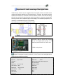
1
Xl2000 development system Shenzhen, China Xuelin Electronics Co., Ltd.
Xl2000
mcu
-1-
development system
Chapter I: XL2000 integrated single-chip simulation Instrument System ... ... .. ... …... ..2
Chapter I I: Quick Start – Follow me to make XL2000 Marquee experiment….. …… ... .5
Chapter III: USB interface installation guide .. ... ... ... ... ... ..... ... ... ... ……... ….. ... ... 10
Chapter IV : Using ISP downloading part . ... ... ... ... ... ... .... ... ... ... .. ………………...13
Chapter V : XL2000 simulating operation guide . ... ... ... ... .... ... ... ... ... ... . ... ….. .. ..17
Chapter VI: XL2000 single chip system Experiments .. ... ... ... ... ..... ... ... ... ... ….. ... 21
pins of MCS-51 single chip .. ... ... ... ... ... ... ... ... ... ... ... ... ... ... ... ... ... ... ...... ... .... . .23
Experiment 1: simple eight-way Marquee case.. ... ... ... ... ... ... ... ... . ... ... ... ... ... .... .. .23
Experiment 2: 8-way controller lantern case with XL2000 experimental system……..... .25
Experiment 3: 8-way DIP switch state display with 8 indicators…….. ... ... ... ... .... ..... ...26
Experiment 4: Digital Tube display with static scanning.... ... ... ... ... ... ... ... ... ….. ... .. ...27
Experiment 5: LED number display with dynamic scanning. ... ... ... ... ... ...…. ... ... ... ... 28
Experiment 6: key button detecting (number show) ………………………………..….. ... ..31
Experiment 7: Matrix keypad recognition technology... ............... ... ... ... ... .… ... ... ... ...32
Experiment 8: 74LS14 reverser experiment ........... ……….... ... .... ... ... ... ... ... ... ... .. .34
Experiment 9: 74LS138 3-8 decoder experiment ... ... ... ... ……….... ... ... ... ... ... ... ... .35
Experiment 10: 74LS164 serial in parallel out control experiment …….... ... ... ... .… ... ..36
Experiment 11: 74LS165 parallel in serial out control experiment... ... ... ... ... ... ...…. ... .37
Experiment 12: D/A conversion experiments with DAC0832………………………….…. . 39
Experiment 13: A/D conversion experiment with ADC0804 ... . ... ... ... ... ... ... .... ... .... ..41
Experiment 14: alarm with small speaker case ….. ... ... ... ... ... ... ... ... ... ... ... ... ... ... . .43
Experiment 15: infrared remote control experiment ... ... . ... ... ... ... ... ... ... ... ... ... ... ... 44
Experiment 16: Chinese characters display case……………………….... ... ... ... .... ... ...47
Experiment 17: 8155 experiment ... ... ... ... ... ... ... ... ... ... ... ... ... ... ... ... ...... ... ... .. ...49
Experiment 18: 24C02 store the number of booting .. .............. ... ... ... ... ... ... .... ... ... ...51
Experiment 19: step motor experiment ......... ... ... .. ... ..... ... ... ... ... ... ... ... ... ... ... ... ...53
Experiment 20: 93c46 demonstration program …………..... ... ... ... ... ... ... ... ... ... ... ... .54
Experiment 21: two-way serial communication experiment... …………….. ... ... ..... ...... .56
Experiment 22: digital temperature display system with 18B20 …………………..….. ... .57
Experiment 23: hardware counter experiment with NE555 oscillator ... …………...... ... .63
Experiment 24: real-time clock experiment with DS1302.. ... ... ... ... ..... ... ... ... ... ... .. ..66
Experiment 25: PS2 keyboard experiment... ... ... ... ... ... ... ... ... . ... ... ... ... ... ... ... ... .. .67
Experiment 26: SD card SPI mode experiment………..... ... ... ... ... ... ... ... ... ... ... ... ... .68
Experiment 27: 485 communication experiment …..... ... ... ... ... ... ... ... ... ... ... ... ... .. ...69
Experiment 28: 12864 LCD display “A”... ... ... ... ... ... ... ... ... ... ... ... ... ... ... ... ... ... . ...71
Chapter VII frequently asked questions and answers ……..... ... ... ... ... ... ...... ... .. ..73
Chapter VIII system configuration and post-sale service guide
... ... ... .. .. .... ... ..75
User survey card ... ... ... ... ... ... ... ... .... ... . ... ... ... ... ... ... ... ... ... ... ... ... ... . ..76
Attention: Whether you're a novice or expert, please spend at least one hour to read this
manual carefully.
Xl2000 development system Shenzhen, China Xuelin Electronics Co., Ltd.
-2-
Chapter I: XL2000 integrated single-chip simulation system
1.1 System
XL2000 comprehensive experimental system (shorts for XL2000) is a multi-functional
8051 MCU development platform (partly supporting AVR/PIC family chips) which is
developed by Xuelin Electronic Co. Shenzhen, China. The company has more than 10
years of experience on embedded system designing and manufacturing around 8051
MCU family chips. XL2000 combines not only the peripheral hardware often seen on
other similar product, also ISP downloading wires, MCU programmer, debugger and
simulator all in one board. With the assistant of hundreds of short and real runnable C
language programming examples, you could learn the programming technology
comprehensively in the shortest time. It is especially suitable for beginners, college
students and embedded engineers.
In particular:
What are the features of XL2000? What can we do with it? It is integrated more than 30
full-opening hardware modules with powerful functionality. You can configure and active
them as you wish.
CP2102 All USB
12846 Chinese LCD
communication
(Optional)
89C2051 The core
1602
Character LCD
monitoring
screen
ADC 0804 Analog - digital
93C46 EPROM
Dac 0832
Digital-Analog
16 * 16, Matrix switch
24C02 Serial EPROM
8-bit LED
74LS165 Into a
8-bit digital tube display
string
74ls138 Decoder
74LS164 Into a
string
74SL47 LED decoding
A relay output
8 DIP switches
Small alarm bell
74LS14 Reverse-
4 button switch
Infra-red remote control
Stepping Motor
NE555 Hardware
button
Single-chip simulation
oscillator
DS1302 Real-time clock
PS2 Experimental
Crystal freedom of choice
keyboard
8155 IOExperimental
expansion'
MAX232 Serial
Communication
Single-chip on-line
programmingISP+ISP
12864 Chinese standard max 485 Communications
sd card modules
LCD
16*16 Chinese dot-matrix Mcp2551 can be reserved 18B20 Digital temperature
screen
bus
collector
The XL2000 features:
1. Entirely open mold designing:
What is the entirely open mode? All hardware resources are open for users. They are not
pre-connected on the board. You can combine various hardware resources into a simple
working embedded system as you wish. You have the most flexibility to configure the
Xl2000 development system Shenzhen, China Xuelin Electronics Co., Ltd.
-3-
hardware and programming on it. For example, when you are writing a marquee program,
you can write P1 port or P2 port without any limitation on the hardware pre-connection.
You only need to change the connecting wires of the system. By this way, you are not
limited by the pre-connection among the hardware resources and have more intuitive
feeling about how the software is controlling the hardware deeply. Actually XL2000 is the
only development board which supports entirely open designing in the market.
2 high-quality technology:
This experimental box employs transparent Jacques power panels, with aluminum alloy
containers, made by machines with surface mount technology. The workmanship is
fabulous.
3. Super powerful hardware resources configuration:
It integrates almost all the possible functional module parts oriented to the real application
of this 8051 MCU. You do not need to find other components and it should be very helpful
for your development task.
4. Perfect sample programming examples:
With more than 10 years of 8051 developing and designing, we are offering programming
examples for each hardware module on the board. In addition to the sample code, we are
also providing step by step instructions, principle pictures and connecting method. We
hope our effort could speed your learning and developing embedded system.
5. USB communication connectors:
USB communication connectors could be used for ISP downloading and also power
supplying. It is not necessary to supply the board with an extra external power. It
facilitates the laptop users who have not LPT or COM port on his laptop. The single wire
connection makes it extremely simple and suit for debugging on the field.
6. anti-plug-protection:
All plugs are designed to prevent wrong plug-in. With connection pictures and clear
instructions, it is convenient for your learning even if you are a beginner.
7. More ISP downloading options:
You could choose either RS232 or USB for the communication between the development
board and the host PC. The communication is controlled by a separate 89C 2051 which
removes the impact on the host PC/OS and improves the stability. The communication
could be used as an independent ISP downloading interface for 51/AVR/PIC family ships.
Also, it could be used as an independent programming interface for 89S51/52 etc. chips.
8. Equipped with 40pin simulator head:
It could be used as an independent simulator for 51 MCU. With the help of KEIL software,
it supports on-line debugging like single step execution, break point and full run.
Xl2000 development system Shenzhen, China Xuelin Electronics Co., Ltd.
-4-
9. Unique intelligent single click design in software:
You can finish the erasing, writing, verification and running by a single click. It is very
helpful for the real programming and reducing the unnecessary debugging time. For
example, by the verification step, you are confident your code is really written into the chip.
So you can locate connection issue or logical issue in the code quickly when there is
something wrong. It is also suitable for international users with our offering of English
software version. It is specially equipped with a 3in 1 public plug which supports burning,
running and simulating. It is convenient and not need to plug and unplug here and there.
System requirements:
WINDOWS98/ME/2000/XP/2003 operation system, if English OS, must be configured
with Chinese character set.
Minimum 50MB space in hard disk.
At least one USB port or RS232 serial port
Step by step learning approach:
When you get this elegant experiment box, please do not hurry power on the board, we
suggest you:
1. Spend about 1 hour to read the manual carefully.
2. Get familiar with various modules built in this experimental box, especially the definition
and intention of wire jumpers.
3. Pick up the example which suits your situation from the handbook to do experiments. If
it could be run smoothly, please think about why this example is written like this. And then
try to change some statements in the program, and then see the result on the board. By
this way, you can have a deep impression how the software is driving hardware acting as
you wish. We believe this is the best way to learn how to program an embedded system.
1.2 Each interface module definition:
Xl2000 development system Shenzhen, China Xuelin Electronics Co., Ltd.
-5-
items
Port
comment
1.communication and
JP14
RS232/USB communication selector(select actual used port)
downloading
JP13
RS232/USB communication selector(select actual used port)
JP17
Programmer/simulator selector(pop on=program, press down=simulator)
K16
Reset. When it is pressed, the program restarts.
JP2
USB communication port, for communication, simulation, programming and power
supply.
JP1
RS232 communication port,exclusive with USB communication, anyway, when use
RS232 communication, also need USB cable to supply power.
JP23
ISP downloading head,support to download program from host PC to board. It
needs basic understanding of the chip will be burned.
2. power supply
JP33
Power switch. It is only applicable for extra power supply. When using USB for
power supply, it is invalid.
J4
3. CPU simulation
IC16
Extra power input.( Default with USB for power supply, no extra power input)
Experimental socket. When programming, insert AT89S52 and simulating with
SST89E564.(attention: make sure the chip breach is up.)
4. Analog to Digit
converter
ADC0804
JP44
P1 output port(P1.0~P1.7)
JP53
P3 output port(P3.0~P3.7)
JP51
P0 output port(P0.0~P0.7)
JP52
P2 output port(P2.0~P2.7)
JP59
40PIN simulator head, same order with standard 8051 pins, take care of pin order
J3
ADC0804 control terminal
JP35
ADC0804 data terminal
JP30
External analog signal input.
JP60
AD jumper. Default state is on, if needing external analog signal, input from AD
input port JP30.
ADJ13
5. Digit to analog
AD experiment. Used for analog signal, adjustable 10K resistor.
JP24
DAC0832 control end, in this system, connect WR to P36, CS to P27
JP27
DAC0832 data end, in this system, connect to P0 port
converter
DAC0832
6. LCD display
12864LCD
7. 8bit digit led
J2
JP41
DAC0832 output end, connect to oscilloscope.
LCD experiment jumper, when doing LCD experiment, make it closed
Note: here we have 12864 LCD.
Xl2000 development system Shenzhen, China Xuelin Electronics Co., Ltd.
JP8
-6-
control end, in this system, connect to P2 port.
JP5
data end, in this system, connect to P0 port.
8. decoder(74LS47)
JP19
74LS47 data input.
JP88
74LS47 data output, in examples, could connect to JP5
9. parallel in serial
JP28
74LS165 data input.
out74LS165
JP21
74LS165 data output.
10. 3-8
JP22
74LS138 data input.
decoder74LS138
JP25
74LS138 data output
11 serial in parallel
JP20
74LS164 data input, in examples, A/B is connected to P3.0, CLK to P3.1.
out74LS164
JP26
74LS164 data output, in examples, connect JP32 to show 8 way output.
12 inverter(74LS14)
JP29
74LS14 data input
JP34
74LS14 data output, change signal from low to high or high to low
JP31
Motor control signal input
JP36
Motor output
14. 93C 46
JP46
93C 46 control
15 24C 02
JP38
24C 02 control, in examples, SLC is connected to P3.6, SDA to P3.7
16 speaker
JP16
Input signal for speaker, in examples , connected to P3.3
17 remote
JP45
Input signal for remote receiver, in examples, connected to P3.7
18 18B20
JP39
Output for temperature detector, in examples, connected to P3.0
20 8way indicator
JP32
Correspond to D00---D07 lights, 0=on, 1=off
21 matrix switches
JP50
Correspond to 4*4 matrix keys, in examples, connected to P1
22 1 way relay output
JP1
Correspond to JP00 relays,
23 DS1302
JP83
in examples, connected to P1.0,P1.1,P1.2
24 NE555
JP80
JP80 OUT W2Adjustment
25 PS2
JP81
TO PC PS2 KEYBOARD
26 Crystal select
JP89
S1 USER ----12MHZ
27 SD CARD
JP74
JP74 CS DI CK DO 5V GND
28 dig switch
JP40
Correspond to J00---J07 dig switches, on=0, off=suspending
29 232 PORT
JP1
TO PC RS 232
30 485 PORT
JP76
J24 A GND B J25 RO.DI .E
31 CAN BUS
JP75
Retention
13 step motor
32. 8155 extension
33 Chinese lattice
JP63 for control, JP58 for data, JP61 for PB port
JP55
Row scan for top half, in examples, connected to P0.
JP54
Row scan for bottom half, in examples, connected to P2
JP62
Column scan, connect to 74LS154.
Xl2000 development system Shenzhen, China Xuelin Electronics Co., Ltd.
-7-
Chapter II: Quick Start – follow me to make XL2000 Marquee experiment
2.1 software installation:
Insert CD shipped with the package, open the driver \XLISP directory. Double-click the
setup.exe, follow the prompts and click next button until the installation is complete. If you
get the remainder that system files are old, probably you need restart your computer and
continue the installation.
First of all, let’s use XL2000 over serial port to do a simple marquee experiment.
① software status information window
② code and data zone:
Show information about the current Show the code/data that is burned into
programmer, status of current connection, chip, also you can edit the code/data directly
serial port, chip and target object file.
here.
③ Intelligent all-steps-in-one button
④ Intelligent button set up window
One of the features of this software, you can Show the status of each step about the
achieve fast programming. Please refer to the whole programming process, includes update
details of the relevant sections.
file, checking chip, erase, write, verification,
encryption, etc.
⑤ file update
Manually updates the target file.
⑥ reset the target board
Pressed the button to reset the target board. It
is helpful for on-line debugging.
⑦ status report on the operation of window ⑧ menu and toolbar
Dynamic display of all the current Short cuts for some menu item.
programming operation.
⑨ progress indicator of the programming
Dynamic display of the current operation
progress.
Xl2000 development system Shenzhen, China Xuelin Electronics Co., Ltd.
-8-
Hardware installation:
Open the package of XL2000, insert the serial line (9 for 9-pin), then plug the USB cable
(for 5V power supply). Press down power switch, and power indicator light is on.
Make sure the following is set up correctly:
•
•
•
Jumpper JP14/JP13 is switched to RS232 end, the other end is USB.
programming/simulation button is in pop-up (programming) state.
CPU is AT89S52 at the cpu socket, and the lock is fastened.
Attention
n
2.2 software
Here are the basic software operations: Double-click the XLISP icon on the desktop to
start the program. At this moment, a serial port option box is popped up. At this point, if
you are not sure which port you can use, please hit "auto detect" button. Or you can select
the COM port as you decided. By default, you can select COM1 port.
(For USB communication, you may need to select COM3 or COM4, refer Chapter III for
the specific USB installation guide) In case of XLISP software unintended termination,
reopen the software: hit the menu options/serial /auto-detection, it is very convenient! )
1 At this point, if the serial port settings are 2 In order to simplify the steps, the software
correct, then there will be the main interface settings should be checked at the first time.
of the following: the status report on the First, click "Settings" button in the toolbar, In
operation of the window display --- the automatic programming options: marked
programmer detecting is OK!
the "Erased", "write" "target board to run" and
If not OK, please check if the COM port then click OK. In generally, detecting chip
settings are correct? Power indicator light is type, checking empty, verification and written
on? The simulation/programming mode is in encryption should not be marked, it is a waste
programming (up) state? USB/232 jumper is of your valuable programming/learning time.
switched to rs232 ? )
Xl2000 development system Shenzhen, China Xuelin Electronics Co., Ltd.
-9-
Attention
3 types of chips dialog box: select 4, the main interface: click the "Open", to find
MCU\ATMEL_51\AT89S52, and then click an exmaple in the CD. For example, test
OK.
cases\...\28LED.HEX, and click OK.
5 At this point, click "smart all-in-one" button, Attention; In the process of programming
and you will see the progress bar of operation, the LED indicator for programming
programming instructions, at the same time, is on, after completing programming, the LED
in status report window, you can see status of will be off. This light, as the programming
each step:
state indicator, is very important! At this point,
Erase staring ....Erase complete.
programming
procedures
have
been
Programming starting ....
completed.
Programming is OK!
Next, the hardware needs to be connected:
Program exiting, and target board is running! As this is a marquee case using P1 port of
89s51, pick one of 8PIN line, insert one end to
the P1 port(JP44) of CPU on XL2000, the
other
end
to
the
eight-way
light
indicators(JP32). We can see the P1 port 8
LED flashes one by one. This shows the
program is running successfully. If it is not
running, press the system reset switch (K16).
Please refer to the related program readme
for other test cases on how to do hardware
connection!
Attention
Xl2000 development system Shenzhen, China Xuelin Electronics Co., Ltd.
- 10 -
Chapter III of the USB interface Installation Guide
XL2000 provides a serial or USB communication for your options. In the above
chapter, we introduced the use of serial communication experiment. If you use the USB
communication, serial lines can be removed. At the same time, please pay attention to
switch jumper JP13, JP14 to USB end.
Please follow below steps to install USB/serial driver
Step one: connect XL2000 to PC USB socket Step two: Select "in the search to include the
by the USB cable in the package: “Found New location", click browsing to open CD and
Hardware Wizard” is showed, select "from the switch to the folder ..\drivers\XLISP drivers\
list or specific location (Advanced)" option, USBDRIVER2.0\, Enter the next step
Enter the next step;
Step three: Pop-up "to install hardware" dialog Step four: The second pop-up system "found
box, If prompts with "did not pass the new hardware wizard" dialog box, Repeat the
Windows logo testing ...", it does not matter. above steps; Pop-up dialog box in the bottom
Click "continue", Started to install wizard right corner "of the new hardware is installed
software; Then pop "Found New Hardware and can be used "USB drive has been
Wizard to complete" dialog box, Click Finish. successfully installed. You can enter the
system:ControlPanel\system\hardware\Devic
e Manager in the following port information,
That the system has been installed in the right
USB drive.
Xl2000 development system Shenzhen, China Xuelin Electronics Co., Ltd.
- 11 -
olution for Failure of installation:
If unintentionally terminate the installation of the software, you can delete the USB device
with yellow exclamation mark and then repeat the above steps to install it again!
USB installation for special case:
Under normal circumstances, the installation of USB is as mentioned above. Under some
special circumstances, your computer may have installed other usb printer, usb
programmer, and so on. In this case, available COM port for USB device maybe COM5 or
COM6. Anyway, KEIL software may only support simulation of COM1, COM2, COM3,
COM4. How do we solve this?
Here's a better solution to this problem:
(Figure 1:When PC configured with many usb
devices, the available COM port maybe Figure 2: right button menu of the COM5
COM5, which is not supported by simulation device, click properties menu item.
software, such as KEIL)
Xl2000 development system Shenzhen, China Xuelin Electronics Co., Ltd.
- 12 -
Figure 3: enter the usb serial port (com5)
property, click the "port settings" and then
"high-level properties". Choose a less often
used COM port, for example, COM3.
Figure 4: System has allocated COM3 for
virtual usb serial port.
(tips for USB COM port can not find when
running XLISP software)
After USB driver installation is complete:
running XLISP.exe, and pop-up a COM
selection dialog box, select one port and click
auto detecting button until one is OK. Same
scenario, when doing KEIL UV2 simulation or
serial port communication experiment, we
must choose the COM port.
Xl2000 development system Shenzhen, China Xuelin Electronics Co., Ltd.
- 13 -
Chapter 4 Using ISP downloading part
4.1 ISP to download part of the presentation
ISP (In-System Programming), means the device on the board can be programmed
directly with end-user code/data, do not need to get the device off from the circuit
board. ISP technology is the development trend for future. The ISP part of XL2000 is
the leading product on the market with traditional programmer’s reliability and
ease-of-use download line. Through the single-chip timing control, RS232 serial
communication solves the problems of parallel port ISP compatibility and reliability.
By introducing the related pins of the ISP download head into the circuit board, we
can program the board online with great speed and convenience.
ISP to download a list of some of the support of the chip:
51 Series single-chip:
AT89S51, AT89S52,
AT89LS8252
AT89S53,
AT89S8252,
AT89LS51,
AT89LS52,
AT89LS53,
AVR Microcontroller Series:
AT90S2323,AT90S2343
AT90S4433,AT90S8535
ATmega16,ATmega16L,ATmega161,ATmega161L,ATmega163,ATmega32,ATmega32L
ATmega323,ATmega323L,ATmega64,ATmega64L
ATmega8,ATmega8L,ATmega8515,ATmega8515L
ATmega8535,ATmega8535L
ATtiny12,ATtiny12L,ATtiny13,ATtiny13L
ATtiny15,ATtiny15L,ATtiny22,ATtiny22L,ATtiny26,ATtiny26L
PIC Microcontroller Series:
PIC16F870,PIC16F871,PIC16F872,PIC16F873,PIC16F874,PIC16F876,PIC16F877,
PIC16F873A,PIC16F874A,PIC16F876A,PIC16F877A
AT24CXX:
AT24C01,AT24C02,AT24C04,AT24C08,AT24C16,AT24C32,AT24C64,AT24C128,AT24C
256,AT24C512
Advantages of ISP download head on XL2000:
1. If you design the product as an open or scalable system, then you need to use this
download line or other download line to upgrade the single chip.
2. Upgrade software version before shipments. Many products may need to fix various
bugs before the delivery to the customer. However, the IC may have been weld to the
Xl2000 development system Shenzhen, China Xuelin Electronics Co., Ltd.
- 14 -
circuit board and can not be removed easily. You can use this download head on XL2000
to update the software online with great convenience.
Several ways to download with XL2000 ISP:
1. Reserve downloading sockets on the target circuit board, by this way, we can download
the software in the chip online.
2. If you have not reserve any download socket for the download head, and want to use
XL2000 ISP, in this case, you can make a download head yourself with bare lines and
weld it to the target board.
4.2 Definition for XL2000 download head ( Read below table carefully and
make sure you totally understand it before using!)
1 NC(Vacant)
2 NC(Vacant)
3 NC(Vacant)
4
+5V
6 NC (Vacant)
7 SCK/SCL
8 MISO/SEN/WP 9 MOSI/SDA
5 GND
10 RST
The
order
direction
of The pin definition on the The plug (1) there has a
downloading head is same as board is 1-1 mapping with triangular symbols, make sure
other chips, anti clockwise downloading head.
to avoid pick the wrong line.
direction.
Tips: if you are still not sure the order of pins, better have a check with multi-meter after
connecting.
Special attention:
The pin 4/5 of the downloading head is already provided with +5 power supply, therefore,
there is no need to configure a power for the target board. At the first use of the
downloading head, please check if the power is not short-circuit on the board? As well as
if the pins of ISP is connected correctly? You can refer following to connect the ISP
downloading head:
http://www.51c51.com/bbs/dispbbs.asp?boardID=19&ID=28470&page=1
In addition, because of the use of the downloading functionality of S51 series of single
ship part of software XLISP, make sure there is no chip in the socket of XL2000 when
using the downloading head.
4.3 ISP pin connection method with typical chip
Here are some ISP pin connection methods with a typical chip.
Please refer to chapter two for the software operations.
Xl2000 development system Shenzhen, China Xuelin Electronics Co., Ltd.
- 15 -
AT89S Series, AVR family connection method (refer to the self-made 89S51 target
board)
Download<----->Single-chip goal
RST <------->RST
MOSI <------->MOSI
MISO <------->MISO
SCK <------->SCK
VCC <------->VCC
GND <------->GND
1. AT89S8252 has internal data EEPROM, can do on-line programming.
2.Requirement for a simplest target board system: Crystal (4MHz above), target MCU, 5V
power supply (for the target board and programmer with downloading functionality).
3. Better make the functionality of ISP pins of target single-ship exclusively when
designing the board, do not multiplex with other functionality.
4. If reset circuit is composed of RC circuit, then the RESET pin could be connected
directly. Kindly reminder: the secure capacitance for MCU can not be too high.
Recommend value maybe 1uF, better not exceed 10uF.
Connecting method for PIC series: refer chip manual for PB7, PB3, PB6 definitions,
different PICs may be different.
Xl2000 development system Shenzhen, China Xuelin Electronics Co., Ltd.
- 16 -
ISP downloading<----->target single-chip
RST <------->Vpp(/MCLR)
SDA <------->DATA(PB7)
SEN <------->PGM(PB3)
SCK <------->CLOCK(PB6)
VCC <------->VCC
GND <------->GND
AT24CXX series of ways to connect
ISP download<----->AT24CXX
RST <------->RST
SDA <------->SDA
WP <------->WP
SCK <------->SCK
VCC <------->VCC
GND <------->GND
Xl2000 development system Shenzhen, China Xuelin Electronics Co., Ltd.
- 17 -
Chapter V XL2000 simulation step guide
5.1 Overview: The simulation functionality of XL2000 is implemented by the
simulation module. Through the cooperation with KEIL software, we can support both for
on-board resources simulation, but also can support simulation of external target board
resource by 40PIN ISP downloading head.
•
Simulation can be 89C51, 89C52, 89S51, 89S52, 89C58 microcontroller with 51 core,
and so on.
•
•
Directly support KEIL C51 IDE simulation environment.
USB/RS-232 communication interface, adaptive baud rate 4.8 Kbps-57.6 Kbps.
Especially for laptop users without any RS-232 interface.
•
•
•
Monitor program takes up few resources, if run at full speed, take up no resources.
63K program space inside the chip, can be updated online at any time.
Support single-step, breakpoint, full-speed, variable reference, RAM variables, etc.
debugging.
•
•
Support assembly, C language and mixed source debugging.
Simulation interface on board can be connected to any type of target board, so as to
achieve unlimited hardware simulation of the expansion.
Hardware installation: first of all, connect the 9-pin serial port plug into the PC serial
port, like COM1. Connect usb cable to PC as the power supply, Insert the simulation chip
(not at89s51) into the socket on board and fasten the socket. Press down JP17
(programming / simulation button) and make the board work in simulation mode. (NOTE:
here it is run with serial port, if by USB, then insert the USB line, at the same time make
sure JP13, JP14(232/USB) is switched to USB end) If simulating on-board resources, first
of all, connect the pin lines to the related IO hardware port according to the experimental
objective. The simulation result will be shown directly on the XL2000 board.
If you need simulate a external target board,
connect the simulation head into the target
board, then the simulation result will be
shown on the target board.
Please pay attention to the insertion
direction!
Xl2000 development system Shenzhen, China Xuelin Electronics Co., Ltd.
- 18 -
Software installation: copy cdrom\Tools\keil\ to the root of the c disk,
remove read-only attribute of all files.
(ATTENTION: must be under c root directory)
Execute keil\uv2\uv2.exe, you can create a shortcut for uv2.exe as you wish. (Uv2 icon)
5.2 Create your first project (software operation guide):
2 create assembly source file: Click FILE
(file) menu, NEW ... (new file) to open a new
text editor window, at the blank part, input one
1 Click Project (the project) menu, Select example program like marqueen LEDs. And
New Project, In the "File Name" Enter your then click FILE (file) menu of SAVE (Save)
first name of the project, let us assume it as command to save the file, MUST save the file
"test". "Save" the file with extension .uv2, this with suffix .asm, for example: c:/ 001.asm.
is the KEIL uVision2 project file extension. (Note that do not save the file under some
After that we can directly click the file to open directory with non-ascii characters. Better
the whole project.
save the file under some standard DOS
Then pop-up a dialog box, it will let you directory, at least 8 ascii char, no space in it.)
choose single chip models, let’s choose
ATMEL --- AT89C51. Note that the actual use
of the 89s52, they are totally compatible, do
not have to bother.
Xl2000 development system Shenzhen, China Xuelin Electronics Co., Ltd.
3. Click on "+" in front of the Target 1
- 19 -
4. Simulation part is using Mon51 protocol,
menu, then Source Group 1(Source group prior to use it, project must be set as follows:
1), right-click to select "Add files Group Click the "Project" (the project) menu, In the
Source Group 1" (source documents to be drop-down menu click "options for target 1,
added into group 1) , at this moment, choose click "Target" (the target), enter the simulator
the type of file for Asm, select 001, then Add, frequency (12MHz).
in the prompt box, click "OK".
5. Select output (output) "Create HEX
6.
"Debug"
(debug),
click
on
file" (generate a hex file) option, so that HEX
file could be generated after assembling.
"KeilMonitor-51 Driver", at the same time,
select load the code to the emulator, run to
main0, and then click Set
7 Click "Settings" to choose to use the serial
port(must match with the actual situation,
your computer may be COM2 or other). If
you are not sure this, you can view Control
8. Press down below two small icons to
Xl2000 development system Shenzhen, China Xuelin Electronics Co., Ltd.
- 20 -
Panel \ hardware \port\communication port compile, (Or press F7). After the success of
to solve it. At the same time, pay attention the compilation, you can see text like “0
to not run other software may occupy the error(s), 0 warning(s)…” as the red arrow
COM resources. Serial port debugging shows. At this time, a hex file has been
software must be closed, else may cause generated and we can burn it into a single chip
conflict. (If you are using a USB with ISP downloading. Then we can do
communication, then please select the hardware simulation, connect simulation
virtual serial port number that allocated by module into on-board socket and press down
the system.)
the RESET button on the board.
9, Press the third red d(debug) icon or
ctrl+F5 to enter the simulation.
At this point, the interface shows connection is
successful! (Or there is some wrong with
settings, please double-check)
(Successful simulation screen.)
Click the "running at full speed" button as the red arrow points and connect experimental
resources. This experiment connects the P1 (JP44) of the CPU
to the eight-way indicator lights (JP32) by a 8PIN data cable.
At this time you will see eight XL2000 red LED is flashing one by
one, this means the success of the experiment.
When exiting the simulation, press down the RESET button of XL2000, and then click d,
the IDE will return to the editing mode. Press down the red d again, back to simulation
mode.
Up to here, we have completed a standard KEIL software process. You can hit single-step
running to watch the change of register and also change of the board. By this way, you
can understand the process of the program running. Note: when enter and exit
simulation mode, please press down the RESET button of XL2000.
Xl2000 development system Shenzhen, China Xuelin Electronics Co., Ltd.
- 21 -
MCS-51 single-chip pin description
51 Series single-chips like 8031, 8051 and 89c51/89s51 are all adopting dual in-line
package(DIP) with 40Pins. The following are specifications of the 40pins chart. Power and
ground occupy two pins, external quartz oscillator clock occupy another two pins, total of
32(4*8bit) I/O ports occupy 32pins, the interrupt port multiplexed with P3 port. Next, let us
explain the functions of each pin one by one:
PIN20: ground.
PIN40: +5 V power supply.
PIN19: XTAL1 clock, on-chip oscillation circuit input.
PIN18: XTAL2 clock, on-chip oscillation circuit output.
8051 can work in two clock mode, one is the on-chip
clock oscillation mode, in this case, PIN18 and PIN19
need to be connected to an external quartz crystal
(2-12MHz) and oscillation capacitor. The oscillation
capacitor value takes 10p-30p. Another mode is the
external clock, XTAL1 connected to ground, external
clock signal connected to XTAL2.
Input and output (I / O) pins:
PIN39-PIN32: mapped to P0.0-P0.7 I/O port.
PIN1-PIN8: mapped to P1.0-P1.7 I/O port.
PIN21-PIN28: mapped to P2.0-P2.7 I/O port.
PIN10-PIN17: mapped to P3.0-P3.7 I/O port.
PIN9: RESET/Vpd reset signal. When power on
8051, clock circuit starts to work and a high TTL of
24 clock cycles signal occurs on RESET pin. By this
way, the system is reset and initialized.
The 8051 can be reset automatically and can also
be manually, see below. In addition, RESET/Vpd is a
multiplexed pin, during the Vcc power-down period, this pin can be connected to a
back-up power and make the RAM data inside the chip not lost.
PIN30: ALE/PROG, when the CPU accesses external program, ALE (address latch) used
to latch the output of low-bytes of the address. When CPU accesses internal memory,
ALE will emit a pulse signal of 1/6 clock cycle. This signal can be used to identify whether
the CPU works or not, and can also be used as an external clock output. When writing
EPROM, RROG pin will be used as input programming pulse.
Xl2000 development system Shenzhen, China Xuelin Electronics Co., Ltd.
- 22 -
PIN29: when accessing external program memory, this pin generates negative pulse
selection signal. PC's 16-bit data address will appear at the P0 and P2 port. External
program memory will put instruction at port P0. It is read by the CPU and executated.
PIN31: EA/Vpp, internal and external memory selection pin. 8051 and 8751 single-chip
has built-in 4KB code memory. When EA is high and instruction address is less than 4KB,
CPU loads instruction from internal memory, if instruction address is greater than 4KB,
CPU loads instruction from external code memory. However, when EA is low, CPU always
loads instruction from external memory regardless of address value.
Icon explanation:
beginning of each chapter
Source program of experimentLine
connect
experiment
of
the
Xl2000 development system Shenzhen, China Xuelin Electronics Co., Ltd.
- 23 -
Chapter VI of the single-chip experiment with examples
Limited by the space of this manual, here we provide several typical c51 application
examples. To facilitate the novice to learn programming C51, we will show the source
code, running photo, line connection method and principle schema for each examples. Of
course, XL2000 is not limited by the examples presented here, thanks for the module
design of this experimental instrument, user can configure the hardware modules with
most flexibility and program against the configuration. By this way, user can have a
comprehensive of C51 programming and designing.
For more asm and C sources, please refer to the examples in the CD shipped with the
package, as well as the latest update at: www.8951.com!
Experiment 1: The simplest eight way marquee program
In this experiment, delay subroutines, clr, lcall, ajmp instrunctions will be used. Over these
program elements, we can see eight lights flashing in turn through P1.0 to P1.7 port. User
can learn from this example and have a initial grasp of the IO port programming.
Practice 1: How to make the time of delay subroutine a bit shorter or longer?
Practice 2: How to use P0, P2 and P3 ports to implement the same control of 8-way lights?
Practice 3: how to implement different patterns in the light flashing?
Related schema:
Xl2000 development system Shenzhen, China Xuelin Electronics Co., Ltd.
- 24 -
reference program:
org 0000h
;start
clr p1.5
ajmp LOOP; jump to LOOP label
lcall delay
org 0080h; get to 0030h to reserve some space
clr p1.6
LOOP:
lcall delay
mov p1,#0ffh; turn off all lights
clr p1.7
clr p1.0
lcall delay
;turn on light at p1.0
;
;
;
lcall delay ;delay for a while
AJMP LOOP; jump to LOOP and restart to run
clr p1.1
delay:
;turn on light at p1.1
lcall delay
clr p1.2
d1: mov r6,#40
;
d2: mov r7,#248
lcall delay
clr p1.3
djnz r7,$
;
djnz r6,d2
lcall delay
clr p1.4
lcall delay
mov r5,#20 ; delay number。
djnz r5,d1
;
ret
end
Connection methods: connect P1 port (JP44) of the CPU with eight-way lights(JP32)
with one 8PIN cable. The connecting and program running photo like below: (8 lights turn
on/off one by one).
Xl2000 development system Shenzhen, China Xuelin Electronics Co., Ltd.
- 25 -
Experiment 2: Control Relay
In the relay module, a PNP three tube 2N5401 is used to drive the 5V relay. The relay
touch point is routed out by the JP00 terminal. When the relay does not act, the terminal is
open. When the relay is active, the terminal is closed. Leading the touch point out could
control external device, such as lanterns and so on. It should be noted that control current
should not exceed 1A, the voltage should not exceed 120V. If using the touch point to
control high voltage, be careful!
Input 8way marquee program above.
connect P1.0 of P1 port(JP44) of the CPU to JP18 of relay part, you can hear the
sound of relay’s open/close. Wired the terminal out, you can control the extern lanterns.
The connect photo is like below:
XL2000
running photos
Xl2000 development system Shenzhen, China Xuelin Electronics Co., Ltd.
- 26 -
Experiment 3: 8-way lights showing the status of 8-way DIP switch
One end of 8-way DIP switch is connected to ground, and the other side could be wired
out through JP40, the related schema graph is like below:
The purpose of the experiment: by setting different DIP switch status and let the 8-way
lights indicates the status of 8-way DIP switches. By this way, you can understand the
concept of bits and data transfer in the single chip.
Reference program:
org 0000h ;Start
ajmp
loop
org 0080h
;0030h to the Department of between 00-30 to avoid sensitive Address
loop: MOV A,P0; I P0 state (switch) read A
MOV P1,A
;A data sent to the port P1 (light)
JMP LOOP
;A fresh start
END
Eight-way DIP switches to JP40 with a 8PIN data cable into the CPU of the P0 I
JP51,8PIN and then use a data cable to the CPU part of the P1 I (JP44) connected to the
eight-way part of the light JP32.
The result: Data photo map, corresponding to the switch to open, corresponding to the
bright lights.
XL2000 running photos
Xl2000 development system Shenzhen, China Xuelin Electronics Co., Ltd.
- 27 -
Experiment 4: static scanning of the digital tubes
74LS47 chip is a driver chip of 7-segment tube, the number could be converted to the
numbers that directly displayed in LED tubes through it. Therefore, the program could be
simplified and also the IO resources could be reduced. However, from the cost saving
point of view, such kind of chips have less used in the market. In most cases, dynamically
scanning tube is used to implement digit number display. From students’ perspective, it is
necessary to understand this type of IC application.
The following is the connection diagram for 74LS47:
Connection method: connect the decoding
part of the digital tubes (JP19) to P1
port(JP44), that is P1.0/P1.1/P1.2/P1.3 etc.
XL2000 running photos
Program: this program is sending number 0,1,2,3 to P1 port in turn and digital tube is
showing these numbers accordingly.
org 0000h
; start
CALL DELAY
ajmp loop
; jump to 0030h
JMP LOOP
org 0080h
;
DELAY: MOV R5,#50 ;delay subprogram
LOOP:
MOV P1,#1
D1: MOV R6,#40
; set 1 to p1 port
D2:MOV R7,#248
CALL DELAY ;delay
DJNZ R7,$
MOV P1,#2
DJNZ R6,D2
CALL DELAY
;set 2 to p1 port
;delay
DJNZ R5,D1
MOV P1,#3
RET
CALL DELAY
END
MOV P1,#4
;restart
Xl2000 development system Shenzhen, China Xuelin Electronics Co., Ltd.
- 28 -
Experiment 5: Digital tubes display 01234567 dynamically
Schema graph: data cables of 8 lights are bundled into JP5, the bit control is driven by 8
PNP triode and wired out from JP8.
How the digital tubes display numbers like 1,2,3,4? The digital tubes in fact consist of 7
segment tubes with shape ‘8’ plus a decimal point. We names them as A, B, C, D, E, F, G,
H.
After understanding the display principle, if we want to show a figure ‘2’, turn on the A, B,
G, E,D tubes will do. From the hardware connection, we can program as follow: (we have
several 7-segment tubes, let us assume last one P2.7)
LOOP:
CLR P2.7
SETB P0.7
SETB P0.5
SETB P0.1
CLR P0.2
CLR P0.3
CLR P0.4
CLR P0.6
;Finally, select the digital control
;Section B does not shine
;Decimal point does not shine
;C-section do not
;Other all
Xl2000 development system Shenzhen, China Xuelin Electronics Co., Ltd.
- 29 -
CLR P0.0
JMP LOOP ;Jump to re-start
END
After compiling and burning this program into single-chip, we can see the figure ‘2’ is
displayed on the digital tubes. Maybe you feel it is too cumbersome to write a so long
program and display only a figure ‘2’. As we can see from above, showing figure ‘2’ is
equal to trun off tube C, F and H. Due to the common-anode connection, that means
0(low TTL) is on and 1 is off. From the most bit to least, P0.7~P0.0 could be wrote as
01111110, the hex number is A2H. We can compute this hex number before programming
and store these data into a table. After this, we can call it to display the figure easily.
Show
p0.7 /C p0.6/E
p0.5/H
p0.4/D
p0.3/G
p0.2/A p0.1/F p0.0/B
HEXCod
e
0
0
0
1
0
1
0
0
0
28H
1
0
1
1
1
1
1
1
0
7EH
2
1
0
1
0
0
0
1
0
A2H
3
0
1
1
0
0
0
1
0
62H
4
0
1
1
1
0
1
0
0
74H
5
0
1
1
0
0
0
0
1
61H
6
0
0
1
0
0
0
0
1
21H
7
0
1
1
1
1
0
1
0
7AH
8
0
0
1
0
0
0
0
0
20H
9
0
1
1
0
0
0
0
0
60H
With this table, the displaying of figure ‘2’ could be simplified to:
LOOP:
CLR P2.7
; select the digital tube on the left side
MOV P0,#0A2H ; send the hex number of 2 to P0 port
JMP LOOP
; Jump and restart
END
( running photos)
1. connect data port(JP5) of digital tube to P0 port(JP51) of CPU.
2. connect display port(JP8) of digital tube to P2 port(JP52) of CPU.
Xl2000 development system Shenzhen, China Xuelin Electronics Co., Ltd.
ORG 0000H
AJMP
MAIN
ORG
0080H
MOV
P0,#74H
LCALL
DELAY
MOV
MAIN:
P2.4
CLR
P2.0
MOV
P0,#28H
; display ‘0’
MOV
P0,#61H
LCALL
DELAY
; call delay
LCALL
DELAY
MOV
P0,#0FFH
MOV
P0,#0FFH
SETB
; select 1 digital tube
; turn off ‘0’
P2.0
CLR
P2.1
MOV
P0,#7EH
LCALL
MOV
SETB
P2.1
CLR P2.5
;
SETB
; select 2nd digital tube
P2.5
CLR
P2.6
MOV
P0,#21H
DELAY
LCALL
DELAY
P0,#0FFH
MOV
P0,#0FFH
SETB
P2.6
; select 3 digital tube
CLR
P2.7
;display ‘3’
MOV
P0,#7AH
LCALL
DELAY
; display ‘1’
rd
;
CLR
P2.2
MOV
P0,#0A2H
LCALL
DELAY
MOV
P0,#0FFH
SETB
P2.7
SETB
P2.2
MOV
P0,#0FFH
CLR
P2.3
AJMP
MAIN
MOV
P0,#62H
LCALL
DELAY
MOV
P0,#0FFH
SETB
CLR
;
; display ‘3’
;
DELAY:
MOV R6,#25
D2:
DJNZ
DJNZ
END
;
;restart
;delay subroutine
D1:
RET
;
;
MOV R7,#2
P2.3
P2.4
;
P0,#0FFH
SETB
st
- 30 -
R6,D2
R7,D1
Xl2000 development system Shenzhen, China Xuelin Electronics Co., Ltd.
- 31 -
Experiment 6: port button press detecting technologies (display button)
This part consist of 8 touch keys, one end to the ground, the other end is wired out from
JP48. When press the key, the corresponding port is low TTL.
Key port schematic
Connection methods:
1. connect JP48 to P3 port(JP53) of CPU by a 8pin cable.
2. connect data port(JP5) of the digital tube to P0 port(JP51) of the CPU.
3. connect display port(JP8) of the digital tube to P2 port(JP52) of the CPU.
Task: display 0,1,2,3 by pressing K02, K03, K04, K05 keys.
org 0000h;(1)
ljmp start;(2)
l2:
org 0080h;(3)
start:
mov p0,#28H
;display '0';(12)
l3:
mov p0,#7EH ;display '1';(14)
l4:
mov p0,#0A2H ;display '2';(16)
CLR P2.6 ;select most right digital tube;(5)
l1:
; checking in loop(11)
ljmp l1;(13)
mov p2,#0ffh;(4)
mov
ljmp l1
p3,#0ffh
;initialize P3 port(6)
jnb
p3.2,l2
;(7)
jnb
p3.3,l3
; ;(8)
jnb
p3.4,l4
; ;(9)
jnb
p3.5,l5
; check key pressing(10)
ljmp l1;(15)
ljmp l1;(17)
l5:
mov p0,#62H
ljmp l1;(19)
end;(20)
;display '3';(18)
Xl2000 development system Shenzhen, China Xuelin Electronics Co., Ltd.
- 32 -
Experiment 7: Matrix key recognition technology
Matrix key part consists of 4*4(16) keys and it is connected to JP50 port. The I/O port
connected by row lines are outputs, and the I/O port connected by column lines are inputs.
When no key is pressed down, all the outputs are high TTL. Once a key is pressed down,
the input line is low TTL, we can read the corresponding port to know if any key is pressed
down.
The following gives a specific example:
The purpose of the experiment:
corresponding key is down.
show 0,1,2…A,B,C,D,E,F on digital tube when
Connection methods:
1. connect matrix key JP50 to P1 port(JP44) of the CPU.
2. connect data port(JP5) of digital tube to P0 port(JP51) of the CPU.
3. connect display port(JP8) of digital tube to P2 port(JP52) of the CPU.
Reference:
org 0000h
L3: JB P1.3,NEXT
ajmp main
;
MOV A,#0cH
org 0080h
LK: ADD A,R4
main:
;
;
PUSH ACC
mov dptr,#tab ;put tab at DPTR
lcall key
;call matrix key detecting
program
movc
K4:
;
LCALL DELAY2
;
LCALL KS
;
JNZ K4
a,@a+dptr
;load tab data to
ACC
POP ACC
RET
mov p0,a
;move ACC to PO port
CLR P2.1
;open display on P2
ljmp main
KEY: LCALL KS
JNZ K1
LCALL DELAY2
;display in a loop
NEXT:
INC
R4
;add 1 to column value
MOV A,R2
;
;call key detecting
JNB ACC.7,KEY ;
;if key is down, continue
RL A
;no key down, call
;
MOV R2,A
;
Xl2000 development system Shenzhen, China Xuelin Electronics Co., Ltd.
delay to remove shaking
AJMP K3
AJMP KEY ;get back to continue detecting
K1:
KS: MOV P1,#0FH
LCALL DELAY2
; call delay to remove
;
RET
LCALL KS
;call key detecting
JNZ K2
DELAY2:
;
;
K2: MOV R2,#0EFH
L8: DJNZ R6,L8
st
;move 1 column to R4
K3: MOV P1,R2
DJNZ R5,L7
; move R2 to P1 port
;
MOV A,#00H
RET
tab:
;
AJMP LK
db 28h,34h,28h,34h,0a9h,60h,20h,7ah,
;
L1: JB P1.1,L2
20h,21h,61h,74h,30h,62h,0a2h,7eh
;
MOV A,#04H
end
;
;
L2: JB P1.2,L3
MOV A,#08H
;
L7: MOV R6,#0FAH
;store key value to R2
MOV R4,#00H
;
MOV R5,#08H
AJMP KEY
;
;send 3rd row value to
ACC
AJMP LK
;
XRL A,#0FH
shaking
L6: JB P1.0,L1
;
MOV A,P1
LCALL DELAY2
AJMP LK
;
;
- 33 -
Xl2000 development system Shenzhen, China Xuelin Electronics Co., Ltd.
Experiment 8:
- 34 -
74LS14 reverser
74LS14 is a 6way reverser, the definition of pins as left figure:
A for input, Y for output, that is,
pin 1,3,5,9,11,13 for inputs, pin 2,4,6,8,10,12 for outputs.
In this instrument, two 74LS14 chips are used to consist of a
8-way reverser.
Experiment: 8-way adder, through reverser to see changes on LED outputs.
org 0000h
delay:
mov r5,#50
ajmp main
d1: mov r6,#40
org 0080h
d2: mov r7,#248
main:
mov a,#0
djnz r7,$
loop:
mov p1,a ; P1 port output
djnz r6,d2
call delay ; keep on for a while
djnz r5,d1
inc a
ret
; show next figure
jmp loop
;call delay
end
Connection methods:
1: direct connection: connect 8way 2:
reverser connection, connect P1
indicators(JP32) to P1 port(JP44) of CPU by port(JP44) of CPU to the inputs(JP29) of the
a 8pin cable.
reverser by a 8pin cable. Connect reverser
At this point, we can see the lights are outputs(JP34) to 8-way indicators(JP32).
turned off as binary sequence.
At this point, we can see the lights are
turned on as binary sequence.
Xl2000 development system Shenzhen, China Xuelin Electronics Co., Ltd.
- 35 -
Experiment 9: 74 LS138 part of the 38 decoder part of the experiment
The 3-8 decoder is used to control 8 lines through 3 lines. In the circuit, it plays a role of
extending IO resources.
74LS138 Pin definition
74LS138 Logic table
74138The circuit schematic
Following experiment is a 8-way marqueen program through 74LS138, the 3 way
inputs are P1.0, P1.1 and P1.2.
Connection method:
1. connect inputs(JP22) of 74LS138 to P1.0~P1.3(JP44) of CPU by a 4pin cable.
2. connect outputs(JP25) of 74LS138 to 8-way indicators(JP32).
org 0000h
ajmp main
org 0080h;
AA EQU P1.0
BB EQU P1.1
CC EQU P1.2
MAIN:
CLR CC
;
CLR BB
CLR AA
CALL DELAY ;
CLR CC
;
CLR BB
SETB AA
CALL DELAY ;
CLR CC
;
SETB BB
CLR AA
CALL DELAY
CLR CC
SETB BB
SETB AA
CALL DELAY
SETB CC
CLR BB
CLR AA
CALL DELAY
SETB CC
CLR BB
SETB AA
CALL DELAY
SETB CC
SETB BB
CLR AA
CALL DELAY
SETB CC
SETB BB
SETB AA
CALL DELAY
JMP MAIN ;
DELAY:
MOV R5,#255
D3:MOV R2,#255
D4: DJNZ R2,D4
DJNZ R5,D3
RET
END
Xl2000 development system Shenzhen, China Xuelin Electronics Co., Ltd.
- 36 -
Experiment 10: 74LS164 serial in parallel out
In a single-chip system, if the parallel I/O port resources is not enough, and the serial port is free and not
occupied, then we can use a 74LS164 to extend parallel IO port. 74LS164 is a shift register of serial in
parallel out and equipped with clear terminal. Among the pins, Q0-Q7 are parallel outputs. A, B are serial
inputs. MR is for clearing, 0 for clear output. CP is clock input.
74LS164 Pin definition
74LS164 Logic table
74LS164 Circuit
Connection methods:
1. connect P3.0/P3.1(JP53) of CPU to inputs(JP20) of 74LS164 with a 2pin cable.
2. connect outputs(JP26) of 74LS164 to 8-way indicators(JP32) with a 8pin cable.
The following program: 8 way marqueen through 74LS164.
org 00h
DELAY: ;
jmp start
MOV
org 0080h
D3:MOV R2,#255
mov scon,#00000000b
;set UART to MODE0
R5,#255
D4: DJNZ R2,D4
start:
DJNZ R5,D3
mov dptr,#table ;set data pointer to the TABLE
RET
loop:clr a
table : db 01h,02h,04h,08h
;clear ACC
movc a,@a+dptr
cjne a,#03,a1
;get data from TABLE
;
;
a1: cpl a
db 10h, 20h,40h,80h
;reverse the data
mov 30h,a
;store ACC at 30H
mov sbuf,30h
;
loop1:jbc ti,loop2 ;
jmp loop
db 80h,40h,20h,10h
;right shift
db 08h, 04h,02h,01h
db 80h,40h,20h,10h
db 08h, 04h,02h,01h
jmp loop1
inc dptr
db 10h, 20h,40h,80h
db 01h,02h,04h,08h
jmp start
loop2: call delay
;left shift
;
;
db 00h,0ffh,00h,0ffh
db 03h
;
END
;
Xl2000 development system Shenzhen, China Xuelin Electronics Co., Ltd.
- 37 -
Experiment 11: 74LS165 parallel in serial out
74L165 is a shift register with parallel input serial output. The serial port internal 80C51
works under mode 0. The parallel I/O port could be extended by shift register chip.
The definition of pins:
A, B, C, D, E, F, G, H: parallel input.
QH: serial output.
CLOCK: clock input.
CLOCK INHIBIT: clock disable. High TTL is valid.
SHIFT / LOAD: shift and set control
SER: expand multiple 74LS165 connected by head/tails.
74LS165 pin definition
74LS165 logic table
74LS165 circuit:
Connection methods:
1. connect P3.0~P3.3(JP53) to inputs(JP21) of 74LS165 with a 4pin cable.
2. connect outputs(JP28) of 74LS165 to 8way button switches(JP48) with a 8pin cable.
3. connect P1 port(JP44) of CPU to 8way indicators(JP32).
Press down k00~k07, we can see d00~d07 are under control.
Xl2000 development system Shenzhen, China Xuelin Electronics Co., Ltd.
XL2000 running photos
reference program:
org 0080h
delay:
loop : mov scon,#00010000b ; set MODE=0
clr p3.2
call delay1
; P3.2=0 to load data
;
;P3.2=1 to output
clr ri
;RI=0
;
djnz r6,$
ret
delay1:
mov r7,#02
jmp loop1
;
loop2:mov a,sbuf
;
mov p1,a
; output P1
jmp loop
mov r6,#00h
djnz r7,tt
setb p3.2
loop1:jbc ri,loop2
tt:
mov r7,#00h
; restart
djnz r7,$
ret
end
- 38 -
Xl2000 development system Shenzhen, China Xuelin Electronics Co., Ltd.
- 39 -
Experiment 12: DA conversion and application of the principle of dac0832
DAC0832 is D/A converter chip with 8-bit resolution, fully compatible with the processor,
and it has the advantage of low cost, simple interface and easy conversion control. It is
widely used in single-chip system application.
(1) the pin and functionality of DAC0832
DI0~DI7:data input line, TLL level.
ILE:latch data lines to allow input control
signals, HIGH is valid.
CS:selection input line, LOW is valid.
WR1:write selection input signal of input
register
XFER:input control line of data transmission,
LOW is valid.
WR2:write selection for DAC register.
Iout1: current output line, when all inputs are
all ‘1’, Iout1 is largest.
Iout2: current output lines, the sum of its
value and Iout1 is a constant.
Rfb: input signal feedback, there is an internal
feedback resistor in the chip.
Vcc: power input (+5 v ~ +15 v)
Vref: baseline voltage input (-10v ~ +10 v)
AGND: analog ground for the analog signal
and baseline voltage.
DGND: digital ground.
DAC0832 Experimental schematic:
Xl2000 development system Shenzhen, China Xuelin Electronics Co., Ltd.
- 40 -
Reference: trapezoidal wave generated by DAC0832.
ORG 0080h
next :
MAIN:
ADD A,#10 ;increase gradient of 19H
mov a,#0
MOV DPTR,#07FFFH
MOV R1,#0ah
sjmp lp
DELAY:
;
LP: MOVX @DPTR,A ;address selection
D2: MOV 31H,#0FFH
ACALL DELAY ;
D1: DJNZ 31H,D1
djnz r1,next
RET
sjmp main
END
Connection methods:
1. connect P3.6(JP53) of CPU to WR of DAC0832(JP24) with 1pin line
2. connect P2.7(JP52) of CPU to CS of DAC0832(JP24) with 1pin line
3. connect P0(JP51) of CPU to data input of of DAC0832(JP27) with 8pin line
4. observe the converted signal at J2 by an oscilloscope. Suggest adjust Y axis to
0.2V/cell, X axis to 1MS/cell.
Oscilloscope waveform output photos:
Xl2000 development system Shenzhen, China Xuelin Electronics Co., Ltd.
Experiment 13:
- 41 -
A / D converter ADC0804
The so-called A / D converter is the analog/digital converter (Analog to Digital Converter referred to as
ADC) whose functionality is to convert analog signals into digital signals.
ADC0804 specifications and pin definitions
/CS:chip select signal.
/WR:Used to start the conversion of control. When
VREF:Auxiliary reference voltage.
/WR from HI to LO, the converters have been
cleared; when /WR back to the HI, the conversion
starts;
/RD:external converter to read the results of the foot DB0~DB7:8-bit digital output.
control output signal.
/INTR:Interrupt request signal output, low-level
AGND,DGND:Analog and digital signal grounding
action
:Differential analog input voltage.
CLK IN,CLK R:Then the clock input or oscillation VIN(+),VIN(-)
component (R, C), about restrictions on the
Single-ended input voltage, VIN (-) grounding;
frequency of 100KHz ~ 1460KHz
VCC: power supply, as a reference voltage of circuit.
voltage input and digital output relations for ADC0804 as shown in the table
Hex
Binary code
And the ratio of full scale
The relative value of the electricity
should be VREF = 2.560 V
Four high-byte
Four low-byte
Four high-voltage The four l
bytes
ow-voltage bytes
F
1111
15/16
15/256
4.800
0.300
E
1110
14/16
14/256
4.480
0.280
D
1101
13/16
13/256
4.160
0.260
C
1100
12/16
12/256
3.840
0.240
B
1011
11/16
11/256
3.520
0.220
A
1010
10/16
10/256
3.200
0.200
9
1001
9/16
9/256
2.880
0.180
8
1000
8/16
8/256
2.560
0.160
7
0111
7/16
7/256
2.240
0.140
6
0110
6/16
6/256
1.920
0.120
5
0101
5/16
5/256
1.600
0.100
4
0100
4/16
4/256
1.280
0.080
Xl2000 development system Shenzhen, China Xuelin Electronics Co., Ltd.
- 42 -
3
0011
3/16
3/256
0.960
0.060
2
0010
2/16
2/256
0.640
0.040
1
0001
1/16
1/256
0.320
0.020
0
0000
0
0
reference program
nop
; ADC0804 reference program:
//define ADC PORT
nop
ad_cs
equ P3.6
mov a,AD_INPUT_PORT
ad_wr
equ P2.0
nop
ad_rd
equ P3.7
setb
ad_input_port
equ p1
org 0000h
ajmp
setb
main
ad_cs
ret
org 0080h
;// show numbers read
main:
Adc_Demo:
lcall adc_demo
lcall Adc_Start
ajmp
lcall delay1ms
main
;// start AD conversion
lcall adc_read
Adc_Start:
clr p2.0
clr ad_cs
clr p2.3
nop
mov p0,a
clr ad_wr
ret
nop
setb
delay1ms:
ad_wr
mov r7,#10
nop
setb
tt1:
ad_cs
mov r6,#50
nop
djnz r6,$
ret
djnz r7,tt1
Adc_Read: ; //read converted signal
ret
mov ad_input_port,#0ffh
end
clr ad_cs
nop
clr ad_rd
Connection methods:
1. connect P3.6/P3.7 port (JP53) of CPU to input of
ADC0804(J3) with 2pin line.
2. connect P1 port(JP44) of CPU to data input of
ADC0804(JP35) with 8pin line.
3.
ad_rd
nop
connect
P0
port(JP51)
of
CPU
to
8way
indicators(JP32) with 8pin line.
Running photo, adjust ADJ3 with a small screwdriver,
you can see the change on the 8way indicators.
;2us
Xl2000 development system Shenzhen, China Xuelin Electronics Co., Ltd.
Experiment 14:
- 43 -
Small alarm bell experiment
Sound is generated by the vibration. Vibration of a certain frequency will generate a
certain frequency of sound. The experiment is about generating a long and short alarm
tick from speaker. Connection: connect P3.3 port(JP53) of CPU to input(JP16) of small
speaker with 1pin line.
Reference program:
ORG 0080h
dlv: mov r2,#08h
;1kz duration
dlv1:mov r3,#0fah
dlv2:cpl p3.3
;1khz square-wave output
lcall d5ms
;Call Delay1
djnz r3,dlv2
;last for 1 second
djnz r2,dlv1
mov r2,#10h
;2khz
Duration
dlv3:mov r3,#0fah
dlv4:cpl p3.3
;2khz square-wave output
lcall d25ms
;Call delay2
djnz r3,dlv4
djnz r2,dlv3
sjmp dlv
;repeat
d5ms:mov r7,#0ffh
;Delay subroutine 1
loop:nop
nop
djnz r7,loop
ret
d25ms:mov r6,#0ffh
;Delay subroutine 2
lin:djnz r6,lin
ret
End
Xl2000 development system Shenzhen, China Xuelin Electronics Co., Ltd.
Experiment 15:
- 44 -
Infra-red remote control experiment
XL2000 running photos
The decoding key is how to identify "0" and
"1" from the place that we can find the
definition of "0" and "1" are low to start the
0.56ms and the only difference is the width of
the high, "0 "0.56ms," 1 "for 1.68ms, it must
be based on the width of the high difference
between" 0 "and" 1. " If 0.56ms from the low
level after the delayed start, 0.56ms, if read in
the lower level on the bit to "0", the contrary is
"1", in order to reliable sake, have to delay
more than 0.56 ms longer, but no more than
1.12ms, or if the "0", read the next is high, so
check (1.12ms +0.56 ms) / 2 = 0.84ms the
most reliable, General admission will be
about 0.84ms.
The following experiments are based on the remote control button 1-16, the
corresponding LED display 1-9,0, A, B, C, D, E, F.
Connection methods:
1. connect P0 port(JP51) of CPU to digital tube data port(JP5) with 8pin line.
2. connect P2 port(JP52) of CPU to digital tube display port(JP8) with 8pin line.
3. connect P3.7 port(JP53) of CPU to remote control input(JP45) with 1pin line.
org 00h
SXC:
ORG 0080H
MOV R5,#5
MOV P1,#0FFH
SXC1:
MOV P2,#0FFH
JB P3.7,SB3
MOV P3,#0FFH
DJNZ R5,SXC1
START:
JMP START
JB P3.7,$ ; wait remote control signal
SB:
SB3_1:
MOV R5,#250
MOV R4,#8
;high TTL is wrong in 8ms
SBA:
MOV R5,#250
SBB:
JB P3.7,SXB1
DJNZ R5,SBB
SB3_2:
JNB P3.7,SB4
DJNZ R5,SB3_2
DJNZ R4,SB3_1
JMP START
SB4:
;
Xl2000 development system Shenzhen, China Xuelin Electronics Co., Ltd.
DJNZ R4,SBA
MOV R5,#5
MOV R4,#2
SB4_1:
JMP SBC
JB P3.7,SB3_2
SXB1: MOV R5,#5
SXB2:
- 45 -
DJNZ R5,SB4_1
;remove 20us disturb signal
MOV R1,#1AH
JNB P3.7,SBB
;
MOV R2,#4
DJNZ R5,SXB2
PP: MOV R3,#8
JMP START
JJJJ:
SBC:
MOV R5,#250
MOV R5,#250
JJJJ2:
SB1:
;
JB P3.7,JJJJ3
JB P3.7,SB2
;no high TTL is wrong in 2MS.
DJNZ R5,JJJJ2
DJNZ R5,SB1
JMP START
DJNZ R4,SBC
JJJJ3:
JMP START
SB2:
LCALL YS1
; remove 20us disturb signal
;
MOV C,P3.7
MOV R5,#5
JNC UUU
SB2_A:
;
MOV R5,#250
JNB P3.7,SB1
JJJJ4:
DJNZ R5,SB2_A
JNB P3.7,UUU
MOV R4,#3
NOP
SB2_1:
DJNZ R5,JJJJ4
MOV R5,#250
JMP START
SB3:
;
UUU:
MOV A,@R1
JNB P3.7,SXC
RRC A
DJNZ R5,SB3
MOV @R1,A
DJNZ R4,SB2_1
DJNZ R3,JJJJ
MOV R4,#2
INC R1
;
JMP SB3_1
DJNZ R2,PP
;
;following recognize the code
MOV A,1AH
;compare high
8bit address
MOV P0,#61H
;compare low 8bit address
MOV P0,#21H
JNZ EXIT ;decode error
MOV P0,#7AH
T7:
LCALL YS3
MOV P0,#60H
MOV P0,#28H
T10:
;select digital tube
CLR P3.3 ;speaker beep
;
;
T9: CJNE A,#1bh,t10
JNZ EXIT ;decode error
LCALL YS3
;
T8: CJNE A,#19h,t9
CPL A
XRL A,1DH ;verify data
;
CJNE A,#0dh,T8
MOV P0,#20H
;
;
T6: CJNE A,#1fh,T7
XRL A,#11111111B ;retest high 8bit address
CLR P2.6
;
T5: CJNE A,#1dh,T6
JNZ EXIT ; decode error
MOV A,1CH
;
T4: CJNE A,#09h,T5
XRL A,#00000000B ;
MOV A,1BH
;
;
CJNE A,#11h,t11
MOV P0,#30H
T11:
;
CJNE A,#15h,t12
;
Xl2000 development system Shenzhen, China Xuelin Electronics Co., Ltd.
AJMP BIJIAO
MOV P0,#25H
;detect continuous code in 118MS
T12:
AA: MOV R1,#25
JNB P3.7,HH
;
;
T14:
AJMP START
CJNE A,#16h,t15
T15:
;
CJNE A,#4ch,t16
MOV P0,#0b1H
;
ACALL YS1
;delay for 882US
t16: AJMP AA
JB P3.7,EXIT
;check if high TLL on P3.7
YS1: MOV R4,#20
DJNZ R6, S
;repeat 4 times to confirm
D1: MOV R5,#20
JNB P3.7, $
;wait high TTL?
DJNZ R5,$
LCALL YS3
MOV A,1CH
RET
;
YS2: MOV R4,#10
mov p1,a
DJNZ R5,$
;display ‘1’
MOV P0,#7EH
CJNE A,#03h,T2
DJNZ R4,D2
RET
; display ‘2’
MOV P0,#0A2H
T2: CJNE A,#01h,T3
YS3: MOV R4,#2
;delay subroutine3,1000us
D3:MOV R5,#248
;
T3: CJNE A,#06h,T4
P0,#74H
;delay subsourtine2,4740us
D2: MOV R5,#235
CJNE A,#10h,TT1
MOV P0,#62H
;delay subroutine1,882us
DJNZ R4,D1
AJMP AA
BIJIAO:
MOV
;
MOV P0,#0a1H
HH: MOV R6,#4
TT1:
;
CJNE A,#12h,t14
MOV P0,#26H
;detect continuous code -----------
S:
CJNE A,#17h,t13
T13:
DJNZ R1,XX
EXIT:
;
MOV P0,#0a9H
XX: ACALL YS2
- 46 -
DJNZ R5,$
DJNZ R4,D3
;
RET
END
Xl2000 development system Shenzhen, China Xuelin Electronics Co., Ltd.
- 47 -
Experiment 16: Chinese characters display
Chinese character display is widely used in automobile stop and advertising screen.
XL2000 experimental instrument has a standard 16 * 16 dot matrix display of Chinese
characters. Its row scanning part is taken as P0, P2 port and column scanning consists of
4-16 decoder with 74LS154.
The circuit is as follows:
Connection methods:
1. connect P0 port(JP51) of CPU to JP55 of Chinese display with 8pin line.
2. connect P2 port(JP52) of CPU to JP54 of Chinese display with 8pin line.
3. connect P1.0~P1.3 port(JP44) to JP62 of Chinese display with 4pin line.
Reference program:
ORG 0080H
TABLE :
START: MOV A,#0FFH
db 01H,00H,02H,00H,04H,00H,1FH,0FFH;倚
MOV P0,A
db 0E2H,00H,22H,00H,22H,0FCH,26H,88H
ANL P2,#00
db 2AH,88H,0F2H,88H,2AH,0FAH,26H,01H
Xl2000 development system Shenzhen, China Xuelin Electronics Co., Ltd.
MOV R2,#200
D1:
MOV R3,#248
;delay
db 02H,01H,42H,01H,42H,02H,42H,04H;天
DJNZ R2,D1
db 42H,08H,42H,30H,42H,0C0H,7FH,00H
MOV 20H,#00H
db 42H,0C0H,42H,30H,42H,08H,42H,04H
MOV R1,#100
L2:
MOV R6,#16
L3:
db 63H,0FEH,26H,00H,02H,00H,00H,00H
DJNZ R3,$
l1:
db 0C2H,02H,46H,03H,02H,02H,00H,00H
MOV R4,#00H
db 01H,00H,01H,00H,01H,00H,01H,00H;一
MOV R0,20H
db 01H,00H,01H,00H,01H,00H,01H,00H
MOV A,R4
db 01H,00H,01H,00H,01H,00H,01H,00H
MOV P1,A
- 48 -
;
db 01H,00H,03H,00H,01H,00H,00H,00H
INC R4
MOV A,R0
db 00H,00H,00H,7FH,3FH,02H,02H,02H;出
MOV DPTR,#TABLE
db 02H,02H,02H,02H,02H,02H,0FFH,0FEH
MOVC A,@A+DPTR
MOV P0,A
db 02H,02H,02H,02H,02H,02H,02H,02H
;
db 3FH,02H,00H,7FH,00H,00H,00H,00H
INC R0
MOV A,R0
db 08H,00H,30H,02H,22H,02H,22H,42H;宝
MOV DPTR,#TABLE
db 22H,42H,22H,42H,0A2H,42H,63H,0FEH
MOVC A,@A+DPTR
db 22H,42H,22H,52H,22H,0DAH,26H,42H
MOV P2,A
;
db 22H,06H,28H,02H,30H,00H,00H,00H
INC R0
D2:
MOV R3,#02
db 00H,00H,20H,01H,20H,02H,20H,04H;刀
MOV R5,#248
db 20H,18H,20H,60H,3FH,80H,20H,00H
DJNZ R5,$
db 20H,00H,20H,02H,20H,01H,20H,02H
DJNZ R3,D2
db 7FH,0FCH,20H,00H,00H,00H,00H,00H
MOV A,#00H
MOV P0,A
db 00H,02H,00H,0CH,7FH,0F4H,51H,08H;屠
ANL P2,#00H
db 55H,10H,55H,3FH,55H,6AH,5FH,0AAH
DJNZ R6,L3
db 55H,2AH,57H,2AH,55H,2AH,59H,2AH
DJNZ R1,L2
db 0F1H,7FH,43H,20H,01H,00H,00H,00H
MOV 20H,R0
CJNE R0,#0FFH,L1
complete
JMP START
;check if send
db 08H,00H,08H,01H,08H,02H,08H,0CH;龙
db 08H,30H,09H,0C4H,0FEH,04H,08H,08H
db 0FH,0FCH,48H,22H,28H,42H,08H,82H
db 0BH,02H,18H,02H,08H,1EH,00H,00H
end
Xl2000 development system Shenzhen, China Xuelin Electronics Co., Ltd.
Experiment 17: 8155 experiment
8155 is an IC works as input and output RAM
expansion.
Characteristics are as follows:
256 bytes of RAM.
A set of 6-bit programmable IO port.
Two set of 8-bit programmable IO port.
Programmable 14-bit binary counter/timing.
Multiplexing address and data bus.
Internal address latches.
40 pin dual in-line package, single +5 v
power.
Pin definitions:
PC3-- 1
ALE-- 11
21 --PA0
31 --PB2
PC4—2
AD0-- 12
22 --PA1
32 --PB3
TIMERIN-- 3
AD1-- 13
23 --PA2
33 --PB4
RESET—4
AD2-- 14
24 --PA3
34 --PB5
PC5—5
AD3-- 15
25 --PA4
35 --PB6
TIMEROUT—6
AD4-- 16
26 --PA5
36 --PB7
IO/M-- 7
AD5-- 17
27 --PA6
37 --PC0
CE/CE-- 8
AD6-- 18
28 --PA7
38 --PC1
RD-- 9
AD7-- 19
29 --PB0
39 --PC2
WR-- 10
VSS-- 20
30 --PB1
40 --VCC
Connection methods:
1. connect P0 port(JP51) of CPU to JP58 of 8155 part with 8pin line.
2. connect P3.4~P3.7 port(JP53) of CPU to JP63 of 8155 part with 4pin line.
8155 experiment routine:
26way marqueen program with 8155 as IO extension.
org 00h
JMP MAIN
ORG 0050H
MAIN:
MOV 08EH,#02H; XRAM
A3: MOVX @R1,A
clr p3.5 ;8155 reset
MOV R2,#06H
setb p3.5
MOV A,#0FEH
clr p3.5
A4:MOVX @R1,A
setb p3.4
mov r1,#00h
;8155 IO/M=1 selection
;command state register, 00H
mov a,#0fh ;set command state register with
CALL DELAY
RL A
DJNZ R2,A3
MOV R1,#03H
CALL DELAY
RL A
DJNZ R2,A4
; PC address, 03H
- 49 -
Xl2000 development system Shenzhen, China Xuelin Electronics Co., Ltd.
PA,PB,PC as output
JMP A1
movx @r1,a
DELAY:
a1:MOV R1,#01H
;
MOV
MOV R2,#08H
; shift left 8 times
D1:MOV R6,#255
MOV A,#0FEH
;
D2: DJNZ R6,D2
A2:MOVX @R1,A
CALL DELAY
RL A
DJNZ R2,A2
MOV R1,#02H
;
;
End
;
;
DJNZ R7,D1
RET
;
PB address, 02H
MOV R2,#08H
MOV A,#0FEH
8155 Reference part of the schematic:
R7,#255
- 50 -
Xl2000 development system Shenzhen, China Xuelin Electronics Co., Ltd.
- 51 -
Experiment 18: experiment for 24C02 storing boot number
Connection methods:
1. connect P0 port(JP51) of CPU to data port(JP5) of digital tube with 8pin line.
2. connect P2 port(JP52) of CPU to display port(JP8) of digital tube with 8pin line.
3. connect P3.6/P3.7 port(JP53) of CPU to
control end(JP38) of 24C02. You will see the
number plus 1 at each press of reset.
XL2000 running photos
SDA24
EQU
P3.7
SETB SCLK24
SCLK24 EQU
P3.6
MOV C,SDA24
ORG
0000H
MOV ACC.0,C
AJMP MAIN
CLR SCLK24
ORG 0080H
DJNZ R7,RD000
MAIN:CLR P3.7
;Open write protection
RET
MOV
DPTR,#TAB
WT24: PUSH ACC;24C02 into process:
MOV
A,#00H
;Reading address
SETB SDA24
Xl2000 development system Shenzhen, China Xuelin Electronics Co., Ltd.
- 52 -
CLR SCLK24
LCALL RD24
CALL START24
CJNE A,#10,TT
MOV A,#0A0H
TT: JNC TT1
CALL SHIFT8
AJMP TT2
CALL ACK
TT1:
MOV
A,#00
POP ACC
TT2:
MOV
30H,A
CALL SHIFT8
MOVC A,@A+DPTR
CALL ACK
CLR
P2.6
;Open LED
MOV A,B
MOV
P0,A
;Sent to show
CALL SHIFT8
MOV
A,30H
CALL ACK
INC A
CALL STOP
MOV
B,A
CALL DELAY2
MOV
A,#00H
RET
LCALL WT24
START24:CLR SDA24;Conditions began to
AJMP $
SETB SDA24
TAB:DB
SETB SCLK24
28H,7EH,0A2H,62H,74H,61H,21H,7AH,20H,
CLR SDA24
60H
CLR SCLK24
RD24:
PUSH ACC ;Reading 24C02
RET
subroutine.
STOP: CLR SDA24;Stop condition
SETB SDA24
SETB SCLK24
CLR SCLK24
SETB SDA24
CALL START24 ;Start
RET
MOV A,#0A0H
ACK:
SETB SCLK24;Answer signal
CALL SHIFT8
;Shift
CLR SCLK24
CALL ACK ;Response
RET
POP ACC
SHIFT8: MOV R7,#8;Reading and writing
CALL SHIFT8
CALL ACK
data
CALL START24
SH01: RLC A
MOV A,#0A1H
MOV SDA24,C
CALL SHIFT8
SETB SCLK24
CALL ACK
CLR SCLK24
SETB SDA24
DJNZ R7,SH01
MOV R7,#8
RET
CLR A
DELAY2:
NOP
SETB SDA24
END
RD000: RL A
;8-bit
Xl2000 development system Shenzhen, China Xuelin Electronics Co., Ltd.
Experiment 19:
- 53 -
Stepper motor experiment
Stepper motor is a kind of controlling component to convert pulse signal to angular displacement or line
displacement. In the non-overloading situation, the motor speed and stopping location only depend on
the frequency and the number of the pulse signals. It is not impacted by the load change.
The main characteristics of stepper motor:
1.
Stepper motor must be driven with pulse signals. No pulse, no move. If asserted with proper pulse
signal, it will rotate with a fixed angle. The speed is proportional with the frequency.
2.
This step motor is configured with 7.5 degree/pulse. Rotating one lap needs 48 pulses.
3.
Step motor has the advantage of rapid starting and stopping characters.
change pulse direction, you can change the direction of rotation.
XL2000 package adopts 12v stepping motor, in order to the convenience of demonstration, we provide it
with a 5v power supply. The reader can provide it with 12v. The step motor is driven by uln2003, the port
is P1.0~P1.3.
clockwise
Anti-clockwise
Steps
p1.0
p1.1
p1.2
p1.3
03h
1
1
1
0
0
09h
2
1
0
0
0ch
3
0
0
06h
4
0
1
Steps
p1.0
p1.1
p1.2
p1.3
03h
1
1
1
0
0
1
06h
2
0
1
1
0
1
1
0ch
3
0
0
1
1
1
0
09h
4
1
0
0
1
Connection methods:
Connect step motor port (JP31) to P1.0~P1.3 port with a 4pin line.
Reference program:
ljmp loop
org 0080h
loop:mov R3,#0FFh
; send -1 to 30h
main:INC R3
MOV
Otherwise, clear R3
ret
TAB: DB 03H,09H,0CH,06H ; stepper motor
mov a,R3
tt:
;
DELAY: ; Delay procedures
DPTR,#TAB
MOV
MOVC A,@A+DPTR
R5,#255
D3:MOV R2,#25
MOV P1,A ;send content to display
mov r7,#5
D4: DJNZ R2,D4
DJNZ R5,D3
dec r7
RET
lcall delay
cjne a,#06H,main
;Delay
;
end
Xl2000 development system Shenzhen, China Xuelin Electronics Co., Ltd.
Experiment 20:
- 54 -
93c46 demo
Pin definitions and connecting graph:
Note: pin 6(org) is 16/8 mode selection, this pin is
connected to GND for XL2000, so it can only work
under 8bit mode.
93C46 running photos of the Marquee
Connection methods:
1. connect P3.4~P3.7 port(JP53) of the CPU to input
port(JP46) of 93C46 with a 4pin line.
2. connect P2 port(JP52) to 8way indicators(JP32)
with a 8 pin line.
This program sends 8way marquee data to 93C46
first, then reads and sends it to P2 port for display.
Running this program, you can see 8 way marqueen.
To show the role of 93C46, you can remove the
connection line, and then no marqueen.
Reference program:
READ
EQU
0
WRITE
EQU
EWEN
EQU
EWDS
EQU
6 ; disable 93C46 writing
CS
BIT
P3.7 ;
93C46
CLK
BIT
P3.6 ;
93C46 CLK
DI
BIT
DO
BIT
ADR46
EQU
ORG
START0:
MOV
;Reading 93C46
CALL
2
;Write 93C46
7 write the address (DI)
4
; 93C46 write-enabled
RDT46
P3.5 ;
P3.4
;
DI
93C46
DO
20H
;
CALL
;Reading (DO), into 3CH
R4,A
JMP
CS
93C46
SWRITE:
MOV
EX9346
A,#40H
;Send opcode01
CALL SDATA
MOV
A,ADR46
;
93C46 included in the address
00H
21H,#00H;
MOV
SADR
SADR
Access code
CALL
;7 write the address
MOV
A,R4
;Write (3CH) data
Xl2000 development system Shenzhen, China Xuelin Electronics Co., Ltd.
address
MOV
22H,#08H
;
8 Group 8
SEWEN:
yards
MOV
ADR46,#00H
CLR
A
MOV
;
A,#60H;So that the code can be
CALL SADR
;Write-enabled
JMP
CALL TO9346
MOV
A ,21H
;Access code
MOV
SEWDS:
EX9346
CLR
CLR
MOVC
A,@A+DPTR
MOV
R4,A
CALL
;Deposit "into the
EX9346:
A,#WRITE
SADR:
CALL TO9346
SADR
CLR
CS
CLR C
RLC A
;Write to
MOV
prohibit
21H
INC
ADR46
;1 yards off
SDATA:
MOV
R3,#2
JMP SD1
;The next
SDT46:
address
CALL
R3,#7
JMP SD1
CALL TO9346
INC
MOV
R3,#8
SD1:
DJNZ
22H,START
MOV
R0,#30H ;51 into the RAM
RLC
A
MOV
SETB
address
MOV
ADR46,#00H
MOV
22H,#08H
CALL
93C46 :00
;
DI,C
CLK
DELAY
CLR
CLK
; 93C46 8 yards
CALL
DELAY
;Reading (address)
DJNZ
R3,SD1
Address
A,#READ
;Into the 8-bit
data
DELAY1
MOV
;CS=0
RET
;Write data
A,#EWDS
A ;7 write code to prohibit
operation 000XXXX
register"
MOV
;
CALL SDATA
DPTR,#TABLE ;TABLE to check
code
MOV
A
Opcode to send 00
included in the guide
RET
data
CALL TO9346
RDT46:
MOV
Read out the 8-bit data
A,R4 ;93C46 output data
RD1:
included in the ACC
MOV
@R0,A
INC
ADR46
;The next time
address
A2:
EX9346
written 11XXXXX
MOV
A,#EWEN
A1:
JMP
CALL SDATA
;93C46 address
00H
START:
SDT46
Opcode to send 00
P3,#10H
MOV
CALL
- 55 -
INC
R0
DJNZ
22H,A1
MOV
MOV
OUTPUT:MOV
22H,#08H
R0,#30H
A,@R0
;The next RAM
MOV
R3,#8
SETB
CLK
CALL
DELAY
CLR
CLK
CALL
DELAY
MOV
C,DO
RLC
A
DJNZ
R3,RD1
RET
DELAY: MOV
R7,#0FH
;
Xl2000 development system Shenzhen, China Xuelin Electronics Co., Ltd.
MOV
P2,A
CALL
INC
;Output to P2
DELAY1
;
22H,OUTPUT
JMP A2
TO9346:
SETB
CS
MOV
R5,#20
D2:
MOV
R6,#248
DJNZ
R6,$
;DI=1
DJNZ
R5,D2
SETB
CLK
;CLK=1
DJNZ
R4,D1
CALL
DELAY
CLR
CLK
CS=1
;Start bit
;CLK=0
DELAY
DPTR,#JPTBL46
JMP
@A+DPT ;A value of the jump in
AJMP SREAD
AJMP
SWRITE
DB
;Reading
;Write
AJMP
SEWEN
;Write-enabled
AJMP
SEWDS
MOV
A,#80H
RET
TABLE : DB
0FEH ,0FDH ,0FBH, 0F7H
;Ad a light to the left
MOV
JPTBL46:
;Write to
prohibit
;
Opcode to send 10
address
R4,#20
D1:
DI
accordance with the relevant address
SREAD:
DELAY1: MOV
SETB
CALL
;93C46
DJNZ R7,$
RET
R0
DJNZ
- 56 -
CALL
SDATA
MOV
A,ADR46 ;93C46 included in the
END
0EFH ,0DFH ,0BFH, 7FH
;
Xl2000 development system Shenzhen, China Xuelin Electronics Co., Ltd.
- 57 -
Experiment 21: Two-way serial communication experiments
In simple applications, only 3 lines could complete the communication, namely the 2nd pin
RXD, 3rd pin TXD, 5th pin GND. The interface between serial communication and the CPU:
because serial communication specification defines “1” as +15V and “0” as -15V, while for
CPU, “1” as 5V, “0” as 0V, the conversion between them is needed. The often seen
conversion circuit is MAX232.
After the following program is OK and burned into the CPU, please close the burning
functionality of XLISP software. And then press down JP17(programming/simulation) to
simulation mode. Open sscomv20 serial port debugging tool in the CD, select COM port
and set baud rate to 4800.
Connection methods:
1. connect P3 port(JP53) of CPU to keypad part(JP48) with a 8pin line.
2. connect P0 port(JP51) of CPU to data part(JP5) of digital tube with a 8pin line.
3. connect P2 port(JP52) of CPU to display port(JP8) of digital tube with a 8pin line.
Receive process: input “1” in the string input box and hit “send” button, the digital tube will
show “1”.
Send process: press down K02~K05 of XL2000, you will see sscomv20 software receives
4 strings.
The process of receiving: Input string in a box, then "send" XL2000 digital display is a pipe.
2 shows that the importation of 2.
XL2000 receives “0” from PC
PC receives strings from XL2000
Xl2000 development system Shenzhen, China Xuelin Electronics Co., Ltd.
- 58 -
Reference program:
T6: CJNE A,#00110111b,T7
ORG 0000H
MOV P0,#7AH
AJMP main0
T7: CJNE A,#00111000b,T8
ORG 0080H
MOV P0,#20H
main0: MOV 20H,#00H
;Serial set up work
T8: CJNE A,#00111001b,t9
MOV TMOD,#22H
MOV P0,#60H
MOV SCON,#40H
MOV TH1,#0F3H
;Rate setting 4800, T9: CJNE A,#00110000b,t10
(12M Crystal)
MOV P0,#28H
MOV PCON,#80H
t10:ljmp L1
SETB TR1
l3: mov dptr,#ok1
;Table head home1
SETB REN
;Allowed to receive
ajmp
senda3
clr p2.6
;Open LED
senda3: clr a ;
ajmp start
movc a,@a+dptr
start:
cjne a,#'$',senda_3
l1:jnb p3.3,l3
;
ajmp start
;$ Encountered in the
Detection of the keyboard, then press the implementation is to start from scratch.
implementation of the P3.3 If L3
senda_3:mov sbuf,a ;Send data
JNB TI,$;
jnb p3.4,l4
CLR TI ;
jnb p3.5,l5
inc dptr
JNB P3.2,L6
Ljmp senda3
jbc ri,rec
l4: mov dptr,#ok2
;Table head home2
mov p0,#0ffh
ajmp
senda3
rec: mov a,sbuf
;Data sent to a buffer
l5: mov dptr,#ok3
;Table head home3
mov p1,a
ajmp
senda3
CJNE A,#00110001b,T00
;Comparing
l6: mov dptr,#ok4
;Table head home4
the received data
ajmp
senda3
MOV P0,#07eH
;LED display1
ok1: db 0dh,0ah,0dh,0ah,"You press the
mov p0,#0ffh
t00: CJNE A,#00110010b,T2
button p3.2",0dh,0ah,'$'
MOV P0,#0A2H
;LED ok2: db 0dh,0ah,0dh,0ah,"You press the
display2
button p3.3",0dh,0ah,'$'
mov p0,#0ffh
ok3: db 0dh,0ah,0dh,0ah,"You press the
T2: CJNE A,#00110011b,T3
button p3.4",0dh,0ah,'$'
MOV P0,#62H
ok4: db 0dh,0ah,0dh,0ah,"You press the
T3: CJNE A,#00110100b,T4
button p3.5",0dh,0ah,'$'
MOV
P0,#74H
end
T4: CJNE A,#00110101b,T5
MOV P0,#61H
T5: CJNE A,#00110110b,T6
MOV P0,#21H
Xl2000 development system Shenzhen, China Xuelin Electronics Co., Ltd.
- 59 -
Experiment 22: 18B20 digital temperature display system (Limited to
XL2000) XL600+ needs extra purchase of the chip To
complete controlling of temperature conversion
with DS18B20, it is necessary to go through three steps: initialization, ROM operating
commands and memory operating commands. First, DS18B20 needs to be started. And
then the temperature conversion value is read out. This program is hooked only one chip,
using default 12bit conversion precision, external power supply, the high byte value of the
temperature is sent to WDMSB, low byte value to WDLSB. Finally, the actual temperature
value is converted according to the temperature format.
circuit schematic of 18B20
package
and
pin
definitions of 18B20
Running program and the digital tubes will show the current temperature.
In this system: In order to simplify the program, 74LS47 (LED decoding) and 74LS138
(3-8 decoding) are adopted. That’s to say, P0.0, P0.1, P0.2 and P0.3 are connected to
74LS47, then the output are connected to data port (JP5) of the digital tube. P0.4~P0.6
are connected to 74LS138, and the output connected to bit control(J8) of the digital tube.
Integrated system schematic:
Xl2000 development system Shenzhen, China Xuelin Electronics Co., Ltd.
- 60 -
Reference program:
DAT BIT P3.0
;Data
SS2:
MOV 49H,#255
Communication I
SS1:
MOV 4AH,#255
WDLSB DATA 30H
;Read out the SS0:
DJNZ 4AH,SS0
low-temperature bytes
DJNZ 49H,SS1
WDMSB DATA 31H
;Read out the
DJNZ 48H,SS2
high-temperature bytes
MOV P1,#11111100B
ORG 0000H
CLR EA
LJMP MAIN
LCALL RST
ORG 000BH
JNB F0,KEND
ROM
SJMP TIMER0
;
MOV R0,#0CCH
;Skip
match
Show time
LCALL SEND_BYTE
;Subroutine show from time to time, the cycle
of scanning; show the buffer zone
MOV R0,#0BEH
;
40H~47H
Reading an order issued by the temperature
ORG 0040H
LCALL SEND_BYTE
TIMER0:
LCALL READ_BYTE
MOV P0,40H
;To send Finally, a
MOV WDLSB,A
LCALL READ_BYTE
value p0
MOV WDMSB,A
ORL P0,#70H; Finally, a light
LCALL TRANS12
CALL T1MS
KEND: mov p1,#01010101b
MOV P0,41H
SETB EA
ORL P0,#60H
RET
CALL T1MS
;***************************************
MOV P0,42H
;Temperature conversion process: the
ORL P0,#50H
CALL T1MS
precise:0.06 ;
MOV P0,43H
TRANS12:MOV A,30H
ORL P0,#40H
ANL A,#0F0H
MOV TH0,#LOW(65536-10000) ;
MOV 3AH,A
10MS timer interrupt
MOV A,31H
MOV TL0,#HIGH(65536-10000)
ANL A,#0FH
RETI
ORL A,3AH
T1MS: mov r5,#00h
;Delay subroutine
SWAP A
tt: mov r6,#9
MOV B,#10
djnz r6,$
DIV AB
djnz r5,tt
MOV 43H,A
ret
MOV 42H,B ;
;*************************** *****;Main program:
MOV DPTR,#TABB
MOV A,30H
MAIN: MOV SP,#60H
MOV P2,#0FFH
ANL A,#0FH
MOV R2,#8
MOV B,#2
Xl2000 development system Shenzhen, China Xuelin Electronics Co., Ltd.
- 61 -
MOV R0,#40H ;
MUL AB
OVER: MOV @R0,#00H
MOVC A,@A+DPTR
INC R0
MOV 41H,A
DJNZ R2,OVER
MOV A,30H
MOV TMOD,#01H
ANL A,#0FH
MOV TH0,#LOW(65536-10000)
MOV B,#2
MOV TL0,#HIGH(65536-10000)
MUL AB
SETB EA
INC A
SETB ET0
MOVC A,@A+DPTR
SETB TR0
MOV 40H,A
LOOP:
LCALL DSWD ;DS18B20 call to
RET
read out the temperature program
TABB:DB 0,0,0,6,1,2,1,8,2,5,3,1,3,7,4,3,5,0
SJMP
DB 5,6,6,2,6,8,7,5,8,1,8,7,9,3
LOOP
;**********************************
;
DS18B20
temperature SEND_BYTE:
;
readout process
Send a byte program
DSWD:
MOV A,R0
CLR EA
MOV R5,#8
LCALL RST
SEN3: CLR C
JNB F0,KEND
;If there is no
RRC A
response, to return to the main program
JC SEN1
MOV R0,#0CCH
LCALL SEND_BYTE
;
Skip ROM match
MOV R0,#44H
;Temperature
conversion to issue an order
LCALL SEND_BYTE
SETB EA
MOV P1,#00001111B
MOV 48H,#1
;Ting
75ms
when more than ready to read
LCALL WRITE_0
WRITE_0:
SJMP SEN2
CLR DAT
SEN1: LCALL WRITE_1
MOV R6,#30
SEN2: DJNZ R5,SEN3 ; 8 cycle times, to
DJNZ R6,$
write a byte
SETB DAT
RET
RET
READ_BYTE:
;Reading
a
byte WRITE_1:CLR DAT
program
NOP
MOV R5,#8
NOP
READ1: LCALL READ
NOP
RRC A
NOP
DJNZ R5,READ1
; 8 cycle times,
NOP
;Write 0
; write 1
Xl2000 development system Shenzhen, China Xuelin Electronics Co., Ltd.
- 62 -
SETB DAT
reading a byte
MOV R6,#30
MOV R0,A
DJNZ R6,$
RET
RET
;Reset process, if the location of the
complex-F0, did not reset F0
;A reading of the data program
RST:
SETB DAT
READ: SETB DAT
;1US have a reset
NOP
signal the start time
NOP
NOP
CLR DAT
NOP
MOV R6,#250
;Host-fat reduction
CLR DAT
and pulse duration
NOP
3μs×200=600μs
NOP
DJNZ R6,$
SETB DAT
;
MOV R6,#50
DAT-home prepared to receive data NOP
DJNZ R6,$
NOP
SETB DAT
;The release of the host
NOP
bus, I changed line input
NOP
MOV R6,#15
NOP
DJNZ R6,$
NOP
CALL CHCK ;Call response inspection
NOP
procedures
MOV C,DAT
MOV R6,#60
MOV R6,#23
DJNZ R6,$
DJNZ R6,$
SETB DAT
RET
RET
END
CHCK: MOV C,DAT
JC RST0
SETB F0
;Signal was detected,
Chi-F0
SJMP
CHCK0
RST0: CLR F0 ;F0 is not ready to reset
CHCK0: RET
This procedure measuring temperature range: from 0 to 125 degree, resolution 0.06
degree;
Connect methods:
1. connect JP39 of 18B20 to P3.0 port(JP53) of the CPU with a 1pin line.
2. connect decoding part(JP19) of digital tube to P0.0~P0.3 port(JP51) of the CPU with a
4pin line.
3. connect decoding output(JP88) of digital tube to data port(JP5) of the digital tube with a
8pin line.
4. connect 3-8 decoding part(JP22) to P0.4~P0.7 port(JP51) of the CPU with a 4pin line.
5. connect 3-8 decoding output(JP25) to display port(JP8) of the digital tube.
Xl2000 development system Shenzhen, China Xuelin Electronics Co., Ltd.
- 63 -
Experiment 23: NE555 hardware oscillator counter experiment
The NE555 Package
Internal function block diagram
NE555 component can be used in a lot of application circuit, and even up to hundreds of
application circuit, in all types of books are introduced, such as home appliance control,
doorbell, alarm, signal generator, circuit testing equipment, components Meter, timer, the
VFC circuit, power circuit applications, automatic control devices and other applications
circuits are widely used because of NE555 cleverly analog circuits and digital circuits
together because. During the plane in the formation of a hardware oscillator by regulating
the output frequency W2. JP80 by output, can single-chip
Experimental do count.
Connection methods:
1. connect data port (JP5) of digital tube to P0 port(JP51) of the CPU with a 8pin
line.
2. connect display port(JP8) of digital tbue to P2 port(JP52) of the CPU with a 8pin
line.
3. connect JP80 of NE555 to P3.5 of the CPU with a 1pin line.
Xl2000 development system Shenzhen, China Xuelin Electronics Co., Ltd.
- 64 -
Reference program:
a_bit equ 20h
;000-bit register
display:
;Show
b_bit equ 21h
;10 Register
mov dptr,#numtab
;Send
data
c_bit equ 22h
;100 Register
sheets
d_bit equ 23h
mov a,a_bit
;To send 000-bit data
e_bit equ 24h
MOVC A,@A+DPTR
;Look-up
f_bit equ 25h
table
org 0000h
mov p0,a
;I send p0 show
ajmp star
clr p2.6
;Select the first digital
org 0080h
control
star:
;Initialization of
acall d1ms
;Show 1ms
all the All-Clear
setb p2.6
;Show to close
mov a,#00h
mov a,b_bit
;10 to send data
mov a_bit,a
MOVC A,@A+DPTR
; Look-up
mov b_bit,a
table
mov c_bit,a
mov p0,a
;I send p0 show
mov d_bit,a
clr p2.5
;Select the second
mov e_bit,a
digital control
mov f_bit,a
acall d1ms
;Show 1ms
stlop:
acall display
;Call display
setb p2.5
;Show to close
jb p3.5,stlop
;Monitoring keyboard, mov a,c_bit
then press the implementation of the show
MOVC A,@A+DPTR
p3.2
mov p0,a
we:
acall display
;Maintaining the
clr p2.4
show!
acall d1ms
acall d1ms
;
setb p2.4
1ms delay to avoid a keyboard malfunction mov a,d_bit
jnb p3.5,we
;P3.2 if not continue
MOVC A,@A+DPTR
mov p0,a
to delay opening
count:
;Part
of
the
clr p2.3
calculations
acall d1ms
Xl2000 development system Shenzhen, China Xuelin Electronics Co., Ltd.
- 65 -
setb p2.3
inc a_bit
;000-plus 1
mov a,e_bit
mov a,a_bit
MOVC A,@A+DPTR
cjne a,#10,stlop ;If less than 10 show
mov p0,a
mov a_bit,#00h
;If the removal of
clr p2.2
10
acall d1ms
inc b_bit
;10 plus 1
setb p2.2
mov a,b_bit
cjne a,#10,stlop
;If less than 10 mov a,f_bit
MOVC A,@A+DPTR
show
mov p0,a
mov b_bit,#00h
;If the removal of
10
clr p2.1
inc c_bit
;100 plus 1
acall d1ms
mov a,c_bit
setb p2.1
cjne a,#10,stlop
ret
mov c_bit,#00h
D1MS:
;LED Delay
inc d_bit
MOV R7,#2
mov a,d_bit
DJNZ R7,$
cjne a,#10,stlop
RET
mov d_bit,#00h
;LED code table
inc e_bit
numtab:
db
mov a,e_bit
28h,7eh,0a2h,62h,74h,61h,21h,7ah,20h,60h
cjne a,#10,stlop
;0 1 2 3 4 5 6 7 8 9
mov e_bit,#00h
end
inc f_bit
mov a,f_bit
cjne a,#10,stlop
mov f_bit,#00h
ajmp stlop
Xl2000 development system Shenzhen, China Xuelin Electronics Co., Ltd.
- 66 -
Experiment 24: DS1302 real-time clock experiment
The DS1302 schematic
Connection methods:
1. connect keypad part(JP37) to P1.4~P1.7 port(JP44) of the CPU with a 4pin line.
2. connect data port(JP5) of the digital tube to P0 port(JP51) of the CPU with a 8pin line.
3. connect display port(JP8) of the digital tube to P2 port(JP52) of the CPU with a 8pin
line.
4. connect speaker part(JP16) to P3.3 port of the CPU with a 1pin line.
5. connect relay part(JP18) to P3.5 port of the CPU with a 1pin line.
6. connect DS1302 part(JP83) to P1.0~P1.3 port(JP44) of the CPU with a 4pin line.
Please refer to the experimental program in the CD.
Experiment 25: PS2 keyboard experiment
Please refer to CD about how to programming with PS2 keyboard.
PS2 experimental photo: insert standard PC
keyboard with PS2 interface into JP81 of
XL2000. Insert all the jumper caps on JP41.
Once you press down one key, the character
will show on the LCD. (When doing other
PS2 Keyboard hardware schematics, pin 3, cases without LCD, please remove all the
pin 5 have been connected to P3.4, P3.3 of jumper caps on JP41 )
the CPU.
Xl2000 development system Shenzhen, China Xuelin Electronics Co., Ltd.
- 67 -
Experiment 26: SD card SPI mode experiment
SD card, with full name as Secure Digital Memory Card, has the advantage of
lightweight, encryption, high-speed transmission and good for handhold devices. SD
works under high speed and low speed modes, therefore designed with two interfaces SD
mode(high speed) and SPI interface(low speed). In the single chip application, it often
works with SPI interface
Class0 :(basic command set like card identification, CMD27:CSD register to write.
initialization)
Class5 (Erase-card orders):
CMD0:Reset SD card.
CMD32:Erase set the starting block address.
CMD1:Reading OCR register.
CMD33:Set erase the termination of the address
CMD9:Reading of the CSD register.
block.
CMD10:Reading CID register.
CMD38: Erase the chosen block.
CMD12:Stop reading when the multi-block data Class6(Write-protection orders):
transfer
CMD28:Set to write the protection of the address
CMD13:Reading Card_Status Register
block.
Class2 (Reader-command):
CMD29:Erase the address block write protection.
CMD16:Set the length of the block
CMD30: Ask the card for the status of the write
CMD17:Reading a single block.
protection bits
CMD18:Read more block until the host CMD12 so far class7 : The card lock, unlock the function of
Class4(Write-card orders):
command set
CMD24:Write a single block.
class8:Application-specific commands.
CMD25:Write more blocks.
class10 -11 :Reservations
One class1, class3, class9: SPI mode does not
support
Connection methods:
1. connect SD card part(JP74) to P1.0~P1.3
port(JP44) of the CPU with a 8pin line.
2. connect power line of SD card to the 5V and GND
of the XL2000 board with 2 1pin lines.
3. connect P0 port(JP52) of the CPU to 8way
indicators(JP32) with a 8pin line. Please refer to the
SD card program in the CD, burn it into the CPU and
you will see 8way marqueen. Remove SD card, the
marqueen stops.
SD 引脚
SD 模式
SPI 模式
1
DAT3
CS
2
CMD
DI
3
VSS
VSS
4
VDD
VDD
5
CLK
SCLK
6
VSS
VSS
7
DAT0
DO
8
DAT1
Resvered
9
DAT2
Resvered
Xl2000 development system Shenzhen, China Xuelin Electronics Co., Ltd.
- 68 -
Experiment 27: 485 communication experiment
RS-232 has exposed advantages of low transmission speed, short transmission distance
and high signal disturbance at the interface in the modern communications. The
transmission distance of RS-485 could reach 1200m.
max485 schematic
This experiment needs RS-232C/RS-485
adaptor.
This component is not in the package and
need extra payment for it.
Hardware connection: connect RO pin of MAX485 to the serial receiving pin RXD P3.0 of
the CPU, DI pin of MAX485 to TXD pin P3.1 of CPU. Because of half-duplex
communication mode, we can not send and receive message simultaneously. We can
only control the state of RE/DE pin to switch receiving and sending. Here we connect RE
and DE pin together, when assert low voltage on it, MAX485 is on receiving state, when
high voltage(+5V), MAX485 is on sending state. From software perspective, RS232 is
same as MAX485. Please refer to the CD for the reference program.
Testing methods:
When the program MAX485.HEX is burned into chip, please close the xlisp software.
Press down JP17(programming/simulation) to simulation mode. Open serial debugging
tool sscomv20 in the CD. Select the COM port(usually COM1), and set baud rate as 4800.
Connection methods:
1. connect keypad part(JP37) to P3 port(JP53) of the CPU with a 8pin line.
2. connect data port(JP5) of the digital tube to P0 port(JP51) of the CPU with a 8pin line.
3. connect display port(JP8) of the digital tube to P2 port(JP52) of the CPU with a 8pin
line.
4. connect R0 of MAX485 to P3.0, DI to P3.1 with 2 1-pin lines,
5. connect PC serial port with MAX485 adaptor.
6. connect D+/D- of MAX485 adaptor to MAX485 port(A, B) on the board with 2 1-pin
lines.
1PIN with a line connecting the MAX485 development board E (control is RE, DE) were
Xl2000 development system Shenzhen, China Xuelin Electronics Co., Ltd.
- 69 -
grounded, and 5V respectively, to be accepted by sending the experiment
Send “0” in the string input box and show “0”
Receiving process: input “1” in the string input in a digital tube.
box and hit “send” button. We can see the
digital tube displays “1”.
Send process: press down K02~K05 four
keys, we can see 4 strings shown on the
receiving window of the serial debugging tool.
Xl2000 development system Shenzhen, China Xuelin Electronics Co., Ltd.
- 70 -
Experiment 28: A liquid crystal display screen 12864
12864 of the schematic wiring: 15 jumper
caps to control access not
In this package, all of the pins have been connected with CPU already. You can
control the 15 jumpers to decide if the LCD is active in circuit. If you want to activate LCD,
then the 15 jumpers should be closed, else keep them open to avoid disturbance. W3 is
used to adjust the contrast.
12864LCD mechanical size chart:
the definition of 12864 LCD pin
Xl2000 development system Shenzhen, China Xuelin Electronics Co., Ltd.
- 71 -
Reference: show letter A on the LCD.
ACALL DELAY
RS EQU P2.0
SETB E
RW EQU P2.1
AJMP $
E EQU P2.2
ENABLE: CLR RS
ORG 0080H
MOV P0,#00000001B ;Clear display
CLR RW
ACALL ENABLE
CLR E
MOV P0,#00000001B ;Clear display
ACALL DELAY
ACALL ENABLE
SETB E
MOV P0,#00111000B ;Display
RET
ACALL ENABLE
DELAY: MOV P0,#0FFH
control
MOV P0,#00001111B ;Display
CLR RS
switch
SETB RW
ACALL ENABLE
CLR E
MOV P0,#00000110B
;Input mode
NOP
ACALL ENABLE
SETB E
MOV P0,#0C0H
;Data
memory
JB P0.7,DELAY
address
RET
ACALL ENABLE
END
mov p0,#01000001b ;ASCII Code
SETB RS
CLR RW
CLR E
;Send orders
;detect busy
XL2000 running photo, (after the completion The effect of running 12864ZIKU.HEX in the
of the experiment, please remove all the JP41 CD.
jumpers)
Xl2000 development system Shenzhen, China Xuelin Electronics Co., Ltd.
Chapter VII
- 72 -
Frequently Asked Questions
If you are a beginner, then I strongly recommend that you carefully read the following.
When you have something wrong in the experiment, you can get back here anytime to
have a review.
1 Why my XL2000 programming package is always displaying: the selected serial
port does no exist, please choose another one?
a. Check if power is on, and power indicator light is on.
b. Check if programming/simulation switch button is set at the correct state. The button
state must be on when do programming.
c. Check if any other software occupies serial port, such as other programmer,
debugger or keil uv2 simulation software. The same serial port can only support one
program at the same time, else confliction exists.
d. Check if serial port selection is OK. You can open Control Panel/System/Hardware
property /serial ports and see the port number. Make sure the selection is consistent with
the allocation number.
e. Check if the USB drive is installed correctly. (Refer to Chapter III: USB Installation
Guide)
f. Check if USB/RS232 jumper is OK, if you use USB, then JP13/JP14 must set to
USB.
2. Why XL2000 does not act after prompted with success programming and target
board is running?
a. Check if the chip on the board socket is 89S51. Other chip does not work.
b. Check if the serial port is connected correctly with pin lines. The result can only be
displayed on some experimental resources such as LCD/LED. This output resources
should be connected to CPU output port by pin lines correctly.
c. Check if the system is reset well. You can have a try to press down the RESET
button.
3. In simulation mode, why the board cannot connect to my PC?
a. Check if the simulation module in the package is locked well on the socket.
b. Check if keil uv2 software version is OK. Strongly suggest using the keil uv2
software in the package shipped to you. ( Some other versions keil is not compatible.)
Attention: the keil software must be installed under the root of c disk, which means c:\.
Other directory does not work. (Refer to Chapter V, XL2000 simulating operation guide).
The file must be named ascii and placed under ascii folder.
c. Check if the COM port configuration is OK. Because simulation and programming
are both using COM ports, when doing simulation, other software that is using COM port
must be closed.
d. Check if programming /simulation button state is OK. ( down button means
simulation)
Xl2000 development system Shenzhen, China Xuelin Electronics Co., Ltd.
- 73 -
4. Why the simulation head works well with on board resources but does not work with
external board?
a. Check if the external board is reset well, the oscillator is OK and the programming
functionality is OK of the board?
b. Check if the simulation head is plugged correctly. The first PIN(red) must be
connected to the first PIN of the CPU. You can verify it with a multi-meter.
5. Why some program works under programming mode, but not in simulation mode?
In the simulation mode, some system resources are occupied to support the
simulation functionality. The situation is not 100% same as the real programming running
environment. If you have doubts about the simulation result, then please switch to ISP
programming mode. Under normal circumstances, I suggest the use of
programming–experiment mode.
6. How to do if I want to use 2051 single chip?
Compared with 89S51 chip, 2051 is only lack of p0 and p2 port. The programming
model and the instructions are both the same. So you can use 2051 chip as your wish
only need to pay attention to avoiding the use of p0 and p2 port. If you must use 2051,
then we can offer you other programmers with a discount.
7. Is 89S52 totally same as 89C51?
89S52 is an upgrade version of 89C51 and their instruction set is completely
compatible, and can substitute for each other. Compared with 89C51, 89S52 has the
advantage of lower price and longer life expectancy. At the same time, 89S52 is
configured with the watchdog and ISP downloading functionality.
Xl2000 development system Shenzhen, China Xuelin Electronics Co., Ltd.
- 74 -
Chapter VIII: System configuration and post-sale service guide
Standard configuration: (this configuration changes according to different situations)
XL2000: an integrated single-chip simulation/programming instrument (100% test OK,
on-board configured with a piece of 89s52 and 12864 LCD)
one backup 89s52 chip
one simulation module
one serial communication cable
one USB cable
ultra-thin infrared remote controller HT6221
40PIN simulation head/cap
10PIN ISP downloading head/cap
15 pieces of connecting pin line
one manual ( this handbook)
one software CD (drivers, software tools, example sources, single-chip document and
tutorial.)
Warranty:
In the absence of self-repair demolition cases, the products sold from the three months
from the date OZ free of charge for three years free warranty. (Experimental chip, with the
exception of LCD) with the customer directly to the company or agent to replace.
Technical support:
Any user of this product, go to the latest forum http://www.8951.com/bbs/index.asp and
register an account for getting more help and more sources! In the forum, at any time,
dozens of friends are ready to share with you the joy of learning!
For more information and source, click www.8951.com www.51c51.com
Technical Forum: http://www.8951.com/bbs/index.asp
Xl2000 development system Shenzhen, China Xuelin Electronics Co., Ltd.
- 75 -
User Survey Card
Dear users, please fill out the following information carefully, after the self-scan or sent to
the mailbox owner [email protected]
(We will recover the user's card users randomly selected 10% of the gift attractive prizes.
Thank you for your support!)
Your
name:____________________________________________________________________________
Your
Address:__________________________________________________________________________
Your
telephone:________________________________________________________________________
Product Name: XL2000 integrated simulation experiment instrument
Date of purchase:
What do you think of our products:
And the appearance of the process:
口 Well
口 General
口 Bad
System resources:
口 Strong
口 General
口 Weak
Where should be improved for our products:
__________________________________________________________________________________
__________________________________________________________________________________
________________________________________
From what we know means (choose)
口 Dian zi Newspaper 口 Radio 口 E-World
口 Links to other sites
口 A friend
口 E-market
口 Search engine
Your Education: 口 Secondary or high school
口 Big or college 口 Graduate and
above
Your Occupation: 口 Students
口 Teacher
口 Hardware Engineers
口 Software
Engineer
口 Fans
The average monthly income:
口 1000 and the following
口 1000-3000
口 3000-5000
口 5000-10000
Your comments and suggestions about the product:
__________________________________________________________________________________
__________________________________________________
Shenzhen, Xuelin Electronics Co., Ltd, China. All rights reserved September 3, 2008
Wednesday The third edition