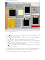
1
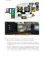
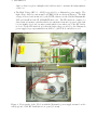
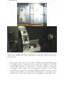
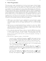
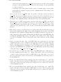
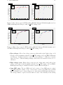
LHCb Collaboration
LHCb 2005-nnn RICH
18th July, 2005
Photo Detector Test Facilities
Production Readiness Review
R. Chamonal, S. Eisenhardt, J. McCarron, F. Muheim
University of Edinburgh
A. Pickford, P. Soler
University of Glasgow
Abstract
This document describes the Photo Detector Test Facilities at the Universities of Edinburgh and Glasgow needed for the Production Readiness Review to be held at Edinburgh
and Glasgow on July 18 and 19, 2005. These test facilities will provide Quality Assurance
for the production of Hybrid Photodiode Detectors (HPD) being built for the LHCb RICH.
1 INTRODUCTION
1
1
Introduction
We have set up two Photo Detector Test Facilities (PDTF) at the Universities of Edinburgh
and Glasgow. These facilities will be used to provide quality assurance (QA) for the LHCb
RICH photo detectors. In total, we expect to measure and verify the specifications of 550
Hybrid Photo Diodes (HPD). At each PDTF site (Edinburgh and Glasgow) we have set-up
two fully equipped test stations. Thus there are four test stations available in total. The
strategy is to use one test station at each site for the mandatory quality assurance tests to
be carried out for provisional acceptance of each HPD as agreed in the contract with the
manufacturer, Delft Electronics Products B.V. (DEP) [1, 2]. The second test station at each
site will be employed for further characterisations to be carried out on a subset of HPDs, for
cross checks of tested HPDs, and for redundancy.
This document is organised as follows: In Section 2 we discuss the organisation and the
logistics of the PDTF project. In Section 3 we give a detailed description of the apparatus.
A description of the DAQ software is given in Section 4. The test programme has been
subdivided into tasks, which are discussed in Section 5. The results from the comparison of
a number of selected tests is shown in Section 6. The document ends with conclusions in
Section 7.
2
Organisation, Plans and Logistics
2.1
Organisation
Within the PDTF team there are several physicists, Ph.D students and technicians. In total
about ten people participate. The FTE fractions of their time allocated to the PDTF project
are given in brackets,
• Physicists: Stephan Eisenhardt (0.8) and Franz Muheim (0.4) at Edinburgh, Andrew
Pickford (0.8) and Paul Soler (0.3) at Glasgow and Reinhardt Chamonal (1.0) during
summer 2005 at Edinburgh.
• Ph.D. students: Judith McCarron (1.0, 0.3 from Oct 2005) at Edinburgh. Two new
students, Robert Lambert (1.0) at Edinburgh and Laurence Carson (1.0) at Glasgow
will start in Oct 2005.
• Technical staff: Andrew Main (0.8) at Edinburgh, Lena Haddad (0.8) and the laboratory manager (0.1) at Glasgow.
In addition, we have access to workshop effort at Edinburgh and Glasgow. It is planned that
additional technical staff step in when Andrew Main and Lena Haddad are not available.
The integrated additional effort is estimated at 0.2 FTE at each site. Most of construction
work, for example the dark boxes, have been carried out at the mechanics and electronics
workshop at Edinburgh.
2 ORGANISATION, PLANS AND LOGISTICS
2
The organisational structure takes into account that the testing is done at two different
geographical sites and that close links are required between the PDTF sites, the manufacturer, CERN and the overall RICH/HPD project. The PDTF project is organised as
follows:
• The QA manager/PDTF project leader (F. Muheim) is responsible for ensuring
– that all HPDs, delivered by DEP, will be tested according to schedule, stored
properly and delivered at CERN to be assembled in the RICH detectors;
– that all essential Quality Assurance data and vendor information are stored in a
central database;
– that there is efficient communication between the PDTF team, the HPD and
RICH project leader;
– and to conduct the overall co-ordination of the test schedule, monitoring and
synchronisation of the test protocols between the two sites.
• The two PDTF site managers (S. Eisenhardt at Edinburgh and A. Pickford at Glasgow)
will be responsible for
– the day-to-day operations at each PDTF site;
– maintaining the test protocols and ensuring that all HPDs are tested accordingly;
– the training of the local students and technical staff;
– keeping close contact with the site manager at the other coast of Scotland and
the QA manager, especially ensuring that problems and bottlenecks are flagged
as soon as they arise.
We currently have a bi-weekly phone meeting with the full HPD team. These meetings are
extremely useful. We also have another weekly meeting within the PDTF team. In addition,
the current work requires daily contacts between the site managers and QA managers.
2.2
Overall Schedule
The overall schedule follows the ammended delivery schedule for the HPDs [3] which is given
in Table 1. Thus 30 HPDs will be delivered each month by the vendor, with one modification.
It has been agreed with DEP that each month two sub-batches of 15 HPDs will be shipped,
one to Edinburgh, one to Glasgow.
The plan is to test one HPD per working day at each PDTF site. One day is the minimum
time required for properly testing an HPD, of which about half a day is required for visual
inspection, mounting the HPD in the dark box, to test for light tightness and carry out the
initial test procedure up to the first ramping of the high voltage up to 20 kV, see Section 5.
The second part of the day is required for carrying out the full test programme.
Testing one HPD per day at each PDTF site allows testing of a full batch of 30 HPDs
within 15 working days or three weeks. In this way we will be testing the HPDs at the same
3 APPARATUS
3
Batch #
0
(9
1
(21
2-3a (30
3b-4 (40
5
(30
...
17
(25
option
option
HPDs)
HPDs)
HPDs)
HPDs)
HPDs)
HPDs)
Delivery
Date
10.01.05
31.07.05
30.09.05
31.10.05
30.11.05
...
30.11.06
TBD
TBD
Table 1: Ammended HPD Production Schedule for a total of 485 HPDs plus options. Batches
5 to 16 consist of 30 HPDs to be delivered at the end of each month.
rate as these are produced. We will also be able to meet the 2 months after delivery deadline
during which CERN is contractually obliged to provisionally accept or reject HPDs. We will
also test 5 HPDs of a sub-batch of 15 HPDs within a week which ensures a reasonably fast
response to possible major production problems.
2.3
Logistics
All HPDs shipped from DEP to Scotland will be under the responsibility of the PDTF
project leader/QA manager. We will set up a simple book-keeping database which will
allow to monitor the status and location of each HPD. The data will be entered via a Webbased interface, and will be stored in a flat-file system. In addition, at each PDTF site there
will be a paper version of the same data with one sheet per HPD.
The communication with DEP and CERN will generally be carried out by the QA manager. During a visit at DEP in March we agreed that we will have standard notifications from
DEP when a shipment has left the company and from us when it has arrived at at PDTF
site. The QA manager will notify CERN when HPDs have been provisionally accepted. The
CERN contact person is Thierry Gys.
Before and after the testing procedures, the HPDs will be stored in the delivery boxes
which give mechanical protection. These boxes will be stored in cabinets under nitrogen flow
in order to minimise the diffusion of helium through the quartz windows.
3
Apparatus
In this section we describe the apparatus. Each PDTF site consists of two fully equipped test
stations. The read-out is based on the CERN HPD DAQ system which was used extensively
in the testing of the pixel chips for the HPD. A schematic of the apparatus is shown in
3 APPARATUS
4
Matsusada
K7−20N
NI field card
SC−2042−RTD
NI cable SH6850
tapped−off pulse
pulser
LED
HV
distr.
cable optional
can be plugged direcly
DAQ PC
PCI Flic
+ Slink
PROM
delay
ADCs
V/ I
monitors
bias pick−up
I
GTL
Data
ZIF socket
SI bias
PT100
LVDS
power
from
DAQs
+5V GND +5V −5V
JTAG
PM3705
COM
(serial
port)
LVDS
HV
conn.
ZIF board
HPD
or
bare chip
LVDS Trig
LVDS Reset
parallel
port
MB board
TTL<−>GTL
serial
FIFO
FPGA
LVDS<−>TTL
40MHz
PC NI PCI
6036E
Control
LVDS<−>TTL
FB board
TAP for MB board
+80V
E3612A
y
TAP for pixel chip
x
stepper motor
controller
Figure 1: Schematics of the PDTF setup.
Figure 2: Photograph of the PDTF setup.
Figure 1. A photograph of the set-up of one testing station is shown in Figure 2.
Each of the four test stations consists of the following major components:
• The Hybrid Photo Diode under test. The Technical Specification of the HPD are
described in the Appendix 1 of the contract [2]. This document will also be Appendix
1 to this report.
• A dark box of dimensions 70 cm x 60 cm x 60 cm. The HPD is mounted to the side
wall of the box. A ZIF socket board mounted to the HPD from the outside of the dark
box provides the connection to the data acquisition. The top and front panel of the
dark box are movable (as in a trunk of a car) in order to provide easy access. In each
3 APPARATUS
5
dark box there is a photo multiplier tube which is used to measure the light tightness
of the box.
• The High Voltage (HV: 0. . . 20 kV) is provided by a Matsusada power supply. The
high voltage divider is custom made at CERN. Both are shown in Figure 8. The high
voltage is steered and monitored by the PDTF software via the National Instruments
PCI card 6036E and the NI SC2042RTD field card. The HV interlock consists of a
daisy chain of four micro-switches which close when the front and top panel of the dark
box are tightly closed and one micro-switch which closes when case of the HV divider
is closed. If the HV interlock is broken the high voltage provided by the Matsusada
power supply drops exponentially from 20 kV to ≤200 V in about half a second.
Figure 3: Photographs of the I/O box with the Matsusada power supply mounted on the
wall (top) and of the HV distribution box opened (bottom).
3 APPARATUS
6
Figure 4: Photographs of the single blue LED feeding light into a multi-mode fibre (top)
and the wheel of LEDs in the dark box with the fibre ending in the centre of the reflection
plane (bottom).
• There are two light sources. One is a single blue LED (wave length 430 nm) located
in the LED trigger box outside the dark box. The light is transmitted to the HPD
via a multimode light fibre. The fibre end is mounted at a distance of about 35 cm
from the HPD quartz window. The divergence of the light is sufficient to illuminate
the full photo cathode surface. The second light source consists of a wheel of nine
blue LEDs inside the dark box. The LEDs illuminate the HPD only indirectly as the
light is scattered diffusely off the back plane of the LED holder, i.e. the same location
where the fibre end is mounted. This produces a flat illumination at the HPD window.
3 APPARATUS
7
The main elements of both light sources are shown in Figure 4. A trigger circuit
produces 10 ns wide current pulses to fire the LEDs. The LEDs are operated at bias
voltages between 0. . . 30 V producing responses of a few photons at the time of the
trigger to sequences of hundreds of photons over several hundred nano-seconds. The
average number of photons per event seen by the HPDs will be set to about two for the
standard tests. The trigger to fire the LEDs is generated from the event trigger sent
to the pixel chip. This trigger is enabled or inhibited in the LED trigger box by lines
which are controlled by the PDTF software for the two light sources separately. The
trigger to fire the LEDs can be programmable delayed via lines on the SC2042RTD
field card in the range of 0. . . 150 ns with respect to the trigger to the pixel chip. A
pin-hole mask can be mounted into the light path. This allows to create a pattern on
the HPD window.
• The read-out electronics for the pixel chip consists of the:
– ZIF board, extension cables and gender adaptor;
– MB (Mike Burns) motherboard and FB (Francois Bal) transmitter board;
The MB board generates all the power supplies and reference signals for the pixel
chip. It also reads the data from the pixel chip and transmits these to the FB
board. The FB board generates the clock and the signals used in the read-out
sequence and transmits these to the MB board. The trigger sent to the LED pulser
is picked up on the FB board by an added wire and routed through an unused
LVDS output. The FB board also receives the pixel chip data and transmits these
down a fast serial link to the FLIC/Slink receiver cards.
– PCI FLIC card and Slink mezzanine receiver card;
The Slink receives and de-serialises the data from the FB board. The FLIC buffers
the data for read-out in the DAQ PC and generates the Event-Readout and Reset
signals initiating the actions of the FB board.
– parallel port JTAG controller;
It provides two channel of slow control to configure the pixel chip and the MB
board.
• Additional infrastructure to control and monitor environmental and HPD parameters
or to provide supplies:
– The voltage to bias the silicon anode of the HPD (0. . . 92 V) is supplied by a
Agilent E3647A power supply which is steered via a GPIB PCI interface.
– The current on the silicon bias line is monitored by a Keithley 6485 pico-Ampere
meter which is read out via the same GPIB PCI interface.
– Pt100 temperature sensors are attached to the ZIF board, to get an estimate of
the chip temperature, and are positioned inside the dark box, to measure the
environmental temperature surrounding the HPD. They are read out via the NI
SC2042RTD field card.
– A low voltage power supply (TTi CPX200) delivers the ±5 V to the FB and MB
board.
4 SOFTWARE DESCRIPTION
8
– A second low voltage power supply (TTi PL320QMT) provides the +24 V supply
for the Matsusada High Voltage power supply, the +5 V for the LED trigger logic
and the precisely regulated 0. . . 30 V for the LED pre-bias.
– A third low voltage power supply (EMS A405) provides the ±12 V for the preamplifier piggy-back circuit on the ZIF board used in the backpulse measurement.
For more details on the MB board, FB board, PCI FLIC card and Slink mezzanine card
see reference [4] which is appended to this report as Appendix 2.
Of the customised electronic units required for the mandatory test programme we have
6 units (4 test stations plus 2 spares) except for the FLIC/Slink receiver cards where only 4
were available. We have 4 units of the commercially available electronics.
Only one station per site, i.e. only two in total, will be equipped with the additional
hardware needed to perform the Backpulse and the Quantum Efficiency measurements as
they only will be carried out on a sub-sample of the HPDs. These tests need the following
additional components:
• The backpulse measurement requires a NIM crate, NIM trigger modules and an amplifier (ORTEC 579). The signal is read out via a PCI based Multi-channel Analyser card
(Trump-PCI-2k) using the proprietary Maestro-32 software to acquire and display the
pulse-hight spectrum.
• The Quantum efficiency measurement is described in [5]. It requires a 90 Sr betaemitting radiation source of activity 100 µCi, a quartz plate of thickness 1 cm and a
holder which places the componets in front of the HPD.
4
Software Description
The data acquisition and data analysis of HPD tests involves a large number of parameters
to be maintained for correct settings and proper sequence. In the Photon Detector Test
Facility (PDTF) software the treatment of the parameters and the sequence of actions and
tests are highly automated. The data acquisition and analysis are integrated as far as possible
to minimise the possibility for human error and to ease the operation when performing the
tests. The software regulates the user interaction to the necessary level. The automation and
integration ensures comparable test results as well as the efficient use of time. In addition
the PDTF software takes care of the proper storage of the measurement results and the
automated logging of the actions, the environmental and monitor parameters.
4.1
Software Packages
Labview 7.1 on Windows XP has been chosen as the main software environment to provide
the graphical surface to the user, to control and monitor the hardware of the test setup, to
take data and to interface to additional analysis tools. For the data acquisition the PDTF
4 SOFTWARE DESCRIPTION
9
software incorporates the Labview based PTS software previously developed at CERN for
the pixel chip testing.
In addition CYGWIN has been installed under Windows XP. This UNIX platform provides the environment to run and maintain shell scrips and compiled analysis code written in
C++. The usage of these tools is integrated into the Labview programmes and transparent
to the user.
Furthermore ROOT has been installed under CYGWIN. The usage of ROOT is not
yet integrated into the operation of Labview. Therefore the legacy analysis tools based on
ROOT have to be preformed by the user interactively in ROOT itself before they are fed
back into the HPD test procedure. ROOT also will be used for further offline analysis and
visualisation of the HPD test data.
The proprietary Maestro-32 software, installed under Windows XP, is used for data
acquisition in the backpulse measurement using the Trump-PCI Multi-Channel-Analyser
card.
Finally a client access to the CERN Oracle database has been installed under Windows
XP. Based on the Java development software it cannot be integrated into the operation of
Labview but also has to be operated interactively by the user after the test series on a HPD
has been completed.
4.2
PDTF Software Outline
The HPD test programme has been divided into a sequence of tasks. Each task is a selfcontained sequence of actions leading to a main result of the HPD tests or a fundamental
state of the test setup.
A main user interface (Labview VI ‘PDTF control.vi’) controls the task flow, governs
the parameter setting global to the HPD testing programme, gathers the environmental
parameters, provides the logging of the actions and the parameters and collects the summary
data of the tests performed by the tasks. No data is overwritten as the names of all produced
files contain a string identifying the creator as well as the date and time of production. The
main user interface runs through a pre-defined task flow but allows for diversions in the
sequence such as repeating or skipping of tasks. Where sensible, the task flow has been
defined to automatically start the next task provided the previous task has reported success.
The definition of the task flow and linkage of tasks can easily be adapted to changing needs
by adjusting the steering parameters in ‘PDTF control globals.vi’. Finally the main user
interface calls the monitors for the hardware parameters outside the data acquisition chain
and continuously checks that they are alive throughout the testing procedure. Figure 5 shows
a screen shot of the PDTF main control and the PDTF monitors in operation together with
a data acquisition tool of the PTS software.
The PDTF software contains four hardware monitors which run independently in parallel
to each other and the rest of the PDTF software. Each of them also can run stand-alone.
The monitors integrate the control and the monitoring of the respective parameters. Their
behaviour can be configured by parameters located in ‘PDTF monitor globals.vi’. The following monitors are provided:
4 SOFTWARE DESCRIPTION
10
Figure 5: Screen shot of the PDTF software in operation: with the main control, the monitors
and a PTS data acquisition tool.
• ‘HV monitor.vi’ controls the 0. . . 20 kV HV power supply to the HPD tube and is
reading back voltage and current.
• ‘BiasV monitor.vi’ controls the 0. . . 92 V bias voltage to the anode inside the HPD and
is reading back the current on this supply line via a pico-Ampere meter.
• ‘LED monitor.vi’ controls the enable state of the two light sources (single blue LED &
light fibre and array of LEDs in dark box) and the 0. . . 150 ns delay of the LED pulse
with respect to the trigger of the data acquisition.
• ‘T monitor.vi’ reads the temperature sensors (on the ZIF board close to the Pixel chip
and inside the dark box).
Several safety features are implemented into the monitors. The maximum ramping rates
for the high voltage and the bias voltage are limited by steering parameters as follows:
• HV: standard rising rate: 50 V/s; standard falling rate: 500 V/s
4 SOFTWARE DESCRIPTION
11
• HV: emergency falling rate: 5000 V/s
• BiasV: standard rising rate: 5 V/s; standard falling rate: 5 V/s
• BiasV: emergency falling rate: 50 V/s
The HV monitor automatically performs an emergency ramp down if limits are passed for
the measured currents on the High Voltage and on the Bias Voltage lines. The HV and the
BiasV monitor automatically switch to standard ramp down if the set and the read back
voltage differ more than a given margin.
The monitors run at different speeds when the focus is on changing of the parameters
(high speed) or on background action (low speed), e.g. when data are acquired. When called
these monitors run in the automatic mode where the input to the monitors is passed in the
background and the front panel only acts as an indicator (exception: the ‘HV emergency
STOP’ can always be used). At any time a monitor can be pulled with a front-panel switch
to ‘local’ (i.e. front-panel) interaction with the user which supersedes any requests passed in
the background.
By default, in the PDTF software the individual tasks are called by the main control.
The location and the names of the files produced by the tasks are then governed by the main
control. The proper function of the tasks may depend on one or more of the monitors being
active. The tasks can also be run in ‘semi-stand-alone’ mode, outside the main control.
In this case, the necessary monitors have to be started stand-alone first. The behaviour
of the tasks can be configured mainly from parameters intrinsic to each task (maintained
in ‘Task xxx globals.vi’ files). The behaviour of the tasks may also depend on parameters
global to the whole testing procedure (maintained in ‘PDTF control globals.vi’). The latter
are also accessed when the tasks are run in semi-stand-alone mode.
The PDTF tasks make use of the PTS software for the control of the data acquisition
chain and data taking. The release ‘PTS 1.4beta’ has been incorporated into the PDTF
Labview package. Some modifications have been applied to add the option of a parallel port
JTAG interface as used in the PDTF setup. All tools of the original PTS package are still
available and can be run stand-alone at any time. The PDTF tasks replace all the interactive
PTS tools with their own user interface tailored to the needs of the HPD testing.
The PDTF tasks may call pre-compiled C++ code for the analysis of the taken data.
The analysis code runs under CYGWIN and can be called from Labview in the background.
The results of the analysis code are read back from output files and standard output and
are checked for errors. The tasks take care of the proper naming and storing of the analysis
results according to the convention maintained by the main control. The tasks log their
own parameters, actions and gathers the results to a file as they proceed. After a task has
finished, this log file is read back and interpreted (by a ‘Task xxx readlog.vi’) to make sure
the gathered data is accessible. From this read back, the selected analysis results are handed
back to the main control for the collection of the summary data.
Further details on the software will be available in PDTF Software User Manual, which
is currently being written by S. Eisenhardt. This document discusses the features of the
software components in detail and provides a reference for the user.
5 TEST PROGRAMME
5
12
Test Programme
The test program consists of individual tests ordered in a logical sequence. In the following
section, the tasks are described in the sequence in which they will be run on the HPDs.
First, the basic functionality of the pixel chip is tested, then the run parameters of the HPD
are determined before the parameter scans can be run in a fully automated way. Thereafter,
further tests are performed which involve again human interaction. Finally the extended tests
are placed at the end of the sequence. They will only be applied to a sub-set of the HPDs and
at a different time and test station than the standard tests for the Quality Assurance. These
tasks are marked with a * in the description below. The specific parameters to be stored
into the database are given. In addition, the major environmental, control and monitored
parameters are recorded and stored to the database. If not mentioned otherwise, data are
taken in the Alice readout mode (256×32 pixels). Some tests are repeated using the LHCb
readout mode (32×32 pixels). The steps of the test programme are:
• JTAG register check verifies the proper communication to the pixel chip by varying
and reading back the register contents. The number of failures in setting the DACs
and in the readings of the readout columns, which should be zero, as well as the final
status.
• DAC linearity scan scans through the full range of settings for a selected set of DACs
of the pixel chip; the voltage profiles are compared by eye to reference data and are
judged by the user for proper function. The number of DACs scanned and the final
status (which should be OK) are then stored.
• IV scan takes the charateristic IV-curve of the anode inside the HPD; the bias voltage
is scanned over the range of 0. . . 90 V and the shape of the curve is judged by the user
to decide whether it is rather diode-like or resistive. The measurement points of the
IV-curve, the bias current at 50 V and 80 V, as well as the judgment on the shape of
the curve are stored.
• Threshold Scans comprises a sequence of six sub-tasks:
– a pre-scan of the overall threshold parameter ‘pre VTH’ with testpulse injection
into the preamplifier of the pixel chip; this three-point scan covers the range of the
fine scan and indicates quickly that the data acqisition is functioning properly;
– a fine scan of ‘pre VTH’ without testpulse injection; this scan gives a profile of the
noise behavour of the assembly and provides the data to choose the final setting
of the overall threshold parameter ‘pre VTH’;
– a procedure to determine and choose the optimum working value of ‘pre VTH’ for
this HPD; this function allows the user to browse through the data of the previous
fine scan and set the value of ‘pre VTH’ which will be used for the remainder of
test programme;
– a pre-scan of the testpulse size ‘test DAC’ with chosen value of ‘pre VTH’; this
three-point scan covers the range of the fine scan and indicates quickly whether
the range of the testpulse size ‘test DAC’ covers well the range of the thresholds;
5 TEST PROGRAMME
13
– a fine scan of the testpulse size ‘test DAC’; this scan gives a profile of the testpulse
response of the individual pixels as well as for the average over the pixels (the
so-called ‘S-curves’);
– an analysis of the data gathered in the scans to determine maps of noisy pixels,
pixels with bad testpulse response and the optimum threshold bit settings of the
individual pixels.
Stored are the chosen ‘pre VTH’ value, the profiles of the fine scans (noise hits vs.
‘pre VTH’ and averaged testpulse response ‘S-curve’), the 50 % point and the slope of
the ‘S-curve’, the maps defining noisy pixels and pixels with no testpulse response and
the map for the optimum settings of the threshold bits of the individual pixels.
• Threshold scan in LHCb mode repeats a fraction of the fine ‘pre VTH’ scan and the
full ‘test DAC’ scan in the LHCb readout mode; the results are compared to those
obtained from the scans taken in Alice readout mode. Stored are the profiles of the
scans, the 50 % point, the slope of the ‘S-curve’ and the indication whether the results
matched.
• High Voltage ramp up and Dark Count rate settling guides the user through a series of
steps slowly ramping up the high voltage while monitoring the response of the HPD
through the data acquisition. During ramp up, the HPD is monitored for response to
dark counts and possible sparks. When resting, the HPD is tested with LED light after
reaching the maximum high voltage. The profile of the settling of the dark counts is
recorded for 30 minutes. Stored is the profile of the dark count rate over the settling
period.
• Strobe scan varies the time delay of the LED light source with respect to the data
acquisition in steps of 5 ns covering the 50 ns wide strobe pulse to the pixel chip. The
profile of the photoelectron response to the LED light is recorded and the optimum
delay for the light pulses is determined. Stored are the profile of the photoelectron
response to the LED light, the optimum delay of the LED pulses and the delay settings
of the pixel chip (‘delay control’ and ‘misc control’).
• Ion feedback rate scan varies the time delay of the LED light source with respect to
the data acquisition in the range of 0. . . 400 ns. The profile of the ion feedback rate
- caused by photoelectrons produced by LED light at an earlier time - is recorded.
Stored are the profile of the ion feedback rate, the maximum rate and the position of
the maximum rate.
• BiasV scan varies the Bias Voltage applied to the anode in the range of 5. . . 80 V. The
profile of the photoelectron response to LED light is recorded. Stored are the profile
of the photoelectron response and the bias voltages needed to achieve 50 % and 90 %
of the maximum response.
• HV scan varies the High Voltage applied to the cathode in the range of 0. . . 20 kV. The
profile of the photoelectron response to LED light is recorded. Stored are the profile
of the photoelectron response and the high voltages needed to achieve 50 % and 90 %
of the maximum response.
5 TEST PROGRAMME
14
• Long LED run collects the photoelectron response to LED light at default settings (in
Alice mode) until each pixel has received about ten hits on average. The LED light
intensity may be increased from the standard two to about five hits per event for this
test. An analysis is run to find the map of dead pixels with no response to light and
a second analysis determines the position, the diameter and the shape of the image of
the photocathode on the anode. The demagnification factor is deduced from this data.
Stored are the average photoelectron response per event, a histogram of the cluster
sizes, the parameters defining the position, size and shape of the photocathode image
and the demagnification factor.
• Dark Count rate collects the photoelectron response without light source (5 M events).
This test takes place about two hours after the initial high voltage ramp up, when
the dark count rate is well settled. Stored are the average photoelectron response per
event and a histogram of the cluster sizes.
• Dark Count rate in LHCb mode repeats the test in LHCb readout mode with lower
statistics (500 k. . . 1 M events). The photoelectron response is compared to that obtained from the measurement taken in Alice readout mode. Stored are the average
photoelectron response per event, a histogram of the cluster sizes and the indication
whether the results matched.
• LED run in LHCb mode repeats the Long LED run in LHCb readout mode. The
photoelectron response is compared to that obtained from the measurement taken
in Alice readout mode. Stored are the average photoelectron response per event, a
histogram of the cluster sizes and the indication whether the results matched.
• Distortion map determines the image quality of the electrostatic focussing of the HPD.
A regular pin hole array with broken symmetry is placed between the LED light source
and the HPD, illuminating only about every fourth pixel in LHCb readout mode in
both directions. The data are taken in Alice readout mode and analysed to check for
the regularity of the recorded pattern and to determine its rotation. Stored are the
rotation angle and the indication on whether the pattern is regular.
• * Backpulse measurement comprises a sequence of four sub-tasks:
– * an initial LED run using the HPD data acquisition to determine the photoelectron response;
– * a measurement of the signal response to LED light on the bias supply line
(backpulse) with the front-end electronics shut down to improve the noise level
on the bias line; the signals are pre-amplified on the ZIF board, amplified in a
NIM based shaping amplifier and measured by a pulse-height sensitive PCI based
ADC;
– * a final LED run using the HPD data acquisition to determine again the photoelectron response;
– * an analysis fitting the ADC spectrum to determine the average number of
photoelectrons per event and a calculation relating the results and calculating
the efficiency for recognising produced photoelectrons on the anode.
6 TEST RESULTS
15
Leakage current
Leakage current
Cern (26.5 C)
2000
1500
Edinburgh (24.5 C)
Glasgow (21.0 C)
Leakage current (nA)
Leakage current (nA)
1500
Cern
Glasgow
1000
1000
500
0
-500
0
10
20
30
40
50
60
Si bias voltage (V)
70
80
90
500
0
-500
0
10
20
30
40
50
60
Si bias voltage (V)
70
80
90
Figure 6: IV curves for HPDs number H428001 (left) and H439004 (right) tested at CERN,
Edinburgh and Glasgow.
Stored are the three average photoelectron responses per event and the photoelectron
recognition efficiency.
• * Quantum Effifiency measurement determines the combined efficiencies of turning a
photon into a photoelectron and recognising it on the anode. A standard light candle, consisting of a 90 Sr beta-emitting radiation source and a quartz plate to produce
Cherenkov photons, is positioned in front of the HPD. The response to the light is
recorded through the HPD data acquisition and compared to the expectation from
the known parameters of the light candle. This measurement integrates over the spectral response of the photo cathode of the HPD. Stored are the average photoelectron
response and the integrated Quantum Efficiency.
As the development of the PDTF software evolves, the grouping of actions into PDTF
tasks might change over time, e.g. the analysis of data becomes automated and part of the
task which acquires the data or related sub-tasks may get integrated into one procedure.
6
Test Results
Two prototype HPDs (HPD number H428001, with pixel chip 4 3 and HPD number H439004,
with pixel chip 3 2) have been tested under similar conditions at CERN, Edinburgh and
Glasgow. In this section, we will show the results from these tests and the comparisons for
the two photodetector test facilities with respect to the CERN testing station.
• IV curves: Figure 6 shows a comparison between the IV curves measured at CERN,
Edinburgh and Glasgow for the two HPDs. Each of the measurements were performed
at different temperatures, so any direct comparison needs to take into account the
temperature difference.
6 TEST RESULTS
16
Bias Scan
1
Bias Scan
Cern
Cern
1
Edinburgh
Edinburgh
Glasgow
0.8
Relative cluster rate
Relative cluster rate
Glasgow
0.6
0.4
0.2
00
0.8
0.6
0.4
0.2
10
20
30
40
50
60
Si bias voltage (V)
70
80
00
90
10
20
30
40
50
60
Si bias voltage (V)
70
80
Figure 7: Bias voltage scans for HPDs number H428001 (left) and H439004 (right) tested at
CERN, Edinburgh and Glasgow, with ‘pre VTH’ setting of 215.
HV Scan
HV Scan
Cern
Edinburgh
1
Cern
Edinburgh
1
Glasgow
Relative cluster rate
Relative cluster rate
Glasgow
0.8
0.6
0.4
0.2
00
0.8
0.6
0.4
0.2
2
4
6
8
10
12
HV (kV)
14
16
18
20
00
2
4
6
8
10
12
HV (kV)
14
16
18
20
22
Figure 8: High voltage scans for HPDs number H428001 (left) and H439004 (right) tested
at CERN, Edinburgh and Glasgow, with ‘pre VTH’ setting of 215.
• Bias voltages: Silicon bias voltage scans were taken with a fixed high voltage of 20
kV and for the discriminator threshold ‘pre VTH’ settings of 215 at CERN, Edinburgh
and Glasgow. Results from these scans are shown in Figure 7. Differences between
curves are due to different timing settings between the test stations and need to be
calibrated.
• High voltage scans: High voltage scans were also taken with a fixed silicon bias
voltage of 80 V and for the discriminator threshold ‘pre VTH’ setting of 215 at CERN,
Edinburgh and Glasgow. Results from these scans are shown in Figure 8.
• Long LED runs: The two HPDs also had a series of long LED runs at a fixed
‘pre VTH’ threshold setting of 215. Screen shots of these long LED runs for HPD
number H428001 can be seen in Figure 9 for data taken at Edinburgh and Glasgow.
The average number of photoelectrons differs because of the intensity in the setting
7 CONCLUSION
17
All events
All events
220
250
250
200
3000
180
200
200
160
2500
140
150
120
150
2000
100
100
80
1500
100
1000
60
50
40
50
500
20
0
0
5
10
15
20
25
events=200000, hits=464769, hits/event=2.32384
30
0
0
0
5
10
15
20
25
30
0
events=2000000, hits=6136943, hits/event=3.06847
Figure 9: Screen shots from long LED runs taken at Edinburgh (left) and Glasgow (right)
of HPD H428001.
of the LED. The rings that can be observed are from multiple reflections in the HPD
quartz window. Both stations identified 2 dead channels for HPD number H428001,
while CERN did not observe any dead channles (the CERN run was taken 6 months
before). For HPD number H439004, Edinburgh measured 2 dead channels and Glasgow
and CERN measured 3 dead channels.
• Dark count rate: The dark count rate was measured for the CERN, Edinburgh and
Glasgow set-ups for both HPDs. These runs were taken at slightly different temperatures but at a fixed ‘pre VTH’ threshold setting of 215. A time-dependent dark-count
rate measured at the Glasgow station for HPD number H428001 can be observed in
Figure 10. The observed number of photoelectrons starts at 0.01 and drops to below
0.0005 photoelectrons (which corresponds to a steady state dark count rate of less than
0.45 kHz/cm2 ) after about 90 minutes.
• Threshold scans: Threshold scans were performed for the CERN, Edinburgh and
Glasgow set-ups and S-curves determining the fraction of hits as a function of ‘pre VTH’
threshold settings were taken. The average threshold was measured to be 1134 e− at
Edinburgh, 1311 e − at Glasgow and 1287 e− at CERN for HPD H428001. The average
variation in threshold setting for all pixels at each of the stations was 97 e− at Edinurgh, 102 e− at Glasgow and 99 e− at CERN. This threshold level meets the LHCb
specifications of less than 2000 e− .
7
Conclusion
The production of 550 Hybrid Photodiode Detectors (HPD) for the LHCb RICH has commenced at our industrial partner Delft Electronics Products B.V. (DEP). The quality assurance of the HPD production will be carried out at two Photodetector Test Facilities (PDTF)
at Edinburgh and Glasgow. Each PDTF site consists of two dedicated test stations (a to-
REFERENCES
18
Dark Counts
0.01
0.008
NPE
0.006
0.004
0.002
00
10
20
30
40
50
60
Time (minutes)
70
80
90
Figure 10: Dark count rate measured as a function of time at the Glasgow station.
tal of four stations) to guarantee the integrity and quality assurance (QA) of each HPD as
agreed in the contract.
This Production Readiness Review (PRR) has described the test facilities at both Edinburgh and Glasgow, the software developed to carry out the tests, the logistics and resources
available for the QA process and results of selected tests performed at CERN, Edinburgh
and Glasgow. The four stations are ready to receive production HPDs. Final calibration
procedures between stations are being carried out to enable consistency between the stations
and to guarantee the certification process for the HPDs manufactured.
References
[1] “Supply of Hybrid Photon Detectors for the LHCb Rich Counters”, Contract No.
F549/PH/LHCb. CERN (2005).
[2] “Technical specification for the supply of pixel Hybrid Photon Detectors for the LHCb
ring Imaging Cherenkov system”, F549/PH/LHCb Appendix 1, (2005) CERN EDMS
ID 498198 v1.
[3] T. Gys, “HPD project status”, LHCb RICH meeting (LHCb week 7 June) CERN,
http://agenda.cern.ch/fullAgenda.php?ida=a053217.
[4] K. Wyllie, “Pixel HPD Test System Hardware Description, v1.0”, CERN (2004),
http://kwyllie.home.cern.ch/kwyllie/LHCBPIX1.htm
[5] B. Cikoski, “Cerenkov Candle and Analysis of Multianode Photomultiplier”, MsC
thesis, University of Edinburgh (2003)
http://www.ph.ed.ac.uk/particle/Exp/group/INTERNAL/internal.htm.