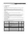
1
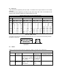
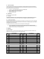
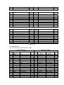
To our customers,
Old Company Name in Catalogs and Other Documents
On April 1st, 2010, NEC Electronics Corporation merged with Renesas Technology
Corporation, and Renesas Electronics Corporation took over all the business of both
companies. Therefore, although the old company name remains in this document, it is a valid
Renesas Electronics document. We appreciate your understanding.
Renesas Electronics website: http://www.renesas.com
April 1st, 2010
Renesas Electronics Corporation
Issued by: Renesas Electronics Corporation (http://www.renesas.com)
Send any inquiries to http://www.renesas.com/inquiry.
Notice
1.
2.
3.
4.
5.
6.
7.
All information included in this document is current as of the date this document is issued. Such information, however, is
subject to change without any prior notice. Before purchasing or using any Renesas Electronics products listed herein, please
confirm the latest product information with a Renesas Electronics sales office. Also, please pay regular and careful attention to
additional and different information to be disclosed by Renesas Electronics such as that disclosed through our website.
Renesas Electronics does not assume any liability for infringement of patents, copyrights, or other intellectual property rights
of third parties by or arising from the use of Renesas Electronics products or technical information described in this document.
No license, express, implied or otherwise, is granted hereby under any patents, copyrights or other intellectual property rights
of Renesas Electronics or others.
You should not alter, modify, copy, or otherwise misappropriate any Renesas Electronics product, whether in whole or in part.
Descriptions of circuits, software and other related information in this document are provided only to illustrate the operation of
semiconductor products and application examples. You are fully responsible for the incorporation of these circuits, software,
and information in the design of your equipment. Renesas Electronics assumes no responsibility for any losses incurred by
you or third parties arising from the use of these circuits, software, or information.
When exporting the products or technology described in this document, you should comply with the applicable export control
laws and regulations and follow the procedures required by such laws and regulations. You should not use Renesas
Electronics products or the technology described in this document for any purpose relating to military applications or use by
the military, including but not limited to the development of weapons of mass destruction. Renesas Electronics products and
technology may not be used for or incorporated into any products or systems whose manufacture, use, or sale is prohibited
under any applicable domestic or foreign laws or regulations.
Renesas Electronics has used reasonable care in preparing the information included in this document, but Renesas Electronics
does not warrant that such information is error free. Renesas Electronics assumes no liability whatsoever for any damages
incurred by you resulting from errors in or omissions from the information included herein.
Renesas Electronics products are classified according to the following three quality grades: “Standard”, “High Quality”, and
“Specific”. The recommended applications for each Renesas Electronics product depends on the product’s quality grade, as
indicated below. You must check the quality grade of each Renesas Electronics product before using it in a particular
application. You may not use any Renesas Electronics product for any application categorized as “Specific” without the prior
written consent of Renesas Electronics. Further, you may not use any Renesas Electronics product for any application for
which it is not intended without the prior written consent of Renesas Electronics. Renesas Electronics shall not be in any way
liable for any damages or losses incurred by you or third parties arising from the use of any Renesas Electronics product for an
application categorized as “Specific” or for which the product is not intended where you have failed to obtain the prior written
consent of Renesas Electronics. The quality grade of each Renesas Electronics product is “Standard” unless otherwise
expressly specified in a Renesas Electronics data sheets or data books, etc.
“Standard”:
8.
9.
10.
11.
12.
Computers; office equipment; communications equipment; test and measurement equipment; audio and visual
equipment; home electronic appliances; machine tools; personal electronic equipment; and industrial robots.
“High Quality”: Transportation equipment (automobiles, trains, ships, etc.); traffic control systems; anti-disaster systems; anticrime systems; safety equipment; and medical equipment not specifically designed for life support.
“Specific”:
Aircraft; aerospace equipment; submersible repeaters; nuclear reactor control systems; medical equipment or
systems for life support (e.g. artificial life support devices or systems), surgical implantations, or healthcare
intervention (e.g. excision, etc.), and any other applications or purposes that pose a direct threat to human life.
You should use the Renesas Electronics products described in this document within the range specified by Renesas Electronics,
especially with respect to the maximum rating, operating supply voltage range, movement power voltage range, heat radiation
characteristics, installation and other product characteristics. Renesas Electronics shall have no liability for malfunctions or
damages arising out of the use of Renesas Electronics products beyond such specified ranges.
Although Renesas Electronics endeavors to improve the quality and reliability of its products, semiconductor products have
specific characteristics such as the occurrence of failure at a certain rate and malfunctions under certain use conditions. Further,
Renesas Electronics products are not subject to radiation resistance design. Please be sure to implement safety measures to
guard them against the possibility of physical injury, and injury or damage caused by fire in the event of the failure of a
Renesas Electronics product, such as safety design for hardware and software including but not limited to redundancy, fire
control and malfunction prevention, appropriate treatment for aging degradation or any other appropriate measures. Because
the evaluation of microcomputer software alone is very difficult, please evaluate the safety of the final products or system
manufactured by you.
Please contact a Renesas Electronics sales office for details as to environmental matters such as the environmental
compatibility of each Renesas Electronics product. Please use Renesas Electronics products in compliance with all applicable
laws and regulations that regulate the inclusion or use of controlled substances, including without limitation, the EU RoHS
Directive. Renesas Electronics assumes no liability for damages or losses occurring as a result of your noncompliance with
applicable laws and regulations.
This document may not be reproduced or duplicated, in any form, in whole or in part, without prior written consent of Renesas
Electronics.
Please contact a Renesas Electronics sales office if you have any questions regarding the information contained in this
document or Renesas Electronics products, or if you have any other inquiries.
(Note 1) “Renesas Electronics” as used in this document means Renesas Electronics Corporation and also includes its majorityowned subsidiaries.
(Note 2) “Renesas Electronics product(s)” means any product developed or manufactured by or for Renesas Electronics.
To all our customers
Regarding the change of names mentioned in the document, such as Hitachi
Electric and Hitachi XX, to Renesas Technology Corp.
The semiconductor operations of Mitsubishi Electric and Hitachi were transferred to Renesas
Technology Corporation on April 1st 2003. These operations include microcomputer, logic, analog
and discrete devices, and memory chips other than DRAMs (flash memory, SRAMs etc.)
Accordingly, although Hitachi, Hitachi, Ltd., Hitachi Semiconductors, and other Hitachi brand
names are mentioned in the document, these names have in fact all been changed to Renesas
Technology Corp. Thank you for your understanding. Except for our corporate trademark, logo and
corporate statement, no changes whatsoever have been made to the contents of the document, and
these changes do not constitute any alteration to the contents of the document itself.
Renesas Technology Home Page: http://www.renesas.com
Renesas Technology Corp.
Customer Support Dept.
April 1, 2003
3DK38124
USER MANUAL
FOR H8/38124 ON-CHIP FLASH
MICROCONTROLLER
Warning
Check the silkscreen around the power jack (J9) for the minimum and maximum voltage input levels for this 3DK.
Always use a centre positive supply for this board.
DO NOT USE AN E6000 POWER SUPPLY with this 3DK
Preface
Cautions
1.
This document may be, wholly or partially, subject to change without notice.
2.
All rights reserved. No one is permitted to reproduce or duplicate, in any form, a part or this
entire document without Renesas Technology Europe Limited's written permission.
Trademarks
General
All brand or product names used in this manual are trademarks or registered trademarks of their
respective companies or organisations.
Document Information
Product Code:
D005610_11
Version:
1
Date:
22/11/2004
Copyright © Renesas Technology Europe Ltd. 2004. All rights reserved.
Website:
http://www.eu.renesas.com/
TABLE OF CONTENTS
TABLE OF CONTENTS .......................................................................................................................................................3
1.
POWER REQUIREMENTS ..........................................................................................................................................4
2.
POWER – UP BEHAVIOUR ........................................................................................................................................4
3.
PURPOSE ...............................................................................................................................................................4
4.
BOARD LAYOUT ......................................................................................................................................................4
5.
BLOCK DIAGRAM ....................................................................................................................................................6
6.
USER CIRCUITRY ....................................................................................................................................................6
6.1. SWITCHES...........................................................................................................................................................6
6.2. LEDS ....................................................................................................................................................................6
6.3. SERIAL PORT ......................................................................................................................................................7
6.4. JUMPERS.............................................................................................................................................................7
7.
OSCILLATOR SOURCES ...........................................................................................................................................8
8.
MODES ...................................................................................................................................................................8
8.1. BOOT MODE........................................................................................................................................................8
8.2. USER MODE ........................................................................................................................................................8
9.
PROGRAMMING METHODS .......................................................................................................................................8
9.1. PORT PROGRAMMING.......................................................................................................................................9
9.2. FDM HEADER ......................................................................................................................................................9
9.3. E7 HEADER..........................................................................................................................................................9
9.4. OFF-BOARD PROGRAMMING............................................................................................................................9
10. HEADERS ...............................................................................................................................................................9
10.1. MICON HEADERS................................................................................................................................................9
10.2. GENERIC HEADERS .........................................................................................................................................10
11. CODE DEVELOPMENT ............................................................................................................................................11
11.1. OVERVIEW ........................................................................................................................................................11
11.2. MODE SUPPORT...............................................................................................................................................11
11.3. BREAKPOINT SUPPORT ..................................................................................................................................11
11.4. CODE LOCATED IN RAM..................................................................................................................................11
11.5. HMON CODE SIZE.............................................................................................................................................11
11.6. MEMORY MAP...................................................................................................................................................12
11.7. BAUD RATE SETTING.......................................................................................................................................13
11.8. INTERRUPT USAGE..........................................................................................................................................13
11.9. ADDITIONAL INFORMATION ............................................................................................................................13
1. POWER REQUIREMENTS
All 3DK boards are centre positive with a 2.5mm barrel power jack.
The diode, D1 provides reverse polarity protection.
A 9V, centre positive supply is suitable for use with this board.
Warning
Check the silkscreen around the power jack (J9) for the minimum and maximum voltage input levels for this 3DK.
The 3DK is neither under nor over voltage protected.
Always use a centre positive supply for this board.
DO NOT USE AN E6000 POWER SUPPLY with this 3DK
2. POWER – UP BEHAVIOUR
The 3DK board has code pre-programmed into the Renesas microcontroller. On powering up the board,
the red user LEDs will start to flash. Switches 2 and 3 as well as the potentiometer can be used to modify
the LED flashing pattern.
3. PURPOSE
This 3DK board is an evaluation tool for Renesas microcontrollers.
Features include:
a. Renesas Microcontroller Programming
b. User Code Debugging
c. User Circuitry such as Switches, LEDs and potentiometer(s)
d. User or Base Board Connectivity
The 3DK board contains all the circuitry required for microcontroller operation.
4. BOARD LAYOUT
The following diagram shows the component layout top layer component of the board.
Note: The diagram below is for illustrative purposes and does not accurately reflect the 3DK detailed in this
manual.
RES
J3
DEBUG
U1
OFF
USER
SWITCHES
ON
MICON
HEADER
J2
MICON
HEADER
J3
MCU_SEL
FLASH
HEADER
J4
19-WAY
GENERIC
HEADER J5
MCU
SELECT
SWITCH
SW3
SERIAL
PORT
CLED8
CLED7
Renesas
Microcontroller
J8
CLED6
SW2
CLED5
CLED4
BOOTJ7
USER
LEDS
J12
CLED3
J2
POWER
JACK
SW1/BOOT
J5
J6
CLED2
J9
CLED1
BOOT LED
J1
BOOT
MICON
SINGLE TURN
HEADER POTENTIOMETER
J4
MICON
HEADER
J1
DEBUG
HEADER
20-WAY
GENERIC
HEADER
J6
The following diagram shows the component layout bottom layer component of the board. Note: The diagram
below is for illustrative purposes and does not accurately reflect the 3DK detailed in this manual.
RS232
Transceiver
IC
BOOT LATCH
U2
C 2004 Renesas Technology Europe LTD.
HC74 dual
D-type logic
U5
Crystal / Oscillator /
Resonator Components
/ Footprints
U6
PCB Component Placing Top
PCB Component Placing Bottom
Regulator
IC
5. BLOCK DIAGRAM
Diagram 5.1 is representative of the 3DK components and their connectivity.
Power Jack & Regulator IC
Generic Headers
Microcontroller
Boot mode pins
Flash/Boot Header
Micon Headers
RESET pin
Boot Circuitry
RESn
D-type latch
BOOT & BOOTn signals
IRQ pin
IRQ pin
IRQ pin
Serial Connector
Debug Header
SW2
RES
SW3
BOOT
SWITCHES
LEDs
3 Red LEDS
1 Green
LED
6. USER CIRCUITRY
6.1. SWITCHES
There are four switches located on the 3DK. These are:
Switch
Function
Microcontroller
SW1/BOOT
This switch is used in conjunction with the RES switch to place the
device in BOOT mode.
SW2
This switch is connected via a 0R link to an IRQ line capable of
waking up the microcontroller device from sleep mode.
SW3
This switch is connected via a 0R link to another IRQ line capable of
waking up the microcontroller device from sleep mode.
RES
This switch when pressed resets the 3DK microcontroller.
NB. Refer to schematic for detailed connectivity information.
IRQ0
(Port 4 –3)
IRQ4
(Port 1 –4)
IRQ3
(Port 1 – 7)
RESn
6.2. LEDS
There are four LEDs on the 3DK board. The green BOOT LED indicates the device is in boot mode when lit. The
three red LEDs are connected to an IO port and will light when their corresponding port pin is set low.
Table 6-1, below, shows the LED pin references and their corresponding microcontroller port pin connections.
LED Reference (As shown
on silkscreen)
CLED1
CLED2
CLED3
Microcontroller Port Pin function
Port 9 – 0
Port 9 – 1
Port 9 – 2
Table 6-1:LED Port
Microcontroller Pin Number
54
55
56
6.3. SERIAL PORT
The microcontroller programming serial port (SCI3) is connected to the D–type connector J8 via an RS232
transceiver.
The serial baud rates supported by this 3DK are shown below. Note: these values are calculated from the
frequency value of the main oscillating source fitted by default on this 3DK.
Baud Rate Register Settings for Serial Communication Rates
Values are calculated for 9.8304MHz clock
SMR
Setting:
Comm.
Baud
0
BRR
setting
Actual
Rate
1
ERR
(%)
110 Invalid
Invalid
Invalid
300 Invalid
Invalid
Invalid
BRR
setting
2
Actual
Rate
Invalid
Invalid
ERR
(%)
BRR
setting
Invalid
3
Actual
Rate
ERR
(%)
BRR
setting
Actual
Rate
ERR
(%)
86
110.3
0.31
21
109
-0.83
127
300
0.00
31
300
0.00
7
300
0.00
0.00
1200
127
1200
0.00
31
1200
0.00
7
1200
0.00
1
1200
2400
63
2400
0.00
15
2400
0.00
3
2400
0.00
0
2400
4800
31
4800
0.00
7
4800
0.00
1
4800
0.00 Invalid
Invalid
Invalid
9600
15
9600
0.00
3
9600
0.00
0
9600
0.00 Invalid
Invalid
Invalid
19200
7
19200
0.00
1
19200
0.00 Invalid
Invalid
Invalid
Invalid
Invalid
Invalid
38400
3
38400
0.00
0
38400
0.00 Invalid
Invalid
Invalid
Invalid
Invalid
Invalid
57600
2
51200
-11.11 Invalid
Invalid
Invalid
Invalid
Invalid
Invalid
Invalid
Invalid
Invalid
0 153600
33.33 Invalid
Invalid
Invalid
Invalid
Invalid
Invalid
Invalid
Invalid
Invalid
115200
0.00
Table 6-2 : BRR Settings
This serial port may be used as a debugging communication port or as a normal serial communication port when
the device is in user mode.
5
4
9
3
8
2
7
1
6
Female serial
connector showing
pin numbering
Power Jack
6.4. JUMPERS
Table 6-3 below describes the function of the 2-Pin jumpers contained on this 3DK board.
2-Pin Jumper Settings
Reference
Jumper
Function
Fitted
Alternative
(Removed)
J10
RX Disable
PRXD from the RS232
device to U1 is enabled.
This enables serial port
communication.
Disabled. This
allows the FDM
to program the
microcontroller
Jumper pins fitted
J11
UVCC power
Measurement
Bypasses R11, a 1206 0R
resistor,
for
current
measurement
R11 must be
fitted to power
UVCC
Footprint only
Table 6-4: 2-Pin jumpers
Footprint for jumper
only/Jumper pins fitted
7. OSCILLATOR SOURCES
A crystal resonator is fitted on the 3DK and used to supply the main clock input to the Renesas microcontroller.
Table 7-1 details the oscillators that are fitted on this 3DK:
Component
Details
Crystal
Subclock
Yes
9.8304MHz
38400
Yes
32.768 kHz
N/A
Table 7-1: Oscillators / Resonators
Warning: When replacing the default oscillator with that of another frequency, the FDT programming kernels
supplied will need rewriting. The supplied HMON debugging monitor will not function. The user is responsible for
code written to support operating speeds other than the default. See the HMON user manual for details of making
the appropriate modifications in the code to accommodate different operating frequencies.
8. MODES
The 3DK supports User mode and Boot mode. User mode may be used to run user code, while Boot mode may
be used to program the Renesas microcontroller with program code and to debug code.
To enter boot mode, the mode pins are held in their boot states while reset is pressed and released. The BOOT
LED will be illuminated to indicate that the microcontroller is in boot mode.
8.1. BOOT MODE
The boot mode settings for this 3DK are shown in Table 8-1 below:
TEST
0
0
NMI
1
0
P36
X
1
LSI State after Reset End
User Mode
Boot Mode
Table 8-1: Mode pin settings
8.2. USER MODE
For the device to enter User Mode, reset must be held active while the microcontroller mode pins are held in
states specified for User Mode operation. 100K pull up and pull down resistors are used to set the pin states
during reset.
The H8/38124 supports only normal mode, which has a 64-kbyte address space.
9. PROGRAMMING METHODS
The Flash ROM on the microcontroller can be programmed when the device is in Boot mode. Once in boot mode,
the bootloader program stored in the microcontroller executes and attempts a connection with a host (for example,
a PC). The host, on establishing a connection with the microcontroller, may then transmit program data to the
microcontroller via the appropriate programming port.
Table 9-1 below shows the programming port for this Renesas Microcontroller and its associated pins
Programming Port Table – Programming port pins and their 3DK signal names
SCI3
TXD, PIN 71
RXD_1, PIN 70
3DK Signal Name
PTXD
PRXD
Table 9-1: Serial Port Boot Channel
9.1. BOOT PROGRAMMING
The microcontroller must enter boot mode for programming, and the programming port must be connected to a
host for program download. To execute the boot transition, and allow programs to download to the microcontroller,
the user must perform the following procedure:
1.
2.
3.
4.
Connect a 1:1 serial cable between the host PC and the 3DK board
Depress the BOOT switch and keep this held down
Depress the RESET switch once, and release
Release the BOOT switch
9.2. FDM HEADER
This 3DK does not support the FDM.
9.3. E7 HEADER
The Renesas E7 Debugger is a tool for debugging Renesas microcontrollers, available separately from Renesas.
The E7 utilises SCI4 on the microcontroller. The device may be debugged and programmed using the E7.
9.4. OFF-BOARD PROGRAMMING
All 3DKs are capable of programming an alternative microcontroller on a secondary board. The user is responsible
for providing this second board containing the alternative microcontroller, its supporting circuitry and an FDM or
FoUSB header for the microcontroller.
To program the alternative microcontroller, the user should perform the following steps
•
•
Connect a cable between the 3DK programming header and that located on the secondary board.
Slide switch MCU_SEL to the off-board programming position (OFF). This holds the microcontroller on
the 3DK in reset, preventing it from being programmed.
10. HEADERS
10.1. MICON HEADERS
Table 10-1 to Table 10-4 shows the micon headers and their corresponding microcontroller connections. The
header pins connect directly to the micon pin unless otherwise stated.
J1
Pin
1
3
5
7
9
11
13
15
17
19
Circuit Net Name
CON_AVCC (AVCC via a 0R link)
CON_X2 (X2 via a 0R link)
CON_OSC2 (OSC2 via a 0R link)
U1 pin
number
1
3
5
7
9
11
13
15
17
19
J1 pin
number
2
4
6
8
10
12
14
16
18
20
Circuit Net Name
CON_X1 (X1 via a 0R link)
CON_OSC1 (OSC2 via a 0R link)
U1 pin
number
2
4
6
8
10
12
14
16
18
20
Table 10-1: J1
J2
Pin
1
3
5
7
9
11
13
15
Circuit Net Name
U1 pin
number
21
23
25
27
29
31
33
35
J2 pin
number
2
4
6
8
10
12
14
16
Circuit Net Name
U1 pin
number
22
24
26
28
30
32
34
36
17
19
37
39
18
20
38
40
Table 10-2: J2
J3
Pin
1
3
5
7
9
11
13
15
17
19
Circuit Net Name
CON_PIN57 (PIN57 via a 0R link)
U1 pin
number
41
43
45
47
49
51
53
55
57
59
J3 pin
number
2
4
6
8
10
12
14
16
18
20
Circuit Net Name
U1 pin
number
42
44
46
48
50
52
54
56
58
60
Circuit Net Name
U1 pin
number
62
64
66
68
70
72
74
16
78
80
Table 10-3: J3
J4
Pin
Circuit Net Name
1
3
5
7
9
11
13
15
17
19
U1 pin
number
61
63
65
67
69
71
73
75
77
79
J4 pin
number
2
4
6
8
10
12
14
16
18
20
Table 10-4: J4
10.2. GENERIC HEADERS
Table 10-5 below shows the generic header connections
19 way generic Header
Pin
Number
1
2
3
4
5
6
7
8
9
10
11
12
13
14
15
16
17
18
19
Generic
Header Name
Supply
Xin
Vcc
Vss
Vcc
Vss
AVcc
AVss
Vref
AN0
AN1
AN2
AN3
DAC0
DAC1
SCL
SDA
CTX
CRX
3DK Signal Name
Supply
CON_OSC1
VCC1
GROUND
VCC2
GROUND
AVCC
AVSS
VREF
PIN77
PIN78
PIN79
PIN80
Not Connected
Not Connected
Not Connected
Not Connected
Not Connected
Not Connected
20 way generic Header
Micon
Pin
N/A
10*
N/A
N/A
N/A
N/A
52
53
N/A
77
78
79
79
80
NC
NC
NC
NC
NC
Pin
Number
1
2
3
4
5
6
7
8
9
10
11
12
13
14
15
16
17
18
19
Generic Header
Name
IOPORT_TXD
IOPORT_RXD
IOPORT_T1
IOPORT_T2
IOPORT_T3
IOPORT_T4
IOPORT_U
IOPORT_V
IOPORT_W
IOPORT_0
IOPORT_1
IOPORT_2
IOPORT_3
IOPORT_4
IOPORT_5
IOPORT_6
IOPORT_7
/Reset
/NMI
3DK Signal
Name
IOPORT_TXD
IOPORT_RXD
IOPORT_T1
IOPORT_T2
IOPORT_T3
IOPORT_T4
Not Connected
Not Connected
Not Connected
IOPORT_0
IOPORT_1
IOPORT_2
Not Connected
Not Connected
Not Connected
Not Connected
Not Connected
RESn
IOPORT_INT
Micon
Pin
N/A
N/A
63
62
67
68
NC
NC
NC
54
55
56
NC
NC
NC
NC
NC
12
N/A
20
VSS
GROUND
Table 10-5: Generic Headers
* Connected via a DNF 0R Link, refer to schematic for further details.
11. CODE DEVELOPMENT
11.1. OVERVIEW
Note: For all code debugging using Renesas software tools, the 3DK board must be connected to a PC serial port
via a serial cable.
The HMON embedded monitor code is modified for each specific 3DK Renesas Microcontroller. HMON enables
HEW to establish a serial connection to the 3DK microcontroller, and control code execution on the
microcontroller. The HMON embedded monitor code must be compiled with user software and downloaded to the
3DK, allowing the users’ code to be debugged within HEW. The board must be operated in BOOT mode during
debugging.
11.2. MODE SUPPORT
The HMON library is built to support Normal Mode only. The Device supports only Normal Mode.
11.3. BREAKPOINT SUPPORT
The monitor has an address break controller with one break channel, therefore one breakpoint can be located in
ROM. Code located in RAM may have multiple breakpoints limited only by the size of the On-Chip RAM.
Due to a limitation of the internal address break controller, a breakpoint set in ROM will execute the instruction at
the breakpoint and stop on the subsequent op-code. The break controller only functions in BOOT mode.
11.4. CODE LOCATED IN RAM
Double clicking in the breakpoint column in the code sets the breakpoint. Breakpoints will remain unless they are
double clicked to remove them.
11.5. HMON CODE SIZE
HMON is built along with the debug code. Certain elements of the HMON code must remain at a fixed location in
memory. The following table details the HMON components and their size and location in memory. For more
information, refer to the map file when building code.
Section
Description
Start Location
Size
(H’bytes)
RESET_VECTOR
HMON Reset Vector (Vector 0)
Required for Startup of HMON
TRAPA Instruction Vector (Vector 8)
Required by HMON to create Breakpoints in RAM
HMON Break Controller (Vector 10)
Required by HMON to create Breakpoints in ROM
HMON Serial Port Vectors (Vector 18)
Used by HMON when EDK is configured to connect to the
default serial port.
HMON Code
HMON Constant Data
HMON Uninitialised data
H’ 0000 0000
2
H’ 0000 0010
2
H’ 0000 0014
2
H’ 0000 0024
2
H’ 0000 27f2
H’ 0000 4684
H’ 0000 f780
1e92
e1
1fd
H’ 0000 0400
1a8
H’ 0000 2000
5d1
H’ 0000 0100
2
TRAP_VECTORS
HW_BREAK_VECTORS
SCI_VECTORS
PHMON
CHMON
BHMON
FDTInit
FDTUserModeMicroKernel
CUser_Vectors
FDT Init Kernel.
This is at a fixed location and must not be moved. Should
the kernel need to be moved it must be re-compiled.
FDT User Mode Kernel.
This is at a fixed location and must not be moved. Should
the kernel need to be moved it must be re-compiled.
Pointer used by HMON to point to the start of user code.
N/A
11.6. MEMORY MAP
The memory map shown in this section visually describes the locations of program code sections related
to HMON, the FDT kernels and the supporting code within the ROM/RAM memory areas of the
microcontroller.
H'0000
H'0100
Vectors
RESET Vector
H'0000
H'0001
TRAP Vector
H'0010
H'0011
HW Break Vector
H'0014
H'0015
SCI Vectors
H'0024
H'0025
CUser_Vectors
H'0400
FDTInit
H'05A7
H'2000
H'25D0
H'27F2
On-Chip FLASH
ROM
FDTUserM ode
M icroKernel
On-Chip FLASH
ROM
PHM ON
CHM ON
H'4764
On-Chip FLASH
ROM
H'7FFF
H'F020
Internal I/O
REGISTERS
H'F02B
H'F740
LCD RAM 16 Bytes
H'F74F
H'F780
H'F9E8
BHM ON
1-kbyte work area
for reprogram ing
FLASH
H'FB7F
H'FB80
1k User RAM
H'FE80
H'FF7F
H'FF80
H'FFFF
Stack
Internal I/O
REGISTERS
11.7. BAUD RATE SETTING
HMON is initially set to connect at 38400 Baud. The value set in the baud rate register for the microcontroller must
be altered if the user wishes to change either the serial communication baud rate of the serial port or the operating
frequency of the microcontroller. This value is held in the HMONserialconfiguser.c file, as SCI_CFG_BRR (see the
Serial Port section for baud rate register setting values). The project must be re-built and the resulting code
downloaded to the microcontroller once the BRR value is changed. Please refer to the HMON User Manual for
further information.
11.8. INTERRUPT USAGE
Because HMON uses the serial port, interrupts using a higher priority cannot be used while debugging. In practice
this means that only the ADC interrupt can be used reliably during debugging.
11.9. ADDITIONAL INFORMATION
For details on how to use High-performance Embedded Workshop (HEW), with HMON, refer to the HEW manual
available on the CD or from the web site.
For information about the H8/38024-H8/38124 series microcontrollers refer to the H8/38024 Series Hardware
Manual
For information about the H8/38124 assembly language, refer to the H8 Series Programming Manual
Further information available for this product can be found on the Renesas web site at:
http://www.eu.renesas.com/tools
General information on Renesas Microcontrollers can be found at the following URLs.
Global:
http://www.renesas.com/