1
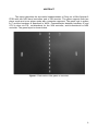
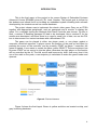
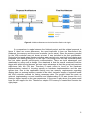
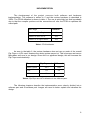
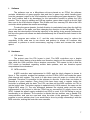
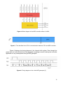
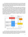
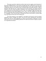
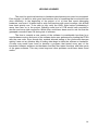
Final Report
"Pong"
EDA385 - Design of Embedded Systems
[Advanced Course]
Group:
Henrik Ljunger
[email protected]
Sebastian Mellström
[email protected]
Renato Casas-Cordero
[email protected]
Supervisor:
Flavius Gruian
[email protected]
2014-10-26
ABSTRACT
This report describes the successful implementation of Pong on a Xilinx Spartan 6
FPGA with two NES hand controllers and a VGA monitor. The game supports both two
player mode and a one player mode with a computer opponent. The game logic is written
in C and the hardware is described in VHDL. Communication between hardware IP and
CPU is done via FSL, uni-directional for the VGA controller, and bi-directional for NES
controller. The game layout is shown below.
Figure 1: Final version of the game on a monitor.
2
TABLE OF CONTENTS
Abstract . . . . . . . . . . . . . . . . . . . . . . . . . . . . . . . . . . . . . . . . . . . . . . . . . . . . . . . . . . . 2
Introduction . . . . . . . . . . . . . . . . . . . . . . . . . . . . . . . . . . . . . . . . . . . . . . . . . . . . . . . . 4
Implementation . . . . . . . . . . . . . . . . . . . . . . . . . . . . . . . . . . . . . . . . . . . . . . . . . . . . . 6
Software . . . . . . . . . . . . . . . . . . . . . . . . . . . . . . . . . . . . . . . . . . . . . . . . . . . . . . 7
Hardware . . . . . . . . . . . . . . . . . . . . . . . . . . . . . . . . . . . . . . . . . . . . . . . . . . . . . . 7
FSL buses . . . . . . . . . . . . . . . . . . . . . . . . . . . . . . . . . . . . . . . . . . . . . . . . . 7
NES controller . . . . . . . . . . . . . . . . . . . . . . . . . . . . . . . . . . . . . . . . . . . . . 7
VGA controller . . . . . . . . . . . . . . . . . . . . . . . . . . . . . . . . . . . . . . . . . . . . . 9
Problems and Solutions
. . . . . . . . . . . . . . . . . . . . . . . . . . . . . . . . . . . . . . . . . . . . . 13
Lessons learned . . . . . . . . . . . . . . . . . . . . . . . . . . . . . . . . . . . . . . . . . . . . . . . . . . . . . 14
Conclusions . . . . . . . . . . . . . . . . . . . . . . . . . . . . . . . . . . . . . . . . . . . . . . . . . . . . . . . . 15
Contributions . . . . . . . . . . . . . . . . . . . . . . . . . . . . . . . . . . . . . . . . . . . . . . . . . . . . . . . 16
User Manual . . . . . . . . . . . . . . . . . . . . . . . . . . . . . . . . . . . . . . . . . . . . . . . . . . . . . . . . 17
References . . . . . . . . . . . . . . . . . . . . . . . . . . . . . . . . . . . . . . . . . . . . . . . . . . . . . . . . . 18
3
INTRODUCTION
This is the final report of the project in the course Design of Embedded Systems
Advanced Course (EDA385) given at LTH, Lund, Sweden. The project goal is chosen by
the students and should focus on building an embedded system including both software
developed by the students as well as custom hardware
The project chosen was to implement the classic video game Pong on an FPGA
together with appropriate peripherals, such as gamepads and a monitor to display the
game. For a nostalgic feeling the Nintendo 8-bit Hand Controller was chosen. For this to
work, a custom IP handling gamepad I/O had to be developed. Also a custom IP for the
monitor was developed, and since there is no need to send a lot of data, we use the FSL
bus to interconnect our custom hardware with a Microblaze CPU.
The game can be played in either two player mode, or one player against a
computer controlled opponent. A player moves the position of the pad up and down by
pressing the arrow on the controller, and by pressing START on player 1 controller, the
game is started. If one wants to restart the game, press SELECT. The second player has
to press START on her control to join the game, otherwise the right player on the monitor
will be controlled by the AI. The ball moves and bounces by itself, and every time it hits
one of the walls or the pads, a new trajectory is calculated to make the game harder and
dynamic.
Figure 2: Final architecture.
Figure 2 shows the final layout. Boxes in yellow and blue are located on-chip, and
gray is existing hardware.
4
Figure 3: Initial architecture to the left and the final to the right.
If a comparison is made between the finished project and the original proposal in
figure 3, there are some differences, the most important is how we interconnect the
hardware, the memory and the sound controller (as an extra). Since the memory needed
for the VGA controller was not known at start, it was included in the first specification.
During the first week when literature studies were carried out a new high level design was
proposed, the resulting design is on the right. This design does not use a shared system
bus but rather specific point-to-point communication. There are both advantages and
drawbacks by using such a design. One drawback is that the overall overhead could be
bigger with point-to-point busses, but one major advantage is that the group had previous
experience with the FSL bus. Therefore it made sense to focus on the hardware
implementation instead of focusing equally on hardware implementation and the new
system bus. Due to the application having very low memory requirements regarding
display data, no external memory needed to be used. Instead a couple of registers inside
the VGA controller sufficed for saving necessary data. The project listed two parts as
optional, implementing a sound controller and implementing AI. AI was chosen due to it
having a higher impact on the user experience. If one were to play alone, the game would
have no real support for this. Therefore a simple CPU enemy is created that controls the
right player.
5
IMPLEMENTATION
The development of the project concerns both software and hardware
implementation. The software is written in C and the custom hardware is described in
VHDL. The FPGA utilization is shown in table 1. The use is quite high, but that is probably
due to that the compiler portions out the connections all over the FPGA to optimize the
critical path.
Slice Logic
Utilization
Number of Slice Register
8%
Number of Slice LUTs
24%
Number of occupied Slices
39%
Table 1: FPGA utilization.
As seen in the table 2, the custom hardware does not use so much of the overall
Flip Flops or LUTs used. However the whole system uses a lot. This is because we have a
Microblaze soft-core in our design. Since this is a pipelined design, this will increase the
Flip Flops used drastically.
IP
Flip Flops used
LUTs used
Whole System
2412
2884
VGA
122
347
NES
50
68
Table 2: Flip Flops and LUTs utilization for the different parts.
The following chapters describe the implementation more closely, divided into a
software part and a hardware part. Images are used to better explain and visualize the
design.
6
I.
Software
The software runs on a Microblaze soft-core placed on an FPGA, the software
contains initialization of game-specific data and then a game loop which handles input
from the gamepad, output to the VGA controller, score-keeping and game dynamics. Three
low level routines had to be developed for the instructions needed to update the VGA
monitor. This is done by shifting and OR-ing together game data to build up the bit field
later seen in the VGA monitor chapter. This is then sent via a one-way FSL bus to the VGA
controller which updates the monitor accordingly.
To make the game dynamic, the ball direction is recalculated every time the ball hits
one of the walls or the pads, and thus changing the direction of the ball slightly. The AI
player was first developed to follow the trajectory of the ball by doing smooth movements,
but since the game now allows two balls simultaneously the AI tracks the ball closest to the
score line.
The program was written in C, and the main technique used to reduce the
complexity of the code was to use structs and pointers to structs. All functions take
references to pointers to avoid unnecessary copying of data and increase the overall
speed.
II. Hardware
A. FSL buses:
The project uses five FSL buses in total. The NES controllers use a duplex
connection to avoid having a large buffer and therefore simply poll the controller of button
data, while the VGA controller uses a simplex connection. The reason for this is that the
CPU needs no feedback regarding monitor data updates, and can therefore spend
computational time elsewhere.
B. NES controller:
A NES controller was implemented in VHDL and the block diagram is shown in
figure 4. The controller strobes the hardware via the FPGA’s GPIO and reads the game
pads internal shift register. The result is 8 bits where every bit maps to a button on the
gamepad. Therefore it is possible for the software to discover if more than one button is
pressed at a given instance. Every time 8 bits have been read, a register inside the
controller is updated with the data. The CPU can then poll the NES controller via FSL to
get the button data. The button-register is updated every 1/60th second, the same as the
original NES setup [1]. The only difference between the original setup and the setup
implemented in this project is that the FPGA has no convenient 5V supply close to the
GPIO. Instead the power supply available from GPIO is used, 3.3V. Still timing is met so
functionality is not affected. The controller is divided into two entities, one to handle FSL
communication, and one two read and store the state of the gamepad. This makes it
possible to use an arbitrary bus if one would like to do so by simply connecting it with the
NES controller, making the controller more versatile.
7
Figure 4: Block diagram of the NES controller written in VHDL.
Figure 5: The data field in the FSL in communication between CPU and NES controller.
Figure 6 displays the timing diagram of the internal shift register. Even though the
game does not need all data from the gamepad everything is saved, making the controller
applicable for any development using a NES gamepad.
Figure 6: Timing diagram of the of the NES gamepad [1].
8
To avoid parasitic effects, all data-, latch- and the pulse pins are terminated to
ground via a 4.5 kΩ resistor. The idea from the beginning was to order a female connector
online and solder on wires which would have provided a stable connection to the FPGA.
Unfortunately the connector was not easy to find, so instead thin wires are used to
interconnect breadboard and controller and then jumper cables between breadboard and
GPIO on the FPGA. The resulting connection is shown in figure 7.
Figure 7: The connection between the gamepads and the FPGA.
C. VGA controller:
The second custom made hardware part that was implemented in VHDL was a VGA
controller that generates the image displayed on the screen. The controller outputs a
stream of frames at the rate of 60 Hz at a resolution of 640x480 pixels. Depending on the
frame rate and resolution the VGA interface uses different clock speeds and timing
information. For the resolution of 640x480 pixels at 60 Hz the clock frequency should be
25 MHz with the timing information in table 3.
Horizontal timing
Pixels
Vertical timing
Pixels
Visible area
640
Visible area
480
Front porch
16
Front porch
10
Sync pulse
96
Sync pulse
2
Back porch
48
Back porch
33
Whole line
800
whole frame
525
Tableta 3: Timing information for the VGA with the resolution 640x480 and refresh rate 60 Hz[2].
9
The horizontal sync pulse tells the display that the end of a row has been reached
and that it should jump to the next and in the same way the vertical sync pulse indicates
when it’s time to start a new frame. Before and after each sync pulse there is a time slot
called front porch respectively back porch that is outside of the display area, these exists
because the VGA interface originally was developed for CRT screens where the electron
beam needed time to change rows etc[3].
A block diagram over the VGA controller is shown in figure 8. The controller uses
the 100 MHz clock from the FPGA board but the chosen resolution needs to increment the
pixel at a frequency of only 25 MHz. The block called pixel_clk simply set the signal
pixel_en high for one clock cycle every fourth clock cycle. The block timing_ctrl handles
the timing of the VGA interface, it uses counters to keep track of the current pixel position
in both horizontal and vertical direction. The signal pixel_en is used together with the clock
to increment the horizontal pixel position and when the end of a row is reached the vertical
pixel position is incremented. The signal pixel_en is not used as clock signal since doing
this would introduce logic in the clock path which in most cases is undesirable. All timing
information such as the front, back porches and the sync pulses widths are hard coded as
constants in the timing_ctrl block, it is therefore not possible to change the resolution
without changing the hardware.
Figure 8: Block diagram over the implemented VGA controller.
The VGA controller communicates with the CPU through a FSL where the VGA
controller is in slave mode and the CPU in master mode, it is one way communication
where the VGA controller only reads data. The FSL has a FIFO depth of one to save area
and has a 32- bit wide data field allowing multiple information parts to be sent at once. The
CPU uses three simple instructions, shown in figure 9, to send data.
10
Figure 9: The instructions used for communication between CPU and VGA controller.
The block bus_ctrl is responsible for decoding these instructions and save the data
in the appropriate registers. The two least significant bits are used to determine the
instruction which gives a total of four instructions as shown in table 4.
SEL
Operation
00
No Operation
01
Pad Data
10
Ball Data
11
Score Data
Table 4: The instructions with their corresponding SEL value.
The controller stores the Y- positions of the pads in a 10- bit wide register to allow
the pads to move across the whole display and it is the current position that is sent in the
instruction. The movement of the pads is done completely in the software that is
responsible for updating the positions. The pad instruction also contains fields for changing
the heights of the pads. The height is set by shifting the value from the instruction to the
left by two bits i.e. multiplying by four.
The ball instruction contains the X and Y- positions both 10- bit wide and an ID bit that
indicates which of the two balls the data belongs to. The score instruction includes both
the players’ current score and they are 8- bit wide.
11
The image_gen block reads the position data from the registers and determines if
the current display position on the screen is on the pads, balls, middle lines or on the score
segments. If that is the case it sets all of the RGB outputs to ones which is white otherwise
it keeps the output to zero which is black. Information about the pads X-position, width of
the pads, balls and lines etc. is hard coded into the VGA controller. The image_gen block
decides if the color should be white by checking if the current display position on the Xaxis is bigger than the start position on the X- axis of for example a pad and smaller than
the end position and the same applies for the Y- axis. If the four conditions are true then
the color should be white and this procedure is the same for all the objects on the screen.
For readability of the code the parts concerning the score was moved to a block called
seg_disp which functions just as the image_gen.
The VGA controller is very specific to our project and cannot be used in another
application without changing the VHDL code. But the parts regarding the VGA timing
should work with any other application as long as the resolution is 640x480 at 60 Hz.
Otherwise the way of communicating with the CPU and how and what to display is specific
to our applications demand.
12
PROBLEMS AND SOLUTIONS
Throughout the project we had a problem with unreliable connection between the
NES controller and the FPGA- board. This was because we used simple cords to connect
the controller and a simple solution would have been to get a female connector. This
problem was not due to the software or any of the hardware on the board and was outside
the project scope but solving it would have been convenient to us. The connection is
shown in figure 10.
Figure 10: The connection of a gamepad.
Another irritating problem is a really thin line being visible on the screen where there
should not be anything displayed. This probably arises from the fact that the output in the
VGA controller is combinatorial. This problem only occurred on some runs of the system
and sometimes it did not occur. A simple solution could be to stabilize the output by placing
a register between the combinatorial part and the output.
There was also a problem with trying to add a moving gradient color background to
the game. Adding color had the unwanted effect to also change the balls and pads from
white to another color like yellow or pink depending on the background color. This could
also be because of the combinatorial output. The solution was to keep to black and white
display and instead focusing on adding another ball to the game. The possible solution
was discovered after the demonstration and it has therefore not been implemented and
tested.
The group had problems with how to make the AI- player behave realistically so that
it was possible to win against it. This was already hard when the game only included one
ball but the introduction of two balls made it very hard. There were also problems with the
AI getting stuck at the top of the display and moving past the screen borders. This was due
to some logical errors in the software and when they were solved there was not enough
time to implement a realistic AI so in the end the decision was made to make the AI- player
perfect with the consequence that it is impossible to win against it.
13
LESSONS LEARNED
The need for good test benches in hardware development can never be overstated.
Even though it is hard to write good test benches this is something that we should have
done differently. In the beginning of the project a lot of time was spent debugging
hardware, and even if it takes time to write test benches with good coverage, this should
have been priority one. To be able to fully verify the VHDL code before synthesizing it
saves time later on in the project. Building some kind of PCB would have provided a
sturdier and more rigid connection. Which then could have been used to rule out that the
gamepad connection was OK during test of software.
The time to compile a new version of the software is considerable less than for a
new hardware version and most of the software tests were performed by loading the FPGA
with the new code. Even though this method allowed testing of the performed changes
quickly it was not an effective way of finding other bugs in either the software or hardware.
A better way would have been to develop a program that tested every part of the
interaction between software and hardware and that also tested functions and other parts
of the game software. This way some bugs and other problems could have been found
earlier.
14
CONCLUSIONS
Since the connection between the breadboard and NES controller consists of thin
wires with bare ends pushed into the socket, the connection is unstable from time to time.
To avoid these, two female sockets could have been ordered and even two small PCBs
could have been created, but since the simple solution worked most of the time, this was
decided to be good enough. To change this into a more long-term solution would definitely
be an improvement.
The game software is good structured and easy to understand, but there could
probably be improvements that are not done. One improvement that would need small
adjustment to the hardware is adding support for one additional ball. This would not
increase the complexity of neither software nor hardware by much, but changes would
have to be made.
As always when working with FPGA’s one is astonished by how much that is
possible to do with the right tools. Creating an embedded system that creates real value,
like a recreational game, is necessarily not that hard.
15
CONTRIBUTIONS
The report has been divided evenly where each person wrote about his part, and
the other chapters are written together. It is hard to do any time estimates but we believe
that we spend equally much time on the project and on the report. The group has mostly
worked in alternating pairs during testing, and doing pure developing privately.
% Henrik:
Building system
VGA controller
Testing
Final presentation
% Sebastian:
NES controller + Hardware required
Software (minor)
Testing
Final presentation
% Renato:
Proposal presentation
Software (major)
Testing
16
USER MANUAL
This user manual focuses on general information. The C code, VHDL code and
everything needed to run this project can be downloaded from the course page.
Board instructions:
I.
Build the system in XPS.
II.
Export & launch SDK.
III. Connect monitor and gamepads according to picture, D3 and D4 are not used.
Connect latch1 to JA2, pulse1 to JA3, data1 to JA1
Connect latch2 to JB2, pulse2 to JB3, data2 to JB1
Figure 11: Pin layout of the NES gamepad.
IV. Program the FPGA via Adept (make sure that you chose the correct file).
V.
Start playing, have fun!
Playing instructions:
% By default, player 1 (left player) start playing against the “AI player”. The second
player has to press START on her control to join the game, otherwise the right
player on the monitor will be controlled by the AI.
% Player 1 special keys:
○ SELECT: Reset the whole game. (Positions/Score/Players)
○ START: Start the game after each point.
% Both players move UP/DOWN with respective arrows on the NES pad.
17
REFERENCES
% [1] http://www.mit.edu/~tarvizo/nes-controller.html 2014-10-26
% [2] http://tinyvga.com/vga-timing/640x480@60Hz 2014-10-24
% [3] https://courses.engr.illinois.edu/ece412/MP_files/mp3/vga_timing.pdf 2014-10-24
18