1
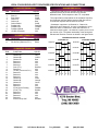
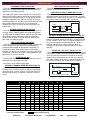
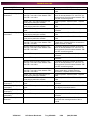
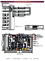
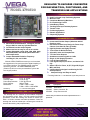
MODEL 2790500 RESOLVER TO ENCODER CONVERTER FOR MACHINE TOOL, POSITIONING, AND TRANSFER LINE APPLICATIONS *** APPLICATIONS *** Ideal For Closed Loop Positioning Systems Machine Tools Coordinate Measuring Machines PLC Positioning Control Index/Rotary Tables Tracking/Telescope/Telemetry Systems Transfer Lines Positioning Systems Robotic Applications Dispensing Systems *** ADVANCED FEATURES *** RESOLVER TO DIGITAL INTERFACE Works with Harowe/Danaher, Tamagawa, Kerfott, Singer, AMCI or most any Synchro/Resolver Incremental encoder output signals Makes resolvers as easy to use as an encoder Jumper Selectable counts 1000, 1024, 2000, 2048, 4000, 4096, 8000, and 8192 A-quad-B with Index and complements Jumper Selectable Excitation Frequency VEGA 2779501 for Inductosyn Scale Applications including 2.5, 5.0, and 10 kHz With the VEGA 2790500 converter you can have both the ruggedness of an resolver and the digital simplicity of an encoder interface. The 2790500 can be used with almost any resolver. The INDEX/MARKER pulse (Channel Z) will occur once per transducer cycle at the zero degree position. 2790500 2.5, SPECIFICATIONS Excitation: 5, or 10 kHz Excitation: 2.5, 5, or 10 kHz Resolver Input: 0.8 to 18 vpp Power Requirements: 5 vDC @ 250 mA Drive Capacity: 200 mA Peak Mechanical: 5.250 x 2.825 x 1.000 5.400 x 3.500 x 1.850 w/DIN Accuracy: +/- 3 arc minutes typical CONVERTER ACCURACY AND TRACKING RATE The tracking rate is a function of the excitation frequency and quadrature counts. With a 2.5 kHz excitation and 4000 quadrature counts the tracking rate would be 9,600 rpm. With a 10.0 kHz excitation and 4000 quadrature counts the tracking rate would be 38,400 rpm. Reducing the counts will increase the tracking rate proportionately. Incremental Encoder Output (*Absolute within 1 Resolver cycle) Non-Phase Locked Loop Design for Faster Loop Closure (Less than 50 uSec @ 10 kHz) High Resolution and Highly Accurate Tuned Filter for Noise Immunity A-Quad-B, Index and Complements TTL/Line Driver Outputs Quadrature encoder signals to 4 mHz Single +5 vDC Supply Operation Loss of Phase Detection Fault Signal Output (Line Driver, and Active PullUp) Status LED’s for Power, A, B, Z, Signal HI, Signal MID, and Fault Configurable Fault signal conditioning for FailSafe operations Compact Design and Easy to Install * Tracking limited to +/- 0.25 Resolver cycle with power off PRICING AND DELIVERY Model 2790500 2790DIN 2790CK1 2790CK2 Description Resolver to Digital DIN Rail Kit Solder Connector Kit Crimp Connector Kit Please ask your MACCON sales representative for a quotation. 2790500_Rev. E VEGA CNC 1270 Souter Boulevard Troy, MI 48083 USA (248) 585-3600 VEGA 2790500 RESOLVER TO ENCODER SPECIFICATIONS AND CONNECTIONS P1 RESOLVER CONNECTOR PIN# 1 2 3 4 5 6 7 8 9 10 FUNCTION Sine HI Sine LO Sine Shield Cosine HI Cosine LO Cosine Shield Feedback HI Feedback LO Feedback Shield +5 vDC (*External) COLOR Red Black SHLD Yellow Blue SHLD Red/Wht Yel/Wht SHLD N/A P2 POWER CONNECTOR PIN# *1 *2 FUNCTION +5 vDC (*Same as P1-10) DC Ground (*Same as P1-1) COLOR Red Black P3 ENCODER CONNECTOR PIN# 1 2 3 4 5 6 7 8 9 10 11 12 13 14 15 16 17 18 19 20 21 22 23 24 25 FUNCTION DC Ground (*Same as P2-2) Channel A+ Channel B+ Channel Z+ Reserved Reserved Reserved Fault (TTL) Reserved +5 vDC (*Same as P2-1) Reserved Reserved Reserved Channel AChannel BChannel ZReserved Reserved !Fault (Active Pull-Up) !Fault (TTL) Reserved Reserved Reserved Reserved Active Pull-Up vDC VEGA CNC COLOR Black Grey Yellow Blue N/A N/A N/A Blu/Red N/A Red N/A N/A N/A Violet Orange Green N/A N/A Red/Blk Blu/Blk N/A N/A N/A N/A Blu/Wht 1270 Souter Boulevard QUADRATURE OUTPUT The VEGA 2790 series of converter boards use RS-422-A differential drivers to provide 40 mA into a 100 ohm differential load. These outputs are also TTL compatible. The output latency is dependent on the excitation frequency. At 2.5 kHz the response will be less than 200 uSec and at 10.0 kHz the response will be less than 50 uSec. Quadrature is provided via Channel A+, Channel A-, Channel B+ and Channel B-. A count is considered to occur whenever there is a transition in either the Channel A or Channel B output signals. The Channel Z (Index) occurs once per resolver cycle. The phase relationship of the two signals indicates the direction of motion as shown in the figure below. QUADRATURE OUTPUT FORMAT COUNTING UP COUNTING DOWN CHAN A+ CHAN A+ CHAN A- CHAN A- CHAN B+ CHAN B+ CHAN B- CHAN B- CHAN Z+ CHAN Z+ CHAN Z- CHAN Z0 1 Troy, MI 48083 2 3 4 USA 0 (248) 585-3600 1 2 3 4 JUMPER SETTINGS FREQUENCY SELECTION (B1-B2) The 2790 series of converters provide selectable excitation frequencies via SWB1 jumpers B1 and B2. Most resolver applications are tuned to 2.5 kHZ. FAULT MODE OUTPUT SELECTION The 2790 converter board provides several methods of interface for fail safe fault detection. DIFFERENTIAL FAULT SIGNAL SET-UP (J4) Installing a jumper on J4 pins 1-2 enables the RS-422-A differential drivers and provide up to 40 mA into a 100 ohm differential load. These outputs are also TTL compatible and are located on pins 8 and 20 of the P3 connector. The 2790 also provides jumper selection of the active filter network for the return signal to provide the maximum noise immunity at the selected frequency. For the typical resolver application operating at 2.5 kHZ both J10 and J11 jumpers should be installed. For excitation frequencies above 2.5 kHZ both jumpers should be removed. For low level signal condition at 2.5 kHZ J10 can be removed to achieve a x4 internal gain. DECIMAL/BINARY SELECTION (B3) The 2790 converter card provides both decimal and binary counting modes. Installing SWB1 jumper B3 selects binary counting mode to provide selection between 256, 512, 1024, and 2048 line counts. Removing jumper B3 selects the decimal counting mode to provide selection between 250, 500, 1000, and 2000 line counts. FAULT 8 FAULT 20 SHLD TTL OR LINE DRIVER INTERFACE TRI-STATE A-QUAD-B FAULT SIGNAL SET-UP (J4) Install a jumper on J4 pins 2-3. The 2790 board will TriState the A-Quad-B signals as well as the Z Channel during a Fault condition. The +/- Fault TTL signals located on P3 pins 8 and 20 are also Tri-Stated and are NOT a valid interface with this set-up. This interface will allow an immediate Fault sense by equipment with loss of signal detection. LINE COUNT SELECTION (B4-B5) The 2790 converter board provides 8 jumper selectable line counts. Binary counts are selected by installing SWB1 jumper B3 and installing the appropriate combination of jumpers B4 and B5. Most systems using encoder style feedback are set to the x4 quadrature counting mode so that the effective quadrature counts are 4 times greater than the physical line count of the encoder. ACTIVE PULL-UP FAULT SIGNAL SET-UP The active pull-up interface is a fail-safe design so that in a loss of power condition the 2790 will still drop the fault signal on Pin 19 of the P3 connector. Pin 19 will be the source voltage with no fault present and can drive up to 600 mA. The source voltage for the Pull-up must be provided on Pin 25 of the P3 connector and can range from 5-40 vDC. RESERVED (B6-B9) On the 2790 converter board Jumpers B6-B9 are reserved and should have all jumpers removed See Figure 1.0 for SWB1 Jumper Chart. CHANNEL Z NORMAL/INVERTED SELECTION (J2) The 2790 converter board provides jumper selectable inversion of the Z Channel (Index) for systems requiring an active low signal. Jumper J2 pins 2-3 select the channel Z Normal mode and pins 1-2 select the Channel Z Inverted mode. FUNCTION 2.5 kHZ 5.0 kHZ 10.0 kHZ Reserved Decimal Count Binary Count 250/256 Lines 500/512 Lines 1000/1024 Lines 2000/2048 Lines Default Reserved Reserved Reserved Reserved B1 0 1 0 1 1 Indicates installed jumper VEGA CNC B2 0 0 1 1 B3 25 +5 to +40 VDC GND 19 FAULT CR F1 F1 - 1 AMP ACTIVE PULL-UP INTERFACE B4 B5 0 1 0 1 0 0 1 1 B6 B7 B8 B9 Quadrature Counts 0 1 1000 Decimal/1024 Binary 2000 Decimal/4048 Binary 4000 Decimal/4096 Binary 8000 Decimal/8192 Binary 0 1 0 0 0 1 1 1 - Figure 1.0 Indicates default setting 1270 Souter Boulevard Troy, MI 48083 USA (248) 585-3600 RESOLVER SET-UP PROCEDURE 1) Install the 2790 board as described in the application drawing 2790500 2) Select the fault signal conditioning method by setting the J4 jumper as described in the JUMPER SETTINGS section and the jumper table (Fig. 1.0) based on the application requirements. 3) Select the Z Channel inverted option by setting J2 to short pins 1 and 2. The DEFAULT is non-inverting and having pins 2 and 3 shorted on J2. 4) Select the excitation frequency by JB1-2 of SWB1 (see jumper table Fig. 1.0). 2.5 kHZ is the DEFAULT setting with both jumpers removed. 5) Select the passive filter setting by J11 for the corresponding frequency setting. The DEFAULT setting is for a board set to 2.5 kHZ and J11 is installed. 6) Select the counting style of Binary or Decimal by JB3 of SWB1 (see jumper table Fig. 1.0). Decimal is the DEFAULT setting with the jumper removed. 7) Select the line count per revolution by setting JB4-5 of SWB1 (see jumper table Fig. 1.0). 1000 lines per revolution (4000 quadrature counts per revolution) is the DEFAULT setting with JB4 removed and JB5 installed. 9) J10 selects in the input course gain range and allows for interface to a broad range of resolver transformation ratios. Installing a jumper on pins 1 and 2 sets the gain to 0.25 (gain of ¼). Installing a jumper on pins 2 and 3 sets the gain to 1.0 and removing the jumpers completely sets the gain to 4.0. 10) Turn the gain potentiometer fully counter-clockwise. Then turn the gain potentiometer clock-wise until the MID LED comes on. The signal return on “ST1” test point should now be 3.8 volts peak to peak. Phase the position loop if necessary by reversing the Sine HI and Sine LO wires to reverse the count direction. At this point the basic set-up is complete and the position loop can now be closed. Set the position loop gain of the servo system and then continue to Step 11. 11) After the position loop has been closed the phase balance of the 2790 board can be adjusted. To adjust the phase balance of the 2790 board, observe the excitation return on the “ST1” test point. Adjust the oscilloscope to 100 mvDC per division and offset the signal so that just the peak of the signal is visible. Jog the axis at 30% of its feedrate. If the phase is unbalanced the peak of the sine wave will bounce and become blurred. Adjust the balance pot (BAL) on the 2790 to achieve 20 mvDC or less bounce. 8) Jumpers JB6-8 are reserved on the 2790500 and should be removed. LED STATUS INDICATORS CHA = Channel A State Indicator CHB = Channel B State Indicator CHZ = Channel Z (Index/Marker) Indicator PWR = Power Status Indicator FLT = Loss of Signal Indicator MID = Return Signal Proper Indicator HSG = High Signal Indicator VEGA CNC 1270 Souter Boulevard TEST POINTS GND PA+ PAPB+ PB- = Analog Ground = Sine HI (3.6 vDC Peak to Peak) = Sine LO (3.6 vDC Peak to Peak) = Cosine HI (3.6 vDC Peak to Peak) = Cosine LO (3.6 vDC Peak to Peak) SIG = Signal Return (0.8-18.0 vDC Peak to Peak) ST1 = Stage 1 Signal (3.8 vDC Peak to Peak) SCL = Tracking Clock Troy, MI 48083 USA (248) 585-3600 TROUBLE SHOOTING SYMPTOM CHECKS SOLUTION No Power LED Check +5 vDC Fault LED (Low Signal) Continuous Remove power and ohm between “PA+“ and “PA-“ note value. Ohm between “PB+” and “PB-“ note value. Fault LED (Low Signal) Intermittent Remove power and ohm between “PA+“ and “PA-“ note value. Ohm between “PB+” and “PB-“ note value. Check “PA+” and “PA-“test point for 3.6 volts peak to peak sine excitation Check “PB+” and “PB-“test point for 3.6 volts peak to peak sine excitation Check “ST1” test point for 3.8 volts peak to peak +5 vDC Present Board Failure – Replace board If resistance values are less than 30.0 ohms – Check for shorts between “PA-“ and “PA+” as well as ground. Check for shorts between “PB-“ and “PB+” as well as ground. Signal not present Board Failure – Replace board Signal not present Board Failure – Replace board Repeat Step 9-10 of the Resolver Set-Up Procedure Signal not present Board Failure – Replace board Signal not present Board Failure – Replace board If resistance values differ by more than 3 ohms of each other Check Resolver connections – Replace resolver or cables If resistance values are less than 30.0 ohms – Check for shorts between “PA-“ and “PA+” as well as ground. Check for shorts between “PB-“ and “PB+” as well as ground. Repeat step 11 of the Resolver Set-Up Procedure Repeat step 11 of the Resolver Set-Up Procedure If resistance values are less than 30.0 ohms – Check for shorts between “PA-“ and “PA+” as well as ground. Check for shorts between “PB-“ and “PB+” as well as ground. If resistance values are differ by more than 3 ohms of each other Check Resolver connections – Replace resolver or cables Signal not present Board Failure – Replace board Signal not present Board Failure – Replace board Repeat Step 9-10 of the Resolver Set-Up Procedure Check “ST1” test point for 3.8 volts peak to peak Signal Proper Follow procedures described in the Fault LED (Low Signal) Intermittent section No Problem… Life is Good Check “ST1” test point for bounce Repeat step 11 of the Resolver Set-Up Procedure None Swapping the Sine HI with the Sine LO wires will reverse the counting direction of the Aquad-B Check “PA+” and “PB+“test point for 3.6 volts peak to peak sine excitation Check “PA-” and “PB-“test point for 3.6 volts peak to peak sine excitation Check “ST1” test point for 3.8 volts peak to peak Check “PA+” and “PB+“test point for 3.6 volts peak to peak sine excitation Check “PA-” and “PB-“test point for 3.6 volts peak to peak sine excitation Remove power and ohm between “PA+“ and “PA-“ note value. Ohm between “PB+” and “PB-“ not value. Remove power and ohm between “PA+“ and “PA-“ note value. Ohm between “PB+” and “PB-“ note value. Check “ST1” test point for bounce Cyclic Error Check “ST1” test point for bounce Remove power and ohm between “PA+“ and “PA-“ note value. Ohm between “PB+” and “PB-“ note value. HSG LED (High Signal) Continuous HSG LED (High Signal) Intermittent MID LED (Signal Midpoint) Continuous MID LED (Signal Midpoint) Intermittent Feedback Polarity is Reversed VEGA CNC 1270 Souter Boulevard Troy, MI 48083 USA (248) 585-3600 MECHANICAL AND APPLICATION DRAWINGS HAROWE/DANAHER, TAMAGAWA, KERFOTT, SINGER, AMCI RESOLVER AND HOLLOW SHAFT RESOLVERS *** POWER CONNECTIONS *** USE P2 SCREW TERMINALS OR P3 CONTACTS FOR POWER ENTRY VEGA 2790500 RESOLVER TO ENCODER P2 P1 +5 VDC 1 1 SIN HI BLUE DC GND 2 2 SIN LO YELLOW 3 SHIELD *NOTE P3 +5 VDC 10 4 COS HI RED DC GND 9 5 COS LO BLACK 6 SHIELD 75 FEET MAX CHAN A+ 2 CHAN A- 14 7 FDBK HI YEL/WHT 8 FDBK LO RED/WHT 9 SHIELD SHLD 10 CHAN B+ 3 CHAN B- 15 300 FEET MAX RECOMENDED CABLE: BELDON 8103 OR EQUIVALENT SHLD CHAN Z+ 4 CHAN Z- 16 SHLD FAULT 8 FAULT 20 SHLD +5 to +40 VDC GND CR 25 FAULT SCALE VEGA 1270 SOUTER *NOTE: THE DC RETURN OF THE +5 VDC SHOULD BE BONDED TO EARTH GROUND DRAWN CHECKED TROY, MI 48083 ENGINEER DATE THIS DOCUME NT CO NTAINS PRO PRIE TA RY INFORM ATIO N AND SUCH INFO RMATIO N M AY NO T BE DIS CLO SE D TO O THERS FOR ANY PURPO SE OR USED FO R M ANUFACTURING PUPO SE S W ITHO UT WRITTEN PE RMIS IO N FROM INNO VATIVE SUPPO RT SERVICE S INC. 19 W.O.# SHEET NO. N/A CAST CAST WLH 08-25-12 2790 1 OF 1 NAME: 2790500 Resolver Application Interface SIZE A INCH DIMENSIONS VEGA CNC 1270 Souter Boulevard Troy, MI 48083 USA (248) 585-3600 DRAWING NUMBER 2790500 CHANGE ELECTRICAL POWER REQUIREMENTS The 2790500 converter requires +5 vDC supply @ 250 mAmp for operation. The supplied power should have less than 50 mVolts of noise and drift. Recommended Power Supplys (If Required) Mean Well MDR-20-5 (+5 vDC @ 3 Amps) Mean Well MDR-40-5 (+5 vDC @ 6 Amps) CABLE SPECIFICATIONS The 2790 series of converters provide stable and precise sine and cosine excitations. These signals and the return signal are analog and proper routing and shielding techniques should be observed. Shielded twisted pair cables should be used for all interface signals. Recommended Cable Shielded Twisted Pair with Drain Wire Belden #8103 or equivalent ACCESSORIES and SUPPORT Connector Kits and Mounting Options KIT #2790CK1 Includes: (1) DB-25 Male Solder Cup Connector (1) DB-25 Plastic Hood and Hardware KIT #2790CK2 Includes: (1) DB-25 Male Crimp Style Connector (25) Gold Male Crimp Pins (1) DB-25 Plastic Hood and Hardware * Use Molex Crimper HTR2445A or general purpose crimper HT202A (Jameco PN 99443) KIT #2790DIN Includes: (1) DIN Rail Mount for 2790 boards REPAIR AND TECHNICAL SUPPORT Monday-Friday 8:00am to 6:00pm Eastern VEGA CNC 1270 Souter Boulevard Troy, MI 48083 USA (248) 585-3600