1
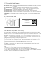
M
DBM 04
User's Manual
GB-4517 Rev.9 - Oct/01
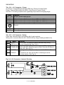
DBM 04 - USER'S MANUAL
Rev. Date
Description
Sept/96
Initial Release
0
25/Nov/96 Add CE-marking according to LVD; correct Tab.3.6 (IT
1
protection); add reference to conductive coating
20/Feb/97 Correct J1 connector pinout; add figure with single phase
2
EMC filter installation; correct miscellaneous errors
31/July/97 Add new standard version of DBM 04 Power Supply;
3
update standards with EN 61800-3, EMC product standard;
correct fig.1.5 (EMC/Equipotential bonding); correct tab.3.6
(IT/PC); correct the leakage current of EMC filters; correct
miscellaneous errors
24/Oct/97 Add fig.2.18 (Starting Sequence-Timing Chart); update
4
tab.5.1 to tab.5.4 (parameters settings for T/S curve
adjustment); integrate keypad setup parameters; correct
miscellaneous errors
30/July/98 Exchange Section VI (EMC) with Section III (Commands);
5
add Par.1.9 (Rating plate); add Analog Out 3; add Par.2.16
(Module replacement), Par.2.17 (Sizing of PS circuit) and
Par.2.18 (Thermal sizing); add reset to SE command; add
Fig.7.4 and Fig.7.17; correct miscellaneous errors.
10/Dec/99 Add Cautions; correct miscellaneous errors
6
2/Nov/00 Add UL markings; add PS-6M and PS-120; correct
7
miscellaneous errors
8
9
15/Jun/01 Update UL markings; add PS-U; correct miscellaneous
errors
30/Oct/01 Add CE markings; correct miscellaneous errors
Updated Pages
I-1, 4; III-19; VI-1
I-9; II-4, 8, 10, 16, 19, 34; III-17; VI-3
I-1 to 7, 9 to 12; II-1 to 40; III-1, 2, 5
to 40; VI-1 to 4, 6 to 8; VII-1, 7
I-2; II-4, 5, 6, 8, 10, 12 to 14, 16, 23,
25, 26, 28, 31, 34, 37, 40; III-3, 4, 7,
13, 16, 17, 23, 26, 31 to 36; IV-1, 6;
V-1, 3 to 6; VI-3; VII-14
I - 1, 2, 3, 4, 9, 11, 12; II - 4, 5, 1419, 21, 23, 24, 27, 28, 31, 32-42;
III (ex-VI) - 1, 3, 7; IV - 3, 6; V - 2, 4,
6; VI (ex-III) - 4, 14, 15, 24, 29, 31;
VII - 4 to 17
I - 3; II - 1, 24, 42; III - 4; VI - 1
I - all; II - all; III - 1-4, 6, 7; IV - 1, 4 to
6; VI - 2, 9-11, 18, 25-27, 34; VII - 1,
3, 4, 8, 11, 15, 17
I - 1, 4 to 16; II - 2 to 6, 9 to 50;
VII - 1, 2, 10
I - all; II - 4, 7, 15, 16, 17, 18, 29; III 1, 2, 3, 7; IV - 1; VI - 4; VII - 4, 8
TABLE OF CONTENTS
SECTION 1
Description
description
electrical data
dimensions
component identification
system grounding
options
rating plate
I-9
9
12
14
15
16
16
SECTION 2
Installation
fuses
soft start
transformers
thermal sizing of cabinet
recovery circuit
fan assembly
wire type
power supply - wiring
power supply - led's
power supply - internal card jumpers
module wiring
resolver wiring
motor phases wiring
module - leds
personality card jumpers
potentiometer/button
input/output characteristics
serial link connection
starting sequence
resolver to encoder option
mechanical brake
module replacement
II - 2
2
3
3
4
5
6
10
14
14
19
22
29
32
33
35
35
36
41
46
48
49
SECTION 3
EMC
European Directive
filtering
wiring and grounding
recovery resistor
screening
safety aspects
III - 1
1
4
6
7
7
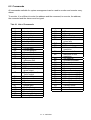
I - 1 - 30/Oct/01
SECTION 4
Protections
power supply
drive module
IV - 1
2
SECTION 5
Adjustment
of T/S curve
phase-speed relation
phase-current relation
parameters setting for FAS T-V
V-1
2
2
SECTION 6
Commands
general features
commands
VI - 1
3
SECTION 7
Troubleshooting
DBM-PS troubleshooting
DBM module troubleshooting
VII -1
4
I - 2 - 30/Oct/01
Accident Protection
The safety instructions provided in this Manual are included to prevent injury to personnel
(WARNINGS) or damage to equipment (CAUTIONS).
WARNING: L+ and L- pins and Bus Bar's can have voltage
≥810Vdc even after switching off (capacitive voltage).
High Voltage - Discharge Time approx. 6 Minutes.
WARNING: High Voltage. The recovery resistor is connected to
the Bus Bar’s and can have voltage ≥810Vdc.
WARNING: do not touch recovery resistor during operation to
avoid scalds.
CAUTION: make sure that the correct input voltage, 400V or 460V, has been set.
CAUTION: it is recommended to disconnect the drive and the EMC filters to carry out
the AC Voltage Tests of EN 60204-1 (1997), par.19.4, in order to not damage the Ytype capacitors between phases and ground. Moreover the DC voltage dielectric test
required by EN 50178 (1997), product family standard, has been carried out in factory
as a routine test. The DC Insulation Resistance Tests of EN 60204-1 (1997), par.19.3,
may be carried out without disconnecting the drive and the EMC filters.
CAUTION: when required for an emergency stop, opening U2-V2-W2 pins and closing
motor phases to resistors, must be preceded by disabling the axis. The delay time
must be at least 30 ms.
CAUTION: in case of repetitive switching on and off, wait 1 minute between off and
on.
CAUTION: it is recommended to close the WP jumper on the Personality Card at the
end of installation and setup.
CAUTION: do not exceed the tightening torque of the table (but see proper data
sheets for the tightening torque of input capacitors and power modules and see
Section 2 of this Manual for the tightening torque of terminal blocks)
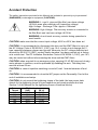
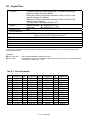
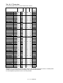
Screw
Thread
M3
M4
M5
M6
M8
Tightening torque
[Nm]
[lb in]
1.00
8.85
3.00
26.55
6.00
53.10
8.00
70.80
20.0
177.0
I - 3 - 30/Oct/01
I - 4 - 30/Oct/01
CE Requirements
• Cautionary Marking. See Accident Protection page.
• Protection against electric shock. Electronic Equipment intended for installation in
closed electrical operating areas kept locked. The lock shall be only opened by authorized
person and the access only allowed to skilled persons whilst energized. Where the
equipment requires manual intervention, 412.2.1 of HD 384.4.41 S2 shall be consulted.
• Fixed connection for protection. The equipment may have a continuous leakage current
of more than a.c. 3.5 mA or d.c. 10 mA in normal use and a fixed ground connection is
required for protection.
• RCD. A d.c. component can occur in the fault current in the event of a fault connection to
earth. Only a residual-current-operated protective device (RCD) of Type B is allowed.
When the protection in installations with regard to indirect contact is achieved by means of
an RCD, their appropriate function/combination shall be verified.
• Climatic Conditions. Equipment intended to operate within its performance specification
over the range of Class 3K3, as defined in table 1 of EN 60721-3-1, EN 60721-3-2, EN
60721-3-3, EN 60721-3-4, partly modified.
• Pollution Degree 2 Installation - The equipment shall be placed in a pollution degree 2
environment, where normally only non-conductive pollution occurs. Occasionally, however,
a temporary conductivity caused by condensation is to be expected, when the electronic
equipment is out of operation.
• EMC Requirements. The installer of the equipment is responsible for ensuring
compliance with the EMC standards that apply where the equipment is to be used.
Product conformity is subjected to filters installation and to recommended procedures, as
from Section 3 of this Manual.
• Second Environment (EMC). Equipment intended to be connected to an industrial lowvoltage power supply network, or public network which does not supply buildings used for
domestic purposes (second environment, according to EMC Standards).
It is not intended to be used on a low-voltage public network which supplies domestic
premises (first environment). Radio frequency interference is expected if used on such a
network.
• Recovery Resistor Cable. Shielding of the external recovery resistor cable, provided in
kit for test purposes, is recommended for ensuring compliance with the EMC standards.
I - 5 - 30/Oct/01
I - 6 - 30/Oct/01
UL Requirements
• These Brushless Servo-Drives shall be assembled with the guidelines specified in this
Manual. Only the configurations with the components tested and described in the UL
Report, file E194181, Vol.2, Sec.1, Issue date 03-28-01 and following Revisions can bear
the Recognized Component (R/C) Mark. Each assembled configuration shall be evaluated
in the UL Listed end-use application.
• The Component – Power Conversion Equipment “DBM 04 Series” is considered UL
Recognized in the complete configurations after the assembly of the three main parts of
the Drive, that is the Power Supply, the Modules and the Fan Assembly. The Marking,
including the R/C Mark and the Drive Model No., shall consider the equipment in its
complete configuration.
• These drives shall be used within their ratings, as specified in the marking of the
equipment. In particular:
- rated input voltage, input current, system duty cycle, auxiliary input voltage, auxiliary
input power, fan input voltage, fan input power on the label affixed on the fan assembly
- rated axis continuous output current, axis max output current, module duty cycle on the
label affixed on the module
• Cautionary Marking. See Accident Protection page.
• Duty Cycle. The maximum continuous Drive output current shall be limited to 65 A and to
the Maximum Module Current, due to the rated current of the Power Supply and of the
Module. According to this reason, the Drive shall be used with a Duty Cycle, as specified
in the marking of the equipment.
• Surrounding Air Temperature - "Maximum Surrounding Air Temperature 40°C". In the
final installation considerations shall be given for the need of repeating Temperature test if
the unit is mounted with a different Surrounding Air conditions.
• Pollution degree 2 Installation - The drive must be placed in a pollution degree 2
Environment.
• Environmental designation - “Open Type Equipment”.
• Short Circuit Ratings. “Equipment suitable for use on a circuit capable of delivering not
more than 5000 rms Symmetrical Amperes, 460 V ac +10% maximum”
• Branch Circuit Protection. The Branch Circuit Protection for Short Circuit shall be
provided in the end-use applications by external R/C Fuses (JFHR2), manufactured by
Bussmann Div Cooper (UK) Ltd, Semiconductor fuse type, Mod.No. 160 FEE, rated 160
A, 660 Vac, 200 kA A.I.C.
I - 7 - 30/Oct/01
• Overspeed Protection. The Power Conversion Equipment is incorporating an Overspeed
Protection. See MV command in Section 6 of this Manual.
• Overvoltage Control. In the equipment the Overvoltage is controlled by a Transient
Suppressive device, with 1500 V Clamping Voltage and min 120 J (10x1000 us or 2 ms)
Energy Handling Capability. See also “Bus not normal” protection in Section 4. of this
Manual
• Overload Protection. The equipment does not incorporate internal overload protection for
the motor load. The drive is intended to be used with motors that must have integral
thermal protection through a PTC. The overtemperature fault of the drive will trip when the
PTC reaches 1.2 kΩ. See J4-J5-J6 connectors in Section 2 of this Manual for wiring.
• Over-Current Protection. The drive is provided with a current limiting circuitry. See IL and
IT commands in Section 6 of this Manual.
• Factory Wiring. These equipments are suitable only for Factory Wiring only, that is the
Terminal Blocks and the Connectors for Power Connection Wiring are not suitable for
Field Wiring. In particular the DC-Bus Terminal Blocks for the Power Supply and Modules
Interconnection shall be usable only with the DC-Bus Interconnection Cables provided by
the manufacturer.
• Wiring. Wiring shall be made by stranded and/or solid, copper (Cu), 60/75°C (140/167°F)
conductor only, and, for terminal blocks, the tightening torque values specified in Section 2
of this Manual shall be applied. These requirements do not pertain to control circuit
terminals.
• Wiring of Recovery Resistor. The Dynamic Brake Unit Recovery Resistor shall have the
connection wiring made with R/C (AVLV2) or insulated with R/C (YDPU2) or R/C (UZCW2)
in the end-use installation.
I - 8 - 30/Oct/01
SECTION 1 - DESCRIPTION
1.1 Description
DBM04 four quadrant servodrives provide unrivaled compactness and flexibility through the
integration of three axes in a single module.
A power supply is connected directly to the power distribution line at 400 or 460V and can
supply up to 6 modules (18 axes). The result is a very suitable solution for all multi-axis
applications like machine tools, robotics, packaging, special material working (wood, plastics,
glass, rubber, leather, paper).
A microprocessor based structure allows high servo performances with FASTACT and FC
servomotors all equipped with a resolver feedback. Drive tuning and configuration are
performed via digital parameters (not potentiometers) and stored in non-volatile memory
(EEPROM).
Drive set up is possible via a keypad or PC, therefore simplifying installation and providing
easy fault diagnosis.
General features:
• digital speed loop
• sinusoidal current waveform
• SMD technology with boards automatically assembled and tested
• automatic Resolver to Digital (R/D) resolution switching (from 16 to 10 bit) to achieve high
motion accuracy in the whole speed range (from 0 to 10000 RPM).
• up to 99 axis system configuration
• 10 kHz switching frequency
• operating temperature: 0 to +40°C (exceeding Class 3K3)
• relative humidity: 5% to 85% (no condensation, no formation of ice)
• air pressure: 86 kPa to 106 kPa
• storage temperature: -25 to +55°C (Class 1K4)
• transportation temperature: -25 to +70°C (Class 2K3)
• immunity to vibration: Class V.H.2 according to HD 413.3 S1 (1987)
• maximum case depth of 310 mm
1.2 Electrical Data
PS-Standard Power Supply
•
•
•
•
•
3-phase power input voltage: 400 or 460 Vac (selectable via switch), ±10%, 50/60 Hz
1-phase auxiliary input voltage: 110 or 230 Vac (selectable via jumper), ±10%, 50/60 Hz
input current: 65 A
output current: see tab. 1.1
max number of modules supplied: 4
I - 9 - 30/Oct/01
PS-6M Power Supply (Standard Plus)
•
•
•
•
•
3-phase power input voltage: 400 or 460 Vac (selectable via switch), ±10%, 50/60 Hz
1-phase auxiliary input voltage: 110 or 230 Vac (selectable via jumper), ±10%, 50/60 Hz
input current: 65 A
output current: see tab. 1.1
max number of modules supplied: 6
PS-Standalone Power Supply
•
•
•
•
•
3-phase power input voltage: 400 Vac or 460 Vac (set in factory), ±10%, 50/60 Hz
1-phase auxiliary input voltage (for data saving): 230 Vac, ±10%, 50/60 Hz
input current: 65 A
output current: see tab. 1.1
max number of modules supplied: 4
PS-120 Power Supply (Powered Standalone)
•
•
•
•
•
3-phase power input voltage: 400 Vac or 460 Vac (set in factory), ±10%, 50/60 Hz
1-phase auxiliary input voltage (for data saving): 230 Vac, ±10%, 50/60 Hz
input current: 120 A
output current: see tab. 1.1
max number of modules supplied: 4
PS-U Power Supply (Special Standalone)
•
•
•
•
•
3-phase power input voltage: 400 to 460 Vac, ±10%, 50/60 Hz
auxiliary input voltage (for data saving): 24 Vdc, ±10%
input current: 65 A
output current: see tab. 1.1
max number of modules supplied: 4
DBM 04 Module
• BUS BAR rated voltage: 540 Vdc (with 400 Vac) or 620 Vdc (with 460 Vac)
• three-phase output voltage: 325 Vac (with 400 Vac) or 375 Vac (with 460 Vac)
• output current: see tab. 1.1
DBM 04 Fan Assembly
• input voltage: 230 Vac or 115 Vac, +6%/-10%, 50/60 Hz, or 24 Vdc, ±4%
• input power: see tab. 2.1
I - 10 - 30/Oct/01
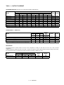
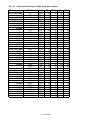
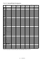
TAB. 1.1 - OUTPUT CURRENT
STANDARD MODULES (see tab.2.16 for the other possible configurations)
Model
Rated
(Arms)
DBM 04 3-3
DBM 04 6-6
DBM 04 8-8
DBM 04 15-15
DBM 04 25-25
DBM 04 35-35*
DBM 04 3-3-3
DBM 04 6-6-6
DBM 04 8-8-8
DBM 04 15-15-15
Output Current
Axis 2
Axis 1
Max
(Arms)
(A)
3
6
8
15
25
35
3
6
8
15
6.4
10.6
15.6
29.7
49.5
63.6
6.4
10.6
15.6
29.7
9
15
22
42
70
90
9
15
22
42
Rated
(Arms)
3
6
8
15
25
35
3
6
8
15
Axis 3
Max
(Arms)
(A)
6.4
10.6
15.6
29.7
49.5
63.6
6.4
10.6
15.6
29.7
Rated
(Arms)
9
15
22
42
70
90
9
15
22
42
3
6
8
15
Width
Max
(Arms)
(A)
6.4
10.6
15.6
29.7
9
15
22
42
Weight
(mm)
(kg)
120
120
120
120
180
270
120
120
120
180
8
8
8
9
13
18
9
9
9
14
* a duty cycle of 92% applies
POWER SUPPLY - 400/460 Vac
Current
Model
Output
Rated
(A)
Output
Max
(A)
Braking
(A)
65
65
65
120
65
100
100
100
280
100
100
100
100
175
100
PS-Standard Power Supply
PS-6M Power Supply (Standard Plus)
PS-Standalone Power Supply
PS-120 Power Supply (Powered Standalone)
PS-U Power Supply (Special Standalone)
Auxiliary
Input
Voltage
(V)
110/230 Vac
110/230 Vac
230 Vac*
230 Vac*
24 Vdc*
Width
Weight
(mm)
(kg)
120
120
120
180
120
13
13
13
20
13
* this is not necessary for normal duty but only for data saving
EXPANSIONS
An external expansion module should be used for some configurations, including an axis rated over 35A. This is due to thermal
constrictions.
Available expansions modules are shown in the table. To specify an expansion module, please replace the third axis rating number with E,
this ensures that the drive is configured for use with an expansion module (e.g. DBM 04 15-15-E).
Output Current
Model
EBM 04 50/140
EBM 04 60/180
Rated
(Arms)
Width
Weight
(A)
Max
(A)
(mm)
(kg)
50
60
99
127
140
180
270
270
18
18
I - 11 - 30/Oct/01
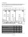
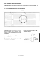
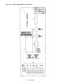
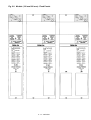
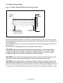
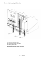
1.3 Dimensions
Fig. 1.1 and 1.2 (dimensions in mm) show the drilling jig between power supply and drive
module. The modules must be mounted vertically, with the fan housing at the bottom. Leave a
clear space of at least 50 cm (19.7 in) over and under the system for air circulation.
Fig. 1.1 Front View (Drill For M5 Screws)
Power
Supply
120 mm
DBM 04
DBM 04
DBM 04
120 mm
Module
180 mm
Module
270 mm
Module
Configuration
1 DBM04 PS + 1 DBM04 120 mm
1 DBM04 PS + 1 DBM04 180 mm
1 DBM04 PS + 2 DBM04 120 mm
1 DBM04 PS + 1 DBM04 270 mm
1 DBM04 PS + 1 DBM04 120 mm + 1 DBM04 180 mm
1 DBM04 PS + 2 DBM04 180 mm
1 DBM04 PS + 3 DBM04 120 mm
1 DBM04 PS + 1 DBM04 120 mm + 1 DBM04 270 mm
1 DBM04 PS + 2 DBM04 120 mm + 1 DBM04 180 mm
1 DBM04 PS + 1 DBM04 180 mm + 1 DBM04 270 mm
1 DBM04 PS + 1 DBM04 120 mm + 2 DBM04 180 mm
1 DBM04 PS + 4 DBM04 120 mm
L
241
301.5
362
391
422.5
483
483
512
543.5
572.5
604
604
L1
266
326
387
416
447
508
508
537
568
597
629
629
L2
282
342
403
432
463
524
524
553
584
613
645
645
Note: the width of the Power Supply PS-120 is 180 mm. Contact our Sales Locations or Service Centers for the
available configurations and dimensions with this Power Supply.
I - 12 - 30/Oct/01
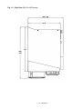
Fig. 1.2 Side View (Drill For M5 Screws)
I - 13 - 30/Oct/01
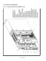
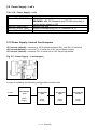
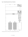
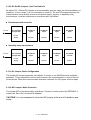
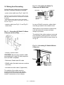
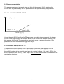
1.4 Component Identification
Fig. 1.3 Component Identification (DBM 04 15-8-8)
I - 14 - 30/Oct/01
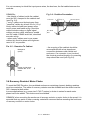
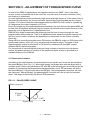
1.5 System Grounding
Fig. 1.4 EMC/Equipotential Bonding
I - 15 - 30/Oct/01
1.6 Options
• software programmable (from 128 to 16384 pulses per electrical revolution) simulated
encoder with marker
• A/D 14 bit converter on the speed reference with the possibility of software choice
between 12 bit standard conversion and 14 bit optional conversion
• R/D converter resolution: 8 arc/min 2-axis, 4 arc/min 2-axis, 2 arc/min 2-axis,
8 arc/min 3-axis, 4 arc/min 3-axis, 2 arc/min 3-axis
• installation and setup keypad
• PC communication package: see par. 2.11.2.1
• ADR function: external 24 Vdc UPS with added capacitance to recover braking energy
(see Application Note GB-4528)
• frequency reference to use a velocity reference generated by Pulse Frequency
Modulation (PFM) from 0 to 100 kHz instead of the standard analog signal (see
Application Note I-4521)
• master-slave (electric shaft) special software for DBM 04 with expansion (see Application
Note GB-4527)
1.7 Rating Plate
The following informations are supplied on the rating plate of DBM 04.
1.7.1 Power Supply
CODE:
S/N:
Vin:
50/60 Hz
Iin:
Iout nom:
Iout max:
CYZZZZ
AASS NNNNNN
xxx V
3-phase
xxx Arms
xxx Arms
xxx A
where ZZZZ=model code
where AA=year, SS=week, NNNNNN=serial number
nominal three phase input voltage
nominal rms input current
nominal rms output current
peak output current
I - 16 - 30/Oct/01
1.7.2 Module
CODE:
S/N:
3-phase
D.C.:
CY1ZZZ XX
AASS NNNNNN
where 1ZZZ=model code; XX=option code
where AA=year, SS=week, NNNNNN=serial number
XXX%
Axis 1
Iout nom
Iout max
Axis 2
Iout nom
Iout max
Axis 3
Iout nom
Iout max
C1C2C3-C4
XX Arms
YYY A
C1C2C3-C4
XX Arms
YYY A
C1C2C3-C4
XX Arms
YYY A
module duty cycle, related to the max nominal current of the
module (34A for 120mm, 53A for 180mm, 65A for 270mm)
code for motor, resolver, simulated encoder (see below)
nominal rms output current
peak output current
code for motor, resolver, simulated encoder (see below)
nominal rms output current
peak output current
code for motor, resolver, simulated encoder (see below)
nominal rms output current
peak output current
C1C2C3-C4
C1=pulses per electrical revolution (C=64, D=128, E=256, F=512,
G=1024, H=2048, I=4096, L=8192, M=16384)
C2=motor poles (A=2, B=4, C=6, D=8, E=10, F=12)
C3=resolver poles (A=2, B=4, C=6, D=8, E=10, F=12)
C4 =marker width (A=1, B=1/2, C=1/4, D=no marker)
1.7.3 UL Rating Plate
To comply with the UL requirements, the following data are shown on the rating plate of the
Fan Assembly. These data are referred to the complete DBM 04 system, UL Recognized,
that is Power Supply, one or more modules, fan assembly.
The Duty Cycle is related to the max nominal current of the Power Supply (65A for PSStandard, PS-Standalone and PS-U).
The Flow Rate (F.R.) is the sum of the fan flow rates of the fan assembly.
Power Supplies and modules intended to be part of a complete DBM 04 system, UL
Recognized, are marked “Part of a Recognized System”.
Example:
CODE
CY2000 - CY2007 A0 - CY1200 A2 - CY1200 A9 - CY1200 A9 - CY4200
Vin 400 Vac
3-phase
50/60Hz
27 Arms - Duty Cycle 100 %
Iin
Vin 110/230 Vac
Auxiliary Input
240
W
Pin
Fan Assembly
Vin 115
Vac
Pin
56 W
F.R. 560
m3/h
I - 17 - 30/Oct/01
This page intentionally blank
I - 18 - 30/Oct/01
SECTION 2 - INSTALLATION
CAUTION: make sure that the correct input voltage, 400V or 460V, has been set.
Fig.2.1 PS-Standard and PS-6M - 400/460V Setting
Top Panel
CAUTION: make sure that the correct
wiring has been set for auxiliary input
voltage on the PS-Standard and PS-6M
front panel.
Fig.2.2 PS-Standard and PS-6M 110/230V Jumper
- connect the jumper on J12 connector
to use 110 Vac
or
- disconnect the jumper on J12
connector to use 230 Vac
II - 1 - 30/Oct/01
2.1 Fuses
2.1.1 Internal Auxiliary Fuses
2.1.1.1 PS-Standard and PS-6M
A delayed type fuse, rated 4A/250V, is provided on the front panel, to protect the auxiliary
power circuit. The following types are approved:
- Mod.No.SPT 0001.2510 by Schurter AG
- Mod.No. ST520240 by Bussmann Div Cooper (UK) Ltd
2.1.1.2 PS-Standalone and PS-120
A delayed type fuse, rated 3.15A/250V, is provided on the internal base card, to protect the
auxiliary power circuit. The following types are approved:
- Mod.No.SPT 0001.2509 by Schurter AG
- Mod.No. ST520231 by Bussmann Div Cooper (UK) Ltd
2.1.2 External Power Fuses (one in each phase of the power line)
2.1.2.1 PS Standard, PS-6M, PS-Standalone and PS-U
CAUTION: equipment suitable for use on a circuit capable of delivering not more than
5000 RMS symmetrical Amperes, 460V +10% maximum, when protected by
semiconductor type fuses, mod.No.160-FEE, manufactured by Bussmann Div.Cooper
(UK) Ltd
2.1.2.2 PS-120
Semiconductor type fuses, mod.No.315-FM (315A/660Vac), manufactured by Bussmann
Div.Cooper (UK) Ltd, are recommended.
2.2 Soft Start
The soft start circuit (inrush current limiting) is built-in.
II - 2 - 30/Oct/01
2.3 Transformers
2.3.1 Power Transformer
The system is designed to allow direct operation from a 400/460 Vac three phase power line,
without isolation transformer. An isolation transformer may still be required to meet local safety
regulations. It is the user responsibility to determine if an isolation transformer is required to
meet these requirements.
To size the power transformer It is necessary to refer to the rated output power of the motors
(the output power with 65K winding overtemperature is included in the Technical Data table of
catalogs of servomotors), to sum the power of single axes, to multiply the sum by the
contemporaneity factor (factors often utilized are Kc=0.63 for 2 axes, Kc=0.5 for 3 axes,
Kc=0.38 for 4 axes, Kc=0.33 for 5 axes, Kc=0.28 for 6 axes), and by a correction coefficient
(=1.2), accounting for the losses of the motor/drive system.
P = Σ Pim ∗ Kc ∗ 1.2
[W]
2.3.2 Auxiliary Power Transformer - PS-Standard and PS-6M
A transformer for the auxiliary line is not necessary.
2.3.3 Auxiliary Power Transformer - PS-Standalone and PS-120
If data need to be saved in case of three phase power line failure, a 230 Vac monophase
auxiliary line must be connected, via isolation transformer, to the PS-Standalone and PS-120
versions of Power Supply. This is not necessary for normal duty but only for data saving.
CAUTION: do not connect directly the auxiliary line but only through a dedicated,
isolation transformer with 230Vac ±10%, 50/60 Hz secondary voltage. Rated power
must be 60VA for each module (e.g. 240VA for 4 modules)
2.4 Thermal sizing of cabinet
To calculate cabinet cooling requirements, table below provides estimated equipment power
dissipation values. If the application employs continuous braking, it is necessary to include
the recovery resistor power dissipation (use the nominal power of recovery resistor if actual
application recovery dissipation is unknown).
PS-Standard
PS-6M
PS-Standalone
PS-U
25 W
Power Dissipation
PS-120 Module IGBT's
50 W
50 W
16 W/A
Input
Bridge
1 W/A
Example: with one PS-Standard, two modules, a total output current of 60 Arms and
continuous unknown braking, the dissipated power is as follows.
Pd = 25 + (2 ∗ 50) + (16 ∗ 60[A]) + (1 ∗ 60[A]) + 750 [recovery resistor power] = 1895 W
II - 3 - 30/Oct/01
2.5 Recovery Circuit
The recovery circuit is formed by a switching regulator, a recovery transistor and a recovery
resistance. While braking the motor returns energy which cannot be sent to the line since the
rectifier circuit is not regenerative. Returned energy tends to increase the BUS BAR DC
voltage. When HV reaches 680V (for 400Vac version) or 790V (for 460V version) the
switching regulator brings the recovery transistor into conduction, thus connecting the
recovery resistance in parallel with filter capacitors. The recovery resistance is formed by
enameled wire fixed resistor(s).
If the recovery resistance works for intervals shorter than the time necessary to reach
thermal equilibrium, the resistor can temporarily handle power levels up to 10 times the
nominal power rating of the resistor (short time overload).
If not specifically requested, PS-Standard, PS-6M, PS-Standalone are provided with 8.2 Ω,
750W recovery resistor, while PS-U is provided with 12 Ω, 750W recovery resistor and PS120 with 3.9 Ω, 1000W recovery resistor.
WARNING: High Voltage. The recovery resistor is connected to the Bus Bar’s and can
have voltage ≥810Vdc
WARNING: do not touch recovery resistor during operation to avoid scalds.
CAUTION: an unusual application with motor driven by the load, a large portion of the
time, could result in overheating of the recovery resistor.
An unusual application with motor driven by high inertial load from high velocity in very
short deceleration time could require a non standard recovery resistor.
It is suggested contacting our Service Centers.
CAUTION: shielding of the recovery resistor cable, provided in kit for test purposes, is
recommended for ensuring compliance with the EMC standards.
CAUTION: for UL approval in the end-use installation, the Dynamic Brake Unit
Recovery Resistor shall have the connection wiring made with R/C (AVLV2) or
insulated with R/C (YDPU2) or R/C (UZCW2)
II - 4 - 30/Oct/01
2.6 Fan Assembly
The ventilation is provided by fans mounted under the modules. The size and the number of
fans are according to the system configuration. Selection of the correct Fan Assembly is due
by matching Fan Assembly width to the total of the DBM drives package (i.e. Fan = Power
Supply and DBM module(s) and DBM expansion module(s)).
Fan input voltage is 230 Vac or 115 Vac or 24 Vdc.
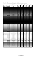
TAB. 2.1 - FAN ASSEMBLY
Model Code
Fan Assembly
Width
mm
Input
Voltage
V
Input
Power
W
CY4300, CY4318, CY4359, CY4360
CY4301, CY4323, CY4337, CY4338
CY4302, CY4319, CY4339, CY4340
CY4303, CY4341, CY4342
CY4304, CY4320, CY4334, CY4343, CY4344
CY4305, CY4321, CY4331, CY4335, CY4345, CY4346
CY4306, CY4316, CY4347, CY4348
CY4307, CY4311, CY4349, CY4350
CY4308, CY4351, CY4352
CY4309, CY4312, CY4324, CY4336, CY4353, CY4354
CY4310, CY4355, CY4356
CY4315, CY4357, CY4358
CY4100, CY4118, CY4159, CY4160
CY4101, CY4123, CY4137, CY4138
CY4102, CY4119, CY4139, CY4140
CY4103, CY4141, CY4142
CY4104, CY4120, CY4134, CY4143, CY4144
CY4105, CY4121, CY4131, CY4135, CY4145, CY4146
CY4106, CY4116, CY4147, CY4148
CY4107, CY4111, CY4149, CY4150
CY4108, CY4151, CY4152
CY4109, CY4112, CY4124, CY4136, CY4153, CY4154
CY4110, CY4155, CY4156
CY4115, CY4157, CY4158
CY4200, CY4213, CY4214
CY4201, CY4215, CY4216
CY4202, CY4217, CY4218
CY4203, CY4219, CY4220
CY4204, CY4221, CY4222
CY4205, CY4211, CY4223, CY4224
CY4206, CY4225, CY4226
CY4207, CY4227, CY4228
CY4208, CY4229, CY4230
CY4209, CY4212, CY4231, CY4232
CY4210, CY4233, CY4234
CY4235, CY4236
240
300
360
390
420
480
510
540
570
600
750
660
240
300
360
390
420
480
510
540
570
600
750
660
240
300
360
390
420
480
510
540
570
600
750
660
24 Vdc
24 Vdc
24 Vdc
24 Vdc
24 Vdc
24 Vdc
24 Vdc
24 Vdc
24 Vdc
24 Vdc
24 Vdc
24 Vdc
230 Vac
230 Vac
230 Vac
230 Vac
230 Vac
230 Vac
230 Vac
230 Vac
230 Vac
230 Vac
230 Vac
230 Vac
115 Vac
115 Vac
115 Vac
115 Vac
115 Vac
115 Vac
115 Vac
115 Vac
115 Vac
115 Vac
115 Vac
115 Vac
23
46
46
46
57
69
69
69
69
92
92
92
64
128
128
128
147
192
192
192
192
256
256
256
56
112
112
112
130
168
168
168
168
224
224
224
CAUTION: a free circulation must be guaranteed for the air flow.
II - 5 - 30/Oct/01
Total
Flow
Rate
m3/h
520
1040
1040
1040
1200
1560
1560
1560
1560
2080
2080
2080
485
970
970
970
1130
1455
1455
1455
1455
1940
1940
1940
560
1120
1120
1120
1300
1680
1680
1680
1680
2240
2240
2240
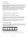
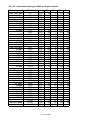
2.7 Wire Type
2.7.1 Sizing of Wires
It is recommended to use Cu, stranded and/or solid wires, 60/75°C (140/167 °F), UL
approved, per the following table.
Note that in the table the wires are sized according to the nominal current. The wires can be
undersized if the actual rms current of the application is lower.
Tab. 2.2 - Sizing of Wires
Notes
DBM 04 Model
Power Supply
PS-Standard, PS-6M,
PS-120
3/9 to
PS-U, PS-Standalone
15/42
4x
4x
6 AWG
2 AWG
2x
2x
.
14 AWG
10 AWG
.
.
4x
14 AWG
2x
2x
.
10 AWG
6 AWG
8 AWG (provided in kit)
Power Line and ground
wiring (No.of wires x AWG)
Auxiliary Line wiring
(No. of wires x AWG)
Motor Power wiring
(No.of wires x AWG)
Recovery Resistor wiring
(No.of wires x AWG)
Dc-Bus (+/-AT)
Resolver wiring
(No.of wires x AWG)
-
Axis
25/70
-
-
35/90 to
60/180
-
-
.
-
-
8x
14 AWG
.
4x
6 AWG
.
shielded
shielded
with 4 pair,
each pair
twisted and
individually
shielded with
an
independent
overall shield
4 x 2 x 22/20 AWG
Tab. 2.3 - AWG/mm2 Conversion Table
AWG
mm2
22
0.3
20
0.5
18
0.8
16
1.3
14
2.1
12
3.3
10
5.3
8
8.4
6
13
4
21
3
27
2
34
1
42
1/0
54
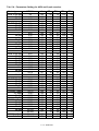
Tab. 2.4 - Tightening torque of Power Connectors/Terminal Blocks
Mfg
lb in
Nm
Moog
DC-Bus
53
6
Phoenix Contact Gmbh
HDFK 4
HDFK 10
HDFK 25
5-7
13.2-16
35
0.6-0.8
1.5-1.8
4
Harting Kgaa
Han16E
HanK 4/0
4.4
7
0.5
0.8
Tab. 2.5 - Wire stripping length for Power Connectors/Terminal Blocks
in
mm
HDFK 4
0.35
9
Phoenix Contact Gmbh
HDFK 10
HDFK 25
0.43
0.75
11
19
II - 6 - 30/Oct/01
Harting Kgaa
Han16E
HanK 4/0
0.28
0.55
7
14
Wago Gmbh
231-104
0.33
8-9
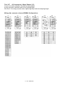
Fig. 2.3A Power Supply - Front Panels
PS-Standalone
PS-Standard and PS-6M
II - 7 - 30/Oct/01
Fig. 2.3B Power Supply PS-120 - Front Panel
II - 8 - 30/Oct/01
Fig. 2.3C Power Supply PS-U - Front Panel
II - 9 - 30/Oct/01
2.8 Power Supply - Wiring
See Par.2.7 for sizing of power wires, tightening torque and wire stripping length. See Section 3
for shielding procedures according to EMC Directive.
2.8.1 Signal/ Auxiliary Wiring
Tab. 2.6 - Power Supply - J1 Conn. - Auxiliary Power Supply (to Modules)
Panel side: shrouded header with 13 male contacts
Wiring side: connector with 13 female contacts (provided in kit with cable)
Pos.
1
2
3
4
5
6
7
8
9
10
11
12
13
Function
Not connected (N.C.)
+18Vdc referred to -HV (540/620 Vdc)
-HV (540/620 Vdc)
158kHz square wave to high side drives
N.C.
N.C.
+18Vdc referred to logic 0V
- 18Vdc referred to logic 0V
+8Vdc referred to logic 0V
+8Vdc referred to logic 0V
Logic 0V
Resolver 0V
10 kHz sinusoidal wave for resolver and synchronism (carrier)
Tab. 2.7 - Power Supply - J2 Conn. - RS485 Port/Fault signals (to Modules)
Panel side: Sub-D with 9 male contacts
Wiring side: Sub-D with conductive shell, 9 female contacts (supplied with cable)
Pos.
1
2
3
4
5
6
7
8
9
Function
+ Rx (RS485 serial link)
N.C.
+ Tx (RS485 serial link)
Power supply binary coded faults (see Tab.2.8)
+ 5Vdc input referred to logic 0V
- Rx (RS485 serial link)
Logic 0V
- Tx (RS485 serial link)
Power supply binary coded faults (see Tab.2.8)
Tab. 2.8 - Power Supply binary coded faults
J2/pos. 4
0
0
1
1
J2/pos. 9
0
1
0
1
OK
DBR FAULT. Recovery fault
OVER TEMP. Overtemperature
Not Used.
II - 10 - 30/Oct/01
Tab. 2.9 - Power Supply - J10 Connector - RS485 Port (to keypad or to converter)
Panel side: Sub-D with 9 female contacts
Wiring side: Sub-D with 9 male contacts (supplied with the optional RS232/485 converter kit
or with the optional keypad)
Pos.
1
2
3
4
5
6
7
8
9
Function
+Rx (RS485 serial link)
N.C.
+Tx (RS485 serial link)
N.C.
+5Vdc output referred to logic 0V for power supply
-Rx (RS485 serial link)
Logic 0V
-Tx (RS485 serial link)
N.C.
2.8.2 Power Wiring
2.8.2.1 PS-Standard and PS-6M
Tab. 2.10 - J11 Connector - Power
Power: Terminal Blocks Mod.No.HDFK 10 by Phoenix Contact Gmbh
See Par.2.7 for sizing of power wires, tightening torque and wire stripping length
Name
U1
V1
W1
Function
"L1" phase, three-phase input voltage 400Vac (or 460Vac)
"L2" phase, three-phase input voltage 400Vac (or 460Vac)
"L3" phase, three-phase input voltage 400Vac (or 460Vac)
Ground
R.R.
R.R.
Recovery resistor
Recovery resistor
Tab. 2.11 - J12 Connector - Aux Power
Panel side: shrouded open end header with 4 male contacts
Wiring side: connector Mod.No.231-104/026-000 by Wago Gmbh (provided in kit)
See Par.2.7 for sizing of power wires, tightening torque and wire stripping length
Name
AUX PWR
JUMPER
JUMPER
AUX PWR
Function
Auxiliary power supply 230Vac/110Vac
Jumper (see Fig.2.2)
Open=230Vac - Closed=110Vac
Auxiliary power supply 230Vac/110Vac
II - 11 - 30/Oct/01
2.8.2.2 PS-Standalone
Tab. 2.12 - J11 Connector - Power
Aux Power: Terminal Blocks Mod.No.HDFK 4 by Phoenix Contact Gmbh
Power: Terminal Blocks Mod.No.HDFK 10 by Phoenix Contact Gmbh
See Par.2.7 for sizing of power wires, tightening torque and wire stripping length
Name
AUX PWR
AUX PWR
U1
V1
W1
Function
Auxiliary power supply 230Vac
Auxiliary power supply 230Vac
"L1" phase, three-phase input voltage 400Vac (or 460Vac)
"L2" phase, three-phase input voltage 400Vac (or 460Vac)
"L3" phase, three-phase input voltage 400Vac (or 460Vac)
Ground
R.R.
R.R.
Recovery resistor
Recovery resistor
2.8.2.3 PS-120
Tab. 2.13 - J11 Connector - Power
Aux Power: Terminal Blocks Mod.No.HDFK 4 by Phoenix Contact Gmbh
Power: Terminal Blocks Mod.No.HDFK 25 by Phoenix Contact Gmbh
See Par.2.7 for sizing of power wires, tightening torque and wire stripping length
Name
AUX PWR
AUX PWR
U1
V1
W1
Function
Auxiliary power supply 230Vac
Auxiliary power supply 230Vac
"L1" phase, three-phase input voltage 400Vac (or 460Vac)
"L2" phase, three-phase input voltage 400Vac (or 460Vac)
"L3" phase, three-phase input voltage 400Vac (or 460Vac)
Ground
R.R.
R.R.
Recovery resistor
Recovery resistor
II - 12 - 30/Oct/01
2.8.2.4 PS-U
Tab. 2.14 - J11 Connector - Power
Aux Power: Terminal Blocks Mod.No.HDFK 4 by Phoenix Contact Gmbh
Power: Terminal Blocks Mod.No.HDFK 10 by Phoenix Contact Gmbh
See Par.2.7 for sizing of power wires, tightening torque and wire stripping length
Name
AUX PWR
AUX PWR
U1
V1
W1
Function
Auxiliary power supply 24Vdc
Auxiliary power supply 24Vdc
"L1" phase, three-phase input voltage 400Vac (or 460Vac)
"L2" phase, three-phase input voltage 400Vac (or 460Vac)
"L3" phase, three-phase input voltage 400Vac (or 460Vac)
Ground
R.R.
R.R.
Recovery resistor
Recovery resistor
Tab. 2.15 - J12 Connector - Safety
Panel side: shrouded open end header with 6 male contacts
Wiring side: connector Mod.No.231-106/026-000 by Wago Gmbh (provided in kit)
Pos.
1
2
3
4
Name
OUTPUT
SAFE 24V-1A
SIGNAL
DC-BUS LOW
5
AUX EXT
6
CONTACT
Function
24Vdc (max 1A) output to feed an external relay during
the anti-freewheeling. See Fig.2.4
Output signal for safety. When the opto is OFF (∞ Ω) the DCBus is over 48V. When the opto is ON (2.7kΩ) the DC-Bus is
under 48V. See Fig.2.4
Input signal for safety. Normally connected to 24 Vdc. When
not
connected to 24 Vdc, the DC-Bus is discharged via the
recovery resistor. See Fig.2.4
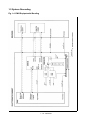
Fig. 2.4 - J12 Connector - Internal Circuitry
II - 13 - 30/Oct/01
2.9 Power Supply - Led's
Tab. 2.16 - Power Supply - Led's
Name
Yellow LED - PWR-BUS
Function
BUS BAR voltage > 40Vdc
WARNING: with PS-Standard and PS-6M, active only if
the aux power supply is ON
Red LED - DBR FAULT
Recovery unit fault
Red LED - OVER TEMP
Module overtemperature via PTC (threshold 70 °C)
Green LED - AUX POWER Auxiliary power supply OK
2.10 Power Supply - Internal Card Jumpers
JP1 closed (default) = connects a 120 Ω resistor between RX+ and RX- of serial link.
JP2 closed (default) = connects TX- of serial link to 0V via pull-down resistor
JP3 closed (default) = connects TX+ of serial link to +5V via pull-up resistor
Fig. 2.5 - Power Supply - Card Jumpers
In case of multidrop, the following configuration must be used.
To user
JP1,JP2,JP3
open
JP1,JP2,JP3
open
JP1,JP2,JP3
open
JP1,JP2,JP3
closed
Power
Supply
Power
Supply
Power
Supply
Power
Supply
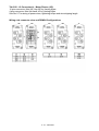
II - 14 - 30/Oct/01
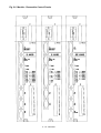
Fig. 2.6 Module - Removable Control Panels
II - 15 - 30/Oct/01
Fig. 2.7 Expansion-EBM - Removable Control Panel
II - 16 - 30/Oct/01
Fig. 2.8 Module (120 mm/180 mm) - Fixed Panels
II - 17 - 30/Oct/01
Fig. 2.9 Module/ Expansion (270 mm) - Fixed Panel
Note: the grey connectors are mounted only in some configurations (see tab.2.27 and 2.28)
II - 18 - 30/Oct/01
2.11 Module Wiring
See Par.2.7 for sizing of power wires, tightening torque and wire stripping length. See Section 3
for shielding procedures according to EMC Directive.
Tab. 2.17 - Module - J1 Connector - Auxiliary Power Supply (to PS/Modules)
Panel side: shrouded header with 13 male contacts
Wiring side: connector with 13 female contacts (supplied in kit with cable)
Pos.
1
2
3
4
5
6
7
8
9
10
11
12
13
Function
Not connected (N.C.)
+18Vdc referred to -HV (540/620 Vdc)
-HV (540/620 Vdc)
158kHz square wave to high side drives
N.C.
N.C.
+18Vdc referred to logic 0V
- 18Vdc referred to logic 0V
+8Vdc referred to logic 0V
+8Vdc referred to logic 0V
Logic 0V
Resolver 0V
10 kHz sinusoidal wave for resolver and synchronism (carrier)
Tab. 2.18 - Module - J2 Connector - RS485 Port/Fault signals (to PS/Modules)
Panel side: Sub-D with 9 male contacts
Wiring side: Sub-D with conductive shell, 9 female contacts (supplied by with cable)
Pos.
1
2
3
4
5
6
7
8
9
+Rx
N.C.
+Tx
Power supply binary coded faults (see Tab.2.19)
+5Vdc output referred to logic 0V
-Rx
logic 0V
-Tx
Power supply binary coded faults (see Tab.2.19)
Tab. 2.19 - Module - Power supply binary coded faults
J2/pos. 4 J2/pos. 9
0
0
0
1
1
0
1
1
OK
DBR FAULT. Recovery fault
OVER TEMP. Overtemperature
Not Used
II - 19 - 30/Oct/01
2.11.1 Limit Switches/Expansion Wiring
The J3 connector allows, when the Expansion is not present, the availability of CW/CCW
limit switches for each axis. With the input enabled (to 0V), the rotation is disabled in one
direction and enabled in the other direction.
When the Expansion is present, the J3 connector is used for signal connection to the
Expansion module.
Fig. 2.10 - Limit Switches Wiring
DBM 04
1
0V
2
CW Limit switch axis 1
5
CCW Limit switch axis 1
6
CW Limit switch axis 2
12
CCW Limit switch axis 2
13
CW Limit switch axis 3
14
CCW Limit switch axis 3
cable shield must be RF*
connected to ground
J3
grounding of shield
via connector shell
*=see Section 3
II - 20 - 30/Oct/01
Tab. 2.20 - Module - J3 Connector - Limit Switches (When EBM Expansion Is Not
Panel side: Sub-D with 15 female contacts
Present)
Wiring side: Sub-D with conductive shell, 15 male solder contacts
Pos.
1
2
3
4
5
6
7
8
9
10
11
12
13
14
15
0V common
CW limit switch, axis 1
N.C.
N.C.
CCW limit switch, axis 1
CW limit switch, axis 2
N.C.
N.C.
N.C.
N.C.
N.C.
CCW limit switch, axis 2
CW limit switch, axis 3
CCW limit switch, axis 3
0V common
Tab. 2.21 - Module/Expansion - J3 Connector - Expansion Connection
Panel side: Sub-D with 15 female contacts
Wiring side: Sub-D with conductive shell, 15 male solder contacts
Pos.
1
2
3
4
5
6
7
8
9
10
11
12
13
14
15
0V common
Auxiliary voltages referred to logic 0V not OK signal
Phase U reference current signal
Torque enabled signal
Short circuit signal
Overtemperature signal
Expansion present signal
Overtemperature signal
N.C.
Phase V reference current signal
Overtemperature signal
N.C.
BUS BAR fault signal
Auxiliary voltages referred to - HV (540/620 Vdc) not OK signal
N.C.
II - 21 - 30/Oct/01
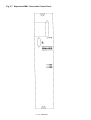
2.11.2 Resolver Wiring
Fig. 2.11 - Resolver Wiring
cosϕ
cosϕ
sinϕ
sinϕ
PTC
PTC
0V
V-Ref
grounding of shield via
connector shell
grounding of shield via
connector clamp
RESOLVER CONNECTOR,
MOTOR SIDE
Signal
FAS T/ FAS N
Type
FAS K
Pos.
Pos.
C
1
cosϕ
E
2
cosϕ
V-Ref
D
10
0V
B
7
PTC
N
8
PTC
A
9
G
11
sinϕ
H
12
sinϕ
shield
S
3
II - 22 - 30/Oct/01
Each DBM module can be connected up to 3 resolvers. Axis 1 resolver must be connected to
J4 M1 connector, axis 2 resolver to J5 M2 and axis 3 resolver to J6 M3.
Figure 2.11 shows the wiring lay-out of the resolver with differential output.
We recommend to use 4 pair cables, each pair twisted and individually shielded with an
independent overall shield. 20 AWG (0.60 mm²
²) or 22 AWG (0.38 mm²
²) wire with low
capacitance can be used. We suggest to use ground connections as shown in Fig. 2.11.
Cable length should not exceed 30 m (100 ft.). It is recommended that the signal cable and
power cable be separated, if possible, through the use of independent duct (conduit) or by a
distance of 12 inches (30 cm).
See Section 3 for shielding procedures according to EMC Directive.
Tab. 2.22 J4-J5-J6 Connectors - Resolvers
Panel side: Sub-D with 9 female contacts
Wiring side: Sub-D with conductive shell, 9 male solder contacts
Pos.
1
Name
cos
2
3
4
Differential cos signal inverted input
cos
Shield
sin
5
6
7
8
9
Differential cos signal non-inverted input
Internally connected to 0V common
Differential sin signal non-inverted input
Differential sin signal inverted input
sin
PTC
0V
PTC
V ref
Motor PTC input
0V common. Special for 10kHz carrier
Motor PTC input
20 Vpp/ 10kHz sinusoidal output signal for supplying primary
resolver winding (carrier)
II - 23 - 30/Oct/01
2.11.3 I/O Wiring
All the signal cables must be separated from power cables by a distance ≥30 cm.
See Section 3 for shielding procedures according to EMC Directive.
REMARKs:
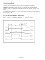
• DRIVE OK (J7 connector): it is suggested to connect the isolated output " DRIVE OK " to
a remote control switch so that, if a fault occurs, the power supply is disconnected to avoid
system damages.
• SIMULATED ENCODER SIGNALS (J7 connector):
- in specially noisy environments it is suggested to connect a 220 ÷ 680 Ω resistor
between A and A, B and B, C and C at the receiver input.
- for lengths in excess of 5 m (16 ft.) the cable must have 3 pairs, each pair twisted.
Fig. 2.12 - Speed Reference Wiring
DBM 04
CNC
REF
REF
0V
0V
J7
cable shield must be RF
connected to the housing
grounding of shield
via connector shell
DIFFERENTIAL INPUT
DBM 04
CNC
REF
0V
REF
0V
J7
cable shield must be RF
connected to the housing
grounding of shield
via connector shell
UNIPOLAR INPUT
II - 24 - 30/Oct/01
Tab. 2.23 - J7 Connector - I/O Commands, Signals and Encoder Outputs
Panel side: Sub-D with 37 female contacts
Wiring side: Sub-D with conductive shell, 37 male solder contacts
Pos.
1
Name
0V
2
3
4
5
6
7
8
9
10
11
12
A1
B1
C1
A2
B2
C2
A3
B3
C3
TP2
ILIMIT3
13
ILIMIT2
14
ILIMIT1
15
16
REF3
17
REF2
18
REF1
19
20
21
22
23
24
25
26
27
28
29
+15V
A1
B1
C1
A2
B2
C2
A3
B3
C3
TP1
Logic 0V (it can be used as common for analog output
supplies ±15V)
Encoder output: inverted phase A - motor 1
Encoder output: inverted phase B - motor 1
Encoder output: inverted phase C - motor 1
Encoder output: inverted phase A - motor 2
Encoder output: inverted phase B - motor 2
Encoder output: inverted phase C - motor 2
Encoder output: inverted phase A - motor 3
Encoder output: inverted phase B - motor 3
Encoder output: inverted phase C - motor 3
Testing point 2
Analog Current Limit input axis 3
0V = zero current
+10V (or not connected) = max current
Analog Current Limit input axis 2
(0 to +10V )
Analog Current Limit input axis 1
(0 to +10V )
Shield. Internally connected to 0V
Differential inverting analog input for the speed reference
signal (or torque ref. signal, see TC command) axis 3, max
range ±10V (see MR command). See Fig. 2.12
Differential inverting analog input for the speed reference
signal (or torque ref. signal, see TC command) axis 2, max
range ±10V (see MR command). See Fig. 2.12
Differential inverting analog input for the speed reference
signal (or torque ref. signal, see TC command) axis 1, max
range ±10V (see MR command). See Fig. 2.12
+15Vdc output (I max = 30mA)
Encoder output: phase A - motor 1
Encoder output: phase B - motor 1
Encoder output: phase C - motor 1
Encoder output: phase A - motor 2
Encoder output: phase B - motor 2
Encoder output: phase C - motor 2
Encoder output: phase A - motor 3
Encoder output: phase B - motor 3
Encoder output: phase C - motor 3
Testing point 1
II - 25 - 30/Oct/01
30
31
DRIVE
OK 1 *
32
DRIVE
OK 2 *
33
DRIVE
OK 3 *
34
REF3
35
REF2
36
REF1
37
-15V
Shield. Internally connected to 0V
Drive OK output, axis 1. Imax=5mA.
0V=not OK
+5V=OK
Drive OK output, axis 2. Imax=5mA.
0V=not OK
+5V=OK
Drive OK output, axis 3. Imax=5mA.
0V=not OK
+5V=OK
Differential non-inverting analog input for the speed reference
signal (or torque ref. signal, see TC command) axis 3, max
range ±10V (see MR command). See Fig. 2.12
Differential non-inverting analog input for the speed reference
signal (or torque ref. signal, see TC command) axis 2, max
range ±10V (see MR command). See Fig. 2.12
Differential non-inverting analog input for the speed reference
signal (or torque ref. signal, see TC command) axis 1, max
range ±10V (see MR command). See Fig. 2.12
- 15Vdc output (I max = 30mA)
* Note: I LIMIT inputs available on request instead of DRIVE OK outputs
II - 26 - 30/Oct/01
Fig. 2.13 - Input/Output Wiring
+24V
+ 24V Power Supply
0V
DBM 04
CNC
+24V
0V
9
Optoisolated input common
Drive Enable
*
Drive Enable
Ref. Enable
17
Reference Enable
Drive OK
Optoisolated Output
10
Drive OK
11
Motor OK
Optoisolated Output
12
13
Motor OK
2.5 mm
Ground
2
min
19
cable shield must be RF
grounding of shield
connected to the housing
via hose clamp
+ 24V POWER SUPPLY
DBM 04
7
0V Common
8
+15V dc output
9
Optoisolated input common
*
Drive Enable
17
Reference Enable
J8
* = pin number is axis dependent
+ 15V INTERNAL SUPPLY
(for drive test)
II - 27 - 30/Oct/01
Ground
J8
* = pin number is axis dependent
Tab. 2.24 - J8 Connector - I/O Commands and Signals
Panel side: shrouded open end header with 20 male contacts
Wiring side: connector with 20 female contacts, screw termination
Pos.
Name
1
TACHO TEST 1 tachometer output, axis 1. Range: (ET*/10)V for max speed
2
TACHO TEST 2 tachometer output, axis 2. Range: (ET*/10)V for max speed
3
TACHO TEST 3 tachometer output, axis 3. Range: (ET*/10)V for max speed
4
ANALOG OUT 1 analog output 1. See Tab. 2.25/26 and ES, SO commands
5
ANALOG OUT 2 analog output 2. See Tab. 2.25/26 and ES, SO commands
6
ANALOG OUT 3 max current output, axis 3 (100% of max current = 10V)
7
0L
logic 0V
8
+15V
+15Vdc output (Imax = 30mA)
9
OPTO 0V
Optoisolated 0V
10
DRIVE OK
Collector of Drive OK optoisolator (see Fig.2.13)
11
Emitter of Drive OK optoisolator (see Fig.2.13)
DRIVE OK
12
MOTOR OK
Collector of Motor OK optoisolator (see Fig.2.13)
13
Emitter of Motor OK optoisolator (see Fig.2.13)
MOTOR OK
14
DRIVE EN1
Drive enable 1: optoisolated input for axis 1 torque enable.
See Fig. 2.13
15
DRIVE EN2
Drive enable 2: optoisolated input for axis 2 torque enable.
See Fig. 2.13
16
DRIVE EN3
Drive enable 3: optoisolated input for axis 3 torque enable.
See Fig. 2.13
17
REF EN
Reference enable: optoisolated input for the confirmation of
the common reference to the three axis (REF EN not active
means no speed reference or zero torque)
18
REM RESET
Remote reset: optoisolated input for logic section reset,
equivalent to push button on the front panel
19
GROUND
Ground. It must be connected to CNC ground with 2.5 mm2
wire as short as possible
20
GROUND
Ground (connected to 19)
* default ET=80
Tab. 2.25 - ANALOG OUT - ADDRESS SETTING (SO COMMAND)
SO Address
1SO Analog Out 1
first module
2SO Analog Out 2
first module
SO Address
4SO Analog Out 1
second module
5SO Analog Out 2
second module
SO Address
7SO Analog Out 1
third module
8SO Analog Out 2
third module
Tab. 2.26 - ANALOG OUT - OUTPUT SETTING (SO COMMAND)
SO
Max
Current
SO1 axis 1
SO2 axis 2
SO3 axis 3
SO
Velocity
Reference
SO4 axis 1
SO5 axis 2
SO6 axis 3
II - 28 - 30/Oct/01
SO
Velocity
Error
SO7 axis 1
SO8 axis 2
SO9 axis 3
2.11.4 Motor Phases Wiring
Fig. 2.14 - Motor Phases Wiring (only one axis shown)
DBM 04
Motor
U
U
V
V
W
W
ground
ground
J9
J9/J10/J11
grounding of
of shield
shield via
grounding
via connector
clamp
connector
clamp
(or RF
(or RF connection
to
connection
to PG gland
in
the ground
screwboard)
in
case
of terminal
case of terminal board)
grounding of shield
via connector clamp
All the motor phases must be connected from J9 connector(s) to motor connector(s). Note
that M1 always corresponds to the more powerful axis, while M3 must not be connected in 2
axis configuration.
There several motor power connections, depending on module configuration (see Tab.2.27
and Tab.2.28).
See Section 3 for shielding procedures according to EMC Directive.
CAUTION: the resolver wiring must match the motor wiring, i.e. the resolver cable
running from M1 motor must be connected to J4 M1 connector, the resolver cable
running from M2 motor must be connected to J5 M2 connector, the resolver cable
running from M3 motor must be connected to J6 M3 connector.
CAUTION: the U-V-W motor phase sequence of the connector at the drive side must
match the U-V-W motor phase sequence of the connector at the motor side.
CAUTION: do not parallel power connection cables to achieve requested section: this
will increase the capacitance value at levels that may irreversibly damage the drive. If
the value of capacitance of motor and cables, seen from drive output, exceeds 30 nF it
is necessary to verify with Moog technicians the need of an adequate choke in series.
II - 29 - 30/Oct/01
Tab. 2.27 - J9 Connector(s) - Motor Phases (1/2)
16 pins connector: Mod.No. Han16E by Harting Kgaa
4 pins connector: Mod.No.HanK 4/0 by Harting Kgaa
See Par.2.7 for sizing of power wires, tightening torque and wire stripping length
Wiring side connector view and DBM04 Configurations
J9
J9
J9A
II - 30 - 30/Oct/01
J9B
J9A
J9B
Tab.2.28 - J9 Connector(s) - Motor Phases (2/2)
16 pins connector: Mod.No. Han16E by Harting Kgaa
4 pins connector: Mod.No.HanK 4/0 by Harting Kgaa
See Par.2.7 for sizing of power wires, tightening torque and wire stripping length
Wiring side connector view and DBM04 Configurations
J9A
J9B
J9A
II - 31 - 30/Oct/01
J9B
J9
2.12 Module - Led's
Tab. 2.29 - Module - Led's
Name
Red LED
DRF
Red LED
WTD
Red LED
RF1
Red LED
RF2
Red LED
RF3
Red LED
OT1
Red LED
OT2
Red LED
OT3
Red LED
DR.OVT
Red LED
PWRF1
Red LED
PWRF2
Red LED
PWRF3
Green LED
REF.EN
Green LED
DR.EN 1
Green LED
DR.EN 2
Green LED
DR.EN 3
Green LED
PWR OK
Function
generic fault: the fault can correspond, according to the
type, to a LED on the front end; if other red LED's are not
on, out of the considered one, it is necessary to
interrogate the drive via serial link to know the fault
reason (see FA command)
Watch dog - signal; microprocessor circuit faults; this
LED is on during reset
Resolver 1 fault - signal; resolver M1 fault, sin /cos
signals interrupted, short circuit between signals or
10kHz carrier abnormal
Resolver 2 fault - signal; resolver M2 fault, sin /cos
signals interrupted, short circuit between signals or
10kHz carrier abnormal
Resolver 3 fault - signal; resolver M3 fault, sin /cos
signals interrupted, short circuit between signals or
10kHz carrier abnormal
Motor M1 overtemperature
Motor M2 overtemperature
Motor M3 overtemperature
Module overtemperature
Intelligent Power Module axis 1 fault
Intelligent Power Module axis 2 fault
Intelligent Power Module axis 3 fault
Reference enable
Axis 1 enable (see also ON command)
Axis 2 enable (see also ON command)
Axis 3 enable (see also ON command)
Auxiliary power OK
II - 32 - 30/Oct/01
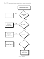
2.13 Personality Card Jumpers
WP (default: open): if closed, the EEPROM is write protected and the Save (SV) command
is disabled
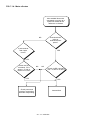
G1 (default: open) : if closed, connects TX- of serial link to 0V via pull-down resistor
G2
: if closed, gives priority to "opto" , if open gives priority to "keypad"
G3 (default: open) : if closed, set 9600 Baud rate and basic address 1
G4 (default: open) : if closed, connects TX+ of serial link to 5V via pull-up resistor
G5 (default: open) : if closed, connects a 120 Ω resistor between RX+ and RX- of serial link
CAUTION: it is recommended to close the WP jumper at the end of installation and
setup.
Fig. 2.15 - Personality Card
Jumper open
Jumper closed
2.13.1 G2 Jumper: "Keypad" or "Opto" Priority
The jumper G2 on the personality card gives priority to keypad or to opto to execute "Drive
Enable" command. " Drive Enable" opto isolated signals are connected to J8/ pos.13, 14, 15.
G2 open = keypad priority = the keypad (or the device connected to the serial link) is the
master, i.e. it allows to enable or disable motor current, whereas the optocouplers can only
disable (protection); they can enable after resetting only.
The "Drive Enable" and "Reference Enable" opto-isolated signals must be driven at +15V.
Such a procedure should be followed during installation and drive test.
G2 closed = opto priority = the optocouplers are the master and the keypad can only be
used for parameters setup.
Note:
1. See par.2.16.1 if the keypad does not communicate with the drive
2. "Drive Enable" priority is different from the use of the analog or digital reference.
You can choose an analog or digital reference by "AR" (Analog) or "DR" (Digital) commands,
and save. The drives are supplied set to digital reference "DR".
II - 33 - 30/Oct/01
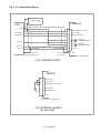
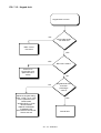
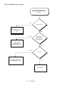
2.13.2 G1-G4-G5 Jumpers: Link Termination's
By default G1, G4 and G5 jumpers on the personality card are open (no link termination's on
modules). In fact, usually, it is not necessary to close G1, G4 and G5 jumpers because the
link termination's are already closed on the power supply; anyway, in specially noisy
environments, could be necessary to close them also, as follows.
• Environment without noise
To user
JP1,JP2,JP3
(see par.2.6)
G1,G4,G5
open
G1,G4,G5
open
G1,G4,G5
open
G1,G4,G5
open
Power
Supply
Module
Module
Module
Module
• Specially noisy environment
To user
JP1,JP2,JP3
(see par.2.6)
G1,G4,G5
open
G1,G4,G5
open
G1,G4,G5
open
G1,G4,G5
closed
Power
Supply
Module
Module
Module
Module
2.13.3 G3 Jumper: Basic Configuration
The jumper G3 on the personality card allows, if closed, to set 9600 Baud rate and basic
address 1. This configuration can be used to restore the communication in case of fault of
the serial link. When the communication has been restored, the G3 jumper must be open.
2.13.4 WP Jumper: Write Protection
The jumper WP on the personality card allows, if closed, to write protect the EEPROM. If
closed, the Save (SV) command is disabled.
CAUTION: it is recommended to close the WP jumper at the end of installation and
setup.
II - 34 - 30/Oct/01
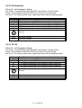
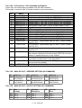
2.14 Potentiometer/Button
Tab. 2.30 - Potentiometer/Button
I LIMIT
POTENTIOMETER
RESET
BUTTON
Peak current control.
A full CCW rotation will set the current to zero.
A full CW rotation will set the current to 100%.
Digital control card reinitialization and reset
of protections.
2.15 Input/Output Characteristics
Tab. 2.31 - Input/Output Characteristics
OPTOISOLATED
INPUTS
Drive enable 1,2,3
Reference enable
Remote reset
OPTOISOLATED
OUTPUTS
Drive OK/ Motor OK
Analog tacho
outputs 1,2,3
Analog Out1
Analog Out2
Velocity differential
Reference Signals
1,2,3
Simulated Encoder
differential output
signals
z in =1.2 kΩ
I nom = 10 mA (8 to 20 mA)
Vmin = 15Vdc
Vmax = 25V
z out = 1.2 kΩ
I max = 20 mA
Vnom < 25 Vdc
z out = 100 Ω
I max = 5 mA
Range: see ET command
Gain error = ±10% over production spread
Max linearity error: ±2% over full range
z out = 100 Ω
I max = 10 mA
Full scale = ±10V
z in > 20 kΩ
Full scale = ±10V
z out = 100 Ω
Full scale = 7V (RS422/RS485 compatible)
II - 35 - 30/Oct/01
2.16 Serial Link Connection
REMARK: for the first installation it is strongly recommended to use either the
optional keypad or the DBTALK communication program.
2.16.1 Optional Keypad
The keypad is an optional accessory product which can be used for drive setup and
monitoring. The keypad must be connected to J10 connector of Power Supply.
If problems occur when attempting to communicate, the keypad is most likely set incorrectly.
To start the setup procedure press <CTRL>, then <CR>. For each parameter the current
setting is displayed, together with a question asking if you want to change it.
The correct setting is:
BAUD = 9600
WORD = 8D+E+1 STOP
BLOCK MODE
SINGLE LINE MODE
FLASHING OFF
KEY REPEAT ON SLOW
Be sure to save at the end of the procedure by pressing <Y> when the display shows: "Make
changes permanent Y/N".
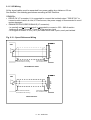
2.16.2 Connection to Personal Computer
2.16.2.1 RS232/RS485 Full-duplex Converter
The RS422 interface wiring is based on one-to-one, no multidrop, principle. Four wires are
used. With RS422, you can transmit and receive data simultaneously (full-duplex).
The RS485 half-duplex uses only two wires. It allows multidrop communication. With RS485
half-duplex, you cannot transmit and receive simultaneously.
We supports RS485 full-duplex with four wires (RS422 compatible). Up to 99 DBM and up to
15 DBS drives can be connected in multidrop configuration.
• RS232/485 CONVERTER KIT
This very small external converter provides a full-duplex interface between PC and DBM.
The converter must be fit directly into a COM port (RS232) of a PC. This way the link
becomes purely RS485, less susceptible to noise and able to transmit over much longer
distances than RS232.
The kit includes:
- the converter to fit into DB25-S connector of the PC (COM port)
The DTE/DCE switch of the converter must be set to DCE (Data Communications Equipment)
- a DB25 to DB9 interface (to be used if the PC COM port is DB9-S)
- a 2 m cable to connect the converter to DBM J10 connector
II - 36 - 30/Oct/01
• An optoisolated PC board RS 485 full-duplex driver can also be used. The following wiring
must be used.
RS485 full duplex
Connector
DBM J10 Connector
DBS J2 Connector
Male
Female
1 (+Rx)
2
3 (+Tx)
4-5
6 (-Rx)
7 (Gnd)
8 (-Tx)
9
(+Tx)
(-Tx)
(+Rx)
(-Rx)
(Gnd)
2.16.2.2 DBTALK Program
• PC REQUIREMENTS
- 80286, 80386, 80486 microprocessor or better
- Hard disk and one diskette drive. You need 2 Mbytes of disk space and 512 kbytes of RAM
- CGA, EGA, VGA, MCGA graphics card (color VGA recommended)
- MS-DOS 6.2 or later
- ANSI.SYS in CONFIG.SYS
• DBTALK PROGRAM
The DBTALK program is available on floppy disk
• INSTALL PROGRAM
- Insert diskette into drive A or drive B
- Type <a:install> (or <b:install>)
The installation program will create the Directory C:\DBTALK, will copy all the files in this new directory and will
start the program
• START PROGRAM (after the first installation)
- Type <cd dbtalk>
- Type <start>
• MOVE IN THE PROGRAM
Start the selected procedure
Select the field
Space
Reread parameters
Move up/down
Go to previous/next screen
Esc
Exit/Go to previous menu
II - 37 - 30/Oct/01
• SELECT PROGRAM
⇒ DBM linker
⇒ DBS linker
⇒ PDBS Linker (see PDBS Application Manual)
⇒ Setup
• SETUP to choose
⇒ Language: Italian or English
⇒ Serial link : COM1 or COM2
• UTILITY to
⇒ Scan Baud rates
⇒ Scan Faults
II - 38 - 30/Oct/01
⇒ Restore/store Personality Card parameters
To save the actual parameter set, select STORAGE PARAMETER, select the file (e.g. ST1), press <TAB> to
change the description and press <CR>
⇒ Set Baud rates
⇒ Start the Autophasing procedure
⇒ Set the "Adjustment of Torque/Speed curve" procedure
• MANUAL to
⇒ See/Reset Faults
If the fault condition is not present anymore, the fault will be reset automatically. To reset the fault on the
screen, go to the next screen with the arrow keys
II - 39 - 30/Oct/01
⇒ Display the Status
⇒ See/Change parameters
To change one parameter type the command string on the PC keyboard. Example: 3VE3000
II - 40 - 30/Oct/01
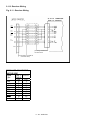
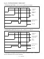
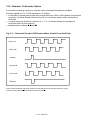
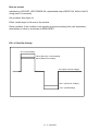
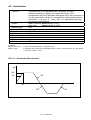
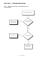
Fig.2.16 - STARTING SEQUENCE - TIMING CHART
1. PS-Standard and PS-6M: t1 = 8 to 10 s, t2 ≥ 1 s, t3 ≥ 20 ms, t4 = 3 s, t5 ≥ 0.5 s
t2
t1
t3
t4
t5
110/230 Vac
1-phase
400/460 Vac
3-phase
Drive
Enable
Remote Reset (*)
Motor OK
Drive OK
2. PS-Standalone and PS-120: t1 ≥ 20 ms, t2 ≥ 1 s, t3 ≥ 20 ms, t4 = 3 s, t5 ≥ 0.5 s
t1
t2
t3
t4
t5
400/460 Vac
3-phase
230 Vac 1-phase
(if applicable)
Drive
Enable
Remote Reset (*)
Motor OK
Drive OK
(*) CAUTION: the Remote Reset must be a single nonrepetitive signal. Otherwise it
must be filtered with 500 Hz cutoff frequency.
II - 41 - 30/Oct/01
3. PS-U: t1 = 6 s, t2 = 2 to 4 s, t3 = 4 s
WARNING: make sure that the AUX EXT CONTACT (pos.5 and 6 of J12 connector) is
connected to 24Vdc before starting.
t1
t2
t3
24 Vdc
400-460 Vac
3-phase
Drive
Enable
Motor OK
Drive OK
II - 42 - 30/Oct/01
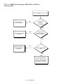
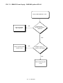
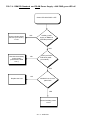
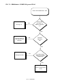
2.17 Starting Sequence
The starting sequence depends on the type of Power Supply. See Fig.2.16 for the Timing-chart.
∗ PS-Standalone and PS-120
1. Apply the 400Vac (or 460Vac) three phase power voltage
2. Apply (if applicable) the 230 Vac single phase auxiliary voltage via dedicated transformer
∗ PS-Standard and PS-6M
1. Apply the 230 Vac (or 110Vac) single phase auxiliary voltage
2. Apply the 400Vac (or 460Vac) three phase power voltage
∗ PS-U
1. Apply the 24 Vdc auxiliary voltage
2. Apply the 400Vac (or 460Vac) three phase power voltage
WARNING:
High Voltage - Discharge time approx. 6 minutes.
• Multimodule configuration only. Disconnect the first module from the serial link and assign
basic address to the second module and so on for the next modules (all the modules from
factory being usually configured with address 1,2,3 if triple-axis or with address 1,2 if doubleaxis).
Example of basic address assignment for the 2nd module, if the first module is triple-axis:
FROM KEYPAD
1 SA 4 <CR>
4 SV <CR>
Assign basic address 4 to the second module
Save the address configuration
Note: A module programmed as "address 4" will automatically assign for the other axes the
following addresses, i.e. 5 - 6 (if triple-axis) or 5 (if double-axis); and so on for the next basic
addresses.
• Check if NP (pole number), MV (max velocity), MR (max reference) and other required
parameters are OK for the application.
• Make a hardware reset via button on drive or via positive logic on pin 18 of J8 connector
(software reset via FA command being useless for digital control card reinitialization).
2.17.1 Autophasing
•
•
•
•
Check that the motor is free to rotate in both directions.
Check that no fault condition occurs (red drive-fault leds off).
The jumper G2 on the personality card must be open.
Check that all module axes have analog drive enable on via positive logic and digital drive
enable off.
• Send the password command for the module.
• Send the autophasing command for every axis of the module and save.
II - 43 - 30/Oct/01
Example for a double module with axis 4 and axis 5:
FROM KEYPAD
4 PW91 <CR>
PASSWORD ON
<CR>
4 AP <CR>
AUTOPHASING IN PROGRESS
AXIS PHASED
5 AP <CR>
AUTOPHASING IN PROGRESS
AXIS PHASED
4 SV <CR>
Give the password for the 2nd module
The correct answer is displayed
Only for optional keypad.
Allow axis 4 autophasing.
Allow axis 5 autophasing.
Save module 4 phasing.
• Repeat the password and autophasing procedures for subsequent modules (if applicable).
• Make a hardware reset via button on drive or via positive logic on pin 18 of J8 connector.
2.17.2 Wiring Check
Axes being phased it is possible to check the wiring by rotating the motor via its digital reference.
• Enable analog drive-enable and reference-enable via positive logic.
• Check that G2 is open for keypad priority.
• Send to every axis the ON command (to enable digital drive-enable) , the VE command (for
CW slow rotation), the VE- command (for CCW slow rotation), the OF command (to disable
the digital drive-enable).
Example of checking axis 5 rotation:
FROM KEYPAD
5 ON <CR>
{
5 VE 50 <CR>
5 VE-50 <CR>
5 OF <CR>
z
Enable digital drive-enable for axis 5
Drive enable led will be on
Set CW rotation at 50 rpm
Set CCW rotation at 50 rpm
Disable digital drive-enable for axis 5
Drive enable led will be off
2.17.3 CNC Priority
With CNC, the following procedures must be followed.
2.17.3.1 Setting Of Analog References
To set the modules to use the analog references from the CNC, it is necessary to enter the
password, to send the AR command to every axis and to save. ST command can be sent to
check if the commands have been accepted.
II - 44 - 30/Oct/01
Note that:
• AR command can be sent via global address (*).
• If there are two or more modules, PW (password) and SV (save) commands can be sent to
each module.
Example of enabling all the analog references for two modules with axes 1,2,3 and 4,5:
FROM KEYPAD
1 PW91 <CR>
PASSWORD ON
4 PW91 <CR>
PASSWORD ON
* AR <CR>
1 SV <CR>
4 SV <CR>
1 ST <CR>
A1 ST___ E___ I_0___
...
Give the password for the 1st module
The correct answer is displayed
Give the password for the 2nd module
The correct answer is displayed
Enable analog reference for all axes
Save the configuration for the 1st module
Save the configuration for the 2nd module
Ask the status for axis 1
Displays the axis 1 status. Check the 0 in the 2nd bit after I
Repeat ST command and check other axes
2.17.3.2 Drive Enable With CNC Priority
To give the priority for enabling and disabling the drive from the CNC, it is necessary to pull out
the personality card from the module, to solder G2 jumper and to pull in the card.
REMARK: if there are more than one module, do not swap the personality cards, this will swap
the module data.
When the above procedure is completed, the CNC is the master and the keypad is the slave, as
follows:
PARAMETERS MANAGED BY CNC:
drive enable, reference enable, speed references.
PARAMETERS MANAGED BY KEYPAD:
all dynamic parameters (acceleration,
deceleration, KI, KP, etc.), status and fault.
2.17.4 Velocity Offset
If it is necessary you can adjust the analog velocity offset by providing 0 analog speed
reference and setting VO command for an automatic adjustment. A fine adjustment can be
done with successive steps via OV command.
REMARK: the adjustment of the digital velocity offset must not be used to adjust the analog
velocity offset and it is reserved to setup technicians. It can be made by providing 0 digital
speed reference (VE=0) and setting OC command. The opto Drive Enable must be high.
II - 45 - 30/Oct/01
2.18 - Resolver To Encoder Option
For position sensing a resolver to encoder option (simulated encoder) is available.
Encoder signals are 7V, 100 Ω impedance, as follows:
• 2 channels of square wave output with a resolution from 128 to 16384 pulses per electrical
revolution. Channel B leads channel A by 90° for clockwise rotation when viewed from
shaft end.
• 1 marker pulse per electrical revolution (i.e. 1∗ 3 = 3 marker pulses per mechanical
revolution with a 6 pole resolver).
•. complementary outputs A, B and C.
Fig. 2.17 - Simulated Encoder (CW Rotation When Viewed From Shaft End)
Channel A
Channel B
C Marker
Channel A
Channel B
C Marker
Note: to make C Marker high when Channel A and Channel B are high (like Siemens), swap
Channel A with Channel A and Channel B with Channel B.
II - 46 - 30/Oct/01
2.18.1 Setup For Encoder Resolution
The number of pulses per electrical revolution of simulated encoder can be set via SE
software command.
Example of a setup for axis 1.
FROM KEYPAD
1 PW91 <CR>
PASSWORD ON
<CR>
1 SE 4096 <CR>
1 SE <CR>
A01 SIMULATED ENCODER = 4096
1 SV <CR>
Give the standard password for axis 1
The correct answer is displayed
Only for optional keypad
Set 4096 ppr to axis 1
Ask the number of ppr for axis 1
Save
REMARK: the maximum number of pulses per electrical revolution depends on the R/D
resolution. See the following Table.
The width of C marker can be A (360°), A/2 (180°) or A/4 (90°); it must be specified in the
order. This parameter does not depend on the software commands.
Note: to obtain the resolution per mechanical revolution it is necessary to multiply the pole
pairs by the electrical resolution.
Example: if a FAS T motor with 6 pole resolver is used, 1024 pulses per electrical revolution
mean 1024 ∗ 3 = 3072 pulses per mechanical revolution.
2.18.2 R/D Resolution
The resolution of Resolver to Digital converter will automatically be switched according to
actual speed for optimum system performance between minimum (see RN command in the
User's Manual) and maximum resolution (see RX command).
The speed range of R/D resolution is included in the following table.
Tab. 2.32 - Max speed and max ppr versus R/D resolution
Resolution (bit)
12
14
10
Max number of pulses per
electrical revolution
Max speed with 2 pole
resolver (rpm)
Max speed with 6 pole
resolver (rpm)
Max speed with 8 pole
resolver (rpm)
16
256
1024
4096
16384
24000
12000
3510
877
8000
4600
1170
292
6000
3510
877
219
II - 47 - 30/Oct/01
2.19 Mechanical Brake
FAS series servomotors have as option a 24 Vdc electromagnetic safety brake.
CAUTION: safety brake must be clamped and released with motor at standstill.
Premature failure of the brake will result if brake is used for dynamic stopping of the
motor.
The release of the brake (from 0V to +24V) and the clamp (from +24V to 0V) must follow the
sequence in Fig. 2.18.
FIG. 2.18 - BRAKING SEQUENCE, TIMING CHART
Note: T1 ≥ 200 ms, T2 = application dependent, T3 = 100 ms, T4 ≥ 200 ms
T1
OFF
T2
T3
T4
ON
DRIVE ENABLE
ON
OFF
BRAKE 24V
POWER SUPPLY
RELEASE
CLAMP
BRAKE
0V
REFERENCE
ENABLE
0 rpm
MOTOR SPEED
II - 48 - 30/Oct/01
2.20 Module Replacement
Once DBM module to be replaced has been identified, it is necessary to follow this procedure:
• Disconnect the power.
• Remove the Bus Bars (+HV, -HV and GND) and disconnect all connectors and flat cables.
• Unscrew the anchor screw on the top of the module and remove the module.
Remove the Personality Card, at the left of J1 connector, by loosening the two screws. After
removing the card, disconnect the flat cable.
REMARK: on the personality card a EEPROM is mounted. All dynamic parameters (dynamic
settings, autophasing, analog interfaces, ...) are stored in this EEPROM after every reset.
In case of module replacement, it is recommended to save all parameters with the save (SV)
command before removing the Personality Card ready for installation in the replacement
module. This retains and transfers all the previous module information's.
Remove the Personality Card from the new module and replace with the old one.
•
•
•
•
Mount the new module and tighten the anchor screw at the top.
Reassemble the Bus Bars, all the connectors and flat cables.
Check all connections.
Enable the auxiliary voltage and check by keypad or PC all application dependent parameters. In
particular: pole number, max velocity, max reference voltage, Ilimit, internal ramp generator.
II - 49 - 30/Oct/01
This page intentionally blank
II - 50 - 30/Oct/01
SECTION 3 - ELECTROMAGNETIC COMPATIBILITY (EMC)
3.1 European Directive (89/336/EEC)
Compliance with the European Directive 89/336/EEC is required for all electric and electronic
products brought onto the European market after December 31st, 1995.
DBM04 drives with FASTACT motors meet the following EMC product standard related to
the Directive:
EN 61800-3 (1996) and EN 61800-3/A11 (2000): "Adjustable speed electrical power drive
systems. Part 3: EMC product standard including specific test methods".
Second environment (industrial) compatibility levels.
Remark: equipments not intended to be used on a low-voltage public network which supplies
domestic premises. May cause radio frequency interference.
Tests have been made in an independent test house.
The installer of the drive is responsible for ensuring compliance with the EMC regulations
that apply where the drive is to be used. We recommend filtering as per par.3.2 and wiring,
grounding and screening as per par.3.3 and 3.4.
3.2 Filtering
The following filters are recommended.
3.2.1 Filter Types
Code
Trade-mark
AT6008
Schaffner
FN 250-6/07
Schaffner
FN 250-12/07
Schaffner
FN 258-7/07
Schaffner
FN 258-16/07
Schaffner
FN 258-30/07
Schaffner
FN 258-42/07
Schaffner
FN 258-55/07
Schaffner
FN 258-75/34
Schaffner
FN 258-100/35
AT6009
AT6010
AT6011
AT6012
AT6013
AT6014
AT6015
Rated Current
[A]
at 50°°C (40°°C)
(6)
Max Voltage
[Vac]
at 50°°C
250
(12)
250
7 (8.4)
3 x 480
16 (19.2)
3 x 480
30 (36)
3 x 480
42 (50.4)
3 x 480
55 (66)
3 x 480
75 (85)
3 x 480
100 (120)
3 x 480
III - 1 - 30/Oct/01
Drive type
DBM04 PS-Standard, PS-Standalone,
PS-6M, PS-120 (Aux Pwr)
DBM04 PS-U (Aux Pwr)
DBM04 PS Standard, PS-6M, PS-U and
PS-Standalone
DBM04 PS120
3.2.2 Filter Sizing
The filter/drive coupling in the previous table is a standard coupling. The filter can be
undersized according to the rms input current of the actual application. This should be done
not only because, as a matter of fact, undersizing the filter means less money, but because
the undersized filter provides better performance to EMC.
Example:
- DBM04 PS-Standard + DBM 04 6-6-6 + DBM 04 6-6-6 and contemporaneity factor of 0.8.
For this application it is not necessary to use the 55A filter of the table.
The reference current is Iin = 6 ∗ 6 ∗ 0.8 = 28.8 A
A 30A filter (FN 258-30/7) can safely be used.
3.2.3 Filter Dimensions
Code
Trade-mark
AT6008
Schaffner
FN 250-6/07*
Schaffner
FN 250-12/07*
Schaffner
FN 258-7/07
Schaffner
FN 258-16/07
Schaffner
FN 258-30/07
Schaffner
FN 258-42/07
Schaffner
FN 258-55/07
Schaffner
FN 258-75/34
Schaffner
FN 258-100/35
AT6009
AT6010
AT6011
AT6012
AT6013
AT6014
AT6015
L1
85
L2
75
L3
54
Dimensions
[mm]
L4
0
Weight
85
75
54
0
255
240
50
25
225±0.8 126±0.8
300
1.1
305
290
55
30
275±0.8 142±0.8
300
1.7
335
320
60
35
305
150
400
1.8
329
314
70
45
300
185
500
2.8
329
314
80
55
300
185
500
3.1
329
314
80
55
300
220
379±1.5
364
90±0.8
65
L5
65
L6
30
l7
300
[kg]
0.24
65
40
300
0.31
terminal
block
350±1.2 220±1.5 terminal
block
4
5.5
*= the FN250-6/07 and 12/07 filters have wiring leads (length=300mm) at both sides.
TOP VIEW
SIDE VIEW
L5
L1
L2
L6
L3
L4
III - 2 - 30/Oct/01
L7
3.2.4 Filter Installation
- The filter must be mounted on the same panel as the drive.
CAUTION: leave a clear space of at least 60mm around the filter for air circulation
when the cabinet does not have forced ventilation.
- The filter must be connected as close as possible to the drive input. If the separation
between filter and drive exceeds around 30 cm (1 ft.) then a flat cable should be used for
the RF connection between filter and drive
REMARK: when mounting the drive and the filter to the panel, it is essential that any paint or
other covering material be removed before mounting the drive and the filter.
- The maximum torque of mounting screws is as follows:
FILTER
FN 250 - 6/07
FN 250 - 12/07
FN 258 - 7/07
FN 258 - 16/07
FN 258 - 30/07
FN 258 - 42/07
FN 258 - 55/07
FN 258 - 75/34
FN 258 - 100/35
Max
torque
0.8 Nm
0.8 Nm
0.8 Nm
0.8 Nm
1.8 Nm
1.8 Nm
3.0 Nm
3.0 Nm
4.0 Nm
- The filter can produce high leakage currents (see Data Sheets by Schaffner)
- The capacitors within the filters have discharge resistors.
CAUTION: the filter must be connected to ground before connecting the supply
WARNING: High Voltage - Discharge time approx. 10 seconds
- The single phase filter can be installed on the left shoulder of the fan housing (Power
Supply side), as in the following figure:
To 220 Vac
(110 Vac)
main supply
To
AUX PWR
connector
III - 3 - 30/Oct/01
Fig. 3.2 - Grounding Of Shield To
Connectors At Motor Side
3.3 Wiring And Grounding
All the following cables must be shielded,
with 85% minimum shielding coverage:
- power motor cable (see Fig.3.1 and 3.2)
NOTES: if a power terminal board is used at motor
side, the shield must be RF connected to a metallic
PG gland.
- connectors at motor side can have a threaded
clamp. Cable shield must be grounded in the same
way as in Fig.3.2.
- resolver cable (see Fig.2.11 and Fig.3.2
motor side)
Fig. 3.1 - Grounding Of Shield To Motor
Connector At Drive Side
In case of Sub-D connector, cable shield
must be grounded to the metallic hood.
When there is not connector at drive side,
a kit with stand-off, screws and hose
clamps is provided.
The shield of the cable must be uncovered
from insulation coating and RF connected
to the stand-off through the hose clamp, as
in Fig.3.3.
Fig. 3.3 - Grounding Of Shield Without
Connector
- recovery resistor cable.
CAUTION: the recovery resistor cable
provided in kit is only for test purposes
and not EMC compliant.
- Reference, Enable and OK cable
- RS485 cable (flat cable between modules
excluded)
- simulated encoder cable (if applicable)
The shields of the cables must be
connected at both ends to the proper
housing via full circumferential bond to
metallic connectors or hose clamps.
III - 4 - 30/Oct/01
Fig. 3.4 - Cable Grounding At Drive Side
1 = Recovery resistor cable
2 = Reference, Enable, OK cable
3 = Motor power cable
Sub-D and unshielded cables not shown
III - 5 - 30/Oct/01
It is not necessary to shield the input power wires, the bus bars, the flat cables between the
modules.
REMARKs:
- the shields of cables inside the cabinet
must be 360° clamped to the cabinet wall
(see Fig. 3.5).
- "noisy" cables must be kept away from
"sensitive" cables by at least 30 cm (12 in).
Noisy cables include input-power wires,
motor power and brake wiring. Sensitive
cables include analog or digital signal
cables: resolver cable; reference, enable
and OK cable; RS485 serial link; simulated
encoder wiring.
- where noisy cables must cross power
cables, this must be done with angles as
near to 90° as possible.
Fig. 3.6 - Partition Penetration
Fig. 3.5 - Clamping To Cabinet
- the crossing of the cabinet should be
accomplished with a low impedance
connection between cable shield and
enclosure. If a connector is not involved,
the shortest practical lengths of connecting
strap should be used (see Fig.3.6).
Backpanel
(earth)
Enclosure
Strap
Cable Shield
Hex Head
Bolt
Screen is effectively
earthed 360° of its
radius
3.4 Recovery Resistor/ Motor Choke
To meet the EMC Directive, the ventilated enclosures containing dynamic braking resistors
must be conductive. The cable of recovery resistor must be shielded and the shield must be
360° clamped at both sides.
In some applications (e.g. some size 3 FAS T motors) a choke in series for each motor
phase has to be added. This choke must be shielded.
REMARK: when mounting the enclosure of recovery resistor or motor choke to the panel, it is
essential that any paint or other covering material be removed before mounting the enclosure
of recovery resistor or motor choke.
III - 6 - 30/Oct/01
3.5 Screening
To effectively screening the system all the single screens (CNC, electronic cabinet, machine,
motor housing, cables) must be connected together to effectively form one screen (see
Fig.1.4).
3.6 Safety Aspects
Noise suppression of Motor and Drive systems involves consideration of the earthing system,
and its effectiveness at high frequencies. It should not be forgotten that is the safety system
too and that the safety must take priority over EMC.
To reduce the radiated emissions, the use of capacitance to earth is very effective. In fact
DBM 04 drives have Y-type capacitors near the input power supply connector and Schaffner
filters also include them. These capacitors conduct current from phase to earth; this can be
in the order of hundreds of milliamperes.
WARNING: appropriate safety measures should be taken to ensure that this
potentially dangerous current flows to earth.
CAUTION: it is recommended to disconnect the drive and the EMC filters to carry out
the AC Voltage Tests of EN 60204-1 (1997), par.19.4, in order to not damage the Ytype capacitors between phases and ground. Moreover the DC voltage dielectric test
required by EN 50178 (1997), product family standard, has been carried out in factory
as a routine test. The DC Insulation Resistance Tests of EN 60204-1 (1997), par.19.3,
may be carried out without disconnecting the drive and the EMC filters.
III - 7 - 30/Oct/01
This page intentionally blank
III - 8 - 30/Oct/01
SECTION 4 - PROTECTIONS
4.1 Power Supply
Recovery not ok.
Indicated by: LED's DRF (drive fault) on all drives, LED DBR FAULT, optoisolated output
DRIVE OK, bit H of the FA string (see FA command).
Set condition: when recovery circuit or recovery resistor is broken, in short circuit; when the
recovery is active for too much time.
Effect: all drives inhibit torque
Reset condition: if the condition is not present anymore, power off and on monophase
voltage (PS-Standard and PS-6M) or 3-phase voltage (PS-Standalone, PS-120 and PS-U)).
Power supply overtemperature.
Indicated by: LED's DRF (drive fault) on all drives, LED OVER TEMP, optoisolated output
DRIVE OK, bit I of the FA string (see FA command).
Set condition: when a limit temperature is reached.
Effect: all drives inhibit torque.
Reset condition: if the condition is not present anymore, power off and on monophase
voltage (PS-Standard and PS-6M) or 3-phase voltage (PS-Standalone, PS-120 and PS-U).
IV - 1 - 30/Oct/01
4.2 Drive Module
Resolver not ok.
Indicated by: LED DRF, LED RF1/RF2/RF3 (Resolver Fault), optoisolated output DRIVE OK,
bit B of the FA string (see FA command).
Set condition: when the resolver is not connected or in short circuit at the power up, when the
resolver fails or is disconnected during running.
Effect: the drive inhibit torque of all axes of the module.
Reset condition: if the condition is not present anymore, reset button on drive or send pulse
to REM RESET.
Motor over temperature.
Indicated by: LED DRF, LED OT1/OT2/OT3, optoisolated outputs DRIVE OK and MOTOR
OK, bit C of the FA string (see FA command).
Set condition: when a limit temperature is reached inside the motor.
Effect: the drive inhibit torque of all axes of the module.
Reset condition: if the condition is not present anymore, reset button on drive or send pulse
to REM RESET.
Notes: the fault information via LEDS and opto is reset when the motor temperature goes
down the limit, while the drive is disabled until the reset condition has been met.
Power fault.
Indicated by: LED DRF, LED PWRF1/PWRF2/PWRF3, optoisolated output DRIVE OK, bit D
of the FA string (see FA command).
Set conditions:
1. When a short circuit is detected between motor phases, phase and ground, phase and
HV.
2. When overcurrent is detected in motor phases.
3. Overheating of power modules (locked rotor condition).
4. Undervoltage of internal supply of power modules
Effect: the drive inhibit torque.
Reset condition: if the condition is not present anymore, power off and on the power supply.
In case of condition 3. (overheating) wait at least 3 minutes before power up the drive.
IV - 2 - 30/Oct/01
Auxiliary voltages not normal
Indicated by: LED DRF, optoisolated output DRIVE OK
Set condition: when the level of +/- 15V or 5V becomes out of tolerance.
Effect: inhibit torque of all axes of the module.
Reset condition: if the condition is not present anymore, reset button on drive or send pulse
to REM RESET.
Personality card absent
Indicated by: LED DRF, optoisolated output DRIVE OK, bit L of the FA string .
Set condition: when the personality card is not present or taken away during running.
Effect: inhibit torque of all axes of the module.
Reset condition: if the condition is not present anymore, reset button on drive or send pulse
to REM RESET.
EEPROM error
Indicated by: LED DRF, optoisolated output DRIVE OK, bit L of the FA string (see FA
command), "EE ERROR" on the keyboard.
Set condition: when, after the SV command, a reset has been sent before 5 sec.
Effect: inhibit torque of all axes of the module.
Reset condition: check the parameters (e.g. KP, KI,..), correct the wrong values and save.
IV - 3 - 30/Oct/01
Bus not normal.
Indicated by: LED DRF, LED POWER OK, optoisolated output DRIVE OK, bit M of the FA
string (see FA command).
Set condition: See figure 4.1.
Effect: inhibit torque of all axes of the module .
Reset condition: if the condition is not present anymore at analog level (with hysteresis),
reset button on drive or send pulse to REM RESET.
FIG. 4.1 Bus Bar Voltage
810 V (overvoltage)
790 V (Recovery circuit enabled)
690 V (Reset max voltage)
540 V (Bus nominal voltage)
440 V (Reset min voltage)
410 V (Undervoltage)
IV - 4 - 30/Oct/01
Auxiliary HV referred voltages not norm.
Indicated by: LED DRF, optoisolated output DRIVE OK, bit N of the FA string (see FA
command).
Set condition: when the level of auxiliary voltages referred to power stage (-HV) becomes out
of tolerance.
Effect: inhibit torque of all axes of the module.
Reset condition: if the condition is not present anymore at analog level (with hysteresis) reset
button on drive or send pulse to REM RESET.
Overspeed
Indicated by: LED DRF, optoisolated output DRIVE OK, bit F of the FA string (see FA
command).
Set condition: when an error between set speed and actual speed bigger than the
programmed via EV command is detected.
Effect: inhibit torque on axis.
Reset condition: when the condition is no longer present, reset button on drive or send pulse
to REM RESET.
Drive overtemperature.
Indicated by: LED's DRF and DR.OVT, optoisolated output DRIVE OK, bit O of the FA string
(see FA command).
Set condition: when a limit temperature is reached on the heatsink.
Effect: inhibit torque of all axes of the module.
Reset condition: if the condition is not present anymore power off and on monophase
voltage.
Notes: the temperature limit is detected by thermo-switch.
IV - 5 - 30/Oct/01
IT
Indicated by: LED DRF, bit G of the FA string (see FA command).
Set condition: when the current exceeds the nominal motor current for a time longer than the
time stated by the motor thermal model (see IT command and Tab.6.6)
Effect: when the fault is going on the current limit is reduced to the level of the motor rated
current (set by PC command).
Reset condition: if the condition is not present anymore, the protection is reset. To reset the
fault status in FA string, push button on drive or send pulse to REM RESET.
Watchdog.
Indicated by: LED DRF, LED WTD, optoisolated output DRIVE OK.
Set condition: when the micro controller or DSP fails.
Effect: inhibit torque or all axes of the module.
Reset condition: if the condition is not present anymore reset button on drive or send pulse to
REM RESET.
IV - 6 - 30/Oct/01
SECTION 5 - ADJUSTMENT OF TORQUE/SPEED CURVE
In most of the DBM 04 applications, the magneto-motive force (MMF, that is, the stator
current vector) is perpendicular to the rotor flux. In such a way, the torque constant ( [Nm]
per Ampere) is maximized.
In some applications requiring extremely high speed and high frequency of the stator current,
the phase lag caused by the current controller imperfection might degrade the drive torque
constant. The current controller implemented within the DBM 04 drive results in a phase lag
of 9 degrees at the output frequency of 270 Hz.
Due to the phase lag, the spatial displacement between the rotor flux and the stator MMF will
be less than 90 degrees (electrical) and the torque will diminish as the cosine function of the
phase lag, and to optimize the Torque/Speed curve.
DBM 04 drive might compensate this phase lag and the lack of torque through the user
programmable phase advance. That is, an additional phase advance might be inserted into
the drive vector rotator, rendering the possibility to compensate for the current controller
phase lag.
Along with the conventional synchronous PM motors, the DBM 04 might run PM motors with
pronounced saliency effect (Ld ≠ Lq) and ensuring reluctance torque. The peak of total
electromagnetic torque for this family of PM motors is obtained with flux-MMF angles
different that 90 electrical degrees.
For the purpose of maximizing the torque per Amp constant of synchronous reluctance
motors, the phase advance in function of the speed and stator current is provided as a
standard feature of the DBM 04
5.1 Phase-speed relation
According to the requirements, the phase-speed curve equals zero for all the speeds below
the speed S1[rpm] (see Fig. 5.1). Above that speed, the phase rises with the speed with a
constant slope. Hence, two parameters (TF and TG in the following text) are sufficient for the
purpose of customizing the phase-speed demagnetization curve. TF parameter will define
the speed S1[rpm]. From the stall up to the S1[rpm], the phase(speed) correction will have
the value zero. Above S1[rpm], the phase(speed) correction will rise up with the constant
slope. This slope is defined by the second, TG parameter.
FIG. 5.1 - PHASE-SPEED CURVE
Phase (degrees)
S1[rpm]
= f(TF)
Slope = f(TG)
Speed [rpm]
V - 1 - 30/Oct/01
5.2 Phase-current relation
The phase-current curve is linearly rising or falling for the currents IQ>0, starting at the
current level S2[%] defined by the TY parameter, with a slope defined by TQ parameter.
FIG. 5.2 - PHASE-CURRENT CURVE
Phase (degrees)
S2[%] => TY
Slope=> TQ
Current IQ [%]
Hence, the point S2[%] is defined by TY parameter. According to requirements, the phasecurrent curve might increase at a steeper slope for the values of IQ superior to S2[%]. For
this purpose, the fourth, TQ parameter is provided in order to program the slope of the
phase-current curve for the values bigger than S2[%].
5.3 Parameters Setting for FAS T-V
To optimize the match between FAST-V brushless servomotors and DBM 04 drive, the
following parameters settings have been found to be the best choice. With these parameters
the motor provides, at the nominal speed and with nominal voltage - 5% (that is 380Vac for
400Vac-and 437Vac for 460Vac), a Max Torque from 1.5 to 3 times the Max Torque without the
optimization algorithm.
V - 2 - 30/Oct/01
Tab. 5.1 - Parameters Setting for 400V and 6-pole resolver
Motor type
FAS T0 V2 060
V4 060
V8 060
DBM 04
3/9
3/9
6/15
IL
100
100
100
TF
60
60
106
FAS T1 V2 030
V2 060
V4 030
V4 045
"
V6 030
"
V6 045
"
V8 030
"
V8 045
3/9
6/15
6/15
6/15
8/22
6/15
8/22
8/22
15/42
6/15
8/22
15/42
100
100
100
100
100
100
100
100
88
100
100
100
FAS T2 V2 030
V2 045
V4 020
V4 030
V6 020
V6 030
"
V8 020
"
V8 030
8/22
15/42
8/22
15/42
15/42
15/42
25/70
15/42
25/70
25/70
FAS T3 V2 020
V2 030
V3 020
V3 030
"
V4 020
V4 030
V6 012
V6 020
V8 012
V8 020
"
15/42
25/70
25/70
25/70
35/90
25/70
35/90
25/70
35/90
35/90
50/140
60/180
3
3
4
TY
115
87
127
TQ
19
26
21
38
106
58
88
58
58
42
92
60
60
48
60
8
4
7
5
5
7
7
6
5
7
7
4
94
127
166
133
89
127
87
127
66
97
66
74
22
21
30
22
25
21
19
21
28
14
16
23
100
100
100
100
100
100
73
100
65
100
32
60
30
36
32
54
54
32
30
52
6
5
9
7
12
8
9
8
7
7
51
102
76
74
69
66
40
102
61
102
22
26
17
17
15
14
22
16
27
16
100
100
100
100
100
100
100
100
100
100
100
77
30
42
28
54
46
36
52
22
30
20
30
30
7
7
8
9
9
9
7
15
12
16
10
10
140
135
122
79
61
94
76
112
0
76
0
0
23
21
20
15
15
19
17
19
9
14
10
13
V - 3 - 30/Oct/01
TG
Tab. 5.2 - Parameters Setting for 400V and 2-pole resolver
Motor type
FAS T0 C2 060
C4 060
C8 060
DBM 04
3/9
3/9
6/15
IL
100
100
100
TF
20
20
34
FAS T1 C2 030
C2 060
C4 030
C4 045
"
C6 030
"
C6 045
"
C8 030
"
C8 045
3/9
6/15
6/15
6/15
8/22
6/15
8/22
8/22
15/42
6/15
8/22
15/42
100
100
100
100
100
100
100
100
88
100
100
100
FAS T2 C2 030
C2 045
C4 020
C4 030
C6 020
C6 030
"
C8 020
"
C8 030
8/22
15/42
8/22
15/42
15/42
15/42
25/70
15/42
25/70
25/70
FAS T3 C2 020
C2 030
C3 020
C3 030
"
C4 020
C4 030
C6 012
C6 020
C8 012
C8 020
"
15/42
25/70
25/70
25/70
35/90
25/70
35/90
25/70
35/90
35/90
50/140
60/180
8
10
13
TY
115
87
127
TQ
19
26
21
12
34
18
28
18
18
14
30
20
20
16
20
23
13
20
16
14
20
21
19
16
22
22
13
94
127
166
133
89
127
87
127
66
97
66
74
22
21
30
22
25
21
19
21
28
14
16
23
100
100
100
100
100
100
73
100
65
100
10
20
10
12
10
18
18
10
10
16
18
16
26
20
37
23
26
25
22
21
51
102
76
74
69
66
40
102
61
102
22
26
17
17
15
14
22
16
27
16
100
100
100
100
100
100
100
100
100
100
100
77
10
14
8
14
18
12
16
6
10
6
10
10
22
21
25
26
27
28
21
45
36
49
30
30
140
135
122
79
61
94
76
112
0
76
0
0
23
21
20
15
15
19
17
19
9
14
10
13
V - 4 - 30/Oct/01
TG
Tab. 5.3 - Parameters Setting for 460V and 6-pole resolver
Motor type
FAS T0 V2 060
V4 060
V8 060
DBM 04
3/9
3/9
6/15
IL
100
100
100
TF
78
82
128
FAS T1 V2 030
V2 060
V4 030
"
V6 030
"
V6 045
"
V8 030
"
V8 045
3/9
6/15
6/15
8/22
6/15
8/22
8/22
15/42
6/15
8/22
15/42
100
100
100
100
100
100
100
88
100
100
100
FAS T2 V2 030
V2 045
V4 020
V4 030
V6 020
V6 030
"
V8 020
"
V8 030
8/22
15/42
8/22
15/42
15/42
15/42
25/70
15/42
25/70
25/70
FAS T3 V2 020
V2 030
V3 020
V3 030
"
V3 030+1.5mH
"+1.5mH
V4 020
V4 030
V4 030+1.5mH
V6 012
V6 020
V8 012
V8 020
"
V8 020+1.5mH
"+1.5mH
15/42
25/70
25/70
25/70
35/90
25/70
35/90
25/70
35/90
35/90
25/70
35/90
35/90
50/140
60/180
50/140
60/180
3
4
4
TY
163
140
204
TQ
29
31
35
48
128
76
92
76
58
116
70
76
60
86
8
4
7
7
7
7
8
6
7
7
5
145
204
245
158
238
161
230
120
245
166
151
26
35
88
31
50
30
35
33
53
24
27
100
100
100
100
100
100
73
100
65
100
54
88
46
60
38
72
66
52
52
76
9
6
7
7
11
7
7
9
11
7
143
174
197
166
166
222
133
235
140
225
24
44
43
30
24
65
50
62
64
53
100
100
100
100
100
100
100
100
100
100
100
100
100
100
77
100
77
48
76
48
76
60
46
38
50
76
54
30
42
26
46
46
26
26
9
13
12
9
9
9
8
11
11
11
15
12
12
10
10
12
12
230
225
217
225
174
143
110
225
230
133
243
148
207
189
145
112
87
56
59
47
77
28
24
24
59
71
22
22
18
29
32
40
20
25
V - 5 - 30/Oct/01
TG
Tab. 5.4 - Parameters Setting for 460V and 2-pole resolver
Motor type
FAS T0 C2 060
C4 060
C8 060
DBM 04
3/9
3/9
6/15
IL
100
100
100
TF
26
26
42
TG
10
12
12
TY
163
140
204
TQ
29
31
35
FAS T1 C2 030
C2 060
C4 030
C4 045
"
C6 030
"
C6 045
"
C8 030
"
C8 045
3/9
6/15
6/15
6/15
8/22
6/15
8/22
8/22
15/42
6/15
8/22
15/42
100
100
100
100
100
100
100
100
88
100
100
100
16
42
24
28
30
24
18
38
22
24
20
28
24
12
22
16
21
22
22
24
18
22
20
16
145
204
245
235
158
238
161
230
120
245
166
151
26
35
88
44
31
50
30
35
33
53
24
27
FAS T2 C2 030
C2 045
C4 020
C4 030
C6 020
C6 030
"
C8 020
"
C8 030
8/22
15/42
8/22
15/42
15/42
15/42
25/70
15/42
25/70
25/70
100
100
100
100
100
100
73
100
65
100
18
28
14
20
12
24
22
16
16
24
28
18
22
22
32
22
21
26
33
20
143
174
197
166
166
222
133
235
140
225
24
44
43
30
24
65
50
62
64
53
FAS T3 C2 020
C2 030
C3 020
C3 030
"
C3 030+1.5mH
"+1.5mH
C4 020
C4 030
C4 030+1.5mH
C6 012
C6 020
C8 012
C8 020
"
C8 020+1.5mH
"+1.5mH
15/42
25/70
25/70
25/70
35/90
25/70
35/90
25/70
35/90
35/90
25/70
35/90
35/90
50/140
60/180
50/140
60/180
100
100
100
100
100
100
100
100
100
100
100
100
100
100
77
100
77
16
24
16
20
24
14
12
16
24
18
10
14
8
14
14
8
8
28
40
36
28
27
26
25
32
33
32
44
37
37
29
29
35
35
230
225
217
225
174
143
110
225
230
133
243
148
207
189
145
112
87
56
59
47
77
28
24
24
59
71
22
22
18
29
32
40
20
25
V - 6 - 30/Oct/01
SECTION 6 - COMMANDS
6.1 General Features
For serial communication, according to standard RS485, DBM drives are connected in
parallel (multidrop) and in "slave" configuration, whereas the CNC, the PC or the keypad are
in "master" configuration.
This is because the protocol is configured so that the drives are able to communicate only if
inquired by the master, to avoid contentions on the line. As a consequence, all the
commands have been configured individually (single axis questioned), except those for
which an answer is not foreseen; therefore all the drives can be reached simultaneously.
There are 3 kinds of command:
• status monitoring
Monitor commands on the status of the drive, which displays axis configuration and eventual
faults.
• data monitoring
Monitor commands for displaying memorized motion parameters (e.g. I limit=100%, etc.).
• data (command) input
Execute commands for setting and changing parameters (e.g. speed, pole number,
acceleration, deceleration, etc.).
Remark: if a mistake has been made while digitizing, it is possible to reset the command by
pressing <CR> ( <CARRIAGE RETURN> ).
The commands are in ASCII format:
1 bit-start
8 bit-data
1 bit-parity even
1 bit-stop
Serial communication speed can vary from 1200 to 19200 Baud.
VI - 1 - 30/Oct/01
Command syntax is as follows:
status monitoring:
data monitoring:
data input:
command input:
address COMMAND
address COMMAND
address COMMAND data
address COMMAND
Remark: press <CR> after each command string if the optional keypad is used.
• Address: there are three kinds of address:
Axis: it is a number from 1 to 9 ( max. number of axes in a system); it identifies the axis
selected for data monitoring / input.
Module: the "module" (or "basic") address is referred to the possibility to get the execution of
the command either addressing the chosen axis (axis) or any axis inside the module
(
module ). This last possibility is valid for all axes within a module common commands (e.g.
temperature).
Global: it is also possible to globally address all axes (global address) using the <∗> in place
of the address number.
• Command: it consists of two letters (e.g. AC, AE, etc.).
• Datum: it can be composed by a max. of 4 figures or 3 figures and the <-> symbol. The
<+> symbol is optional. Any data without a symbol is considered as positive.
VI - 2 - 30/Oct/01
6.2 Commands
All commands available for system management can be used to monitor and execute every
datum.
To monitor, it is sufficient to enter the address and the command; to execute, the address,
the command and the datum must be typed.
Tab. 6.1 List of Commands
Symbol
Command
Symbol
Command
AC
AD
AE
AL
AP
AR
AS
BR
CG
CP
CU
CV
DE
DF
Acceleration
Axis disabled
Axis enabled
Analog limit
Autophasing
Analog reference
Address show
Baud rate
Current gain
Current position
Current U offset
Current V offset
Deceleration
Digital velocity
reference filter
Direction
Digital limit
Digital reference
Extra parameter for
spare output
Extra parameter for
Tacho output
Error velocity
Fault
I Limit
IT protection
Integral gain
Proportional gain
Max reference
Max velocity
Number of poles
Velocity Fine offset
OF
ON
OV
PC
PR
Off
On
Offset Display
Peak current
Motor poles to resolver
poles ratio
Password
A/D resolution
Minimum of R/D
resolution
Resolver shaft
Maximum of R/D
resolution
Set Address
Simulated encoder
Spare output
Show Release
Status
Save
Torque Control
T/S adjustment (1/4)
T/S adjustment (2/4)
T/S adjustment (3/4)
T/S adjustment (4/4)
Velocity Control
Velocity
Velocity Offset
Velocity structure
DI
DL
DR
ES
ET
EV
FA
IL
IT
KI
KP
MR
MV
NP
OC
PW
RE
RN
RS
RX
SA
SE
SO
SR
ST
SV
TC
TF
TG
TQ
TY
VC
VE
VO
VS
VI - 3 - 30/Oct/01
Tab. 6.2 - Standard/Default Configuration
Standard
AC
AL
AR
BR
CG
CU
CV
DE
DF
DL
DR
ES
ET
EV
IL
IT
KI
KP
MR
MV
NP
OC
OV
PC
PR
RN
RX
RS
SA
SE
TC
TF
TG
TQ
TY
VC
VO
VS
1
address
2
address
3
address
4
address
5
address
0
DL
DR
9600
2
0
0
DL
DR
16
80
0
100
see Tab.6.6
10
20
100
128
see Tab.6.6
1
VC
see Sect.V
see Sect.V
see Sect.V
see Sect.V
VC
128
1
Note: with G3 jumper on the personality card closed, BR=9600 and SA=1 are set.
VI - 4 - 30/Oct/01
6
address
AC - Acceleration
Function:
Syntax:
Address type:
Unit of measure:
Range:
Default:
Password:
(∗) addressing:
Opposite to:
See also:
Examples:
1 AC 100 <CR>:
2 AC <CR>:
it allows to set an acceleration ramp. Whatever the input
reference (analog or digital), the system will follow it, but
accelerations will never be faster than those set by this command. It
can be useful when the drive is connected to rather simple position
controllers ( e.g. max, 0, -max), with an application requiring
progressive accelerations.
data monitoring: address AC <CR>
data input:
address AC n <CR>
axis
n = ms
10 to 999 or 0
0 (disabled)
no
yes
DE
it sets an acceleration ramp = 100ms for axis1.
it questions axis 2 about the acceleration ramp. In case no one has been set, the answer
is: "A2 ACC. TIME = ms 0".
FIG. 6.1 - Acceleration/Deceleration
rpm
MV
DE
VE
ms
AC
DE
AC
VI - 5 - 30/Oct/01
AD - Axis Disabled
Function:
Syntax:
Address type:
Unit of measure:
Range:
Default:
Password:
(∗) addressing:
Opposite to:
See also:
AD command makes the logic section ignore an axis and the
relatives faults. It is useful with DBM 2-axis: if the
third axis were not disabled, the logic would reveal resolver
fault and motor overtemperature, preventing the drive from
running.
data monitoring: address AD <CR>
data input:
address AD n <CR>
axis
n = axis number
1 to 99
yes
no
AE
AE
Note: the axis disabled holds his address, which can be interrogated via FA command.
REMARK: AD and AE commands must be set only when the motor is standstill
Examples:
1 AD 3 <CR>:
4 AD 6 <CR>:
1 AD <CR>:
it disables the 3rd axis of a module, whose first address is 1.
it disables the 3rd axis of a module, whose first address is 4.
"1 AXIS DISABLED 3" will be displayed if the 3rd axis is disabled. "1 AXIS DISABLED 1 3"
will be displayed if the 1st and 3rd axis is disabled.
AE - Axis Enabled
Function:
Syntax:
Address type:
Unit of measure:
Range:
Default:
Password:
(∗) addressing:
Opposite to:
See also:
Examples:
1 AE 3 <CR>:
4 AE 6 <CR>:
1 AE <CR>:
the AE command enables an axis and relative faults.
data monitoring: address AE <CR>
data input:
address AE n <CR>
axis
n = axis number
1 to 99
yes
no
AD
AD
it enables the 3rd axis of a module, whose first address is 1.
it enables the 3rd axis of a module, whose first address is 4.
"1 AXIS ENABLED 3" will be displayed if the 3rd axis is enabled. "1 AXIS ENABLED 1 3"
will be displayed if the 1st and 3rd axis is enabled.
VI - 6 - 30/Oct/01
AL - Analog Limit
Function:
Syntax:
Address type:
Unit of measure:
Range:
Default:
Password:
(∗) addressing:
Opposite to:
See also:
Examples:
1 AL <CR>:
it informs the controller that I limit reference to be considered is
analog (see J7 connector).
command input: address AL <CR>
axis
digital I Limit
yes
yes
DL
DL, IL, ST
Sets the analog I limit for axis 1. The display is cleared. After this command a current
limit can be set via J7 connector, pos. 12, 13 and 14 (range 0 to 10V).
The status can be interrogated via ST command.
REMARK: DBM 04 has the "Analog I limit" as standard.
AP - Autophasing
Function:
Syntax:
Address type:
Unit of measure:
Range:
Default:
Password:
(∗) addressing:
Opposite to:
See also:
AP command allows resolver auto-phasing. As in this phase the
motor can rotate for a revolution fraction, it is opportune to make
sure it is free to rotate to avoid risk of friction, which could
compromise phasing accuracy. So, motor must be disconnected
from load.
command input:
address AP <CR>
axis
non-phased axes
yes
no
ON, OF
Note: To execute AP, all module axes must have optoisolated Drive Enable signals "on" and digital ones "off"
(see paragraph 2.2.3) via OF command. To execute AP, it is necessary that the "G2" jumper on the
personality card is open, which means priority from the keypad (see paragraph 2.2.2.).
Examples:
1 AP <CR>: it allows axis 1 auto-phasing. During such operation (a few seconds) "AUTOPHASING IN
PROGRESS" will be displayed; when auto-phasing is successfully carried out "AXIS PHASED" will be
displayed, otherwise "ERROR IN AUTOPHASING" will be shown. If digital Drive Enable is enabled (ON) (see
above) the message "WARNING DRIVE EN. CLOSED" will appear. The auto-phasing is not allowed if a
fault is on. This case, the message displayed will be "ERROR: FAULT STATUS".
VI - 7 - 30/Oct/01
AR - Analog Reference
Function:
Syntax:
Address type:
Unit of measure:
Range:
Default:
Password:
(∗) addressing:
Opposite to:
See also:
AR command allows enabling analog (speed or torque) reference.
The drive will follow as reference the voltage of connector J7
pins, ignoring VE command given from keypad.
command input:
address AR <CR>
axis
digital reference
yes
yes
DR
DR
Note: the status can be interrogated via ST command (bit I).
AS - Address Show
Function:
Syntax:
Address type:
Unit of measure:
Range:
Default:
Password:
(∗) addressing:
Opposite to:
See also:
Examples:
∗ AS <CR>:
it allows display of the basic address of a module, if unknown. To
avoid simultaneous answers on the line from more than one
module, it is necessary that serial flat J2 is connected only between
power supply and the questioned module. It is different from
SA command, which is used to change basic address.
data monitoring: ∗ AS <CR>
no
compulsory
SA
if the "base" address for such a module is 1, the answer will be "ADDRESS MODULE 1".
VI - 8 - 30/Oct/01
BR - Baud Rate
Function:
Syntax:
Address type:
Unit of measure:
Range:
Default:
Password:
(∗) addressing:
Opposite to:
See also:
Note:
it allows to change transmission speed of the serial link.
data monitoring: address BR <CR>
data input:
address BR n <CR>
module
n = Baud
1200, 2400, 4800, 9600, 19200
9600
yes
yes
-
To modify the Baud Rate also at keypad side, it is necessary to type <Control> and after <CR>.
Type <Y> to change Baud Rate and after <CR>.
CG - Current Gain
Function:
Syntax:
Address type:
Unit of measure:
Range:
Unit of measure:
Default:
Password:
(∗) addressing:
Opposite to:
See also:
The current loop gain of the DBM drive might be adjusted through
the serial link communication. A dedicated CG parameter with
4 discrete values is introduced in order to set the current error gain.
data monitoring: address CG <CR>
data input:
address CG n <CR>
axis
0=very low gain
1=medium low
2=medium high
3=very high
2
YES
no
-
VI - 9 - 30/Oct/01
CP - Current Position
Function:
Syntax:
Address type:
Unit of measure:
Range:
Default:
Password:
(∗) addressing:
Opposite to:
See also:
Examples:
2 CP <CR>:
it allows to know the position relative to electric revolution of the
resolver at start-up. It is used when the application requires to
know the absolute position.
data monitoring: address CP <CR>
axis
0 to 4096
no
no
-
Interrogates axis 2 about the current position. If the starting position is 4006, the
answer will be : "A02 CURRENT POSITION = 4006".
CU - Current U offset (only for setup technicians)
Function:
Syntax:
Address type:
Unit of measure:
Range:
Default:
Password:
(∗) addressing:
Opposite to:
See also:
it allows to set the offset of U phase current
data monitoring: address CU <CR>
data input:
address CU n <CR>
axis
0 to 255
no
no
CV
Note: the CU command must be executed with digital Drive Enable disabled (via OF command) and the opto
Drive Enable enabled.
Examples:
2 CU <CR>:
Interrogates axis 2 about the offset of the U current. If U current offset is 128, the
answer will be : "A02 CURRENT U OFFSET = 128".
CAUTION: do not change CU parameter. A wrong set of CU increases torque ripple.
VI - 10 - 30/Oct/01
CV - Current V offset (only for setup technicians)
Function:
Syntax:
Address type:
Unit of measure:
Range:
Default:
Password:
(∗) addressing:
Opposite to:
See also:
it allows to set the offset of V phase current
data monitoring: address CV <CR>
data input:
address CV n <CR>
axis
0 to 255
no
no
CU
Note: the CV command must be executed with digital Drive Enable disabled (via OF command) and the opto
Drive Enable enabled.
Examples:
1 CV <CR>:
Interrogates axis 1 about the offset of the V current. If V current offset is 128, the
answer will be : "A01 CURRENT V OFFSET = 128".
CAUTION: do not change CV parameter. A wrong set of CU increases torque ripple.
DE - Deceleration
Function:
Syntax:
Address type:
Unit of measure:
Range:
Default:
Password:
(∗) addressing:
Opposite to:
See also:
Examples:
1 DE 100 <CR>:
1 DE <CR>:
it allows to set a deceleration ramp. Whatever the input reference
(analog or digital), the system will follow it, but decelerations will
never be faster than those set by this command. It can be
useful when the drive is connected to a rather simple position
controller (e.g. max,0,-max), with an application requiring
progressive decelerations (see Fig. 6.1).
data monitoring: address DE <CR>
data input:
address DE n <CR>
axis
n = ms
10 to 999 or 0
0 (disabled)
no
yes
AC
it sets a deceleration ramp = 100 ms for axis 1.
it questions axis 1 about the deceleration ramp. In case no one has been set, the
answer is: "A01 DECEL. TIME = ms 0"
VI - 11 - 30/Oct/01
DF - Digital Filter
Function:
Syntax:
Address type:
Unit of measure:
Range:
Default:
Password:
(∗) addressing:
Opposite to:
See also:
it allows to set a low-pass digital filter. The filter reduces high
frequency noise and resonance's
When the Velocity Structure command is VS=0 or VS=1, the
velocity reference is filtered.
When the Velocity Structure command is VS=2 or VS=3, the
velocity error is filtered.
The value DF=0 switches the filter OFF
data monitoring: address DF <CR>
data input:
address DF n <CR>
axis
0 to 255. The filter bandwidth is:
f [Hz] = {ln[1/(1-DF/512)]}/(2π∗300 10-6)
0 (disabled)
yes
no
VS
Note: the DF command must be executed with digital Drive Enable disabled (via OF command) and the opto
Drive Enable enabled.
Examples:
2 DF 165 <CR>:
2 DF <CR>:
sets the filter bandwidth to 206 Hz for axis 2.
Interrogates axis 2 about the reference filter on the velocity reference. The answer will be
: "A02 DIG.FIL. REF. PAR. = 165".
Tab. 6.3 - Filter Bandwidth
DF Frequency DF Frequency DF Frequency DF Frequency
1
1 Hz
65
72 Hz
130
155 Hz
195
254 Hz
5
5 Hz
70
77 Hz
135
162 Hz
200
262 Hz
10
10 Hz
75
84 Hz
140
169 Hz
205
271 Hz
15
15 Hz
80
90 Hz
145
176 Hz
210
280 Hz
20
21 Hz
85
96 Hz
150
183 Hz
215
288 Hz
25
26 Hz
90
102 Hz
155
191 Hz
220
297 Hz
30
32 Hz
95
108 Hz
160
198 Hz
225
307 Hz
35
37 Hz
100
115 Hz
165
206 Hz
230
316 Hz
40
43 Hz
105
121 Hz
170
214 Hz
235
325 Hz
45
48 Hz
110
128 Hz
175
221 Hz
240
335 Hz
50
54 Hz
115
134 Hz
180
229 Hz
245
345 Hz
55
60 Hz
120
141 Hz
185
237 Hz
250
355 Hz
60
66 Hz
125
148 Hz
190
246 Hz
255
366 Hz
VI - 12 - 30/Oct/01
DI - Direction
Function:
Syntax:
Address type:
Unit of measure:
Range:
Default:
Password:
(∗) addressing:
Opposite to:
See also:
Example:
4 DI <CR>:
it allows to invert the direction of the motor rotation, in case of
analog or digital reference. The drive is supplied set to CW
rotation, (viewed from shaft end) corresponding to positive
during the installation. To know what the actual configuration is,
ST command shall be asked.
command input:
address DI <CR>
axis
CW
no
yes
ST
it reverses the direction of motor rotation for axis 4. The display is cleared.
Note: The status can be interrogated via ST command (bit L).
DL - Digital Limit
Function:
Syntax:
Address type:
Unit of measure:
Range:
Default:
Password:
(∗) addressing:
Opposite to:
See also:
it informs the controller that the I limit reference to be considered as
active is digital (programmable via IL command).
command input:
address DL <CR>
axis
digital I limit
yes
yes
AL
AL, IL
Note: the status can be interrogated via ST command (bit J).
VI - 13 - 30/Oct/01
DR - Digital Reference
Function:
Syntax:
Address type:
Unit of measure:
Range:
Default:
Password:
(∗) addressing:
Opposite to:
See also:
it allows to enable digital (speed or torque) reference. The drive
will consider as reference the number set via VE command and
ignore connector J7 voltage.
command input:
address DR <CR>
axis
digital reference
yes
yes
AR
AR
Note: the status can be interrogated via ST command (bit I)
ES - Extra parameter for Spare output
Function:
Syntax:
Address type:
Unit of measure:
Range:
Default:
Password:
(∗) addressing:
Opposite to:
See also:
Examples:
1 SO 1 <CR>:
1 ES 16 <CR>:
1 ES 32 <CR>:
1 ES 8 <CR>:
8 SO 5 <CR>:
2 ES 16 <CR>:
it allows to scale the Analog Outputs (max current, speed reference
or error reference) on J8 connector.
data monitoring: address ES <CR>
data input:
address ES n <CR>
1=Analog Output 1 (see J8 connector, pos.4)
2=Analog Output 2 (see J8 connector, pos.5)
0 to 255. Analog outputs on J8 connector (±10V, 10 mA max):
Max current for axis 1 (SO=1), axis 2 (SO=2) or axis 3 (SO=3):
±(10∗ES/16)V for ±100% max current
Speed reference for axis 1 (SO=4), axis 2 (SO=5) or axis 3 (SO=6),
and velocity error for axis 1 (SO=7), axis 2 (SO=8) or axis 3 (SO=9):
±[(ES∗NP∗MV)/(786∗MR)]V for ±MV (max velocity)
16
yes
no
MR, MV, NP, SO, Tab.6.4, Tab.6.5
sets analog out1 (J8 conn., pos.4) to max current of axis 1 of the first module
sets analog out1 to ±10V for ±100% max current of axis 1
sets analog out1 to ±10V for ±50% max current (zoom-in) of axis 1
sets analog out1 to ±5V for ±100% max current (zoom-out) of axis 1
sets analog out2 (J8 conn., pos.5) to speed reference of axis 2 of the third module
sets analog out2 to ±10V for ±6140 rpm (if NP=8 and MR=100 have been set for axis 2)
VI - 14 - 30/Oct/01
Tab. 6.4 - ES for Max Current (SO=1 to SO=3)
ES
MAX
ANALOG
CURRENT
OUT
8
100 %
5V
16
100 %
10 V
32
50 %
10 V
REMARK
actual current
The voltage at the Analog Output
represents the envelope of the actual
current.
Analog Output (envelope)
1. To calculate the max current, Imax:
- check the max current of the drive (see the rating plate or par.1.3).
- search for the max Analog Out voltage during the entire duty cycle.
- % scale according to ES, and Tab.6.4
2. To calculate the max rms current, Imrms =
Imax
:
2
3. To calculate the rms current:
- calculate the max rms current for each step of the duty cycle (acceleration, deceleration, ...)
- use the following formula
Imrms1 2 ∗ t 1 + Imrms2 2 ∗ t 2 + ...
t 1 + t 2 + ...
Irms =
SPECIAL CASES
Imax
2
Sinusoidal Analog Output: Irms =
2
=
Imax
2
Imax
Triangular Analog Output (I Limit): Irms =
2
3
=
Imax
2.45
Tab. 6.5 - ES for Speed Reference and Velocity Error (MR=100, SO=4 to SO=9)
2 pole resolver
ES
52
65
105
131
MV ANALOG
rpm
OUT
6046
8V
6046
10 V
2994
8V
3000
10 V
6 pole resolver
ES
17
22
35
44
52
65
MV
rpm
6165
5954
2994
2977
2015
2015
8 pole resolver
ANALOG
OUT
8V
10 V
8V
10 V
8V
10 V
VI - 15 - 30/Oct/01
ES
13
16
26
33
39
49
MV
rpm
6046
6140
3023
2977
2015
2005
ANALOG
OUT
8V
10 V
8V
10 V
8V
10 V
ET - Extra parameter for Tacho output
Function:
Syntax:
Address type:
Unit of measure:
Range:
Default:
Password:
(∗) addressing:
Opposite to:
See also:
it allows to scale the Tacho Tests outputs on J8 connector
data monitoring: address ET <CR>
data input:
address ET n <CR>
axis
50 to 100. Tacho outputs = ±(ET/10) ∗ (MR/100) [V] for ±MV
80
yes
no
MR, MV
Examples:
1 MV 3000 <CR>: sets max velocity to 3000 rpm for axis 1.
1 MR 100 <CR>: sets max velocity reference to 10 V for axis 1.
1 ET 50 <CR>:
sets ET parameter to 50 for axis 1. The Tacho Test 1 (J8, pos.1) will be ± 5V for
± 3000 rpm.
1 ET <CR>:
questions axis 1 about the extra parameter for Tacho Test 1. The answer is: "A01 EXTRA
PAR. FOR TO = 50".
EV - Error Velocity
Function:
Syntax:
Address type:
Unit of measure:
Range:
Default:
Password:
(∗) addressing:
Opposite to:
See also:
Remark:
it allows to set the maximum velocity error between reference
velocity and the actual speed in rpm. If the set value is overcome,
a fault occurs. Value = 0 disables the command.
data monitoring: address EV <CR>
data input:
address EV n <CR>
axis
n = rpm
1 to MV. 0 = disabled
0
yes
no
-
While testing the drives via step response, it is advisable to disable this protection or set a
high value of tolerated error, to avoid continuous faults.
Examples:
1 EV 100 <CR>:
1 EV <CR>:
it sets axis 1 to tolerate up to 100 rpm error, without fault.
it questions axis 1 about the maximum error allowed. The answer is: "A1 VELOCITY
ERROR RPM = 100".
VI - 16 - 30/Oct/01
FA - Fault
Function:
as only main faults have front panel LED indications, when the
generic LED DRF lights up, it is necessary to interrogate
the drive via FA command. The answer is a codified ASCII string
(see below). Another function of the command is to reset the faults
occurred at logic level (also resettable via push button).
status monitoring and reset: address FA <CR>
axis
no
no
Syntax:
Address type:
Password:
(∗) addressing:
Answer explanation: A a FA b c d e f g P h i j k l MA m n o B p q r
A
a
= axis
= axis address
FA
b
c
d
e
f
g
= fault
= Resolver connection
= Motor temperature
= Axis short circuit
= Bus Bar voltage (Axis 3 only)
= Velocity error
= It
P
h
i
j
k
l
= Power supply
= Recovery unit
= PWRS temperature
= n.c.
= n.c.
= Personality card
MA
m
n
o
= A module (DBM module)
= BUS BAR voltage
= Aux. Volt. ref. to - HV
= A module temperature
B
p
q
r
0 = OK
0 = OK
0 = OK
0 = OK
0 = OK
0 = off
1 = not OK
1 = overtemperature
1 = short circuit
1 = under 430V
1 = not OK
1 = on
0 = OK
0 = OK
1 = not OK
1 = overtemperature
0 = OK
1 = not OK*
0 = OK
0 = OK
0 = OK
1 = overvoltage/undervoltage
1 = out of tolerance
1 = overtemperature
= B module (eventual expansion module)
= BUS BAR voltage
0 = OK
= Aux. Volt. ref. to - HV
0 = OK
= B module temperature
0 = OK
1 = overvoltage/undervoltage
1 = out of tolerance
1 = overtemperature
* = in case of checksum error, check the parameters (e.g. KP, KI,...), correct the wrong values and save.
Note: If the expansion missing, the last characters are not significant.
Examples:
1 FA <CR>:
if OK, the answer will be: "A1 FA 000000 P 00000 MA 000 B 000"
VI - 17 - 30/Oct/01
IL - I Limit (Current Limit)
Function:
Syntax:
Address type:
Unit of measure:
Range:
Default:
Password:
(∗) addressing:
Opposite to:
See also:
it allows to program the peak current. It is useful when
undersized motors are used or during special tests.
data monitoring: address IL <CR>
data input:
address IL n <CR>
axis
n = % max current
0 to 100
100
no
no
DL, AL
REMARK: before executing IL command it is necessary to perform DL command.
Examples:
2 IL <CR>:
2 IL 90 <CR>:
it asks axis 2 about I limit. In default case the answer will be: "A2 CURRENT LIMIT % =
100".
it sets 90% current limit for axis 2.
IT - IT Protection
Function:
Syntax:
Address type:
Unit of measure:
Range:
Default:
Password:
(∗) addressing:
Opposite to:
See also:
Notes:
it allows to manage the IT thermal protections which prevents the
motor from an overheating too quick for the PTC operating
time. When the integral of current multiplied by time exceeds the
IT value, drive limits, after operating time, to nominal motor
current (see Tab. 6.6).
data monitoring: address IT <CR>
data input:
address IT xx n <CR>. xx = special password
axis
n = ms
0 to 255. 0 = protection disabled
see Tab. 6.6
special password
no
PC
IT status can be interrogated via FA command (bit g).
CAUTION: do not change IT parameter. A wrong set of IT can damage the motor.
VI - 18 - 30/Oct/01
Tab. 6.6 - IT Protection
The following table shows IT and PC values set in factory.
MOTOR
In (A)
In (A)
Ip (A)
IT
PC
IL
Operating
time at
drive peak
current
(s)
FAS K0V 020 060
2.9
8
22
12
18
100
4.9
FAS K1V 080 030
5.3
15
42
2
17
100
26.2
FAS T0 V2 060
1.1
3
9
9
17
100
5.8
FAS T0 V4 060
1.5
3
9
8
23
100
12.1
FAS T0 V8 060
3
6
15
8
28
100
18.2
FAS T1 V2 030
1.7
3
9
6
26
100
20.8
FAS T1 V2 060
3.26
6
15
5
30
100
33.6
FAS T1 V4 030
3.34
6
15
6
31
100
30.0
FAS T1 V4 045
4.22
6
15
5
39
100
58.9
4.22
8
22
5
27
100
27
62.2
"
DRIVE
4.26
6
15
5
40
100
4.26
8
22
5
27
100
27
6.27
8
22
5
40
100
62.2
6.27
15
42
6
21
87
17.9
4.93
6
15
5
46
100
84.8
4.93
8
22
4
31
100
45.1
FAS T1 V8 045
7.58
15
42
4
25
100
28.8
FAS T2 V2 030
5.1
8
22
5
32
100
38.5
FAS T2 V2 045
8.4
15
42
5
28
100
29.1
FAS T2 V4 020
5.6
8
22
4
35
100
58.3
FAS T2 V4 030
8.5
15
42
4
28
100
36.4
FAS T2 V6 020
8.2
15
42
4
27
98
35.2
FAS T2 V6 030
11.6
15
42
4
39
100
73.6
11.6
25
70
4
23
84
34.4
10.4
15
42
3
35
100
77.7
10.4
25
70
5
21
77
27.9
FAS T1 V6 030
"
FAS T1 V6 045
"
FAS T1 V8 030
"
"
FAS T2 V8 020
"
15.5
15
42
3
52
100
187.5
15.5
25
70
3
31
100
60.1
12.7
15
42
4
42
100
86.6
12.7
25
70
7
25
70
34.8
FAS T3 V2 030
19
25
70
4
38
100
69.6
FAS T3 V3 020
17.5
25
70
3
35
100
77.7
FAS T3 V3 030
23.3
25
70
4
47
100
111.3
FAS T2 V8 030
"
FAS T3 V2 020
"
23.3
35
90
3
36
100
82.6
FAS T3 V4 020
21.2
25
70
3
42
100
115.4
FAS T3 V4 030
30.9
35
90
4
48
100
116.8
FAS T3 V6 012
18.8
25
70
3
37
100
87.6
FAS T3 V6 020
26.4
35
90
3
41
100
109.5
FAS T3 V6 030
44
50
140
3
44
97
128.0
FAS T3 V6 030
44
60
180
3
34
100
77.5
FAS T3 V8 012
22.9
35
90
3
35
100
77.7
FAS T3 V8 020
36
50
140
3
36
100
82.6
36
60
180
4
28
79
60.0
"
"
REMARK: the "operating time at drive peak current" is the operating time after a reset. In a steady state
condition, this time can be shorter according to the motor thermal simulation.
An overtemperature protection via PTC is also provided.
VI - 19 - 30/Oct/01
KI - Integral Gain
Function:
Syntax:
Address type:
Unit of measure:
Range:
Default:
Password:
(∗) addressing:
Opposite to:
See also:
Examples:
2 KI <CR>:
2 KI 50 <CR>:
it allows to set the speed loop integral gain. KI value is directly
proportional to the intensity of the integral action.
data monitoring: address KI <CR>
data input:
address KI n <CR>
axis
0 to 255
20
no
yes
KP
it asks axis 2 about KI. If it is 40, the answer will be "A4 KI = 40".
it sets the integral gain to 50 for axis 2
KP - Proportional Gain
Function:
Syntax:
Address type:
Unit of measure:
Range:
Default:
Password:
(∗) addressing:
Opposite to:
See also:
Examples:
4 KI <CR>:
4 KI 50 <CR>:
it allows to set the speed loop error proportional correction gain. KI
value is directly proportional to the intensity of the requested action.
data monitoring: address KP <CR>
data input:
address KP n <CR>
axis
0 to 255
80
no
yes
KI
it asks axis 4 about KP. If it is 90 the answer will be "A04 KI = 90".
it sets the integral gain to 100 for axis 4.
VI - 20 - 30/Oct/01
MR - Max Reference
Function:
Syntax:
Address type:
Unit of measure:
Range:
Default:
Password:
(∗) addressing:
Opposite to:
See also:
it allows to set speed/torque max reference. The drive will
automatically make it corresponding to the maximum velocity
(see MV command). It is advisable to set MR as near as possible
conversion.
data monitoring: address MR <CR>
data input:
address MR n <CR>
axis
n = Volt decimal
50 to 100
100
yes
no
MV
Examples:
1 MV 2000 <CR>:
1 MR 100 <CR>: for axis 1, 10V correspond to 2000 rpm.
3 MR <CR>:
it interrogates axis 3 about max. reference. If MR = 10V the answer will be: "A3 MAX
REFER. V = 10.0"
REMARK'S: MR command can be executed only after resetting or giving MV command.
In case of torque control, it must be MR = 100.
VI - 21 - 30/Oct/01
MV - Max Velocity
Function:
Syntax:
Address type:
Unit of measure:
Range:
Default:
Password:
(∗) addressing:
Opposite to:
See also:
REMARK:
it allows to set max velocity, referred to MR command. Anyway,
such a max. speed can never be overcome, either by analog
reference or by keypad command.
data monitoring: address MV <CR>
data input:
address MV n <CR>
axis
n = rpm
200 to 32000
motor dependent
yes
yes
MR, Tab. 6.7
max velocity depends on R/D resolution. See Tab. 6.7.
Examples:
1 MV 2000 <CR>: sets max velocity for axis 1 to 2000 rpm.
1 MR 100 <CR>: for axis 1, 10V correspond to 2000 rpm.
1 MV <CR>:
interrogates axis 1 about max. velocity. The answer will be: "A1 RPM MAX = 2000"
NP - Number of Resolver Poles
Function:
Syntax:
Address type:
Unit of measure:
Range:
Default:
Password:
(∗) addressing:
Opposite to:
See also:
Examples:
1 NP 2 <CR>:
1 NP <CR>:
it informs the controller about the number of poles, so that
the right correspondence between mechanical speed and
electrical frequency can be set.
data monitoring: address NP <CR>
data input:
address NP n <CR>
axis
2 to 8
yes
yes
PR
allows to set 2 poles for axis 1.
allows to know the resolver pole number for axis 1. The answer will be: "A1 NUM. OF
POLES = 2"
VI - 22 - 30/Oct/01
OC - Digital Offset Compensation (only for setup technicians)
Function:
Syntax:
Address type:
Unit of measure:
Range:
Default:
Password:
(∗) addressing:
Opposite to:
See also:
Examples:
1 OC 8 <CR>:
4 OC <CR>:
it allows to set the digital velocity offset
data monitoring: address OC <CR>
data input:
address OC n <CR>
axis
(n-128) ∗ x / 128 rpm
where x=24 for 8 and 2 pole resolver
x=32 for 6 pole resolver
0 to 255. OC = 128 disables offset
OC > 128 sets CW offset
OC < 128 sets CCW offset
no
yes
OV, VO
adjust 30 rpm CCW offset for axis 1 with 6 pole resolver.
if OC = 90, the answer will be "A4 OC = 90".
OF - Off
Function:
Syntax:
Address type:
Unit of measure:
Range:
Default:
Password:
(∗) addressing:
Opposite to:
See also:
REMARK:
it allows to disable the digital Drive Enable for the addressed axis
command input:
address OF <CR>
axis
digital Drive Enable off
no
yes
ON
ON
if opto Drive Enable are not enabled, the following message will be displayed: "ERROR: DRIVE
EN. OPEN". If the axis is not phased "AXIS NOT PHASED" will appear. If the jumper G2 is in
position 1-2 (closed) the message "NOT POSSIBLE" will appear.
VI - 23 - 30/Oct/01
ON - On
Function:
Syntax:
Address type:
Unit of measure:
Range:
Default:
Password:
(∗) addressing:
Opposite to:
See also:
REMARK:
it allows to enable the digital Drive Enable for the addressed axis
To use the digital Drive Enable, G2 jumper on the personality card
must be open (see par. 2.9.1) and the opto Drive Enable on J8
connector must be enabled (to +15V)
command input:
address ON <CR>
axis
Digital Drive Enable off
no
yes
OF
OF
if opto Drive Enable are not enabled, the following message will be displayed: "ERROR: DRIVE
EN. OPEN". If the axis is not phased "AXIS NOT PHASED" will appear. If the jumper G2 is in
position 1-2 (closed) the message "NOT POSSIBLE" will appear.
OV - Analog Offset
Function:
Syntax:
Address type:
Unit of measure:
Range:
Default:
Password:
(∗) addressing:
Opposite to:
See also:
it allows to monitor and to set the analog offset of speed/ torque
analog reference.
A fine adjustment of the analog offset can be done with successive
steps by setting and monitoring the OV parameter.
data monitoring: address OV <CR>
data input:
address OV n <CR>
axis
0 to 255
128
yes
no
VO
VI - 24 - 30/Oct/01
PC - Peak Current
Function:
Syntax:
Address type:
Unit of measure:
Range:
Default:
Password:
(∗) addressing:
Opposite to:
See also:
it informs the drive control section about the ratio between motor
current and drive peak rms current. This way, when IT protection is
on, drive current will be reduced to nominal motor current.
data monitoring: address PC <CR>
data input:
address PC xx n <CR>. xx = special password
axis
n=%
0 to 100
see Tab. 6.6
special password
no
IT
CAUTION: do not change PC parameter. A wrong set of PC can damage the motor.
VI - 25 - 30/Oct/01
PR - Motor Poles to Resolver Poles Ratio
Function:
Syntax:
Address type:
Unit of measure:
Range:
Default:
Password:
(∗) addressing:
Opposite to:
See also:
Examples:
2 PR 3 <CR>:
2 PR <CR>:
it allows to set the ratio between the motor pole number and the
resolver pole number.
data monitoring: address PR <CR>
data input:
address PR n <CR>
axis
1 to 24
yes
no
NP
sets axis 2 for 6 pole motor and 2 pole resolver
questions axis 2 about the ratio between motor poles and resolver pole number. The
answer is: "A02 MOTOR/RES. POLES = 3".
CAUTION: a wrong set of PR can damage the motor.
VI - 26 - 30/Oct/01
PW - Password
Function:
Syntax:
Address type:
Unit of measure:
Range:
Default:
Password:
(∗) addressing:
Opposite to:
See also:
Examples:
1 PW91 <CR>:
1 PW137 <CR>:
1 SV <CR>
1 PW137 <CR>:
it allows the operator to change critical parameters. After executing
PW command, it is possible to enter the status in which such
modification are permitted. If you want to exit from this mode, set
PW again.
The DBM 04 release allows to change the password.
command input:
address PW n <CR>
data input:
address PW n <CR>
module
1 to 255
PW91
yes
-
if previously OFF, the answer is "PASSWORD ON"
enters a new password. The answer is "NEW PASSWORD IS 137 SAVE? "
saves the new password. Note that all new parameters will be saved, if changed.
the answer is be "PASSWORD OFF"
CAUTION: Password protected parameters must be set only when the motor is standstill.
VI - 27 - 30/Oct/01
RE - A/D Resolution
Function:
Syntax:
Address type:
Unit of measure:
Range:
Default:
Password:
(∗) addressing:
Opposite to:
See also:
Example:
1 RE <CR>:
it allows to display the resolution of A/D converter
data monitoring: address RE <CR>
module
bit
12 (standard) , 14 (optional)
no
no
-
it questions module 1 about the resolution of A/D converter. The standard answer is: "12
BIT A/D CONVERTER IS PRESENT".
VI - 28 - 30/Oct/01
RN - Minimum of R/D Resolution
Function:
Syntax:
Address type:
Unit of measure:
Range:
Default:
Password:
(∗) addressing:
Opposite to:
See also:
it allows to set the minimum of Resolver to Digital converter
resolution. The R/D resolution will automatically be switched
according to actual speed for optimum system performance
between RN (minimum) and RX (maximum).
RN must be the maximum R/D resolution according to max speed
(see Tab. 6.7)
If RN equals RX, the R/D resolution is fixed.
data monitoring: address RN <CR>
data input:
address RN n <CR>
axis
bit
10, 12, 14 and 16 (it must be ≤ RX)
yes
no
RX, SE, Tab. 6.7
Example:
2 NP 8 <CR>:
allows to set the resolver pole number of axis 2 to 8
2 MV 3000 <CR>: allows to set max velocity of axis 2 to 3000 rpm
2 RN 12 <CR>:
allows to set min R/D resolution to 12 bit (max R/D resolution with 8 poles/ 3000 rpm
according to Tab. 6.7)
2 RN <CR>:
questions axis 2 about the minimum of R/D resolution. The answer is: "A02 MINIMAL R/D
RES. = 12".
Tab. 6.7 - Max speed versus R/D resolution
Resolution (bit)
10
12
14
16
Max speed with 2 pole
resolver (rpm)
24000
12000
3510
877
Max speed with 6 pole
resolver (rpm)
8000
4600
1170
292
Max speed with 8 pole
resolver (rpm)
6000
3510
877
219
VI - 29 - 30/Oct/01
RS - Resolver Shaft
Function:
Syntax:
Address type:
Unit of measure:
Range:
Default:
Password:
(∗) addressing:
Opposite to:
See also:
Examples:
1 RS <CR>:
it informs about the phase shift between motor and resolver.
data monitoring: address RS <CR>
data input:
address RS n <CR>
axis
0 to 65535
yes
no
-
the answer for axis 1 will be: "A1 RESOLVER SHAFT BIT = XXXXX". Where, if the
autophasing has been correctly made:
XXXXX = 14000 to 16000 for 6 pole motor and resolver or 8 pole motor and resolver
XXXXX = approx. 17000 or approx. 39000 or approx. 61000 for 2 pole resolver and 6 or 8
pole motor.
RX - Maximum of R/D Resolution
Function:
Syntax:
Address type:
Unit of measure:
Range:
Default:
Password:
(∗) addressing:
Opposite to:
See also:
it allows to set the maximum of Resolver to Digital converter
resolution. The R/D resolution will automatically be switched
according to actual speed for optimum system performance
between RN (minimum) and RX (maximum).
The default is 16 bit.
If acceleration [rad/s2 ] > 314000/NP, then RX must be set to 14.
If RX equals RN, the R/D resolution is fixed.
data monitoring: address RX <CR>
data input:
address RX n <CR>
axis
bit
10, 12, 14 and 16 (it must be ≥ RN)
16
yes
no
RN, Tab. 6.7
Example:
2 RX <CR>: questions axis 2 about the maximum resolution of R/D. The answer is: "A02 MAXIMAL R/D
RES. = 16" (if 16 bit R/D resolution has been set for axis 2).
VI - 30 - 30/Oct/01
SA - Set Address
Function:
Syntax:
Address type:
Unit of measure:
Range:
Default:
Password:
(∗) addressing:
Opposite to:
See also:
REMARK:
it is used to assign the module a basic address different from
default. A module programmed as "address 1" will
automatically assign, for the other axes, the following address, i.e.
2 - 3 (if triple-axis) or 2 (if double-axis).
data input:
address SA n <CR>
axis
1 to 99
1
no
no
AS
To perform SA command, only one module at the time must be connected to J2 flat cable.
SE - Simulated Encoder (Optional)
Function:
Syntax:
Address type:
Unit of measure:
Range:
Default:
Password:
(∗) addressing:
Opposite to:
See also:
it allows to set the number of pulses per electrical revolution of
simulated encoder.
The number of ppr must be ≤ ppr according to RN (see Tab.6.7)
data monitoring: address SE <CR>
data input:
address SE n <CR>
axis
pulses per electrical revolution
128, 256, 512, 1024, 2048, 4096, 8192, 16384
yes
no
RN, Tab.6.8
REMARK: to enable a new SE value (after setting and saving), reset button on front panel or send pulse to REM
Reset.
Example:
2 RN 12 <CR>:
allows to set min R/D resolution for axis 2 to 12 bit.
2 ES 1024 <CR>: allows to set the pulses per electr. revolution for axis 2 to 1024.
Tab. 6.8 - Max ppr versus min R/D resolution (RN)
Resolution (bit)
Max number of pulses per
electrical revolution
10
12
14
16
256
1024
4096
16384
VI - 31 - 30/Oct/01
SO - Spare Output
Function:
Syntax:
Address type:
Unit of measure:
Range:
Default:
Password:
(∗) addressing:
Opposite to:
See also:
it allows to set the Analog Outputs on J8 connector.
Parameters 1SO (1st module), 4SO (2nd module) and 7SO
(3rd module) determine which signal is to be seen at the Analog
Out 1 (pos.4). Parameters 2SO (1st module), 5SO (2nd module)
and 8SO (3rd module) determine which signal is to be seen at the
Analog Out 2 (pos.5).
The possible outputs are max current, velocity reference and
velocity error. The internal velocity reference has the slope limited
by AC and DE commands and differs from the reference at the input
connector.
The analog outputs can be scaled via ES command.
data monitoring(binary output): address SO <CR>
data input:
address SO n <CR>
Analog Output 1, Analog Output 2 and module (see Tab.6.9)
0 to 9 (max current, velocity reference, velocity error, see Tab.6.10)
1SO=1
2SO=2
yes
no
ES, Tab.6.9 and 6.10
Note: the SO command must be executed with digital Drive Enable disabled (via OF command) and the opto
Drive Enable enabled.
Example (see also the examples in ES command):
1 SO 6 <CR>:
sets velocity reference of axis 3 on Analog Out 1 (J8 connector, pos.4).
Tab. 6.9 - ANALOG OUT - ADDRESS SETTING
SO Address
1SO Analog Out 1
first module
2SO Analog Out 2
first module
SO Address
4SO Analog Out 1
second module
5SO Analog Out 2
second module
SO Address
7SO Analog Out 1
third module
8SO Analog Out 2
third module
Tab. 6.10 - ANALOG OUT - OUTPUT SETTING
SO
Max
Current
SO1 axis 1
SO2 axis 2
SO3 axis 3
SO
Velocity
Reference
SO4 axis 1
SO5 axis 2
SO6 axis 3
SO
Velocity
Error
SO7 axis 1
SO8 axis 2
SO9 axis 3
VI - 32 - 30/Oct/01
SR - Show Release
Function:
Syntax:
Address type:
Unit of measure:
Range:
Default:
Password:
(∗) addressing:
Opposite to:
See also:
Examples:
1 SR <CR>:
it is used to display the software releases of the system.
data monitoring: address SR <CR>
module
0.00 to 9.99
no
no
-
the answer can be: "SOFTWARE REL. MC 0.3 DSP 0.12" .
ST - Status
Function:
Syntax:
Address type:
Password:
(∗) addressing:
it allows to display axis status via a codified ASCII string.
status monitoring: address ST <CR>
axis
no
no
Answer explanation: A a ST b c d E e f g l h i j k l
A
a
= Axis
= Axis address
ST
b
c
d
= Status
= Priority (G2 jumper on person.card)
= DRIVE OK opto output
= Expansion module
E
e
f
g
I
h
i
j
k
l
0 = opto (G2=closed)
0 = absent
0 = absent
1 = keypad (G2=open)
1 = present
1 = present
= External (opto input configuration)
= DRIVE EN (Drive enable)
= REF EN (Reference Enable)
= N.C.
0 = OFF
0 = OFF
1 = ON
1 = ON
= Internal (internal variables config.)
= Drive Enable
= Reference Enable
= I LIMIT (Current Limit)
= System control
= Direction of rotation
(viewed from shaft end)
0 = OFF
0 = analog
0 = analog
0 = velocity
0 = CW
1 = ON
1 = digital
1 = digital
1 = torque
1 = CCW
VI - 33 - 30/Oct/01
SV - Save
Function:
Syntax:
Address type:
Unit of measure:
Range:
Default:
Password:
(∗) addressing:
Opposite to:
See also:
it allows to save all parameters in the personality card. If the WP
jumper on the Personality Card is closed, the SV command is
disabled (see Par.2.9).
command input:
address SV <CR>
module
yes
yes
-
CAUTION: the SV command execution time is 5s. If a reset has been sent during this time
"EEPROM ERROR" will appear and some data can be lost. In this case, the following
steps must be met:
- close G3 on the personality card
- send 1SV command
- if the basic address is not 1, send 1SA command
- if 2-axis module, disable 3rd axis via AD command
- open G3 on the personality card
TC - Torque Control
Function:
Syntax:
Address type:
Unit of measure:
Range:
Default:
Password:
(∗) addressing:
Opposite to:
See also:
it allows to pass from speed control to torque control. A torque
control proportional to the input reference (analog or digital,
positive or negative) will be applied to the motor. As for analog
reference, max. torque will be given according to max. voltage at
the input reference . As for digital reference, max. torque will be
given when a value equal to the maximum one (MV command) is
set via VE command. Note that, in that case, VE ("velocity")
and MV ("max. velocity") mean "torque" and "max torque". It is an
actual torque control and not a speed control, with limited torque
(see IL command).
command input:
address TC <CR>
axis
velocity control
yes
yes
VC
IL, MV, VE, VC
Note: the status can be interrogated via ST command (bit K)
VI - 34 - 30/Oct/01
TF - Parameter for the adjustment of Torque/Speed curve
Function:
Syntax:
Address type:
Unit of measure:
Range:
Default:
Password:
(∗) addressing:
Opposite to:
See also:
Current loop of a typical AC drive suffers the phase lag at extremely
high output frequencies (speeds). This lag reduces the resulting
torque-per-amp ratio. To counterbalance this phenomenon
the current vector relative to the motor flux is advanced, through TF,
TG, TY, and TQ parameters (see the dedicated Section 5).
The values TF=255, TG=0, TQ=0, TY=255 disable the function.
data monitoring: address TF <CR>
data input:
address TF n <CR>
axis
0 to 255
see Tab.5.1 to 5.4
yes
no
TG, TQ, TY
TG - Parameter for the adjustment of Torque/Speed curve
Function:
Syntax:
Address type:
Unit of measure:
Range:
Default:
Password:
(∗) addressing:
Opposite to:
See also:
Current loop of a typical AC drive suffers the phase lag at extremely
high output frequencies (speeds). This lag reduces the resulting
torque-per-amp ratio. To counterbalance this phenomenon
the current vector relative to the motor flux is advanced, through TF,
TG, TY, and TQ parameters (see the dedicated Section 5).
The values TF=255, TG=0, TQ=0, TY=255 disable the function.
data monitoring: address TG <CR>
data input:
address TG n <CR>
axis
0 to 255
see Tab.5.1 to 5.4
yes
no
TF, TQ, TY
VI - 35 - 30/Oct/01
TQ - Parameter for the adjustment of Torque/Speed curve
Function:
Syntax:
Address type:
Unit of measure:
Range:
Default:
Password:
(∗) addressing:
Opposite to:
See also:
Current loop of a typical AC drive suffers the phase lag at extremely
high output frequencies (speeds). This lag reduces the resulting
torque-per-amp ratio. To counterbalance this phenomenon
the current vector relative to the motor flux is advanced, through TF,
TG, TY, and TQ parameters (see the dedicated Section 5).
The values TF=255, TG=0, TQ=0, TY=255 disable the function.
data monitoring: address TQ <CR>
data input:
address TQ n <CR>
axis
0 to 255
see Tab.5.1 to 5.4
yes
no
TF, TG, TY
TY - Parameter for the adjustment of Torque/Speed curve
Function:
Syntax:
Address type:
Unit of measure:
Range:
Default:
Password:
(∗) addressing:
Opposite to:
See also:
Current loop of a typical AC drive suffers the phase lag at extremely
high output frequencies (speeds). This lag reduces the resulting
torque-per-amp ratio. To counterbalance this phenomenon
the current vector relative to the motor flux is advanced, through TF,
TG, TY, and TQ parameters (see the dedicated Section 5).
The values TF=255, TG=0, TQ=0, TY=255 disable the function.
data monitoring: address TY <CR>
data input:
address TY n <CR>
axis
0 to 255
see Tab.5.1 to 5.4
yes
no
TF, TG, TQ
VI - 36 - 30/Oct/01
VC - Velocity Control
Function:
Syntax:
Address type:
Unit of measure:
Range:
Default:
Password:
(∗) addressing:
Opposite to:
See also:
it allows to pass from torque to velocity control.
command input:
address VC <CR>
axis
velocity control
yes
yes
TC
TC
Note: the status can be interrogated via ST command (bit K)
VE - Velocity
Function:
Syntax:
Address type:
Unit of measure:
Range:
Default:
Password:
(∗) addressing:
Opposite to:
See also:
it allows to set velocity, in case the digital reference is enabled
(see DR command). If the drive is configured also as torque
actuator, it allows to set torque (see TC command). The
numeric value can be preceded by "-".
data monitoring: address VE <CR>
data input:
address VE n <CR>
axis
n = rpm
-9999 to MV
0
no
no
VC, MV
Note: the maximum range for - MV is -9999. To have extended range (up to 32000) for negative speed, it is
necessary to set +MV and to change direction via DI command.
Examples:
1 VE 500 <CR>:
2 VE -500 <CR>:
it sets axis 1 to 500 rpm.
it sets axis 2 to -500 rpm.
VI - 37 - 30/Oct/01
VO - Analog Velocity Offset Automatic Setting
Function:
Syntax:
Address type:
Unit of measure:
Range:
Default:
Password:
(∗) addressing:
Opposite to:
See also:
REMARK'S:
Notes:
it allows to automatically adjust the analog velocity offset
command input:
address VO <CR>
axis
0 to 255
0
yes
no
OV
The VO command must be executed with digital Drive Enable off (stopped motor). Before
executing the command it is necessary to check that the external opto input Drive Enable is
enabled and keypad Drive Enable is off (OF command).
If error > 255, "OUT-OF-RANGE" is displayed.
VI - 38 - 30/Oct/01
VS - Velocity Structure
Function:
Syntax:
Address type:
Unit of measure:
Range:
Default:
Password:
(∗) addressing:
Opposite to:
See also:
it allows to set 4 different structures of the velocity control. All the
structures have a digital low pass filter processing the speed
reference or the speed error signal. The cutoff frequency of this
filter can be adjusted by DF parameter (see DF). The value DF=0
switches the filter OFF.
VS=0 selects the speed controller having the feedback KP and KI
gains four times higher than the standard gains and a digital low
pass filter processing the speed reference signal.
This structure should be used in applications where the analog
speed reference lines from the CNC are noisy, and high gains are
required.
VS=1 selects the speed controller having standard feedback KP
and KI gains and a digital low pass filter processing the speed
reference signal.
This structure should be used in applications where the analog
speed reference lines from the CNC are noisy, and normal gains
are required.
VS=2 selects the speed controller having the feedback KP and KI
gains four times higher than the standard gains and a digital low
pass filter processing the speed error signal.
This structure should be used in applications with high ratios
between load and motor inertia (inertia mismatch), and high gains
are required.
VS=3 selects the speed controller having standard feedback KP
and KI gains and a digital low pass filter processing the speed
error signal.
This structure should be used in applications with high ratios
between load and motor inertia (inertia mismatch), and normal
gains are required.
data monitoring: address VS <CR>
data input:
address VS n <CR>
axis
0 to 3.
VS=0: gains multiplied by 4, reference filtering
VS=1: standard gains, reference filtering
VS=2: gains multiplied by 4,error filtering
VS=3: standard gains , error filtering
1
yes
no
DF
Note: the VS command must be executed with digital Drive Enable disabled (via OF command) and the opto
Drive Enable enabled.
VI - 39 - 30/Oct/01
This page intentionally blank
VI - 40 - 30/Oct/01
SECTION 7 - TROUBLESHOOTING
FIG. 7.1 - DBM-PS Power Supply - OVER TEMP red LED on
Overtemperature
Red LED OVERTEMP = ON
YES
Verify the correct
cooling of cabinet
Ambient temperature
> 40 °C ?
NO
Power the fans
NO
Fans powered?
YES
Output current >
nominal current
VII - 1 - 30/Oct/01
FIG. 7.2 - DBM-PS Power Supply - DBR FAULT red LED on
Recovery Fault
Red LED DBR FAULT = ON
Connect the
recovery resistance
NO
Recovery
resistance
connected?
YES
YES
Replace the recovery
resistance
Recovery
resistance open or
short-circuited?
NO
Correctly tighten at
6 Nm (53 Lb in) the
Bus Bars
NO
Bus Bars tightening
OK?
YES
Too much recovery
energy. Undersize the
duty cycle or oversize
the recovery resistance
VII - 2 - 30/Oct/01
FIG. 7.3 - DBM-PS Power Supply - PWR BUS yellow LED off
Yellow LED PWR BUS = OFF
Connect 3-phase
400 or 460 Vac
NO
Is three-phase
ac-line connected to
DBM-PS?
YES
NO
Fault of 3-phase input
rectifier circuit
Voltage of Fig.4.1
present on Bus Bars?
YES
Fault of detecting fault
circuit
VII - 3 - 30/Oct/01
FIG. 7.4 - DBM PS-Standard and PS-6M Power Supply - AUX PWR green LED off
Green LED AUX PWR = OFF
Connect single phase
230 Vac (or 110 Vac)
+/-10%
NO
Auxiliary power
supply on DBM-PS
Standard present?
YES
Oversize the auxiliary
power supply
(transformer, cable
size,..)
NO
Aux Input Power
sufficient? (60W
per module)
YES
NO
Replace the fuse
4A/250V fuse on front
panel OK?
YES
Fault of auxiliary power
circuit
VII - 4 - 30/Oct/01
FIG. 7.5 - DBM Module - POWER OK green LED off
Green LED POWER OK = OFF
NO
See Fig. 7.4
Green LED
AUX PWR on
DBM-PS standard
lit ?
YES
Correctly tighten at
3 Nm (26 Lb in) the
Bus Bars
NO
Bus Bars
tightening
OK?
YES
NO
Change flat cable
Flat cable between
DBM-PS and DBM
module OK?
YES
Fault on module power
circuit
VII - 5 - 30/Oct/01
FIG. 7.6 - DBM Module - DR.EN1/DR.EN2/DR.EN3 green LED off
Drive Enable Axis 1/Axis 2/Axis 3
Green LED DR.EN = OFF
Verify that 15Vdc
voltage with 8 mA min
current is applied
NO
Internal +15V used?
(J8/pin 8)
YES
NO
Make connection
J8/pin 7 (common)
connected to J8/pin 9
(opto common)?
YES
Fault on input circuit
VII - 6 - 30/Oct/01
FIG. 7.7 - DBM Module - REF.EN green LED off
Reference Enable
Green LED REF.EN = OFF
Verify that 15Vdc
voltage with 8 mA min
current is applied
NO
Internal +15V used?
(J8/pin 8)
YES
NO
Make connection
J8/pin 7 (common)
connected to J8/pin 9
(opto common)?
YES
Fault on input circuit
VII - 7 - 30/Oct/01
FIG. 7.8 - DBM Module - DR.OVT red LED on
DBM Overtemperature
Red LED DR.OVT = ON
Power the fan
NO
Fan powered?
YES
Verify the correct
cooling of cabinet
YES
Ambient temperature
> 40°C ?
NO
Undersize the duty
cycle(s)
VII - 8 - 30/Oct/01
FIG. 7.9 - DBM Module - PWRF1/PWRF2/PWRF3 red LED on
Power Circuit Fault Axis 1/Axis 2/Axis 3
Red LED PWRF = ON
YES
Change motor
Motor phases
short circuited or
grounded?
NO
Change DBM-PS
power supply
NO
Auxiliary
voltages on
J1 connector
OK?
YES
NO
Flat cable on J1 OK?
Change flat cable
YES
Fault on power stage
VII - 9 - 30/Oct/01
FIG. 7.10 - DBM Module - OT1/OT2/OT3 red LED on
Motor Overtemperature Axis 1/Axis 2/Axis 3
Red LED OT = ON
NO
Connect PTC
Motor PTC
connected to J4,
J5, J6?
YES
NO
Fault on motor PTC
PTC value at 20°C
correct?
(20 to 400 ohm)
YES
Undersize the duty
cycle
VII - 10 - 30/Oct/01
FIG. 7.11 - DBM Module - RF1/RF2/RF3 red LED on
Resolver Fault Axis 1/Axis 2/Axis 3
Red LED RF = ON
NO
Is the resolver
shield connection
OK?
YES
YES
Random fault ?
NO
NO
Make correct
connection
Other resolver
connection OK?
YES
NO
Vref carrier present on J4, J5,
J6 (20 Vpp, 10 kHz)?
Fault on oscillator
circuit
YES
Resolver fault or
connection not OK at
motor side
NO
Sin and cos signals
present on J4, J5, J6
(6.5 Vpp max, 10 kHz
for resolver)?
YES
Internal fault
VII - 11 - 30/Oct/01
FIG. 7.12 - DBM Module - WTD red LED on
Watch Dog
Red LED WTD = ON
Reset via:
- Pushbutton on front
panel
- Remote Reset
YES
Red LED WTD =
OFF ?
Fault caused by noise
NO
8031 or DSP fault
VII - 12 - 30/Oct/01
FIG. 7.13 - DBM Module - DRF red LED on
Drive Fault
Red LED DRF = ON
NO
Other red LEDs lit ?
Check via FA
command the fault not
reported by LEDs.
It can be:
- Velocity error (see EV
command)
- Personality card not
present.
-Bus Bars overvoltage/
undervoltage.
YES
See the figure with
the proper LED/fault
VII - 13 - 30/Oct/01
FIG. 7.14 - Motor vibrates
Axis enabled. Motor with
overspeed or running at a
speed not related to the
reference or vibrates
6 resolver/motor
poles or
8 resolver/motor
poles ?
NO
2 pole resolver
with 6 pole
motor?
YES
YES
Check via RS
command. RS =
approx. 17,000 or
39,000 or 61,000?
NO
NO
Check via RS command.
RS = 14,000 to 16,000 ?
YES
YES
Check power and
resolver connections.
Remake Autophasing.
Internal fault.
VII - 14 - 30/Oct/01
FIG. 7.15 - Keypad fault
Keypad does not work
NO
Serial cable and/or
J10 cable OK?
Make correct
connection
YES
YES
Baud rate > 9600 ?
Close G3 on
Personality Card
(Baud rate set to
9600)
NO
NO
Keypad Baud Rate
and other
parameters
correct?
Adjust the keypad setting.
Press <CTRL>, then <CR>.
Correct parameters are:
BAUD=9600
WORD=8D+E+1 STOP
BLOCK MODE
SINGLE LINE MODE
FLASHING OFF
KEY REPEAT ON SLOW
Save at the end
YES
Internal fault.
VII - 15 - 30/Oct/01
FIG. 7.16 - Motor at zero speed
Axis enabled. Motor at zero
speed with speed reference
not zero
NO
REF EN = ON ?
Make REF EN = ON
on J8/pin 17
YES
YES
Check via ST
command. Use
coherent reference.
AR = ON with
digital reference or
DR = ON with
analog reference?
NO
NO
YES
KI = 0 ?
NO
Set correct value for KI
(standard value = 10)
Internal fault.
VII - 16 - 30/Oct/01
FIG. 7.17 - Runaway or locked motor (6 pole motor and resolver)
Runaway or locked motor
(6 pole motor and resolver)
NO
Correct resolver wiring
Resolver wiring
(see Fig.2.10)
OK ?
NO
YES
Wrong motor
connection.
Exchange V with U
YES
RS = 27000 ?
NO
NO
Wrong motor
connection.
Exchange W with V
YES
RS = 5000 ?
NO
Wrong motor
connection.
Exchange U with W.
YES
RS = 48000 ?
NO
Ask the
Service Center
VII - 17 - 30/Oct/01
M
Moog Italiana S.r.l.
Electric Division
Via Avosso, 94
16015 Casella (Genova) - Italy
Phone: (+39) 010 9671
Fax: (+39) 010 9671 280
www.moog.com
GB-4517 Rev.9 - Oct/01
Printed in Italy
Moog Italiana S.r.l. reserves the right to alter any dimensions or data without prior notice