1
PNX8526 User Manual
UM10104_1
Programmable Source Decoder with
Integrated Peripherals
Rev. 01 — 8 October 2003
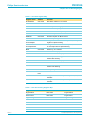
Revision History:
Version
Date
Document Status
Author(s)
01
8 October 2003
First release
Stephen Hibberd
PNX8526
Philips Semiconductors
Programmable Source Decoder with Integrated Peripherals
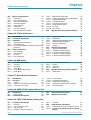
Contents
Chapter 1: Functional Specification
1.1
1.2
1.3
1.4
1.5
1.6
Introduction . . . . . . . . . . . . . . . . . . . . . . . . . . . . . . . 1
PNX8526 Feature Summary . . . . . . . . . . . . . . . 2
PNX8526 Functional Overview . . . . . . . . . . . . 2
Display Modes . . . . . . . . . . . . . . . . . . . . . . . . . . . . . 4
System Functional Overview . . . . . . . . . . . . . . 6
PNX8526 Detailed Functional Description . 9
1.6.1
1.6.2
1.6.3
1.6.4
1.6.5
1.6.6
1.6.7
1.6.8
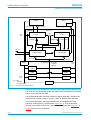
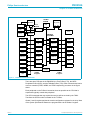
Functional Block Diagram . . . . . . . . . . . . . . . . . . . . 9
System Boot . . . . . . . . . . . . . . . . . . . . . . . . . . . . . . 10
TM32 CPU Core Processor . . . . . . . . . . . . . . . . . 11
PR3940 MIPS RISC Core . . . . . . . . . . . . . . . . . . . 11
OS Security . . . . . . . . . . . . . . . . . . . . . . . . . . . . . . . 12
2D Drawing and DMA Engine . . . . . . . . . . . . . . . 12
HL MPEG2 Decoder (VMPG). . . . . . . . . . . . . . . . 13
Video Processing and Display (MBS and AICP)
1.6.8.1
1.6.8.2
Memory Based Scaler (MBS) . . . . . . . . . . . . . . . . 14
Advanced Image Composition Processors (AICP)
1.6.8.3
1.6.8.4
1.6.9
1.6.10
. . . . . . . . . . . . . . . . . . . . . . . . . . . . . . . . . . . . . . . . . . 15
AICP Layer Structure . . . . . . . . . . . . . . . . . . . . . . . 17
AICP Mixer Structure . . . . . . . . . . . . . . . . . . . . . . . 19
PNX8510 Analog Companion Chip . . . . . . . . . . . 20
Video Input Processor (VIP) . . . . . . . . . . . . . . . . . 20
. . . . . . . . . . . . . . . . . . . . . . . . . . . . . . . . . . . . . . . . . . 13
1.6.11
1.6.12
1.6.13
1.6.14
1.6.15
1.6.16
1.6.17
1.6.17.1
1.6.17.2
1.6.18
1.6.19
1.6.20
1.6.21
1.6.22
1.6.23
1.6.24
1.7
Transport Stream Routing and MSP . . . . . . . . .
Main Memory Interface (MMI) . . . . . . . . . . . . . . .
Conditional Access Interfaces . . . . . . . . . . . . . .
Audio Interfaces (AI, AO, SPDI and SPDO) . . .
1394 Interfaces . . . . . . . . . . . . . . . . . . . . . . . . . . .
Utility DMA Controller and CRC Checker . . . . .
PCI Bus Interface Unit . . . . . . . . . . . . . . . . . . . . .
PCI Capabilities . . . . . . . . . . . . . . . . . . . . . . . . . . .
Simple Peripheral Capabilities (XIO8) . . . . . . . .
Peripherals . . . . . . . . . . . . . . . . . . . . . . . . . . . . . . .
GPIO Pins. . . . . . . . . . . . . . . . . . . . . . . . . . . . . . . .
Remote Control . . . . . . . . . . . . . . . . . . . . . . . . . . .
IR Blaster . . . . . . . . . . . . . . . . . . . . . . . . . . . . . . . .
Endianness. . . . . . . . . . . . . . . . . . . . . . . . . . . . . . .
Interrupts. . . . . . . . . . . . . . . . . . . . . . . . . . . . . . . . .
Special Display Scenarios . . . . . . . . . . . . . . . . . .
21
23
23
24
24
25
25
25
26
27
28
28
29
29
29
30
PNX8526 Internal Architecture . . . . . . . . . . . 31
1.7.1
Miscellaneous Modules . . . . . . . . . . . . . . . . . . . . 32
1.8
1.9
1.10
Power Requirements . . . . . . . . . . . . . . . . . . . . . 32
Package . . . . . . . . . . . . . . . . . . . . . . . . . . . . . . . . . . 33
Delta between PNX8525 and PNX8526 . . . 33
2.6
Alternate System Memory Map with
External Host CPU . . . . . . . . . . . . . . . . . . . . . . . 46
Chapter 2: System Memory Map and Protection
2.1
2.2
2.2.1
2.2.2
2.2.3
2.3
2.4
2.4.1
2.4.2
2.4.3
2.5
2.5.1
2.5.2
Introduction . . . . . . . . . . . . . . . . . . . . . . . . . . . . . . 34
Standard System Memory Map . . . . . . . . . . . 34
Apertures in the Standard System Memory Map
2.6.1
PCI Standard Boot and Memory Map Assembly
. . . . . . . . . . . . . . . . . . . . . . . . . . . . . . . . . . . . . . . . . . 35
Building the Standard System Memory Map . . . 36
2.6.2
Internal MIPS and External Host CPU . . . . . . . 47
Rationale for the Standard System Memory Map
2.7
. . . . . . . . . . . . . . . . . . . . . . . . . . . . . . . . . . . . . . . . . . 36
2.7.1
2.7.1.1
2.7.2
2.7.3
2.7.3.1
2.7.3.2
Hardware Limitations to Object Visibility . 37
Protection Mechanisms . . . . . . . . . . . . . . . . . . 38
Introduction . . . . . . . . . . . . . . . . . . . . . . . . . . . . . . . 38
MIPS with TLB Disabled . . . . . . . . . . . . . . . . . . . . 38
TM32 Protection Mechanisms . . . . . . . . . . . . . . . 39
Registers Descriptions . . . . . . . . . . . . . . . . . . . 40
Global 2 Registers . . . . . . . . . . . . . . . . . . . . . . . . . 41
PCI, TM32, and MIPS Aperture Control Registers
. . . . . . . . . . . . . . . . . . . . . . . . . . . . . . . . . . . . . . . . . 46
Memory Map Perspectives . . . . . . . . . . . . . . . 47
47
48
49
50
51
2.7.4
2.7.5
View from MIPS . . . . . . . . . . . . . . . . . . . . . . . . . . .
MIPS Exception Vector Logic . . . . . . . . . . . . . . .
View from the TM32 CPU Core . . . . . . . . . . . . .
View from PCI Bus . . . . . . . . . . . . . . . . . . . . . . . .
PNX8526 as PCI Configuration Manager . . . . .
An External Host CPU as PCI Configuration
Manager . . . . . . . . . . . . . . . . . . . . . . . . . . . . . . . . .
View from Fast PI-Bus . . . . . . . . . . . . . . . . . . . . .
View from M-PI and T-PI Buses . . . . . . . . . . . . .
3.5.1
3.5.2
3.5.2.1
3.5.3
3.5.4
3.5.5
3.5.5.1
External I2C Boot EEPROM Types . . . . . . . . . .
External EEPROM Boot Script Binary Format .
Binary Boot Script Endian Mode Issues . . . . . .
Details on I2C Operation . . . . . . . . . . . . . . . . . . .
Internal Host Booting Using an External Script
External Host Boot . . . . . . . . . . . . . . . . . . . . . . . .
Example of External Host Boot Script . . . . . . . .
64
65
66
66
67
67
68
51
52
54
. . . . . . . . . . . . . . . . . . . . . . . . . . . . . . . . . . . . . . . . . . 45
Chapter 3: Boot
3.1
3.2
3.3
3.4
3.4.1
3.4.2
3.4.3
3.4.4
3.5
Functional Specification . . . . . . . . . . . . . . . . . . 55
Symbolic Boot Language . . . . . . . . . . . . . . . . . 56
Internal vs. External Host Boot . . . . . . . . . . . 57
Built-In Boot Scripts . . . . . . . . . . . . . . . . . . . . . . 58
MIPS Reset Vector Re-Direction . . . . . . . . . . . . . 58
Built-In Boot Script #1 (Boot Mode 001 . . . . . . . 58
Built-In Boot Script #2 (Boot Mode 010) . . . . . . . 60
Built-In Boot Script #3, for Boot Mode 100 . . . . 62
External Boot Scripts . . . . . . . . . . . . . . . . . . . . . 64
3.6
Boot Stages and Responsibilities . . . . . . . 69
3.6.1
UM10104_1
After Stage 0 . . . . . . . . . . . . . . . . . . . . . . . . . . . . . 69
© Koninklijke Philips Electronics N.V. 2003. All rights reserved.
Rev. 01 — 8 October 2003
i
PNX8526
Philips Semiconductors
Programmable Source Decoder with Integrated Peripherals
3.6.2
Checklist . . . . . . . . . . . . . . . . . . . . . . . . . . . . . . . . . . 70
3.7
Register Descriptions . . . . . . . . . . . . . . . . . . . . 71
Chapter 4: Endian Mode
4.1
4.2
4.3
4.3.1
4.3.2
Introduction . . . . . . . . . . . . . . . . . . . . . . . . . . . . . . 72
Feature Summary . . . . . . . . . . . . . . . . . . . . . . . . . 72
Endian Mode Theory . . . . . . . . . . . . . . . . . . . . . 72
4.4.5
Law 1: The “CPU Rule” . . . . . . . . . . . . . . . . . . . . . 73
Law 2: The “DMA Convention Rule” . . . . . . . . . . 75
4.6.1
4.6.2
4.6.3
4.6.4
4.6.5
4.6.6
4.6.7
4.4
PNX8526 Endian Mode Architecture Details
4.4.1
4.4.2
4.4.3
4.4.4
. . . . . . . . . . . . . . . . . . . . . . . . . . . . . . . . . . . . . . . . . . . . 75
Global Endian Mode . . . . . . . . . . . . . . . . . . . . . . . 76
Peripheral Control. . . . . . . . . . . . . . . . . . . . . . . . . . 76
Peripheral DMA. . . . . . . . . . . . . . . . . . . . . . . . . . . . 77
SIMD Programming Issues . . . . . . . . . . . . . . . . . . 77
4.5
4.6
4.7
Optional Endian Mode Override . . . . . . . . . . . . . 78
Example: Audio In—Programmer’s View 78
Implementation Details . . . . . . . . . . . . . . . . . . 79
Endian System Block Diagram . . . . . . . . . . . . . .
DMA Across 32-Bit L2 Interface . . . . . . . . . . . . .
DMA Across PI-Bus . . . . . . . . . . . . . . . . . . . . . . .
DMA Across DVP Memory Bus . . . . . . . . . . . . .
PIO-Only Devices . . . . . . . . . . . . . . . . . . . . . . . . .
PIMI Bridge. . . . . . . . . . . . . . . . . . . . . . . . . . . . . . .
PCI Interface . . . . . . . . . . . . . . . . . . . . . . . . . . . . .
79
82
82
84
85
85
87
Detailed Example . . . . . . . . . . . . . . . . . . . . . . . . 87
Chapter 5: Clock Reset and Power Management
5.1
5.2
5.2.1
5.2.1.1
5.2.2
5.2.3
5.2.3.1
5.2.3.2
5.2.3.3
5.2.3.4
5.2.3.5
5.2.3.6
5.2.3.7
5.2.4
5.2.4.1
5.3
Introduction . . . . . . . . . . . . . . . . . . . . . . . . . . . . . . 89
Clock Module Functional Description . . . . 89
Overview . . . . . . . . . . . . . . . . . . . . . . . . . . . . . . . . . 89
Custom Analog Block (CAB) . . . . . . . . . . . . . . . . 90
Chip I/O . . . . . . . . . . . . . . . . . . . . . . . . . . . . . . . . . . 92
Operation . . . . . . . . . . . . . . . . . . . . . . . . . . . . . . . . . 94
System Level Clocks . . . . . . . . . . . . . . . . . . . . . . . 94
Sources of PNX8526 Clocks . . . . . . . . . . . . . . . . 97
PLL Programming. . . . . . . . . . . . . . . . . . . . . . . . . 100
Bypass Clock Sources . . . . . . . . . . . . . . . . . . . . . 102
Power Up and Reset Sequence . . . . . . . . . . . . 103
Powerdown . . . . . . . . . . . . . . . . . . . . . . . . . . . . . . 103
Clock Detection . . . . . . . . . . . . . . . . . . . . . . . . . . . 103
Register Descriptions . . . . . . . . . . . . . . . . . . . . . . 104
Register Address Map . . . . . . . . . . . . . . . . . . . . . 104
Reset Module Functional Description . . . 124
5.3.1
5.3.1.1
5.3.1.2
5.3.2
5.3.2.1
5.3.2.2
5.3.2.3
5.3.3
5.3.3.1
5.4
Overview . . . . . . . . . . . . . . . . . . . . . . . . . . . . . . . .
Chip I/O . . . . . . . . . . . . . . . . . . . . . . . . . . . . . . . .
Major Interfaces . . . . . . . . . . . . . . . . . . . . . . . . . .
Operation . . . . . . . . . . . . . . . . . . . . . . . . . . . . . . .
PERI_RST State Machine . . . . . . . . . . . . . . . . .
MIPS_RST State Machine. . . . . . . . . . . . . . . . .
SYS_RST_OUT State Machine . . . . . . . . . . .
Register Descriptions . . . . . . . . . . . . . . . . . . . . .
Register Address Map . . . . . . . . . . . . . . . . . . . .
125
127
127
127
128
129
130
130
130
Power Management . . . . . . . . . . . . . . . . . . . . . 132
5.4.1
5.4.1.1
5.4.1.2
5.4.2
5.4.3
5.4.3.1
Module Control . . . . . . . . . . . . . . . . . . . . . . . . . .
Device Powerdown . . . . . . . . . . . . . . . . . . . . . . .
Device Wakeup . . . . . . . . . . . . . . . . . . . . . . . . . .
CPU Idle Power . . . . . . . . . . . . . . . . . . . . . . . . . .
PNX8526 System Power Modes . . . . . . . . . . .
PCI Power Modes . . . . . . . . . . . . . . . . . . . . . . . .
132
132
133
133
134
135
6.2.4
6.2.4.1
6.2.5
6.2.6
6.2.6.1
6.2.7
Interrupt Source Register. . . . . . . . . . . . . . . . . .
Special Interrupt Service Cases . . . . . . . . . . . .
Interrupt Priority . . . . . . . . . . . . . . . . . . . . . . . . . .
Device Interrupt Registers . . . . . . . . . . . . . . . . .
Special Cases . . . . . . . . . . . . . . . . . . . . . . . . . . .
PCI Interrupt Enable Register . . . . . . . . . . . . . .
143
144
145
146
146
147
Chapter 6: Priority Interrupt Controller
6.1
6.1.1
6.1.2
6.2
6.2.1
6.2.2
6.2.3
6.2.3.1
Functional Description . . . . . . . . . . . . . . . . . . 136
Overview . . . . . . . . . . . . . . . . . . . . . . . . . . . . . . . . 136
PIC Interrupt Requests . . . . . . . . . . . . . . . . . . . . 139
Operation . . . . . . . . . . . . . . . . . . . . . . . . . . . . . . . . 140
PIC Interrupt Outputs . . . . . . . . . . . . . . . . . . . . . . 140
TriMedia Interrupt Requests . . . . . . . . . . . . . . . . 141
Inter-Processor Communication . . . . . . . . . . . . 141
IPC Registers . . . . . . . . . . . . . . . . . . . . . . . . . . . . 143
6.3
Register Descriptions . . . . . . . . . . . . . . . . . . . 148
6.3.1
Global 2 Registers . . . . . . . . . . . . . . . . . . . . . . . 154
Chapter 7: Pixel Formats
7.1
7.2
7.3
7.3.1
7.3.2
7.3.3
7.3.4
Introduction . . . . . . . . . . . . . . . . . . . . . . . . . . . . . 155
Summary of Native Pixel Formats . . . . . . . 156
Native Pixel Format Representation . . . . . 157
Indexed Formats . . . . . . . . . . . . . . . . . . . . . . . . . . 157
16-Bit/Pixel Packed Formats . . . . . . . . . . . . . . . 158
32-Bit/Pixel Packed Formats . . . . . . . . . . . . . . . 158
Packed YUV 4:2:2 Formats . . . . . . . . . . . . . . . . 159
7.3.5
7.4
7.5
7.6
7.7
7.8
Planar YUV 4:2:0 and YUV 4:2:2 Formats . . . 160
Universal Converter. . . . . . . . . . . . . . . . . . . . .
Alpha Value and Pixel Transparency . . .
RGB and YUV Values . . . . . . . . . . . . . . . . . . .
Image Storage Format . . . . . . . . . . . . . . . . . .
System Endian Mode . . . . . . . . . . . . . . . . . . .
UM10104_1
162
163
163
163
164
© Koninklijke Philips Electronics N.V. 2003. All rights reserved.
Rev. 01 — 8 October 2003
ii
PNX8526
Philips Semiconductors
Programmable Source Decoder with Integrated Peripherals
Chapter 8: PCI-XIO
8.1
8.1.1
8.1.1.1
8.1.1.2
8.1.1.3
8.1.1.4
8.2
8.2.1
8.2.2
Functional Description . . . . . . . . . . . . . . . . . . 166
Overview . . . . . . . . . . . . . . . . . . . . . . . . . . . . . . . . 166
PCI Interface . . . . . . . . . . . . . . . . . . . . . . . . . . . . . 166
PI Interface . . . . . . . . . . . . . . . . . . . . . . . . . . . . . . 167
DVP Memory Bus Interface . . . . . . . . . . . . . . . . 168
XIO Interface . . . . . . . . . . . . . . . . . . . . . . . . . . . . . 168
Operation . . . . . . . . . . . . . . . . . . . . . . . . . . . . . . . . 169
NAND-Flash Interface . . . . . . . . . . . . . . . . . . . . . 171
Motorola Style Interface . . . . . . . . . . . . . . . . . . . 176
8.2.3
8.2.4
8.2.4.1
8.2.4.2
8.2.5
8.3
NOR Flash Interface . . . . . . . . . . . . . . . . . . . . . .
IDE Description . . . . . . . . . . . . . . . . . . . . . . . . . .
Data Transfer Operation . . . . . . . . . . . . . . . . . .
Registers. . . . . . . . . . . . . . . . . . . . . . . . . . . . . . . .
PCI Interrupt Enable Register . . . . . . . . . . . . . .
178
180
182
183
185
Register Descriptions . . . . . . . . . . . . . . . . . . . 185
8.3.1
8.3.2
Register Address Map . . . . . . . . . . . . . . . . . . . . 186
Global 2 Registers . . . . . . . . . . . . . . . . . . . . . . . 204
9.9.1
Register Address Map . . . . . . . . . . . . . . . . . . . . 215
Chapter 9: Main Memory Interface (MMI)
9.1
9.2
9.2.1
9.2.2
9.3
9.3.1
9.4
9.5
9.6
9.7
9.7.1
9.7.2
9.8
9.8.1
9.8.2
9.8.3
9.9
Introduction . . . . . . . . . . . . . . . . . . . . . . . . . . . . . 205
SDRAM Configurations . . . . . . . . . . . . . . . . . . 206
Supported Chips and Configurations . . . . . . . . 206
Detailed SDRAM Specifications . . . . . . . . . . . . 206
SDRAM I/O Pins . . . . . . . . . . . . . . . . . . . . . . . . . 207
Pin Connections . . . . . . . . . . . . . . . . . . . . . . . . . . 208
SDRAM Initialization . . . . . . . . . . . . . . . . . . . . . 209
SDRAM Refresh . . . . . . . . . . . . . . . . . . . . . . . . . 210
Powerdown and Self-Refresh . . . . . . . . . . . 211
Defaults . . . . . . . . . . . . . . . . . . . . . . . . . . . . . . . . . . 212
Values for Address Bits . . . . . . . . . . . . . . . . . . . . 212
Tri-State Bus Driver . . . . . . . . . . . . . . . . . . . . . . . 212
Memory Protection . . . . . . . . . . . . . . . . . . . . . . 213
Architecture . . . . . . . . . . . . . . . . . . . . . . . . . . . . . . 213
Registers . . . . . . . . . . . . . . . . . . . . . . . . . . . . . . . . 214
Protection Behavior . . . . . . . . . . . . . . . . . . . . . . . 214
Register Descriptions . . . . . . . . . . . . . . . . . . . 215
9.10
9.10.1
9.10.2
9.10.3
9.10.3.1
9.10.3.2
9.10.3.3
9.10.3.4
9.10.3.5
9.10.3.6
9.10.4
9.10.5
9.10.6
Unified Memory Organization in PNX8526
..........................................
Introduction. . . . . . . . . . . . . . . . . . . . . . . . . . . . . .
Organization of Addresses . . . . . . . . . . . . . . . .
MPEG Memory Format . . . . . . . . . . . . . . . . . . .
General Description . . . . . . . . . . . . . . . . . . . . . .
Padding . . . . . . . . . . . . . . . . . . . . . . . . . . . . . . . . .
Frames, Fields and Pixels . . . . . . . . . . . . . . . . .
Alternate Address Space for 64-Byte Stride .
Y Pixels . . . . . . . . . . . . . . . . . . . . . . . . . . . . . . . . .
UV Pixels . . . . . . . . . . . . . . . . . . . . . . . . . . . . . . .
16.4 Motion Compensation . . . . . . . . . . . . . . . .
Storing MPEG Frames Using 32 by 4 Writes.
217
217
217
219
219
220
220
221
221
222
223
225
Reading Video Lines of Calculated MPEG Frames
. . . . . . . . . . . . . . . . . . . . . . . . . . . . . . . . . . . . . . . . 226
9.10.7
9.11
Storage of Other Video Frames . . . . . . . . . . . . 226
Performance Features . . . . . . . . . . . . . . . . . . 226
Chapter 10: GPIO/IR
10.1
10.2
10.2.1
10.2.2
10.2.2.1
Introduction . . . . . . . . . . . . . . . . . . . . . . . . . . . . . 227
Functional Description . . . . . . . . . . . . . . . . . . 227
GPIO Pin Assignment . . . . . . . . . . . . . . . . . . . . . 227
GPIO Mode Settings . . . . . . . . . . . . . . . . . . . . . . 229
GPIO mode select . . . . . . . . . . . . . . . . . . . . . . . . 229
10.2.2.2
10.2.2.3
10.2.2.4
10.3
GPIO Data Settings . . . . . . . . . . . . . . . . . . . . . . 229
Reading GPIO Pin Status . . . . . . . . . . . . . . . . . 230
Signal Monitoring and Pattern Generation . . . 230
Register Descriptions . . . . . . . . . . . . . . . . . . . 241
10.3.1
Register Address Map . . . . . . . . . . . . . . . . . . . . 242
Chapter 11: UART Ports
11.1
11.2
11.2.1
11.2.2
11.2.3
Introduction . . . . . . . . . . . . . . . . . . . . . . . . . . . . . 266
Functional Description . . . . . . . . . . . . . . . . . . 267
11.3
Transmitter and TXFIFO . . . . . . . . . . . . . . . . . . . 267
Receiver and RXFIFO . . . . . . . . . . . . . . . . . . . . . 267
Clock Settings and Baud Generator . . . . . . . . . 268
11.4
Operation . . . . . . . . . . . . . . . . . . . . . . . . . . . . . . . 268
11.3.1
Interrupts. . . . . . . . . . . . . . . . . . . . . . . . . . . . . . . . 268
Register Descriptions . . . . . . . . . . . . . . . . . . . 269
11.4.1
Register Address Map . . . . . . . . . . . . . . . . . . . . 269
12.2.2.1
12.2.2.2
12.2.3
12.2.4
DMA Modes . . . . . . . . . . . . . . . . . . . . . . . . . . . . .
DMA Buffers . . . . . . . . . . . . . . . . . . . . . . . . . . . . .
FIFOs . . . . . . . . . . . . . . . . . . . . . . . . . . . . . . . . . .
Codec Interface . . . . . . . . . . . . . . . . . . . . . . . . . .
Chapter 12: SSI Port
12.1
12.2
12.2.1
12.2.2
Introduction . . . . . . . . . . . . . . . . . . . . . . . . . . . . . 278
Functional Description . . . . . . . . . . . . . . . . . . 278
PI-Bus Interface . . . . . . . . . . . . . . . . . . . . . . . . . . 278
DMA Channels . . . . . . . . . . . . . . . . . . . . . . . . . . . 279
UM10104_1
279
280
280
280
© Koninklijke Philips Electronics N.V. 2003. All rights reserved.
Rev. 01 — 8 October 2003
iii
PNX8526
Philips Semiconductors
Programmable Source Decoder with Integrated Peripherals
12.3
12.3.1
12.3.1.1
12.3.1.2
12.4
Operation . . . . . . . . . . . . . . . . . . . . . . . . . . . . . . . . 280
Interrupts . . . . . . . . . . . . . . . . . . . . . . . . . . . . . . . . 281
Interrupt Sources . . . . . . . . . . . . . . . . . . . . . . . . . 281
Interrupt Usage . . . . . . . . . . . . . . . . . . . . . . . . . . . 282
12.4.1
12.4.2
12.5
Siemens ALIS_D PSB-4596 . . . . . . . . . . . . . . . 283
ST Microelectronics STLC-7550 . . . . . . . . . . . 283
Register Descriptions . . . . . . . . . . . . . . . . . . . 284
12.5.1
Register Address Map . . . . . . . . . . . . . . . . . . . . 284
13.2.2
13.2.3
Parameters . . . . . . . . . . . . . . . . . . . . . . . . . . . . . . 294
Powerdown Feature . . . . . . . . . . . . . . . . . . . . . . 295
Major Interfaces . . . . . . . . . . . . . . . . . . . . . . . . . 283
Chapter 13: USB Port
13.1
13.2
13.2.1
13.2.1.1
Introduction . . . . . . . . . . . . . . . . . . . . . . . . . . . . . 292
Functional Description . . . . . . . . . . . . . . . . . . 292
Operation . . . . . . . . . . . . . . . . . . . . . . . . . . . . . . . . 293
USB Data Transactions . . . . . . . . . . . . . . . . . . . . 294
13.3
Register Descriptions . . . . . . . . . . . . . . . . . . . 295
Chapter 14: IEEE 1394
14.1
14.1.1
14.2
14.2.1
14.2.1.1
14.2.2
14.2.3
14.2.4
14.2.5
14.2.6
14.2.6.1
14.2.6.2
14.2.6.3
14.2.6.4
14.2.6.5
14.2.6.6
Introduction . . . . . . . . . . . . . . . . . . . . . . . . . . . . . 304
Features . . . . . . . . . . . . . . . . . . . . . . . . . . . . . . . . . 305
Functional Description . . . . . . . . . . . . . . . . . . 306
PHY-LINK Interface . . . . . . . . . . . . . . . . . . . . . . . 306
PHY Interface Timing . . . . . . . . . . . . . . . . . . . . . . 307
Host Interface . . . . . . . . . . . . . . . . . . . . . . . . . . . . 308
Timer . . . . . . . . . . . . . . . . . . . . . . . . . . . . . . . . . . . . 308
Link Layer . . . . . . . . . . . . . . . . . . . . . . . . . . . . . . . 309
FIFO . . . . . . . . . . . . . . . . . . . . . . . . . . . . . . . . . . . . 309
AV Interface and AV Layer . . . . . . . . . . . . . . . . . 310
Isochronous IEC 61883 Transmitter . . . . . . . . . 312
Isochronous IEC 61883 Receiver . . . . . . . . . . . 313
Format of Stream Received from Link Layer . . 314
Synchronization Timestamps . . . . . . . . . . . . . . . 314
mLAN . . . . . . . . . . . . . . . . . . . . . . . . . . . . . . . . . . . 315
Digital Camera . . . . . . . . . . . . . . . . . . . . . . . . . . . 315
14.2.6.7
14.2.7
14.2.8
14.2.8.1
14.2.9
14.2.9.1
14.2.10
14.2.10.1
14.2.11
14.2.11.1
14.2.11.2
14.2.12
14.2.13
14.3
AV Receiver Interface . . . . . . . . . . . . . . . . . . . .
Content Protection . . . . . . . . . . . . . . . . . . . . . . .
Asynchronous Packet Transmitter . . . . . . . . . .
Asynchronous Transmit Packet Formats . . . .
Asynchronous Packet Receiver (ARX) . . . . . .
Asynchronous Receive Packet Formats . . . . .
Interrupts. . . . . . . . . . . . . . . . . . . . . . . . . . . . . . . .
Determining and Clearing Interrupts . . . . . . . .
Reset . . . . . . . . . . . . . . . . . . . . . . . . . . . . . . . . . . .
Reset from Host Bus Interface . . . . . . . . . . . . .
Software Reset . . . . . . . . . . . . . . . . . . . . . . . . . .
Power Management . . . . . . . . . . . . . . . . . . . . . .
IEEE 1394 Physical Configuration Register . .
316
316
316
317
322
322
328
329
331
331
331
332
332
Register Descriptions . . . . . . . . . . . . . . . . . . . 332
14.3.1
14.3.2
Register Address Map . . . . . . . . . . . . . . . . . . . . 332
Global 2 Registers . . . . . . . . . . . . . . . . . . . . . . . 357
15.3.1.7
15.3.1.8
15.3.1.9
15.3.2
15.3.2.1
15.3.2.2
15.3.2.3
15.3.2.4
Address Register and Comparator . . . . . . . . .
Data Shift Register . . . . . . . . . . . . . . . . . . . . . . .
Related Interrupts . . . . . . . . . . . . . . . . . . . . . . . .
Modes of Operation . . . . . . . . . . . . . . . . . . . . . .
Master Transmitter Mode. . . . . . . . . . . . . . . . . .
Master Receiver Mode . . . . . . . . . . . . . . . . . . . .
Slave Receiver Mode . . . . . . . . . . . . . . . . . . . . .
Slave Transmitter Mode . . . . . . . . . . . . . . . . . . .
Chapter 15: I2C Ports
15.1
15.2
15.3
15.3.1
15.3.1.1
15.3.1.2
15.3.1.3
15.3.1.4
15.3.1.5
15.3.1.6
Introduction . . . . . . . . . . . . . . . . . . . . . . . . . . . . . 358
Functional Description . . . . . . . . . . . . . . . . . . 358
Operation . . . . . . . . . . . . . . . . . . . . . . . . . . . . . . . . 360
General Operation . . . . . . . . . . . . . . . . . . . . . . . . 360
I2C Arbitration and Control Logic . . . . . . . . . . . . 360
Serial Clock Generator . . . . . . . . . . . . . . . . . . . . 361
Bit Counter . . . . . . . . . . . . . . . . . . . . . . . . . . . . . . . 361
Control Register . . . . . . . . . . . . . . . . . . . . . . . . . . 361
Status Decoder and Register . . . . . . . . . . . . . . . 361
Input Filter . . . . . . . . . . . . . . . . . . . . . . . . . . . . . . . 361
15.4
362
362
362
362
363
363
364
364
Register Descriptions . . . . . . . . . . . . . . . . . . . 365
15.4.0.1
Register Address Map . . . . . . . . . . . . . . . . . . . . 365
16.3.2.2
16.3.3
16.3.4
16.3.5
16.3.6
16.3.6.1
16.3.6.2
16.3.6.3
16.3.6.4
Programming Rules . . . . . . . . . . . . . . . . . . . . . .
Baud Rates. . . . . . . . . . . . . . . . . . . . . . . . . . . . . .
Transmission Mode . . . . . . . . . . . . . . . . . . . . . .
Reception Mode . . . . . . . . . . . . . . . . . . . . . . . . .
Activation and Deactivation Sequence . . . . . .
Activation Sequence . . . . . . . . . . . . . . . . . . . . . .
Warm Reset . . . . . . . . . . . . . . . . . . . . . . . . . . . . .
Emergency Sequence . . . . . . . . . . . . . . . . . . . .
Deactivation Sequence . . . . . . . . . . . . . . . . . . .
Chapter 16: Smartcard UART
16.1
16.1.1
16.2
16.3
16.3.1
16.3.1.1
16.3.2
16.3.2.1
Introduction . . . . . . . . . . . . . . . . . . . . . . . . . . . . . 382
Smartcard UART Interface . . . . . . . . . . . . . . . . . 382
Functional Description . . . . . . . . . . . . . . . . . . 384
Operation . . . . . . . . . . . . . . . . . . . . . . . . . . . . . . . . 385
Clock Circuitry . . . . . . . . . . . . . . . . . . . . . . . . . . . . 386
ISO UART . . . . . . . . . . . . . . . . . . . . . . . . . . . . . . . 387
Timeout Counters . . . . . . . . . . . . . . . . . . . . . . . . . 387
Counter Operation . . . . . . . . . . . . . . . . . . . . . . . . 388
UM10104_1
388
388
389
390
391
391
392
393
393
© Koninklijke Philips Electronics N.V. 2003. All rights reserved.
Rev. 01 — 8 October 2003
iv
PNX8526
Philips Semiconductors
Programmable Source Decoder with Integrated Peripherals
16.3.7
16.3.7.1
16.3.7.2
16.3.7.3
ISO UART Interrupts . . . . . . . . . . . . . . . . . . . . . . 393
Interrupt Mode . . . . . . . . . . . . . . . . . . . . . . . . . . . . 394
DMA Mode . . . . . . . . . . . . . . . . . . . . . . . . . . . . . . . 394
Interrupt Mechanism . . . . . . . . . . . . . . . . . . . . . . 394
16.4
Register Descriptions . . . . . . . . . . . . . . . . . . . 395
16.4.1
Register Address Map . . . . . . . . . . . . . . . . . . . . 395
17.3.1
17.3.1.1
17.3.1.2
17.3.2
Input Signal Descriptions . . . . . . . . . . . . . . . . . .
Parallel Mode . . . . . . . . . . . . . . . . . . . . . . . . . . . .
Serial Mode . . . . . . . . . . . . . . . . . . . . . . . . . . . . .
Digital Video/TS Interface Timing Diagrams .
18.1.1
18.1.2
Output Signal Descriptions . . . . . . . . . . . . . . . . 409
Transport Stream Interface Timing Diagrams 409
Chapter 17: DV Input Ports
17.1
17.2
17.3
Introduction . . . . . . . . . . . . . . . . . . . . . . . . . . . . . 407
DV Input to VIP . . . . . . . . . . . . . . . . . . . . . . . . . . 407
TS Mode of DV2 and DV3 . . . . . . . . . . . . . . . . 407
407
408
408
408
Chapter 18: Transport Stream Output Port
18.1
Introduction . . . . . . . . . . . . . . . . . . . . . . . . . . . . . 409
Chapter 19: DV Output Ports
19.1
19.2
Introduction . . . . . . . . . . . . . . . . . . . . . . . . . . . . . 410
Clocking the DV Output Stream . . . . . . . . . 410
19.2.1
19.3
PNX8526 Interface Clock Speeds . . . . . . . . . . 414
DV Out Pin Descriptions . . . . . . . . . . . . . . . . 414
Chapter 20: Audio Input Ports
20.1
20.1.1
20.2
20.2.1
20.2.2
20.2.3
20.2.3.1
20.3
20.3.1
20.3.2
Introduction . . . . . . . . . . . . . . . . . . . . . . . . . . . . . 416
Audio In Overview . . . . . . . . . . . . . . . . . . . . . . . . 416
Functional Description . . . . . . . . . . . . . . . . . . 416
Overview . . . . . . . . . . . . . . . . . . . . . . . . . . . . . . . . 416
External Interface . . . . . . . . . . . . . . . . . . . . . . . . . 417
Clock System . . . . . . . . . . . . . . . . . . . . . . . . . . . . 417
Clock System Operation . . . . . . . . . . . . . . . . . . . 418
Operation . . . . . . . . . . . . . . . . . . . . . . . . . . . . . . . . 419
Overview . . . . . . . . . . . . . . . . . . . . . . . . . . . . . . . . 419
Serial Data Framing . . . . . . . . . . . . . . . . . . . . . . . 420
20.3.3
20.3.3.1
20.3.4
20.3.5
20.3.6
20.3.7
20.3.8
20.3.9
20.4
Memory Data Formats . . . . . . . . . . . . . . . . . . . .
Endian Control . . . . . . . . . . . . . . . . . . . . . . . . . . .
Memory Buffers and Capture . . . . . . . . . . . . . .
Data Bus Latency and HBE . . . . . . . . . . . . . . .
Error Behavior . . . . . . . . . . . . . . . . . . . . . . . . . . .
Interrupts. . . . . . . . . . . . . . . . . . . . . . . . . . . . . . . .
Timestamp Events . . . . . . . . . . . . . . . . . . . . . . .
Diagnostic Mode . . . . . . . . . . . . . . . . . . . . . . . . .
422
422
422
422
423
423
424
424
Register Descriptions . . . . . . . . . . . . . . . . . . . 425
20.4.1
Register Address Map . . . . . . . . . . . . . . . . . . . . 426
21.3.3.1
21.3.4
21.3.4.1
21.3.4.2
21.3.5
21.3.6
21.3.7
21.3.8
21.3.9
21.3.10
Interrupt Latency . . . . . . . . . . . . . . . . . . . . . . . . .
Serial Data Framing . . . . . . . . . . . . . . . . . . . . . .
Serial Frame Limitations . . . . . . . . . . . . . . . . . .
I2S Serial Framing Example . . . . . . . . . . . . . . .
Codec Control . . . . . . . . . . . . . . . . . . . . . . . . . . .
Timestamp Events . . . . . . . . . . . . . . . . . . . . . . .
Reset . . . . . . . . . . . . . . . . . . . . . . . . . . . . . . . . . . .
Powerdown Behavior . . . . . . . . . . . . . . . . . . . . .
Data Bus Latency and HBE . . . . . . . . . . . . . . .
Error Behavior . . . . . . . . . . . . . . . . . . . . . . . . . . .
Chapter 21: Audio Output Ports
21.1
21.1.1
21.2
21.2.1
21.2.2
21.2.3
21.2.3.1
21.3
21.3.1
21.3.1.1
21.3.2
21.3.3
Introduction . . . . . . . . . . . . . . . . . . . . . . . . . . . . . 431
Audio Out Module . . . . . . . . . . . . . . . . . . . . . . . . . 431
Functional Description . . . . . . . . . . . . . . . . . . 432
Overview . . . . . . . . . . . . . . . . . . . . . . . . . . . . . . . . 432
External Interface . . . . . . . . . . . . . . . . . . . . . . . . . 432
Sample Clock Generator . . . . . . . . . . . . . . . . . . . 434
Clock System Operation . . . . . . . . . . . . . . . . . . . 435
Operation . . . . . . . . . . . . . . . . . . . . . . . . . . . . . . . . 435
Memory Data Formats . . . . . . . . . . . . . . . . . . . . . 435
Endian Control . . . . . . . . . . . . . . . . . . . . . . . . . . . 436
Audio Out MMIO Description . . . . . . . . . . . . . . . 437
Interrupts . . . . . . . . . . . . . . . . . . . . . . . . . . . . . . . . 437
21.4
437
438
439
439
440
441
441
441
442
443
Register Descriptions . . . . . . . . . . . . . . . . . . . 443
21.4.1
Register Address Map . . . . . . . . . . . . . . . . . . . . 444
Chapter 22: SPDIF Input Ports
22.1
22.2
22.2.1
Introduction . . . . . . . . . . . . . . . . . . . . . . . . . . . . . 450
Functional Description . . . . . . . . . . . . . . . . . . 450
External Interface . . . . . . . . . . . . . . . . . . . . . . . . . 451
22.3
Operation . . . . . . . . . . . . . . . . . . . . . . . . . . . . . . . 452
22.3.1
22.3.2
UM10104_1
The SPDIF Bitstream . . . . . . . . . . . . . . . . . . . . . 452
SPDIF Receiver Oversampling Clock . . . . . . . 453
© Koninklijke Philips Electronics N.V. 2003. All rights reserved.
Rev. 01 — 8 October 2003
v
PNX8526
Philips Semiconductors
Programmable Source Decoder with Integrated Peripherals
22.3.2.1
22.3.2.2
22.3.3
22.3.3.1
22.3.4
22.3.5
22.3.6
22.3.7
SPDIF Receiver Sample Rate Tolerance and
IEC60958 . . . . . . . . . . . . . . . . . . . . . . . . . . . . . . . . 453
SPDIF Receiver Jitter Tolerance . . . . . . . . . . . . 453
Memory Formats. . . . . . . . . . . . . . . . . . . . . . . . . . 454
SPDIF In Endianness . . . . . . . . . . . . . . . . . . . . . 455
SPDI_CBITSx and Channel Status Bits . . . . . . 456
SPDI_UBITSx and User Bits . . . . . . . . . . . . . . . 458
SPDI_SMPMASK and Sample Size Masking . 458
SPDI_BPTR and the Start of an IEC60958 Block
22.3.8
Signal Lock and Errors . . . . . . . . . . . . . . . . . . . . 459
. . . . . . . . . . . . . . . . . . . . . . . . . . . . . . . . . . . . . . . . . 458
22.3.8.1
22.3.8.2
22.3.9
22.3.10
22.3.11
22.3.12
22.4
LOCK and UNLOCK State Behavior . . . . . . . .
UNLOCK Error Behavior and DMA . . . . . . . . .
Interrupts. . . . . . . . . . . . . . . . . . . . . . . . . . . . . . . .
Event Timestamping . . . . . . . . . . . . . . . . . . . . . .
Bandwidth and Latency Requirements . . . . . .
Timestamping Control Register . . . . . . . . . . . .
459
460
460
461
461
462
Register Descriptions . . . . . . . . . . . . . . . . . . . 462
22.4.1
22.4.2
Register Address Map . . . . . . . . . . . . . . . . . . . . 462
Global 1 Registers . . . . . . . . . . . . . . . . . . . . . . . 471
23.4.1.2
23.4.2
23.4.2.1
IEC-60958 Parity . . . . . . . . . . . . . . . . . . . . . . . . . 477
IEC-60958 Memory Data Format . . . . . . . . . . . 477
Endianness. . . . . . . . . . . . . . . . . . . . . . . . . . . . . . 477
Chapter 23: SPDIF Output Port
23.1
23.2
23.2.1
23.3
23.3.1
23.3.1.1
23.3.2
23.4
23.4.1
23.4.1.1
Introduction . . . . . . . . . . . . . . . . . . . . . . . . . . . . . 472
Functional Description . . . . . . . . . . . . . . . . . . 473
External Interface . . . . . . . . . . . . . . . . . . . . . . . . . 473
Operation . . . . . . . . . . . . . . . . . . . . . . . . . . . . . . . . 473
SPDIF Mode . . . . . . . . . . . . . . . . . . . . . . . . . . . . . 474
Sample Rate Programming . . . . . . . . . . . . . . . . 474
Transparent Mode . . . . . . . . . . . . . . . . . . . . . . . . 474
Data Formatting . . . . . . . . . . . . . . . . . . . . . . . . . 475
IEC-60958 Serial Format . . . . . . . . . . . . . . . . . . 475
IEC-60958 Bit Cell and Preamble . . . . . . . . . . . 476
23.5
Errors and Interrupts . . . . . . . . . . . . . . . . . . . 477
23.5.1
23.5.2
23.5.3
23.5.4
23.6
DMA Error Conditions . . . . . . . . . . . . . . . . . . . .
HBE and Data Bus Latency . . . . . . . . . . . . . . .
Interrupts. . . . . . . . . . . . . . . . . . . . . . . . . . . . . . . .
Timestamp Events . . . . . . . . . . . . . . . . . . . . . . .
477
478
478
479
Register Summary and Descriptions . . . 479
23.6.1
Register Address Map . . . . . . . . . . . . . . . . . . . . 479
24.2.4.1
24.2.4.2
24.2.5
24.2.5.1
24.2.6
24.2.7
Memory Protection . . . . . . . . . . . . . . . . . . . . . . .
Endianness. . . . . . . . . . . . . . . . . . . . . . . . . . . . . .
Instruction and Data Caches . . . . . . . . . . . . . . .
Snooping. . . . . . . . . . . . . . . . . . . . . . . . . . . . . . . .
Debug Support. . . . . . . . . . . . . . . . . . . . . . . . . . .
Instruction Set Overview . . . . . . . . . . . . . . . . . .
25.7.2
25.7.3
TM32_MODID . . . . . . . . . . . . . . . . . . . . . . . . . . . 495
Endian Mode . . . . . . . . . . . . . . . . . . . . . . . . . . . . 495
Chapter 24: MIPS RISC Processor Core
24.1
24.2
24.2.1
24.2.2
24.2.3
24.2.4
Introduction . . . . . . . . . . . . . . . . . . . . . . . . . . . . . 482
Functional Description . . . . . . . . . . . . . . . . . . 482
Instruction Execution Unit . . . . . . . . . . . . . . . . . . 483
System Control Coprocessor (CP0) . . . . . . . . . 484
MAD Unit . . . . . . . . . . . . . . . . . . . . . . . . . . . . . . . . 484
Memory Architecture . . . . . . . . . . . . . . . . . . . . . . 484
485
485
485
486
486
486
Chapter 25: Internal TM32 CPU Core Processor
25.1
25.2
25.3
25.3.1
25.3.2
25.3.3
25.4
25.4.1
25.4.2
25.4.3
25.5
25.6
25.7
25.7.1
Introduction . . . . . . . . . . . . . . . . . . . . . . . . . . . . . 487
Functional Description . . . . . . . . . . . . . . . . . . 487
Memory Map . . . . . . . . . . . . . . . . . . . . . . . . . . . . . 488
25.8
DRAM Aperture. . . . . . . . . . . . . . . . . . . . . . . . . . . 488
MMIO Aperture . . . . . . . . . . . . . . . . . . . . . . . . . . . 489
Aperture1 (PI-Bus Aperture) . . . . . . . . . . . . . . . . 490
25.8.1
25.8.2
Special Event Handling . . . . . . . . . . . . . . . . . . 490
25.9.1
25.9.2
25.9.3
25.9.4
Reset and Start . . . . . . . . . . . . . . . . . . . . . . . . . . . 491
EXC (Exceptions) . . . . . . . . . . . . . . . . . . . . . . . . . 491
INT and NMI (Maskable and Non-Maskable
Interrupts) . . . . . . . . . . . . . . . . . . . . . . . . . . . . . . . . 492
Timers . . . . . . . . . . . . . . . . . . . . . . . . . . . . . . . . . . . 492
Debug Support . . . . . . . . . . . . . . . . . . . . . . . . . . 494
System Provisions . . . . . . . . . . . . . . . . . . . . . . 494
TM32_CTL . . . . . . . . . . . . . . . . . . . . . . . . . . . . . . . 494
25.9
Powerdown . . . . . . . . . . . . . . . . . . . . . . . . . . . . . 495
Partial Powerdown . . . . . . . . . . . . . . . . . . . . . . . 495
Full Powerdown . . . . . . . . . . . . . . . . . . . . . . . . . . 496
Interface Descriptions . . . . . . . . . . . . . . . . . . 496
PI-Bus Master . . . . . . . . . . . . . . . . . . . . . . . . . . .
PI-Bus Slave . . . . . . . . . . . . . . . . . . . . . . . . . . . .
PI-Bus Deadlock Issues . . . . . . . . . . . . . . . . . . .
DVP Memory Bus . . . . . . . . . . . . . . . . . . . . . . . .
496
498
498
498
25.10 Global 1 and 2 Registers . . . . . . . . . . . . . . . . 498
25.11 Register Descriptions . . . . . . . . . . . . . . . . . . . 499
25.11.1
25.11.2
25.11.3
UM10104_1
TM32 CPU Core Address Map . . . . . . . . . . . . . 499
Global 1 Registers . . . . . . . . . . . . . . . . . . . . . . . 513
Global 2 Registers . . . . . . . . . . . . . . . . . . . . . . . 514
© Koninklijke Philips Electronics N.V. 2003. All rights reserved.
Rev. 01 — 8 October 2003
vi
PNX8526
Philips Semiconductors
Programmable Source Decoder with Integrated Peripherals
Chapter 26: Video Input Processor (VIP)
26.1
26.1.1
26.1.1.1
26.1.1.2
26.1.1.3
26.1.1.4
Functional Description . . . . . . . . . . . . . . . . . . 515
Operation . . . . . . . . . . . . . . . . . . . . . . . . . . . . . . . . 516
Video Input Source . . . . . . . . . . . . . . . . . . . . . . . . 516
Video Input Formats . . . . . . . . . . . . . . . . . . . . . . . 518
Video Data Acquisition . . . . . . . . . . . . . . . . . . . . 518
Auxiliary Data Acquisition . . . . . . . . . . . . . . . . . . 521
26.1.1.5
26.1.1.6
26.1.1.7
26.1.1.8
26.2
Horizontal Video Filters . . . . . . . . . . . . . . . . . . .
Video Data Capture . . . . . . . . . . . . . . . . . . . . . .
AUX Data Capture . . . . . . . . . . . . . . . . . . . . . . .
Interrupt Generation . . . . . . . . . . . . . . . . . . . . . .
522
522
524
525
Register Descriptions . . . . . . . . . . . . . . . . . . . 525
26.2.1
Register Address Map . . . . . . . . . . . . . . . . . . . . 525
27.1.2.5
27.1.2.6
27.1.2.7
27.1.2.8
Color Key Processing . . . . . . . . . . . . . . . . . . . . .
Alpha Processing . . . . . . . . . . . . . . . . . . . . . . . .
Video Data Output . . . . . . . . . . . . . . . . . . . . . . .
Interrupt Generation . . . . . . . . . . . . . . . . . . . . . .
Chapter 27: Memory Based Scaler (MBS)
27.1
27.1.1
27.1.2
27.1.2.1
27.1.2.2
27.1.2.3
27.1.2.4
Functional Description . . . . . . . . . . . . . . . . . . 541
Overview . . . . . . . . . . . . . . . . . . . . . . . . . . . . . . . . 541
Operation . . . . . . . . . . . . . . . . . . . . . . . . . . . . . . . . 543
Task Control . . . . . . . . . . . . . . . . . . . . . . . . . . . . . 543
Video Source Controls . . . . . . . . . . . . . . . . . . . . . 545
Horizontal Video Filters . . . . . . . . . . . . . . . . . . . . 548
Vertical Video Filters . . . . . . . . . . . . . . . . . . . . . . 557
27.2
559
560
560
561
Register Descriptions . . . . . . . . . . . . . . . . . . . 562
27.2.1
Register Map Address . . . . . . . . . . . . . . . . . . . . 562
Chapter 28: Advanced Image Composition Processor (AICP)
28.1
28.2
28.3
28.4
28.5
28.6
28.6.1
28.6.2
28.6.3
28.6.4
28.6.5
28.6.6
28.6.7
28.6.8
28.6.9
Overview . . . . . . . . . . . . . . . . . . . . . . . . . . . . . . . . . 580
About Layers . . . . . . . . . . . . . . . . . . . . . . . . . . . . 580
About Mixers . . . . . . . . . . . . . . . . . . . . . . . . . . . . 581
Video Overlay . . . . . . . . . . . . . . . . . . . . . . . . . . . . 581
Supported Data Types . . . . . . . . . . . . . . . . . . . 581
Operation . . . . . . . . . . . . . . . . . . . . . . . . . . . . . . . . 584
Layer Structure . . . . . . . . . . . . . . . . . . . . . . . . . . . 584
Pixel Formatter . . . . . . . . . . . . . . . . . . . . . . . . . . . 586
Color Look-Up Table . . . . . . . . . . . . . . . . . . . . . . 586
Chroma/Color Keying . . . . . . . . . . . . . . . . . . . . . 587
Up Sampling Filter/Shift Filter. . . . . . . . . . . . . . . 588
Color Space Matrix . . . . . . . . . . . . . . . . . . . . . . . . 589
Down Filter . . . . . . . . . . . . . . . . . . . . . . . . . . . . . . . 590
Screen Timing Generator . . . . . . . . . . . . . . . . . . 590
Programming the STG . . . . . . . . . . . . . . . . . . . . . 592
28.6.10
28.6.11
28.6.12
28.6.13
28.6.13.1
28.6.13.2
28.6.13.3
28.6.14
28.6.15
28.6.15.1
28.6.15.2
28.7
593
593
596
597
598
598
598
599
601
601
602
Dynamic Reprogramming. . . . . . . . . . . . . . . 603
28.7.1
28.8
Changing Timing . . . . . . . . . . . . . . . . . . . . . . . . .
Mixer . . . . . . . . . . . . . . . . . . . . . . . . . . . . . . . . . . .
Alpha-Blending . . . . . . . . . . . . . . . . . . . . . . . . . .
Output Formatter . . . . . . . . . . . . . . . . . . . . . . . . .
Single Stream Mode . . . . . . . . . . . . . . . . . . . . . .
Interleaving Mode . . . . . . . . . . . . . . . . . . . . . . . .
Combined Mode . . . . . . . . . . . . . . . . . . . . . . . . .
VBI Insertion. . . . . . . . . . . . . . . . . . . . . . . . . . . . .
Hardware Software Interface . . . . . . . . . . . . . .
What the Software Needs . . . . . . . . . . . . . . . . .
Hardware Implementation . . . . . . . . . . . . . . . . .
Programming Restrictions . . . . . . . . . . . . . . . . . 603
Register Summary and Descriptions . . . 604
Chapter 29: 2D Drawing Engine
29.1
29.2
29.2.1
29.2.2
29.2.3
29.2.4
29.2.5
29.3
Overview . . . . . . . . . . . . . . . . . . . . . . . . . . . . . . . . . 627
Operation . . . . . . . . . . . . . . . . . . . . . . . . . . . . . . . . 627
Raster Operations . . . . . . . . . . . . . . . . . . . . . . . . 628
Alpha-Blending . . . . . . . . . . . . . . . . . . . . . . . . . . . 628
Source Data Location and Type . . . . . . . . . . . . 629
Patterns . . . . . . . . . . . . . . . . . . . . . . . . . . . . . . . . . 629
Transparency . . . . . . . . . . . . . . . . . . . . . . . . . . . . 630
29.3.1
29.3.2
29.3.3
29.3.4
29.3.5
29.4
Mono Expand . . . . . . . . . . . . . . . . . . . . . . . . . . . .
Mono BLT Register Setup . . . . . . . . . . . . . . . . .
Solid Fill Setup . . . . . . . . . . . . . . . . . . . . . . . . . . .
Color BLT Setup . . . . . . . . . . . . . . . . . . . . . . . . .
PatRam . . . . . . . . . . . . . . . . . . . . . . . . . . . . . . . . .
630
631
632
632
633
Register Descriptions . . . . . . . . . . . . . . . . . . . 634
29.4.1
Register Address Maps . . . . . . . . . . . . . . . . . . . 634
30.3.1
Transport Stream Interface Timing Diagrams 658
Programming Information . . . . . . . . . . . . . . . 630
Chapter 30: Transport Stream Network
30.1
30.2
30.3
Introduction . . . . . . . . . . . . . . . . . . . . . . . . . . . . . 655
TS Input Interface . . . . . . . . . . . . . . . . . . . . . . . . 656
TS Input Router . . . . . . . . . . . . . . . . . . . . . . . . . . 656
30.4
Register Descriptions . . . . . . . . . . . . . . . . . . . 660
UM10104_1
© Koninklijke Philips Electronics N.V. 2003. All rights reserved.
Rev. 01 — 8 October 2003
vii
PNX8526
Philips Semiconductors
Programmable Source Decoder with Integrated Peripherals
Chapter 31: Transport Stream Direct Memory Access
31.1
31.2
31.2.1
31.3
31.3.1
Introduction . . . . . . . . . . . . . . . . . . . . . . . . . . . . . 662
Functional Description . . . . . . . . . . . . . . . . . . 662
Output Signal Descriptions . . . . . . . . . . . . . . . . . 663
Operation . . . . . . . . . . . . . . . . . . . . . . . . . . . . . . . . 663
DMA Operation . . . . . . . . . . . . . . . . . . . . . . . . . . . 663
31.3.1.1
31.3.1.2
31.3.1.3
31.3.2
31.4
Memory Data Formats . . . . . . . . . . . . . . . . . . . .
DMA Channel Control . . . . . . . . . . . . . . . . . . . .
Packet Delivery Schedule . . . . . . . . . . . . . . . . .
Stream Control. . . . . . . . . . . . . . . . . . . . . . . . . . .
664
664
665
665
Register Summary and Descriptions . . . 666
Chapter 32: DMA Controller and CRC Checker
32.1
32.1.1
32.2
32.2.1
32.2.1.1
32.2.2
32.2.3
32.3
32.3.1
Introduction . . . . . . . . . . . . . . . . . . . . . . . . . . . . . 673
Features . . . . . . . . . . . . . . . . . . . . . . . . . . . . . . . . . 674
Functional Description . . . . . . . . . . . . . . . . . . 674
DMA Engine Core. . . . . . . . . . . . . . . . . . . . . . . . . 674
The DMA Engine Core Operation . . . . . . . . . . . 675
DMA and CRC Data Path . . . . . . . . . . . . . . . . . . 676
DMA Scatter-Gather and Control Engine . . . . . 676
DMA Transfer Operation . . . . . . . . . . . . . . . . . 676
Demand Mode DMA . . . . . . . . . . . . . . . . . . . . . . 677
32.3.2
32.3.2.1
32.3.3
32.4
Scatter-Gather DMA . . . . . . . . . . . . . . . . . . . . . . 677
Scatter-Gather Mode Retriggering . . . . . . . . . . 678
CRC Computation . . . . . . . . . . . . . . . . . . . . . . . . 679
Register Descriptions . . . . . . . . . . . . . . . . . . . 679
32.4.1
32.4.2
32.4.3
32.4.3.1
32.4.4
Configuration Registers . . . . . . . . . . . . . . . . . . .
Channel Link List Pointer Register. . . . . . . . . .
CRC Register . . . . . . . . . . . . . . . . . . . . . . . . . . . .
DMA Status Register . . . . . . . . . . . . . . . . . . . . .
Register Address Map . . . . . . . . . . . . . . . . . . . .
679
679
680
680
680
33.2.4
33.2.5
33.2.6
33.2.7
De-Scrambler Core . . . . . . . . . . . . . . . . . . . . . . .
Memory Queue Manager Controller . . . . . . . .
MPEG System Processor Interrupt Handler .
MSP Interrupt Sources and Control . . . . . . . . .
694
695
696
696
Chapter 33: MPEG System Processor (MSP)
33.1
33.1.1
33.2
33.2.1
33.2.2
33.2.2.1
33.2.2.2
33.2.2.3
33.2.2.4
33.2.2.5
33.2.2.6
33.2.3
Introduction . . . . . . . . . . . . . . . . . . . . . . . . . . . . . 687
MSP Features . . . . . . . . . . . . . . . . . . . . . . . . . . . . 688
Functional Description . . . . . . . . . . . . . . . . . . 689
GP/HS Data Interface . . . . . . . . . . . . . . . . . . . . . 689
Packet Framer . . . . . . . . . . . . . . . . . . . . . . . . . . . . 690
Framer FIFO . . . . . . . . . . . . . . . . . . . . . . . . . . . . . 691
PID Filter (TS Parsing/PS Parsing) . . . . . . . . . . 691
Local Header Unit and Timestamp Insertion
Support . . . . . . . . . . . . . . . . . . . . . . . . . . . . . . . . . . 691
Transport/De-Multiplexer RISC Engine . . . . . . 692
Transport RISC Engine Memories . . . . . . . . . . 693
Transport Parsing and De-Multiplexing . . . . . . 693
Hardware Section Filtering . . . . . . . . . . . . . . . . . 693
33.3
Register Summary and Descriptions . . . 697
33.3.1
33.3.1.1
33.3.1.2
33.3.1.3
33.3.2
33.3.3
33.3.4
33.3.5
Clarifications. . . . . . . . . . . . . . . . . . . . . . . . . . . . .
Memory Queue Manager Registers. . . . . . . . .
Data Queue Head Pointer Register . . . . . . . . .
MSP Base Address . . . . . . . . . . . . . . . . . . . . . . .
PID Filter Registers . . . . . . . . . . . . . . . . . . . . . . .
RISC Engine Registers . . . . . . . . . . . . . . . . . . .
PI-Bus Configuration Registers . . . . . . . . . . . .
MSP Interrupt Registers. . . . . . . . . . . . . . . . . . .
697
697
697
697
711
712
717
717
34.3.4
34.3.5
34.3.5.1
34.3.5.2
34.3.5.3
34.3.5.4
Interrupt. . . . . . . . . . . . . . . . . . . . . . . . . . . . . . . . .
Error Handling . . . . . . . . . . . . . . . . . . . . . . . . . . .
Unexpected Start Code . . . . . . . . . . . . . . . . . . .
MC Flush . . . . . . . . . . . . . . . . . . . . . . . . . . . . . . .
Timeout . . . . . . . . . . . . . . . . . . . . . . . . . . . . . . . . .
Reset . . . . . . . . . . . . . . . . . . . . . . . . . . . . . . . . . . .
725
725
726
727
727
728
Chapter 34: MPEG Video Decoder
34.1
34.2
34.3
34.3.1
34.3.2
34.3.3
34.3.3.1
34.3.3.2
34.3.3.3
34.3.3.4
34.3.3.5
34.3.3.6
34.3.3.7
34.3.3.8
34.3.3.9
Introduction . . . . . . . . . . . . . . . . . . . . . . . . . . . . . 720
MPEG-PIPE Overview . . . . . . . . . . . . . . . . . . . 721
VLD Operation . . . . . . . . . . . . . . . . . . . . . . . . . . . 721
VLD Input . . . . . . . . . . . . . . . . . . . . . . . . . . . . . . . . 722
VLD Output . . . . . . . . . . . . . . . . . . . . . . . . . . . . . . 722
VLD Registers . . . . . . . . . . . . . . . . . . . . . . . . . . . . 722
VLD Status (VLD_MC_STATUS) . . . . . . . . . . . 722
VLD Interrupt Enable (VLD_IE) . . . . . . . . . . . . . 723
VLD Control (VLD_CTL) . . . . . . . . . . . . . . . . . . . 723
VLD DMA Current Read Address
(VLD_INP_ADR) and VLD DMA Current Read
Count (VLD_INP_CNT) . . . . . . . . . . . . . . . . . . . . 723
VLD Command (VLD_COMMAND) . . . . . . . . . 724
VLD Shift Register (VLD_SR) . . . . . . . . . . . . . . 725
VLD Quantizer Scale (VLD_QS) . . . . . . . . . . . . 725
VLD Picture Info (VLD_PI) . . . . . . . . . . . . . . . . . 725
VLD Bit Count (VLD_BIT_CNT) . . . . . . . . . . . . . 725
34.4
Run-Length Decoder/Inverse Scan
Overview . . . . . . . . . . . . . . . . . . . . . . . . . . . . . . . . 729
34.4.1
34.4.2
34.4.3
34.4.4
34.4.5
34.4.5.1
34.4.5.2
UM10104_1
Run-Length Decoder . . . . . . . . . . . . . . . . . . . . .
Inverse Scan . . . . . . . . . . . . . . . . . . . . . . . . . . . .
Inverse Quantization. . . . . . . . . . . . . . . . . . . . . .
Quantization Coefficients for Half-Resolution
Scheme . . . . . . . . . . . . . . . . . . . . . . . . . . . . . . . . .
RL/IQ Registers . . . . . . . . . . . . . . . . . . . . . . . . . .
Run-Length Decoder Statistics Registers . . . .
Inverse Quantization Control Register
(IQ_CONTROL) . . . . . . . . . . . . . . . . . . . . . . . . . .
730
730
730
732
732
732
733
© Koninklijke Philips Electronics N.V. 2003. All rights reserved.
Rev. 01 — 8 October 2003
viii
PNX8526
Philips Semiconductors
Programmable Source Decoder with Integrated Peripherals
34.5
34.5.1
34.5.2
34.5.3
34.5.4
34.5.5
34.5.6
34.5.7
34.5.8
Motion Compensation . . . . . . . . . . . . . . . . . . . 733
Introduction . . . . . . . . . . . . . . . . . . . . . . . . . . . . . . 733
MC Control Registers . . . . . . . . . . . . . . . . . . . . . 734
MC Command Register . . . . . . . . . . . . . . . . . . . . 734
MC Status Register . . . . . . . . . . . . . . . . . . . . . . . 735
MC_PFCOUNT . . . . . . . . . . . . . . . . . . . . . . . . . . . 735
LINE_SIZE . . . . . . . . . . . . . . . . . . . . . . . . . . . . . . . 735
VLD_MC_STATUS. . . . . . . . . . . . . . . . . . . . . . . . 735
Error Concealment Operation . . . . . . . . . . . . . . 736
34.5.9
34.5.10
34.5.11
34.5.12
34.5.13
34.5.14
34.5.15
34.5.16
34.6
Bitstream Error Detection . . . . . . . . . . . . . . . . .
Options for Reducing Memory Bandwidth . . .
Fetching Macroblocks . . . . . . . . . . . . . . . . . . . .
Storing Macroblocks . . . . . . . . . . . . . . . . . . . . . .
MC/VLD Error Recovery . . . . . . . . . . . . . . . . . .
MPEG Software Reset . . . . . . . . . . . . . . . . . . . .
MC Flush . . . . . . . . . . . . . . . . . . . . . . . . . . . . . . .
MC Timeout . . . . . . . . . . . . . . . . . . . . . . . . . . . . .
737
738
738
739
740
740
740
741
Register Summary and Descriptions . . . 741
Chapter 35: PI-Bus Architecture
35.1
35.2
35.3
35.3.1
35.3.2
35.3.2.1
35.4
35.4.1
35.4.2
35.4.3
35.4.3.1
Introduction . . . . . . . . . . . . . . . . . . . . . . . . . . . . . 756
Functional Description . . . . . . . . . . . . . . . . . . 756
Operation . . . . . . . . . . . . . . . . . . . . . . . . . . . . . . . . 758
Tuning System Performance . . . . . . . . . . . . . . . 758
Bus Performance . . . . . . . . . . . . . . . . . . . . . . . . . 759
Round-Robin Arbitration Scheme (Chosen for the
PI-Buses) . . . . . . . . . . . . . . . . . . . . . . . . . . . . . . . . 759
PI-Bus Controllers . . . . . . . . . . . . . . . . . . . . . . . 760
Bus Arbitration. . . . . . . . . . . . . . . . . . . . . . . . . . . . 760
Slave Selector . . . . . . . . . . . . . . . . . . . . . . . . . . . . 761
PI Slave . . . . . . . . . . . . . . . . . . . . . . . . . . . . . . . . . 761
Error Generation . . . . . . . . . . . . . . . . . . . . . . . . . . 761
35.4.4
35.4.5
35.4.6
35.4.7
35.4.7.1
35.4.8
35.5
Interrupt Generation . . . . . . . . . . . . . . . . . . . . . .
Null Module . . . . . . . . . . . . . . . . . . . . . . . . . . . . .
MIPS External Write Buffer Empty . . . . . . . . . .
MIPS Remapping Registers . . . . . . . . . . . . . . .
Typical Programming . . . . . . . . . . . . . . . . . . . . .
Timeout . . . . . . . . . . . . . . . . . . . . . . . . . . . . . . . . .
762
762
762
762
764
764
Register Descriptions . . . . . . . . . . . . . . . . . . . 765
35.5.1
35.5.1.1
35.5.1.2
35.5.1.3
35.5.1.4
Register Address Maps . . . . . . . . . . . . . . . . . . .
PI Bridge and PIMI Registers . . . . . . . . . . . . .
F-PI Bus Controller Registers . . . . . . . . . . . . . .
M-PI Bus Controller Registers . . . . . . . . . . . . .
T-PI Bus Controller Registers . . . . . . . . . . . . . .
765
766
770
776
780
36.1.4.1
36.1.5
36.1.6
36.1.7
Buddy Mode Default Agents . . . . . . . . . . . . . . .
Hunting . . . . . . . . . . . . . . . . . . . . . . . . . . . . . . . . .
Agent IDs . . . . . . . . . . . . . . . . . . . . . . . . . . . . . . .
Dual Lists . . . . . . . . . . . . . . . . . . . . . . . . . . . . . . .
786
786
787
787
Chapter 36: MMI Arbiter
36.1
36.1.1
36.1.2
36.1.3
36.1.3.1
36.1.4
Functional Description . . . . . . . . . . . . . . . . . . 784
Overview . . . . . . . . . . . . . . . . . . . . . . . . . . . . . . . . 784
Boot Mode . . . . . . . . . . . . . . . . . . . . . . . . . . . . . . . 784
Linear Mode . . . . . . . . . . . . . . . . . . . . . . . . . . . . . . 784
Linear Mode Default Agents . . . . . . . . . . . . . . . . 785
Buddy Mode . . . . . . . . . . . . . . . . . . . . . . . . . . . . . 785
36.2
Register Summary and Descriptions . . . 787
36.2.1
Clarifications. . . . . . . . . . . . . . . . . . . . . . . . . . . . . 787
37.2.2.2
37.2.2.3
37.2.2.4
37.2.3
37.2.4
TAP Controller . . . . . . . . . . . . . . . . . . . . . . . . . . .
Boundary-Scan Register . . . . . . . . . . . . . . . . . .
JTAG Public Instruction Set . . . . . . . . . . . . . . .
Boundary-Scan Description Language . . . . . .
More Information . . . . . . . . . . . . . . . . . . . . . . . . .
Chapter 37: Boundary-Scan Hardware
37.1
37.2
37.2.1
37.2.2
37.2.2.1
Introduction . . . . . . . . . . . . . . . . . . . . . . . . . . . . . 792
Overview . . . . . . . . . . . . . . . . . . . . . . . . . . . . . . . . . 792
Testing . . . . . . . . . . . . . . . . . . . . . . . . . . . . . . . . . . 793
IEEE 1149.1 Boundary-Scan Standard . . . . . . 794
Test Access Port (TAP) . . . . . . . . . . . . . . . . . . . . 795
796
798
798
798
799
Chapter 38: MIPS EJTAG Software Debug Port
38.1
38.1.1
38.2
Introduction . . . . . . . . . . . . . . . . . . . . . . . . . . . . . 800
Using EJTAG . . . . . . . . . . . . . . . . . . . . . . . . . . . . . 800
38.3
38.4
External Pin Descriptions . . . . . . . . . . . . . . . 803
Register Descriptions . . . . . . . . . . . . . . . . . . 804
Functional Description . . . . . . . . . . . . . . . . . . 800
Chapter 39: TM32 JTAG Software Debug Port
39.1
39.1.1
39.1.1.1
39.1.1.2
39.1.1.3
Functional Description . . . . . . . . . . . . . . . . . . 807
Overview . . . . . . . . . . . . . . . . . . . . . . . . . . . . . . . . 807
Test Access Port (TAP) . . . . . . . . . . . . . . . . . . . . 807
TAP Controller . . . . . . . . . . . . . . . . . . . . . . . . . . . . 808
PNX8526 JTAG Instruction Set . . . . . . . . . . . . . 810
39.1.2
39.2
Operation . . . . . . . . . . . . . . . . . . . . . . . . . . . . . . . 810
Programming Information . . . . . . . . . . . . . . 812
39.2.1
39.2.1.1
UM10104_1
Handshaking and Communication Protocol . . 812
Transfer from Debug Front-End to Debug
Monitor . . . . . . . . . . . . . . . . . . . . . . . . . . . . . . . . . 812
© Koninklijke Philips Electronics N.V. 2003. All rights reserved.
Rev. 01 — 8 October 2003
ix
PNX8526
Philips Semiconductors
Programmable Source Decoder with Integrated Peripherals
39.2.1.2
39.2.1.3
39.2.1.4
Transfer from Monitor to Front-End . . . . . . . 812
Controller States. . . . . . . . . . . . . . . . . . . . . . . . . 812
Example Data Transfer Via JTAG . . . . . . . . . 812
39.2.1.5
39.3
Transfer of Data to TriMedia Via JTAG . . . . 813
Register Descriptions . . . . . . . . . . . . . . . . . . . 813
UM10104_1
© Koninklijke Philips Electronics N.V. 2003. All rights reserved.
Rev. 01 — 8 October 2003
x
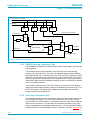
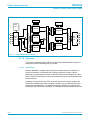
Chapter 1: Functional Specification
Programmable Source Decoder with Integrated
Peripherals
Rev. 01 — 8 October 2003
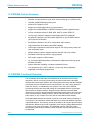
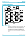
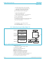
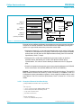
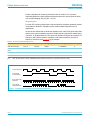
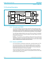
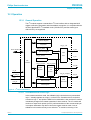
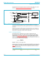
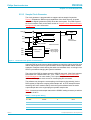
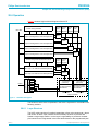
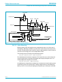
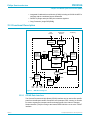
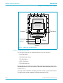
1.1 Introduction
The PNX8526 is a highly integrated media processor intended for deployment in
Advanced Set Top Box (ASTB) and Digital Television (DTV) systems. The PNX8526
is targeted at the mid to high-end ASTB/DTV systems, focusing on decoding “all
format” HD and SD MPEG2 source material with standard definition (SD), or double
line-rate SD display capabilities. This assumption implies that although the PNX8526
can process high level input formats, its display capabilities are primarily targeted at
the hundreds of millions of NTSC, PAL, and SECAM television sets in use. It is also
targeted at lower cost DTVs: those DTVs that are not considered high definition.
Progressive output is also available for double line-rate television displays or for high
resolution graphic content to be displayed on a computer monitor. The PNX8526 is
designed in a high performance 0.12 micron process.
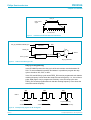
The PNX8526 is responsible for the source decode functions in ASTB/DTV systems.
These functions include conditional access, MPEG2 transport stream de-mux,
MPEG2 video decode, audio decode and processing, graphics generation, video
processing, and image composition and display. A 32-bit 200 MHz VLIW processor,
referred to as the TriMedia 3200 CPU core (TM32G CPU), carries out the majority of
media processing operations performed by the PNX8526. Fixed function hardware
will perform some operations that are not handled by the TM32 CPU. Additionally, the
PNX8526 supports a number of peripheral interfaces such as I2C, USB, IDE and
UART. Additional interfaces such as IEEE-1284 and Ethernet are supported via
Super I/O devices that reside on a PCI expansion bus. This bus also provides for
glueless interface to 8-bit wide slave devices, such as Flash/ROM, DOCSIS modem,
UARTs, etc.
An embedded MIPS processor (PR3940) running at 150 MHz is intended to run the
OS. (There is no direct support for an external processor; however, a CPU of any
type may be connected to the PNX8526 via the PCI interface.) This implies a
complete CPU subsystem consisting of the CPU itself, local memory, and an
interface to PCI. The MIPS processor is primarily responsible for control functions
and graphics-intensive operating systems, while the TM32 CPU is responsible for
running all real-time media processing functions. All resources supported within the
PNX8526 are accessible by both the MIPS processor and the TM32 CPU. The
software documentation of the PNX8526 provides more details on the interaction
between the MIPS and the TM32 CPU.
The PNX8526 is intended to be used with a small companion IC, the PNX8510. This
analog companion chip provides the majority of analog video and audio support for
the output of the PNX8526. The PNX8510 companion is capable of simultaneously
driving two video channels (6 DACs) and two stereo audio channels (4 DACs).
PNX8526
Philips Semiconductors
Chapter 1: Functional Specification
1.2 PNX8526 Feature Summary
•
200 MHz, 5 instruction/clock cycle 32-bit VLIW processing core (TM32G CPU)
•
150 MHz, MIPS PR3940 processing core
•
External CPU support via PCI
•
Support for multiple digital video (D1) input streams
•
Support for multiple MPEG2 or DIRECTV transport streams (parallel format)
•
On-chip conditional access for DVB, DES, MULTI2, ICAM, DIRECTV
•
On-chip copy protection support for OpenCable and ATSC (NRSS-B)
•
Simultaneous decode of two SD streams (MPEG2) or one HD MPEG Stream
(AFD style HD-SD decode)
•
Simultaneous decode of two AC-3 or equivalent audio streams
•
High performance 2D rendering and DMA capability
•
Dual image composition/screen refresh engines: four layer primary output, two
layer secondary output
•
Multiple channel output to support watch/record and multi-room modes
•
Embedded 1394 link layer with 5C copy protection
•
Soft modem support via SSI interface
•
16, 32, and 64 MB Unified Memory Architecture implemented with high speed
SDRAM (166 MHz)
•
System expansion capability via industry standard PCI bus
•
Core peripherals (I2C, UART, USB, etc.) on the chip, other peripherals
supported via third-party SuperIO chip
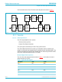
1.3 PNX8526 Functional Overview
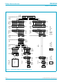
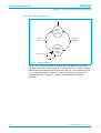
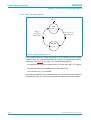
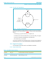
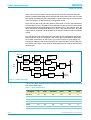
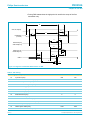
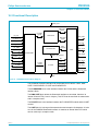
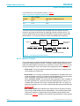
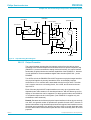
The functionality achieved within the PNX8526 can be divided into three major
categories: decode, processing, and display. Decode functions take input data
streams and convert those streams into memory based structures that the PNX8526
may further process. Decode functions may be simple, as in the case of storing D1
video into memory, or substantially more complex, as in the case of MPEG2.
Processing functions are those that modify an existing data structure and prepare
that structure for display functions. Display functions take the processed data
structures from memory and generate the appropriate output stream. As in the case
of the decode functions, display functions can be relatively simple, such as an I2S
audio output, or very complex, as in the case of multi-channel video display.
All decoded data structures are stored in memory, even when further processing is
not required. This mechanism implies that there is no direct path between input and
output data streams. The memory serves as the buffer to de-couple input and output
data streams. Based on the mode of operation, there may be multiple data structures
in memory for a given input stream. The PNX8526 uses the TM32 CPU and a
timestamping mechanism to determine when a specific memory data structure is to
be displayed.
UM10104_1
© Koninklijke Philips Electronics N.V. 2002. All rights reserved.
Rev. 01 — 8 October 2003
1-2
PNX8526
Philips Semiconductors
Chapter 1: Functional Specification
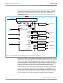
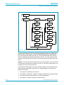
The PNX8526 implements the required decode, processing, and display functions
with a combination of fixed function hardware and TM32 CPU software modules. The
MIPS processor is not intended to be involved with the three primary function types,
other than to control them. The PNX8526 provides a good balance between those
functions that are implemented in fixed hardware and those that are programmed to
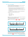
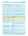
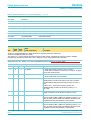
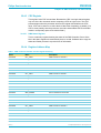
run on the TM32 CPU. The following tables illustrate how the major tasks are
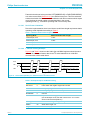
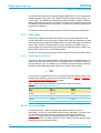
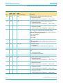
implemented under each of the three main functional areas.
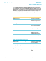
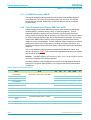
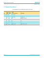
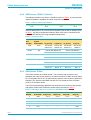
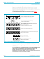
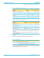
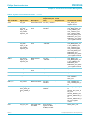
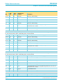
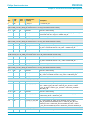
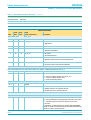
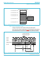
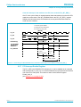
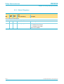
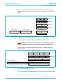
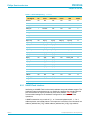
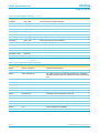
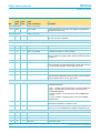
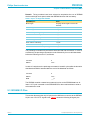
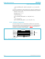
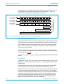
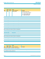
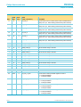
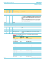
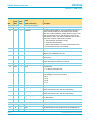
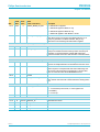
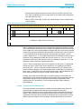
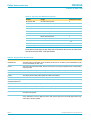
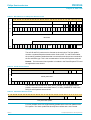
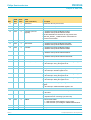
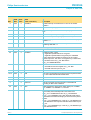
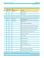
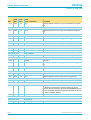
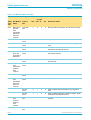
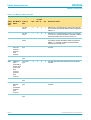
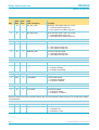
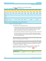
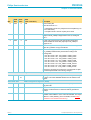
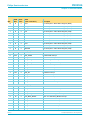
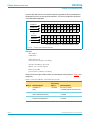
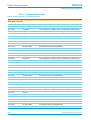
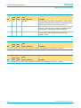
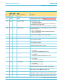
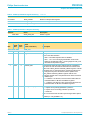
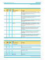
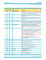
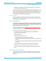
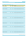
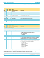
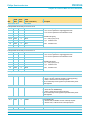
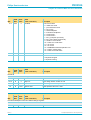
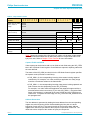
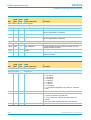
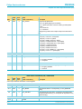
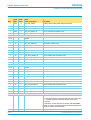
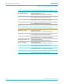
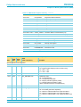
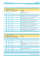
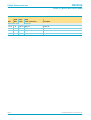
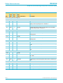
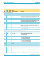
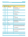
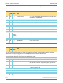
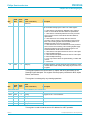
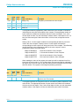
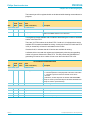
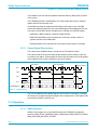
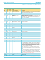
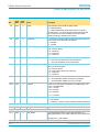
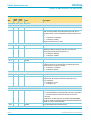
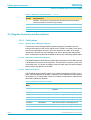
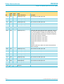
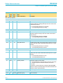
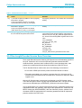
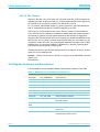
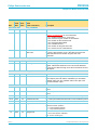
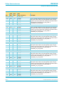
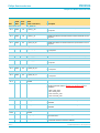
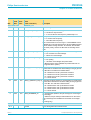
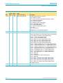
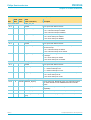
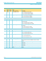
Table 1: Decode Function Responsibilities
Decode Functions
TM32 CPU Hardware Comments
D1 digital video input
X
Video Input Processor (VIP)
Section filtering
X
Programmable hardware, with
transparent mode to escape to
software if a new provider uses
an unforeseen method
PID filtering
X
Transport de-mux
X
Flexible hardware, with option to
perform transparent mode and
do de-mux in software for ATSC/
other
MPEG2 decode
X
Complete MPEG2 algorithm
below slice level
MPEG2 decode
X
Conditional access
Above slice level
X
Audio decode
X
DVB, MULTI2, ICAM, DES,
DIRECTV internal to the
PNX8526, POD, CI external
Two AC-3 streams or equivalent
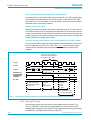
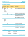
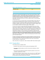
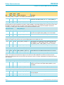
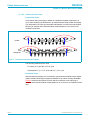
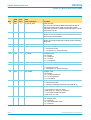
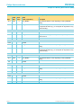
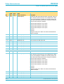
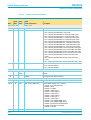
Table 2: Processing Function Responsibilities
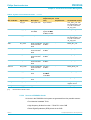
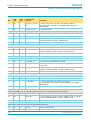
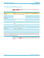
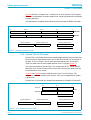
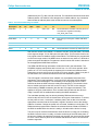
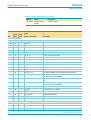
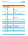
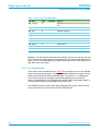
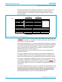
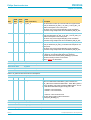
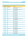
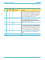
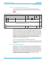
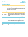
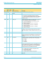
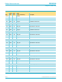
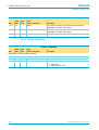
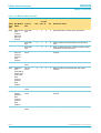
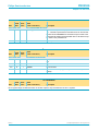
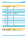
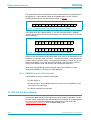
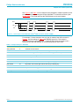
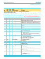
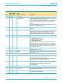
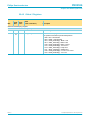
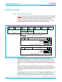
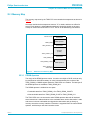
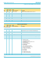
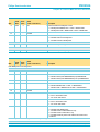
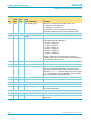
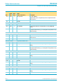
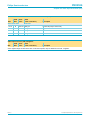
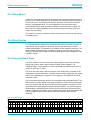
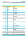
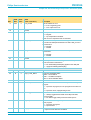
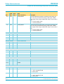
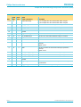
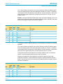
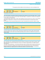
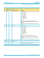
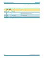
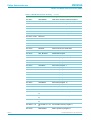
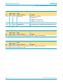
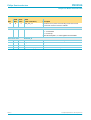
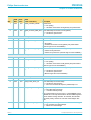
Processing Functions
Audio processing
TM32CPU Hardware Comments
X
Processing and mixing of various
PCM or AC-3 streams
2D Rendering and DMA
X
Primary video processing
X
Display CSC Matrix, CLUT, BCS,
gamma correction
X
Advanced video processing
X
UM10104_1
Scaling, anti-flicker, and deinterlacing
Algorithms not in hardware may
run on TM32 CPU (as bandwidth
allows)
© Koninklijke Philips Electronics N.V. 2002. All rights reserved.
Rev. 01 — 8 October 2003
1-3
PNX8526
Philips Semiconductors
Chapter 1: Functional Specification
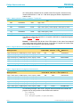
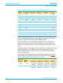
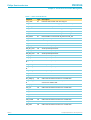
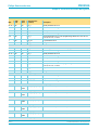
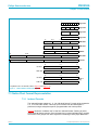
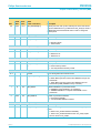
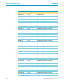
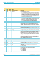
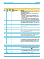
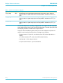
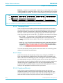
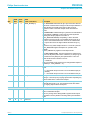
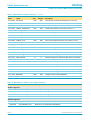
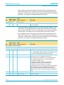
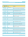
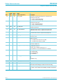
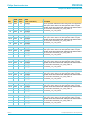
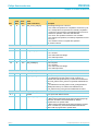
Table 2: Processing Function Responsibilities …Continued
Processing Functions
TM32CPU Hardware Comments
V.34, V.90 modem
X
Transport stream creation
X
Transport stream creation
X
Partial transport stream for
transmission across 1394 (simple
derivative of input stream)
Transport stream assembly for
transmission across 1394
(intelligently assembled stream)
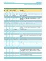
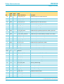
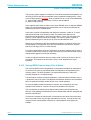
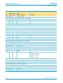
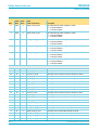
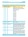
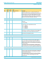
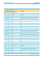
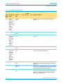
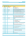
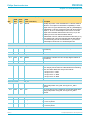
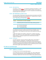
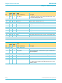
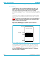
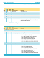
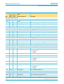
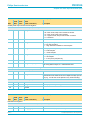
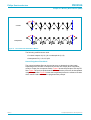
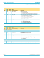
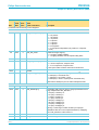
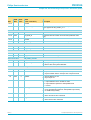
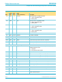
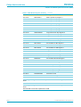
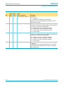
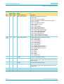
Table 3: Display Function Responsibilities
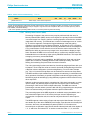
Display Features
TM32CPU Hardware Comments
Video stream
composition
Audio stream
composition
X
Advanced Image Composition Processor
(AICP)
X
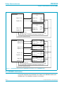
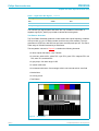
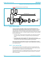
1.4 Display Modes
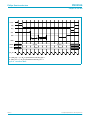
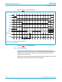
Table shows the supported display resolutions that provide acceptable performance,
features and quality. The PNX8526 is primarily intended to drive standard definition
analog television sets and low cost digital televisions. The PNX8526 is not intended
to support full high definition (HD) output nor does it support on-chip high end image
enhancement. However, the PNX8526 display capabilities are programmable, and a
wide variety of display systems can be supported.
The PNX8526 supports two simultaneous output video channels: primary and
secondary. In a watch/record scenario, the primary channel is intended to be the
viewable channel. It will display a fully composited video image consisting of PIPs,
menus, and other graphical information. The secondary channel is intended to be the
recordable channel.
Other uses are possible. For example; external high-end image enhancement can be
applied to the secondary display output channel, and brought back in to the PNX8526
through the third video input, and blended with graphics for emission through the
primary display channel.
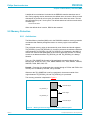
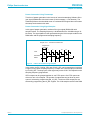
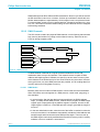
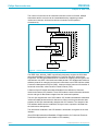
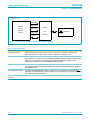
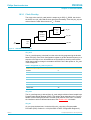
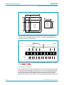
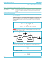
The PNX8526 hosts two independent Advanced Image Composition Processor
(AICP) modules. The primary AICP contains four image layers and is mainly intended
to be connected to a TV or monitor. The second AICP contains two layers and is
intended to connect to a VCR. The layers have their own pixel clock and frame timing
generator for fully independent display modes. Because of the independence of the
layers, a wide variety of scenarios is possible.
UM10104_1
© Koninklijke Philips Electronics N.V. 2002. All rights reserved.
Rev. 01 — 8 October 2003
1-4
PNX8526
Philips Semiconductors
Chapter 1: Functional Specification
To support scenarios other than watch/record, one or both AICPs can be set to divide
their layers over two pixel/timing synchronous multiplexed outputs. This allows
refresh of up to four screens, but with more limited compositing capabilities.
Table 4: Display Resolutions
Display Modes
Interface Mode
Sync
Interface Speed
4:2:2 CVBS or Y/C PAL/NTSC/SECAM resolution 4:2:2
Example PAL: 864 pixel/line x 312.5 lines/field x 50 Hz = 13.5
MHz/Y samples 6.75 MHz/U samples 6.75 MHz/V samples
4:2:2 Muxed
Components
embedded SAV/
EAV D1 style
27 MHz
4:4:4 RGB or YUV PAL/NTSC/SECAM resolution 4:4:4
Example PAL: 864 pixel/line x 312.5 lines/field x 50 Hz = 13.5
MHz/component
4:4:4 Muxed
Components
embedded SAV/
EAV D1 style or
external H/V/
Blank
40.5 MHz
4:4:4 RGB or YUV 2FH (double line frequency -> double
4:4:4 Muxed
refresh rate) Example PAL: 864 pixel/line x 312.5 lines/field x 50 Components
Hz x 2 = 27 MHz/component
embedded SAV/
EAV D1 style or
external H/V/
Blank
81 MHz
4:4:4 RGB or YUV 480P (PAL/NTSC resolution, progressive)
4:4:4 Muxed
Example PAL: 864 pixel/line x 625 lines/field x 50 Hz = 27 MHz/ Components
component
embedded SAV/
EAV D1 style
external H/V/
Blank
81 MHz
UM10104_1
© Koninklijke Philips Electronics N.V. 2002. All rights reserved.
Rev. 01 — 8 October 2003
1-5
PNX8526
Philips Semiconductors
Chapter 1: Functional Specification
1.5 System Functional Overview
Figure 1 shows a block diagram of a typical PNX8526-based system. The system
shown is a “standalone system,” which uses the internal MIPS host.
to Dig VCR
to HDTV set
from ext. tuner
IEEE 1394
16/32/64 MB
SDRAM
64-bit
PHY
1394
TS (output)
Transport Stream
DV_OUT1
DV_OUT2
OOB in
POD-1/
NRSS-B/CI
OOB out
analog video
analog video
DV3 (656/TS in)
DV2 (656/TSin)
711X
DV1 (656 in)
5
I2S I/O
I2S_IN1/2
SPDIFIN
GPIO
TDA
8004
GPIO
Figure 1:
RGB or Y/C
CVBS
Y
C (CVBS)
A1 R/L
A2 R/L
GPIO
PSTN
SPDIF out
aux. audio
>=12
s/w I/O pins
I2C bus
optional
boot
EEPROM
SC1 & SC2
XIO_SEL0
PCI Super I/O
IDE
LAN
UDMA66
1
i2s
I2C-1
PCI-XIO8 expansion bus
DOCSIS
modem
analog
front-end
or modem
SSI/UART3
SPDIFOUT
stereo audio (2x)
SPDIF in
IR Remote
USB (2x)
UART2
IrDA Data (UART1)
2
2
I2C
PNX8526
27 MHz
711X
Smartcard (2x)
1
PNX8510 1
I2S_OUT2
I2C-2
Transport Stream
10
I2S_OUT1
CA
interface
IC
POD-2/
NRSS-B/CI
3
1
10
1284
buffer
Flash
IDE
10 MB/s
PNX8526-Based System Block Diagram
The PNX8526 runs on a single 27 MHz xtal from which all internal and external
clocks are derived by on-chip synthesizers. (See Section 1.6.2 for details.) The
PNX8526 boots directly from attached Flash memory or ROM. If desired, custom
boot methods can be programmed using the optional I2C boot EEPROM.
The PNX8526 has three Digital Video inputs that accept digitized analog video
(ITU-656), although only two ITU-656 streams can be processed simultaneously.
(See Section 1.6.10) Two of these inputs, DV2 and DV3, can also accept scrambled
transport streams.
The DV inputs support parallel transport stream formats. In addition, a single
incoming 1394 transport stream is supported. Two selected transport streams can
undergo internal de-scrambling and decoding.
UM10104_1
© Koninklijke Philips Electronics N.V. 2002. All rights reserved.
Rev. 01 — 8 October 2003
1-6
PNX8526
Philips Semiconductors
Chapter 1: Functional Specification
Based on the system implementation, one or both transport streams may pass
through Point of Deployment (POD) or Common Interface (CI) conditional access
modules before transfer into the PNX8526. Either a single companion IC, such as the
SCM Microsystems CIMaX, or two CIMaX chips can be used. In the latter case, it is
possible to handle dual decoding no matter which conditional access system is used.
The PNX8526 contains on-chip DVB, MULTI2 and DES hardware de-scramblers, as
well as an ICAM verifier. The entitlement system for these de-scramblers is provided
via two Smartcard interfaces.
The TM32 CPU does further processing on the result of the transport stream de-mux.
For MPEG2 video, a slice level HL MPEG2 video decoder performs the majority of
the MPEG2 algorithm. The TM32 CPU does all MPEG2 processing above the slice
level. Two simultaneous SD streams or one HD stream may be processed.
All audio processing is done by the TM32 CPU. Compressed audio will be present in
memory from either the transport stream de-multiplex or from the SPDIF input port.
The SPDIF input port is intended primarily for DTV applications where a SPDIF
source is available from an external source device, such as a DVD player. PCM
(stereo sample) audio is present in memory from the I2S input ports or SPDIF input.
Two AC-3 (or equivalent) compressed audio streams may be decoded
simultaneously. The TM32 CPU may also process effects, enhancements and mix the
audio data. Multi-channel compressed audio or down-mixed stereo PCM audio is
transmitted over the SPDIF output interface. Multi-channel audio samples are Dolby
Pro Logic down-mixed into the two stereo I2S interfaces to the PNX8510 companion
IC. In addition to the two I2S inputs and two I2S outputs, a bi-directional I2S interface
is provided. This allows connection of other audio inputs or outputs—headphones, for
example.
Remark: There is not enough computing power to support encoding of multi-channel
compressed audio simultaneous with video processing. So the multi-channel
compressed audio transmitted over SPDIF must be from one of the original
compressed sources.
Graphics rendering may be accomplished with the MIPS or the TM32 CPU by
utilizing the 2D Drawing and DMA engine. This engine can perform fast area fills, 3operand bitblts, monochrome data expansion, and lines. It can also be used as a
generic DMA engine to transfer data between memory locations on a byte-aligned
basis. An alpha bitblt capability is also provided to allow for anti-aliased text and lines
as well as source/destination blending operations.
Once all video and graphics data for specific fields or frames has been generated in
memory, the video display pipeline starts processing those images for display. The
video processing functions include 6-tap horizontal/vertical scaling, anti-flicker
filtering, and de-interlacing (when progressive output is required). The processed
images are then combined for each output. Up to four surfaces of any supported
format may be combined to produce the primary display output. Up to two surfaces
are combined to produce the secondary output. Compositing of more surfaces for
future video algorithms is possible by using the TM32 CPU and/or the memory based
scaler prior to invoking the compositing/display engine. This is subject to CPU and
memory bandwidth availability.
The PNX8526 contains a 1394 interface with 5C copy protection. The PNX8526 1394
can simultaneously transmit two transport streams while receiving one transport
stream. The transmitted streams can be partial transport streams (created by PID
UM10104_1
© Koninklijke Philips Electronics N.V. 2002. All rights reserved.
Rev. 01 — 8 October 2003
1-7
PNX8526
Philips Semiconductors
Chapter 1: Functional Specification
filtering of an input) or one of the two streams can be software generated. In the case
of receiving a scrambled 1394 transport stream input, the stream can either use the
on-chip de-scramblers, or may be routed to the external companion CA IC for descrambling by the POD/CI CA module(s).
The PNX8526 contains a variety of peripheral interfaces to support both ASTB and
DTV requirements. There are two Smartcard interfaces, two USB ports, two I2C
ports, one IrDA Data UART and two general purpose UARTs, one of which (UART3)
is multiplexed with an SSI interface for soft modem support. The PNX8526 also
contains an integrated IDE controller, which only requires an external isolation buffer
to implement a full disk interface with sustained speeds up to 10 MB/s. A third-party
PCI Super I/O chip may be utilized to provide peripheral functionality not contained
on the PNX8526. Functions such as IEEE-1284, 10/100 Ethernet, floppy drive
support, UDMA66 IDE controllers and others are currently available in low-cost,
commercially available parts.
UM10104_1
© Koninklijke Philips Electronics N.V. 2002. All rights reserved.
Rev. 01 — 8 October 2003
1-8
PNX8526
Philips Semiconductors
Chapter 1: Functional Specification
1.6 PNX8526 Detailed Functional Description
1.6.1 Functional Block Diagram
1394
166 MHz, 64-bit wide SDRAM
PHY
PNX8526
1394
MMI
DV2 656/TS
656
VIP1
AICP1
656
VIP2
AICP2
TS
MSP1-2
AO1-3†
TS
MSP3
SPDO
AI1-3†
TSDMA
DV3 656/TS
i2s audio*
spdif audio
SPDI
output mode
DV1 656*
ts & 656 router
TS_OUT*
DV_OUT1
656/HD/VGA
DV_OUT2 656
i2s audio*
spdif audio
MBS
UART1-2*
UART3/Sync Serial i/f*
Gen. Purpose I/O
USB host i/f (2 port)
12
VMPG
misc. I/O
Smartcard1-2
DE (2D)
I2C (2x)
27 MHz
xtal
JTAG
boot, reset, clock
TM-DBG
DMA
TM32 Media Processor
5 issue, 200 MHz
32 kB I$
16 kB 2-port D$
128 32-bit regs
PR3940 MIPS CPU
150 MHz
16 kB I$
8 kB D$
R4K MMU
PCI
EJTAG debug
33 MHz, 32-bit PCI 2.2
(includes NAND/nor flash, IDE drive & 68k peripheral capability)
* I/Os marked with * can also function as General Purpose serial I/O pins
Either AI3 or AO3 can be active, not both, due to pin sharing
†
Figure 2:
PNX8526 Functional Block Diagram
UM10104_1
© Koninklijke Philips Electronics N.V. 2002. All rights reserved.
Rev. 01 — 8 October 2003
1-9
PNX8526
Philips Semiconductors
Chapter 1: Functional Specification
1.6.2 System Boot
The PNX8526 uses a scripted boot. The hardware Boot module reads a script
consisting of simple commands (“write a given value at a given address, delay xxx
cycles...”). The choice of script is determined by pullup/pulldown resistors on the
three BOOTMODE pins (these pins double as GPIO[2:0] after boot)..
Table 5: BOOTMODE
BootMode[2:0]
Boot Method
000
Use
001
Use built-in script 1
010
Use built-in script 2
011
External EEPROM boot script with fast IIC clock, testmode
100
Use built-in script 3: fast boot script used for manufacturing
Others
I2C
EEPROM script, fully customized boot
Reserved
Built-in script 1 initializes the system and starts the MIPS executing from a direct
addressable memory (ROM, nor-Flash) attached to PCI-XIO. The initial clocks are
chosen conservatively, and the MIPS is responsible for completing the full-speed
initialization.
Built-in script 2 initializes the system, copies part of an attached NAND-Flash to
SDRAM, and starts MIPS execution in SDRAM.
The I2C EEPROM allows a fully customized boot method, and is typically used for:
•
External host configurations - the boot script initializes the system and sets
personality data in the PCI module (subsystem vendor ID, etc.). This prepares
the PNX8526 for the host enumeration of all PCI devices. The PNX8526 then
awaits external host configuration, TM32 program download and start.
•
Custom boot, for example over an attached LAN, or over another device capable
of providing the initial SDRAM boot image
•
Boot with special SDRAM configurations not supported by script1 and 2
The PNX8526 on-chip MIPS is capable of direct ROM or standard Flash execution to
allow for booting.
Remark: Direct execution from NAND-Flash is not supported.
Direct execution, however, has limited performance. Therefore, the first thing the
MIPS typically does is to copy a file contained in Flash to system SDRAM and
execute it at high speed. That Flash file contains the self-decompressing initial
system software application. This multi-stage boot process minimizes system
memory cost.
The scripted boot, in combination with an appropriately programmed I2C EEPROM,
allows booting in many ways, including direct TM32 CPU boot from SDRAM.
A standalone PNX8526 system is able to reliably update its own Flash boot image,
whether the Flash is standard or NAND-Flash. In most systems this is done by extra
Flash storage capacity that is used by the Flash update software to guarantee
atomicity of a boot image update under power failure. The update either succeeds or
UM10104_1
© Koninklijke Philips Electronics N.V. 2002. All rights reserved.
Rev. 01 — 8 October 2003
1-10
PNX8526
Philips Semiconductors
Chapter 1: Functional Specification
the old boot image is retained. In some systems, it may be cost attractive to use a
medium sized boot I2C EEPROM instead. This boot EEPROM holds the code to
recover a corrupted Flash from some system resource, such as a cable feed.
Boot is fully explained in Chapter 3 Boot.
1.6.3 TM32 CPU Core Processor
The TM32 CPU is a 0.12 micron core version of the TriMedia 3200 media processor
CPU. This CPU core is a 200 MHz, 5 instructions per clock cycle, Very Long
Instruction Word (VLIW) processor, with an extensive set of multimedia instructions. It
implements the TriMedia 1300 instruction set. The TM32 CPU supports 32-bit integer
and IEEE-compatible 32-bit floating point data formats. It also provides a Single
Instruction Multiple Data (SIMD) style operation set for operating on dual 16-bit or
quad 8-bit packed data. It has a peak floating point compute capacity of
1 G operations/s, and has 800 M multiply-add/s capability on 16-bit data. Its on-chip
dual access 16 kB 8-way set-associative data cache provides a CPU local data
bandwidth of 1.6 GB/s. Its on-chip 32 kB 8-way set-associative instruction cache
provides 224 bits of instructions every clock cycle, for an instruction rate of 5.6 GB/s.
In the PNX8526 target operating mode, the TM32 CPU is responsible for one
transport stream creation, dual audio decode and control of the HL MPEG2 decoder.
The TM32 CPU has sufficient compute performance to deal with a variety of future
operating modes. It can decode most SD video compression standard and
associated audio at full frame rate, such as decoding a DV camcorder image stream
arriving over 1394. It can do intelligent conversion from NTSC video to 60 Hz
progressive. It is also capable of doing all audio and video compression,
decompression and processing necessary for bi-directional video conferencing.
The TM32 CPU is responsible for all media processing and real-time processing
functions within the PNX8526. It runs a small real-time kernel operating system,
which allows it to respond efficiently and predictably to real-time events. In some
cases, the TM32 CPU will handle a media processing function in conjunction with
fixed hardware, such as the HL MPEG2 decoder. Fixed hardware that is associated
with media processing exists on a segment of the PI-Bus local to the TM32 CPU. This
ensures low latency from the TM32 CPU to fixed hardware devices.
The TM32 CPU executes code from the unified system SDRAM memory.
The TM32 CPU is capable of operating in little or big-endian mode. The mode is
chosen shortly after CPU startup by setting the CPU PCSW.
Debug of software running on the TriMedia CPU is performed using an interactive
source debugger on a PC with a JTAG plugin board. The PC talks to the TM32 CPU
through the PNX8526 JTAG pins and the TM_DBG module (Figure 7 ) . The
TMN_DBG provides an improved version of the TM1x00 JTAG debug port.
1.6.4 PR3940 MIPS RISC Core
The MIPS PR3940 core is a 150 MHz, 195 MIPS (Dhrystone 2.1) class processor
that implements the MIPS-II and MIPS-16 ISA. It has a built-in R4000 TLB-based
MMU, and splits 16 kB Instruction and 8 kB Data caches with 2-way and 4-way set
associativity. The PR3940 fully implements kernel/user mode style system protection
UM10104_1
© Koninklijke Philips Electronics N.V. 2002. All rights reserved.
Rev. 01 — 8 October 2003
1-11
PNX8526
Philips Semiconductors
Chapter 1: Functional Specification
and memory address translation and access control. This allows the PNX8526 to run
mature operating systems with inter-process protection. The PR3940 is an integeronly core that uses traps and emulation to support floating point instructions.
This processor is responsible for running the operating system and control functions
within the system. It also serves to execute Conditional Access software modules that
are only available as MIPS ISA binaries.
Devices associated with control functions exist on a segment of the PI-Bus close to
the PR3940. This ensures low latency from the PR3940.
The PR3940 core executes code from the unified system SDRAM memory. It can
also execute directly from standard Flash or ROM, but with reduced performance.
Direct execution from NAND-Flash is not supported.
The PR3940 core is capable of operating in little or big-endian mode. The mode is
chosen at MIPS reset time. The PNX8526 has provisions to deploy Flash updates
that change the endianness of operation of the software stack. This is implemented
by a MIPS self-reset during the application boot process.
Debug of software running on the MIPS core uses an industry standard EJTAG port
with a dedicated set of pins.
1.6.5 OS Security
By default, both CPUs in the PNX8526 have access to all of system memory and to
all on-chip devices. By utilizing the MIPS TLB, it is possible to protect the OS kernel
from corruption by user-mode processes, and to run user-mode device driver
processes that are protected from errant or malignant user-mode processes. In
addition, the PNX8526 has special hardware provisions that allow setting aside a
private range of memory for the TM32 CPU, and also allows selectively disabling
access to devices for the TM32 CPU. This can be used to allow the TM32 CPU
software the same protection and access rights as MIPS user-mode processes.
This advanced capability allows application of the PNX8526 in open systems, where
user-mode tasks can be downloaded to either CPU without compromising the
security of the system. An errant or malignant user-mode task on either CPU is
hardware protected from overwriting kernel data structures, other user-mode task
data or gaining access to private devices.
1.6.6 2D Drawing and DMA Engine
The PNX8526 includes a 2D rendering and DMA engine. The 2D Draw engine
performs high speed graphics operations, including solid fills, three-operand bitblt,
lines, and monochrome data expansion. Supported drawing formats include 8, 16,
and 32 bits per pixel. Monochrome data can be color expanded to any supported
pixel format. Anti-aliased lines and fonts are supported via a 16-level alpha blend
bitblt. A full 256-level alpha bitblt is available to blend source and destination images
together. Drawing is supported to any naturally aligned memory location and at any
naturally aligned image stride, i.e. 16 and 32-bit pixels should be allocated at byte
addresses that are a multiple of 2 or 4, respectively.
UM10104_1
© Koninklijke Philips Electronics N.V. 2002. All rights reserved.
Rev. 01 — 8 October 2003
1-12
PNX8526
Philips Semiconductors
Chapter 1: Functional Specification
1.6.7 HL MPEG2 Decoder (VMPG)
The high-level MPEG2 video decoder does all portions of the MPEG2 algorithm
below slice level. The TM32 CPU processes above the slice level. All 18 ATSC
formats may be decoded. Additionally, multiple SD streams may be processed
simultaneously.
1.6.8 Video Processing and Display (MBS and AICP)
Images residing in the system DRAM may require further processing after being
decoded (MPEG), captured (analog video), or rendered (graphics). There is
dedicated hardware to perform common functions, such as scaling, anti-flicker
filtering, format conversions and de-interlacing. The TM32 CPU may also be utilized
for video processing algorithms that are not implemented in hardware. The memory
based scaler (MBS) module performs video processing operations with memory
images as source and destination. The two advanced image composition processors
(AICPs) then perform the final processing, including color-space conversion, and
combine the images to produce the final display output on the primary and secondary
channels.
The on-chip hardware image processing modules all use the same “native” pixel
formats, as shown in Table 6. This ensures that image data produced by one module
can be read by another.
Remark: The MBS supports all formats on input, so it can be used for format
conversion coincident with a scaling operation.
The MBS contains a universal pixel format converter, such that software written to
paint pixels in a specific packed RGB or YUV image format can be ported without
modification.
Table 6: Native Pixel Format Summary
Name
Note
1 bpp indexed
CLUT entry = 24-bit color + 8-bit alpha
VIP
Out
MPG
Out
MBS
In
MBS
Out
2D
Draw*
AICP
In
x
x
2 bpp indexed
x
x
4 bpp indexed
x
x
8 bpp indexed
x
RGBa 4444
16-bit unit, containing one pixel with alpha
RGBa 4534
x
x
**
x
x
x
x
**
x
x
x
x
RGB 565
16-bit unit, containing one pixel, no alpha
**
x
x
x
x
RGBa 8888
32-bit unit, containing one pixel with alpha
**
x
x
x
x
x
packed YUVa 4:4:4
32-bit unit containing one pixel with alpha
x
x
x
packed YUV 4:2:2 (UYVY)
16-bit unit, two successive units contain two
horizontally adjacent pixels, no alpha
x
x
x
x
x
x
x
x
packed YUV 4:2:2 (YUY2,
2vuy)
planar YUV 4:2:2
Three arrays, one for each component
x
x
x
semi-planar YUV 4:2:2
Two arrays, one with all Ys, one with U and Vs
x
x
x
UM10104_1
x
© Koninklijke Philips Electronics N.V. 2002. All rights reserved.
Rev. 01 — 8 October 2003
1-13
PNX8526
Philips Semiconductors
Chapter 1: Functional Specification
Table 6: Native Pixel Format Summary …Continued
Name
Note
planar YUV 4:2:0
Three arrays, one for each component
semi-planar YUV 4:2:0
Two arrays, one with all Ys, one with U and Vs
VIP
Out
MPG
Out
x
MBS
In
MBS
Out
x
x
x
x
2D
Draw*
AICP
In
* Shown are the 2D Engine frame buffer formats where drawing, raster ops and alpha-blending of surfaces can be accelerated.
Additionally, the 2D Drawing Engine host port supports 1 bpp monochrome font/pattern data, and 4 and 8-bit alpha only data for
host-initiated, anti-aliased drawing.
** The VIP is capable of producing RGB formats, but not when performing horizontal scaling.
1.6.8.1
Memory Based Scaler (MBS)
Processing of images in the main memory may be performed with the use of a
Memory Based Scaler (MBS). As the name implies, the primary function of the MBS
is to read images from memory, perform a scaling operation, and write the resultant
image back into memory. This method has a number of advantages over an “on-thefly” or real-time approach. Perhaps the biggest advantage is that the scaling
operation is de-coupled from the display operation. In the case of a PIP, a real-time
approach implies that a huge amount of memory bandwidth must be concentrated in
a very small amount of time while the rest of the time the scaler remains idle. The
MBS has the ability to process many images in the time it takes to display a single
frame. Because the MBS is not a real-time device, it utilizes any available memory
bandwidth that is not claimed by higher priority PNX8526 resources. This helps with
averaging out memory access bandwidth.
In addition to its basic scaling capabilities, the MBS performs linear and non-linear
aspect ratio conversion (including panorama and amaronap modes), anti-flicker
filtering, de-interlacing and pixel format conversion functions.
The video processing functions are based on 4 and 6-tap polyphase filters with up to
64 phases. Three 6-tap filter units are used for horizontal scaling/filtering while three
4-tap filter units are assigned to vertical scaling/filtering. For some video formats
(e.g. YUV 4:2:x) the three 4-tap filters can be combined to work as two 6-tap filters.
The MBS contains simple median filters to support de-interlacing in combination with
other operations. Alternately, a special 2x32 phase mode allows higher quality interfield filtering style de-interlacing by using different polyphase coefficient sets for every
other output line.
Although a video processing task is constrained to 1024 pixels horizontally on either
input or output, any arbitrary input to output size conversion can be achieved by
processing a video source within multiple scale tasks. The MBS can continue
processing a new task where a previous task left off by programming the start phase
of the new task according to the phase where the previous task ended.
The processing speed of the MBS depends on available memory bandwidth, but it
has a theoretical upper limit of 120 million pixels per second. Depending on
compression or expansion ratio, this rate can only be achieved on either input or
output.
The MBS supports a wide variety of input and output pixel data formats. On input, it
can handle any of the native PNX8526 pixel formats. Input also has a universal pixel
converter, where any non-standard (but packed) RGB or YUV format can be
converted prior to operation. Input formats include indexed pixels with color depths of
1, 2, 4, and 8 bits. An internal LUT is used to convert the index 1, 2, 4, and 8-bit
UM10104_1
© Koninklijke Philips Electronics N.V. 2002. All rights reserved.
Rev. 01 — 8 October 2003
1-14
PNX8526
Philips Semiconductors
Chapter 1: Functional Specification
formats into true color, plus an optional alpha value. The output format is independent
of the input format. Output formats include any of the native PNX8526 pixel formats,
excluding the indexed color formats.
1.6.8.2
Advanced Image Composition Processors (AICP)
The two AICPs combine images from main memory into composited images and
refresh the primary and secondary display channel. All compositing is done either in
RGB or YUV color space, depending on the AICP output mode. Each layer performs
color space conversion if the memory format it receives differs from the output format.
The overall architecture of the AICP is shown in Figure 3
The Primary AICP composites up to four image layers. The secondary AICP supports
two layers. The AICPs can allocate layers in a general way to each of the display
channels.
A layer is responsible for producing a valid pixel for every display coordinate. All of
the layers are identical, so there are no restrictions as to how each layer may be
utilized. For example, the primary display can have four video layers, four graphics
layers, three graphics + one video layer, etc. A wide variety of RGB, YUV, and alpha
formats are supported as input to a layer module. The layer structure is described in
more detail in Section 1.6.8.3.
UM10104_1
© Koninklijke Philips Electronics N.V. 2002. All rights reserved.
Rev. 01 — 8 October 2003
1-15
PNX8526
Philips Semiconductors
Chapter 1: Functional Specification
Remark: “Region based graphics” are not supported at the AICP hardware level;
software must generate one uniform color depth surface if an application requires
region based graphics.
Back
Ground
Color
Register
Screen Timing Generator - AICP1
Back
Ground
Color
Register
Back
Ground
Color
Register
Back
Ground
Color
Register
MIX1
Layer 1: LUT, Keying, Matrix, re-sampling, BCS
MIX2
Mem-Bus
Layer 2
MIX3
Layer 3
MIX4
Layer 4
Screen Timing Generator AICP2
Back
Ground
Color
Register
Back
Ground
Color
Register
MIX1
Layer 1
MIX2
VBI-Data-Fetch
PI-Bus
Encoder 1 Encoder 2
FIFO-Slots FIFO-Slots
Layer 2
WSS
TTX
VPS
CC
WSS
TTX
VPS
CC
1 or 2 out of 2
(interleave)
Final gamma correct
D1-output formatter
VBI insertion
1 or 2 out of 4
(interleave)
Final gamma correct
D1-output formatter
VBI insertion
Secondary Out
Primary Out
(DV_OUT2)
(DV_OUT1)
Output Formatter
Figure 3:
AICP1 and AICP2 Architecture Overview
The properly formatted pixels from each layer are combined back-to-front in a
cascaded series of mixer units. There is one mixer associated with each layer of the
AICP. Compositing functionality is highly programmable and includes chroma, alpha
or color key based alpha-blending, and pixel selection from the previous layer, the
current layer or the background color. Alpha-blending can either use a per-pixel alpha
or global surface alpha. A mode such as PIP is simple to implement by setting
layer_N for full screen video and layer_N+1 to the PIP. PIP size and position may be
UM10104_1
© Koninklijke Philips Electronics N.V. 2002. All rights reserved.
Rev. 01 — 8 October 2003
1-16
PNX8526
Philips Semiconductors
Chapter 1: Functional Specification
changed on a frame-by-frame basis. Effects such as blending a PIP in and out of the
full screen video are easy to achieve using the 256 level alpha blend capability of
each mixer. Details of the AICP mixer are described in Section 1.6.8.4
A special output formatter makes it possible to take any combination of two output
streams allocated from the image layers and interleave them into a data stream
running at twice the frequency. With the two AICPs in the PNX8526 a maximum of
four different image streams can be generated. It should be noted that two streams
originating from the same AICP are fully pixel/line synchronous and must hence have
the same resolution and refresh rate. Any resolution/mode can be run in this
multiplexed fashion, subject to pin speed limitations. (The 2Fh or 480P 4:4:4 modes
can not be interleaved.) Each interleaved AICP channel needs a private PNX8510
companion chip (see Section 1.6.9).
Each AICP layer can read images in any of the native pixel formats, excluding the
planar or semi-planar formats, which require MBS preprocessing.
Video arithmetic precision is as follows:
•
8 bits per component for memory image data
•
8 bits per component after layer CLUT
•
9 bits per component after layer color space conversion
•
9 bits per component compositing
•
10 bits per component after final gamma look-up
The AICP operates in master mode. In master mode, the AICP generates all video
clocks and synchronization timing.
The primary and secondary AICP each have separate synthesizers for pixel-clock
generation. Software uses these synthesizers to achieve perfect lock to the
transmission source of the digital video that is being displayed by the AICP. In a view/
record scenario, where the viewed channel differs from the recorded channel, neither
will ever frame-skip. If a channel carries a PIP that is not transmission synchronous, it
may occasionally frame-skip to correct for transmission drift.
1.6.8.3
AICP Layer Structure
An AICP layer contains all the necessary functions to process and handle a single
image surface. It is the layers responsibility to produce a constant pixel stream for an
image stored in the frame buffer based on the programmed pixel format, the layer
position within the overall screen and the required pixel manipulation operations. The
layer has a generic, highly programmable structure that allows it to process a wide
variety of different images such as live video material and computer generated
graphic contents. The operation mode of a layer mostly depends on the incoming
pixel data format and the selected output mode of the AICP. The target should always
be to perform as few conversions as possible to a specific image in order to preserve
picture quality. The layer control unit coordinates the size and location of a particular
surface. It signals the pixel formatter block when to start and to stop the generation of
an active pixel stream on a line-by-line basis. The layer control unit also provides a
very simple error recovery mechanism in case of a FIFO underflow, which ensures
correct restart of the next display field.
The layer register array contains all necessary, layer specific programming registers.
It is accessible as part of the AICP memory mapped register space.
UM10104_1
© Koninklijke Philips Electronics N.V. 2002. All rights reserved.
Rev. 01 — 8 October 2003
1-17
PNX8526
Philips Semiconductors
Chapter 1: Functional Specification
Layer
Regs
Alpha Channel
CLUT
256*8
Figure 4:
Bypass
MUX
Up Filter
Generic
Color Space
Conversion
MUX
Bypass
Bypass
MUX
CLUT
256*8*3
Key Channel (4 Keys)
ct t
xtra bs
y-E -Su
Ke olor
C
Pixel
Format
Color
Mem-IF
FIFO 64 Expand
Alpha
3x128
Extract
Bytes
8/4
Bypass
Layer
Control
Down
Filter
Bypass
BCS
Control
YUV 4:4:4
RGB 4:4:4
AICP Layer Block Diagram
The pixel formatter fetches the raw pixel data from the layer FIFO and splits it up into
the color and potential alpha components. The pixel formatter follows a generic
approach which makes it possible to adopt any future pixel formats as long as the
total number of bits per pixel does not exceed 32. The pixel formatter is also
responsible for color expansion and “4:2:2 to pseudo 4:4:4” conversion to simplify the
processing of the data stream.
Following the pixel formatter, a set of 256x8-bit look-up tables is placed in the pixel
data path. These tables are independent from each other, they do not share the
address lines. With this approach a pre-gamma correction on component basis as
well as the expansion of indexed colors is possible.
The color key block is placed after the look-up tables because it has to operate on
expanded but unfiltered data. The block generates a set of up to four color keys used
to indicate a match to a set of up to four pre-specified colors or color ranges. The
color matching logic is highly programmable, resulting in a flexible scheme which
uses masks and raster operations on a color component basis. Furthermore a key
color exchange mode is implemented to reduce visible artifacts introduced through
filtering of images containing a color key.
Connected to the color key unit, an up-sampling filter converts co-sited or
interspersed 4:2:2 data formats into 4:4:4 formats.
The layer also contains a universal color space matrix with a set of programmable
coefficients to assure that all possible YUV and RGB data format conversions can be
accomplished. This approach supports conversion between any flavor of RGB to
YUV, YUV to RGB as well as YUV to YUV.
The color space conversion results in a data path expansion to 9 bits. All processing
after this uses 9 bits per component.
UM10104_1
© Koninklijke Philips Electronics N.V. 2002. All rights reserved.
Rev. 01 — 8 October 2003
1-18
PNX8526
Philips Semiconductors
Chapter 1: Functional Specification
The down filter unit prepares the pixel stream to be encoded with a standard digital
video encoder requiring 4:2:2 YUV data formats. Due to the reduced chrominance
bandwidth available in 4:2:2 formats, the signal needs to be band-limited to avoid
artifacts.
The layer data path is concluded with a block that controls the brightness, contrast
and saturation of an image layer. The block can be used to equalize layer-specific
image properties before mixing.
1.6.8.4
AICP Mixer Structure
Each AICP layer provides the pixel stream corresponding to its image. The AICP
mixers, shown in Figure 5, compose all layers back-to-front to produce an output
picture. In general, a mixer takes two pixel streams, one from the previous layer,
another from the current layer. Both pixel streams have specific mixing information
associated with each input pixel. That means, in detail, every pixel comes with an
alpha, four color keys, a previous key, a new pixel key1 and a new pixel key2
information. By programming multiple raster operations (ROPs), software can control
whether a pixel is:
•
Shown from the current or the previous layer
•
Alpha blended (result is a blend of the current and previous layers)
•
And/or inverted (inversion of the previous layer)
The inputs to those raster operations are mask/key information and pixel key
information bits. Whenever an input key specification matches a key pattern of a
pixel, the output of the ROP is active. All pixel modification features are controlled by
those active signals. Other ROPs are implemented to decide which pixel information
(color keys, alpha, key1/key2, previous key) is passed out with the newly assembled/
blended/modified pixel. By using the output of one mixer as input to the next mixer,
software can generate a hierarchically composited picture.
UM10104_1
© Koninklijke Philips Electronics N.V. 2002. All rights reserved.
Rev. 01 — 8 October 2003
1-19
PNX8526
Philips Semiconductors
Chapter 1: Functional Specification
previous pixel key information
current pixel key information
programming
ROP
ROP
ROP
ROP
new pixel key information
previous pixel
1
-1
invert?
1
1
current pixel
alpha-blending
new pixel
1
select?
alpha blend?
Figure 5:
current pixel valid?
AICP Mixer Block Diagram
1.6.9 PNX8510 Analog Companion Chip
The PNX8510 is a companion IC that provides the final, analog stage in the video and
audio pipelines.
The PNX8510 has two major interfaces: video and audio. The video interface
consists of two 10-bit D1 ports. There are two integrated digital encoders (DENCs)
that support NTSC, PAL, or SECAM output. Six 10-bit video DACs support two output
channels. The first channel can support SCART output with four DACs. The second
channel supports only composite or S-Video using two DACs. The D1 ports support
interleaved modes so that the PNX8526 controller can use one PNX8510 companion
to drive two display channels.
The PNX8510 supports audio via two I2S interfaces. There are four audio DACs to
support two stereo channel outputs. Control of the PNX8510 is achieved via an I2C or
the D1-VBI interface. Full details of the PNX8510 are provided in the PNX8510
analog Companion Chip Data Sheet.
1.6.10 Video Input Processor (VIP)
The PNX8526 accepts up to two simultaneous video input streams from analog video
sources digitized by Philips 711x series video decoders. A video stream may be
stored anywhere in unified memory. It is possible to store the video data as separate
fields or as a single frame. The video data can be scaled horizontally (using a high
quality 6-tap polyphase or transposed polyphase filter). The VIP supports a variety of
output pixel formats, including RGB and YUV4:2:2 formats, as shown in Figure 6. The
UM10104_1
© Koninklijke Philips Electronics N.V. 2002. All rights reserved.
Rev. 01 — 8 October 2003
1-20
PNX8526
Philips Semiconductors
Chapter 1: Functional Specification
VIP performs error feedback rounding if programmed to emit a YUV memory format
with less than 8 bits per component. Contrast, Brightness and Saturation control must
be performed in the 711x decoder chip.
The primary use of each VIP is for 13.5 Mpix/s (27 MHz byte rate) digital video.
Higher data rates, up to a 40-MHz pixel rate are supported only for specific scenarios
that do not exceed the system bandwidth budget.
To reduce the amount of video data written to memory the VIP can compress video
lines horizontally using a 6-tap polyphase scaler. This scaler can run in both normal
and transposed polyphase modes. Vertical scaling, mirroring or de-interlacing
requires use of the MBS.
VBI data may be captured from the incoming stream and placed in unified memory for
re-insertion by the video DENC(s) and/or software processing. VBI data extraction is
done via definition of either a separate VBI capture window or by processing ANC
header codes.
The VIP supports a raw data-streaming input mode similar to the TM1x00 line of
media processors. This mode is suitable for handling future 8 to 10-bit data formats.
1.6.11 Transport Stream Routing and MSP
Three MPEG System Processors (MSPs) are the primary point of entry for transport
streams. A transport stream routing network is associated with the three MSP
modules. See Figure 6 for a diagram of all transport stream routing capabilities.
The PNX8526 supports decoding of up to two simultaneous input transport streams,
selected from a variety of sources, including one received over 1394, and up to two
from the DV2 and DV3 inputs. Parallel only transport stream formats are supported
on the DV inputs. The DV2 and DV3 inputs each can receive a single parallel format
transport stream.
UM10104_1
© Koninklijke Philips Electronics N.V. 2002. All rights reserved.
Rev. 01 — 8 October 2003
1-21
PNX8526
Philips Semiconductors
Chapter 1: Functional Specification
Internal de-scramblers are provided for both selected transport streams. Transport
streams may be passed through external Point of Deployment (POD) or Common
Interface (CI) conditional access modules before delivery to the PNX8526. This
requires an external POD/CI interface chip, such as a CIMaX or similar. Refer to
block diagram Figure 1.
1394
to 1394 PHY
RX
TX1
TX2
TS Wiring (not shown)
TSDMA
from SDRAM (s/w)
DV2, DV3
MSP1, MSP2 , MSP3
TSDMA
TP_OUT (TS)
DV2, DV3
1394RX MSP1, MSP2 , MSP3
TSDMA
TSDMA
MSP1, MSP2 , MSP3
MSP1
1394RX
DV2, DV3
TSDMA
DV3 (656, TS)
MSP1: De-scrambler
+ Transport De-mux
to SDRAM (s/w)
MSP2
1394RX
DV2, DV3
TSDMA
MSP2: De-scrambler
+ Transport De-mux
to SDRAM (s/w)
DV2 (656, TS)
MSP3
1394RX
DV2, DV3
TSDMA
DV1 (656)
Figure 6:
MSP3: De-scrambler
+ Transport De-mux
to SDRAM (s/w)
1394RX
DV1,DV2,DV3
VIP1
to SDRAM (s/w)
1394RX
DV1,DV2,DV3
VIP2
to SDRAM (s/w)
Transport Stream, Digital Video Input and 1394 System Connections
All MSPs are capable of parsing MPEG2 and DIRECTV transport streams, including
de-scrambling, de-multiplexing and routing of appropriate data to memory. They are
compliant with DVB, DES, ICAM and MULTI2 de-scrambler standards. The MSP
block is also capable of doing the DES ECB copy protection decoding used by ATSC
or OpenCable external conditional access modules. These functions are mutually
exclusive—each MSP can only perform one de-scramble operation at a time.
Each MSP performs PID filtering and timestamping, de-scrambling, de-multiplexing
and section-filtering on a transport stream, and DMAs the resulting data to system
memory. Once the transport streams have been transferred to unified memory, the
TM32 CPU processes the audio, video and other streaming data types. The TM32
CPU also performs clock recovery based on the transport stream timestamps.
UM10104_1
© Koninklijke Philips Electronics N.V. 2002. All rights reserved.
Rev. 01 — 8 October 2003
1-22
PNX8526
Philips Semiconductors
Chapter 1: Functional Specification
Remark: It is possible to selectively bypass the hard-wired MSP processing such as
built-in section filter and transport de-multiplexer and perform these functions in TM32
CPU software.
For use as a transport stream transmitted across 1394, the MSP blocks are also
capable of providing a partial transport stream derived from PID filtering on the input.
Simple software program map table insertion capability is provided.
For a more complicated transport stream, TM32 CPU software can generate one
arbitrary transport stream through the TSDMA block. This stream has programmable
packet length, clock and inter-packet gap. The source is dual DMA buffers used in a
ping-pong fashion.
The TM32 software or MSP hardware-generated transport streams can be
transmitted across the 1394 or the TS out pins. The software-generated transport
stream can also be sent into each MSP for diagnostic purposes.
1.6.12 Main Memory Interface (MMI)
A 64-bit, 166 MHz SDRAM interface is provided. This interface can support memory
footprints of 16, 32, or 64 MB. The following table illustrates the supported memory
configurations:
Table 7: Memory Configurations
Total Amount
of SDRAM
Implemented
Number of
Memory Chips
16 MB
2M X 32 (64 Mbit)
2
32 MB
64 MB
4M X 16 (64 Mbit)
4
4M X 32 (128 Mbit)
2
8M X 16 (128 Mbit)
4
8M X 32 (256 Mbit)
2
The memory interface generates the required SDRAM protocol, but isolates internal
PNX8526 resources from this protocol by using the 64-bit DVP memory protocol.
The memory interface also arbitrates on the memory highway, guaranteeing
adequate bandwidth and latency to internal resources. The PNX8526 memory arbiter
uses a programmable cyclical list based arbiter, with the ability to give all unused list
slots to the TM32 CPU and/or PR3940 MIPS CPU. This arbiter guarantees required
latency to all real-time agents, while optimizing CPU performance.
1.6.13 Conditional Access Interfaces
The PNX8526 supports both proprietary internal de-scrambling algorithms as well as
external replaceable conditional access modules. Internal de-scramblers are
provided for DVB, MULTI2 and DES. An ICAM hardware verifier is included. The
external conditional access modules that are supported include:
•
DVB's Common Interface
•
OpenCable's Point of Deployment (POD) interface
•
National Renewable Security System (NRSS-B) interface
UM10104_1
© Koninklijke Philips Electronics N.V. 2002. All rights reserved.
Rev. 01 — 8 October 2003
1-23
PNX8526
Philips Semiconductors
Chapter 1: Functional Specification
These standards are all based on a variant of the 16-bit PC card interface. It is
assumed that one or more separate companion ICs, such as the SCM Microsystems
CIMaX will be used to interface between the POD/CI modules and the PNX8526 IC.
The companion ICs will connect as peripherals to the PNX8526 expansion bus for
CPU access. These companion ICs will deliver a cleartext or copy-protected
transport stream to one or both of the PNX8526 transport stream inputs. Copy
protection is undone by the on-chip MSP modules, which support the Opencable and
ATSC (NRSS-B) DES ECB copy protection decoding. Copy protection decoding for
DVB is currently not supported.
Authentication for copy protection of conditional access modules is performed in
software.
1.6.14 Audio Interfaces (AI, AO, SPDI and SPDO)
The PNX8526 contains three Audio Input and three Audio Output modules. They are
connected to provide the following functionality:
•
Two I2S stereo input ports (I2S_IN1/2). These ports are used in association with
the two analog video input streams. The I2S data is transferred via DMA to the
unified memory array. The stereo audio inputs support up to 16-bit samples at
rates up to 96 kHz.
•
Two dedicated stereo I2S outputs that interface with the companion analog IC
(PNX8510) for two independent stereo audio programs. The stereo audio
outputs support up to 32-bit samples at rates up to 96 kHz.
•
A third I2S port that can be configured as either stereo input or as an 8-channel
output. This port outputs up to eight sample-rate synchronous audio channels
over four I2S data wires with common control wires. This port has 16-bit input
sample precision and up to 32-bit output sample precision at rates up to 96 kHz.
The SPDI/O modules provide SPDIF (Sony Philips Digital Interface) input and output
capability as follows:
•
A SPDIF output with IEC-1937 capabilities. Transmitted data is generated by
TM32 CPU software. This output port can carry either stereo PCM samples from
an internal audio mix, or one of the originally received compressed audio
programs (5.1 channel AC-3, multi-channel MPEG audio). No transcoding of
audio is provided in the normal system operation compute budget. The sample
rate of transmitted audio is controlled by software, allowing perfect
synchronization to the broadcast audio source.
•
A SPDIF input to connect to external sources, such as a DVD player. The
incoming data is timestamped and written to unified system memory. Data
interpretation and sample rate recovery is by software on the TM32 CPU. The
audio data received can be in a variety of formats, such as stereo PCM data, 5.1
channel AC-3 data per IEC-1937 or other. Software-decoded audio can be used
for mixing with other audio for output along one of the audio outputs.
1.6.15 1394 Interfaces
The PNX8526 includes a 1394 link layer controller and provides a PHY-LINK
interface for interfacing with an external 1394 or 1394.a compliant physical layer
device running at 400, 200 or 100 Mbits/s. A typical use of the 1394 interface will be
UM10104_1
© Koninklijke Philips Electronics N.V. 2002. All rights reserved.
Rev. 01 — 8 October 2003
1-24
PNX8526
Philips Semiconductors
Chapter 1: Functional Specification
to pass through HD tuner programs to an external HDTV set, to send a single
program transport stream to a Digital VCR and to receive time-shifted programs from
an external Digital VCR. The PNX8526 supports the following enhancements to the
1394 link layer required for Set Top Box applications:
•
IEC61883 International Standard of Digital Interface
•
Copy Protection based on 5C
The 1394 on the PNX8526 can simultaneously send two transport streams across the
1394, while receiving one transport stream. The transport stream routing to/from
1394 is shown in Figure 6. Transmitted transport streams can be any of the system
input transport streams, streams generated by MSP hardware (by PID filtering), or a
transport stream created by TM32 software and emitted by TSDMA (one only).
The transport stream received across the 1394 can be used as one of the two
transport streams de-scrambled and decoded by the PNX8526. Alternately, the
PNX8526 TSOUT pins allow the 1394-received transport stream to run through
external conditional access hardware and re-enter the PNX8526 as a cleartext
transport stream.
The authentication needed for 1394 5C copy protection is performed in software on
the TM32 CPU core.
1.6.16 Utility DMA Controller and CRC Checker
The PNX8526 provides a four-channel scatter/gather type DMA controller, which can
move data anywhere in system physical address space—to/from DRAM, to/from XIO
or PCI (areas mapped in the PCI controller). It uses a linked-list DMA control data
structure. It can also be used to compute a Cyclical Redundancy Check (CRC) over a
range of memory.
1.6.17 PCI Bus Interface Unit
The PNX8526 contains an expansion bus interface unit ‘PCI-XIO8’ that allows easy
connection of a variety of board-level memory components and peripherals. The bus
interface is a single set of pins that allows simultaneous connection of 32-bit PCI
master/slave devices as well as 8-bit microprocessor slave peripherals and standard
or disk-type (NAND) Flash memory. In addition, with external isolation buffers, a full
PIO mode IDE interface with sustained speeds of 10 MB/s is provided.
The bus interface unit contains a built-in DMA unit that can move blocks of data from
a peripheral to or from the PNX8526 SDRAM. The DMA unit can access PCI as well
as 8-bit wide XIO devices. The DMA unit packs XIO 8-bit device data to/from 32-bit
words, so that no CPU involvement is required to pre or post-process the data. The
IDE interface has its own independent DMA controller to write to/read from SDRAM.
1.6.17.1 PCI Capabilities
The PNX8526 complies with Revision 2.2 of the PCI Bus Specification, and operates
as a 32-bit PCI master/target at 33 MHz.
The PNX8526 as PCI master allows either of its CPUs to generate all single cycle
PCI transaction types, including memory cycles, I/O cycles, configuration cycles and
interrupt acknowledge cycles. As a PCI target, the PNX8526 responds to memory
transactions and configuration type cycles, not to I/O cycles.
UM10104_1
© Koninklijke Philips Electronics N.V. 2002. All rights reserved.
Rev. 01 — 8 October 2003
1-25
PNX8526
Philips Semiconductors
Chapter 1: Functional Specification
PCI clock is an input to the PNX8526, but the PNX8526 also generates a PCI drivecompliant 33 MHz clock, which can be wired to be used as the PCI clock for the entire
system.
1.6.17.2 Simple Peripheral Capabilities (XIO8)
The 8-bit microprocessor peripheral interface is a master-only interface, and provides
non-multiplexed address and data lines. A total of 26 address bits are provided, as
well as a bi-directional 8-bit data bus. Up to 64 MB of peripheral address space is
allowed. The interface control signals are compatible with a Motorola 68360 bus
interface, and support both fixed wait-state or dynamic completion acknowledgement.
The PNX8526 as bus master only transfers 8-bit quantities, however, using a valid
MC68360 subset.
Three pre-decoded chip select pins are available to accommodate typical outside
slave configurations with minimal or no external glue logic. Each chip select pin has
an associated programmable address range within the 64-MB peripheral space. Each
chip select pin can also obey external DTACK completion signaling, or be set to have
known wait cycles.
The peripheral interface derives 24 of the 26 address wires and all 8 data wires from
the PCI AD[31:0] pins. An XIO access appears as a valid PCI transaction to PCI
master/targets on the same wires.
Standard random-access Flash memory connects as an 8-bit peripheral.
NAND-Flash, sometimes called “disk flash,” has private pins to act as control signals
and uses the same eight data wires.
The table below summarizes extension capabilities of the bus interface unit.
Table 8: PCI-XIO8 Bus Interface Unit Capabilities
External
Device
Device Type
Capabilities
External PCI
Master
32-Bit, 33 MHz PCI
Masters
Glueless connection supported for up to three external PCI masters. Additional external
masters can be supported with external arbitration. External PCI bus masters can perform
high bandwidth, fairly low latency DMA into and out of PNX8526 SDRAM. Large block
transfer capable devices can sustain up to 100 MB/s into SDRAM.
External PCI
Slave
32-Bit, 33 MHz PCI
Targets
Glueless connection supported for multiple devices subject only to capacitive loading constraints. MIPS CPU can perform low-latency up to 32-bit writes and reads to/from PCI targets. DMA masters on the MIPS PI-Bus can do DMA to/from PCI memory targets.
External 8 Bit
Slave
8-Bit Wide, De-muxed
Address/Data Devices
on XIO Bus
Up to three devices supported gluelessly, or unlimited number subject to capacitive loading rules with external address decode logic. MIPS CPU and TriMedia CPU can perform
32-bit or smaller reads and writes to these XIO devices, which are mapped to 8-bit wide
transfers by the bus interface unit. DMA masters on PI-Bus can DMA to/from memory
connected to XIO.
Standard
Flash
8-Bit Wide
PNX8526 provides 3 chip selects, one of which is available for a Flash device. Address
range and wait states are programmable. The MIPS CPU can execute or read from Flash.
Execution is low performance and only recommended for boot usage. The TM32 CPU
can read Flash, if XIO is enabled for TriMedia. The MIPS CPU can reprogram Flash using
special software. Flash can be a DMA source for PI-Bus DMA masters. Flash cannot be
the target of a PI bus master write—writes require a software flash programming protocol.
Using the built-in XIO DMA unit, a bandwidth of 11 MB/s can be obtained from a 70 ns
byte-wide Flash device on a 33 MHz PCI bus. Flash is mostly active during system booting, or with low bandwidth, during system operation in order to implement a paging as well
as a small non-volatile file system.
UM10104_1
© Koninklijke Philips Electronics N.V. 2002. All rights reserved.
Rev. 01 — 8 October 2003
1-26
PNX8526
Philips Semiconductors
Chapter 1: Functional Specification
Table 8: PCI-XIO8 Bus Interface Unit Capabilities …Continued
External
Device
Device Type
Capabilities
NAND-Flash
8-Bit Wide
Direct execution, direct PI-Bus read or direct PI-Bus write from this Flash type are not
supported. Explicit programmed I/O through special NAND-Flash PCI-XIO8 control/status
registers is used to implement a file system on this disk-like Flash type. A minimal file system loader must be resident in I2C boot EEPROM if this is the only non-volatile memory in
the system.
Using the NAND-Flash XIO provisions, a peak bandwidth of 13 MB/s, and a sustained
bandwidth of 11 MB/s can be obtained from a AM30LV0064D 8Mx8 UltraNAND or equivalent Flash device.
CIMaX
Device
8-Bit Data, 26-Bit
Address
The external logic for conditional access consists of a CIMaX device, with two PCMCIA
slot devices and glue logic (373, 245). This entire subsystem behaves like an 8-bit wide
slave with up to 26-bit address space. This subsystem interfaces gluelessly to the XIO
bus, except for the possible logic needed to combine the DTACK signaling of multiple
devices. There is medium bandwidth of communication between CIMaX and the
PNX8526.
DOCSIS
Devices
Future DOCSIS devices are expected to be PCI bus mastering devices.
They connect gluelessly.
External
8-Bit Wide
SRAM, ROM,
EEPROM
Counts as generic XIO slave device.
External
SDRAM
Not Supported
Not supported on PCI-XIO8
External
MotorolaStyle Masters
Not Supported
The PNX8526 PCI-XIO8 does not support external Motorola-style masters. The PNX8526
assumes that it always is the master over the XIO bus.
External 8-bit
DMA devices
Not Supported
Not supported. Use one of the streaming DV inputs or outputs instead.
1.6.18 Peripherals
The PNX8526 supports the required peripherals to build a baseline ASTB or DTV
system. Peripheral functionality beyond what is supported in the PNX8526 may be
achieved by using commercially available Super IO devices that reside on the PCI
bus. The PNX8526 supports the following on-chip peripherals:
•
One USB Root Host with two ports, each with individual overcurrent detect and
powerdown control. The Root Host complies with revision 1.1 of the USB
Specification (Universal Host Controller).
•
Two Smartcard UART Interfaces (requires external TDA8004 or similar)
•
Two I2C interfaces (multi-master, 100/400 kHz)
•
One 2-wire IrDA Data UART (UART1)
•
Two 4-wire UART (UART2/3, general purpose, one is muxed with SSI)
•
One SSI: a Synchronous Serial Interface to implement soft modem. It is a busmastering DMA version. The IOM-2 mode for Siemens ISDN is not supported.
The SSI requires an external bit clock source.
•
GPIO (General Purpose Software I/O) Pins with IR remote receive capability.
UM10104_1
© Koninklijke Philips Electronics N.V. 2002. All rights reserved.
Rev. 01 — 8 October 2003
1-27
PNX8526
Philips Semiconductors
Chapter 1: Functional Specification
1.6.19 GPIO Pins
The PNX8526 has 12 dedicated GPIO pins (three of these twelve double as boot
mode pins with resistor straps, but may be used as GPIO after boot). In addition, 49
other pins (with a high likelihood of not being used in certain systems), are
designated as optional GPIO pins. These can operate either in regular mode or in
GPIO mode.
For any GPIO pin, the PNX8526 provides the following functionality:
•
Individual or group-wise software value and drive on/off assignment (group
chosen by mask)
•
Fast software read capability
•
Signal event sequence timestamping capability
•
Signal generation capability
Up to 16 GPIO pins can be designated as monitored. There are 12 “single event”
monitors that generate a precise timestamp and interrupt on a single change of a
single bit (rising, falling or either). There are four “multi-event” monitors that DMA an
event list with timestamps or a sampled data list into memory. Each monitor can
sample 1, 2 or 4 GPIO pins at a time. Edge events are timestamped with better than
75 ns resolution. Sampling can be based on a programmable divider of 108 MHz, or
on a clock provided by another GPIO pin.
Timestamped event lists can be used to interpret signals with frequencies up to
100-200 kHz, depending on system bandwidth. Sampled lists can be used to interpret
signals up to several MHz in frequency.
The event sequence timestamping mechanism can be used for many functions and is
particularly useful for interpreting remote control commands, as described below.
Alternatively, the four multi-event monitors can also individually be set as event
sequence generators, driven from either a sampled list in memory or a timestamp/
event list in memory. Either 1, 2 or 4 designated GPIO pins can be driven from each
generator.
The sequence generation capability is well suited to IR blaster applications.
1.6.20 Remote Control
The PNX8526 uses the GPIO pin event sequence timestamping mechanism or
sampling mechanism and software to interpret remote control commands. Event
sequence timestamping can resolve events on signal edges with 75 ns accuracy. A
sequence of events followed by a period of inactivity generates an interrupt. Software
then interprets the “character” by looking at the event list. The sampling method
instead allows constant frequency sampling and software interpretation of the
sampled patterns.
These mechanisms allow interpretation of a wide variety of remote control protocols.
The Philips RC-5, RC-6 and RC-MM as well as the IrDA Control 1.0 remote control
protocols are all decoded with this mechanism, provided that the RF demodulation is
performed externally. Most other consumer electronic vendor remote control
protocols can be supported by appropriate software.
UM10104_1
© Koninklijke Philips Electronics N.V. 2002. All rights reserved.
Rev. 01 — 8 October 2003
1-28
PNX8526
Philips Semiconductors
Chapter 1: Functional Specification
The GPIO DMA of event lists or samples into memory assures the ability to interpret
complex, fast edge-rate sequences with precise resolution and a minimum of CPU
interrupts.
1.6.21 IR Blaster
The GPIO DMA-based signal sequence generation capability is suitable towards
creating IR control signals of any type, including RC-5, RC-6, RC-MM and IrDA
Control. The GPIO block provides the capability to software generate (sampling or
timed event based) signals, which are then optionally modulated upon a digital carrier
wave with 33%, 50% or 66% duty cycle. The carrier is a divider of 108 MHz.
This creates a flexible IR Blaster capability, where software can implement any
current or future protocol.
1.6.22 Endianness
The PNX8526 fully supports little and big-endian software stacks. Endian mode is set
at boot or shortly after, and not changed.
The PNX8526 always starts its on-chip MIPS device in a fixed endianness,
determined by the boot script. There is a provision for MIPS software to change
endianness dynamically, such that a field software Flash upgrade can contain an
“opposite endianness” operating system from the one originally released.
The PNX8526 on-chip peripherals and coprocessors observe the system global
endianness flag, as does the MIPS CPU. TM32 endianness is set by the TM32
program module itself and should always be identical to system endianness.
When selecting PCI peripherals for a dual-endianness product, care must be taken to
ensure that they can operate without “CPU fixup” in either endianness. Typically,
PowerPC-compatible PCI devices support both endian modes.
1.6.23 Interrupts
The PNX8526 on-chip devices and off-chip interrupt sources connect to an interrupt
request line on both processors. Software uses an “interrupt enable mask” to decide
which device is handled by which processor. At any moment, only one CPU is
responsible for a given device, but different software applications might have different
CPU assignments for devices.
The TM32 CPU itself has a built-in interrupt controller that provides efficient
auto-vectoring interrupts for up to 32 separate requests. Additional interrupts are
provided for by the TPIC block, which contains one or more PICs (DVP-standard
Programmable Interrupt Controllers). The MIPS CPU has a single interrupt request
line and uses one or more PIC blocks to mask and prioritize interrupts.
The PR3940 and TM32 CPU have the capability to assert mutual interrupts. This is
done by one CPU writing to the MMIO location of the interrupt controller on the other
CPU. (This would also apply to any off-chip CPU.)
In case of an external PCI host CPU, the PR3940 is not used. In that case, the PICs
associated with the PR3940 are used to provide the INTA signal, which then
functions as interrupt request to the PCI host CPU.
UM10104_1
© Koninklijke Philips Electronics N.V. 2002. All rights reserved.
Rev. 01 — 8 October 2003
1-29
PNX8526
Philips Semiconductors
Chapter 1: Functional Specification
1.6.24 Special Display Scenarios
The PNX8526 supports a few non-standard display operating modes that can be
used in specific applications.
The AICP has a mode where the two 10-bit outputs are used to emit a highbandwidth YUV 4:2:2 pixel structure by using the DV1 (primary) output for Y and DV2
(secondary) output for multiplexed UV. Using this mode, a single image stream with
pixel rates up to 81 Mpix/s can be emitted across the DV1 and DV2 output pins. Due
to the high memory bandwidth consumed in this mode, other PNX8526 features are
limited. There is no secondary AICP in this mode. Scaling by the MBS and use of
additional AICP layers may be limited by memory bandwidth availability.
The primary AICP supports YUV 4:2:2 refresh of a 960x1080I display, i.e. half
horizontal resolution HD. In this mode, the secondary AICP can still be used.
Because of the high memory bandwidth usage by the AICP, not all PNX8526 features
are available in this scenario.
The PNX8526 is not able to support a primary AICP operation at 1440x960I with a
simultaneous secondary AICP operation. The DV output clock rate limitation of
approximately 80 MHz requires that both the DV1 and DV2 pins are used for this
resolution. No 4:1:1 mode display output is supported.
UM10104_1
© Koninklijke Philips Electronics N.V. 2002. All rights reserved.
Rev. 01 — 8 October 2003
1-30
PNX8526
Philips Semiconductors
Chapter 1: Functional Specification
1.7 PNX8526 Internal Architecture
166 MHz
SDRAM
PR3940
EJTAG
M
S
FPBC
S
M-PIC
S
TM32G
MMI
MS
S
F-PIMI
RW
MS
R
W
JTAG
M-Bridge
MMI BUS
166 MHz
S
M
S
PCI
R
W
R
W
MBS
S
S
TPBC
GLOBAL1-2 S
S
DE
R
W
R
R
AICP1-2
S
S
T-PIC
M
SMCARD1-2 S
M
S
USB
RW
VMPG
W
S
M
S
SPDIO
IIC1-2
S
M
S
1394
W
VIP1-2
S
M
S
AIO1-3
UART1-3
M
S
M
S TM_DBG
W
MSP1-3
S
M
S
SSI
CLOCKS
S
M
S
BOOT
R
W
T-PIMI
S
M
S
GPIO
RESET
S
S
M-PIMI
M
S
TS-DMA
DBG
S
MPBC
R
W
C-Bridge
M-PI BUS
DMA
Figure 7:
T-PI BUS
M
S
PNX8526 Bus Topology
The PNX8526 IC is a Philips Digital Video Platform (DVP) compliant design. A highspeed, 64-bit wide memory interface, the MMI bus provides high bandwidth and low
latency memory access to those modules requiring high performance memory
access. Two PI-Buses and a crossover PI-to-PI MMIO bridge provide memory
mapped I/O access from each processor to control or observe status of all peripheral
modules. Modules may also use PI segments as a medium bandwidth memory
access bus via the T-PIMI and M-PIMI DMA gateways. Modules processing audio or
video streams or requiring real-time interrupt response attach to the TM32 CPU PI
segment.
UM10104_1
© Koninklijke Philips Electronics N.V. 2002. All rights reserved.
Rev. 01 — 8 October 2003
1-31
PNX8526
Philips Semiconductors
Chapter 1: Functional Specification
Both the MIPS PR3940 and TM32 CPU processors have low latency, high bandwidth
connections to the 64-bit memory interface. Additionally, both processors interface to
PI segments for MMIO access. Both processors can access all modules, however,
there may be some additional latency if MIPS tries to access media processing
modules or when the TM32 CPU accesses control functions.
1.7.1 Miscellaneous Modules
The following modules support the system, but don’t provide user-level functionality:
•
FPBC - Fast PI-Bus controller
•
MPIC - MIPS Programmable Interrupt Controller
•
EJTAG - the module that implements the MIPS debug port
•
FPIMI - Fast PI-Bus to MMI. This unit provides main memory access to the
MIPS.
•
M-Bridge - Makes transactions between the MIPS fast PI-Bus and MIPS
peripheral PI-Bus.
•
MPBC - MIPS side PI-Bus Controller
•
GLOBAL - Global register file, which contains software readable and writable
registers not associated with a particular peripheral.
•
CLOCKS - Global clock, reset and powerdown logic. Manufactures all clocks
and resets for all modules. All clocks are derived from a single 27 MHz xtal
connected to the PNX8526. Some clocks are made by a simple PLL with
feedback divider and pre-divider. Where needed (audio, video clocks), TriMediastyle Direct Digital Synthesizers are used to provide for dynamically (software)
programmable clocks.
•
PIMI - These two modules provide DMA access to Main Memory for the
peripherals on the MIPS and TriMedia side PI-Buses, respectively.
•
C-Bridge - Crossover bridge. It allows the MIPS to do MMIO (programmed I/O)
transactions to devices on the TriMedia side, and the TM32 CPU to do MMIO
transactions to devices on the MIPS side. In normal operation, a device is
always managed by one CPU only.
•
TPBC - TriMedia side PI-Bus Controller.
•
TPIC - TriMedia Programmable Interrupt Controller. The TM32 CPU has 32
auto-vectoring direct request inputs. The TPIC is an interrupt expander to
provide for additional interrupt lines.
•
JTAG - This module contains the chip boundary-scan logic. The pins of this
module are also used for the TM32 CPU debug port.
1.8 Power Requirements
The PNX8526 requires a 1.26 Volt core supply voltage and a 3.3 Volt I/O supply
voltage.
In full performance operating mode, with the TM32 CPU at 200 MHz, MIPS at
150 MHz and 64 bit SDRAM at 166 MHz, total power is 2.0 watts; roughly divided as
1.5 watts for the core and 0.5 watt for I/O.
UM10104_1
© Koninklijke Philips Electronics N.V. 2002. All rights reserved.
Rev. 01 — 8 October 2003
1-32
PNX8526
Philips Semiconductors
Chapter 1: Functional Specification
Power dissipation for each CPU is linear in response to frequency. Reduced
dissipation modes are possible where compute budget allows. (The CPUs have a
limited set of programmable clock rates.) The TM32 CPU core supports full dynamic
powerdown/wakeup with 0 dissipation. Power can be reduced further by powering
down individual on-chip modules (software powerdown) and by halting the MIPS
CPU. Provisions exist for automatic wakeup (both CPUs) on interrupts and I/O
events.
1.9 Package
The PNX8526 is packaged in a 456-pin PBGA package, with 36 center thermal/
ground balls and 35 x 35 mm body size. This allows for up to 352 active signal pins.
1.10 Delta between PNX8525 and PNX8526
The following lists the differences between the PNX8525 with limitation as defined in
PNX8525 Limiation Document V1.5, or later and the PNX8526.
Device Identification
•
The JTAG Device ID has changed
•
The MIPS Module ID has changed
•
THE TM32 Module ID has changed
Table 9: Functional Deltas PNX8526
PNX8525
PNX8526
JTAG Device ID
0x1_25A0_02B
tbd
MIPS Module ID
0x0010_2B22
0x0010_2B23
TM32 Module ID
0x2B80_0001
0x2B80_3001
Physical Characteristics
•
Reduced Core supply voltage
•
Reduced Core Power Dissipation
Table 10: Physical Deltas PNX8526
PNX8525
PNX8526
Core Supply Voltage
1.8 V
1.26 V
Core Power Dissipation
4.5 W
2.0 W
UM10104_1
© Koninklijke Philips Electronics N.V. 2002. All rights reserved.
Rev. 01 — 8 October 2003
1-33
Chapter 2: System Memory Map and
Protection
Programmable Source Decoder with Integrated
Peripherals
Rev. 01 — 8 October 2003
2.1 Introduction
All on/off-chip CPUs and devices in the PNX8526 system see objects in the system at
the same physical address. To implement protection, not all masters in the system
are allowed to access all objects. In particular, it is possible to set registers such that
processes on the TM32 CPU core can not access devices and memory ranges that
are mission critical.
This chapter describes the following:
• Standard PNX8526 system memory map (internal MIPS host CPU)
• Object visibility rules and protection mechanisms
• Registers controlling the system memory map and protection mechanisms
• Alternate system memory map (external PCI host CPU).
• Memory map view from the MIPS, TM32 CPU, PI-Bus masters and external PCI
devices
Remark: Alternate PNX8526 system configurations exist, but are not supported.
2.2 Standard System Memory Map
The standard system memory map applies to PNX8526 configurations without an
external PCI host processor. In such systems, the PNX8526 hardware reset and boot
block script initialize on-chip registers and start the on-chip MIPS CPU. Initialization
software on the MIPS completes system initialization.
PNX8526
Philips Semiconductors
Chapter 2: System Memory Map and Protection
The resulting standard system memory map is shown in Figure 1
0xFFFF FFFF
UM_REGION_HI
UM_REGION_LO
0x2000 0000
Base18 (XIO_BASE)
Base14 (MMIO_BASE)
PCI_BASE1_HI
Shadow of
MIPS User-Mode Region in DRAM
(only visible to on-chip MIPS CPU)
XIO Bus Peripherals & Flash (2..256 MB)
MMIO On-Chip Device Registers (2 MB)
Flash is set against top of this range
(0x1FC0 0000 is MIPS boot address)
PCI Bus Aperture
PCI_BASE1_LO
Local DRAM (max 256 MB)
Base10 (DRAM_BASE)
0x0000 0000
Figure 1:
PNX8526 Standard System Memory Map (Internal MIPS Host)
2.2.1 Apertures in the Standard System Memory Map
The PNX8526 local DRAM aperture is 16, 32 or 64 MB, and it is used for accessing
the SDRAM.
The XIO bus aperture is not used in all systems. If used, it can be set from 2..256 MB
in size. An access to this aperture goes to external XIO peripherals attached to the
PNX8526 PCI-XIO bus, such as an IDE disk drive, ROM, Flash, SRAM memory, or
8-bit peripheral devices. Due to the sharing of wires between PCI and XIO devices,
the XIO aperture is not accessible to PCI bus masters. It is however claimed as an
aperture upon building the PCI bus memory map to prevent a local XIO peripheral
from being assigned the same address as a PCI device.
The MMIO aperture is a fixed 2 MB in size. It contains the 32-bit wide control and
status registers of all on-chip devices of the PNX8526.
The PCI bus aperture starts above DRAM and ends at the first MMIO aperture
address. An access to this aperture goes to PCI bus target devices, which may be a
range of memory or a PCI device control/status register. See Chapter 8 PCI-XIO for
more information.
The “shadow of DRAM” aperture is only used in case of MIPS operation with the
Translation Lookaside Buffer (TLB) off. In that case, it can be enabled to allow MIPS
User-Mode access to a portion of system DRAM. It is described in more detail in
Section 2.7.1.
UM10104_1
© Koninklijke Philips Electronics N.V. 2003. All rights reserved.
Rev. 01 — 8 October 2003
2-35
PNX8526
Philips Semiconductors
Chapter 2: System Memory Map and Protection
An example of a typical system configuration and its standard memory map is shown
in Figure 2. This is the configuration set by the PNX8526 built-in boot script #1.
0xFFFF FFFF
32 MB SDRAM
Unused
PNX8500
0x1FFF FFFF
0x1C00 0000
0x1BE0 0000
64 MB XIO
Boot Mode
RESET_IN
2 MB MMIO
Unused
(map to PCI after boot)
001
XIO_SEL0
PCI Bus
0x01FF FFFF
32 MB SDRAM
PCI Device
0x0000 0000
Figure 2:
Nor Flash/ROM
System Configuration and Std. Memory Map (Boot Script #1)
2.2.2 Building the Standard System Memory Map
The system memory map is built according to the following rules:
• DRAM is set to start at address 0, with a size equal to or greater than the actual
DRAM size in the system. The aperture size must be a power of 2 between 2 MB
and 256 MB.
• If used in the system, the XIO aperture is set against the top of the first 512 MB. It
must have a size equal to or greater than the actual peripheral address range.
The aperture size must be a power of 2 between 2 MB and 256 MB, and
allocated on a natural boundary i.e., a 128-MB aperture must start on an address
that is a multiple of 128 MB.
• The 2-MB MMIO aperture, with on-chip device control/status registers, is set
against XIO. It must be allocated on a 2-MB boundary.
• The area between the top of DRAM and MMIO is designated as a bridge to the
PCI bus.
The PNX8526 built-in boot scripts perform the first three of the above steps. MIPS
software is responsible for the last step. If the size assumptions by the built-in boot
scripts are inappropriate, a custom boot script can be used. Refer to Chapter 3 Boot.
2.2.3 Rationale for the Standard System Memory Map
The PNX8526 address decoder logic requires that all three apertures are powers of
two in size and are “naturally aligned” i.e., a 32-MB aperture must start on an address
that is a multiple of 32 MB.
UM10104_1
© Koninklijke Philips Electronics N.V. 2003. All rights reserved.
Rev. 01 — 8 October 2003
2-36
PNX8526
Philips Semiconductors
Chapter 2: System Memory Map and Protection
It is required that MIPS kernel mode processes can access any object in the system.
Due to the nature of the virtual to physical address translation in the on-chip MIPS,
kernel mode access is limited to the first 512 MB of physical address space. Hence,
the standard system memory map puts all objects in the lower 512 MB.
Furthermore, the MIPS exception vectors must reside in the lower part of the physical
address space, necessitating DRAM at this address.
The MIPS starts execution from physical address 0x1FC0 0000, which is mapped to
the XIO, allowing MIPS to start from external ROM or Flash.
Remark: The system has a special MIPS boot provision, described in Section 2.7.1.1,
which can be used to boot MIPS without any direct addressable XIO to external ROM
or Flash.
The choice of MMIO positioned below XIO is arbitrary.
The PCI aperture must be kept as large as possible to allow for multiple PCI devices
with attached local memories. Hence, it fills all left over space.
2.3 Hardware Limitations to Object Visibility
The PNX8526 hardware imposes the following limits:
• On-chip device DMA is not allowed to access MMIO registers.
• T-PI Bus DMA devices are not allowed to target the PCI or XIO aperture.
In addition, the TM32 CPU core is set up such that it never maps the PCI or XIO
aperture into its address space. This convention is highly recommended as certain
PCI and XIO devices may have side effects from read operations, and the TM32 CPU
generates speculative reads.
Table 1: PNX8526 Hardware Limitations to Object Visibility
Master Type
DRAM
MMIO
PCI
XIO
On-chip MIPS CPU
yes
yes
yes
yes
On-chip TM32 CPU core
yes
yes
Note A
Note A
On-chip M-PI DMA devices
yes
no
yes
yes
On-chip T-PI DMA devices
yes
no
no
no
Off-chip PCI bus masters
yes
yes
yes
no
[1-1]
The TM32 CPU core is not normally set to see PCI or XIO directly in its address map. It can however use explicit MMIO
transactions to the PCI-XIO block to perform any single cycle type PCI transaction, including memory, I/O and intack. Using
the same method, it can also perform XIO bus transactions.
UM10104_1
© Koninklijke Philips Electronics N.V. 2003. All rights reserved.
Rev. 01 — 8 October 2003
2-37
PNX8526
Philips Semiconductors
Chapter 2: System Memory Map and Protection
2.4 Protection Mechanisms
2.4.1 Introduction
MIPS architecture uses virtual-to-physical address translation and kernel mode or
User Mode to accomplish the protection and encapsulation common in modern
operating systems:
• The kernel can access all system resources.
• Kernel memory is protected from errant User-Mode processes.
• User-Mode processes are protected from each other.
• User-Mode processes can not control system resources (devices), except as
described in the next bullet.
• The kernel can give a User-Mode driver task-specific privileges, such as
managing a disk drive to implement a file system by mapping the device into the
User-Mode task address space.
The on-chip PR3940 MIPS, when used with its Translation Lookaside Buffer (TLB)
on, provides the mechanisms to implement the above protection and encapsulation.
2.4.2 MIPS with TLB Disabled
The PNX8526 provides protection if an application wants to run the MIPS with TLB
off. This provision allows kernel mode access to all resources, per Table 1, but with
User-Mode access limited to a range of DRAM.
UM_REGION_HI
MIPS User-Mode Region
UM_REGION_LO
BASE10 (DRAM_BASE)
0x0000 0000
Figure 3:
MIPS User-Mode DRAM Aperture Region
Refer to the UM_REGION_LO/HI register for instructions on how to enable and set
the region. At reset, this mechanism is disabled. Refer to Section 2.7.1 for the MIPS
Virtual Memory Map view of the system in this mode, which includes:
• The kernel is protected from errant user processes.
• The kernel can control/access all system resources.
• User processes can not access any system resources other than the designated
memory region.
• User processes are not protected from one another.
UM10104_1
© Koninklijke Philips Electronics N.V. 2003. All rights reserved.
Rev. 01 — 8 October 2003
2-38
PNX8526
Philips Semiconductors
Chapter 2: System Memory Map and Protection
• MIPS user processes can be protected from corruption by errant TM32 CPU core
processes and vice versa. See Section 2.4.3.
2.4.3 TM32 Protection Mechanisms
TM32 CPU and MIPS User-Mode processes have similar privileges and protection
that are available.
• The TM32 CPU core processes are protected from MIPS User-Mode processes
(but not from one another).
• Devices can be given to the TM32 CPU core tasks to control.
The TM32 CPU in the PNX8526 has no built-in supervisor/User-Mode protection
or TLB. To implement the above protection, the following system provisions exist:
• It is possible to limit DRAM access by the TM32 CPU and its DMA devices to a
specific range of DRAM.
• It is possible to disallow access by the TM32 CPU to individual device MMIO
registers.
TM_REGION_HI
TM32 CPU Region
TM_REGION_LO
BASE10 (DRAM_BASE)
0x0000 0000
Figure 4:
TM32 CPU and Device DRAM Aperture Region
The TM32 DRAM region protection is activated by putting a value in the
TM_REGION_HI register that is greater than the value in TM_REGION_LO. On
reset, the TM32 DRAM region is enabled, but ranges from 0..64 MB i.e., the TM32
can access all of DRAM.
The TM OWNED M-PI and TM OWNED T-PI registers contain a bit for each on-chip
PNX8526 device. Setting this bit associates a device with the TM32 CPU. If this bit is
set, the device can be programmed by the TM32 and should be considered to have
no more rights than the TM32.
Remark: The TM_OWNED bits are part of the Global 2 unit.
By disabling TM32 CPU access to the Global 2 unit (TM_OWNED M-PI register, bit
13=0), the TM32 CPU is no longer able to change the TM_OWNED bits.
If a device’s TM_OWNED bit is set to ‘1’ (default):
• The device’s MMIO registers are readable/writable by the TM32 CPU.
• The device can only DMA to/from the TM32 CPU region in DRAM.
If set to ‘0’:
UM10104_1
© Koninklijke Philips Electronics N.V. 2003. All rights reserved.
Rev. 01 — 8 October 2003
2-39
PNX8526
Philips Semiconductors
Chapter 2: System Memory Map and Protection
• The device’s MMIO registers are inaccessible by the TM32 CPU (causes
ERROR ACK).
• The device can DMA from/to all of DRAM.
Remark: The bus location of a device (on the MIPS or TM32 PI-Bus) has no influence
on a device’s accessibility by the TM32 core.
Different software applications may partition devices across the MIPS or TM32 CPU
as required by setting the TM_OWNED bit. No provisions exist to protect a device
from access by the MIPS. A kernel-mode process on MIPS is trusted and a UserMode process can be TLB mapped to include/exclude a given device.
2.5 Registers Descriptions
Table 2: System Memory Map and Protection Register Summary
Offset
Name
Description
TM32 CPU Protection Registers (in GLOBAL2)
0x04 D000
TM_OWNED_M_PI
M-PI attached devices associated with TM32 CPU core
0x04 D004
TM_OWNED_T_PI
T-PI attached devices associated with TM32 CPU core
MIPS TLB Off Protection Registers (in GLOBAL2)
0x04 D010
UM_REGION_LO
MIPS User-Mode region low address register
0x04 D014
UM_REGION_HI
MIPS User-Mode region high address register
TM32 CPU Protection Registers (in GLOBAL2)
0x04 D018
TM_REGION_LO
TM32 CPU Region low address register
0x04 D01C
TM_REGION_HI
TM32 CPU Region high address register
General Registers (in GLOBAL2)
0x04 D200
PI_DRAM_LO
determines low address of DRAM seen by PI-bus masters
0x04 D204
PI_DRAM_HI
determines high address of DRAM seen by PI-bus masters
0x04 D600
IO_MUX_CTRL
controls I/O multiplexing for the Audio, SSI, RGB, ICAM and VIP functions
UM10104_1
© Koninklijke Philips Electronics N.V. 2003. All rights reserved.
Rev. 01 — 8 October 2003
2-40
PNX8526
Philips Semiconductors
Chapter 2: System Memory Map and Protection
2.5.1 Global 2 Registers
Global 2 Registers
Bits
Read/
Write
Reset
Value
Name
(Field or Function)
Description
Devices Controlled or Accessible by TM32 CPU Core Registers
Offset 0x04 D000
31:20
TM OWNED M-PI
-
Unused
Ignore during writes and read as zeroes.
19
R/W
0x1
TM_OWNED_GLBREG_1
0 = TM32 does not have access to Global 1 registers.
1 = TM32 has access to Global 1 registers.
18
R/W
0x1
TM_OWNED_DMA
0 = TM32 does not have access to the DMA registers.
1 = TM32 has access to the DMA registers.
17
R/W
0x1
TM_OWNED_TMDBG
0 = TM32 does not have access to the Debug registers.
1 = TM32 has access to the Debug registers
16
R/W
0x1
TM_OWNED_RESET
0 = TM32 does not have access to the Reset registers.
1 = TM32 has access to the Reset registers.
15
R/W
0x1
TM_OWNED_2D
0 = TM32 does not have access to the 2D Draw Engine
registers.
1 = TM32 has access to the 2D Draw Engine registers.
14
R/W
0x1
TM_OWNED_MBC
0 = TM32 does not have access to the M-PI Bus controller
registers.
1 = TM32 has access to the M-PI Bus controller registers.
13
R/W
0x1
TM_OWNED_GLBREG_2
0 = TM32 does not have access to Global 2 registers.
1 = TM32 has access to Global 2 registers.
12
R/W
0x1
TM_OWNED_UART_3
0 = TM32 does not have access to the UART3 registers.
1 = TM32 has access to the UART 3 registers.
11
R/W
0x1
TM_OWNED_UART_2
0 = TM32 does not have access to the UART2 registers.
1 = TM32 has access to the UART 2 registers.
10
R/W
0x1
TM_OWNED_UART_1
0 = TM32 does not have access to the UART1 registers.
1 = TM32 has access to the UART1 registers.
9
R/W
0x1
TM_OWNED_1394
0 = TM32 does not have access to the IEEE 1394 registers.
1 = TM32 has access to the IEEE 1394 registers.
8
R/W
0x1
TM_OWNED_USB
0 = TM32 does not have access to the USB registers.
1 = TM32 has access to the USB registers.
7
R/W
0x1
TM_OWNED_CLOCKS
0 = TM32 does not have access to the Clock registers.
1 = TM32 has access to the Clock registers.
6
R/W
0x1
TM_OWNED_I2C_2
0 = TM32 does not have access to the I2C2 registers.
1 = TM32 has access to the I2C2 registers.
5
R/W
0x1
TM_OWNED_I2C_1
0 = TM32 does not have access to the I2C1 registers.
1 = TM32 has access to the I2C1 registers.
4
R/W
0x1
TM_OWNED_SMARTCARD_
2
0 = TM32 does not have access to Smartcard2 registers.
1 = TM32 has access to the Smartcard2 registers.
3
R/W
0x1
TM_OWNED_SMARTCARD_
1
0 = TM32 does not have access to Smartcard1 registers.
1 = TM32 has access to the Smartcard1 registers.
2
R/W
0x1
TM_OWNED_BOOT
0 = TM32 does not have access to the Boot registers.
1 = TM32 has access to the Boot registers.
UM10104_1
© Koninklijke Philips Electronics N.V. 2003. All rights reserved.
Rev. 01 — 8 October 2003
2-41
PNX8526
Philips Semiconductors
Chapter 2: System Memory Map and Protection
Global 2 Registers
Bits
Read/
Write
Reset
Value
1
R/W
0
R/W
(Field or Function)
Description
0x1
TM_OWNED_DEBUG
0 = TM32 does not have access to the Debug registers.
1 = TM32 has access to the Debug registers.
0x1
TM_OWNED_PCI_XIO
0 = TM32 does not have access to the PCI-XIO block registers.
1 = TM32 has access to the PCI-XIO and its block registers.
Offset 0x04 D004
31:23
Name
TM OWNED T-PI
-
Unused
Ignore during writes and read as zeroes.
22
R/W
0x1
TM_OWNED_MSP2
0 = TM32 does not have access to the MSP2 registers.
1 = TM32 has access to the MSP2 registers.
21
R/W
0x1
TM_OWNED_MSP1
0 = TM32 does not have access to the MSP1 registers.
1 = TM32 has access to the MSP1 registers.
20
R/W
0x1
TM_OWNED_TSDMA
0 = TM32 does not have access to the TSDMA registers.
1 = TM32 has access to the TSDMA registers.
19
R/W
0x1
TM_OWNED_AIN3
0 = TM32 does not have access to the Audio In3 registers.
1 = TM32 has access to the Audio In3 registers.
18
R/W
0x1
TM_OWNED_AOUT3
0 = TM32 does not have access to the Audio Out3 registers.
1 = TM32 has access to the Audio Out3 registers.
17
R/W
0x1
TM_OWNED_AIN2
0 = TM32 does not have access to the Audio In2 registers.
1 = TM32 has access to the Audio In2 registers.
16
R/W
0x1
TM_OWNED_AOUT2
0 = TM32 does not have access to the Audio Out2 registers.
1 = TM32 has access to the Audio Out2 registers.
15
R/W
0x1
TM_OWNED_AIN1
0 = TM32 does not have access to the Audio In1 registers.
1 = TM32 has access to the Audio In1 registers.
14
R/W
0x1
TM_OWNED_AOUT1
0 = TM32 does not have access to the Audio Out1 registers.
1 = TM32 has access to the Audio Out1 registers.
13
R/W
0x1
TM_OWNED_AICP2
0 = TM32 does not have access to the AICP2 registers.
1 = TM32 has access to the AICP2 registers.
12
R/W
0x1
TM_OWNED_AICP1
0 = TM32 does not have access to the AICP1 registers.
1 = TM32 has access to the AICP1 registers.
11
R/W
0x1
TM_OWNED_MBS
0 = TM32 does not have access to the MBS registers.
1 = TM32 has access to the MBS registers.
10
R/W
0x1
TM_OWNED_D3D
0 = TM32 does not have access to the D3D registers.
1 = TM32 has access to the D3D registers.
9
R/W
0x1
TM_OWNED_SPDIFIN
0 = TM32 does not have access to the SPDIF In registers.
1 = TM32 has access to the SPDIF In registers.
8
R/W
0x1
TM_OWNED_SPDIFOUT
0 = TM32 does not have access to the SPDIF Out registers.
1 = TM32 has access to the SPDIF Out registers.
7
R/W
0x1
TM_OWNED_SSI
0 = TM32 does not have access to the SSI registers.
1 = TM32 has access to the SSI registers.
6
R/W
0x1
TM_OWNED_VIP_2
0 = TM32 does not have access to the VIP2 registers.
1 = TM32 has access to the VIP2 registers.
5
R/W
0x1
TM_OWNED_VIP_1
0 = TM32 does not have access to the VIP1 registers.
1 = TM32 has access to the VIP1 registers.
UM10104_1
© Koninklijke Philips Electronics N.V. 2003. All rights reserved.
Rev. 01 — 8 October 2003
2-42
PNX8526
Philips Semiconductors
Chapter 2: System Memory Map and Protection
Global 2 Registers
Bits
Read/
Write
Reset
Value
4
R/W
3
Name
(Field or Function)
Description
0x1
TM_OWNED_MPG
0 = TM32 does not have access to the MPEG registers.
1 = TM32 has access to the MPEG registers.
R/W
0x1
TM_OWNED_GPIO
0 = TM32 does not have access to the GPIO registers.
1 = TM32 has access to the GPIO registers.
2
R/W
0x1
TM_OWNED_TBC
0 = TM32 does not have access to the T-PI Bus controller
registers.
1 = TM32 has access to the T-PI Bus controller registers.
1
R/W
0x1
TM_OWNED_TPIC
0 = TM32 does not have access to the PIC registers.
1 = TM32 has access to the PIC registers.
0
R/W
0x1
TM_OWNED_TM32
0 = TM32 does not have access to the PI-Bus registers.
1 = TM32 has access to the PI-Bus registers.
Global 2 Registers
Bits
Read/
Write
Reset
Value
Name
(Field or Function)
Description
MIPS User-Mode Region Registers
Offset 0x04 D010
31:16
R/W
UM_REGION_LO
0x0000 UM_REGION_LO
15:0
-
Offset 0x04 D014
31:16
R/W
Unused
Lowest PI-Bus address mapped to MIPS User-Mode region,
64-kB granularity.
Ignore during writes and read as zeroes.
UM_REGION_HI
0x0000 UM_REGION_HI
First PI-Bus address outside the MIPS User-Mode region, 64-kB
granularity.
Reset to 0 to disable the MIPS User-Mode region.
15:0
-
Unused
Ignore during writes and read as zeroes.
TriMedia DRAM Region Registers
Offset 0x04 D018
31:16
R/W
TM_REGION_LO
0x0000 TM_REGION_LO
15:0
-
Offset 0x04 D01C
31:16
15:0
R/W
Unused
Lowest PI-Bus address that maps to the TM32 CPU core and its
controlled devices in DRAM region, 64-kB granularity.
TM aperture is reset to start at 0.
Ignore during writes and read as zeroes.
TM_REGION_HI
0x0400 TM_REGION_HI
-
Unused
First PI-Bus address outside TM32 CPU core and its controlled
devices in DRAM region, 64-kB granularity.
TM aperture is reset to 64 MB.
Ignore during writes and read as zeroes.
UM10104_1
© Koninklijke Philips Electronics N.V. 2003. All rights reserved.
Rev. 01 — 8 October 2003
2-43
PNX8526
Philips Semiconductors
Chapter 2: System Memory Map and Protection
Global 2 Registers
Bits
Read/
Write
Reset
Value
Name
(Field or Function)
Description
DRAM Location Seen from PI-Bus Registers
Offset 0x04 D200
31:16
R/W
PI_DRAM_LO
0x0000 PI_DRAM_LO
Lowest PI-Bus address mapped to DRAM, 64-kB granularity.
PI-Bus DRAM aperture is reset to start at 0.
15:0
-
Offset 0x04 D204
31:16
R/W
Unused
Ignore during writes and read as zeroes.
PI_DRAM_HI
0x0400 PI_DRAM_HI
15:0
-
First address outside PI-Bus DRAM space, 64-kB granularity.
PI-Bus DRAM aperture is reset to 64 MB.
Unused
Ignore during writes and read as zeroes.
Global 2 Registers
Bits
Read/
Write
Reset
Value
Name
(Field or Function)
Description
I/O Multiplexer Control Register
Offset 0x04 D600
31:15
14
IO_MUX_CTRL
-
R/W
0x0
Unused
Ignore during writes and read as zeroes.
AIO_MUX_SEL
I2S_IO Audio mode:
0 = Select I2S_IO as Audio Out.
1 = Select I2S_IO as Audio In.
13
R/W
0x0
SSI_SEL
SSI or UART3 mode:
0 = Select UART3.
1 = Select SSI.
12
R/W
0x0
RGB24_SEL
Audio Out2 or RGB mode:
0 = Select Audio Out2.
1 = Select RGB (DV_OUT [23:20]).
11:10
R/W
0x0
SMCRD2_MUX_CTRL
ICAM or SmartCard2 mode:
00 = SmartCard1 module ports go to SmartCard2 pins.
01 = SmartCard2 module ports go to SmartCard2 pins.
10 = ICAM1 module ports go to SmartCard2 pins.
11 = ICAM2 module ports go to SmartCard2 pins.
9:8
R/W
0x0
SMCRD1_MUX_CTRL
ICAM or SmartCard2 mode:
00 = SmartCard1 module ports go to SmartCard1 pins.
01 = SmartCard2 module ports go to SmartCard1 pins.
10 = ICAM1 module ports go to SmartCard1 pins.
11 = ICAM2 module ports go to SmartCard1 pins.
7
-
Unused
Ignore during writes and read as zeroes.
UM10104_1
© Koninklijke Philips Electronics N.V. 2003. All rights reserved.
Rev. 01 — 8 October 2003
2-44
PNX8526
Philips Semiconductors
Chapter 2: System Memory Map and Protection
Global 2 Registers
Bits
Read/
Write
Reset
Value
R/W
0x0
6:4
Name
(Field or Function)
Description
VIP2_MUX_CTRL[2:0]
VIP2 module selection:
000 = VIP data from DV1 port
001 = VIP data from DV2 port
010 = VIP data from DV3 port
*011 = VIP data from DV_OUT1(AICP1) port
*100 = 1394 data from link core
* These functions are not available.
3
2:0
R/W
0x0
Unused
Ignore during writes and read as zeroes.
VIP1_MUX_CTRL[2:0]
VIP1 module selection:
000 = VIP data from DV1 port
001 = VIP data from DV2 port
010 = VIP data from DV3 port
*011 = VIP data from DV_OUT2 (AICP2) port
*100 = 1394 data from link core
* These functions are not available.
2.5.2 PCI, TM32, and MIPS Aperture Control Registers
The following registers relate to the PNX8526 System Memory Map and Object
Visibility. For more information, see Chapter 8 PCI-XIO, Chapter 25 Internal TM32
CPU Core Processor, and Chapter 35 PI-Bus Architecture.
Table 3: Registers - PCI, TM32 and MIPS
Offset
Name
Description
0x04 0050
BASE10 (DRAM_BASE)
Shadow of PCI config register that determines DRAM base
address in memory map
0x04 0054
BASE14 (MMIO_BASE)
Shadow of PCI config register that determines MMIO base
address in memory map
0x04 0058
BASE18 (XIO_BASE)
Shadow of PCI config register that determines XIO base
address in memory map
0x04 0018
PCI_base1_lo
Low address of region 1 of PI-bus that gets bridged to PCI
0x04 001C
PCI_base1_hi
High address of region 1 of PI-bus that gets bridged to PCI
0x04 0020
PCI_base2_lo
Low address of region 2 of PI-bus that gets bridged to PCI
0x04 0024
PCI_base2_hi
High address of region 2 of PI-bus that gets bridged to PCI
BASE Registers (PCI-XIO)
TM32 CPU Aperture Control Registers (TM32 CPU)
00x10 0034
TM32_DRAM_LO
Low address of DRAM
00x10 0038
TM32_DRAM_HI
High address of DRAM
00x10 003C
TM32_DRAM_CLIMIT
Cacheable limit (addresses above this are not cached)
MIPS-Related Registers (FPBC)
UM10104_1
© Koninklijke Philips Electronics N.V. 2003. All rights reserved.
Rev. 01 — 8 October 2003
2-45
PNX8526
Philips Semiconductors
Chapter 2: System Memory Map and Protection
Table 3: Registers - PCI, TM32 and MIPS
Offset
Name
Description
0x03 F020
MIPS_BOOT_ADR0
Address of first of 4 registers to re-map the MIPS reset
vector
0x03 F024
MIPS_BOOT_ADR4
Address of second of 4 registers to re-map the MIPS reset
vector
0x03 F028
MIPS_BOOT_ADR8
Address of third of 4 registers to re-map the MIPS reset
vector
0x03 F02C
MIPS_BOOT_ADRC
Address of fourth of 4 registers to re-map the MIPS reset
vector
0x03 F034
EN_MIPS_REMAP_FPBC
Enable the 4 registers to re-map the MIPS reset vectors at
0x1fc0,0000..000c
2.6 Alternate System Memory Map with External Host CPU
2.6.1 PCI Standard Boot and Memory Map Assembly
If an external host CPU (MIPS or other) is present on the PCI bus, it has the
responsibility to enumerate and configure all PCI resident devices, including each
PNX8526. This configuration process builds an address map where apertures of all
devices (including each PNX8526) are given unique PCI addresses. The
standardized protocol that accomplishes this is described in the PCI Local Bus
Specification, Revision 2.2.
The configuration process of the PNX8526 in this case is summarized below:
1. The boot block writes to the PCI_SETUP register to set the desired size for each
of the DRAM, MMIO and XIO apertures—typically equal to attached DRAM size
on a particular board; 2 MB for MMIO and up to 128 MB for XIO. The PCI-XIO
block generates a “retry” on any attempt by the host to access it until the
PCI_SETUP write is completed.
2. The host PCI BIOS reads each base address PCI configuration register of a PCI
device, in particular the lsb to determine if the requested aperture is a PCI
memory or I/O space aperture. The PNX8526 has three such base addresses,
each requesting a PCI memory space type aperture. They are Base10 (DRAM),
Base14 (MMIO) and Base18 (XIO).
3. The host writes an “all 1” value to each base address register and reads it back.
The PCI block hardware returns 0s in all “don’t care bits” and 1s in all actually
writable bits, from which the host deduces the size of the requested memory
aperture.
4. The host writes a unique address value to each base address register to set the
aperture base address of DRAM, MMIO and XIO.
Remark: The outcome of this host configuration process is three apertures (DRAM,
MMIO, XIO) that will most likely be adjacent to each other in the PCI address space
and anywhere between 0x0 to 0xFFFF FFFF.
UM10104_1
© Koninklijke Philips Electronics N.V. 2003. All rights reserved.
Rev. 01 — 8 October 2003
2-46
PNX8526
Philips Semiconductors
Chapter 2: System Memory Map and Protection
2.6.2 Internal MIPS and External Host CPU
The address decoding logic for DRAM, XIO and on-chip MMIO devices is designed to
decode addresses relative to the base address values established by the PCI
memory map building protocol. The TM32 CPU core is able to execute code and
load/store data at any physical address. However, the on-chip MIPS CPU is not able
to execute in this unpredictable PCI host address map environment, since it expects
a certain physical memory layout e.g., DRAM and MMIO must be within the first
512 MB.
Hence, the internal MIPS CPU is not used when an external host is present. In
certain instances e.g., if the code on the external host is developed specifically for the
PNX8526, and it can guarantee “MIPS-friendly” base address values, the internal
MIPS can still be used.
2.7 Memory Map Perspectives
2.7.1 View from MIPS
The on-chip MIPS is only active when no external host CPU is present. If MIPS is
active, it is in the “standard system memory map” environment, where all system
resources are in the first 512 MB of the physical address space.
The chosen virtual-to-physical addressing scheme for the internal PR3940 MIPS
CPU is shown in the following diagram.
0xFFFF FFFF
sw-debug
kseg2
(kernel cached)
0xC000 0000
0xBFFF FFFF
0xA000 0000
0x9FFF FFFF
0x8000 0000
0x7FFF FFFF
kseg1
(kernel uncached)
kseg0
(kernel cached)
4GB
4GB
not used
except sw-debug
3GB
sw-debug
0xC000 0000
0xBFFF FFFF
3GB
Mapping only
if TLB is OFF
2.5GB
2GB
kuseg
(user cached)
0xFFFF FFFF
optional DRAM
shadow
0x4000 0000
0x3FFF FFFF
1GB
Not Accessible
0x2000 0000
0x1FFF FFFF
0.5GB
0x0000 0000
0x0000 0000
Virtual Address
Physical Address
Note: Shaded areas are TLB mappable.
Figure 5:
MIPS Address Map
Kseg0 and kseg1 are not mappable via the TLB. They map directly to the lower
0.5-GB where all system resources (DRAM, PCI, MMIO, XIO) reside.
UM10104_1
© Koninklijke Philips Electronics N.V. 2003. All rights reserved.
Rev. 01 — 8 October 2003
2-47
PNX8526
Philips Semiconductors
Chapter 2: System Memory Map and Protection
The software debug area is the only part of kseg2 that is used in the PNX8526. This
SW debug area is non-cacheable and can not be mapped with a TLB. The mapping
of this area can be enabled/disabled in the PNX8526.
User-Mode processes will reside in kuseg. They will almost always be mapped via
the MIPS TLB. The TLB allows per page translation to any physical address in the 4
GB physical memory space.
If the TLB is off, kuseg is mapped to 0x4000 0000 as shown in the diagram. This
mode of operation can be supported by programming the PNX8526
UM_REGION_LO and UM_REGION_HI registers with the physical address range
that is desired to shadow to DRAM. This shadow then maps to actual DRAM at
UM_REGION_LO (0x4000 0000) to UM_REGION_HI (0x4000 0000).
2.7.1.1
MIPS Exception Vector Logic
The exception vectors for the MIPS reside in kseg0 or kseg1 depending on the value
of the MIPS internal Boot Exception Vector (BEV) bit. These exception vectors and
the corresponding virtual and physical address locations are shown in the following
table.
Table 4: MIPS Exception Vector Addresses
Exception
BEV = 0
Virtual Address
Reset
BEV = 1 (Reset Default)
Physical
Address
Virtual Address
Physical
Address
0xbfc0 0000
0x1fc0 0000
0xbfc0 0000
0x1fc0 0000
UTLB Miss
0x8000 0000
0x0000 0000
0xbfc0 0100
0x1fc0 0100
TLB Miss
0x8000 0080
0x0000 0080
0xbfc0 0180
0x1fc0 0180
Non-Maskable
Interrupt
0xbfc0 0000
0x1fc0 0000
0xbfc0 0000
0x1fc0 0000
Address Error
0x8000 0080
0x0000 0080
0xbfc0 0180
0x1fc0 0180
0xbfc0 0200
0x1fc0 0200 or
0xff20 0200
0xbfc0 0200 or
0xff20 0200
0x1fc0 0200 or
Soft Reset
TLB Modification
Bus Error
Overflow
System Call
Break Point
Reserved
Instruction
Coprocessor
unusable
Interrupt
Debug
0xff20 0200
Remark: The BEV bit is set to 1 during reset and typically set to 0 after boot of the
operating system.
UM10104_1
© Koninklijke Philips Electronics N.V. 2003. All rights reserved.
Rev. 01 — 8 October 2003
2-48
PNX8526
Philips Semiconductors
Chapter 2: System Memory Map and Protection
The PNX8526 has a special “reset remap” system provision in the F-PI Bus controller
that provides a way to have a programmable reset vector (or exception vectors)
during boot:
• The bit ‘EN_MIPS_REMAP_FPBC’ in the FPBC bus controller enables four 32bit registers that respond to MIPS accesses starting at address 0x1fc0 0000,
0x1fc0 0100 or 0x1fc0 0180. This mapping is by default enabled at reset, but can
be disabled by boot if desired.
• These registers are reset to contain a ‘load register’, ‘jump to register’ and ‘NOP’
instruction. The address that this sequence jumps to can be changed in the boot
script by writing a different ‘load register’ value to the first register
(MIPS_BOOT_ADR0 in FPBC). The reset default is ‘lui t0, A010’, causing
execution to start in kseg1, uncached, 0xA010 0000, which maps to 1 MB into the
SDRAM.
The boot script can use the reset remap mechanism to start the MIPS at any desired
address e.g., from an XIO non-volatile memory or from initialized SDRAM.
A similar mechanism exists to remap the debug exception vector. Refer to Chapter 35
PI-Bus Architecture for details.
2.7.2 View from the TM32 CPU Core
The memory map seen by the TM32 CPU core contains three apertures. Each
aperture is independent. Any address is a legal base address, including
0x0000 0000. Apertures should not be set to overlap or extend across the
0xFFFF FFFF limit of 32-bit addressing conventions. The apertures are shown in the
following block diagram.
0xFFFF FFFFF
Inaccessible
2 MB
MMIO Aperture
MMIO_BASE
TM32_APERT1_HI
Inaccessible
PI Aperture
TM32_APERT1_LO
TM32_DRAM_HI
Inaccessible
Non-cacheable
TM32_DRAM_CLIMIT
DRAM Aperture
TM32_DRAM_LO
0x0000 0000
Figure 6:
Inaccessible
Memory Map for TM32 CPU Core
UM10104_1
© Koninklijke Philips Electronics N.V. 2003. All rights reserved.
Rev. 01 — 8 October 2003
2-49
PNX8526
Philips Semiconductors
Chapter 2: System Memory Map and Protection
The TM32 CPU core requires all apertures to be a multiple of 64 kB and reside on a
64-kB boundary. They are programmed by writing to MMIO registers inside the TM32
CPU core, with the exception of the MMIO_BASE, which is directly taken from the
PCI Base14 register content. In the PNX8526, the TM32_DRAM_LO/HI registers
must be set to view the entire PNX8526 SDRAM aperture. Protection can be
accomplished by using the TM_REGION_LO/HI registers, as described in
Section 2.4.3.
The TM32 CPU can access the DRAM aperture with all load and store instructions.
Loads and stores in the cacheable area use the data cache. Loads and stores in the
non-cacheable area bypass the data cache and go directly to memory across the
memory interface. Execution is supported from the entire DRAM aperture, which
always uses the instruction cache.
Upon either reset, TM32 CPU puts all registers and cache control in its defined initial
state. It does not start program execution. Program execution is started when the
code for “start” is written to the TM32_CTL MMIO register. Execution starts at the
address contained in the TM32_START_ADDR MMIO register and the boot address
is therefore flexible. Also, the addresses for the exception vectors are programmable
and do not put any constraints on the system design.
The PI aperture is not normally used in the PNX8526. It is enabled by writing a
TM32_APERT1_HI greater than TM32_APERT1_LO. In that case, loads/stores to
such addresses cause (non-cached) accesses across the T-PI bus. In special
applications of the PNX8526, this could be used to map (part of) PCI and/or XIO
directly into the TM32 address map.
Remark: Due to the TM32 CPU core architecture and compiler code generator, it does
speculative loads i.e., it may perform loads to any location in its address map without an explicit
request. The MMIO devices inside the PNX8526 are designed to cope with this, but not all PCI
or XIO devices may be able to do so. For this reason, direct mapping of PCI or XIO is not
generally recommended.
2.7.3 View from PCI Bus
There are two different cases to consider for PCI:
• The PNX8526 is PCI configuration manager. Its CPU allocates base addresses
for all PCI components in the system.
• An external CPU is PCI configuration manager on the PCI bus and the PNX8526
is one of the components.
UM10104_1
© Koninklijke Philips Electronics N.V. 2003. All rights reserved.
Rev. 01 — 8 October 2003
2-50
PNX8526
Philips Semiconductors
Chapter 2: System Memory Map and Protection
2.7.3.1
PNX8526 as PCI Configuration Manager
As PCI configuration manager, the PNX8526 builds the standard system memory
map. External PCI bus masters see the memory map, but can only access the
PNX8526 SDRAM and MMIO apertures and other PCI target devices, not the XIO
aperture
0xFFFF FFFF
PNX8500 MMIO (2 MB)
Base14 (MMIO_BASE)
PNX8500 DRAM
Base10 (DRAM_BASE)
0x0000,0000
Figure 7:
2.7.3.2
PNX8526 (as seen from a PCI Bus Master - #1)
An External Host CPU as PCI Configuration Manager
In this case, the host CPU PCI BIOS builds the system memory map. The host CPU
assigns each PNX8526 in the system a unique Base10, Base14 and Base18 per the
procedure described in Section 2.5.2.
Usually, apertures of a given device end up adjacent to one another. In a X86 PC,
apertures typically end up near the high-end of the 4-GB address space. Address 0 is
never used as the first 640 kB are used by the PC. Other host CPUs may have their
own conventions. In general, no assumptions should be made about the resulting
memory layout, other than that apertures don’t overlap.
Remark: PCI specification requires an aperture to be aligned at a boundary which is
the same size as the aperture e.g., a 128-MB aperture will be located at a 128-MB
boundary. External PCI bus masters see the memory map, but can only directly
access the PNX8526 SDRAM and MMIO apertures, not the XIO aperture. See
Figure 7.
It is possible for the external host CPU to do an indirect access to PNX8526 XIO by
writing to the PCI XIO module MMIO registers to request a single cycle XIO access or
a XIO DMA transaction.
UM10104_1
© Koninklijke Philips Electronics N.V. 2003. All rights reserved.
Rev. 01 — 8 October 2003
2-51
PNX8526
Philips Semiconductors
Chapter 2: System Memory Map and Protection
0xFFFF FFFF
PNX8500 MMIO (2 MB)
Base14 (MMIO_BASE)
PNX8500 DRAM
Base10 (DRAM_BASE)
0x0000 0000
Figure 8:
PNX8526 (as seen from a PCI Bus Master - #2)
2.7.4 View from Fast PI-Bus
Visibility from the MIPS and the EJTAG modules on the Fast PI-Bus is shown in
Figure 8 below. All addresses are physical addresses. The MIPS User-Mode region
will map to the SDRAM. The User-Mode region must be above address 0x4000 0000
as described in the MIPS documentation for MIPS address map mode 1.
To allow direct access to the PNX8526 apertures from kseg0 and kseg1 (cached and
uncached kernel mode) inside the MIPS, PCI, XIO and MMIO apertures should all be
within the lower 512 MB physical address space. The pi_dram_lo and pi_dram_hi
apertures specify the MIPS view of SDRAM. This MIPS exception handler is located
at address 0x0. Therefore pi_dram_lo must be specified at address 0x0.
UM10104_1
© Koninklijke Philips Electronics N.V. 2003. All rights reserved.
Rev. 01 — 8 October 2003
2-52
PNX8526
Philips Semiconductors
Chapter 2: System Memory Map and Protection
4GB
0xFF40 0000
0xFF30 0000
0xFF20 0000
Software Debug
DSU
EJTAG
Software Debug
um_region_hi
MIPS User Mode - No TLB
um_region_lo
1FC0 0000 to 1FC0 1000 can optionally
be mapped to Fast PI-Bus Controller
Base18
Aperture size
XIO
Base18
2MB
Base14
pci_base2_hi
pci_base2_lo
pci_base1_hi
pci_base1_lo
pi_dram_hi
MMIO - Peripheral Bus
MMIO - Fast Bus
PCI2
PCI1
SDRAM
PI - DRAM
0x0
pi_dram_lo
Figure 9:
0x0
View of Physical Address Space from Fast PI-Bus
If the “EN_MIPS_REMAP_FPBC” bit in the Fast PI-Bus Controller (FPBC) bus
controller is set, the FPBC will map the physical address space from 0x1FC0 0000 to
0x1FC0 1000 to internal registers. These registers contain code to relocate MIPS
execution to SDRAM for exception handling e.g., of system reset or debug exception.
This process is exemplified in the reset vector as follows:
• The MIPS processor will boot from virtual address 0xBFC0 0000, which maps to
physical address 0x1FC0 0000. The MIPS processor requires boot code at this
location.
• As described in Section 2.7.1.1, inside the FPBC module there are four registers
that are mapped from 0x1FC0 0000 to 0x1FC0 000C. This mapping is enabled at
reset time and can be disabled during or after boot.
• When the Boot block releases the MIPS reset, the MIPS will start fetching code
from address 0x1FC0 0000. It will execute a ’load register’ followed by a ’jump
register’ and a NOP instruction stored in these registers. Following execution of
’jump register’ the execution will be transferred to the SDRAM. For bus accesses
to non-defined areas, the bus controller responds with error acknowledge on
reads and writes.
UM10104_1
© Koninklijke Philips Electronics N.V. 2003. All rights reserved.
Rev. 01 — 8 October 2003
2-53
PNX8526
Philips Semiconductors
Chapter 2: System Memory Map and Protection
2.7.5 View from M-PI and T-PI Buses
Accessibility from the M-PI and T-PI buses is shown in Figure 9. SDRAM is
accessible to all peripherals.
Peripherals on the M-PI bus can also DMA to the PCI or XIO apertures by enabling
PCI-XIO block mapping of PI-Bus to the PCI1/PCI2/XIO apertures. On the T-PI bus,
only the SDRAM aperture is visible to the peripherals. TM32 will typically be enabled
to access the SDRAM and MMIO apertures only. However, the TM32 can be enabled
to also access the PCI1/2 and XIO apertures. The XIO and PCI apertures are
connected by the cross-over bridge. TM32 access to these apertures is not enabled
as XIO and PCI peripherals may be sensitive to speculative reads done by the TM32.
Only the Boot, PCI, MIPS, TM32 and EJTAG modules are allowed to access MMIO
space. Accesses from all other peripherals are blocked.
4GB
Base18
Aperture size
XIO
Base18
2MB
Base14
MMIO - Peripheral Bus
MMIO - Fast Bus
pci_base2_hi
pci_base2_lo
PCI2
pci_base1_hi
pci_base1_lo
PCI1
pi_dram_hi
SDRAM
SDRAM
0
pi_dram_lo
Figure 10: View from M-PI Bus and T-PI Bus
UM10104_1
© Koninklijke Philips Electronics N.V. 2003. All rights reserved.
Rev. 01 — 8 October 2003
2-54
Chapter 3: Boot
Programmable Source Decoder with Integrated
Peripherals
Rev. 01 — 8 October 2003
3.1 Functional Specification
The Boot module is used to initialize some of the hardware by executing a boot script
(see Section 3.4.2 and Section 3.4.3 for examples). Once the boot script has been
executed, the PR3940 MIPS can begin to run the “boot software code” (not to be
confused with the boot script)
PNX8500
PI-Bus
BOOT Module
I2C1
#1
internal
Master/Slave
PI-Bus Interface boot script
#2
2
I2C
400 kHz
#3
BOOTMODE[2:0]
(= GPIO[2:0])
3
Optional Custom
Boot Script
EEPROM
2 - 128 kB
External 10k resistors to
GND or 2.7k resistors to
3.3V to choose bootmode
peri_rst_n
27 MHz
(from xtal osc)
Figure 1:
RESET Module
RESET_IN
PNX8526 System Components Related to Boot
The Boot module is activated upon the following events:
• Hardware RESET (assertion, followed by de-assertion of RESET_IN)
• Software RESET (a write to the RST_CTL register asserting PNX8526 soft reset)
• PR3940 MIPS watchdog timeout
Once activated, the Boot module goes through the following event sequence:
• Delays a few cycles to allow GPIO[2:0] pins to tri-state and pullup/down to
stabilize.
• Samples the logic value on the BOOTMODE[2:0] pins to determine which boot
script to execute.
PNX8526
Philips Semiconductors
Chapter 3: Boot
• Executes the chosen script, which may be one of two built-in scripts or an
external I2C EEPROM script. Script entries cause the boot block to perform
writes across the PI-Bus to initialize MMIO registers and memories.
• Terminates Boot and sets the Boot_Status MMIO register to “Boot Over.”
3.2 Symbolic Boot Language
Boot scripts are written using a simple symbolic language as shown below.
// PNX8526 boot script example
mem1 write 00047250 00000003 // enable clk_pci in CLK_PCI_CTL
mem1 write 00047200 00000003 // enable clk_mem in CLK_MEM_CTL
// ... some words omitted ...
mem1 write 0004080c 000002f7 // start DMA from flash to DRAM
idle 324000
// wait 12 mSec for DMA to complete
In this simple language, “mem1 write <hex1> <hex2>” stands for a write relative to
the current MMIO_BASE i.e. a write of value <hex2> to the device control register
with MMIO offset <hex1>.
The command “mem0 write <hex1> <hex2>” stands for a write relative to SDRAM
base i.e., a write that fills SDRAM at address <hex1> with a value <hex2>. The store
operation follows endian mode rules, that is...
• for hex2 = 0xabcdefgh, and operating mode is little-endian (mode at start of
boot), the value “gh” will end up at byte address <hex1>, “ef” at <hex1+2>, etc.
• for hex2 = 0xabcdefgh, and operating mode is big-endian, the value “ab” will end
up at byte address <hex1>, “cd” at <hex1+2>, etc.
The command “idle <decimal1>” stands for delay <decimal1> 27 MHz clock ticks.
A “//” starts a comment that lasts till the end of the line. Empty lines are allowed
anywhere.
Other Issues
• A store to RST_CTL may change the value of endian mode during the boot
process and hence, the interpretation of the next “mem0” command. Provide at
least 10 µs delay between such a store and the next “mem0 write.”
• A store to PCI “base_address_10_image” MMIO register (only allowed if PCI
configuration management is enabled), establishes the DRAM_BASE address
and hence, should be performed before any “mem0” commands are issued.
• A store to PCI “base_address_14_image” MMIO register (only allowed if PCI
configuration management is enabled) changes the MMIO_BASE address.
Provides at least 10 µs delay between such a store and the next “mem1 write.”
A tool is available that translates the PNX8526 symbolic language to a binary image
suitable for EEPROM programming. Contact a Philips PNX8526 sales representative.
Read the tool documentation carefully to see how the latest release of the tool deals
with the above issues.
UM10104_1
© Koninklijke Philips Electronics N.V. 2003. All rights reserved.
Rev. 01 — 8 October 2003
3-56
PNX8526
Philips Semiconductors
Chapter 3: Boot
3.3 Internal vs. External Host Boot
The following table describes the BOOTMODE[2:0] settings for selecting either an
internal or external boot script.
Table 1: Boot Mode and Choice of Boot Script
BOOTMODE
Script
[2:0]
000
External EEPROM boot script
001
Built-in script #1: 32 MB of SDRAM at 100 MHz. Start MIPS from randomaccess, non-volatile memory (Flash, ROM...) attached to XIO profile 0.
010
Built-in script #2: same as script #1, except start MIPS in SDRAM after
transferring 8 kB of boot code from NAND-Flash to SDRAM.
011
External EEPROM boot script with fast IIC clock, testmode
100
Built-in script #3: fast boot script used for manufacturing
Other
Reserved for future extension.
In most cases, the PNX8526 is used with the internal PR3940 MIPS host, which
means it can boot from a built-in boot script without the need for a boot EEPROM.
This is shown on the right side of Figure 2. In this case, a Flash, ROM or other nonvolatile memory device stores all boot software code for the PNX8526. This is the
common method of booting that will be described first in Section 3.4.
In cases where built-in scripts are not applicable e.g., if a non-standard DRAM
configuration is required or a different type of NAND- Flash is used, a boot EEPROM
is required. This will be covered in Section 3.5.4.
In a configuration with an external host CPU, a serial boot EEPROM is always
required. It contains board level personality data needed by the host BIOS. In such a
case no Flash/ROM needs to be associated with the PNX8526. The host CPU loads
the PNX8526 application code from its Flash or disk, fills SDRAM and starts the
TM32 CPU. Refer to Section 3.5.5 for details on external host boot
UM10104_1
© Koninklijke Philips Electronics N.V. 2003. All rights reserved.
Rev. 01 — 8 October 2003
3-57
PNX8526
Philips Semiconductors
Chapter 3: Boot
External Host
RAM
Internal MIPS
32-MB SDRAM
SDRAM
Flash
PNX8500 I2C
Host CPU
Boot Mode
RESET_IN
PNX8500
Boot
EEPROM
000 or 011
Boot Mode
RESET_IN
001 or 010
or 100
Bridge
PCI Device
Figure 2:
XIO_SEL0
PCI Bus
PCI Bus
PCI Device
PCI Device
Flash/ROM
External Host vs. Internal MIPS Boot Environment
3.4 Built-In Boot Scripts
3.4.1 MIPS Reset Vector Re-Direction
The PNX8526 contains a special provision to allow re-directing of the MIPS reset
vector. This special provision is explained in Section 2.7.1.1 of Chapter 2 System
Memory Map and Protection as well as in Chapter 35 PI-Bus Architecture in the F_PI
Bus Controller registers. The boot scripts below use this mechanism.
3.4.2 Built-In Boot Script #1 (Boot Mode 001
0xFFFF,FFFF
32-MB SDRAM
Unused
PNX8500
0x1FFF,FFFF
0x1C00,0000
0x1BE0,0000
64-MB XIO
Boot Mode
RESET_IN
2-MB MMIO
Unused
(Map to PCI after Boot)
PCI Bus
001
XIO_SEL0
0x01FF,FFFF
32-MB SDRAM
PCI Device
0x0000,0000
Figure 3:
Nor Flash/ROM
System Configuration and Physical Memory Map for Script #1
UM10104_1
© Koninklijke Philips Electronics N.V. 2003. All rights reserved.
Rev. 01 — 8 October 2003
3-58
PNX8526
Philips Semiconductors
Chapter 3: Boot
// PNX8526 built-in script #1
//
// - configure memory as 32 MByte, running at 100 MHz
// - set F-PI bus clock to 100 MHz
// - memory map (standard config for internal MIPS):
// SDRAM/Base10 at 0x0000.0000
// MMIO /Base14 at 0x1be0.0000 (2M - Set against XIO)
// XIO /Base18 at 0x1c00.0000 (64M required by WinCe)
// - set MMI refresh corresponding to 100MHz SDRAM.
// - start internal MIPS direct execution from non-volatile
// memory attached to XIO chip-select 0(NorFlash,ROM ...)
//
//
// o Clock Module Setting
// - clk_mem, clk_fpi running at 100MHz
//
only clk_fpi, clk_mips phase alignment required.
// - clk_tpi, clk_mpi always running at 1/2 clock f_pi
//
and phase shifted 180 degrees
//
// o enable clk_pci by writing to CLK_PCI_CTL (0x047250)
mem1 write 00047250 00000003
// o enable clk_mem by writing to CLK_MEM_CTL (0x047200)
mem1 write 00047200 00000003
// o enable clk_fpi by writing to CLK_FPI_CTL (0x047204)
mem1 write 00047204 00000005
// o enable clk_tpi by writing to CLK_TPI_CTL (0x04720C)
mem1 write 0004720C 00000003
// o enable clk_mpi by writing to CLK_MPI_CTL (0x047210)
mem1 write 00047210 00000003
//
// - All other clocks are running at reset frequency 27MHz
//
// o MMI Enable
// o Write to mm_enable to enable SDRAM interface.
mem1 write 0004d414 00000001
//
// o PCI Settings
// o Write to pci setup register
// o enable pci system arbitration
// o enable config mgmt
// o expansion rom disabled
// o base10 16/32/64MB, prefetchable, enabled
// o base14 2MB, non-prefetchable, enabled
// o base18 64MB, non-prefetchable, enabled
mem1 write 00040010 01d60e03 #If 32MB Base10 aperture
// mem1 write 00040010 01d60e83 #If 64MB Base10 aperture
// mem1 write 00040010 01d60d83 #If 16MB Base10 aperture
//
// o Enable memory spaces and mastering on PCI
// (Due to PCI specification - this can not be done per default)
mem1 write 00040044 00000006 0
//
// o Set GPIO settings to allow XIO profile 0 accesses
UM10104_1
© Koninklijke Philips Electronics N.V. 2003. All rights reserved.
Rev. 01 — 8 October 2003
3-59
PNX8526
Philips Semiconductors
Chapter 3: Boot
// (This could be done per default - But it is not desirable
// since this would change the GPIO defaults and make the
// implementation less generic and less flexible for if
// the XIO profile 0 was actually being used as GPIOs
mem1 write 0010400c 01551500 0 // GPIO reg MC3
//
// o Enable NOR flash or ROM on profile 0:
// o Write to xio sel0 profile register
// Don’t use ack, No. of wait states -> 6 (state machine adds 2
// more clocks, which will yield 240 ns, sel0_offset ->0,
// sel0_type -> NOR and enabled.
mem1 write 00040814 00000c09 0
// o Setup mips reset vector relocation to execute from 0x1c00.0000
mem1 write 0003F020 3C08BC00 0 // move mips boot from
// A010 > 1C00 + A000 = BC00
//
//
// o Release MIPS reset, it starts running little-endian
mem1 write 00060000 00000008
// o we’re done, end of script leads to generation of end of boot
3.4.3 Built-In Boot Script #2 (Boot Mode 010)
0xFFFF,FFFF
32-MB SDRAM
Unused
PNX8500
0x1FFF,FFFF
0x1C00,0000
0x1BE0,0000
64-MB XIO
Boot Mode
RESET_IN
2-MB MMIO
Unused
(Map to PCI after Boot)
PCI Bus
010
XIO_SEL0
0x01FF,FFFF
32-MB SDRAM
PCI Device
0x0000,0000
Figure 4:
NAND-Flash
e.g., KM29U128T
System Configuration and Physical Memory Map for Script #2
// PNX8526 built-in script #2
// - configure memory as 32 MByte, running at 100 MHz
// - set F-PI Bus clock to 100 MHz
// - memory map (standard internal MIPS config):
// SDRAM/Base10 at 0x0000.0000
// MMIO /Base14 at 0x1be0.0000 (2M - Set against XIO)
// XIO /Base18 at 0x1c00.0000 (64M required by WinCe)
// - set MMI refresh corresponding to 100MHz SDRAM.
// - configure for a Samsung KM29U128T Nand Flash on XIO chip select 0
// - transfer the first 8 kByte of Flash to SDRAM at 0x0010,0000
// - start internal MIPS from SDRAM at 0x0010,0000
//
UM10104_1
© Koninklijke Philips Electronics N.V. 2003. All rights reserved.
Rev. 01 — 8 October 2003
3-60
PNX8526
Philips Semiconductors
Chapter 3: Boot
//
// o Clock Module Setting
// - clk_mem, clk_fpi running at 100MHz
//
only clk_fpi, clk_mips phase alignment required.
// - clk_tpi, clk_mpi always running at 1/2 clock f_pi
//
and phase shifted 180 degrees
//
// o enable clk_pci by writing to CLK_PCI_CTL (0x047250)
mem1 write 00047250 00000003
// o enable clk_mem by writing to CLK_MEM_CTL (0x047200)
mem1 write 00047200 00000003
// o enable clk_fpi by writing to CLK_FPI_CTL (0x047204)
mem1 write 00047204 00000005
// o enable clk_tpi by writing to CLK_TPI_CTL (0x04720C)
mem1 write 0004720C 00000003
// o enable clk_mpi by writing to CLK_MPI_CTL (0x047210)
mem1 write 00047210 00000003
//
// - All other clocks are running at reset frequency 27MHz
//
// o MMI Enable
// o Write to mm_enable to enable SDRAM interface.
mem1 write 0004d414 00000001
//
//
// o PCI Settings
// o Write to pci setup register
// o enable pci system arbitration
// o enable config mgmt
// o expansion rom disabled
// o base10 16/32/64MB, prefetchable, enabled
// o base14 2MB, non-prefetchable, enabled
// o base18 64MB, non-prefetchable, enabled
mem1 write 00040010 01d60e03 #If 32MB Base10 aperture
// mem1 write 00040010 01d60e83 #If 64MB Base10 aperture
// mem1 write 00040010 01d60d83 #If 16MB Base10 aperture
//
// o Enable memory spaces and mastering on PCI
// (Due to PCI specification - this can not be done per default)
mem1 write 00040044 00000006 0
//
// o Set GPIO settings to allow XIO profile 0 accesses
// (This could be done per default - But it is not desirable
// since this would change the GPIO defaults and make the
// implementation less generic and less flexible for if
// the XIO profile 0 was actually being used as GPIOs
mem1 write 0010400c 01551500 0 // GPIO reg MC3
//
// o Transfer Initial code for MIPS boot to
// SDRAM by programming DMA utility device. Default DMA
// start address is 0x1c00.0000, dma_lenght is 8kB and
// the default SDRAM address is 0x0010.0000
// o Write to xio sel0 profile register
UM10104_1
© Koninklijke Philips Electronics N.V. 2003. All rights reserved.
Rev. 01 — 8 October 2003
3-61
PNX8526
Philips Semiconductors
Chapter 3: Boot
// o enable xio profile
// o 8MB sel0_size
// o Nand Flash
// o 0 offset from xio aperture
// o use_ack
// o REN_lo=REN_hi=120ns
// o WEN_lo=WEN_hi=120ns
mem1 write 00040814 006a8011 0
//
// o Kick off DMA by writing to DMA controls register
// o Command type write
// o Initiate DMA transaction
// o Max burst size 128 data phases
// o linear increment of address
// o send to xio
mem1 write 0004080c 00000296
//
// o Wait until transfer is complete in 12ms
// (Calculations by indicate this is over in 6 ms)
idle 324000
//
// o Release MIPS reset, it starts running little-endian at0x0010,0000
mem1 write 00060000 00000008
// o we’re done, end of script leads to generation of end of boot
3.4.4 Built-In Boot Script #3, for Boot Mode 100
0xFFFF,FFFF
32 MB SDRAM
unused
PNX8500
0x1FFF,FFFF
64MB XIO
0x1C00,0000
0x1BE0,0000
Bootmode
RESET_IN
2MB MMIO
100
unused
(map to PCI after boot)
PCI Bus
0x01FF,FFFF
32MB SDRAM
PCI Device
0x0000,0000
Figure 5:
System Configuration and Physical Memory Map for Script #3
// PNX8500 built-in script #3
// - configure memory as 32 MByte, running fromexternal clock source
// - set F-PI bus clock running from external clock source
// - memory map (standard internal MIPS config):
// SDRAM/Base10 at 0x0000.0000
// MMIO /Base14 at 0x1be0.0000 (2M - Set against XIO)
// XIO /Base18 at 0x1c00.0000 (64M required by WinCe)
// - The purpose of this script is to do fast boot for functional test.
UM10104_1
© Koninklijke Philips Electronics N.V. 2003. All rights reserved.
Rev. 01 — 8 October 2003
3-62
PNX8526
Philips Semiconductors
Chapter 3: Boot
// - Enabling required clocks to run from external source
// - Release sys_rst_out_n for external PCI master
//
//
// o Clock Module Setting
// - clk_mem, clk_fpi running from external source
//
only clk_fpi phase alignment required.
// - clk_tpi, clk_mpi always running at 1/2 clock f_pi
//
and phase shifted 180 degrees
//
// o enable clk_pci by writing to CLK_PCI_CTL (0x047250)
mem1 write 00047250 00000005
// o enable clk_mem by writing to CLK_MEM_CTL (0x047200)
mem1 write 00047200 00000005
// o enable clk_fpi by writing to CLK_FPI_CTL (0x047204)
mem1 write 00047204 00000009
// o enable clk_tpi by writing to CLK_TPI_CTL (0x04720C)
mem1 write 0004720C 00000003
// o enable clk_mpi by writing to CLK_MPI_CTL (0x047210)
mem1 write 00047210 00000003
//
// - All other clocks are running at reset frequency 27MHz
//
// o MMI Enable
// o Write to mm_enable to enable SDRAM interface.
mem1 write 0004d414 00000001
//
//
// o PCI Settings
// o Write to pci setup register
// o enable pci system arbitration
// o enable config mgmt
// o expansion rom disabled
// o base10 16/32/64MB, prefetchable, enabled
// o base14 2MB, non-prefetchable, enabled
// o base18 64MB, non-prefetchable, enabled
mem1 write 00040010 01d60e03 #If 32MB Base10 aperture
// mem1 write 00040010 01d60e83 #If 64MB Base10 aperture
// mem1 write 00040010 01d60d83 #If 16MB Base10 aperture
//
// o Enable memory spaces and mastering on PCI
// (Due to PCI specification - this can not be done per default)
mem1 write 00040044 00000006 0
//
// o Set GPIO settings to allow XIO profile 0 accesses
// (This could be done per default - But it is not desirable
// since this would change the GPIO defaults and make the
// implementation less generic and less flexible for if
// the XIO profile 0 was actually being used as GPIOs
mem1 write 0010400c 01550000 0 // GPIO reg MC3
//
// o PCI Settings
// o Write to sub_system and vendor ID register
UM10104_1
© Koninklijke Philips Electronics N.V. 2003. All rights reserved.
Rev. 01 — 8 October 2003
3-63
PNX8526
Philips Semiconductors
Chapter 3: Boot
// o enables pci interface
mem1 write 0004006c 12345678
//
// o Release SYS_OUT reset,
mem1 write 00060000 00000002
// o we’re done, end of script leads to generation of end of boot
3.5 External Boot Scripts
3.5.1 External I2C Boot EEPROM Types
The PNX8526 Boot module supports all I2C EEPROMs (sometimes called ‘2 wire’
EEPROMs) that use a 1-byte or 2-byte address protocol and respond to an I2C
device code 10102. Subtle differences exist between devices, in particular:
• Avoid devices that have partial array write protection, since such devices could
be overwritten by accidental or intentional I2C writes, causing boot failure on next
reset.
• Some devices may have additional functionality that is useful.
• Availability may vary.
• Programming protocols may vary.
Table 2 lists a variety of devices currently on the market. This list is by no means
exhaustive, nor has operation of these devices been verified.
Table 2: Examples of I2C EEPROM Devices
Size
Device
Write
Protection
Coverage
Address Comments
Protocol
128 Bytes
ATMEL 24C01A
full array
1 byte
suitable
128 Bytes
Philips PCA8581C
none
1 byte
not recommended due to lack of write protection
256 Bytes
ATMEL 24C02
full array
1 byte
suitable
1 byte
not recommended due to lack of write protection
256 Bytes
Philips PCF85102C-2 none
512 Bytes
ATMEL 24C04
full array
1 byte
suitable
1 kB
ATMEL 24C08
full array
1 byte
suitable
2 kB
ATMEL 24C16
upper 1 kByte
1 byte
tested, but not recommended, first 1 kB can be
overwritten
2 kB
Philips PCF85116-3
full array
1 byte
suitable
2 kB
Summit SMS8198
full array
1 byte
tested and suitable, includes power on reset circuit
suitable for board level reset generation
4 kB
ATMEL 24C32
upper 1 kByte
2 bytes
not recommended, first part can be overwritten
8 kB
ATMEL 24C64
upper 2 kByte
2 bytes
not recommended, first part can be overwritten
16 kB
ATMEL 24C128
full array
2 bytes
suitable
32 kB
ATMEL 24C256
full array
2 bytes
tested and suitable
64 kB
ATMEL 24C512
full array
2 bytes
suitable
UM10104_1
© Koninklijke Philips Electronics N.V. 2003. All rights reserved.
Rev. 01 — 8 October 2003
3-64
PNX8526
Philips Semiconductors
Chapter 3: Boot
The Boot module has a limited intelligence I2C interface:
• It does not arbitrate for the I2C bus. No other masters are allowed to be active on
this bus upon reset.
• It runs at a fixed 330-kHz frequency (derived from the 27-MHz PNX8526 xtal).
• It supports slave clock stretching.
• It can handle EEPROMs with both 1-byte and 2-byte addressing formats (see
Section 3.5.3).
3.5.2 External EEPROM Boot Script Binary Format
The boot script consists of a sequence of 32-bit commands. Valid commands are:
• Write a given 32-bit value at a given address (useful for writing device control
registers).
• Write an arbitrary length list of 32-bit values starting at a given address (useful for
filling memory with a processor binary image).
• Delay by a given number of 27-MHz clock ticks (useful to wait for completion of
an action, such as a PLL frequency change, or a device DMA operation).
• Terminate Boot.
For a 2048-byte or smaller EEPROM, the script must start at byte address 1 (not 0).
For a 4096-byte or larger EEPROM, the boot script must start at byte address 0. For
clarification, refer to Section 3.5.3.
Each set of four successive bytes is assembled into a 32-bit word value (the byte
read first ends up as the least significantChapter 4 Endian Mode byte (lsbyte), etc.).
The 32-bit words are then interpreted as commands, as shown in Table 3.
Table 3: Boot Script Binary Format
LSBytes of First
Command Word Command
....00
Write 32-bit value ‘v’ at
32-bit word address ‘a’
Encoding (Bits)
word1:
aaaaaaaaaaaaaaaaaaaaaaaaaaaaaa00
word2:
vvvvvvvvvvvvvvvvvvvvvvvvvvvvvvvv
....01
Write an arbitrary length list of word1:
32-bit values starting at
aaaaaaaaaaaaaaaaaaaaaaaaaaaaaa01
address ‘a’
word2: length
word3: last: valuek
....0010
Delay by ‘n’ 27-MHz ticks
0<=n<=228-1
word1:
nnnnnnnnnnnnnnnnnnnnnnnnnnnn0010
....0110
Terminate boot process,
stop reading EEPROM
word1:
xxxxxxxxxxxxxxxxxxxxxxxxxxxx0110
other
Reserved for future extension
UM10104_1
© Koninklijke Philips Electronics N.V. 2003. All rights reserved.
Rev. 01 — 8 October 2003
3-65
PNX8526
Philips Semiconductors
Chapter 3: Boot
3.5.2.1
Binary Boot Script Endian Mode Issues
Remark: 32-bit words “v” are written across the PI-Bus exactly as they are assembled
by the Boot module i.e., the msbits of the 32-bit word are transmitted as msbits on the
PI-Bus, etc.
When writing to an MMIO register address, there is no endian mode issue. The
msbits of the word “v” end up as the msbits of the MMIO register.
When writing to an SDRAM address there is an endian mode issue. Depending on
the current endian mode (which can be changed by boot itself when it writes to the
RST_CTL MMIO register), 32-bit PI-Bus words get written to memory in one of two
ways:
• In little-endian mode, the msbits of “v” (or last read EEPROM byte of the word),
end up in memory byte address “a+3” and lsbits (or first read EEPROM byte),
end up at address “a.”
• In big-endian mode, the msbits of “v” (or last read EEPROM byte), end up at
address “a” and the lsbits (or first read EEPROM byte), end up at address ‘a+3’.
For clarification, refer to Chapter 4 Endian Mode .
3.5.3 Details on I2C Operation
In order to retrieve the boot script, the Boot module performs the following across I2C:
• START, 1010000, wait-for-ack, 00000000, wait-for-ack, STOP.
• START, 1010001, wait-for-ack, <accept data byte, send ACK or STOP if done>.
The interpretation of this sequence by 2048 bytes or smaller EEPROMs is:
• Write a byte value 0 to address 0 (setting the next address-pointer to byte
address 1).
• Read, starting from address 1.
Hence, for a 2048-byte or smaller EEPROM, the boot image must start at byte 1.
The interpretation of this sequence by 4096 bytes or larger EEPROMs is:
• Write a 0 byte-long sequence to address 0 (setting next address pointer to byte
address 0).
• Read, starting from address 0.
Hence, for a 4096-byte or larger EEPROM, the boot image must start at byte 0.
UM10104_1
© Koninklijke Philips Electronics N.V. 2003. All rights reserved.
Rev. 01 — 8 October 2003
3-66
PNX8526
Philips Semiconductors
Chapter 3: Boot
3.5.4 Internal Host Booting Using an External Script
Without Flash
With Flash
xxM SDRAM
xxM SDRAM
2
PNX8500 I C
Boot Mode
RESET_IN
000
PCI Bus
PCI Device
Figure 6:
2
PNX8500 I C
64-kB Boot
EEPROM
Boot Mode
RESET_IN
PCI Bus
PCI Device
1-kB Boot
EEPROM
PCI Device
000
XIO_SEL0
Flash/ROM
Custom Boot: Without Flash — With Flash
If none of the built-in scripts is suitable e.g., due to a different type of NAND-Flash or
a different memory organization, an external serial boot EEPROM is required.
Depending on the application characteristics, this can be a small (1 kB or less)
EEPROM that contains a small boot script and starts MIPS from Flash/ROM.
Alternately, a large serial EEPROM can be used that contains e.g., a complete disk
file system or upload capability from another device, etc.
3.5.5 External Host Boot
It is possible to use the PNX8526 in a configuration where an external CPU, such as
an external MIPS, X86, PowerPC, or SH4 is the host. In that case, the PNX8526
behaves as a plug-in PCI device. Most of the responsibility of booting is taken care of
by the host PCI BIOS and by the PNX8526 driver on the host. However, there is still a
requirement for a boot script in order to initialize the hardware and get it ready to act
as a recognizable PCI device.
UM10104_1
© Koninklijke Philips Electronics N.V. 2003. All rights reserved.
Rev. 01 — 8 October 2003
3-67
PNX8526
Philips Semiconductors
Chapter 3: Boot
RAM
BASE_10
‘DRAM_BASE’
BASE_14
‘MMIO_BASE’
32-MB SDRAM
Flash
32-MB SDRAM
PNX8500
I2 C
Host CPU
Boot Mode
RESET_IN
2-MB MMIO
Boot
EEPROM
000
Bridge
BASE_18
‘XIO_BASE’
64-MB XIO
(all set by host BIOS)
Figure 7:
PCI Bus
PCI Device
PCI Device
External Host Boot System Environment and System Memory Map
External host boot differs significantly from all other boot scripts previously described.
It requires an external EEPROM. This EEPROM has the responsibility to bring the
system into a good initial state and to personalize certain data:
• Subsystem Vendor ID, a 16-bit value that identifies the ‘board’ vendor. Philips has
code 0x1131. Manufacturers of PCI plug-in cards for the open market must obtain
and use their own ID (from the PCI Special Interest Group). See PCI Local Bus
Specification, Rev2.2, Chap 6.
• Subsystem ID, a 16-bit value established by the board vendor to identify a
particular board. Allocated by the vendor’s PCI Special Interest Group
representative. This value is used to identify a suitable driver for PC plug-andplay.
• Sizes for all apertures that must be given unique physical addresses at PCI BIOS
device enumeration time (DRAM, MMIO and XIO for the PNX8526).
Remark: The aperture sizes are written by boot into PCI block registers. The host PCI
BIOS software retrieves the values by a write, followed by a readback to the PCI
Configuration space base address registers. It then assigns a suitable value to each
base address. See PCI Local Bus Specification, Rev2.2, Section 6.2.1.5 for more
details.
3.5.5.1
Example of External Host Boot Script
// Example PNX8526 external host boot script (untested)
//
// This script will:
// - set size of all PCI apertures (SDRAM, MMIO and XIO)
// - initialize Subsystem Vendor ID and Subsystem ID
// - set up clocks to suitable values
// - stop (host will do the rest)
//
// Then the host BIOS will:
// - read size of all PNX8526 PCI apertures
UM10104_1
© Koninklijke Philips Electronics N.V. 2003. All rights reserved.
Rev. 01 — 8 October 2003
3-68
PNX8526
Philips Semiconductors
Chapter 3: Boot
// - assign a base to each aperture
//
// Then the PNX8526 driver will:
// - set all registers to establish TM32 and PI-Bus memory map
// - configure all other key registers
// - download code into SDRAM
// - point the TM32 at it, and start it
//
// set clk_mem, clk_fpi to 100 MHz, clk_tpi, clk_mpi to 71.5 MHz
mem1 write 00047200 00000003 // select PLL0 output as clk_mem
mem1 write 00047204 00000005 // set clk_fpi equal to clk_mem
mem1 write 0004720c 00000003 // set clk_tpi to functional clock
mem1 write 00047210 00000003 // set clk_mpi to functional clock
//
// enable SDRAM interface
mem1 write 0004d414 00000001
//
// PCI settings
// - enable target abort
// - enable PCI to memory highway interface
// - enable XIO (for this example)
// - 64 MByte XIO, non-prefetchable
// - 2 MByte MMIO, non-prefetchable
// - 32 MByte DRAM, non-prefetchable
// - disable config mgmt (host bridge is PCI config mgr)
mem1 write 00040010 01d64a00
// - enable memory spaces and mastering
mem1 write 00040044 00000006
//
// Define personality data (EXAMPLE C !!!!!!!!)
// - Philips: 0x1131
// - Philips board number 0x00aa (EX. ONLY, not a real code)
mem1 write 0004006c 00aa1131
// that’s it - rest done by host !
3.6 Boot Stages and Responsibilities
Stage 0 is the stage that starts MIPS execution in a mode that is conservative (slow
SDRAM). Much more than stage 0 is involved to get an actual application running at
full speed.
Remark: In case of boot script #1, the MIPS ends up in direct execution from
non-volatile XIO memory. This is a slow mode of execution. It is much better to bring
code into SDRAM and execute it there.
3.6.1 After Stage 0
Software on the MIPS is responsible for further system bringup:
• Optimize the operating speed of the system.
• Set system endian mode.
UM10104_1
© Koninklijke Philips Electronics N.V. 2003. All rights reserved.
Rev. 01 — 8 October 2003
3-69
PNX8526
Philips Semiconductors
Chapter 3: Boot
• Read the file containing the Flash application image into SDRAM.
• Execute it.
3.6.2 Checklist
To get to full-speed application execution, the different stages have to accomplish the
following steps together:
• Set endian mode.
• If direct executing from XIO, copy (part of) code to SDRAM and execute from
there.
• Change all clocks to optimum value (this assumes that the code image is built
with knowledge of the actual MIPS, TM32 and SDRAM speed operating
capabilities).
• Change MMI refresh setting to optimal.
• Configure the F-PIMI (posted writes, enable busy/ext_wb_empty generation in
the F-PI Bus controller).
• Configure PI_DRAM_LO/HI to actual SDRAM memory size.
• Configure all bridges.
• Release sys_rst_out_n so that board level peripherals start operation.
• Configure PCI subsystem vendor ID register.
• Configure TM32.
• Configure the MMI arbiter.
• Configure powerdown/up configuration (en_mips_coma_sf in mm_self_refresh).
• Configure clocks for all on-chip peripherals.
• Configure io_mux register in global registers.
UM10104_1
© Koninklijke Philips Electronics N.V. 2003. All rights reserved.
Rev. 01 — 8 October 2003
3-70
PNX8526
Philips Semiconductors
Chapter 3: Boot
3.7 Register Descriptions
The base address for the PNX8526 Boot module is 0x04 2000.
BOOT REGISTERS
Bits
Read/
Write
Reset
Value
Offset 0x04 2000
Name
(Field or Function)
Description
Boot Status
31:1
R
31’b0
0
R
0
Reserved
Boot Status
1 = Boot over
0 = Boot in progress
Offset 0x04 2FFC
Module ID
31:16
R
0x010A Boot Module ID
These bits represent the Boot Module ID.
15:12
R
1
Major Revision
Major Revision number of the module
11:8
R
0
Minor Revision
Minor Revision number of the module
7:0
R
0
Aperture Size
Aperture Size is 4 kB.
UM10104_1
© Koninklijke Philips Electronics N.V. 2003. All rights reserved.
Rev. 01 — 8 October 2003
3-71
Chapter 4: Endian Mode
Programmable Source Decoder with Integrated
Peripherals
Rev. 01 — 8 October 2003
4.1 Introduction
Two addressing conventions exist in the computer industry: little-endian and
big-endian.
• In the little-endian convention, a multi-byte number is stored in memory with the
least significant byte at the lowest memory address, and subsequent bytes at
increasing addresses.
• In the big-endian convention, the most significant byte is stored at the lowest
memory address, and subsequent bytes are stored at increasing addresses.
The PNX8526 supports both big-endian mode and little-endian mode, allowing it to
run either little-endian or big-endian software, as required by the particular
application.
This chapter explains the concepts and programmer’s view of data structures
required for peripheral control and peripheral DMA. The chapter also contains a
section that shows how hardware blocks, buses and bridges implement the
programmer’s view.
4.2 Feature Summary
• The PNX8526 supports big-endian and little-endian operation.
• The system as a whole (CPUs and on-chip DMA peripherals) must operate in the
same endian mode.
• When used with an external CPU, the PNX8526 must operate in the same endian
mode as the external CPU.
• The endian-mode choice is made at boot time. It can be changed by software,
but this requires a partial system reset.
4.3 Endian Mode Theory
There are two basic laws of endian mode: one imposed by CPU history, and one by
convention. Both must be met by any system architecture that implements dualendian operation capability. In addition, there are some implementation choices for a
system architecture. Section 4.6 explains the choices that were made for the
PNX8526 on-chip buses. These choices are somewhat arbitrary, but they must be
followed to ensure future compatibility.
PNX8526
Philips Semiconductors
Chapter 4: Endian Mode
4.3.1 Law 1: The “CPU Rule”
This section is intended to explain CPU endian modes in detail. For those familiar
with CPUs and endian modes, it is optional reading.
The following summarizes how CPUs and byte-addressable memory operate:
• When storing a “n byte” size item from a CPU register to memory at address “A,”
the bytes modified are always the bytes with byte address “A”..”A+n-1.”
• In little-endian mode, the byte at address “A” receives the least significant bits of
the multi-byte item.
• In big-endian mode, the byte at address “A” receives the most significant bits.
Consider the following example a (hypothetical) C struct:
struct {
UInt8 C; // “command” byte
UInt8 F; // “flags” byte
UInt16 L; // “length” 16 bit value
UInt32 A; // “address” 32 bit value
} DMA_Descriptor;
Remark: This is based on an example in the Apple publication,”Designing PCI
Cards and Drivers for Power Macintosh Computers”.
A compiler would assign byte offsets as follows: C:0, F:1, L:2, A:4. This assignment is
independent of system endian mode. Figure 1 and Figure 2 show the two layout
views.
0
C
Figure 1:
Word 1
1
2
F
Word 2
4
L
A
Big-Endian Layout of DMA_Descriptor
Word 2
Word 1
4
A
Figure 2:
2
L
1
F
0
C
Little-Endian Layout of DMA_Descriptor
The PR3940 and TM32 CPUs on the PNX8526 both support 8, 16 and 32-bit data
types and a memory system that is byte addressable. Both CPUs support a bigendian and little-endian mode of operation. The effect of a CPU store instruction on
memory is defined in Table 1. As an example, a 16-bit store operation always stores
UM10104_1
© Koninklijke Philips Electronics N.V. 2003. All rights reserved.
Rev. 01 — 8 October 2003
4-73
PNX8526
Philips Semiconductors
Chapter 4: Endian Mode
the 16-bit quantity contained in the 16 lsbits of the CPU register. And the memory
locations affected are “a” and “a+1.” But which byte goes where is dependent on
endian mode.
Table 1: Memory Result of a Store to Address ‘a’ Instruction
Endian Mode
R13 Content
Data Size
Result of Storesize(R13, Address a)
little
0x04050607
8 bits
m[a] = 0x07
little
0x04050607
16 bits
m[a] = 0x07; m[a+1] = 0x06
little
0x04050607
32 bits
m[a] = 0x07; m[a+1] = 0x06; m[a+2] = 0x05; m[a+3] = 0x04
big
0x04050607
8 bits
m[a] = 0x07
big
0x04050607
16 bits
m[a] = 0x06; m[a+1] = 0x07
big
0x04050607
32 bits
m[a] = 0x04; m[a+1] = 0x05; m[a+2] = 0x06; m[a+3] = 0x07
The effect of a CPU load instruction on a register is defined for unsigned and signed
loads in Table 2 and Table 3.
Remark: A load always sets all bits of the CPU register. In the case of an unsigned
load, higher order bits are filled with zeroes. In the case of a signed load, higher order
bits are filled with the sign bit of the data item loaded.
Table 2: Register Result of an (Unsigned) Load Instruction
Register Value Result of
Memory Content
Endian Mode Data Size Loadsize(Address a)
m[a] = 0xAA; m[a+1] = 0xBB; m[a+2] = 0xCC; m[a+3] = 0xDD
little
8 bits
0x000000AA
m[a] = 0xAA; m[a+1] = 0xBB; m[a+2] = 0xCC; m[a+3] = 0xDD
little
16 bits
0x0000BBAA
m[a] = 0xAA; m[a+1] = 0xBB; m[a+2] = 0xCC; m[a+3] = 0xDD
little
32 bits
0xDDCCBBAA
m[a] = 0xAA; m[a+1] = 0xBB; m[a+2] = 0xCC; m[a+3] = 0xDD
big
8 bits
0x000000AA
m[a] = 0xAA; m[a+1] = 0xBB; m[a+2] = 0xCC; m[a+3] = 0xDD
big
16 bits
0x0000AABB
m[a] = 0xAA; m[a+1] = 0xBB; m[a+2] = 0xCC; m[a+3] = 0xDD
big
32 bits
0xAABBCCDD
Table 3: Register Result of a (Signed) Load Instruction
Register Value Result of
Memory Content
Endian Mode Data Size Loadsize(address a)
m[a] = 0xAA; m[a+1] = 0xBB; m[a+2] = 0xCC; m[a+3] = 0xDD
little
8 bits
0xFFFFFFAA
m[a] = 0xAA; m[a+1] = 0xBB; m[a+2] = 0xCC; m[a+3] = 0xDD
little
16 bits
0xFFFFBBAA
m[a] = 0xAA; m[a+1] = 0xBB; m[a+2] = 0xCC; m[a+3] = 0xDD
little
32 bits
0xDDCCBBAA
m[a] = 0xAA; m[a+1] = 0xBB; m[a+2] = 0xCC; m[a+3] = 0xDD
big
8 bits
0xFFFFFFAA
m[a] = 0xAA; m[a+1] = 0xBB; m[a+2] = 0xCC; m[a+3] = 0xDD
big
16 bits
0xFFFFAABB
m[a] = 0xAA; m[a+1] = 0xBB; m[a+2] = 0xCC; m[a+3] = 0xDD
big
32 bits
0xAABBCCDD
An interesting example is the small C program below that determines whether the
program runs on a big-endian or little-endian mode machine.
int w = 0x04050607;
char *a = (char *) &w;
if (*a == 0x04) printf(“big-endian”); else printf(“little-endian”);
UM10104_1
© Koninklijke Philips Electronics N.V. 2003. All rights reserved.
Rev. 01 — 8 October 2003
4-74
PNX8526
Philips Semiconductors
Chapter 4: Endian Mode
CPU Register Content
int w = 0x04050607;
char *a = (char *)&w;
04
05
06
07
0
31
Big-Endian Mode Memory Content
Figure 3:
Little-Endian Mode Memory Content
a+0
a+1
a+2
a+3
a+3
a+2
a+1
a+0
04
05
06
07
04
05
06
07
Memory Content Created by the C Program
4.3.2 Law 2: The “DMA Convention Rule”
The DMA convention rule says that “when a stream of items enters the system, items
should be placed in memory such that an item that arrived later has a higher address
value.” On output, a similar convention holds—items sent first are those with the
lowest addresses.
A variant of this rule relates to the storage of images. Pixels from left to right have
increasing addresses. Lines from top to bottom have increasing addresses.
This is a convention that keeps programmers sane. It may also be seen as arbitrary,
but obviously the best choice between two alternatives.
A more precise version of this rule is:
If item ’0’ of a DMA item stream is placed at address “A,” item “i” of a DMA stream
should be placed at byte address “A+i*s,” where “s” is the item size in bytes.
For an example of this rule, refer to Section 4.5.
4.4 PNX8526 Endian Mode Architecture Details
The programmer’s view of the PNX8526 endian architecture is as follows:
• The CPUs, peripherals and coprocessors on the PNX8526 store and retrieve
audio samples, image pixels and data observing both the CPU rule and DMA
rule.
• The system as a whole runs in either little-endian or big-endian mode.
• The mode is determined by the “sys_big_end” bit in the RST_CTL register of the
Reset module, which is “exported” to other modules.
• The value of this bit is set during system initialization.
UM10104_1
© Koninklijke Philips Electronics N.V. 2003. All rights reserved.
Rev. 01 — 8 October 2003
4-75
PNX8526
Philips Semiconductors
Chapter 4: Endian Mode
4.4.1 Global Endian Mode
Both CPUs and all peripherals always operate in a single endian mode. This endian
mode is determined by the sys_big_end bit in the RST_CTL register of the PNX8526
Reset module. The value of this bit is set during system boot and normally not
changed afterwards. It is possible for software to change this bit after boot, by writing
to the RST_CTL register with a pattern that contains the new sys_big_end value and
a ‘1’ in the pulse_mips_reset bit position of the same register. This causes a reset of
the MIPS, which then comes back up in the designated new endian mode.
Table 4: RST_CTL.sys_big_end Bit
RST_CTL.sys_big_end
PNX8526 Endian Mode
PI-Bus Big-Endian Signal
0
little-endian
0
1
big-endian
1
Remark: The TM32 CPU core endian mode is determined by a bit in its PCSW. This
is historically set by the “crt0.s” software module on the TM32 CPU core, which
initializes the PCSW.
The PNX8526 version of this software module is responsible for reading the
RST_CTL.sys_big_end bit value and establishing the same TM32 CPU core endian
mode as the rest of the system.
4.4.2 Peripheral Control
All peripheral blocks have Control and Status registers, accessed by CPU
Programmed I/O. In the PNX8526, all programmed I/O happens through Memory
Mapped I/O registers. A CPU can access device Control and Status registers by
using the correct MMIO address for a device register. In the PNX8526, all device
registers are 32 bits wide and may only be accessed through 32-bit load/store
operations.
A control/status register load/store always copies the 32 bits verbatim between a
CPU register and the device register. The device’s left-most msb (bit 31) ends up in
the CPU’s left-most msb (bit 31), and the device’s right-most lsb (bit 0) ends up in the
right-most CPU register bit. This happens regardless of system endian mode
settings.
MMIO load and store instructions always see the same bit layout of device MMIO
registers, regardless of endian mode. The field and bit layout is precisely as specified
in the device register table with bit 31 designating the msb and bit 0 the lsb.
Remark: The packing and ordering of packed bit structure fields in C compilers are
not precisely defined. Typically, big-endian C compilers pack fields from left (msb) to
right (lsb). Little-endian C compilers pack from right to left. Because of this and also
because of inherent inefficient code when accessing structure fields, it is not
recommended to use C structure declarations to access MMIO register fields.
UM10104_1
© Koninklijke Philips Electronics N.V. 2003. All rights reserved.
Rev. 01 — 8 October 2003
4-76
PNX8526
Philips Semiconductors
Chapter 4: Endian Mode
4.4.3 Peripheral DMA
Every DMA capable peripheral in PNX8526 observes the PI-Bus big-endian signal,
and therefore the global RST_CTL.sys_big_end value, to determine how to write
each data item or unit to memory.
An example of a unit would be:
• 16-bit audio sample
• 32-bit audio sample
• 32-bit unit containing a RGBa 8888 true color pixel with alpha value.
The peripheral performs byte swapping within units as needed, and packs units as
needed for transmission across on-chip buses. Byte swapping is done in such a
fashion that 8, 16 and 32-bit units always end up in memory bytes in the form
prescribed by the CPU rule. Successive item packing are placed in incrementing
addresses, as designated by the DMA rule.
For more information on what constitutes a “unit,” and precise endian mode views of
image and audio data, refer to Chapter 7 Pixel Formats, and to the audio peripheral
documentation in Chapter 20 Audio Input Ports and Chapter 21 Audio Output Ports.
There are different classes of DMA devices. A device such as a UART always deals
with a single unit size (a character). A device such as an Audio Out module deals with
a single unit size in a given operating mode—16-bit/sample or 32-bit/sample mode,
for example. The module is disabled and reset between mode changes. A device
dealing with transport streams may have to deal with byte and 32-bit mixed data.
4.4.4 SIMD Programming Issues
The peripheral DMA hardware architecture ensures that software dealing with loads
and stores of unit size data can be written in a way that is oblivious to the endian
mode.
With the current TM32 CPU core, this is not possible for software that performs
Single Instruction Multiple Data (SIMD) style programming using multimedia
operations. Consider the case of a FIR filter, operating on 16-bit sample units, but
using 2-at-a-time load/store/multiply operations. Which of the two 16-bit halfwords is
the earlier sample?
• For big-endian mode, the msb halfword contains the earlier sample.
• For little-endian mode, the lsb halfword contains the earlier sample.
The current TM32 CPU core on PNX8526 requires that SIMD software be written
aware of endian mode.
UM10104_1
© Koninklijke Philips Electronics N.V. 2003. All rights reserved.
Rev. 01 — 8 October 2003
4-77
PNX8526
Philips Semiconductors
Chapter 4: Endian Mode
4.4.5 Optional Endian Mode Override
Some PNX8526 DMA peripherals have bits in a control register that allow override of
the global endian mode. Refer to each module for details. This method is used only in
modules that deal with DMA of data of a single, fixed size (in a given mode). Such
modules implement a field that allows selection of the following modes:
• Normal mode (reset default), obey global PNX8526 endian mode
• Explicit little-endian, unswapped
• Swap over 16 bits
• Swap over 32 bits
4.5 Example: Audio In—Programmer’s View
The PNX8526 Audio In block receives mono or stereo, 8 or 16-bit/sample audio data
and fills memory with an 8 or 16-bit data structure. The data structure is put in
memory according to both endian mode laws.
A programmer’s view of the Audio In function is sketched in Figure 4. The
programmer sees the address of each item (according to the DMA rule), and expects
that 16-bit values are correctly stored in memory according to the CPU law. The DMA
logic of the Audio In block therefore needs to write data in memory (byte) locations
precisely, as in Table 5.
Remark: The programmer also sees the Control and Status registers of the audio In
block as in Figure 5. These registers are always seen with the same bit-layout in the
CPU register, regardless of endian mode.
8-bit
mono
8-bit
stereo
adr
adr+1
adr+2
adr+3
adr+4
adr+5
adr+6
adr+7
leftn
leftn+1
leftn+2
leftn+3
leftn+4
leftn+5
leftn+6
leftn+7
adr
leftn
adr+1
rightn
adr+2
leftn+1
adr+3
rightn+1
adr+4
leftn+2
adr+5
rightn+2
adr+6
leftn+3
adr+7
rightn+3
16-bit
mono
16-bit
stereo
Figure 4:
adr
leftn
adr+2
leftn+1
adr+4
leftn+2
adr+6
leftn+3
adr
adr+2
adr+4
adr+6
leftn
rightn
leftn+1
rightn+1
Audio In Memory Data Structure (Programmer’s View)
Table 5: Precise Mapping Audio In Sample Time and Bits to Memory Bytes
Operating Mode
m[adr]
m[adr+1]
m[adr+2]
m[adr+3]
8-bit mono—little-endian or big-endian
leftn[7:0]
leftn+1[7:0]
leftn+2[7:0]
leftn+3[7:0]
8-bit stereo—little-endian or big-endian
leftn[7:0]
rightn[7:0]
leftn+1[7:0]
rightn+1[7:0]
16-bit mono—little-endian
leftn[7:0]
leftn[15:8]
leftn+1[7:0]
leftn+1[15:8]
UM10104_1
© Koninklijke Philips Electronics N.V. 2003. All rights reserved.
Rev. 01 — 8 October 2003
4-78
PNX8526
Philips Semiconductors
Chapter 4: Endian Mode
Table 5: Precise Mapping Audio In Sample Time and Bits to Memory Bytes …Continued
Operating Mode
m[adr]
m[adr+1]
m[adr+2]
m[adr+3]
16-bit mono—big-endian
leftn[15:8]
leftn[7:0]
leftn+1[15:8]
leftn+1[7:0]
16-bit stereo—little-endian
leftn[7:0]
leftn[15:8]
rightn[7:0]
rightn[15:8]
16-bit stereo—big-endian
leftn[15:8]
leftn[7:0]
rightn[15:8]
rightn[7:0]
31
27
23
19
15
11
7
3
0
AI_STATUS (r/w)
BUF1_ACTIVE
OVERRUN
HBE (Highway bandwidth error)
BUF2_FULL
BUF1_FULL
RESERVED
AI_CTL (r/w)
31
27
23
19
RESET
CAP_ENABLE
CAP_MODE
SIGN_CONVERT
DIAG_MODE
Figure 5:
15
11
7
3
0
OVR_INTEN
HBE_INTEN
BUF2_INTEN
BUF1_INTEN
ACK_OVR
ACK_HBE
ACK2
ACK1
Audio In Control/Status MMIO Registers
4.6 Implementation Details
4.6.1 Endian System Block Diagram
Figure 6 shows a system block diagram with two example DMA peripherals
(“IP-blocks”). Each DMA peripheral deals with a 16-bit unit size. IP block 1 transfers
data across the PI-Bus, the other across the DVP Memory Bus. For the following,
assume that both devices are input devices that DMA data to system memory. For
DMA output devices that read data from memory, the operation is similar but in the
opposite direction.
The system endian mode of operation is designated to each component by the PIBus big-endian signal - asserted for big-endian mode, negated for little-endian mode.
Remark: Both IP blocks are identical. They perform all DMA data transfers across the
standard 32-bit “L2 interface.”
This interface uses a simple rule determining where bytes on the 32-bit bus end up,
irrespective of endian mode. The 8 lsb wires end up at a memory byte address of the
form “4n+0,” the 8 msb wires end up at an address of the form “4n+3,” etc. according
to Table 6. Four byte-lane enable signals indicate which lanes carry valid data during
this cycle.
UM10104_1
© Koninklijke Philips Electronics N.V. 2003. All rights reserved.
Rev. 01 — 8 October 2003
4-79
PNX8526
Philips Semiconductors
Chapter 4: Endian Mode
The DMA peripheral, or IP-block, must deal with unit endian swapping and unit
packing. Swapping is defined as “positioning each byte of a unit correctly with respect
to the memory byte address that it is supposed to go to.” Swapping is what
implements the CPU rule. Packing is defined as “the action that places consecutive
units simultaneously on a wider bus in order to implement the DMA rule.”
As shown in IP-block 1 and 2, swapping ensures that the most significant 8 bits and
least significant 8 bits of a unit are placed appropriately on the L2 interface according
to the PI-Bus big-endian signal value. Once the unit is appropriately swapped,
packing always puts the first unit on the lower bits of the L2 bus in order to ensure
that the DMA rule is obeyed.
The DMA peripheral need not be aware of the details of either the PI-Bus, or the DVP
Memory Bus. It just swaps and packs, based on its knowledge of unit size and system
endian mode, and creates the valid L2 interface data.
Two standard solutions are provided to interface L2 to the DVP buses:
• The “PI-DMA Gizmo” connects the 32-bit L2 interface to the PI-Bus.
• The “packer Lego” and “DMA Gizmo” map the 32-bit L2 interface to the 64-bit
DVP Memory Bus.
Since the PI-Bus uses a different endian convention than the L2 interface, the PIDMA Gizmo must perform endian swapping based on the PI-Bus opcode and system
endian mode. The reverse operation happens in the PIMI, which provides the DMA
gateway to system memory. It must translate the PI-Bus convention back to the L2
interface convention. Refer to Section 4.6.6 for details.
Remark: The connection from the 32-bit L2 interface to the DVP Memory Bus is
identical, both for the IP block as well as for the PIMI. No swapping is needed in this
path because the L2 interface uses the same rule for byte lane addresses as the DVP
Memory Bus.
The following subsections show how unit data of different lengths travels across the
three key interfaces: the 32-bit L2 interface, the PI-Bus and the DVP Memory Bus.
UM10104_1
© Koninklijke Philips Electronics N.V. 2003. All rights reserved.
Rev. 01 — 8 October 2003
4-80
Figure 6:
UM10104_1
Rev. 01 — 8 October 2003
packing
lsb
msb
endian
swap
32
L2
(32bit)
internal
unit view
(register view)
packing
IP-block 2
endian
swap
IP-block 1
Core
Mips / TM
Processor
byte
1
byte
0
endian
swap
f(opc)
PI-DMA
Gizmo
endian
swap
f(opc)
PIMI
byte view
(byte enables)
32
L2
(32bit)
32
L3
(PI)
32
L2
(32bit)
32
64
L2
(64bit)
64
L2
(64bit)
standardized
bus
packing
Packer
Lego
packing
Packer
Lego
DMA
Gizmo
DMA
Gizmo
64
L3
(MMI)
MMI
block
Philips Semiconductors
PNX8526
Chapter 4: Endian Mode
System Block Diagram: Endian-Related Blocks
© Koninklijke Philips Electronics N.V. 2003. All rights reserved.
4-81
PNX8526
Philips Semiconductors
Chapter 4: Endian Mode
4.6.2 DMA Across 32-Bit L2 Interface
The address invariance rule of the L2 interface is given in Table 6. A given byte lane
implies the address, regardless of endian mode of the system.
Table 6: 32 Bit L2 Interface Byte Address
L2-D[31:24]
L2-D[23:16]
4n+3
L2-D[15:8]
4n+2
L2-D[7:0]
4n+1
4n+0
Devices dealing with 8, 16 or 32-bit units must place bytes on the L2 interface given
in Table 7. Any device designed according to these rules can be connected to the
PI-bus or DVP Memory Bus using standard building blocks.
Table 7: L2 Interface Rules
Device
Item
System
Unit Size
Endian Mode
8 bits
16 bits
16 bits
either
big
little
L2_D[31:24]
L2_D[23:16]
item #4 with
item #3 with
item #2 with
item #1 with
address a+3
address a+2
address a+1
address a
item #1 with address a
bits 7..0
bits 7..0
bits 15..8
item #2 with address a+2
big
bits 7..0
bits 15..8
item #1 with address a
bits 15..8
bits 7..0
item with address a
bits 7..0
32 bits
L2_D[7:0]
item #2 with address a+2
bits 15..8
32 bits
L2_D[15:8]
little
bits 15..8
bits 23..16
bits 31..24
item with address a
bits 31..24
bits 23..16
bits 15..8
bits 7..0
4.6.3 DMA Across PI-Bus
The PI-Bus is said to be “endian neutral.” This is true as long as a device only
transports one unit at a time across PI, so 8 bits at a time for a UART, 16 bits at a time
for a 16-bit Audio device, etc. For performance, however, units need to be packed for
transport. This, plus the basic DMA rule and CPU rule create the issue of endian
mode on PI, as shown below.
The PI-Bus associates byte addresses with byte lanes as a function of bus opcode
and system endian mode (PI-Bus big-endian signal) according to Table 8.
Table 8: PI-Bus Byte Address as a Function of OPCODE and Big-Endian
BIGENDIAN
PI OPCODE
PI-D[31:24]
PI-D[23:16]
PI-D[15:8]
PI-D[7:0]
0
WDx
4*A+3
4*A+2
4*A+1
4*A+0
0
HW0
----
----
4*A+1
4*A+0
0
HW1
----
----
4*A+3
4*A+2
0
BY0
----
----
----
4*A+0
0
BY1
----
----
----
4*A+1
0
BY2
----
----
----
4*A+2
UM10104_1
© Koninklijke Philips Electronics N.V. 2003. All rights reserved.
Rev. 01 — 8 October 2003
4-82
PNX8526
Philips Semiconductors
Chapter 4: Endian Mode
Table 8: PI-Bus Byte Address as a Function of OPCODE and Big-Endian …Continued
BIGENDIAN
PI OPCODE
PI-D[31:24]
PI-D[23:16]
PI-D[15:8]
PI-D[7:0]
0
BY3
----
----
----
4*A+3
0
TB0
----
4*A+2
4*A+1
4*A+0
0
TB1
----
4*A+3
4*A+2
4*A+1
1
WDx
4*A+0
4*A+1
4*A+2
4*A+3
1
HW0
----
----
4*A+0
4*A+1
1
HW1
----
----
4*A+2
4*A+3
1
BY0
----
----
----
4*A+0
1
BY1
----
----
----
4*A+1
1
BY2
----
----
----
4*A+2
1
BY3
----
----
----
4*A+3
1
TB0
----
4*A+0
4*A+1
4*A+2
1
TB1
----
4*A+1
4*A+2
4*A+3
WD = 32-bit word ; HW = 16-bit halfword; BY = byte; TB = three byte
Devices that directly place data in or retrieve data from memory are DMA devices.
Low and medium bandwidth devices perform DMA over the PI-Bus—such devices
can have a single PI-Bus connection for both MMIO and DMA.
The 32-bit PI-Bus used in the PNX8526 allows 8-bit at-a-time, 16-bit at-a-time or
32-bit at-a-time writes and reads. If a device uses the same transfer size across
PI-Bus as the underlying unit size, the device need not be aware of system endian
mode.
For devices with 8 and 16-bit data types, this is inefficient use. The architecture of the
buses and arbitration in the PNX8526 recommends transferring data in larger
chunks, preferably chunks of 16 bytes or more. This requires coalescing smaller
items into 32-bit words.
Devices that don’t use the standard L2 bus and building blocks and group smaller
data items into 32-bit PI words must observe the PI-Bus packing rules in Table 9.
Table 9: PI-Bus Unit DMA Rules (32 Bits at-a-time Transfer)
System
Device Item
Unit Size
8 bits
8 bits
Endian
Mode
big
little
PI_D[31:24]
PI_D[23:16]
PI_D[15:8]
PI_D[7:0]
item #1 with
item #2 with
item #3 with
item #4 with
address a
address a+1
address a+2
address a+3
item #4 with
item #3 with
item #2 with
item #1 with
address a+3
address a+2
address a+1
address a
UM10104_1
© Koninklijke Philips Electronics N.V. 2003. All rights reserved.
Rev. 01 — 8 October 2003
4-83
PNX8526
Philips Semiconductors
Chapter 4: Endian Mode
Table 9: PI-Bus Unit DMA Rules (32 Bits at-a-time Transfer) …Continued
System
Device Item
Unit Size
16 bits
Endian
Mode
big
PI_D[31:24]
PI_D[23:16]
PI_D[15:8]
PI_D[7:0]
item #1 with
item #2 with
address a
address a+2
bit15.....................................bi bit15.....................................bi
t0
t0
16 bits
little
item #2 with
item #1 with
address a+2
address a
bit15.....................................bi bit15.....................................bi
t0
t0
32 bits
either
item
(address a)
bit31...........................................................................................
..bit0
4.6.4 DMA Across DVP Memory Bus
The 64-bit DVP Memory Bus associates byte-addresses with byte lanes in a fixed
manner, independent of system endian mode, according to Table 10.
Table 10: DVP Memory Bus Byte Address
Data[63:56]
8n+7
Data[55:48]
8n+6
Data[47:40]
8n+5
Data[39:32]
8n+4
Data[31:24]
8n+3
Data[23:16]
8n+2
Data[15:8]
8n+1
Data[7:0]
8n+0
Devices that directly place data in or retrieve data from memory are DMA devices.
High bandwidth devices, or devices that require low latency access to memory,
perform DMA over the DVP Memory Bus.
DVP Memory Bus DMA devices use large (64-byte or larger) block transfers using
the 8-byte lanes of the DVP Memory Bus on PNX8526.
UM10104_1
© Koninklijke Philips Electronics N.V. 2003. All rights reserved.
Rev. 01 — 8 October 2003
4-84
PNX8526
Philips Semiconductors
Chapter 4: Endian Mode
Devices that deal with 8, 16 or 32-bit item data sizes and connect directly to the DVP
Memory Bus must follow the rules in Table 11. Note in particular the bit numbers of
the 16 and 32-bit data items in big-endian modes. Devices that use the L2 interface
can rely on the standard packer and DMA Gizmo to accomplish the DVP Memory Bus
rules.
Table 11: DVP Memory Bus Item DMA Rules
Device Item
System
Unit Size
Endian Mode
Data
[63:56]
Data
[55:48]
Data
[47:40]
Data
[39:32]
Data
[31:24]
Data
[23:16]
Data
[15:8]
Data
[7:0]
8 bits
either
item # 8
item #7
item #6
item #5
item #4
item #3
item #2
item #1
addr. a+4
addr. a+3 addr. a+2 addr. a+1 addr. a
addr. a+7 addr. a+6 addr. a+5
16 bits
16 bits
32 bits
32 bits
big
little
big
little
item #4
item #3
item #2
item #1
address a+6
address a+4
address a+2
address a
b7...b0 b15...b8
b7...b0 b15...b8
b7...b0 b15...b8
b7...b0 b15...b8
item #4
item #3
item #2
item #1
address a+6
address a+4
address a+2
address a
b15...b8 b7...b0
b15...b8 b...b0
b15...b8 b7...b0
b15...b8 b7...b0
item #2
item #1
address a+4
address a
b7...b0 b15...b8 b23...b16 b31...b24
b7..b0 b15...b8 b23...b16 b31...b24
item #2
item #1
address a+4
address a
b31...b24 b23...b16 b15...b8 b7...b0
b31...b24 b23...b16 b15...b8 b7...b0
4.6.5 PIO-Only Devices
It is possible that a device uses a PIO-only approach. A UART or simple I2C interface
device may not want to implement any DMA, but instead present four characters at a
time in an MMIO register. This type of device presents a minor endian-mode issue.
There are two possible implementations for the data registers in such a device:
• Present items in a fixed order, e.g. the first item in d[7:0], second in d[15:8], ...
fourth in d[31:24].
• Present items in an order that corresponds to system endianness, i.e. for bigendian mode first item in d[31:24], for little-endian mode the first item in d[7:0].
The second method is preferred, but the first method is acceptable for low-speed
devices where CPU software can easily do the endian-mode conversion.
4.6.6 PIMI Bridge
The PIMI bridge translates PI-Bus initiated read and write transactions to DVP
Memory transactions. This translation is performed in a byte-address invariant way,
i.e. the byte address associated with every 8-bit quantity must be equal on each side
of the bridge.
Remark: This translation need not be aware of the unit size being transported.
The IP-block that was the originator of units has performed swapping and packing
such that each byte has been given the correct byte address.
UM10104_1
© Koninklijke Philips Electronics N.V. 2003. All rights reserved.
Rev. 01 — 8 October 2003
4-85
PNX8526
Philips Semiconductors
Chapter 4: Endian Mode
All the PIMI has to do is use the PI-Bus opcode to determine transaction size and
derive from this the intended byte address for each byte of data. This places data
appropriately on the DVP Memory Bus side. Another way to think about this is that
the PIMI has to undo the translation from the L2 bus to the PI-Bus.
The translation occurs in two steps. When writing device data to memory, the first
step converts 32-bit PI-Bus writes to writes across a 32-bit L2 interface. The second
step performs packing from the 32-bit L2 bus to the 64-bit DVP Memory Bus. For
devices that read memory data, the two steps occur in the reverse direction.
The PI-Bus associates addresses with each byte transferred, depending on the PIBus opcode and the setting of the big-endian signal. This byte address is given in
Table 8, where the value “A” denotes the integer value on PI-Bus A[n:2] address
wires.
The L2 interface always associates addresses in a fixed manner with a given byte
lane, as indicated in Table 12.
The net result of this and the byte-address invariance rule for bridges results in the
PIMI translation matrix of Table 13.
Table 12: 32-Bit L2 Interface Byte Address
L2-D[31:24]
L2-D[23:16]
4n+3
L2-D[15:8]
4n+2
L2-D[7:0]
4n+1
4n+0
Table 13: PI-Bus to L2 Bridging as a Function of PI OPCODE and Big-Endian
BIGENDIAN
PI OPCODE
PI-D[31:24]
PI-D[23:16]
PI-D[15:8]
PI-D[7:0]
0
WDx
L2-D[31:24]
L2-D[23:16]
L2-D[15:8]
L2-D[7:0]
0
HW0
----
----
L2-D[15:8]
L2-D[7:0]
0
HW1
----
----
L2-D[31:24]
L2-D[23:16]
0
BY0
----
----
----
L2-D[7:0]
0
BY1
----
----
----
L2-D[15:8]
0
BY2
----
----
----
L2-D[23:16]
0
BY3
----
----
----
L2-D[31:24]
0
TB0
----
L2-D[23:16]
L2-D[15:8]
L2-D[7:0]
0
TB1
----
L2-D[31:24]
L2-D[23:16]
L2-D[15:8]
1
WDx
L2-D[7:0]
L2-D[15:8]
L2-D[23:16]
L2-D[31:24]
1
HW0
----
----
L2-D[7:0]
L2-D15:8]
1
HW1
----
----
L2-D[23:16]
L2-D[31:24]
1
BY0
----
----
----
L2-D[7:0]
1
BY1
----
----
----
L2-D[15:8]
1
BY2
----
----
----
L2-D[23:16]
1
BY3
----
----
----
L2-D[31:24]
1
TB0
----
L2-D[7:0]
L2-D[15:8]
L2-D[23:16]
1
TB1
----
L2-D[15:8]
L2-D[23:16]
L2-D[31:24]
UM10104_1
© Koninklijke Philips Electronics N.V. 2003. All rights reserved.
Rev. 01 — 8 October 2003
4-86
PNX8526
Philips Semiconductors
Chapter 4: Endian Mode
4.6.7 PCI Interface
The PCI interface on the PNX8526 connects to the off-chip PCI-bus, the PI-Bus and
the DVP Memory Bus. As with any bridge, the PCI interface must maintain the byte
address of any byte of a transaction on all sides of the bridge.
The PCI interface bridges the following transactions in the PNX8526:
• PCI master read/writes from/to PNX8526 MMIO registers using 32-bit
transactions only
• PCI master read/writes from/to PNX8526 SDRAM
• PI-Bus master initiated read/writes from/to PCI targets
• PCI interface internal DMA transactions, where the source can be a PCI target or
SDRAM, and the destination is a PCI target or SDRAM.
The 32-bit PCI bus uses byte address conventions identical to the L2 interface and
DVP Memory Bus: Refer to Table 14.
Table 14: 32 Bit PCI Interface Byte Address
PCI-AD[31:24]
PCI-AD[23:16]
PCI-AD[15:8]
PCI-AD[7:0]
4n+3
4n+2
4n+1
4n+0
The PI-Bus uses byte address conventions given in Table 8.
The DVP Memory Bus uses the byte address conventions given in Table 10.
With the above byte address conventions on the three sides of the bridge and the
byte address invariance rule for bridges, the swap modes can be derived. Since the
convention on the PCI bus closely matches those on the DVP Memory Bus, the only
system endian mode dependent swapping occurs for transactions involving the
PI-Bus.
4.7 Detailed Example
This section describes all steps involved in how a big-endian mode external CPU
(e.g. a Power Macintosh), paints an RGB565 pixel format frame buffer in the
PNX8526 SDRAM and how this is displayed on the AICP. This example illustrates the
following:
• The Power Macintosh PCI bridge and its address invariance rule based swapper
• The GIB-endian PCI pixel transfer
• How data arrives correct in SDRAM in native RGB565 pixel format
• How the AICP takes it and displays it
• How the TM32 CPU core sees the data
The Power Macintosh was the first platform that successfully demonstrated bigendian operations across the PCI bus. Details of how this works can be found in the
Apple document “Designing PCI Cards and Drivers for Power MacIntosh Computers.”
UM10104_1
© Koninklijke Philips Electronics N.V. 2003. All rights reserved.
Rev. 01 — 8 October 2003
4-87
PNX8526
Philips Semiconductors
Chapter 4: Endian Mode
Suppose that the big-endian CPU in the Power Macintosh uses a 32-bit store
operation to create two RGB565 pixels. Pixel 1, the left-most pixel, has (byte)
address “A” and pixel 2 has address “A+2.” Since these two pixels are transferred in a
single 32-bit word, “A” is a multiple of 4.
The intermediate stages that the data goes through can be found in Figure 7
lsb
msb
P1.R
P1.G
A
P1.B
A+1
P2.R
P2.G
A+2
PowerPC CPU Register content create by software
P2.B
A+3
PowerPC CPU data byte address association
‘swap’ as performed by Power Mac PCI bridge
(for 32-bit CPU store operations)
AD00
AD31
P2.g P2.B
P2.R P2.g P1.g P1.B
A+3
P1.R
A+2
P1.G
A
P2.g P2.B
A+3
P1.B
A+1
A+1
P2.R
A
P2.G
A+2
P1.R P1.g
A+1
A
P1.g P1.B
P1.R P1.g
A+1
P1.R
A
Figure 7:
P2.B
‘GIB Endian’ RGB565 transport across PCI bus, as described in
PCI Multimedia Design Guide, Revision 1.0
Data byte address association
“g”represents partial bits from the “G” pixel
Big-Endian View of resulting SDRAM content
A+3
P2.R P2.g P1.g P1.B
A+2
P1.R P1.g
A
P1.G
P1.B
A+1
32 lsbits (or msbits) of 64-bit AICP read across DVP Memory Bus
Data byte address association
AICP view after unit unpack
Data byte address association
AICP view after big-endian mode swap
Data byte address association
Big-Endian External CPU Drawing Two RGB565 Pixels
Remark: The Power Macintosh architecture contains a PCI bridge that maintains byte
address invariance. Since all stages inside the PNX8526 maintain byte addresses, the
end-to-end result of the complex sequence of actions is a successfully rendered pair
of RGB565 pixels.
It is recommended to use only external big-endian CPU/PCI bridge combinations that
implement the Power Macintosh style byte-invariant address model with the
PNX8526. Some external CPU PCI bridges may only contain a static,
transaction-size CPU unaware swapper. The use of such external components is not
recommended and will require special care in software.
UM10104_1
© Koninklijke Philips Electronics N.V. 2003. All rights reserved.
Rev. 01 — 8 October 2003
4-88
Chapter 5: Clock Reset and Power
Management
Programmable Source Decoder with Integrated
Peripherals
Rev. 01 — 8 October 2003
5.1 Introduction
This chapter includes separate sections on the Clock and Reset modules (see
Section 5.2 below and Section 5.3 on page 5-124, respectively). Power Management
is also covered at the end of the chapter following the Reset Module registers (see
Section 5.4 on page 5-132).
5.2 Clock Module Functional Description
The Clock module generates and controls all modules, buses and CPU clocks in the
PNX8526. The features of the PNX8526 clock system are as follows:
• Generates all bus clocks.
• Generates module clocks that meet frequency and jitter requirements.
• Module clocks are under software control.
• Allows bypass of full-custom blocks to support system debug.
• Glitch-free clock control (frequency transitions and switching)
• Clock frequencies are programmable to match CPU speeds with memory
subsystems.
5.2.1 Overview
The Clock module has two main interfaces (see Figure 1):
• An interface to the Custom Analog Block (CAB). The CAB module includes all
PLLs, several high speed clock dividers, and several Direct Digital Synthesizer
(DDS) blocks that provide the main source of clocks for the Clock module.
• An interface to the MIPS PI-Bus. Clock controls are programmed via the PI-Bus.
Clock control logic consists of the following:
• Programmable dividers controlled by configuration registers
• Clock-blocking circuitry to allow for safe, glitch-free switching of clocks. Clocks
are typically switched when:
– PLLs or dividers are reprogrammed.
– Clocks are switched on/off for powerdown reasons.
PNX8526
Philips Semiconductors
Chapter 5: Clock Reset and Power Management
– Following reset and boot up of the chip when all clocks are switched from
27 MHz to their programmed functional frequencies.
• A line of delay cells to allow for clock matching
en
Oscillator
Pad
xtal_clk
PLL0
PLL1
PLL2
Clocks
to
Modules
PLL3
1.7GHz PLL
Divider
/2
Clock Module
Divider
DDS
DDSO
PLL4
DDS1
PLL5
PI Bus
M
DDS7 ….DDS8
PI-Interface &
Control Registers
RESET_IN_N
Figure 1:
Clock Module Block Diagram
Remark: Not all clocks to the other modules are generated in the Clock module.
There may be other clocks that come into the PNX8526 from external sources. Some
of these clocks will be fed through the Clock module so that they may undergo the
same controls required during reset and powerdown.
5.2.1.1
Custom Analog Block (CAB)
The Custom Analog Block (CAB) is designed to produce clocks from 40 to 200 MHz
and a clock of 1.728 GHz.
A 27 MHz crystal provides the source clock for all PLLs in the CAB block. The PLLs
are programmable from the Clock module registers to generate a range of possible
frequencies. The oscillator pad has an enable controlled by the Clock module.
UM10104_1
© Koninklijke Philips Electronics N.V. 2003. All rights reserved.
Rev. 01 — 8 October 2003
5-90
PNX8526
Philips Semiconductors
Chapter 5: Clock Reset and Power Management
The DDS blocks are required to make slight adjustments to each video and audio
clock to track transmission sources. Software controls this tracking by programming
the DDS (8...0) blocks to adjust the clocks. These adjustments are very fine and a
1.7 GHz PLL generates a 1.728 GHz clock with only 0.6 ns jitter to the synthesizers.
Some of the video clocks will not tolerate a short term jitter of 0.6 ns, so additional
PLLs (PLL4 and PLL5) are required to improve short term jitter.
Table 1: Specification of HC-49U 27.00000 MHZ Crystal
Frequency
27.00000 MHZ fundamental
Package
HC-49U
Temperature range
10C to 60C
Capacitive load (CL)
18pF
Frequency accuracy (all included :temperature,
aging , frequency at 25C)
+/-40 ppm
* series resonance resistor
40ohm max.
* shunt capacitance
7pF max.
* drive level
1mW max.
* motional capacitance
20fF maximum. (as low as possible).
Table 2: Operating Conditions of the 1.728 GHz PLL
Limits
Parameter
Symbol
Min
Max
Units
Reference Clock Frequency Range
clk_in
27
27
MHz
PLL Clock Output Frequency
clk_out
1728
1728
MHz
PLL Clock Feedback Frequency
clk_fdb
27
27
MHz
Table 3: AC Characteristics of the 1.728 GHz PLL
Limits
Parameter
Min
RMS long term Output Clock Jitter (10µs)
Clk_out Duty Cycle
Typ
20
40
Clk_out Edge Rate
Cload = 0.1pF, 10% - 90%
Acquisition Time
Max
10
Units
ps
60
%
180
ps
µs
Conditions: Clk_in Duty Cycle is 40 to 60% and rise time max is 2 ns.
UM10104_1
© Koninklijke Philips Electronics N.V. 2003. All rights reserved.
Rev. 01 — 8 October 2003
5-91
PNX8526
Philips Semiconductors
Chapter 5: Clock Reset and Power Management
Table 4: Operating Conditions of the DDS
Limits
Parameter
Symbol
Reference Clock Frequency Range
clk9, clk3
DDS Output Frequency
Min
Max
-
1728
MHz
864
MHz
0
Vdc
clk_out
Units
Digital GND Voltage
gnd
0
VIH (I/P=1)
VIH
1.08
VIL (I/P=0)
VIL
0.2
Vdc
Clk_out Loading
CL
0.5
pf
Vdc
Table 5: AC Characteristics of the DDS
Limits
Parameter
Conditions
Clk_out Duty Cycle
Min
Typ
40
Clock_out Edge Rate
Cload = 0.1pF, 10% - 90%
Clk9, Clk3 Rise/Fall Time
@ 1.728 GHz
Clk9, Clk3 Duty Cycle
@ 1.728 GHz
40
Max
Units
60
%
0.3
ns
180
ps
60
%
Conditions:
- Clk_in Duty Cycle is 40 to 60% and rise/fall time can be longer (if clk9 and clk3 freq is low,
max is 2 ns)
- Due to Clk3 and Clk9 very high frequencies, the setup and hold times are “don’t care” for
freq <31:0> and shift_en.
5.2.2 Chip I/O
The following chip I/Os are related directly to the Clock module:
Table 6: Clock Module I/O
Chip Port Type Description
XTAL
OSC 27 MHz clock input from oscillator pad
PLL_OUT OUT Clock to off-chip PCI devices; note this signal is routed back into the
PCI_CLK input pad if the PNX8526 is in PCI master mode.
The following chip I/Os are related to clocks generated or received by the PNX8526
modules independently of the Clock module:
UM10104_1
© Koninklijke Philips Electronics N.V. 2003. All rights reserved.
Rev. 01 — 8 October 2003
5-92
PNX8526
Philips Semiconductors
Chapter 5: Clock Reset and Power Management
Table 7: Other Clock Module I/O
Chip Port
Type
Description
CLK_1394
IN
External 1394 module clock from chip pin
PCI_CLK
IN
External PCI clock from chip pin (33 MHz, 66 MHz)
MM_CLK_OUT1 I/O
SDRAM clock output
DV2_CLK
IN
Clock to MSP1/2: muxed with clk_tsdma and clk_tsio
DV3_CLK
IN
Clock to MSP1/2: muxed with clk_tsdma and clk_tsio
DV2_DATA
IN
Data to MSP1/2: muxed with clk_tsdma and clk_tsio
DV3_DATA
IN
Data to MSP1/2: muxed with clk_tsdma and clk_tsio
TS_CLK
I/O
Digital video output clock
DV_CLK1
I/O
Clock output from ICP1
DV_CLK2
I/O
Clock output from ICP2
I2S_IN1_OSCLK I/O
Audio oversample output clock
I2S_IN1_SCK
Audio input/output bit clock
I/O
I2S_IN2_OSCKL I/O
Audio oversample output clock
I2S_IN2_SCK
I/O
Audio input/output bit clock
I2S_IO_OSCKL
I/O
Audio oversample output clock
I2S_IO_SCK
I/O
Audio input/output bit clock
I2S_OUT1_OSC I/O
KL
Audio oversample output clock
I2S_OUT1_SCK I/O
Audio input/output bit clock
I2S_OUT2_OSC I/O
KL
Audio oversample output clock
I2S_OUT2_SCK I/O
Audio input/output bit clock
AIO_OSCLK
I/O
GPIO used as external source for a module clock
AIO_SCK
I/O
GPIO used as external source for a module clock
AIO_SD[1:0]
I/O
GPIO used as external source for a module clock
SSI_SCKL_CTS IN
N
SSI module serial clock external input; GPIO used as external
source for a module clock
GPIO[8:3]
I/O
GPIO used as external source for a module clock
UA1_TX
I/O
GPIO used as external source for a module clock
UA1_RX
I/O
GPIO used as external source for a module clock
UA2_TX
I/O
GPIO used as external source for a module clock
UA2_RX
I/O
GPIO used as external source for a module clock
UA2_RTSN
I/O
GPIO used as external source for a module clock
UA2_CTSN
I/O
GPIO used as external source for a module clock
SSI_TX
I/O
GPIO used as external source for a module clock
SSI_RXD
I/O
GPIO used as external source for a module clock
UM10104_1
© Koninklijke Philips Electronics N.V. 2003. All rights reserved.
Rev. 01 — 8 October 2003
5-93
PNX8526
Philips Semiconductors
Chapter 5: Clock Reset and Power Management
Table 7: Other Clock Module I/O …Continued
Chip Port
Type
Description
SSI_FS_RTSN
I/O
GPIO used as external source for a module clock
DBG_TCK
I
JTAG clock used for TMDBG
JTAG_TCK
I
E-JTAG clock used for MIPS E-JTAG
5.2.3 Operation
5.2.3.1
System Level Clocks
The clocks required for the PNX8526 modules are summarized in Table 8.
Table 8: System Level and Internal Clocks
Bus or Module
Signal Name
Description
Memory Bus
clk_mem
Clock to memory
highway and MMI
module
Fast PI-Bus
clk_fpi
MIPS PI-Bus
Required
Frequencies (see Clock
Requirements
note)
Low frequencies,
100 MHz,
125 MHz,
133 MHz,
143 MHz, 166MHz
Clock Module Control
TM32 must be in
powerdown mode
when this clock is
reprogrammed.
PLL0 and
CLK_MEM_CTL
register control
Clock to Fast F-PI Low frequencies,
Bus
100 MHz,
125 MHz,
133 MHz,
143 MHz, 150
MHz
Can also be
clk_mem
PLL1and
CLK_FPI_CTL register
control
clk_mpi
Clock to M-PI
peripheral bus
Low
frequencies.....
50 MHz, 72 MHz,
75 MHz
Special alignment PLL1 and
wrt clk_fpi and half CLK_MPI_CTL register
the frequency of
control.
clk_fpi
TriMedia PI-Bus
clk_tpi
Clock to TM32
T-PI Bus
Low
frequencies....
50 MHz, 72 MHz,
75 MHz
Special alignment PLL1 and
wrt clk_fpi and half CLK_TPI_CTL register
the frequency of
control.
clk_fpi
MIPS
clk_mips
Clock to PR3940
MIPS core
Same as clk_fpi
Aligned to clk_fpi
PLL1 and
CLK_MIPS_CTL
register control
PCI
clk_pci
Clock to PCI block 33 MHz
-
CLK_PCI_CTL register
control. Always a chip
input: source can be
from off chip or if
generated internally,
clk_pci is sent off chip
and routed back into
the chip
USB
clk48
Clock to USB
block
48 MHz
+/- 0.25%
tolerance
CLK48_CTL register
control
clk12
Clock to USB
block
12 MHz
-
Divided down version
of clk48
UM10104_1
© Koninklijke Philips Electronics N.V. 2003. All rights reserved.
Rev. 01 — 8 October 2003
5-94
PNX8526
Philips Semiconductors
Chapter 5: Clock Reset and Power Management
Table 8: System Level and Internal Clocks …Continued
Bus or Module
Required
Frequencies (see Clock
note)
Requirements
Signal Name
Description
clk_1x
Internal USB clock 12 MHz or
1.5 MHz
-
n/a
clk_4x
Internal USB clock 48 MHz or 6 MHz
-
n/a
clk_pll
Internal USB clock 12 MHz or
1.5 MHz
-
n/a
MPG
clk_vmpg
Video MPEG
decoder clock
Low freq, up to
133 MHz
-
PLL3 and
CLK_VMPG_CTL
register control
IIC1
clk_iic1
IIC1 module clock
12 MHz
-
CLK_IIC1_CTL
register control
scl1_out
Output clock
generated in IIC1
12 MHz/n
n=30,40,60,80,12
0,160,240,480
-
n/a
clk_iic2
IIC2 module clock
12 MHz
-
CLK_IIC2_CTL
register control
scl2_out
Output clock
generated in IIC2
12 MHz/n
n=30,40,60,80,12
0,160, 240,480
-
n/a
clk_uart1
UART1 module
clock
3.6923 MHz
-
CLK_UART1_CTL
register control
baud_clk
Internal UART1
clock
Baud
rate = 3.6923 MHz
/n n=[Baud
rate[15:0]+1]*16
n/a
clk_uart2
UART2 module
clock
3.6923 MHz
-
CLK_UART2_CTL
register control
baud_clk
Internal UART2
clock
3.6923 MHz/n
n=[Baud
rate+1]*16
-
n/a
clk_uart3
UART3 module
clock
3.6923 MHz
-
CLK_UART3_CTL
register control
baud_clk
Internal UART3
clock
3.6923 MHz/n
n=[Baud
rate+1]*16
-
n/a
D2D
clk_d2d
2D Drawing
Engine clock
Low
freq...120 MHz
-
CLK_D2D_CTL
register control
1394
clk_1394_i
1394 module clock 49.152 MHz
-
external chip i/p
SMART1,2
clk_smart
Smartcard module 54 MHz
clock
-
CLK_SMART_CTL
register control
MBS
clk_mbs
MBS module clock 108 MHz ..
120 MHz
-
PLL2 and
CLK_MBS_CTL
register control
VIP1
clk_vip1
VIP1 module clock Low freq .. 80 MHz -
CLK_VIP1_CTL
register control
IIC2
UART1
UART2
UART3
UM10104_1
Clock Module Control
© Koninklijke Philips Electronics N.V. 2003. All rights reserved.
Rev. 01 — 8 October 2003
5-95
PNX8526
Philips Semiconductors
Chapter 5: Clock Reset and Power Management
Table 8: System Level and Internal Clocks …Continued
Required
Frequencies (see Clock
note)
Requirements
Bus or Module
Signal Name
Description
VIP2
clk_vip2
VIP2 module clock Low freq .. 80 MHz -
CLK_VIP2_CTL
register control
MSP1
clk_vmsp1
clk_nds1
msp1_in_clk
clk_1394tx1
mspout1_clk
MSP1 module
clock
Low freq ..
108 MHz
-
CLK_MSP1_CTL
CLK_MSP1_SRC_CT
L CLK_VMSP1_CTL
CLK_1394TX1_CTL
CLK_1394TX1_SRC_
CTL CLK_NDS1_CTL
MSPOUT1_CLK_CTL
MSPOUT1_CLK_SRC
_CTL register controls
MSP2
clk_vmsp2
clk_nds2
msp2_in_clk
clk_1394tx2
mspout2_clk
MSP2 module
clock
Low freq
..108 MHz
-
CLK_MSP2_CTL
CLK_MSP2_SRC_CT
L CLK_VMSP2_CTL
CLK_1394TX2_CTL
CLK_1394TX2_SRC_
CTL CLK_NDS2_CTL
MSPOUT2_CLK
MSPOUT2_CLK_SRC
_CTL register controls
MSP3
clk_vmsp3
msp3_in_clk
mspout3_clk
MSP3 module
clock
Low freq
..108 MHz
-
CLK_MSP3_CTL
CLK_MSP3_SRC_CT
L CLK_VMSP3_CTL
MSPOUT3_CLK
MSPOUT3_CLK_SRC
_CTL register controls
TMDBG
DBG_TCK
TMDBG JTAG
clock
Up to 33MHz
-
Input clock
EJTAG
JTAG_TCK
EJTAG clock
Up to 33MHz
-
Input clock
MSP 1, 2
clk_tsdma
MSP1/2 modules
Low freq..108MHz -
CLK -TSDMA_CTL
CLK -TSDMA SRC_CTL
MSP 1, 2
clk_1394rx
MSP1/2 modules
Low freq ..
108 MHz
-
CLK_1394RX_CTL
CLK_1394RX_SRC_C
TL
TSOUT
tsout_clk_out
MSP1/2 modules
tsout_serial_clk
tsout_parallel_cl
k
Low freq ..
108MHz
-
TSOUT_CLK_OUT_C
TL
TSOUT_CLK_OUT_S
RC_CTL
TSOUT_SERIAL_CTL
TSOUT_PARALLEL_C
TL
TSOUT_PARALLEL_S
RC_CTL register
control
ICP1
clk_icp1_mux
Up to 81 MHz
Typical: 27 MHz,
54 MHz, 81 MHz
-
DDS0_ICP1_CTL
ICP1 pixel clock
from DDS
UM10104_1
Clock Module Control
© Koninklijke Philips Electronics N.V. 2003. All rights reserved.
Rev. 01 — 8 October 2003
5-96
PNX8526
Philips Semiconductors
Chapter 5: Clock Reset and Power Management
Table 8: System Level and Internal Clocks …Continued
Signal Name
Description
Required
Frequencies (see Clock
note)
Requirements
clk_icp1
ICP1 pixel clock
Up to 50 MHz
-
CLK_ICP1_CTL: Can
be programmed to 1/2,
1/3, 1/4 or 1/6 of the
clk_icp1_mux
clk_icp2_mux
ICP2 pixel clock
from DDS
Up to 81 MHz
Typical: 27 MHz,
54 MHz, 81 MHz
-
DDS1_ICP2_CTL
clk_icp2
ICP2 pixel clock
Low freq .. 50 MHz -
AIN-1
ai1_osclk
Audio oversample Low freq ...
clock form DDS
40 MHz
block
-
DDS2_AI1_CTL
AOUT-1
ao1_osclk
Audio oversample Low freq ....
clock form DDS
40 MHz
block
-
DDS3_AO1_CTL
AIN-2
ai2_osclk
Audio oversample Low freq ....
clock form DDS
40 MHz
block
-
DDS4_AI2_CTL
AOUT-2
ao2_osclk
Audio oversample Low freq ....
clock form DDS
40 MHz
block
-
DDS5_AO2_CTL
AOUT-3
aio3_osclk
Audio oversample Low freq ....
clock form DDS
40 MHz
block
-
DDS6_AIO3_CTL
SPDIO
clk_spdo
SPDIO module
clock
Low freq ..
6.14 MHz ..
12.29 MHz
-
DDS7_SPDO_CTL
clk_spdi
SPDIO module
clock
72 MHz, 144 MHz -
CLK_SPDI_CTL
Debug and GPIO
clk_tstamp
Timestamp clock
108 MHz
-
CLK_TSTAMP_CTL
register control.
Debug and GPIO
clk_spy
Spy clock
13.5 MHz
-
CLK_SPY_CTL
Bus or Module
ICP2
[8-1]
Clock Module Control
CLK_ICP2_CTL: Can
be programmed to 1/2,
1/3, 1/4 or 1/6 of the
clk_icp2_mux
Nominal value is shown in bold.
5.2.3.2
Sources of PNX8526 Clocks
All clocks in the PNX8526 clock system are generated from four possible sources:
• Four identical “standard” PLLs
• High-frequency dividers from the 1.7 GHz PLL in the CAB
• Direct Digital Synthesizer (DDS) blocks in the CAB
UM10104_1
© Koninklijke Philips Electronics N.V. 2003. All rights reserved.
Rev. 01 — 8 October 2003
5-97
PNX8526
Philips Semiconductors
Chapter 5: Clock Reset and Power Management
• External clock inputs, or derived from input data streams.
The clock assignments for each of these four sources are summarized in Table 9,
Table 10, Table 11, and Table 12, respectively.
Table 9: Standard PLL Clock Assignments
Source
Clocks
PLL0
- clk_mem
Expected N, M, P Parameters
(see note)
143 MHz: (N,M,P) = (51,3,1) ...... 143.1 MHz
100 MHz: (N,M,P) = (35,3,1) ...... 99.9 MHz
... low frequencies
PLL1
- clk_fpi
143 MHz: (N,M,P) = (51,3,1) ...... 143.1 MHz
100 MHz: (N,M,P) = (35,3,1) ...... 99.9 MHz
... low frequencies
PLL2
- clk_mbs
120 MHz: (N,M,P) = (80,7,1) ...... 143.1 MHz
100 MHz: (N,M,P) = (35,3,1) ...... 99.9 MHz
... low frequencies
PLL3
- clk_vmpg
133 MHz: (N,M,P) = (87,7,1) ...... 133.5 MHz
100 MHz: (N,M,P) = (35,3,1) ...... 99.9 MHz
... low frequencies
Note: Parameters are in decimal.
Table 10: 1.7 GHz PLL Divider Clocks
Divider in
CAB
Divider in
Clock
Clocks
Divider Values
- clk_pci
1.728 GHz/52 = 33.23 MHz
y
n
- clk48
1.728 GHz/36 = 48 MHz
y
n
- clk12
clk48/4 = 12 MHz
n
y
- clk_uart1, clk_uart2, clk48/13 = 3.69 MHz
clk_uart3
n
y
- clk_d2d
y
n
- clk_iic1, clk_iic2
1.728 GHz/n:
n=16 gives 108 MHz
n=20 gives 86.4 MHz
n is programmable in the Clock
module
Note: clk_mbs (from PLL2) will also
be selectable for clk_d2d)
- clk_vmsp1
1.728 GHz/16 = 108 MHz
y
n
- clk_vmsp2
1.728 GHz/16 = 108 MHz
y
n
- clk_vmsp3
1.728 GHz/16 = 108 MHz
y
n
- clk_nds1
108 MHz/2 = 54 MHz
n
y
- clk_nds2
108 MHz/2 = 54 MHz
n
y
UM10104_1
© Koninklijke Philips Electronics N.V. 2003. All rights reserved.
Rev. 01 — 8 October 2003
5-98
PNX8526
Philips Semiconductors
Chapter 5: Clock Reset and Power Management
Table 10: 1.7 GHz PLL Divider Clocks …Continued
Divider in
CAB
Divider in
Clock
Clocks
Divider Values
- clk_spdi
1.728 GHz/12 = 144 MHz
y
n
144 MHz/2 = 72 MHz
n
y
1.728 GHz/16 = 108 MHz
y
n
108 MHz/8 = 13.5 MHz
n
y
- clk_tstamp
- clk_spy
(Note: This division is done in the
Clock Module)
Table 11: DDS Clock
Source
Clocks
Notes
DDS0
- clk_icp1_mux
Typical: 27 MHz, 54 MHz, 81 MHz
DDS1
- clk_icp2_mux
Typical: 27 MHz, 54 MHz, 81 MHz
DDS2
- ai1_osclk
low freq .. 30 MHz
DDS3
- ao1_osclk
low freq .. 30 MHz
DDS4
- ai2_osclk
low freq .. 30 MHz
DDS5
- ao2_osclk
low freq .. 30 MHz
DDS6
- aio3_osclk
low freq .. 30 MHz
DDS7
- clk_spdo
low freq .... 12.29 MHz (default 6.14 MHz)
DDS8
- clk_tsdma
low freq .... 24 MHz
Note: Bold denotes the default frequency.
DDS frequencies are determined by the following equation:
freq = (1.728 GHz * N)/2 32
N= value programmed into DDS frequency control registers - DDSn_CTL[31:0].
Table 12: External Clocks
Clock
Frequency
xtal_clk
27 MHz
clk_pci
33 MHz
clk_1394_i
clk_pci_i
33 MHz
mm_clk_out
143 MHz, 133MHz
... low freq.
IN/OUT
I/O Name
Description
OSC
XTAL
27 MHz clock input from oscillator pad
OUT
PLL_OUT
Clock to off-chip PCI devices. Note this signal is
routed back into the PCI_CLK input pad if the
PNX8526 is in PCI master mode.
IN
CLK_1394
External 1394 module clock from chip pin
IN
PCI_CLK
External PCI clock from chip pin (33 MHz)
MM_CLK_OUT1
SDRAM clock output
OUT
DV1_CLK
IN
DV1_CLK
Source clock for VIP1
DV2_CLK
IN
DV2_CLK
Source clock for MSP1/2
DV3_CLK
IN
DV3_CLK
Source clock for MSP1/2
DV2_DATA
IN
DV2_DATA
Source clock for MSP1/2
DV3_DATA
IN
DV3_DATA
Source clock for MSP1/2
UM10104_1
© Koninklijke Philips Electronics N.V. 2003. All rights reserved.
Rev. 01 — 8 October 2003
5-99
PNX8526
Philips Semiconductors
Chapter 5: Clock Reset and Power Management
Table 12: External Clocks …Continued
Clock
Frequency
IN/OUT
I/O Name
Description
tsout_clk_out
OUT
ts_clk
Digital video o/p clock
dv_clk1
OUT
dv_clk1
Clock output from ICP1
dv_clk2
OUT
dv_clk2
Clock output from ICP2
i2s_in1_osclk
OUT
i2s_in1_osclk
Audio oversample output clock
i2s_in1_sck
OUT
i2s_in1_sck
Audio input/output bit clock
i2s_in2_osclk
OUT
i2s_in2_osclk
Audio oversample output clock
i2s_in2_sck
OUT
i2s_in2_sck
Audio input/output bit clock
i2s_io_osclk
OUT
i2s_io_osclk
Audio oversample output clock
i2s_io_sck
OUT
i2s_io_sck
Audio input/output bit clock
i2s_out1_osclk
OUT
i2s_out1_osclk
Audio oversample output clock
i2s_out1_sck
OUT
i2s_out1_sck
Audio input/output bit clock
i2s_out2_osclk
OUT
i2s_out2_osclk
Audio oversample output clock
i2s_out2_sck
OUT
i2s_out2_sck
Audio input/output bit clock
ssi_sclk_ctsn
IN
ssi_sclk_ctsN
SSI module serial clock external input
OUT
I2C1_SCL
Clock output generated internally in IIC-1
OUT
I2C2_SCL
Clock output generated internally in IIC-2
OUT
SC1_SCCK
Clock output generated internally in
SmartCard-1
OUT
SC2_SCCK
Clock output generated internally in
SmartCard-2
scl1_out
12 MHz/n
n=30,40,60,80,120,1
60,240,480
scl2_out
12 MHz/n,
n=30,40,60,80,120,1
60,240,480
sc1_scck
40.5 MHz/n,
n=4,6,10,16
sc2_scck
40.5 MHz/n,
n=4,6,10,16
5.2.3.3
PLL Programming
A PLL consists of a Voltage Controlled Oscillator (VCO) and a Post Divide (PD)
circuit, as shown in Figure 2. Each PLL[0-5] has a control register for programming its
parameters
PLL
clk_in
(xtal_clk)
/M
PD
LOOP
FILTER
5
VCO
clk_out
/P
2
/N
9
Figure 2:
PLL Parameters
UM10104_1
© Koninklijke Philips Electronics N.V. 2003. All rights reserved.
Rev. 01 — 8 October 2003
5-100
PNX8526
Philips Semiconductors
Chapter 5: Clock Reset and Power Management
Remark: Custom PLLs are used for PLL0...5 in Figure 1. The frequency for this PLL
is given by:
Frequency = 27 MHz * N/M *P
where N is 9-bit, M is 5-bit, and P is 2-bit. The N, M and P bits are programmable in the control register.
The frequency from the VCO can be determined as follows:
VCO = 27 MHz * N/M
The output of the VCO can be post-divided by 1, 2, 4 according to the following
equation:
Frequency = VCO / P
The bit width of N, M is 9 and 5-bit, respectively. P is a two-bit divider that can divide
by 1(P=00), 2(P=01), 4(P=10) or 8(P=11).
Constraints
The PLLs have certain characteristics that must be met according to the following
equations:
150MHz ≥ Fpd ≥ 1.6875MHz ………………………………………………(1)
270MHz ≥ Fvco ≥ 27MHz…………………………………………………...(2)
Fpd = (Fvco/N) i.e., (Fin/M) = (Fvco/N). Therefore, N/M = (Fvco/Fin) and for Fin = 27
MHz, we end up withN/M = (Fvco/Fin)………………….........................(3)
Inequality (1) is needed to guarantee the loop's stability, which implies that M ≤ 16.
To produce a frequency, e.g. of 42 MHz, Fvco must be 4x42 MHz = 168 MHz in order
to satisfy the inequality (2).
Since Fin = 27 MHz, then equation (3) gives N/M = (168/27) i.e., N/M = (56/9). So
choose N=59 and M=9.
Table 13 provides values for the PLL parameters to achieve certain output
frequencies.
Table 13: Programmable Output Frequencies
M
Fpd
N
Fvco MHz
f(P)
Fout MHz
10
2.7
61
164.7
1
164.7
10
2.7
53
143.1
1
143.1
9
3
88
264
2
132
9
3
89
267
2
133.5
9
3
83
249
2
124.5
9
3
84
252
2
126
9
3
80
240
2
120
5
5.4
37
199.8
2
99.9
7
3.857
43
165.9
2
82.93
59
168
4
42
9
UM10104_1
© Koninklijke Philips Electronics N.V. 2003. All rights reserved.
Rev. 01 — 8 October 2003
5-101
PNX8526
Philips Semiconductors
Chapter 5: Clock Reset and Power Management
5.2.3.4
Bypass Clock Sources
In the event of a problem with any of the clock sources from the CAB, it is possible to
switch these clocks to off-chip sources. The external clock sources will be routed
through the GPIOs. Table 14 shows the GPIOs to be used in the Bypass mode.
Table 14: Bypass Clock Sources
Clocks from Clock
Module
Bypass Control Register
GPIO Assignment
Frequency
clk_mem
CLK_MEM_CTL.sel_ext_clk.
GPIO[3]
low to 166 MHz
clk_fpi
CLK_FPI_CTL.sel_ext_clk.
GPIO[4]
low to 143 MHz
clk_mips
low to 150 MHz
clk_mbs
CLK_MBS_CTL.sel_ext_clk
GPIO[5]
low to 120 MHz
clk_vmpg
CLK_VMPG_CTL.sel_ext_clk
GPIO[6]
low to 133 MHz
clk_pci
CLK_PCI_CTL.sel_ext_clk
GPIO[7]
33 MHz
clk48
CLK48_CTL.sel_ext_clk
GPIO[8]
48 MHz
clk12
CLK12_CTL.sel_ext_clk
SSI_TX
12 MHz
clk_iic1
CLK_IIC1_CTL.sel_ext_clk
12 MHz
clk_iic2
CLK_IIC2_CTL.sel_ext_clk
12 MHz
clk_uart1
CLK_UART1_CTL.sel_ext_clk
clk_uart2
CLK_UART2_CTL.sel_ext_clk
3.69 MHz
clk_uart3
CLK_UART3_CTL.sel_ext_clk
3.69 MHz
clk_smart1
CLK_SMART1_CTL.sel_ext_clk
54 MHz
clk_smart2
CLK_SMART2_CTL.sel_ext_clk
54 MHz
clk_d2d
CLK_D2D_CTL.sel_ext_clk
UA1_TX
80 MHz .. 108 MHz
clk_vmsp1
CLK_VMSP1_CTL.sel_ext_clk
UA1_RX
108 MHz
clk_vmsp2
CLK_VMSP2_CTL.sel_ext_clk
108 MHz
clk_vmsp3
CLK_VMSP3_CTL.sel_ext_clk
108 MHz
clk_spdi
CLK_SPDI_CTL.sel_ext_clk
UA2_TX
72 MHz, 144 MHz
clk_tstamp
CLK_TSTAMP_CTL.sel_ext_clk
UA1_RX
108 MHz
clk_spy
CLK_SPY_CTL.sel_ext_clk
SSI_FS_RTSN
13.5 MHz
clk_icp1_mux
DDS0_ICP1_CTL.sel_ext_clk
UA2_RX
Up to 81 MHz
clk_icp2_mux
DDS1_ICP2_CTL.sel_ext_clk
clk_icp1
CLK_ICP1_CTL.sel_ext_clk
clk_icp2
CLK_ICP2_CTL.sel_ext_clk
ai1_osclk
DDS2_AI1_CTL.sel_ext_clk
ao1_osclk
DDS3_AO1_CTL.sel_ext_clk
low freq .... 33 MHz
ai2_osclk
DDS4_AI2_CTL.sel_ext_clk
low freq .... 33 MHz
ao2_osclk
DDS5_AO2_CTL.sel_ext_clk
low freq .... 33 MHz
aio3_osclk
DDS6_AIO3_CTL.sel_ext_clk
low freq .... 33 MHz
clk_spdo
DDS7_SPDO_CTL.sel_ext_clk
SSI_RXD
3.69 MHz
Up to 81 MHz
UA2_RTSN
Up to 40.5 MHz
Up to 40.5 MHz
UA2_CTSN
UA1_RX
UM10104_1
low freq .... 33 MHz
108 MHz
© Koninklijke Philips Electronics N.V. 2003. All rights reserved.
Rev. 01 — 8 October 2003
5-102
PNX8526
Philips Semiconductors
Chapter 5: Clock Reset and Power Management
Table 14: Bypass Clock Sources …Continued
Clocks from Clock
Module
Bypass Control Register
GPIO Assignment
Frequency
msp1_in_clk
MSP1_IN_CTL.sel_ext_clk
SSI_SCLK_CTSN
0 to 108 MHz
msp2_in_clk
MSP2_IN_CTL.sel_ext_clk
0 to 108 MHz
clk_1394tx1
1394TX1_CLK_CTL.sel_ext_clk
0 to 108 MHz
clk_1394tx2
1394TX2_CLK_CTL.sel_ext_clk
0 to 108 MHz
clk_tsdma
CLK_TSDMA_CTL.sel_ext_clk
0 to 108 MHz
clk_nds1
CLK_NDS1_CTL.sel_ext_clk
clk_nds2
CLK_NDS2_CTL.sel_ext_clk
tsout_clk_out
TSOUT_CLK_OUT_CTL.sel_ext_clk
tsout_serial_clk
TSOUT_SERIAL_CLK_CTL.sel_ext_clk
tsout_parallel_clk
TSOUT_PARLLEL_CLK_CTL.sel_ext_clk
5.2.3.5
AIO_OSCLK
54 MHz
54 MHz
AIO_SCK
0 to 108 MHz
0 to 108 MHz
AIO_WS
0 to 13.5 MHz
Power Up and Reset Sequence
On power up, the Clock module outputs all clocks to modules, defaulting to the
27 MHz xtal_clk clock. Reset of all modules and the boot-up sequence executed by
the Boot module runs on the 27 MHz clock.
At some point in the boot-up sequence, the Boot module programs all clk_mem and
PI-Bus clock PLLs to their required frequencies for functional operation. After waiting
for the 300 µs PLL settling time, the Boot block will set the “exit_reset” registers for
these clocks and the clock module will switch these bus clocks from the 27 MHz
xtal_clk to their individual programmed functional frequencies.
5.2.3.6
Powerdown
All clocks generated in the Clock module may be disabled by programming the
relevant clock enable bit of each clock control register. It is possible to gate module
clocks in individual modules rather than in the Clock module.
5.2.3.7
Clock Detection
Clock detection is required in the case of an external clock being removed or
connected—e.g., if the video cable to the Set Top Box is suddenly removed (and an
external video clock thereby stopped), this event will be detected by the Clock
module. Also the Clock module detects when the cable is reconnected and a clock is
present again.
These events are flagged by an interrupt that is routed to both the M-PIC and the
T-PIC. The clock detection is done on the following clock inputs to the PNX8526:
• DV1_CLK
• DV2_CLK
• DV3_CLK
• CLK_1394
• I2S_IN1_SCK
UM10104_1
© Koninklijke Philips Electronics N.V. 2003. All rights reserved.
Rev. 01 — 8 October 2003
5-103
PNX8526
Philips Semiconductors
Chapter 5: Clock Reset and Power Management
• I2S_IN2_SCK
• I2S_IO_SCK
• DV1_DATA (via TSIO, called ts_s12_clk in the Clocks module)
• DV2_DATA (via TSIO, called ts_s22_clk in the Clocks module)
Clock detection is based on an 8-bit Gray counter running at the external clock
frequency. This allows detection of clocks between 1 MHz and 200 MHz. It takes up
to 2 µs from when a clock is removed until the interrupt condition is generated.
Interrupt Generation
Interrupts will be generated whenever “clock present” changes status. Therefore an
interrupt will be generated if a clock changes from “present” to “non-present” or from
“non-present” to “present.” The interrupt registers are implemented using the
standard peripheral interrupt module and can thus be enabled/cleared/set by
software.
5.2.4 Register Descriptions
The base address for the Clock module in the PNX8526 is 0x04 7000.
5.2.4.1
Register Address Map
Table 15: Clock Module Register Summary
Offset
Name
Description
0x04 7000
PLL0_CTL
PLL0 Control Register
0x04 7004
PLL1_CTL
PLL1 Control Register
0x04 7008
PLL2_CTL
PLL2 Control Register
0x04 700C
PLL3_CTL
PLL3 Control Register
0x04 7010
PLL4_CTL
PLL4 Control Register
0x04 7014
PLL5_CTL
PLL5 Control Register
0x04 7018
PLL1_7_CTL
PLL1_7 GHz Control Register
0x04 701C-709C
Reserved
-
0x04 7100
DDS0_ICP1_CTL
DDS0: clk_icp1_mux frequency control
0x04 7104
DDS1_ICP2_CTL
DDS1: clk_icp2_mux frequency control
0x04 7108
DDS2_AI1_CTL
DDS2: ai1_osclk frequency control
0x04 710C
DDS3_AO1_CTL
DDS3: ao1_osclk frequency control
0x04 7110
DDS4_AI2_CTL
DDS4: ai2_osclk frequency control
0x04 7114
DDS5_AO2_CTL
DDS5: ao2_osclk frequency control
0x04 7118
DDS6_AIO3_CTL
DDS6: aio3_osclk frequency control
0x04 711C
DDS7_SPDO_CTL
DDS7: clk_spdo frequency control
0x04 7120
DDS8_TSDMA_CTL
DDS8: clk_tsdma frequency control
0x04 7124-719C
Reserved
-
0x04 7200
CLK_MEM_CTL
clk_mem control
UM10104_1
© Koninklijke Philips Electronics N.V. 2003. All rights reserved.
Rev. 01 — 8 October 2003
5-104
PNX8526
Philips Semiconductors
Chapter 5: Clock Reset and Power Management
Table 15: Clock Module Register Summary …Continued
Offset
Name
Description
0x04 7204
CLK_FPI_CTL
clk_fpi control
0x04 7208
Reserved
-
0x04 720C
CLK_TPI_CTL
clk_tpi control
0x04 7210
CLK_MPI_CTL
clk_mpi control
0x04 7214
Reserved
-
0x04 7218
CLK_VMPG_CTL
clk_vmpg control
0x04 721C
CLK_D2D_CTL
clk_d2d control
0x04 7220
CLK_VIP1_CTL
clk_vip1 control
0x04 7224
CLK_VIP2_CTL
clk_vip2 control
0x04 7228
CLK_SMART_CTL
clk_smart control
0x04 722C
CLK48_CTL
clk48 control
0x04 7230
CLK12_CTL
clk12 control
0x04 7234
CLK_IIC1_CTL
clk_iic1 control
0x04 7238
CLK_IIC2_CTL
clk_iic2 control
0x04 723C
CLK_UART1_CTL
clk_uart1 control
0x04 7240
CLK_UART2_CTL
clk_uart2 control
0x04 7244
CLK_UART3_CTL
clk_uart3 control
0x04 7248
CLK_MSP1_SRC_CTL
clk_msp1 source control
0x04 724C
CLK_MSP1_CTL
clk_msp1 control
0x04 7250
CLK_PCI_CTL
clk_pci control
0x04 7254
CLK_MBS_CTL
clk_mbs control
0x04 7258
CLK_SPDI_CTL
clk_spdi control
0x04 725C
CLK_TSTAMP_CTL
clk_tstamp control
0x04 7260
CLK_SPY_CTL
clk_spy control
0x04 7264
CLK50_CTL
clk50 control
0x04 7268
CLK_VMSP1_CTL
clk_vmsp1 control
0x04 726C
CLK_VMSP2_CTL
clk_vmsp2 control
0x04 7270
CLK_NDS1_CTL
clk_nds1 control
0x04 7274
CLK_NDS2_CTL
clk_nds2 control
0x04 7278
CLK_1394TX1_SRC_CTL
clk_1394tx1 source control
0x04 727C
CLK_1394TX1_CTL
clk_1394tx1 control
0x04 7280
CLK_1394TX2_SRC_CTL
clk_1394tx2 source control
0x04 7284
CLK_1394TX2_CTL
clk_1394tx2 control
0x04 7288
CLK_TSDMA_SRC_CTL
clk_tsdma source control
0x04 728C
CLK_TSDMA_CTL
clk_tsdma control
0x04 7290
TSOUT_CLK_OUT_SRC_CTL
tsout_clk_out source control
0x04 7294
TSOUT_CLK_OUT_CTL
tsout_clk_out control
0x04 7298
TSOUT_SERIAL_CLK_CTL
tsout_serial_clk control
UM10104_1
© Koninklijke Philips Electronics N.V. 2003. All rights reserved.
Rev. 01 — 8 October 2003
5-105
PNX8526
Philips Semiconductors
Chapter 5: Clock Reset and Power Management
Table 15: Clock Module Register Summary …Continued
Offset
Name
Description
0x04 729C
Reserved
-
0x04 7300
CLK_ICP1_MUX_CTL
clk_icp1_mux control
0x04 7304
CLK_ICP1_CTL
clk_icp1 control
0x04 7308
CLK_ICP2_MUX_CTL
clk_icp2_mux control
0x04 730C
CLK_ICP2_CTL
clk_icp2 control
0x04 7310
AI1_OSCLK_CTL
ai1_osclk control
0x04 7314
AO1_OSCLK_CTL
ao1_osclk control
0x04 7318
AI2_OSCLK_CTL
ai2_osclk control
0x04 731C
AO2_OSCLK_CTL
ao2_osclk control
0x04 7320
AIO3_OSCLK_CTL
aio3_osclk control
0x04 7324
CLK_SPDO_CTL
clk_spdo control
0x04 7328-739C
Reserved
-
0x04 7400
GPIO_CLK_Q0_CTL
gpio_clkout_q0 control
0x04 7404
GPIO_CLK_Q1_CTL
gpio_clkout_q1 control
0x04 7408
GPIO_CLK_Q2_CTL
gpio_clkout_q2 control
0x04 740C
GPIO_CLK_Q3_CTL
gpio_clkout_q3 control
0x04 7410-741C
Reserved
-
0x04 7420
CLK_VIP1_SEL_CTL
clk_vip1 source select
0x04 7424
CLK_VIP2_SEL_CTL
clk_vip2 source select
0x04 7428
CLK_SMART2_CTL
clk_smart2 select
0x04 742C
CLK_AI1_SCK_O_CTL
clk_ai1_sck_o select
0x04 7430
CLK_AO1_SCK_O_CTL
clk_ao1_sck_o select
0x04 7434
CLK_AI2_SCK_O_CTL
clk_ai2_sck_o select
0x04 7438
CLK_AO2_SCK_O_CTL
clk_ao2_sck_o select
0x04 743C
CLK_AIO3_SCK_O_CTL
clk_aio3_sck_o select
0x04 7440-745C
Reserved
-
0x04 7460
CLK_OPTION_DIV_CTL
optional clock for msp control
0x04 7464
MSPOUT1_CLK_SRC_CTL
mspout1_clk source control
0x04 7468
MSPOUT1_CLK_CTL
mspout1_clk control
0x04 746C
MSPOUT2_CLK_SRC_CTL
mspout2_clk source control
0x04 7470
MSPOUT2_CLK_CTL
mspout2_clk control
0x04 7474
CLK_1394RX_SRC_CTL
clk_1394rx source control
0x04 7478
CLK_1394RX_CTL
clk_1394rx control
0x04 747C
MSP2_IN_CLK_SRC_CTL
msp2_in_clk source control
0x04 7480
MSP2_IN_CLK_CTL
msp2_in_clk control
0x04 7484
TSOUT_PARALLEL_CLK_SRC_CTL
tsout_parallel_clk source control
0x04 7488
TSOUT_PARALLEL_CLK_CTL
tsout_parallel_clk control
0x04 748C
CLK_VMSP3_CTL
msp3 control
UM10104_1
© Koninklijke Philips Electronics N.V. 2003. All rights reserved.
Rev. 01 — 8 October 2003
5-106
PNX8526
Philips Semiconductors
Chapter 5: Clock Reset and Power Management
Table 15: Clock Module Register Summary …Continued
Offset
Name
Description
0x04 7490
MSP3_IN_CLK_SRC_CTL
msp3_in_clk source control
0x04 7494
MSP3_IN_CLK_CTL
msp3_in_clk control
0x04 7498
MSPOUT3_CLK_SRC_CTL
mspout3_clk source control
0x04 749C
MSPOUT3_CLK_CTL
mspout3_clk control
0x04 74A0-7FDC
Reserved
-
0x04 7FE0
INTERRUPT STATUS
Status of Clock Detection interrupts
0x04 7FE4
INTERRUPT ENABLE
Enable Clock Detection interrupts
0x04 7FE8
INTERRUPT CLEAR
Clear Clock Detection interrupts
0x04 7FEC
INTERRUPT SET
Set Clock Detection interrupts
0x04 7FF0
Reserved
-
0x04 7FF4
POWERDOWN
Powerdown mode
0x04 7FF8
Reserved
-
0x04 7FFC
Module ID
Module Identification and revision information
CLOCK REGISTERS
Bits
Read/
Write
Reset
Value
Name (Field or
Function)
Description
Clock Control
Offset 0x04 7000
PLL0_CTL
Reset values are set for expected frequencies for faster boot-up, shorter boot code. Note: When this register is written,
PI_ACK must be held in “WAT” until blocking of the clock has started.
31
R
n/a
pll0_blocked
1 = blocking of clock from the PLL is in progress
30:26
R/W
n/a
Reserved
Read as 0, write nothing
25
R/W
0
sel_pwrdwn_clk_mem 1 = select XTAL_CLK/16 as source clock for clk_mem - this is used in
powerdown mode to slow down clk_mem. NOTE: to slow down clk_fpi,
clk_mips, clk_mpi & clk_tpi, CLK_FPI_CTL must be set to
hex00000005
24:16
R/W
23h
pll0_n
9-bit N parameter to PLL0
15:13
R/W
n/a
Reserved
Read as 0, write nothing
12:8
R/W
3h
pll0_m
5-bit M parameter to PLL0
7:4
R/W
n/a
Reserved
Read as 0, write nothing
3:2
R/W
1h
pll0_p
2-bit P parameter to PLL0. The programming values for P are: 00: P=1,
01: P=2, 10: P=4, 11: P=8
1
R/W
0
pll0_pd
1 = powerdown PLL0
0
R/W
n/a
Reserved
Read as 0, write nothing
Offset 0x04 7004
PLL1_CTL
Reset values are set for expected frequencies for faster boot-up, shorter boot code. Note: When this register is written,
PI_ACK must be held in “WAT” until blocking of the clock has started
31
R
n/a
pll1_blocked
1 = blocking of clock from the PLL is in progress
UM10104_1
© Koninklijke Philips Electronics N.V. 2003. All rights reserved.
Rev. 01 — 8 October 2003
5-107
PNX8526
Philips Semiconductors
Chapter 5: Clock Reset and Power Management
CLOCK REGISTERS
Bits
Read/
Write
Reset
Value
Name (Field or
Function)
Description
30:25
R/W
n/a
Reserved
Read as 0, write nothing
24:16
R/W
23h
pll1_n
9-bit N parameter to PLL1
15:13
R/W
n/a
Reserved
Read as 0, write nothing
12:8
R/W
3h
pll1_m
5-bit M parameter to PLL1
7:4
R/W
n/a
Reserved
Read as 0, write nothing
3:2
R/W
1h
pll1_p
2-bit P parameter to PLL1. The programming values for P are: 00: P=1,
01: P=2, 10: P=4, 11: P=8
1
R/W
0
pll1_pd
1 = powerdown PLL1
0
R/W
n/a
Reserved
Read as 0, write nothing
Offset 0x04 7008
PLL2_CTL
Reset values are set for expected frequencies for faster boot-up, shorter boot code. Note: When this register is written,
PI_ACK must be held in “WAT” until blocking of the clock has started
31
R
n/a
pll2_blocked
1 = blocking of clock from the PLL is in progress
30:25
R/W
n/a
Reserved
Read as 0, write nothing
24:16
R/W
23h
pll2_n
9-bit N parameter to PLL2
15:13
R/W
n/a
Reserved
Read as 0, write nothing
12:8
R/W
3h
pll2_m
5-bit M parameter to PLL2
7:4
R/W
n/a
Reserved
Read as 0, write nothing
3:2
R/W
1h
pll2_p
2-bit P parameter to PLL2. The programming values for P are: 00: P=1,
01: P=2, 10: P=4, 11: P=8
1
R/W
0
pll2_pd
1 = powerdown PLL2
0
R/W
n/a
Reserved
Read as 0, write nothing
Offset 0x04 700C
PLL3_CTL
Reset values are set for expected frequencies for faster boot-up, shorter boot code. Note: When this register is written,
PI_ACK must be held in “WAT” until blocking of the clock has started
31
R
n/a
pll3_blocked
1 = blocking of clock from the PLL is in progress
30:25
R/W
n/a
Reserved
Read as 0, write nothing
24:16
R/W
23h
pll3_n
9-bit N parameter to PLL3
15:13
R/W
n/a
Reserved
Read as 0, write nothing
12:8
R/W
3h
pll3_m
5-bit M parameter to PLL3
7:4
R/W
n/a
Reserved
Read as 0, write nothing
3:2
R/W
1h
pll3_p
2-bit P parameter to PLL3. The programming values for P are: 00: P=1,
01: P=2, 10: P=4, 11: P=8.
1
R/W
0
pll3_pd
1 = powerdown PLL3
0
R/W
n/a
Reserved
Read as 0, write nothing
Offset 0x04 7010
PLL4_CTL
31
R
n/a
pll4_blocked
1 = blocking of clock from the PLL is in progress
30:25
R/W
n/a
Reserved
Read as 0, write nothing
UM10104_1
© Koninklijke Philips Electronics N.V. 2003. All rights reserved.
Rev. 01 — 8 October 2003
5-108
PNX8526
Philips Semiconductors
Chapter 5: Clock Reset and Power Management
CLOCK REGISTERS
Bits
Read/
Write
Reset
Value
Name (Field or
Function)
Description
24:16
R/W
1Eh
pll4_n
9-bit N parameter to PLL4
15:13
R/W
n/a
Reserved
Read as 0, write nothing
12:8
R/W
2h
pll4_m
5-bit M parameter to PLL4
7:4
R/W
n/a
Reserved
Read as 0, write nothing
3:2
R/W
3h
pll4_p
2-bit P parameter to PLL4. The programming values for P are: 00: P=1,
01: P=2, 10: P=4, 11: P=8
1
R/W
0
pll4_pd
1 = powerdown PLL4
0
R/W
0
pll4_bp
1 = bypass PLL4
Offset 0x04 7014
PLL5_CTL
31
R
n/a
pll5_blocked
1 = blocking of clock from the PLL is in progress
30:25
R/W
n/a
Reserved
Read as 0, write nothing
24:16
R/W
1Eh
pll5_n
9-bit N parameter to PLL5
15:13
R/W
n/a
Reserved
Read as 0, write nothing
12:8
R/W
2h
pll5_m
5-bit M parameter to PLL5
7:4
R/W
n/a
Reserved
Read as 0, write nothing
3:2
R/W
3h
pll5_p
2-bit P parameter to PLL5. The programming values for P are: 00: P=1,
01: P=2, 10: P=4, 11: P=8
1
R/W
0
pll5_pd
1 = powerdown PLL5
0
R/W
0
pll5_bp
1 = bypass PLL5
Offset 0x04 7018
PLL1_7GHZ_CTL
31:3
R/W
n/a
Reserved
Read as 0, write nothing
2
R/W
0
pll1_7ghz_pd
1 = powerdown PLL1_7GHZ
1:0
R/W
n/a
Reserved
Read as 0, write nothing
Offset 0x04 701C—709C RESERVED 0x04 7100DDS0_ICP1_CTL
31:0
R/W
04000000h
Offset 0x04 7104
31:0
R/W
R/W
04000000h
R/W
05ED097Bh
R/W
Offset 0x04 7114
32-bit DDS1 control (default = 27MHz)
dds2_ai1_ctl[31:0]
32-bit DDS2 control (default = 40MHz)
DD3_AO1_CTL
05ED097Bh
Offset 0x04 7110
31:0
dds1_icp2_ctl[31:0]
DDS2_AI1_CTL
Offset 0x04 710C
31:0
32-bit DDS0 control (default = 27MHz)
DDS1_ICP2_CTL
Offset 0x04 7108
31:0
dds0_icp1_ctl[31:0]
dds3_ao1_ctl[31:0]
32-bit DDS3 control (default = 40MHz)
DDS4_AI2_CTL
05ED097Bh
dds4_ai2_ctl[31:0]
32-bit DDS4 control (default = 40MHz)
DDS5_AO2_CTL
UM10104_1
© Koninklijke Philips Electronics N.V. 2003. All rights reserved.
Rev. 01 — 8 October 2003
5-109
PNX8526
Philips Semiconductors
Chapter 5: Clock Reset and Power Management
CLOCK REGISTERS
Bits
Read/
Write
Reset
Value
Name (Field or
Function)
Description
31:0
R/W
05ED097Bh
dds5_ao2_ctl[31:0]
32-bit DDS5 control (default = 40MHz)
Offset 0x04 7118
31:0
R/W
DDS6_AIO3_CTL
05ED097Bh
Offset 0x04 711C
31:0
R/W
R/W
32-bit DDS6 control (default = 40MHz)
DDS7_SPDO_CTL
00E90452h
Offset 0x04 7120
31:0
dds6_aio3_ctl[31:0]
dds7_spdo_ctl[31:0]
32-bit DDS7 control (default = 128*48kHz = 6.14MHz)
DDS8_TSDMA_CTL
038E38E3h
dds8_tsdma_ctl[31:0]
32-bit DDS8 control (default = 24MHz)
Offset 0x04 7124—719C RESERVED 0x04 7200CLK_MEM_CTL
31:3
R/W
n/a
Reserved
Read as 0, write nothing
2:1
R/W
0h
sel_clk_mem
10 = sel_ext_clk_mem - clk_mem = GPIO[3] 01 = exit_rst_clk_mem clk_mem = functional clock (PLL0) 00 = clk_mem = 27MHz xtal_clk
0
R/W
1
en_clk_mem
1 = enable clk_mem
Offset 0x04 7204
CLK_FPI_CTL
31:4
R/W
n/a
Reserved
Read as 0, write nothing
3:1
R/W
0h
sel_clk_fpi
100 = sel_ext_clk_fpi - clk_fpi = GPIO[4] 010 = sel_clk_mem_fpi source of clk_fpi is clk_mem001 = exit_rst_clk_fpi - source of clk_fpi is
PLL1 000 = clk_fpi = 27MHz xtal_clk
0
R/W
1
en_clk_fpi
1 = enable clk_fpi
Offset 0x04 7208
Reserved 0x04 720CCLK_TPI_CTL
31:2
R/W
n/a
Reserved
Read as 0, write nothing
1
R/W
0
exit_rst_clk_tpi
0 = clk_tpi = 27MHz xtal_clk 1 = clk_tpi = functional clock
0
R/W
1
en_clk_tpi
1 = enable clk_tpi
Offset 0x04 7210
CLK_MPI_CTL
31:2
R/W
n/a
Reserved
Read as 0, write nothing
1
R/W
0
exit_rst_clk_mpi
0 = clk_mpi = 27MHz xtal_clk 1 = clk_mpi = functional clock
0
R/W
1
en_clk_mpi
1 = enable clk_mpi
Offset 0x04 7214
Reserved 0x04 7218CLK_VMPG_CTL
31:3
R/W
n/a
Reserved
Read as 0, write nothing
2:1
R/W
0h
sel_clk_vmpg
10 = sel_ext_clk_vmpg - clk_vmpg = GPIO[6]01 = exit_rst_clk_vmpg clk_vmpg = functional clock 00 = clk_vmpg = 27MHz xtal_clk
0
R/W
1
en_clk_vmpg
1 = enable clk_vmpg
Offset 0x04 721C
CLK_D2D_CTL
31:8
R/W
n/a
Reserved
Read as 0, write nothing
7
R/W
1
div_clk_d2d_pd
1 = powerdown clk_d2d divider in the CAB
6:5
R/W
n/a
Reserved
Read as 0, write nothing
UM10104_1
© Koninklijke Philips Electronics N.V. 2003. All rights reserved.
Rev. 01 — 8 October 2003
5-110
PNX8526
Philips Semiconductors
Chapter 5: Clock Reset and Power Management
CLOCK REGISTERS
Bits
Read/
Write
Reset
Value
Name (Field or
Function)
4
R/W
1
div_clk_d2d
Divide clk_d2d:0 = 86.4MHz - divide 1.728GHz by 20 1 = 108MHz divide 1.728GHz by 16
3:1
R/W
0h
sel_clk_d2d
100 = sel_ext_clk_d2d - clk_d2d = UA1_TX010 = sel_clk_mbs_d2d select clk_mbs input 001 = exit_rst_clk_d2d - clk_d2d = functional clock
000 = clk_d2d = 27MHz xtal_clk
0
R/W
1
en_clk_d2d
1 = enable clk_d2d
Offset 0x04 7220
Description
CLK_VIP1_CTL
31:3
R/W
n/a
Reserved
Read as 0, write nothing
2
R/W
0h
sel_invert_clk_vip1
1 = select inverted functional clock
1
R/W
0h
exit_rst_clk_vip1
0 = clk_vip1 = 27MHz xtal_clk 1 = clk_vip1 = functional clock
0
R/W
1
en_clk_vip1
1 = enable clk_vip1
Offset 0x04 7224
CLK_VIP2_CTL
31:3
R/W
n/a
Reserved
Read as 0, write nothing
2
R/W
0h
sel_invert_clk_vip2
1 = select inverted functional clock
1
R/W
0h
exit_rst_clk_vip2
0 = clk_vip2 = 27MHz xtal_clk 1 = clk_vip2 = functional clock
0
R/W
1
en_clk_vip2
1 = enable clk_vip2
Offset 0x04 7228
CLK_SMART1_CTL
(N.B: CLK_TSTAMP_CTL.div_clk_tstamp_pd must be set to ‘0’ for clk_smart1 functional clock to work)
31:3
R/W
n/a
Reserved
Read as 0, write nothing
2:1
R/W
0h
sel_clk_smart1
10 = sel_ext_clk_clk_smart: clk_smart = ext cclock 01 =
exit_rst_clk_smart1: clk_smart = functional clock 00 = clk_smart =
27MHz xtal_clk
0
R/W
1
en_clk_smart
1 = enable clk_smart
Offset 0x04 722C
CLK48_CTL
31:4
R/W
n/a
Reserved
Read as 0, write nothing
3
R/W
1
div_clk48_pd
1 = powerdown clk48 divider in the CAB
2:1
R/W
0h
sel_clk48
10 = sel_ext_clk48 - clk48 = GPIO[8] 01 = exit_rst_clk48 - clk48 =
functional clock 00 = clk48 = 27MHz xtal_clk
0
R/W
1
en_clk48
1 = enable clk48
Offset 0x04 7230
CLK12_CTL
(N.B: CLK48_CTL.div_clk48_pd must be set to ‘0’ for clk12 functional clock to work)
31:3
R/W
n/a
Reserved
Read as 0, write nothing
2:1
R/W
0h
sel_clk12
10 = sel_ext_clk12 - clk12 = SSI_TX01 = exit_rst_clk12 - clk12 =
functional clock00 = clk12 = 27MHz xtal_clk
0
R/W
1
en_clk12
1 = enable clk12
Offset 0x04 7234
CLK_IIC1_CTL
(N.B: CLK48_CTL.div_clk48_pd must be set to ‘0’ for clk_iic1 functional clock to work)
31:3
R/W
n/a
Reserved
Read as 0, write nothing
2:1
R/W
0h
sel_clk_iic1
10 = sel_ext_clk_iic1 - clk_iic1 = SSI_TX01 = exit_rst_clk_iic1 - clk_iic1
= functional clock00 = clk_iic1 = 27MHz xtal_clk
UM10104_1
© Koninklijke Philips Electronics N.V. 2003. All rights reserved.
Rev. 01 — 8 October 2003
5-111
PNX8526
Philips Semiconductors
Chapter 5: Clock Reset and Power Management
CLOCK REGISTERS
Bits
Read/
Write
Reset
Value
0
R/W
1
Offset 0x04 7238
Name (Field or
Function)
Description
en_clk_iic1
1 = enable clk_iic1
CLK_IIC2_CTL
(N.B: CLK48_CTL.div_clk48_pd must be set to ‘0’ for clk_iic2 functional clock to work)
31:3
R/W
n/a
Reserved
Read as 0, write nothing
2:1
R/W
0h
sel_clk_iic2
10 = sel_ext_clk_iic2 - clk_iic2 = SSI_TX 01 = exit_rst_clk_iic2 - clk_iic2
= functional clock 00 = clk_iic2 = 27MHz xtal_clk
0
R/W
1
en_clk_iic2
1 = enable clk_iic2
Offset 0x04 723C
CLK_UART1_CTL
(N.B: CLK48_CTL.div_clk48_pd must be set to ‘0’ for clk_uart1 functional clock to work)
31:3
R/W
n/a
Reserved
Read as 0, write nothing
2:1
R/W
0h
sel_clk_uart1
10 = sel_ext_clk_uart1 - clk_uart1 = SSI_RXD 01 = exit_rst_clk_uart1 clk_uart1 = functional clock 00 = clk_uart1 = 27MHz xtal_clk
0
R/W
1
en_clk_uart1
1 = enable clk_uart1
Offset 0x04 7240
CLK_UART2_CTL
(N.B: CLK48_CTL.div_clk48_pd must be set to ‘0’ for clk_uart2 functional clock to work)
31:3
R/W
n/a
Reserved
Read as 0, write nothing
2:1
R/W
0h
sel_clk_uart2
10 = sel_ext_clk_uart2 - clk_uart2 = SSI_RXD 01 = exit_rst_clk_uart2 clk_uart2 = functional clock 00 = clk_ uart2 = 27MHz xtal_clk
0
R/W
1
en_clk_uart2
1 = enable clk_uart2
Offset 0x04 7244
CLK_UART3_CTL
(N.B: CLK48_CTL.div_clk48_pd must be set to ‘0’ for clk_uart3 functional clock to work)
31:3
R/W
n/a
Reserved
Read as 0, write nothing
2:1
R/W
0h
sel_clk_ uart3
10 = sel_ext_clk_ uart3 - clk_ uart3 = SSI_RXD 01 = exit_rst_clk_ uart3
- clk_ uart3 = functional clock 00 = clk_ uart3 = 27MHz xtal_clk
0
R/W
1
en_clk_uart3
1 = enable clk_uart3
Offset 0x04 7248
MSP1_IN_CLK_SRC_CTL
31:20
R/W
n/a
Reserved
19:16
R/W
0h
sel_msp1_in_clk_src2 1001 = select clock specified by bits [9:8] 0110 = select 1394rx_clk
0101 = select ts_p22_clk 0100 = select ts_p21_clk 0011 = select
ts_p12_clk 0010 = select ts_p11_clk 0001 = select DV3_clk 0000 =
select DV2_clk
15:10
R/W
n/a
Reserved
Read as 0, write nothing
9:8
R/W
0h
sel_msp1_in_clk_src
11 = select clock specified by bits [2:0] 10 = select dds8_clk_tsdma 01
= select DV3_clk 00 = select DV2_clk
7:3
R/W
n/a
Reserved
Read as 0, write nothing
2:0
R/W
0h
sel_msp1_in_clk_div8 101 = select dds8_clk_option to be divided by 8 100 = select
dds8_clk_tsdma to be divided by 8 011 = select ts_s22_clk to be
divided by 8 010 = select DV3_clk to be divided by 8 001 = select
ts_s12_clk to be divided by 8 000 = select DV2_clk to be divided by 8
Offset 0x04 724C
31:3
R/W
Read as 0, write nothing
MSP1_IN_CLK_CTL
n/a
Reserved
Read as 0, write nothing
UM10104_1
© Koninklijke Philips Electronics N.V. 2003. All rights reserved.
Rev. 01 — 8 October 2003
5-112
PNX8526
Philips Semiconductors
Chapter 5: Clock Reset and Power Management
CLOCK REGISTERS
Bits
Read/
Write
Reset
Value
Name (Field or
Function)
2:1
R/W
0h
sel_msp1_in_clk_4x1 10 = sel_ext_clk_msp1 - clk_msp1 = SSI_SCLK_CTSN 01 =
mux
exit_rst_clk_msp1 - clk_msp1 = functional clock 00 = clk_msp1 =
27MHz xtal_clk
0
R/W
1
en_msp1_in_clk
Offset 0x04 7250
Description
1 = enable clk_msp1
CLK_PCI_CTL
31:4
R/W
n/a
Reserved
Read as 0, write nothing
3
R/W
0h
div_clk_pci_pd
1 = powerdown clk_pci divider in the CAB
2:1
R/W
0h
sel_clk_pci
10 = sel_ext_clk_pci - clk_pci = GPIO[7] 01 = exit_rst_clk_pci - clk_pci
= functional clock 00 = clk_pci = 27MHz xtal_clk
0
R/W
1
en_clk_pci
1 = enable clk_pci
Offset 0x04 7254
CLK_MBS_CTL
31:3
R/W
n/a
Reserved
Read as 0, write nothing
2:1
R/W
0h
sel_clk_mbs
10 = sel_ext_clk_mbs - clk_mbs = GPIO[5] 01 = exit_rst_clk_mbs clk_mbs = functional clock 00 = clk_mbs = 27MHz xtal_clk
0
R/W
1
en_clk_mbs
1 = enable clk_mbs
Offset 0x04 7258
CLK_SPDI_CTL
31:7
R/W
n/a
Reserved
Read as 0, write nothing
6
R/W
0h
div_clk_spdi_pd
1 = powerdown clk_spdi divider in the CAB
5:3
R/W
0h
div_clk_spdi
000 = clk_spdi = 144MHz, from CAB 001 = clk_spdi = 72MHZ, div by 2
in wsg_clock
2:1
R/W
0h
sel_clk_spdi
10 = sel_ext_clk_spdi - clk_spdi = UA2_TX 01 = exit_rst_clk_spdi clk_spdi = functional clock 00 = clk_spdi = 27MHz xtal_clk
0
R/W
1
en_clk_spdi
1 = enable clk_spdi
Offset 0x04 725C
CLK_TSTAMP_CTL
31:4
R/W
n/a
Reserved
Read as 0, write nothing
3
R/W
0
div_clk_tstamp_pd
1 = powerdown clk_tstamp divider in the CAB
2:1
R/W
0h
sel_clk_tstamp
10 = sel_ext_clk_tstamp - clk_tstamp = UA1_RX 01 =
exit_rst_clk_tstamp - clk_tstamp = functional clock 00 = clk_tstamp =
27MHz xtal_clk
0
R/W
1
en_clk_tstamp
1 = enable clk_tstamp
Offset 0x04 7260
CLK_SPY_CTL
(N.B: CLK_TSTAMP_CTL.div_clk_tstamp_pd must be set to ‘0’ for clk_spy functional clock to work)
31:3
R/W
n/a
Reserved
Read as 0, write nothing
2:1
R/W
0h
sel_clk_spy
10 = sel_ext_clk_spy - clk_spy = SSI_FS_RTSN 01 = exit_rst_clk_spy clk_spy = functional clock 00 = clk_spy = 27MHz xtal_clk
0
R/W
1
en_clk_spy
1 = enable clk_spy
Offset 0x04 7264
CLK50_CTL
(also controls CLK25 since they must be switched simultaneously)
31:2
R/W
n/a
Reserved
Read as 0, write nothing
1
R/W
1
exit_rst_clk50
0 = clk50 = 27MHz xtal_clk 1 = clk50 = functional clock
UM10104_1
© Koninklijke Philips Electronics N.V. 2003. All rights reserved.
Rev. 01 — 8 October 2003
5-113
PNX8526
Philips Semiconductors
Chapter 5: Clock Reset and Power Management
CLOCK REGISTERS
Bits
Read/
Write
Reset
Value
0
R/W
1
Offset 0x04 7268
Name (Field or
Function)
Description
en_clk50
1 = enable clk50
CLK_VMSP1_CTL
(N.B: CLK_TSTAMP_CTL.div_clk_tstamp_pd must be set to ‘0’ for clk_vmsp1 functional clock to work)
31:4
R/W
n/a
Reserved
3
R/W
0h
sel_invert_clk_vmsp1 1 = select inverted functional clock
2:1
R/W
0h
sel_clk_vmsp1
10 = sel_ext_clk_vmsp1 - clk_vmsp1 = UA1_RX 01 =
exit_rst_clk_vmsp1 - clk_vmsp1 = functional clock 00 = clk_vmsp1 =
27MHz xtal_clk
0
R/W
1
en_clk_vmsp1
1 = enable clk_vmsp1
Offset 0x04 726C
Read as 0, write nothing
CLK_VMSP2_CTL
(N.B: CLK_TSTAMP_CTL.div_clk_tstamp_pd must be set to ‘0’ for clk_vmsp2 functional clock to work)
31:4
R/W
n/a
Reserved
3
R/W
0h
sel_invert_clk_vmsp2 1 = select inverted functional clock
2:1
R/W
0h
sel_clk_vmsp2
10 = sel_ext_clk_vmsp2 - clk_vmsp2 = UA1_RX 01 =
exit_rst_clk_vmsp2 - clk_vmsp2 = functional clock 00 = clk_vmsp2 =
27MHz xtal_clk
0
R/W
1
en_clk_vmsp2
1 = enable clk_vmsp2
Offset 0x04 7270
Read as 0, write nothing
CLK_NDS1_CTL
31:4
R/W
n/a
Reserved
Read as 0, write nothing
3
R/W
0h
sel_invert_clk_nds1
1 = select inverted functional clock
2:1
R/W
0h
sel_clk_nds1
10 = sel_ext_clk_nds1 - clk_nds1 = AIO_OSCLK 01 =
exit_rst_clk_nds1 - clk_nds1 = functional clock 00 = clk_nds1 = 27MHz
xtal_clk
0
R/W
1
en_clk_nds1
1 = enable clk_nds1
Offset 0x04 7274
CLK_NDS2_CTL
31:4
R/W
n/a
Reserved
Read as 0, write nothing
3
R/W
0h
sel_invert_clk_nds2
1 = select inverted functional clock
2:1
R/W
0h
sel_clk_nds2
10 = sel_ext_clk_nds2 - clk_nds2 = AIO_OSCLK 01 =
exit_rst_clk_nds2 - clk_nds2 = functional clock 00 = clk_nds2 = 27MHz
xtal_clk
0
R/W
1
en_clk_nds2
1 = enable clk_nds2
Offset 0x04 7278
CLK_1394TX1_SRC_CTL
31:20
R/W
n/a
Reserved
Read as 0, write nothing
19:16
R/W
0h
sel_clk_1394tx1_src2 1001 = select clock specified by bits [9:8] 0111 = select mspout2_clk
0110 = select clk_tsdma 0101 = select ts_p22_clk 0100 = select
ts_p21_clk 0011 = select ts_p12_clk 0010 = select ts_p11_clk 0001 =
select DV3_clk 0000 = select DV2_clk
15:10
R/W
n/a
Reserved
Read as 0, write nothing
9:8
R/W
0h
sel_clk_1394tx1_src
11 = select clock divided by 8 (parallelised) 10 = select dds8_clk_tsdma
01 = select DV3_clk 00 = select DV2_clk
7:3
R/W
n/a
Reserved
Read as 0, write nothing
UM10104_1
© Koninklijke Philips Electronics N.V. 2003. All rights reserved.
Rev. 01 — 8 October 2003
5-114
PNX8526
Philips Semiconductors
Chapter 5: Clock Reset and Power Management
CLOCK REGISTERS
Bits
Read/
Write
Reset
Value
Name (Field or
Function)
2:0
R/W
0h
sel_clk_1394tx1_div8 101 = select clk_option to be divided by 8 100 = select dds8_clk_tsdma
to be divided by 8 011 = select ts_s22_clk to be divided by 8 010 =
select DV3_clk to be divided by 8 001 = select ts_s12_clk to be divided
by 8 000 = select DV2_clk to be divided by 8
Offset 0x04 727C
Description
CLK_1394TX1_CTL
31:3
R/W
n/a
Reserved
Read as 0, write nothing
2:1
R/W
0h
sel_clk_1394tx1_4x1
mux
10 = sel_ext_clk_1394tx1 - clk_1394tx1 = SSI_SCLK_CTSN 01 =
exit_rst_clk_1394tx1 - clk_1394tx1 = functional clock 00 = clk_1394tx1
= 27MHz xtal_clk
0
R/W
1
en_clk_1394tx1
1 = enable clk_1394tx1
Offset 0x04 7280
CLK_1394TX2__SRC_CTL
31:20
R/W
n/a
Reserved
19:16
R/W
0h
sel_clk_1394tx2_src2 1001 = select clock specified by bits [9:8] 0111 = select mspout2_clk
0110 = select clk_tsdma 0101 = select ts_p22_clk 0100 = select
ts_p21_clk 0011 = select ts_p12_clk 0010 = select ts_p11_clk 0001 =
select DV3_clk 0000 = select DV2_clk
15:10
R/W
n/a
Reserved
Read as 0, write nothing
9:8
R/W
0h
sel_clk_1394tx2_src
11 = select clock divided by 8 (parallelised) 10 = select dds8_clk_tsdma
01 = select DV3_clk 00 = select DV2_clk
7:3
R/W
n/a
Reserved
Read as 0, write nothing
2:0
R/W
0h
sel_clk_1394tx2_div8 101 = select clk_option to be divided by 8 100 = select dds8_clk_tsdma
to be divided by 8 011 = select ts_s22_clk to be divided by 8 010 =
select DV3_clk to be divided by 8 001 = select ts_s12_clk to be divided
by 8 000 = select DV2_clk to be divided by 8
Offset 0x04 7284
Read as 0, write nothing
CLK_1394TX2_CTL
31:3
R/W
n/a
Reserved
Read as 0, write nothing
2:1
R/W
0h
sel_clk_1394tx2_4x1
mux
10 = sel_ext_clk_1394tx2 - clk_1394tx2 = SSI_SCLK_CTSN 01 =
exit_rst_clk_1394tx2 - clk_1394tx2 = functional clock 00 = clk_1394tx2
= 27MHz xtal_clk
0
R/W
1
en_clk_1394tx2
1 = enable clk_1394tx2
Offset 0x04 7288
CLK_TSDMA_SRC_CTL
31:10
R/W
n/a
Reserved
Read as 0, write nothing
9:8
R/W
0h
sel_clk_tsdma_src
11 = select clock divided by 8 (parallelised) 10 = select dds8_clk_tsdma
01 = select DV3_clk 00 = select DV2_clk
7:3
R/W
n/a
Reserved
Read as 0, write nothing
2:0
R/W
0h
sel_clk_tsdma_div8
101 = select clk_option to be divided by 8 100 = select dds8_clk_tsdma
to be divided by 8 011 = select ts_s22_clk to be divided by 8 010 =
select DV3_clk to be divided by 8 001 = select ts_s12_clk to be divided
by 8 000 = select DV2_clk to be divided by 8
Offset 0x04 728C
CLK_TSDMA_CTL
31:4
R/W
n/a
Reserved
Read as 0, write nothing
3
R/W
0h
sel_invert_clk_tsdma
1 = select inverted functional clock
UM10104_1
© Koninklijke Philips Electronics N.V. 2003. All rights reserved.
Rev. 01 — 8 October 2003
5-115
PNX8526
Philips Semiconductors
Chapter 5: Clock Reset and Power Management
CLOCK REGISTERS
Bits
Read/
Write
Reset
Value
Name (Field or
Function)
2:1
R/W
0h
sel_clk_tsdma_4x1m
ux
10 = sel_ext_clk_tsdma - clk_tsdma = SSI_SCLK_CTSN 01 =
exit_rst_clk_tsdma - clk_tsdma = functional clock 00 = clk_tsdma =
27MHz xtal_clk
0
R/W
1
en_clk_tsdma
1 = enable clk_tsdma
Offset 0x04 7290
Description
TSOUT_CLK_OUT_SRC_CTL
31:4
R/W
n/a
Reserved
3:0
R/W
0h
sel_tsout_clk_out_src 1000 = select dds8_clk_tsdma 0111 = select clk_tsdma 0110 = select
mspout1_clk 0101 = select mspout2_clk 0100 = select 1394rx_clk 0011
= select ts_s22_clk 0010 = select DV3_clk 0001 = select ts_s12_clk
0000 = select DV2_clk
Offset 0x04 7294
Read as 0, write nothing
TSOUT_CLK_OUT_CTL
31:4
R/W
n/a
Reserved
Read as 0, write nothing
3
R/W
0h
sel_invert_tsout_clk_
out
1 = select inverted functional clock
2:1
R/W
0h
sel_tsout_clk_out_4x
1mux
10 = sel_ext_tsout_clk_out - tsout_clk_out = AIO_OSCLK 01 =
exit_rst_tsout_clk_out - tsout_clk_out = functional clock 00 =
tsout_clk_out = 27MHz xtal_clk
0
R/W
1
en_tsout_clk_out
1 = enable tsout_clk_out
Offset 0x04 7298
TSOUT_SERIAL_CLK_CTL
31:4
R/W
n/a
Reserved
3
R/W
0h
sel_invert_tsout_seial 1 = select inverted functional clock
_clk
2:1
R/W
0h
sel_tsout_serial_clk
10 = sel_ext_tsout_serial_clk - tsout_serial_clk = AIO_OSCLK 01 =
exit_rst_tsout_serial_clk - tsout_serial_clk = functional clock 00 =
tsout_serial_clk = 27MHz xtal_clk
0
R/W
1
en_tsout_serial_clk
1 = enable tsout_serial_clk
Offset 0x04 729C
Read as 0, write nothing
RESERVED 0x04 7300CLK_ICP1_MUX_CTL
31:4
R/W
n/a
Reserved
3
R/W
0h
sel_invert_clk_icp1_m 1 = select inverted functional clock
ux
2:1
R/W
0h
sel_clk_icp1_mux
10 = sel_ext_clk_icp1_mux - clk_icp1_mux = UA2_RX 01 =
exit_rst_clk_icp1_mux - clk_icp1_mux = functional clock 00 =
clk_icp1_mux = 27MHz xtal_clk
0
R/W
1
en_clk_icp1_mux
1 = enable clk_icp1_mux
Offset 0x04 7304
Read as 0, write nothing
CLK_ICP1_CTL
31:7
R/W
n/a
Reserved
Read as 0, write nothing
6
R/W
0
sel_invert_clk_icp1
1 = select inverted clock from divider
5:3
R/W
1
div_clk_icp1
Divide clk_icp1: 101 = divide clock by 8 100 = divide clock by 6 011 =
divide clock by 4 010 = divide clock by 3 001 = divide clock by 2 000 =
no divide
2:1
R/W
0h
sel_clk_icp1
10 = sel_ext_clk_icp1 - clk_icp1 = UA2_RTSN 01 = exit_rst_clk_icp1 clk_icp1 = functional clock 00 = clk_icp1 = 27MHz xtal_clk
UM10104_1
© Koninklijke Philips Electronics N.V. 2003. All rights reserved.
Rev. 01 — 8 October 2003
5-116
PNX8526
Philips Semiconductors
Chapter 5: Clock Reset and Power Management
CLOCK REGISTERS
Bits
Read/
Write
Reset
Value
0
R/W
1
Offset 0x04 7308
Name (Field or
Function)
Description
en_clk_icp1
1 = enable clk_icp1
CLK_ICP2_MUX_CTL
31:4
R/W
n/a
Reserved
3
R/W
0h
sel_invert_clk_icp2_m 1 = select inverted functional clock
ux
2:1
R/W
0h
sel_clk_icp2_mux
10 = sel_ext_clk_icp2_mux - clk_icp2_mux = UA2_RX 01 =
exit_rst_clk_icp2_mux - clk_icp2_mux = functional clock 00 =
clk_icp2_mux = 27MHz xtal_clk
0
R/W
1
en_clk_icp2_mux
1 = enable clk_icp2_mux
Offset 0x04 730C
Read as 0, write nothing
CLK_ICP2_CTL
31:7
R/W
n/a
Reserved
Read as 0, write nothing
6
R/W
0
sel_invert_clk_icp2
1 = select inverted clock from divider
5:3
R/W
1
div_clk_icp2
Divide clk_icp1: 101 = divide clock by 8 100 = divide clock by 6 011 =
divide clock by 4 010 = divide clock by 3 001 = divide clock by 2 000 =
no divide
2:1
R/W
0h
sel_clk_icp2
10 = sel_ext_clk_icp2 - clk_icp2 = UA2_RTSN 01 = exit_rst_clk_icp2 clk_icp2 = functional clock 00 = clk_icp2 = 27MHz xtal_clk
0
R/W
1
en_clk_icp2
1 = enable clk_icp2
Offset 0x04 7310
AI1_OSCLK_CTL
31:3
R/W
n/a
Reserved
Read as 0, write nothing
2:1
R/W
0h
sel_ai1_osclk
10 = sel_ext_ai1_osclk - ai1_osclk = UA2_CTSN 01 =
exit_rst_ai1_osclk - ai1_osclk = functional clock 00 = ai1_osclk =
27MHz xtal_clk
0
R/W
1
en_ai1_osclk
1 = enable ai1_osclk
Offset 0x04 7314
AO1_OSCLK_CTL
31:3
R/W
n/a
Reserved
Read as 0, write nothing
2:1
R/W
0h
sel_ao1_osclk
10 = sel_ext_ao1_osclk - ao1_osclk = UA2_CTSN 01 =
exit_rst_ao1_osclk - ao1_osclk = functional clock 00 = ao1_osclk =
27MHz xtal_clk
0
R/W
1
en_ao1_osclk
1 = enable ao1_osclk
Offset 0x04 7318
AI2_OSCLK_CTL
31:3
R/W
n/a
Reserved
Read as 0, write nothing
2:1
R/W
0h
sel_ai2_osclk
10 = sel_ext_ai2_osclk - ai2_osclk = UA2_CTSN 01 =
exit_rst_ai2_osclk - ai2_osclk = functional clock 00 = ai2_osclk =
27MHz xtal_clk
0
R/W
1
en_ai2_osclk
1 = enable ai2_osclk
Offset 0x04 731C
AO2_OSCLK_CTL
31:3
R/W
n/a
Reserved
Read as 0, write nothing
2:1
R/W
0h
sel_ao2_osclk
10 = sel_ext_ao2_osclk - ao2_osclk = UA2_CTSN 01 =
exit_rst_ao2_osclk - ao2_osclk = functional clock 00 = ao2_osclk =
27MHz xtal_clk
UM10104_1
© Koninklijke Philips Electronics N.V. 2003. All rights reserved.
Rev. 01 — 8 October 2003
5-117
PNX8526
Philips Semiconductors
Chapter 5: Clock Reset and Power Management
CLOCK REGISTERS
Bits
Read/
Write
Reset
Value
0
R/W
1
Offset 0x04 7320
Name (Field or
Function)
Description
en_ao2_osclk
1 = enable ao2_osclk
AIO3_OSCLK_CTL
31:3
R/W
n/a
Reserved
Read as 0, write nothing
2:1
R/W
0h
sel_aio3_osclk
10 = sel_ext_aio3_osclk - aio3_osclk = UA2_CTSN 01 =
exit_rst_aio3_osclk - aio3_osclk = functional clock 00 = aio3_osclk =
27MHz xtal_clk
0
R/W
1
en_aio3_osclk
1 = enable aio3_osclk
Offset 0x04 7324
CLK_SPDO_CTL
31:3
R/W
n/a
Reserved
Read as 0, write nothing
2:1
R/W
0h
sel_clk_spdo
10 = sel_ext_clk_spdo - clk_spdo = UA1_RX 01 = exit_rst_clk_spdo clk_spdo = functional clock 00 = clk_spdo = 27MHz xtal_clk
0
R/W
1
en_clk_spdo
1 = enable clk_spdo
Offset 0x04 7328—739C RESERVED 0x04 7400GPIO_CLK_Q0_CTL
31:2
R/W
n/a
Reserved
Read as 0, write nothing
1
R/W
0
exit_rst_gpio_clkout_
q0
0 = gpio_clkout_q0 = 27MHz xtal_clk 1 = gpio_clkout_q0 = functional
clock
0
R/W
1
en_gpio_clkout_q0
1 = enable gpio_clkout_q0
Offset 0x04 7404
GPIO_CLK_Q1_CTL
31:2
R/W
n/a
Reserved
Read as 0, write nothing
1
R/W
0
exit_rst_gpio_clkout_
q1
0 = gpio_clkout_q1 = 27MHz xtal_clk 1 = gpio_clkout_q1 = functional
clock
0
R/W
1
en_gpio_clkout_q1
1 = enable gpio_clkout_q1
Offset 0x04 7408
GPIO_CLK_Q2_CTL
31:2
R/W
n/a
Reserved
Read as 0, write nothing
1
R/W
0
exit_rst_gpio_clkout_
q2
0 = gpio_clkout_q2 = 27MHz xtal_clk 1 = gpio_clkout_q2 = functional
clock
0
R/W
1
en_gpio_clkout_q2
1 = enable gpio_clkout_q2
Offset 0x04 740C
GPIO_CLK_Q3_CTL
31:2
R/W
n/a
Reserved
Read as 0, write nothing
1
R/W
0
exit_rst_gpio_clkout_
q3
0 = gpio_clkout_q3 = 27MHz xtal_clk 1 = gpio_clkout_q3 = functional
clock
0
R/W
1
en_gpio_clkout_q3
1 = enable gpio_clkout_q3
Offset 0x04 7410—741C Reserved 0x04 7420CLK_VIP1_SEL_CTL
(NB: VIP1 data muxing must be programmed in the IO-MUX to match the programming of the VIP1 clock muxing)
31:3
R/W
n/a
Reserved
Read as 0, write nothing
2:0
R/W
0h
sel_clk_vip1_src
100 = source is clk_1394rx 011 = source is clk_icp_out2 010 = source
is DV3_CLK pad 001 = source is DV2_CLK pad 000 = source is
DV1_CLK pad
Offset 0x04 7424
CLK_VIP2_SEL_CTL
(NB: VIP2 data muxing must be programmed in the IO-MUX to match the programming of the VIP2 clock muxing)
UM10104_1
© Koninklijke Philips Electronics N.V. 2003. All rights reserved.
Rev. 01 — 8 October 2003
5-118
PNX8526
Philips Semiconductors
Chapter 5: Clock Reset and Power Management
CLOCK REGISTERS
Bits
Read/
Write
Reset
Value
Name (Field or
Function)
Description
31:3
R/W
n/a
Reserved
Read as 0, write nothing
2:0
R/W
0h
sel_clk_vip2_src
100 = source is clk_1394rx 011 = source is clk_icp_out1 010 = source
is DV3_CLK pad 001 = source is DV2_CLK pad 000 = source is
DV1_CLK pad
Offset 0x04 7428
CLK_SMART2_CTL
(N.B: CLK_TSTAMP_CTL.div_clk_tstamp_pd must be set to ‘0’ for clk_smart2 functional clock to work)
31:3
R/W
n/a
Reserved
Read as 0, write nothing
2:1
R/W
0
sel_clk_smart2
10 = sel_ext_clk_clk_smart2: clk_smart2 = ext clock 01 =
exit_rst_clk_smart2: clk_smart2 = functional clock 00 = clk_smart2 =
27MHz xtal_clk
0
R/W
1
en_clk_smart2
1 = enable clk_smart2
Offset 0x04 742C
CLK_AI1_SCK_O_CTL
31:2
R/W
n/a
Reserved
Read as 0, write nothing
1
R/W
0
exit_rst_clk_ai1_sck_
o
0 = clk_ai1_sck_o = 27MHz xtal_clk 1 = clk_ai1_sck_o = functional
clock
0
R/W
1
en_clk_ai1_sck_o
1 = enable clk_ai1_sck_o
Offset 0x04 7430
CLK_AO1_SCK_O_CTL
31:2
R/W
n/a
Reserved
1
R/W
0
exit_rst_clk_ao1_sck_ 0 = clk_ao1_sck_o = 27MHz xtal_clk 1 = clk_ao1_sck_o = functional
o
clock
0
R/W
1
en_clk_ao1_sck_o
Offset 0x04 7434
Read as 0, write nothing
1 = enable clk_ao1_sck_o
CLK_AI2_SCK_O_CTL
31:2
R/W
n/a
Reserved
Read as 0, write nothing
1
R/W
0
exit_rst_clk_ai2_sck_
o
0 = clk_ai2_sck_o = 27MHz xtal_clk 1 = clk_ai2_sck_o = functional
clock
0
R/W
1
en_clk_ai2_sck_o
1 = enable clk_ai2_sck_o
Offset 0x04 7438
CLK_AO2_SCK_O_CTL
31:2
R/W
n/a
Reserved
1
R/W
0
exit_rst_clk_ao2_sck_ 0 = clk_ao2_sck_o = 27MHz xtal_clk 1 = clk_ao2_sck_o = functional
o
clock
0
R/W
1
en_clk_ao2_sck_o
Offset 0x04 743C
Read as 0, write nothing
1 = enable clk_ao2_sck_o
CLK_AIO3_SCK_O_CTL
31:2
R/W
n/a
Reserved
Read as 0, write nothing
1
R/W
0
exit_rst_clk_aio3_sck
_o
0 = clk_aio3_sck_o = 27MHz xtal_clk 1 = clk_aio3_sck_o = functional
clock
0
R/W
1
en_clk_aio3_sck_o
1 = enable clk_aio3_sck_o
Offset 0x04 7440—745C RESERVED 0x04 7460CLK_OPTION_CTL
31:3
R/W
n/a
Reserved
Read as 0, write nothing
UM10104_1
© Koninklijke Philips Electronics N.V. 2003. All rights reserved.
Rev. 01 — 8 October 2003
5-119
PNX8526
Philips Semiconductors
Chapter 5: Clock Reset and Power Management
CLOCK REGISTERS
Bits
Read/
Write
Reset
Value
Name (Field or
Function)
2:0
R/W
0
sel_clk_option_div
Offset 0x04 7464
Description
101 = divide clock by 8: 2.25MHz 100 = divide clock by 6: 3.0MHz 011
= divide clock by 4: 4.5MHz 010 = divide clock by 3: 6MHz 001 = divide
clock by 2: 9MHz 000 = no divide: 18MHz
MSPOUT1_CLK_SRC_CTL
31:10
R/W
n/a
Reserved
Read as 0, write nothing
9:8
R/W
0h
sel_mspout1_clk_src
11 = select clock divided by 8 (parallelised) 10 = select dds8_clk_tsdma
01 = select DV3_clk 00 = select DV2_clk
7:3
R/W
n/a
Reserved
Read as 0, write nothing
2:0
R/W
0h
sel_mspout1_clk_div8 101 = select clk_option to be divided by 8 100 = select dds8_clk_tsdma
to be divided by 8 011 = select ts_s22_clk to be divided by 8 010 =
select DV3_clk to be divided by 8 001 = select ts_s12_clk to be divided
by 8 000 = select DV2_clk to be divided by 8
Offset 0x04 7468
MSPOUT1_CLK_CTL
31:4
R/W
n/a
Reserved
3
R/W
0h
sel_invert_mspout1_c 1 = select inverted functional clock
lk
2:1
R/W
0h
sel_mspout1_clk_4x1 10 = sel_ext_mspout1_clk - mspout1_clk = SSI_SCLK_CTSN 01 =
mux
exit_rst_mspout1_clk - mspout1_clk = functional clock 00 =
mspout1_clk = 27MHz xtal_clk
0
R/W
1
en_mspout1_clk
Offset 0x04 746C
Read as 0, write nothing
1 = enable mspout1_clk
MSPOUT2_CLK_SRC_CTL
31:10
R/W
n/a
Reserved
Read as 0, write nothing
9:8
R/W
0h
sel_mspout2_clk_src
11 = select clock divided by 8 (parallelised) 10 = select dds8_clk_tsdma
01 = select DV3_clk 00 = select DV2_clk
7:3
R/W
n/a
Reserved
Read as 0, write nothing
2:0
R/W
0h
sel_mspout2_clk_div8 101 = select clk_option to be divided by 8 100 = select dds8_clk_tsdma
to be divided by 8 011 = select ts_s22_clk to be divided by 8 010 =
select DV3_clk to be divided by 8 001 = select ts_s12_clk to be divided
by 8 000 = select DV2_clk to be divided by 8
Offset 0x04 7470
MSPOUT2_CLK_CTL
31:4
R/W
n/a
Reserved
3
R/W
0h
sel_invert_mspout2_c 1 = select inverted functional clock
lk
2:1
R/W
0h
sel_mspout2_clk_4x1 10 = sel_ext_mspout2_clk - mspout2_clk = SSI_SCLK_CTSN 01 =
mux
exit_rst_mspout2_clk - mspout2_clk = functional clock 00 =
mspout2_clk = 27MHz xtal_clk
0
R/W
1
Offset 0x04 7474
en_mspout2_clk
Read as 0, write nothing
1 = enable mspout2_clk
CLK_1394RX_SRC_CTL
31:10
R/W
n/a
Reserved
Read as 0, write nothing
9:8
R/W
0h
sel_clk_1394rx_src
11 = select clock divided by 8 (parallelised) 10 = select dds8_clk_tsdma
01 = select DV3_clk 00 = select DV2_clk
7:3
R/W
n/a
Reserved
Read as 0, write nothing
UM10104_1
© Koninklijke Philips Electronics N.V. 2003. All rights reserved.
Rev. 01 — 8 October 2003
5-120
PNX8526
Philips Semiconductors
Chapter 5: Clock Reset and Power Management
CLOCK REGISTERS
Bits
Read/
Write
Reset
Value
Name (Field or
Function)
2:0
R/W
0h
sel_clk_1394rx_div8
Offset 0x04 7478
Description
101 = select clk_option to be divided by 8 100 = select dds8_clk_tsdma
to be divided by 8 011 = select ts_s22_clk to be divided by 8 010 =
select DV3_clk to be divided by 8 001 = select ts_s12_clk to be divided
by 8 000 = select DV2_clk to be divided by 8
CLK_1394RX_CTL
31:4
R/W
n/a
Reserved
3
R/W
0h
sel_invert_1394rx_clk 1 = select inverted functional clock
2:1
R/W
0h
sel_clk_1394rx_4x1m 10 = sel_ext_clk_1394rx - clk_1394rx = SSI_SCLK_CTSN 01 =
ux
exit_rst_clk_1394rx - clk_1394rx = functional clock 00 = clk_1394rx =
27MHz xtal_clk
0
R/W
1
en_clk_1394rx
Offset 0x04 747C
Read as 0, write nothing
1 = enable clk_1394rx
MSP2_IN_CLK_SRC_CTL
31:20
R/W
n/a
Reserved
19:16
R/W
0h
sel_msp2_in_clk_src2 1001 = select clock specified by bits [9:8] 0110 = select 1394rx_clk
0101 = select ts_p22_clk 0100 = select ts_p21_clk 0011 = select
ts_p12_clk 0010 = select ts_p11_clk 0001 = select DV3_clk 0000 =
select DV2_clk
15:10
R/W
n/a
Reserved
Read as 0, write nothing
9:8
R/W
0h
sel_msp2_in_clk_src
11 = select clock divided by 8 (parallelised) 10 = select dds8_clk_tsdma
01 = select DV3_clk 00 = select DV2_clk
7:3
R/W
n/a
Reserved
Read as 0, write nothing
2:0
R/W
0h
sel_msp2_in_clk_div8 101 = select dds8_clk_option to be divided by 8 100 = select
dds8_clk_tsdma to be divided by 8 011 = select ts_s22_clk to be
divided by 8 010 = select DV3_clk to be divided by 8 001 = select
ts_s12_clk to be divided by 8 000 = select DV2_clk to be divided by 8
Offset 0x04 7480
Read as 0, write nothing
MSP2_IN_CLK_CTL
31:3
R/W
n/a
Reserved
2:1
R/W
0h
sel_msp2_in_clk_4x1 10 = sel_ext_clk_msp2 - clk_msp2 = SSI_SCLK_CTSN 01 =
mux
exit_rst_clk_msp2 - clk_msp2 = functional clock 00 = clk_msp2 =
27MHz xtal_clk
0
R/W
1
en_msp2_in_clk
Offset 0x04 7484
Read as 0, write nothing
1 = enable clk_msp2
TSOUT_PARALLEL_CLK_SRC_CTL
31:3
R/W
n/a
Reserved
2:0
R/W
0h
sel_tsout_parallel_clk 110 = select parallel clock (divided by 8) 101 = select clk_tsdma 100 =
_src
select mspout1_clk 011 = select mspout2_clk 010 = select 1394rx_clk
001 = select DV3_clk 000 = select DV2_clk
Offset 0x04 7488
Read as 0, write nothing
TSOUT_PARALLEL_CLK_CTL
31:4
R/W
n/a
Reserved
Read as 0, write nothing
3
R/W
0h
sel_invert_tsout_paral 1 = select inverted functional clock
lel_clk
2:1
R/W
0h
sel_tsout_parallel_clk 10 = sel_ext_tsout_parallel_clk - tsout_parallel_clk = AIO_WS 01 =
_4x1mux
exit_rst_tsout_parallel_clk - tsout_parallel_clk = functional clock 00 =
tsout_parallel_clk = 27MHz xtal_clk
UM10104_1
© Koninklijke Philips Electronics N.V. 2003. All rights reserved.
Rev. 01 — 8 October 2003
5-121
PNX8526
Philips Semiconductors
Chapter 5: Clock Reset and Power Management
CLOCK REGISTERS
Bits
Read/
Write
Reset
Value
0
R/W
0
Offset 0x04 748C
Name (Field or
Function)
Description
en_tsout_parallel_clk
1 = enable tsout_parallel_clk
CLK_VMSP3_CTL
(N.B: CLK_TSTAMP_CTL.div_clk_tstamp_pd must be set to ‘0’ for clk_vmsp3 functional clock to work)
31:4
R/W
n/a
Reserved
3
R/W
0h
sel_invert_clk_vmsp3 1 = select inverted functional clock
2:1
R/W
0h
sel_clk_vmsp3
10 = sel_ext_clk_vmsp3 - clk_vmsp1 = UA1_RX 01 =
exit_rst_clk_vmsp3 - clk_vmsp1 = functional clock 00 = clk_vmsp3 =
27MHz xtal_clk
0
R/W
1
en_clk_vmsp3
1 = enable clk_vmsp3
Offset 0x04 7490
Read as 0, write nothing
MSP3_IN_CLK_SRC_CTL
31:20
R/W
n/a
Reserved
19:16
R/W
0h
sel_msp3_in_clk_src2 1001 = select clock specified by bits [9:8] 0110 = select 1394rx_clk
0101 = select ts_p22_clk 0100 = select ts_p21_clk 0011 = select
ts_p12_clk 0010 = select ts_p11_clk 0001 = select DV3_clk 0000 =
select DV2_clk
15:10
R/W
n/a
Reserved
Read as 0, write nothing
9:8
R/W
0h
sel_msp3_in_clk_src
11 = select clock divided by 8 (parallelised) 10 = select dds8_clk_tsdma
01 = select DV3_clk 00 = select DV2_clk
7:3
R/W
n/a
Reserved
Read as 0, write nothing
2:0
R/W
0h
sel_msp3_in_clk_div8 101 = select dds8_clk_option to be divided by 8 100 = select
dds8_clk_tsdma to be divided by 8 011 = select ts_s22_clk to be
divided by 8 010 = select DV3_clk to be divided by 8 001 = select
ts_s12_clk to be divided by 8 000 = select DV2_clk to be divided by 8
Offset 0x04 7494
Read as 0, write nothing
MSP3_IN_CLK_CTL
31:3
R/W
n/a
Reserved
2:1
R/W
0h
sel_msp3_in_clk_4x1 10 = sel_ext_clk_msp3 - clk_msp3 = SSI_SCLK_CTSN 01 =
mux
exit_rst_clk_msp3 - clk_msp3 = functional clock 00 = clk_msp3 =
27MHz xtal_clk
0
R/W
1
Offset 0x04 7498
Read as 0, write nothing
en_msp3_in_clk
1 = enable clk_msp2
MSPOUT3_CLK_SRC_CTL
31:10
R/W
n/a
Reserved
Read as 0, write nothing
9:8
R/W
0h
sel_mspout3_clk_src
11 = select clock divided by 8 (parallelised) 10 = select dds8_clk_tsdma
01 = select DV3_clk 00 = select DV2_clk
7:3
R/W
n/a
Reserved
Read as 0, write nothing
2:0
R/W
0h
sel_mspout3_clk_div8 101 = select clk_option to be divided by 8 100 = select dds8_clk_tsdma
to be divided by 8 011 = select ts_s22_clk to be divided by 8 010 =
select DV3_clk to be divided by 8 001 = select ts_s12_clk to be divided
by 8 000 = select DV2_clk to be divided by 8
Offset 0x04 749C
MSPOUT3_CLK_CTL
31:4
R/W
n/a
Reserved
Read as 0, write nothing
3
R/W
0h
sel_invert_mspout3_c 1 = select inverted functional clock
lk
UM10104_1
© Koninklijke Philips Electronics N.V. 2003. All rights reserved.
Rev. 01 — 8 October 2003
5-122
PNX8526
Philips Semiconductors
Chapter 5: Clock Reset and Power Management
CLOCK REGISTERS
Bits
Read/
Write
Reset
Value
Name (Field or
Function)
2:1
R/W
0h
sel_mspout3_clk_4x1 10 = sel_ext_mspout3_clk - mspout3_clk = SSI_SCLK_CTSN 01 =
mux
exit_rst_mspout3_clk - mspout3_clk = functional clock 00 =
mspout3_clk = 27MHz xtal_clk
0
R/W
1
en_mspout3_clk
Description
1 = enable mspout3_clk
Offset 0x04 74A0—7FF8 RESERVED 0x04 7FE0INTERRUPT STATUS
31
R
0
ts_s22_clk_present
1 = Clock present 0 = Clock NOT present
30
R
0
ts_s12_clk_present
1 = Clock present 0 = Clock NOT present
29
R
0
aio3_sckin_present
1 = Clock present 0 = Clock NOT present
28
R
0
ai2_sckin_present
1 = Clock present 0 = Clock NOT present
27
R
0
ai1_sckin_present
1 = Clock present 0 = Clock NOT present
26
R
0
clk_1394_present
1 = Clock present 0 = Clock NOT present
25
R
0
dv3_clk_present
1 = Clock present 0 = Clock NOT present
24
R
0
dv2_clk_present
1 = Clock present 0 = Clock NOT present
23
R
0
dv1_clk_present
1 = Clock present 0 = Clock NOT present
22:9
R/W
n/a
Reserved
Read as 0, write nothing
8
R
0
ts_s22_clk_int
1 = Clock int
7
R
0
ts_s12_clk_int
1 = Clock int
6
R
0
aio3_sckin_int
1 = Clock int
5
R
0
ai2_sckin_int
1 = Clock int
4
R
0
ai1_sckin_int
1 = Clock int
3
R
0
clk_1394_int
1 = Clock int
2
R
0
dv3_clk_int
1 = Clock int
1
R
0
dv2_clk_int
1 = Clock int
0
R
0
dv1_clk_int
1 = Clock int
Offset 0x04 7FE4
INTERRUPT ENABLE
31:9
R/W
n/a
Reserved
8
R/W
0
ts_s22_clk_int enable 1 = Interrupt enabled 0 = Interrupt NOT enabled
7
R/W
0
ts_s12_clk_int enable 1 = Interrupt enabled 0 = Interrupt NOT enabled
6
R/W
0
aio3_sckin_int enable 1 = Interrupt enabled 0 = Interrupt NOT enabled
5
R/W
0
ai2_sckin_int enable
1 = Interrupt enabled 0 = Interrupt NOT enabled
4
R/W
0
ai1_sckin_int enable
1 = Interrupt enabled 0 = Interrupt NOT enabled
3
R/W
0
clk_1394_int enable
1 = Interrupt enabled 0 = Interrupt NOT enabled
2
R/W
0
dv3_clk_int enable
1 = Interrupt enabled 0 = Interrupt NOT enabled
1
R/W
0
dv2_clk_int enable
1 = Interrupt enabled 0 = Interrupt NOT enabled
0
R/W
0
dv1_clk_int enable
1 = Interrupt enabled 0 = Interrupt NOT enabled
Offset 0x04 7FE8
31:9
R/W
Read as 0, write nothing
INTERRUPT CLEAR
n/a
Reserved
Read as 0, write nothing
UM10104_1
© Koninklijke Philips Electronics N.V. 2003. All rights reserved.
Rev. 01 — 8 October 2003
5-123
PNX8526
Philips Semiconductors
Chapter 5: Clock Reset and Power Management
CLOCK REGISTERS
Bits
Read/
Write
Reset
Value
Name (Field or
Function)
Description
8
R/W
0
clear ts_s22_clk_int
1 = clear interrupt
7
R/W
0
clear ts_s12_clk_int
1 = clear interrupt
6
R/W
0
clear aio3_sckin_int
1 = clear interrupt
5
R/W
0
clear ai2_sckin_int
1 = clear interrupt
4
R/W
0
clear ai1_sckin_int
1 = clear interrupt
3
R/W
0
clear clk_1394_int
1 = clear interrupt
2
R/W
0
clear dv3_clk_int
1 = clear interrupt
1
R/W
0
clear dv2_clk_int
1 = clear interrupt
0
R/W
0
clear dv1_clk_int
1 = clear interrupt
Offset 0x04 7FEC
SET INTERRUPT
31:9
R/W
n/a
Reserved
Read as 0, write nothing
8
R/W
0
set ts_s22_clk_int
1 = set interrupt
7
R/W
0
set ts_s12_clk_int
1 = set interrupt
6
R/W
0
set aio3_sckin_int
1 = set interrupt
5
R/W
0
set ai2_sckin_int
1 = set interrupt
4
R/W
0
set ai1_sckin_int
1 = set interrupt
3
R/W
0
set clk_1394_int
1 = set interrupt
2
R/W
0
set dv3_clk_int
1 = set interrupt
1
R/W
0
set dv2_clk_int
1 = set interrupt
0
R/W
0
set dv1_clk_int
1 = set interrupt
Offset 0x04 7FF0
RESERVED 0x04 7FF4POWERDOWN
31
R/W
0
POWER_DOWN
Powerdown register for the module 0 = Normal operation of the
peripheral. This is the reset value.1 = Module is powered down and
module clock can be removed. At powerdown, module responds to all
reads with DEADABBA (except for reads of powerdown bit) and all
writes with ERR ACK (except for writes to powerdown bit).
30:0
-
-
Unused
Ignore during writes and read as zeroes.
Offset 0x04 7FF8
RESERVED 0x04 7FFCMODULE_ID
31:16
R
0x0108 module_id
Module ID
15:12
R
1
rev_major
Major revision
11:8
R
0
rev_minor
Minor revision
7:0
R
0
app_size
Aperture size is 0 = 4 kB.
5.3 Reset Module Functional Description
The Reset module generates all reset signals required for the PNX8526:
• Reset to all PI-Bus peripherals, which also initiate the Boot module.
UM10104_1
© Koninklijke Philips Electronics N.V. 2003. All rights reserved.
Rev. 01 — 8 October 2003
5-124
PNX8526
Philips Semiconductors
Chapter 5: Clock Reset and Power Management
• Separate MIPS reset signal.
• Reset for all external devices.
These resets are triggered or released in a number of ways:
• External reset input to the PNX8526
• Programmable "assert reset" and "release reset" registers
• Watchdog timeout issued by watchdog timer in MIPS CPU causes all resets to be
asserted
• Programmable "do" software system reset, which also asserts all resets.
The Reset module also provides control over the endianness of the system.
5.3.1 Overview
Reset is a module on the M-PI Bus, as shown in Figure 3.
sys_rst_out_n
peri_rst_n
(to off-chip
(to T-PI Bus &
peripherals)
F-PI Bus peripherals)
Peripheral 1
Reset Module
mips_rst_n
Registers
reset_in_n
peri_rst_n
RST_CTL
watchdog_tout
(from MIPS CPU)
Peripheral 2
RST_CAUSE
SYS_BIG_END
PI-Interface
int_rst1_n
int_rst2_n
int_rst_n
pi_bigendian
M-PI Bus
Peripheral N
int_rst_n
Figure 3:
PNX8526 Resets
During normal boot of the system, the external reset input to the PNX8526,
reset_in_n, will be asserted following power up of the system. This causes the
assertion of all the reset signals as shown in Figure 4. When the Clock module
receives the peri_rst_n, it ensures that all modules receive the 27 MHz crystal
UM10104_1
© Koninklijke Philips Electronics N.V. 2003. All rights reserved.
Rev. 01 — 8 October 2003
5-125
PNX8526
Philips Semiconductors
Chapter 5: Clock Reset and Power Management
oscillator input. The 27 MHz clock to all modules will remain until the Boot module
programs a register in the Clock module to switch from 27 MHz to the functional
module clocks. This allows all modules to be reset synchronously with the 27 MHz
clock and all modules will be designed to operate at a minimum of 27 MHz.
After de-asserting the reset_in_n signal, the peri_rst_n is also de-asserted and all
peripherals release their internal resets synchronously. The Boot module will set up
the system configuration registers and then release the MIPS reset by writing to the
"release MIPS reset" bit (rel_mips_rst_n) of the RST_CTL register. The MIPS
processor will later release the sys_rst_out_n by writing to the "release external
reset" bit, rel_sys_rst_out, bit in the RST_CTL register.
After the Boot module has programmed all PLLs, it will set a "switch_to_modclks"
register in the Clock module and the Clock module will safely switch from the 27 MHz
clock to the separate module functional clocks. This is shown in Figure 4
1
2
Vdd
3
tpll = 100
trst= 1 msmin
4
5
µ smin
reset_in_n
peri_rst_n
2 module clock cycles
//
Released by boot module
//
Released by MIPS
//
mod int_rst_n
mips_rst_n
sys_rst_out_n
Clocks switched
by Boot module
module clocks
27 MHz pi_clk
Figure 4:
Reset Timing Diagram
Referring to above:
1. reset_in_n asserted for 1 msmin after power-good. peri_rst_n follows the release
of reset_in_n. Clock module kicks off 27 MHz clock to all modules.
2. All module resets sync to 27 MHz and all modules are reset at the same time.
The Boot script can now kick off.
3. Boot script programs all PLLs to desired frequencies, then waits for PLL settle
time (100 µsmin) before programming "switch_to_modclks" reg in the Clock
module.
4. All module clocks are blocked in the clock module to ensure safe, glitchless
switch over from 27 MHz to module clocks.
5. All modules are now receiving their required clocks for normal function.
UM10104_1
© Koninklijke Philips Electronics N.V. 2003. All rights reserved.
Rev. 01 — 8 October 2003
5-126
PNX8526
Philips Semiconductors
Chapter 5: Clock Reset and Power Management
According to PCI Standards, during power up reset_in_n must remain asserted for a
minimum of 1 ms (trst). At all other times reset_in_n must be asserted for a minimum
of 100 µs.
Remark: The entire boot-up sequence shown in Figure 4 is repeated in the event of
a software reset or a MIPS CPU watchdog timeout.
In both cases, the Clock module will switch all module clocks to 27 MHz; peri_rst_n
will be asserted for 100 µs before being released, and the Boot module will run the
boot-up script again.
5.3.1.1
Chip I/O
Table 16: Reset Module I/O
Chip Port
Type
Description
RESET_IN
I
External reset input to the PNX8526—activates all resets generated in the Reset module.
The pad has hysterisis control to prevent spikes on RESET_IN.
SYS_RSTN_OUT
O
Reset output from the PNX8526 chip to reset external devices. Note: the pad is a PCI IO
pad which will always be used as an output.
5.3.1.2
Major Interfaces
The PIO interfaces to the M-PI Bus and allows PI read/write access to the Reset
module registers.
5.3.2 Operation
The Reset module has four major blocks:
• PIO interface which allows PI-Bus read/write access to the Reset module
configuration registers.
• PERI_RST State Machine generates reset to peripherals, MMI, TM32 CPU core.
• MIPS_RST State Machine generates reset to MIPS CPU.
• SYS_RST_OUT State Machine generates reset to external devices.
The following sections describe the operation of the reset state machines. All reset
signals are generated “glitch-free.”
UM10104_1
© Koninklijke Philips Electronics N.V. 2003. All rights reserved.
Rev. 01 — 8 October 2003
5-127
PNX8526
Philips Semiconductors
Chapter 5: Clock Reset and Power Management
5.3.2.1
PERI_RST State Machine
reset_n = 0
IDLE
peri_rst_n =
reset_n
counter = 0
set do_sw_rst
or
watchdog_tout = 1
reset_n = 0
counter = 100 us
DO_RST
peri_rst_n = 0
counter < 100 us
Figure 5:
counter =
counter +1
PERI State Machine
The peri_rst_n signal is asserted if a software reset is programmed or the MIPS
watchdog timer issues a timeout signal or an external reset_in_n is asserted. Both
software reset and watchdog timeout reset cause peri_rst_n to be asserted for 100
µs. A counter is triggered to count 100 µs and will run at the pi_clk frequency of
27 MHz during reset. The peri_rst_n signal is synchronized in each PI-Bus
peripheral.
UM10104_1
© Koninklijke Philips Electronics N.V. 2003. All rights reserved.
Rev. 01 — 8 October 2003
5-128
PNX8526
Philips Semiconductors
Chapter 5: Clock Reset and Power Management
5.3.2.2
MIPS_RST State Machine
reset_n = 0
IDLE
mips_rst_n = 0
reset_n = 0
or
set do_sw_rst
or
watchdog_tout = 1
set rel_mips_rst_n
(after reset_n = 1)
REL_RST
mips_rst_n = 1
Figure 6:
MIPS_RST State Machine
In the normal sequence of events, after power up of the PNX8526, the Boot module
will set rel_mips_rst_n allowing the MIPS CPU to get out of reset and start fetching
instructions (see Figure 4). The mips_rst_n may be asserted again if:
• A software reset is issued by setting the do_sw_rst bit of the RST_CTL register.
• A timeout is issued by the watchdog timer in the MIPS CPU.
• An external reset_in_n is asserted.
In the case of a software reset or watchdog timeout, a full system reboot sequence is
conducted and mips_rst_n will remain asserted until released by the Boot module.
UM10104_1
© Koninklijke Philips Electronics N.V. 2003. All rights reserved.
Rev. 01 — 8 October 2003
5-129
PNX8526
Philips Semiconductors
Chapter 5: Clock Reset and Power Management
5.3.2.3
SYS_RST_OUT State Machine
reset_n = 0
IDLE
sys_rst_out_n = 0
reset_n = 0
or
set do_sw_rst
or
watchdog_tout = 1
or
set assert_sys_rst_out
set rel_sys_rst_out
REL_RST
sys_rst_out_n = 1
Figure 7:
SYS_RST_OUT State Machine
In the normal sequence of events, the MIPS CPU will set rel_sys_rst_out once the
MIPS CPU is out of reset, as shown in Figure 4. The sys_rst_out_n will be asserted
again if:
• The assert_sys_rst_out bit of the RST_CTL register is set.
• A software reset is issued by setting the do_sw_rst bit of the RST_CTL register.
• A timeout is issued by the watchdog timer in the MIPS CPU.
• An external reset_in_n is asserted.
In the case of a software reset or watchdog timeout, a full system reboot sequence is
conducted and sys_rst_out_n will remain asserted until released by the MIPS CPU.
5.3.3 Register Descriptions
The base address of the Reset module in the PNX8526 is 0x06 0000.
5.3.3.1
Register Address Map
Table 17: Reset Module Register Summary
Offset
Name
Description
0x06 0000
RST_CTL
Controls do/release of all resets, swap endianess
0x06 0004
RST_CAUSE
Read-only status of resets cause
0x06 0008
EN_WATCHDOG_RST
Enable watchdog_tout reset
UM10104_1
© Koninklijke Philips Electronics N.V. 2003. All rights reserved.
Rev. 01 — 8 October 2003
5-130
PNX8526
Philips Semiconductors
Chapter 5: Clock Reset and Power Management
Table 17: Reset Module Register Summary …Continued
Offset
Name
Description
0x06 000C-0FF0
Reserved
0x06 0FF4
POWERDOWN
Powerdown mode
0x06 0FFC
Module ID
Module Identification and revision information
RESET REGISTERS
Bits
Read/
Write
Reset
Value
Name
(Field or Function)
Description
RST_CTL
Offset 0x06 0000
31:6
R/W
-
Unused
5
R/W
0
sys_big_end
0 = Little-Endian
1 = Big-Endian
4
W
-
3
W
NI
Unused
rel_mips_rst_n
0 = No action
1 = Release MIPS Reset.
2
W
NI
do_sw_rst
0 = No action
1 = Do Software Reset.
1
W
NI
rel_sys_rst_out
0 = No action
1 = Release System Reset of External Peripherals.
0
W
NI
assert_sys_rst_out
0 = No action
1 = Do System Reset of External Peripherals.
Offset 0x06 0004
RST_CAUSE
Note: This register is set on every write to RST_CTL register or watchdog timeout or reset_in_n.
31:2
1:0
R
NI
Unused
RST_CAUSE
Reset Cause register:
00 = Cause is external system reset, reset_in_n.
01 = Cause is software system reset.
11 = Cause is watchdog timeout.
Offset 0x06 0008
31:1
0
R/W
EN_WATCHDOG_RST
-
Unused
1
EN_WATCHDOG_RST
Enable Watchdog Reset register:
0 = Disable reset due to watchdog timeout.
1 = Enable reset upon watchdog timeout.
Offset 0x06 000C-0FF0
Reserved
Offset 0x06 0FF4
POWERDOWN
31
R/W
0
POWER_DOWN
Powerdown register for the module
0 = Normal operation of the peripheral. This is the reset value.
1 = Module is powered down and module clock can be
removed.
At powerdown, module responds to all reads with DEADABBA
(except for reads of powerdown bit) and all writes with ERR ACK
(except for writes to powerdown bit).
UM10104_1
© Koninklijke Philips Electronics N.V. 2003. All rights reserved.
Rev. 01 — 8 October 2003
5-131
PNX8526
Philips Semiconductors
Chapter 5: Clock Reset and Power Management
RESET REGISTERS
Bits
Read/
Write
Name
Reset
Value
30:0
-
Offset 0x06 0FFC
(Field or Function)
Description
Unused
Ignore during writes and read as zeroes.
MODULE_ID
31:16
R
0x0123 Module_ID
Reset Module ID: 0x0123
15:12
R
0
rev_major
Major revision
11:8
R
0
rev_minor
Minor revision
7:0
R
0
app_size
Aperture size is 0 = 4 kB.
5.4 Power Management
The PNX8526 central Clock module creates the clocks for all device modules. A PIonly device in the PNX8526 typically has two clocks: the PI clock and the module
clock. A DVP memory DMA device typically has three clocks: PI clock, MMI clock and
module clock.
5.4.1 Module Control
Power management procedures allow the shutdown of unused portions of the
PNX8526 to conserve power. The following sections detail the safe powerdown and
wake up procedures.
5.4.1.1
Device Powerdown
Powerdown of a device in the PNX8526 is accomplished by the following sequence:
1. A CPU (MIPS or TM) disables the device by writing to the regular device's MMIO
Control (CTL) register, 'ENABLE' bit.
2. The CPU waits for the device to acknowledge that it has successfully finished any
pending transactions. Most devices are “instant down,” but some special devices
may need a device-specific wait until the STATUS register indicates they have
achieved a coherent state suitable for powerdown.
Any pending device interrupts should be handled at this point by the CPU, and
the device should not generate new interrupts or bus transactions when disabled.
At this point, the module registers are still fully functional. Any device register can
be read/written, and the device can be re-enabled if desired.
3. The CPU then writes to the device's POWERDOWN control bit. This bit does not
gate the internal module clock or other clocks.
At this point, except for the register that contains the POWERDOWN bit, none of
the device's registers are accessible.
Reads from any other register will return a known value (0xdeadabba) to indicate
that the real content isn't available. Writes to any register, except the
POWERDOWN bit register, will result in instant PI-Bus error ACK.
4. The CPU then performs MMIO transactions to the central Clock module to stop
the module clock in a controlled way (i.e. with no glitches/illegal periods).
UM10104_1
© Koninklijke Philips Electronics N.V. 2003. All rights reserved.
Rev. 01 — 8 October 2003
5-132
PNX8526
Philips Semiconductors
Chapter 5: Clock Reset and Power Management
The register with the POWERDOWN bit is (still) the only accessible register, and
the block is fully powered down. The PI and MMI clocks are still running.
Remark: The PI and MMI clock frequencies may be lowered in certain powerdown
modes.
5.4.1.2
Device Wakeup
Wakeup of a device is under CPU control. The sequence is the reverse of
powerdown:
1. Start the module clock
2. Disable the POWERDOWN bit
3. Setup the device and then enable it.
It is important to note that the PI-Bus must operate at full speed (at least 60MHz)
when accessing peripheral registers. Exceptions to this are accesses to the clock
module and interrupt module registers. These registers are guaranteed to work for
any combination of bus clock and module clock frequency.
5.4.2 CPU Idle Power
Aside from the system power modes, the internal MIPS and the TM32 CPU core have
provisions to reduce (but not shut down) power whenever the idle task is
dispatched—i.e., whenever there is no CPU work to be done. Refer to the PR3940
MIPS RISC Core Data Book and the
TM32 Media Core Processor Data Book for details.
Essentially, the MIPS enters powerdown by a special “write to coprocessor 0,” and
wakes up whenever an interrupt occurs. The following powerdown modes are
supported by the PR3940:
• Sleep: Not very low power since snooping is supported. Do not use this mode.
• Coma: In this mode, clocks to ALL internal PR3940 units, except for the interrupt,
are off. The PR3940 will wake up from Coma when an interrupt is asserted.
The PR3940 clock should never be disabled in the Clock module. This would remove
the possibility of wakeup from a hardware interrupt.
The TM32 CPU core enters powerdown by performing a “store” to a specific MMIO
address (the POWERDOWN register). It wakes up when an interrupt occurs.
The TM32 CPU core also has an externally initiated full power shutdown mode.
When this is requested (by writing to the global register file), the TM32 CPU core
finishes any pending transactions and does a controlled shutdown of PLL and clocks,
reducing power to zero. This powerdown state can be initiated for example, by the
MIPS.
The bits in the global register file will be:
• tm32_pwrdwn_req: To request TM32 CPU core powerdown. This bit will reset to
0 (no pwrdwn request). The bit is R/W.
UM10104_1
© Koninklijke Philips Electronics N.V. 2003. All rights reserved.
Rev. 01 — 8 October 2003
5-133
PNX8526
Philips Semiconductors
Chapter 5: Clock Reset and Power Management
• tm32_pwrdwn_ack: Acknowledge powerdown from TM32 CPU core. This signal
will be asserted when TM32 CPU core has entered powerdown mode. This bit is
Read only.
TM32 CPU core will only exit this mode when tm32_pwrdwn_req is de-asserted. This
means that power up will be controlled from the MIPS and this will therefore be slow.
This could cause real-time interrupt events to be missed.
5.4.3 PNX8526 System Power Modes
The PNX8526 has a number of system powerdown modes. A mode determines what
is on and what is off. The transition between power modes is performed by software
on an internal or external host CPU.
Bus clocks (clk_fpi, clk_mpi, clk_tpi, clk_mem) will never be stopped. They can
optionally be generated from a divided version of the XTAL clock (XTAL/16) thus
eliminating the need for having any PLLs active. When changing the speed of the bus
clocks the PI clocks should be lowered before clk_mem. This will require the F-PIMI
to be set to asynchronous mode.
The frequency can be controlled in the Clock module. The bus clock frequencies can
be programmed to be very low. This also means that the bridges (PIMIs, PIC, etc.)
will always be clocked.
In each power mode, certain parts of the system are shut down and certain clocks
may have been lowered.
Examples of power modes are given below.
Reduced Power Mode
• All video and audio associated devices are off.
• TM32 CPU core is fully shut down.
• PI-Bus, MIPS and DVP memory highways are running at normal speed.
Minimal Power Mode
• All devices are off (except devices capable of detecting wakeup events).
• TM32 CPU core is fully shutdown.
• MIPS CPU is in Coma mode.
• PI-Buses are running at reduced speed.
• DVP memory highway is running at reduced speed.
• SDRAMs are in power standby mode.
In order to enter the minimal power mode, the following sequence is required:
1. Shut down all DMA peripherals.
2. Set MMI refresh rate to match the new desired clock frequency of clk_mem. This
is done by writing to global register file 1.
UM10104_1
© Koninklijke Philips Electronics N.V. 2003. All rights reserved.
Rev. 01 — 8 October 2003
5-134
PNX8526
Philips Semiconductors
Chapter 5: Clock Reset and Power Management
3. Set ALL PIMIs to asynchronous mode. This allows the clk_pi and the clk_mem to
be asynchronous. This is done by writing to global register file 2.
4. Change clk_fpi, clk_tpi and clk_mpi (Done by one write to clock module.)
5. Disable the SDRAM interface.
6. Change clk_mem.
Remark: TM32 core must be in powerdown mode when clk_mem is changed.
7. Enable the SDRAM interface. This must be done to ensure no SDRAM access is
in progress while changing clk-mem.
8. Set SDRAM to self-refresh mode and the MIPS CPU to Coma mode. This can be
done in two different ways:
– Via Internal CPU
The MIPS CPU enters Coma mode. This causes the MIPS C0_COMA output
to be asserted which ensures that mm_enable is de-asserted to the MMI. This
causes the MMI to enter self-refresh mode.
– Via External CPU
The external CPU writes to the mm_self_refresh register in the global register
file 2. This causes mm_enable to be de-asserted and the MMI enters selfrefresh mode. The state of the MMI can be read by polling the mm_enable bit
in the self-refresh register.
Wakeup
Wakeup is the inverse of powerdown.
1. The CPU is awakened by interrupt. The CPU enters running mode. This causes
the mm_enable signal to be asserted, and the MMI will exit the self-refresh mode.
If there is no internal processor wakeup, the exit from self-refresh mode must be
done by writing to the mm_self_register in global register file 2.
2. The CPU accesses the interrupt vector location.
3. The bus clock frequency must be increased as follows:
– Change clk_mem.
– Change clk_pi.
4. Set PIMIs to desired operating mode.
5. Set MMI refresh rate to match new clk_mem frequency.
6. Enable/access peripherals.
Remark: Peripherals can only be accessed when the PI-Buses are running at full
speed.
Software on both CPUs determines the nature of the wakeup event and either wakes
up more devices to get into another power mode, or decides that the event can be
ignored (key “4” was pressed on the IR remote, not the power key).
5.4.3.1
PCI Power Modes
Assignment to the PCI power mode bits causes a CPU interrupt. The CPU examines
the value to determine the requested power mode, and (if appropriate) establishes
this power mode and acknowledges success or failure to the PCI host CPU.
UM10104_1
© Koninklijke Philips Electronics N.V. 2003. All rights reserved.
Rev. 01 — 8 October 2003
5-135
Chapter 6: Priority Interrupt
Controller
Programmable Source Decoder with Integrated
Peripherals
Rev. 01 — 8 October 2003
6.1 Functional Description
The Priority Interrupt Controller (PIC) module is programmed to determine which
peripheral interrupt request should raise an interrupt to the CPU. In the PNX8526,
there are two CPUs, so there are two PICs—one for the MIPS processor, called
M-PIC, and the other for the TriMedia processor, called T-PIC. M-PIC and T-PIC are
identical modules but will be configured separately by software.
6.1.1 Overview
The PIC modules in the PNX8526 have the following functionality:
• Global interrupts disable: all interrupts to the CPU and optional power manager
can be disabled.
• Multi-CPU support: each interrupt request line connected to a PIC can be
disabled. Therefore the same line can be connected to multiple PICs.
• Prioritization: each interrupt request line generates a CPU or powerdown
interrupt if the priority level of that interrupt is greater than the value of the PICs
priority limiter.
• Identification: the CPU can efficiently read the identification of the highest
priority interrupt that is causing the PIC to raise an interrupt.
• Inter-processor communication: one PIC generates an interrupt request to
another PIC by an MMIO write. This enables one CPU to raise an interrupt to
another CPU.
• Set and Clearing Interrupts: software can generate an interrupt to the CPU via
an MMIO write to the PIC. This is mainly intended for testing purposes.
The overall interrupt architecture in the PNX8526 is shown in Figure 1.
PNX8526
Philips Semiconductors
Chapter 6: Priority Interrupt Controller
TM32
PR3940
VIC
mips_cpuint
tm_vicint[23:0]
mips_cpunmi_n
WSG_PIC
* IPC
M-PIC
F-PI
bus
intreq[50:1]
T-PIC
intreq[50:1]
cpunmi cpuint
inta_out
T-PIC ROUTER
M-PIC ROUTER
en_pci_inta_out
M-PI Interrupts
Bridge
M-PI
bus
int_req[50:5]
T-PI
bus
Bus of all
44 system
interrupts
USB
Audio
UART
SPDIO
....
....
* IPC = Inter
Processor
Communication
Figure 1:
T-PI Interrupts
Bridge
PNX8526 Interrupt Diagram
The M-PIC and T-PIC are identical. They both collect interrupts from devices on the
F-PI, M-PI and T-PI buses and handle other tasks, like generating the PCI interrupt
and tm_vicint vector for the TM32.
The PR3940 MIPS RISC processor requires a negative edge NMI. Therefore, the
PICs generate a negative edge on cpunmi_n when an NMI has been detected.
Time-critical interrupts for the TM32 processor are sent straight to the TM32
processor via bits in the tm_vicint bus (see Section 6.2.2). They are also sent
indirectly to the TM32 via the T-PIC’s cpuint and cpunmi ports (see Section 6.1.2).
Figure 2 shows the PIC I/O diagram.
UM10104_1
© Koninklijke Philips Electronics N.V. 2003. All rights reserved.
Rev. 01 — 8 October 2003
6-137
PNX8526
Philips Semiconductors
Chapter 6: Priority Interrupt Controller
peri_rst_n
PI Bus
signals
clk_pi
cpuint
pi_sel_pic
cpunmi
pi_a[11:2]
cpunmi_n
pi_opc[4:0]
pi_read
CPU
interrupt
signals
PIC
Module
pi_d[31:0]
int_req_out[4:1]
pi_tout
int_clr_in[4:1]
pi_ack[2:0]
Interrupts
from
peripherals
Figure 2:
int_clr_out[4:1]
Software
Interrupt
Interface
signals
intreq[50:1]
Priority Interrupt Controller IO Diagrams
The PIC is a PI slave. It handles 50 interrupt requests (intreq[50:1]). Its lowest four
interrupt requests are assigned as software interrupts for inter-processor
communication.
The PIC generates three interrupts for its CPU—cpuint, cpunmi and cpunmi_n.
UM10104_1
© Koninklijke Philips Electronics N.V. 2003. All rights reserved.
Rev. 01 — 8 October 2003
6-138
PNX8526
Philips Semiconductors
Chapter 6: Priority Interrupt Controller
6.1.2 PIC Interrupt Requests
Table 1: Table of Interrupt Requests to the PIC
Interrupt
Request
Interrupt Description
Connection to TriMedia
VIC
Polarity
1
Software Interrupt for Inter-Processor Communication
Positive
No
2
Software Interrupt for Inter-Processor Communication
Positive
No
3
Software Interrupt for Inter-Processor Communication
Positive
No
4
Software Interrupt for Inter-Processor Communication
Positive
No
5
Universal Serial Bus Interrupt
Positive
No
6
General Purpose IO Interrupt FIFO 0
Positive
No
7
General Purpose IO Interrupt FIFO 1
Positive
No
8
General Purpose IO Interrupt FIFO 2
Positive
No
9
General Purpose IO Interrupt FIFO 3
Positive
No
10
General Purpose IO Interrupt TSU
Positive
No
11
General Purpose IO TM-VIC Interrupt
Positive
vicint 20
12
1394 FireWire Interrupt
Positive
vicint 0
13
Advanced Image Composition Processor 1 Interrupt
Positive
vicint 10
14
Advanced Image Composition Processor 2 Interrupt
Positive
vicint 4
15
I2C
1 Interrupt
Positive
No
16
I2C
2 Interrupt
Positive
No
17
Smartcard 1 Interrupt
Positive
No
18
Smartcard 2Interrupt
Positive
No
19
UART 1 Interrupt
Positive
No
20
UART 2 Interrupt
Positive
No
21
UART 3 Interrupt
Positive
No
22
PCI interrupt
Positive
vicint 16
23
T-PI bus controller error interrupt
Positive
No
24
M-PI bus controller error interrupt
Positive
No
25
F-PI bus controller error interrupt
Positive
No
26
2D Drawing Engine Interrupt
Positive
No
27
MBS Interrupt
Positive
vicint13
28
MPEG Interrupt
Positive
vicint14
29
Video Input Processor 1
Positive
vicint 9
30
Video Input Processor 2
Positive
vicint 22
31
SPDIF Input Interrupt
Positive
vicint 24
32
SPDIF Output Interrupt
Positive
vicint 25
33
Audio Input 1 Interrupt
Positive
vicint 11
34
Audio Output 1 Interrupt
Positive
vicint 12
35
Audio Input 2 Interrupt
Positive
vicint 26
36
Audio Output 2 Interrupt
Positive
vicint 27
UM10104_1
© Koninklijke Philips Electronics N.V. 2003. All rights reserved.
Rev. 01 — 8 October 2003
6-139
PNX8526
Philips Semiconductors
Chapter 6: Priority Interrupt Controller
Table 1: Table of Interrupt Requests to the PIC …Continued
Interrupt
Request
Interrupt Description
Connection to TriMedia
VIC
Polarity
37
Audio Input & Output 3 Interrupt
Positive
vicint 23
38
Serial Sychronous Interface Interrupt
Positive
vicint 15
39
MPEG System Processor 1 MIPS Interrupt
Positive
No
40
MPEG System Processor 1 Trimedia Interrupt
Positive
vicint 19
41
MPEG System Processor 2 MIPS Interrupt
Positive
No
42
MPEG System Processor 2 Trimedia Interrupt
Positive
vicint 3
43
Transport Stream DMA interrupt
Positive
vicint 21
44
DMA interrupt
Positive
No
45
Unused
46
TriMedia debug interrupt
Positive
vicint 18
47
PCI INTA interrupt
Negative
No
48
Clock module interrupt
Positive
No
49
MPEG System Processor 3 MIPS Interrupt
Positive
No
50
MPEG System Processor 3 Trimedia Interrupt
Positive
vicint 17
48 Pos/ 1 Neg
1 Unused
22 vicints
Total
50
6.2 Operation
6.2.1 PIC Interrupt Outputs
The priority interrupt controller receives 50 interrupt request lines (intreq_[50:1]) from
interrupt-generating devices. All the interrupt requests must be glitch-free. Each of
these interrupt request lines is a level-based signal that is individually prioritized to
produce the following interrupt signals to the CPU.
cpuint is a level based signal that is asserted when an intreq[i] is pending and its
priority is greater than the priority limiter. This PIC output is either sent to the internal
processor or to an external processor via PCI. Refer to Figure 1.
cpunmi is a level-based signal that is asserted when an intreq[i] is pending and its
priority is set to a maximum. This PIC output is sent to the CPU if the processor has a
level-based NMI input.
cpunmi_n is an inverted version of cpunmi. This was created because the PR3940
MIPS CPU needs a negative edge on its NMI input to trigger a Non-Maskable
Interrupt inside the processor.
UM10104_1
© Koninklijke Philips Electronics N.V. 2003. All rights reserved.
Rev. 01 — 8 October 2003
6-140
PNX8526
Philips Semiconductors
Chapter 6: Priority Interrupt Controller
6.2.2 TriMedia Interrupt Requests
The TriMedia VIC receives a normal cpuint and cpunmi from the T-PIC (Interrupts
1 to 2). Other than these, the TriMedia has time-critical interrupts connected directly
to avoid the delay of going through the T-PIC (Interrupts 0,3,4 and 9 to 27). It also has
four TM32 core internal timer interrupts (Interrupts 5 to 8) and four software interrupts
for host communication, applications, debugger and RTOS (Interrupts 28 to 31).
Table 2: Table of Interrupt Request Signals to the VIC
No.
Interrupt Connected to TriMedia VIC
No
Interrupt Connected to TriMedia VIC
0
1394 FireWire Interrupt
16
PCI
1
PIC cpuint
17
MPEG System Processor 3 TriMedia
2
PIC cpunmi
18
TM Debug
3
MPEG System Processor 2 TriMedia Interrupt
19
MPEG System Processor 1 TriMedia
4
AICP 2 Interrupt
20
GPIO VIC Interrupt
5
TM Core Internal timer
21
TSDMA
6
TM Core Internal timer
22
Video Input Processor 2
7
TM Core Internal timer
23
Audio Input & Output 3
8
TM Core Internal timer
24
SPDIF Input
9
Video Input Processor 1
25
SPDIF Output
10
AICP 1
26
Audio Input 2
11
Audio Input 1
27
Audio Output 2
12
Audio Output 1
28
Software host communication
13
MBS
29
Software application
14
MPEG
30
Software debugger
15
SSI
31
Software RTOS
6.2.3 Inter-Processor Communication
In order to implement Inter-Processor Communication (IPC) between the PR3940
MIPS CPU and the TM3200 CPU, one CPU must be able to interrupt the other. This
is accomplished through software interrupts (intreq[4:1]). The CPUs use set and clear
bits to control these software interrupts.
The direction of the four software interrupts can be divided between the two
processors in any way—e.g., two from the PR3940 MIPS and two from the TM3200
or three from the PR3940 MIPS and one from the TM3200, etc.
UM10104_1
© Koninklijke Philips Electronics N.V. 2003. All rights reserved.
Rev. 01 — 8 October 2003
6-141
PNX8526
Philips Semiconductors
Chapter 6: Priority Interrupt Controller
The following diagram shows how the M-PIC and T-PIC are connected for efficient
IPC
PR3940
MIPS CPU
cpunmi_n
cpuint
TM32 CPU
PCI_INTA
cpunmi
int_req_out[4:1]
M-PIC
intreq[4:1]
int_clr_in[4:1]
int_clr_out[4:1]
intreq[4:1]
int_req_out[4:1]
int_clr_out[4:1]
Figure 3:
cpuint
T-PIC
int_clr_in[4:1]
Interface between PICs for Inter-Processor Communication
.IPC functionality is described in the following example:
1. MIPS writes to M-PIC int_set1 register to set int_req_out1. This causes T-PIC
intreq1 to go high and T-PIC cpuint will be asserted if intreq1’s priority is higher
than the priority limiter. (T-PIC CPU covers all normal and NMI interrupts
generated by the PIC.)
2. TM3200 reads the interrupt, executes the ISR (Interrupt Service Routine), and
then clears the interrupt. The clearing is done by writing to T-PIC int_clr1 register
which causes int_clr_out1 to go high. The T-PIC cpuint is immediately deasserted (done by blocking the T-PIC intreq1 inside T-PIC).
3. M-PIC int_clr_in1 goes high, and the int_set1 register inside the M-PIC is
cleared. This causes M-PIC int_req_out1 to be de-asserted and thus T-PIC
intreq1 is de-asserted. This releases the T-PIC int_clr_out1 and M-PIC int_clr_in1
signals.
4. Software should not write to the M-PIC’s int_set1 register again until the M-PIC
int_clr_in1 signal is cleared. This is required to ensure that clearing the previous
interrupt has been completed. All transfers between the two PICs are
asynchronous.
UM10104_1
© Koninklijke Philips Electronics N.V. 2003. All rights reserved.
Rev. 01 — 8 October 2003
6-142
PNX8526
Philips Semiconductors
Chapter 6: Priority Interrupt Controller
Figure 4 shows waveforms of the above example
M-PIC int_req_out1
T-PIC intreq1
T-PIC cpuint
T-PIC int_clr_out1
M-PIC int_clr_in1
Figure 4:
6.2.3.1
IPC Timing Diagram
IPC Registers
The registers PIC_INT_REG_[4:1] are reserved for Inter-Processor Communication.
Each of these four registers can generate and receive software interrupts. Software
will assign which of the four registers generate and which receive software interrupts.
• IPC registers assigned to generate a software interrupt: Each of these registers
can be programmed to generate and clear a separate software interrupt. In this
case the INT_PRIORITY for these registers should be set to zero so that no
interrupt is generated to the PIC’s own processor.
• IPC registers assigned to receive a software interrupt: Each of these registers
can be programmed to clear and set priority on a separate software interrupt and
read to detect if a software interrupt has been generated. The INT_SET bit for
these registers should not be asserted while this register is assigned for receiving
a software interrupt.
6.2.4 Interrupt Source Register
The PIC_INT_SRC register allows the CPU to identify the cause of the interrupt and
vector to the right interrupt service routine. The CPU accomplishes this as follows:
• Create a 4096 byte-aligned Interrupt Service Routine (ISR) address table in
memory.
• Program the base address of the table in the INT_TABLE_ADDR field of the
PIC_INT_SRC register.
• After an interrupt has been detected, read the PIC_INT_SRC register. The
INT_SRC field of this register provides the identity of the highest priority pending
interrupt. The INT_TABLE_ADDR field provides the base address of the Interrupt
Handlers address table.
• Read the ISR address from the table and jump to it.
An ISR address table is shown in Figure 5. Each entry in the table is 8 bytes wide: 4
bytes for the ISR address and 4 bytes reserved for the new value of the priority
limiter.
UM10104_1
© Koninklijke Philips Electronics N.V. 2003. All rights reserved.
Rev. 01 — 8 October 2003
6-143
PNX8526
Philips Semiconductors
Chapter 6: Priority Interrupt Controller
ISR Address Table in Data Memory
INT_TABLE_ADDR + 0x000
INT_TABLE_ADDR + 0x008
INT_TABLE_ADDR + 0x010
INT_TABLE_ADDR + 0x018
isr_1_address
isr_1_priority_limiter
isr_2_address
isr_2_priority_limiter
program memory
isr_3_address
isr_3_priority_limiter
...
isr_h_instruction_1
...
...
INT_TABLE_ADDR + 0xhhh
isr_h_instruction_2
isr_h_address
isr_h_instruction_3
...
isr_h_priority_limiter
...
...
INT_TABLE_ADDR + 0xYYY
isr_Y_address
isr_Y_priority_limiter
Figure 5:
Vectoring Using ISR Table and the PIC_INT_SRC Register
6.2.4.1
Special Interrupt Service Cases
Change priority limiter value and then read PIC_INT_SRC register:
One PI clock cycle of delay is needed between these transactions to ensure that the
CPU reads the correct PIC_INT_SRC. See Figure 6,below. Software should ensure
these PI transactions are not performed back-to-back to avoid this race condition.
1 x PI clock cycles needed
to ensure the CPU reads back
the correct PIC_INT_SRC
PI_CLK
PI_OPC
PI_ACK
PRIORITY LIMITER
INT_SRC
VALID
VALID
WAT
RDY
old priority limiter
WAT
new priority limiter
new int src
old int src
PI transaction to change
priority limiter value
RDY
3 x PI clock
cycles to
generate
INT_SRC
PI transaction to read
PIC_INT_SRC register
Figure 6:
PI Clock Cycles Needed Between Transactions (Priority Limiter Change and Read of PIC_INT_SRC)
UM10104_1
© Koninklijke Philips Electronics N.V. 2003. All rights reserved.
Rev. 01 — 8 October 2003
6-144
PNX8526
Philips Semiconductors
Chapter 6: Priority Interrupt Controller
Interrupt was raised, but interrupt source is de-asserted:
It is possible that, by the time the CPU gets to read the PIC_INT_SRC register, there
are no pending interrupts higher than the priority limiter. In this case the INT_SRC
field equals zero. This can happen for various reasons. The interrupt service routine
should be able to cope with the situation.
Multiple pending interrupts:
Multiple pending interrupt inputs may have the same priority level. The PIC chooses
one of them as the source for interrupting the connected CPU by using the input line
number as a parameter. An interrupt line connected to a lower input-line number has
a higher priority than interrupts connected to higher input-line numbers (intreq[1] has
a higher priority than intreq[2], and so forth).
Clear the interrupt in the module or PIC, then read the PIC_INT_SRC register:
Three PI clock cycles of delay are needed between these transactions to ensure that
the CPU reads the correct PIC_INT_SRC. See Figure 7, below. Software should
ensure these PI transactions are not performed back-to-back to avoid this race
condition.
3 x PI clock cycles needed
to ensure the CPU reads back
the correct PIC_INT_SRC
PI_CLK
VALID
PI_OPC
VALID
WAT
PI_ACK
RDY
WAT
RDY
interrupt removed
in module or PIC
INTERRUPT[i]
SYCHRONISED
INTERRUPT[i]
INSIDE PIC
INT_SRC
old int src
new int src
PI transaction to clear
interrupt in the module
or in the PIC.
2x PI clock
cycles
synchronization
3 x PI clock
cycles to
generate
INT_SRC
PI transaction to read
PIC_INT_SRC register
Figure 7:
PI Clock Cycles Needed Between Transactions (Interrupt Clear and Read of PIC_INT_SRC)
6.2.5 Interrupt Priority
Each interrupt request line has a priority value programmed in its register. The
PIC_INT_PRIORITY register has a programmable limiter value to control which
interrupt request lines can assert cpuint. Pending Interrupts with priority greater than
the PRIORITY_LIMITER raise an interrupt to the CPU.
UM10104_1
© Koninklijke Philips Electronics N.V. 2003. All rights reserved.
Rev. 01 — 8 October 2003
6-145
PNX8526
Philips Semiconductors
Chapter 6: Priority Interrupt Controller
The PIC supports 16 priority levels (0-15) for each interrupt. An intreq[i] can be
disabled from raising an interrupt to the CPU by setting its INT_PRIORITY to zero. At
reset, the INT_PRIORITY of all interrupts is set to zero, thereby disabling them.
The PRIORITY_LIMITER can be set (0-15) to control which devices may interrupt the
CPU. At the highest level, 15, cpuint is disabled and only CPUNMI can be generated.
While servicing an interrupt, the priority limiter can be used to prevent interrupts with
lower priority from interfering with the current execution. This is to support nesting of
interrupts.
6.2.6 Device Interrupt Registers
The PNX8526 has 50 interrupt request lines, and the PIC has 50 matching interrupt
registers. These registers serve several purposes:
• Provide an interrupt pending bit that indicates if intreq[i] is pending.
• Allow software to set and clear the interrupt pending bit.
• Allow software to set the priority for intreq[i].
Remark: There is no way to tell if INT_PENDING was set by intreq[i] or by software
using INT_SET. Therefore it is up to software to track the use of INT_SET.
6.2.6.1
Special Cases
Writing INT_SET and INT_CLR to PIC_INT_REG_i
INT_SET
INT_CLR
Action
0
0
Update INT_PRIORITY
0
1
Clear INT_PENDING
1
0
Set INT_PENDING
1
1
Invalid, no operation performed
UM10104_1
© Koninklijke Philips Electronics N.V. 2003. All rights reserved.
Rev. 01 — 8 October 2003
6-146
PNX8526
Philips Semiconductors
Chapter 6: Priority Interrupt Controller
Clear the interrupt in the module or the PIC, then read the PIC_INT_REG_i:
One PI clock cycle of delay is needed between these transactions to ensure the CPU
reads the correct value in the INT_PENDING field in the PIC_INT_REG_i register.
Software should ensure these PI transactions are not performed back-to-back to
avoid this race condition.
1 x PI clock cycles needed
to ensure the CPU reads back
}
the correct PIC_INT_SRC
PI_CLK
VALID
PI_OPC
VALID
WAT
PI_ACK
RDY
WAT
RDY
interrupt removed
in module or PIC
INTERRUPT[i]
SYCHRONIZED
INTERRUPT[i]
INSIDE PIC
INT_PENDING
2x PI clock
cycles
synchronization
Register
onto the
PI bus
PI transaction to read
PIC_INT_REG_i register
Figure 8:
PI Clock Cycles Needed Between Transactions (Interrupt Clear and Read of PIC_INT_REG_i)
6.2.7 PCI Interrupt Enable Register
The PCI_INTA is the PNX8526 PCI interrupt pin. It can be enabled as an output pin
and connected to pci_inta_out, or it can be enabled as an input pin and connected to
one of the PIC’s intreq lines. This control is done via the Global 2 register
Enable_IntA_O
(see Section 6.3.1 on page 6-154).
UM10104_1
© Koninklijke Philips Electronics N.V. 2003. All rights reserved.
Rev. 01 — 8 October 2003
6-147
PNX8526
Philips Semiconductors
Chapter 6: Priority Interrupt Controller
6.3 Register Descriptions
The PNX8526 has two PIC modules: M-PIC services the MIPS PR3940 and T-PIC
services the TriMedia TM32 processor. The register base address for M-PIC is
0x03 E000. The register base address for T-PIC is 0x10 2000.Register Address Map
Table 3: PIC Register Summary
Offset
Name
Description
M-PIC
0x03 E000
PIC_INT_PRIORIT PIC Interrupt Priority register
Y
0x03 E004
PIC_INT_SRC
PIC Interrupt Source register
0x03 E008—
E010
Reserved
0x03 E014
PIC_INT_REG_1
Interrupt register 1 (reserved for software interrupt)
0x03 E018
PIC_INT_REG_2
Interrupt register 2 (reserved for software interrupt)
0x03 E01C
PIC_INT_REG_3
Interrupt register 3 (reserved for software interrupt)
0x03 E020
PIC_INT_REG_4
Interrupt register 4 (reserved for software interrupt)
0x03 E024
PIC_INT_REG_5
USB Interrupt
0x03 E028
PIC_INT_REG_6
General Purpose IO Interrupt FIFO 0
0x03 E02C
PIC_INT_REG_7
General Purpose IO Interrupt FIFO 1
0x03 E030
PIC_INT_REG_8
General Purpose IO Interrupt FIFO 2
0x03 E034
PIC_INT_REG_9
General Purpose IO Interrupt FIFO 3
0x03 E038
PIC_INT_REG_10
General Purpose IO Interrupt TSU
0x03 E03C
PIC_INT_REG_11
General Purpose IO TM-VIC Interrupt
0x03 E040
PIC_INT_REG_12
1394 FireWire Interrupt
0x03 E044
PIC_INT_REG_13
AICP 1 Interrupt
0x03 E048
PIC_INT_REG_14
AICP 2 Interrupt
0x03 E04C
PIC_INT_REG_15
I2C 1 Interrupt
0x03 E050
PIC_INT_REG_16
I2C 2 Interrupt
0x03 E054
PIC_INT_REG_17
Smartcard 1 Interrupt
0x03 E058
PIC_INT_REG_18
Smartcard 2 Interrupt
0x03 E05C
PIC_INT_REG_19
UART 1 Interrupt
0x03 E060
PIC_INT_REG_20
UART 2 Interrupt
0x03 E064
PIC_INT_REG_21
UART 3 Interrupt
0x03 E068
PIC_INT_REG_22
PCI Interrupt
0x03 E06C
PIC_INT_REG_23
T-PI bus controller error Interrupt
0x03 E070
PIC_INT_REG_24
M-PI bus controller error Interrupt
0x03 E074
PIC_INT_REG_25
F-PI bus controller error Interrupt
0x03 E078
PIC_INT_REG_26
2D Drawing Engine Interrupt
0x03 E07C
PIC_INT_REG_27
MBS Interrupt
0x03 E080
PIC_INT_REG_28
MPEG Interrupt
UM10104_1
© Koninklijke Philips Electronics N.V. 2003. All rights reserved.
Rev. 01 — 8 October 2003
6-148
PNX8526
Philips Semiconductors
Chapter 6: Priority Interrupt Controller
Table 3: PIC Register Summary …Continued
Offset
Name
Description
0x03 E084
PIC_INT_REG_29
VIP 1 Interrupt
0x03 E088
PIC_INT_REG_30
VIP 2 Interrupt
0x03 E08C
PIC_INT_REG_31
SPDIF Input Interrupt
0x03 E090
PIC_INT_REG_32
SPDIF Output Interrupt
0x03 E094
PIC_INT_REG_33
Audio Input 1 Interrupt
0x03 E098
PIC_INT_REG_34
Audio Output 1 Interrupt
0x03 E09C
PIC_INT_REG_35
Audio Input 2 Interrupt
0x03 E0A0
PIC_INT_REG_36
Audio Output 2 Interrupt
0x03 E0A4
PIC_INT_REG_37
Audio Input & Output 3 Interrupt
0x03 E0A8
PIC_INT_REG_38
SSI Interrupt
0x03 E0AC
PIC_INT_REG_39
MSP 1 MIPS Interrupt
0x03 E0B0
PIC_INT_REG_40
MSP 1 TriMedia Interrupt
0x03 E0B4
PIC_INT_REG_41
MSP 2 MIPS Interrupt
0x03 E0B8
PIC_INT_REG_42
MSP 2 TriMedia Interrupt
0x03 E0BC
PIC_INT_REG_43
Transport Stream DMA Interrupt
0x03 E0C0
PIC_INT_REG_44
DMA Interrupt
0x03 E0C4
PIC_INT_REG_45
Unused
0x03 E0C8
PIC_INT_REG_46
TriMedia debug interrupt
0x03 E0CC
PIC_INT_REG_47
PCI INTA Interrupt
0x03 E0D0
PIC_INT_REG_48
Clocks module interrupt
0x03 E0D4
PIC_INT_REG_49
MSP 3 MIPS Interrupt
0x03 E0D8
PIC_INT_REG_50
MSP 3 TriMedia Interrupt
0x03 E0DC—
EFF0
Reserved
0x03 EFF4
Powerdown
0x03 EFF8
Reserved
0x03 EFFC
Module ID
Powerdown mode
Module Identification and revision information
T-PIC
The T-PIC registers begin at 0x10 2000. They are identical to the M-PIC registers, described
above.
Table 4: PIC Global 2 Register Summary
Address Name
0x04
D050
Description
PCI Inta Output
Enable
Global 2 register
UM10104_1
© Koninklijke Philips Electronics N.V. 2003. All rights reserved.
Rev. 01 — 8 October 2003
6-149
PNX8526
Philips Semiconductors
Chapter 6: Priority Interrupt Controller
M-PIC REGISTERS
Bits
Read/
Write
Reset
Value
Offset 0x03 E000
31:4
3:0
(Field or Function)
Description
PIC_INT_PRIORITY
-
R/W
Name
0xF
Unused
Read as zero
PRIORITY_LIMITER
Interrupt Priority Limiter:
Pending Interrupts with priority greater than the PRIORITY_
LIMITER raise an interrupt to the CPU.
Special case: PRIORITY_LIMITER = 15
No interrupts can be raised to the CPU via the CPUINT, only
CPUNMI can be generated.
Offset 0x03 E004
PIC_INT_SRC
31:12
R/W
0
INT_TABLE_ADDR
Base address for Interrupt Handlers address table. Interrupt
Handler routines address table is 4096 byte-aligned in memory.
11:3
R
0
INT_SRC
Interrupt Source identifies the highest priority pending interrupt at
the time this register is read. Allows room for 511 interrupt
sources. Value 0 indicates no pending Interrupt.
-
Unused
Read as zero.
2:0
Offset 0x03 E008-E010
Reserved
Offset 0x03 E014
PIC_INT_REG_1
31
R
NI
INT_PENDING
Interrupt Pending
Reads to this register indicate whether the interrupt is pending for
service regardless of the INT_PRIORITY value and the priority
limiter.
0 = intreq[i] is not asserted and INT_SET bit is not set.
1 = intreq[i] is asserted or INT_SET bit is set.
30
W
0
INT_SET
Interrupt Set. Writes to this register have the following effect:
0 = No effect
1 = Makes INT_PENDING =1 and INT_PRIORITY is not
updated.
Reads return zero. Reset: INT_SET is inactive after reset.
29
W
0
INT_CLR
Interrupt Clear. Writes to this register have the following effect:
0 = No effect
1 = Makes INT_PENDING = 0 if intreq[i] is not asserted and
INT_PRIORITY is not updated.
Reads return zero. Reset: INT_CLR is inactive after reset.
28:8
-
Unused
Read as zero.
7:4
R
0
Reserved
May be used for future increase in the number of priority levels.
3:0
R/W
0
INT_PRIORITY
The INT_PRIORITY field determines the priority level of the
intreq[i] line. This field is only written if INT_SET and INT_CLR
are 0.
Offset 0x03 E018
PIC_INT_REG_2
Interrupt register 2. This register is identical to PIC_INT_REG_1 (0x03 E014).
Offset 0x03 E01C
PIC_INT_REG_3
Interrupt register 3. This register is identical to PIC_INT_REG_1 (0x03 E014).
UM10104_1
© Koninklijke Philips Electronics N.V. 2003. All rights reserved.
Rev. 01 — 8 October 2003
6-150
PNX8526
Philips Semiconductors
Chapter 6: Priority Interrupt Controller
M-PIC REGISTERS
Bits
Read/
Write
Reset
Value
Offset 0x03 E020
Name
(Field or Function)
Description
PIC_INT_REG_4
Interrupt register 4. This register is identical to PIC_INT_REG_1 (0x03 E014).
Offset 0x03 E024
PIC_INT_REG_5
USB Interrupt. This register is identical to PIC_INT_REG_1 (0x03 E014).
Offset 0x03 E028
PIC_INT_REG_6
General Purpose IO Interrupt FIFO 0. This register is identical to PIC_INT_REG_1 (0x03 E014).
Offset 0x03 E02C
PIC_INT_REG_7
General Purpose IO Interrupt FIFO 1. This register is identical to PIC_INT_REG_1 (0x03 E014).
Offset 0x03 E030
PIC_INT_REG_8
General Purpose IO Interrupt FIFO 2. This register is identical to PIC_INT_REG_1 (0x03 E014).
Offset 0x03 E034
PIC_INT_REG_9
General Purpose IO Interrupt FIFO 3. This register is identical to PIC_INT_REG_1 (0x03 E014).
Offset 0x03 E038
PIC_INT_REG_10
General Purpose IO Interrupt TSU. This register is identical to PIC_INT_REG_1 (0x03 E014).
Offset 0x03 E03C
PIC_INT_REG_11
General Purpose IO TM-VIC Interrupt. This register is identical to PIC_INT_REG_1 (0x03 E014).
Offset 0x03 E040
PIC_INT_REG_12
1394 FireWire Interrupt. This register is identical to PIC_INT_REG_1 (0x03 E014).
Offset 0x03 E044
PIC_INT_REG_13
AICP 1 Interrupt. This register is identical to PIC_INT_REG_1 (0x03 E014).
Offset 0x03 E048
PIC_INT_REG_14
AICP 2 Interrupt. This register is identical to PIC_INT_REG_1 (0x03 E014).
Offset 0x03 E04C
PIC_INT_REG_15
I2C 1 Interrupt. This register is identical to PIC_INT_REG_1 (0x03 E014).
Offset 0x03 E050
I2C
PIC_INT_REG_16
2 Interrupt. This register is identical to PIC_INT_REG_1 (0x03 E014).
Offset 0x03 E054
PIC_INT_REG_17
Smartcard 1 Interrupt. This register is identical to PIC_INT_REG_1 (0x03 E014).
Offset 0x03 E058
PIC_INT_REG_18
Smartcard 2 Interrupt. This register is identical to PIC_INT_REG_1 (0x03 E014).
Offset 0x03 E05C
PIC_INT_REG_19
UART 1 Interrupt. This register is identical to PIC_INT_REG_1 (0x03 E014).
Offset 0x03 E060
PIC_INT_REG_20
UART 2 Interrupt. This register is identical to PIC_INT_REG_1 (0x03 E014).
Offset 0x03 E064
PIC_INT_REG_21
UART 3 Interrupt. This register is identical to PIC_INT_REG_1 (0x03 E014).
Offset 0x03 E068
PIC_INT_REG_22
UM10104_1
© Koninklijke Philips Electronics N.V. 2003. All rights reserved.
Rev. 01 — 8 October 2003
6-151
PNX8526
Philips Semiconductors
Chapter 6: Priority Interrupt Controller
M-PIC REGISTERS
Bits
Read/
Write
Reset
Value
Name
(Field or Function)
Description
PCI Interrupt. This register is identical to PIC_INT_REG_1 (0x03 E014).
Offset 0x03 E06C
PIC_INT_REG_23
T-PI bus controller error Interrupt. This register is identical to PIC_INT_REG_1 (0x03 E014).
Offset 0x03 E070
PIC_INT_REG_24
M-PI bus controller error Interrupt. This register is identical to PIC_INT_REG_1 (0x03 E014).
Offset 0x03 E074
PIC_INT_REG_25
F-PI bus controller error Interrupt. This register is identical to PIC_INT_REG_1 (0x03 E014).
Offset 0x03 E078
PIC_INT_REG_26
2D Drawing Engine Interrupt. This register is identical to PIC_INT_REG_1 (0x03 E014).
Offset 0x03 E07C
PIC_INT_REG_27
MBS Interrupt. This register is identical to PIC_INT_REG_1 (0x03 E014).
Offset 0x03 E080
PIC_INT_REG_28
MPEG Interrupt. This register is identical to PIC_INT_REG_1 (0x03 E014).
Offset 0x03 E084
PIC_INT_REG_29
VIP 1 Interrupt. This register is identical to PIC_INT_REG_1 (0x03 E014).
Offset 0x03 E088
PIC_INT_REG_30
VIP 2 Interrupt. This register is identical to PIC_INT_REG_1 (0x03 E014).
Offset 0x03 E08C
PIC_INT_REG_31
SPDIF Input Interrupt. This register is identical to PIC_INT_REG_1 (0x03 E014).
Offset 0x03 E090
PIC_INT_REG_32
SPDIF Output Interrupt. This register is identical to PIC_INT_REG_1 (0x03 E014).
Offset 0x03 E094
PIC_INT_REG_33
Audio Input 1 Interrupt. This register is identical to PIC_INT_REG_1 (0x03 E014).
Offset 0x03 E098
PIC_INT_REG_34
Audio Output 1 Interrupt. This register is identical to PIC_INT_REG_1 (0x03 E014).
Offset 0x03 E09C
PIC_INT_REG_35
Audio Input 2 Interrupt. This register is identical to PIC_INT_REG_1 (0x03 E014).
Offset 0x03 E0A0
PIC_INT_REG_36
Audio Output 2 Interrupt. This register is identical to PIC_INT_REG_1 (0x03 E014).
Offset 0x03 E0A4
PIC_INT_REG_37
Audio Input & Output 3 Interrupt. This register is identical to PIC_INT_REG_1 (0x03 E014).
Offset 0x03 E0A8
PIC_INT_REG_38
SSI Interrupt. This register is identical to PIC_INT_REG_1 (0x03 E014).
Offset 0x03 E0AC
PIC_INT_REG_39
MSP 1 MIPS Interrupt. This register is identical to PIC_INT_REG_1 (0x03 E014).
Offset 0x03 E0B0
PIC_INT_REG_40
MSP 1 TriMedia Interrupt. This register is identical to PIC_INT_REG_1 (0x03 E014).
UM10104_1
© Koninklijke Philips Electronics N.V. 2003. All rights reserved.
Rev. 01 — 8 October 2003
6-152
PNX8526
Philips Semiconductors
Chapter 6: Priority Interrupt Controller
M-PIC REGISTERS
Bits
Read/
Write
Reset
Value
Offset 0x03 E0B4
Name
(Field or Function)
Description
PIC_INT_REG_41
MSP 2 MIPS Interrupt. This register is identical to PIC_INT_REG_1 (0x03 E014).
Offset 0x03 E0B8
PIC_INT_REG_42
MSP 2 TriMedia Interrupt. This register is identical to PIC_INT_REG_1 (0x03 E014).
Offset 0x03 E0BC
PIC_INT_REG_43
Transport Stream DMA Interrupt. This register is identical to PIC_INT_REG_1 (0x03 E014).
Offset 0x03 E0C0
PIC_INT_REG_44
DMA Interrupt. This register is identical to PIC_INT_REG_1 (0x03 E014).
Offset 0x03 E0C4
PIC_INT_REG_45
Unused.
Offset 0x03 E0C8
PIC_INT_REG_46
TriMedia debug interrupt. This register is identical to PIC_INT_REG_1 (0x03 E014).
Offset 0x03 E0CC
PIC_INT_REG_47
PCI INTA Interrupt. This register is identical to PIC_INT_REG_1 (0x03 E014).
Offset 0x03 E0D0
PIC_INT_REG_48
Clocks module interrupt. This register is identical to PIC_INT_REG_1 (0x03 E014).
Offset 0x03 E0D4
PIC_INT_REG_49
MSP 3 MIPS Interrupt. This register is identical to PIC_INT_REG_1 (0x03 E014).
Offset 0x03 E0D8
PIC_INT_REG_50
MSP 3 TriMedia Interrupt. This register is identical to PIC_INT_REG_1 (0x03 E014).
Offset 0x03 E0DC—EFF0 Reserved
Offset 0x03 EFF4
31
PIC_POWERDOWN
R/W
0
POWER_DOWN
Powerdown register for the module
0 = Normal operation of the peripheral. This is the reset value.
1 = Module is powered down and module clock can be
removed.
At powerdown, module responds to all reads with DEADABBA
(except for reads of powerdown bit) and all writes with ERR ACK
(except for writes to powerdown bit).
30:0
-
Unused
Offset 0x03 EFF8
Reserved
Offset 0x03 EFFC
PIC_MOD_ ID
Ignore during writes and read as zeroes.
31:16
R
0x011D MODULE ID
The PIC module ID is 0x011D.
15:12
R
1
MAJREV
Major Revision
11:8
R
0
MINREV
Minor Revision
7:0
R
0
MODULE APERTURE SIZE
Aperture size = 4 kB*(bit_value+1)
UM10104_1
© Koninklijke Philips Electronics N.V. 2003. All rights reserved.
Rev. 01 — 8 October 2003
6-153
PNX8526
Philips Semiconductors
Chapter 6: Priority Interrupt Controller
6.3.1 Global 2 Registers
GLOBAL 2 REGISTERS
Bits
Read/
Write
Reset
Value
Name
(Field or Function)
Description
PCI Inta Output Enable Register
Offset 0x04 D050
31:1
0
ENABLE_INTA_O
-
R/W
0x0
Unused
Ignore during writes and read as zeroes.
ENABLE_INTA_O
Enables PCI INTA output.
0 = Disable PCI inta output.
1 = Enable PCI inta output.
Reset is to be disabled.
UM10104_1
© Koninklijke Philips Electronics N.V. 2003. All rights reserved.
Rev. 01 — 8 October 2003
6-154
Chapter 7: Pixel Formats
Programmable Source Decoder with Integrated
Peripherals
Rev. 01 — 8 October 2003
7.1 Introduction
Several hardware subsystems in the PNX8526 deal directly with images. Such
hardware subsystems must follow the same memory representation and
interpretation of images in order to successfully pass images between subsystems.
Software modules also constitute subsystems that can produce or consume images.
Although most modules are designed with an abstraction layer from the underlying
format, some legacy modules may exist that assume a particular pixel representation
in memory.
In order to run a wide variety of software modules on the PNX8526, it would be ideal
if the hardware subsystems all supported programmable pixel formats. This,
however, is not feasible. Therefore, the PNX8526 uses the following pixel format
strategy:
• A limited number of native pixel formats are supported by all image subsystems,
as appropriate.
• The Memory Based Scaler supports conversion from arbitrary pixel formats to
any native format during the anti-flicker filtering operation. (This operation is
usually required on graphics images anyway, so no extra passes are introduced.)
• Hardware subsystems support all native pixel formats in both little-endian and
big-endian system operation.
• Software always sees the same component layout for a native pixel format unit,
whether it is running in little-endian or big-endian mode— i.e., for a given native
format, RGB (or YUV) and alpha are always in the same place.
• Software dealing with multiple units at a time in Single Instruction Multiple Data
(SIMD) style must be aware of system endian mode.
• The native formats of the PNX8526 include the most common indexed, packed
RGB, packed YUV and planar YUV formats used by Microsoft DirectX and
Apple QuickTime, with 100% bit layout compatibility in both little and big-endian
modes.
PNX8526
Philips Semiconductors
Chapter 7: Pixel Formats
7.2 Summary of Native Pixel Formats
Table 1 and Figure 1 summarize the native pixel formats and the image hardware
subsystems that support them.
Table 1: Native Pixel Format Summary
VIP
Out
Name
Note
1 bpp indexed
CLUT entry = 24 bit color + 8 bit alpha
MPG
Out
MBS MBS 2D Draw
In
Out Engine (2)
AICP
In
x
x
2 bpp indexed
x
x
4 bpp indexed
x
x
8 bpp indexed
x
RGBa 4444
x
x
16 bit unit, containing 1 pixel with
alpha
(1)
x
x
x
x
(1)
x
x
x
x
RGB 565
16 bit unit, containing 1 pixel, no alpha
(1)
x
x
x
x
RGBa 8888
32 bit unit, containing 1 pixel with
alpha
(1)
x
x
x
x
packed YUVa 4:4:4
32 bit unit containing 1 pixel with alpha
x
x
x
x
x
packed YUV 4:2:2 (UYVY)
16 bit unit, 2 successive units contain 2
horizontally adjacent pixels, no alpha
x
x
x
x
x
x
x
x
planar YUV 4:2:2
3 arrays, 1 for each component
x
x
x
semi-planar YUV 4:2:2
2 arrays, 1 with all Ys, 1 with U and Vs
x
x
x
planar YUV 4:2:0
3 arrays, 1 for each component
x
x
semi-planar YUV 4:2:0
2 arrays, 1 with all Ys, 1 with U and Vs
x
x
RGBa 4534
packed YUV 4:2:2 (YUY2, 2vuy)
x
(1) The VIP is capable of producing RGB formats, but not when performing horizontal scaling.
(2) Shown are the 2D Drawing Engine frame buffer formats where drawing, RasterOps and alpha-blending of surfaces can
be accelerated. The 2D Drawing Engine host port also supports 1 bpp monochrome font/pattern data, and 4 and 8-bit alpha
only data for host initiated anti-aliased drawings.
The layout shown in Figure 1 is the way that a unit ends up in a CPU register given a
unit size (8, 16 or 32 bits) load operation, regardless of the PNX8526 endian mode of
operation.
UM10104_1
© Koninklijke Philips Electronics N.V. 2003. All rights reserved.
Rev. 01 — 8 October 2003
7-156
PNX8526
Philips Semiconductors
Chapter 7: Pixel Formats
7
0
i1 i2 i3 i4 i5 i6 i7 i8 1 bpp index
7
0
i1
i2
i3
i4
7
2 bpp index
0
i1
i2
4 bpp index
7
0
8 bpp index
i
12 11
15
alpha
8 7
alpha
7
R
R
31
24 23
alpha
alpha
31
alpha
alpha
YUVa 444
0
16 UYVY
V
U
0
Y1
24 23
V
RGBa 8888
0
8 7
31
2nd unit
0
24 23
15
RGB 565
U
Y2
1st unit
0
B
8 7
31
RGBa 4534
U
Y1
2nd unit
4
8 7
15
0
B
B
Y
G
1st unit
3
8 7
16 15
R
V
4
5
G
24 23
6
G
16 15
R
RGBa 4444
B
G
11 10
15
3
G
12 11
15
4
R
0
YUY2 or
16 2vuy
Y2
(For planar YUV 4:2:0 formats, refer to Figure 9 and Figure 10)
Figure 1:
Native Pixel Format Unit Layout
7.3 Native Pixel Format Representation
7.3.1 Indexed Formats
The indexed formats support a 1, 2, 4 or 8-bit pixel format. For each of the respective
2, 4, 16 or 256 code values, a full look-up for a 24-bit color and 8-bit alpha is
performed, using a subsystem-specific, programmable color look-up table.
Figure 2 shows the “software view” of the four indexed formats. Packing of pixels
within the byte always uses the “first, left-most pixel in most significant bit(s)” packing
convention. Pixel groups from left to right have increasing memory byte addresses.
UM10104_1
© Koninklijke Philips Electronics N.V. 2003. All rights reserved.
Rev. 01 — 8 October 2003
7-157
PNX8526
Philips Semiconductors
Chapter 7: Pixel Formats
Indexed formats are accepted by the AICP and MBS. The 2D Drawing Engine
supports 8 bpp indexed as a frame buffer format, but supports no other indexed
variants.
7
0
i1 i2 i3 i4 i5 i6 i7 i8 1 bpp index
7
0
i1
i2
i3
i4
7
2 bpp index
0
i1
i2
4 bpp index
7
0
8 bpp index
i
memory address A
left-most pixel (group)
memory address A+k
memory address A+1
......
next pixel (group)
right-most pixel (group)
1 byte
Figure 2:
Indexed Formats
7.3.2 16-Bit/Pixel Packed Formats
The 16-bit native formats are RGBa 4444, RGBa 4534 and RGB 565.
Figure 3 shows the “software view” of these formats. The CPU register layout is
always the same when performing 16-bit load/store instructions, regardless of system
endian mode. Adjacent pixels have left-to-right increasing memory addresses.
16-bit formats are accepted and produced by the AICP, VIP, MBS and the 2D
Drawing Engine
12 11
15
alpha
8 7
alpha
7
R
memory address A
6
4
5
R
G
RGBa 4444
B
3
0
G
11 10
15
0
3
G
12 11
15
4
R
B
4
RGBa 4534
0
B
RGB 565
memory address A+2
left-most pixel
next pixel
16 bit
Figure 3:
16-Bit/Pixel Packed Formats
7.3.3 32-Bit/Pixel Packed Formats
The 32-bit formats include RGBa 8888 and YUVa 4:4:4 with an 8-bit per pixel alpha.
UM10104_1
© Koninklijke Philips Electronics N.V. 2003. All rights reserved.
Rev. 01 — 8 October 2003
7-158
PNX8526
Philips Semiconductors
Chapter 7: Pixel Formats
Figure 4 shows the “software view,” resulting from a 32-bit load into a CPU register.
This view is independent of system endian mode. Left-to-right pixels have increasing
memory addresses.
32-bit formats are accepted and produced by all units except the MPEG-2 decoder.
31
24 23
alpha
alpha
16 15
31
24 23
alpha
alpha
8 7
0
G
R
16 15
8 7
0
Y
G
R
V
RGBa 8888
B
YUVa 444
U
1 byte
memory address A+4k
memory address A+4
memory address A
left-most pixel
......
next pixel
right-most pixel
32-bit word
Figure 4:
32-Bit/Pixel Packed Formats
7.3.4 Packed YUV 4:2:2 Formats
Packed YUV 4:2:2 formats store two horizontally adjacent pixels into two 16-bit units.
Each pixel has an individual luminance (Y1 for the left of the pair, Y2 for the right of
the pair). There is a single U and V value associated with the pair. The U and V
values are taken from the same spatial position as the Y1 sample (Figure 7).
There are two variants of packed YUV 4:2:2: the Microsoft ‘UYVY’ format and the
Microsoft ‘YUY2’ format. The big-endian view of the YUY2 format is identical to the
Power MacIntosh ‘2vuy’ format.
Figure 5 and Figure 6 show the software view of UYVY and YUY2/2vuy. Two
successive 16-bit units contain a pair of pixels. This view is independent of system
endian mode.
Packed YUV 4:2:2 formats are accepted and produced by the MBS, VIP and AICP.
8 7
15
1st unit
0
Y1
U
31
2nd unit
16 UYVY
24 23
Y2
V
1 byte
left-most pixel pair, 1st unit
memory address A+4k+2
memory address A+2
memory address A
left-most pixel pair, 2nd unit
......
right-most pixel pair, 2nd unit
16-bit word
Figure 5:
UYVY Packed YUV 4:2:2 Format
UM10104_1
© Koninklijke Philips Electronics N.V. 2003. All rights reserved.
Rev. 01 — 8 October 2003
7-159
PNX8526
Philips Semiconductors
Chapter 7: Pixel Formats
15
8 7
1st unit
0
U
Y1
31
16 YUY2/2vuy
24 23
2nd unit
V
Y2
1 byte
memory address A+4k+2
memory address A+2
memory address A
left-most pixel pair, 1st unit
left-most pixel pair, 2nd unit
......
right-most pixel pair, 2nd unit
16-bit word
Figure 6:
YUY2/2vuy Packed YUV 4:2:2 Format
chrominance
samples
luminance
samples
pair
Figure 7:
Spatial Sampling Structure of Packed and Planar YUV 4:2:2 Data
chrominance
samples
Figure 8:
luminance
samples
Spatial Sampling Structure of YUV 4:2:0 Data
7.3.5 Planar YUV 4:2:0 and YUV 4:2:2 Formats
The spatial sampling structure of planar YUV 4:2:0 data is shown in Figure 8. The
planar YUV 4:2:2 data has the spatial sampling structure as in Figure 7.
There are two variants of planar YUV 4:2:0 and two of YUV 4:2:2:
• Planar, or ‘3 plane’ format. An image is described by 3 pointer values (Py, Pu,
Pv). Each pointer points to a 2D array of Y, U and V values. Figure 9.
UM10104_1
© Koninklijke Philips Electronics N.V. 2003. All rights reserved.
Rev. 01 — 8 October 2003
7-160
PNX8526
Philips Semiconductors
Chapter 7: Pixel Formats
• Semi-planar, or ‘2 plane’ format. An image is described by 2 pointer values (Py,
Puv). The Y pointer points to a 2D array of Y values. The Puv pointer points to a
2D array of UV pair values.
Remark: The U value of a UV pair always has the lower byte address. See Figure 10.
The MBS supports all planar formats on input and output. The VIP can produce the
planar and semi-planar YUV 4:2:2 planar formats. The semi-planar YUV 4:2:0 format
is the only format produced by the MPEG video decoder hardware.
a
Py
(a)
Y linepitch
a+1
a+2
a+2k-1
Y1
Y2
Y3
....
Y2k
1st line
Y1
Y2
Y3
....
Y2k
2nd line
....
Y2k
last line
H lines
....
....
Y1
Y2
Y3
1 byte
W pixels
b
Pu
(b)
U linepitch
b+1
b+2
U1
U2
U3
....
Uk
U1
U2
U3
....
Uk
....
Uk
....
....
U1
U2
U3
n = H/2 times (4:2:0)
n = H times (4:2:2)
1 byte
k = W/2 times
c
Pv
(c)
V linepitch
c+1
c+2
V1
V2
V3
....
Vk
V1
V2
V3
....
Vk
....
Vk
....
....
V1
V2
V3
n = H/2times (4:2:0)
n = H times (4:2:2)
1 byte
k = W/2 times
Figure 9:
Planar YUV 4:2:0 and 4:2:2 Formats
UM10104_1
© Koninklijke Philips Electronics N.V. 2003. All rights reserved.
Rev. 01 — 8 October 2003
7-161
PNX8526
Philips Semiconductors
Chapter 7: Pixel Formats
a
Py
(a)
a+1
a+2
a+2k-1
Y1
Y2
Y3
....
Y2k
1st line
Y1
Y2
Y3
....
Y2k
2nd line
....
Y2k
last line
Y linepitch
H lines
....
....
Y1
Y2
Y3
....
1 byte
W bytes
b
Puv
(b)
UV linepitch
b+1
b+2
U1
V1
U2
....
b+2k-1
Vk
U1
V1
U2
....
Vk
....
Vk
....
....
U1
1 byte
V1
U2
n = H/2 times (4:2:0)
n = H times (4:2:2)
W bytes
Figure 10: Semi-Planar YUV 4:2:0 and YUV 4:2:2 Formats
7.4 Universal Converter
The MBS input stage contains a universal pixel format converter that can convert any
packed 16 or 32-bit pixel RGB format to an 8-bit alpha, R, G and B value for internal
processing. This conversion can be done in combination with any MBS operation,
particularly anti-flicker filtering.
The conversion is done by specifying the following:
• the width (16 or 32 bits) of a unit (this designates endian mode handling)
• the position (bit 31..0) within the unit for each of the alpha, R,G and B fields
• the width (1..8 bit) of each of the alpha, R,G and B fields
UM10104_1
© Koninklijke Philips Electronics N.V. 2003. All rights reserved.
Rev. 01 — 8 October 2003
7-162
PNX8526
Philips Semiconductors
Chapter 7: Pixel Formats
7.5 Alpha Value and Pixel Transparency
Many of the native pixel formats include a per-pixel alpha value. This alpha value is
an inverse measure of the ‘transparency’ of a pixel. The AICP and 2D Drawing
Engine are the only subsystems that interpret per-pixel alpha values when
compositing surfaces. The native pixel format convention of a per-pixel alpha is
shown in Table 2.
Table 2: Alpha Code Value and Pixel Transparency
Alpha Code
Transparency
Value
0
Fully transparent
0/256
1
Almost fully transparent
1/256
...
254
Almost fully opaque
254/256
255
Fully opaque
256/256
The AICP input stage allows full alpha value table look-up using a 256 entry, 8-bit
wide table. This can be used to translate a non-native format alpha convention to the
native convention.
7.6 RGB and YUV Values
All RGB native formats use unsigned R,G and B values. The full range of values is
allowed, i.e. 8-bit fields have a range [0,255].
All YUV native formats use the conventions from ITU-R BT. 601-4.
• Y ranges [16,235] with 16 designating a EY = 0 and 235 designating Ey = 1.0
• U, or Cb ranges [16,240] with 128 for a EPb = 0.0, 16 for EPb = -0.5, 240 for EPb =
+0.5
• V, or Cr ranges [16,240] with 128 for a EPr = 0.0, 16 for EPr = -0.5, 240 for EPr
=+0.5
7.7 Image Storage Format
With the exception of the planar formats, described in Section 7.3.5, the layout of an
image in memory is determined by the following elements:
• pixel format, which implies the unit size(s)
• origin pointer—the (byte) address of the first unit of the image
• line pitch—the address difference between a pixel on a line and a pixel directly
below it
• width W, in number of pixels
• height H, in number of lines
UM10104_1
© Koninklijke Philips Electronics N.V. 2003. All rights reserved.
Rev. 01 — 8 October 2003
7-163
PNX8526
Philips Semiconductors
Chapter 7: Pixel Formats
Remark: For indexed formats, each unit contains one or more pixels. For the packed
formats, a unit is a pixel, with the exception of packed YUV 4:2:2 where two units are
needed to describe a pixel pair.
Figure 11 shows how images are stored in memory
a
origin
(a)
linepitch
a+s
a+2s
a+(k-1)s
unit1 unit2
unit3
....
unitk
1st line
unit1 unit2
unit3
....
unitk
2nd line
....
unitk
last line
H lines
....
....
unit1 unit2
1unit
unit3
W pixels
Figure 11: Image Storage Format
7.8 System Endian Mode
The PNX8526 is designed to run either little-endian or big-endian software. The entire
system always operates in a single endian mode—i.e. both CPUs and all hardware
subsystems run either little or big-endian. This is determined by a global endianness
flag.
The endian mode determines how a multi-byte value is stored to/loaded from memory
byte addresses.
For the native pixel formats, Section 7.3 always shows two elements in the figures:
the layout of a ‘unit’, which is always 8, 16 or 32 bits, and the mapping of adjacent
units to memory byte addresses. These two elements are always maintained,
independent of system endian mode.
What this implies is that each hardware subsystem needs to map a unit to memory
byte addresses in an endian mode-dependent manner. The rules are as follows:
• Storing a 16-bit unit to address ‘A’ results in modifying memory bytes ‘A’ and ‘A+1’
• Storing a 32-bit unit to memory address ‘A’ results in modifying memory bytes ‘A’
to ‘A+3’
• In little-endian mode, the least significant bits of a unit go to the lowest byte
address
• In big-endian mode, the most significant bits of a unit go to the lowest byte
address
• Going from left to right, adjacent units go to increasing memory addresses
UM10104_1
© Koninklijke Philips Electronics N.V. 2003. All rights reserved.
Rev. 01 — 8 October 2003
7-164
PNX8526
Philips Semiconductors
Chapter 7: Pixel Formats
The full details of how a hardware subsystem accomplishes this are not described
here. In summary, a hardware block interfaces to a 32 or 64-bit DMA bus (the L2
interface) that has precise rules for which byte lane corresponds to which memory
byte address. This allows a block to send or load the bytes belonging to successive
units according to the above rules.
UM10104_1
© Koninklijke Philips Electronics N.V. 2003. All rights reserved.
Rev. 01 — 8 October 2003
7-165
Chapter 8: PCI-XIO
Programmable Source Decoder with Integrated
Peripherals
Rev. 01 — 8 October 2003
8.1 Functional Description
The PCI-XIO module is a PCI-to-PI bridge with additional complex functionality that
includes an independent DMA engine interface to the DVP memory bus and
extended I/O (XIO) functionality. XIO supports IDE, NAND and NOR type Flash and
8-bit Motorola devices.
This module has the following interfaces:
• PCI Revision 2.2
• 32-Bit PI-Bus
• XIO (shared with PCI-AD and PCI-C/BE# lines)
• 64-Bit DVP Memory Bus
8.1.1 Overview
The PCI-XIO module is designed to optimize the throughput of PI-to-PCI and
PCI-to-PI traffic. There is no frequency relationship assumed between PI and PCI
clocks. The details of the different functions inside this module are described below.
8.1.1.1
PCI Interface
The PCI-XIO module supports 33 MHz PCI spec version 2.2. It can operate as a
configuration manager when the internal processor (e.g., MIPS) is enabled. It can
also act as a target to external configuration cycles when an external processor and
north bridge are used in the system.
Features:
• Three base addresses are supported.
• Option to enable internal PCI arbiter which can support up to three external PCI
masters. If IDE or Motorola XIO devices are enabled, the maximum number of
external masters is two.
• As a PCI master, it can generate all types of single transaction PCI cycles: IO,
memory, interrupt acknowledge and configuration cycle.
• Linear burst mode is supported on memory transactions. Other burst mode
transfers are terminated after a single data transfer.
• A DMA engine provides high speed transfer to and from SDRAM and an external
PCI device. The DMA can also be used to transfer data to and from XIO devices.
PNX8526
Philips Semiconductors
Chapter 8: PCI-XIO
• The PCI clock and RST are generated externally and input to this module.
• In PCI terminology it is a single function device.
The following general PCI features are not implemented in the PCI-XIO module:
• As a PCI target, the device only responds to memory and configuration cycles.
• Subtractive decoding is not supported.
• There is no hard-coded legacy decoding of address space (such as VGA IO and
memory).
• Burst-to-IO and configuration space is not supported.
• The INT function is provided by the PIC. Refer to Chapter 6 Priority Interrupt
Controller for information on the Priority Interrupt Controller (PIC).
Supported commands on PCI are shown in the following table:
Table 1: Supported PCI Commands
Command: PCI Target
Responds to:
Command: PCI Master
Generates
IO Read
IO Write
Memory Read
Memory Read
Memory Write
Memory Write
Configuration Read
Configuration Read
Configuration Write
Configuration Write 1
Memory Read Multiple
Memory Read Multiple
Memory Read Line
Memory Read Line
Memory Write and Invalidate
Memory Write and Invalidate
Interrupt Acknowledge
Note : Configuration write can be initiated only when configuration management is enabled.
8.1.1.2
PI Interface
The PI side of the bridge acts both as a master and slave on the 32-bit PI-Bus. It
supports both big and little-endian systems.
Features:
• As a PI Master
– Supports default grant
– Does locked WDUs for burst-writes. This feature may be disabled, when it
issues multiple unlocked WDUs.
– Ping-pong 32 x 32-bit buffers to sustain continuous external PCI agent writebursts
– Supports all subword PI opcodes
– Supports “PI retract/error-acknowledge” and “PI timeout”
UM10104_1
© Koninklijke Philips Electronics N.V. 2003. All rights reserved.
Rev. 01 — 8 October 2003
8-167
PNX8526
Philips Semiconductors
Chapter 8: PCI-XIO
• As a PI Slave
– Supports all opcodes for both reads and writes
– Supports PI timeout
– Only contiguous addresses with the same opcode are supported in a locked
transfer.
– Three PI selects: one each for PCI space, XIO space and internal MMIO
registers
– Supports posted and non-posted writes. In non-posted writes, only WDU and
subword accesses are allowed.
– Bursting to internal MMIO register space is not allowed.
– Retracts on PI-Bus when getting a “retry” on PCI for reads and non-posted
single writes.
8.1.1.3
DVP Memory Bus Interface
To optimize PCI-to-system memory throughput in the DVP system, a direct path has
been provided between PCI and the DVP memory bus using this interface. This
interface is master on the 64-bit DVP memory bus. There is a switch to divert traffic
from the external PCI masters to the system memory through this interface. By
default that traffic goes via the PI interface.
Features:
• Separate read/write buffers of 64x32 bits
• For PCI burst reads, speculative read of 32 words (128 bytes) is done from the
memory
• 166 MHz DVP memory bus
• Continuous PCI write/read bursts can be sustained (contingent on availability of
the DVP memory bus).
8.1.1.4
XIO Interface
The XIO interface uses a part of the PCI interface and some additional signals to
interface with external Flash (NAND and NOR types), NOR-ROM, IDE and 8-bit
Motorola devices. This function “steals” a PCI cycle and runs an XIO transfer using
part of the PCI bus before giving control back to PCI. The XIO port may be accessed
at any time after the configuration registers have been initialized. Up to three profiles
may be enabled at one time. Each one requires a chip select. When 64 MB
addressing is required, an extra pin (XIO_A[25]) is required. When an IDE or
Motorola profile is enabled, a REQ_B or GNT_B is used for the acknowledge or
interrupt. Flash profiles have a dedicated ACK pin to allow PCI transactions to
continue while the device is busy. Any pin that is not being used in one of these
functions may be turned over for other uses by the GPIO module.
Motorola Interface
In this XIO mode, any 8-bit Motorola 68360 type external slave can be addressed.
For details about connecting a Motorola device to a PCI interface, please refer to
Table 1. Even though the Motorola interface is an asynchronous interface, internal
UM10104_1
© Koninklijke Philips Electronics N.V. 2003. All rights reserved.
Rev. 01 — 8 October 2003
8-168
PNX8526
Philips Semiconductors
Chapter 8: PCI-XIO
timings are generated in multiples of PCI clock. For programming to do Motorola
cycles, please refer to XIO Selx Profile registers. For writes, data-strobe (DS)
assertion time is made programmable by using sel0_we_hi field. There is an option to
use the acknowledge from the device DSACK, or to have a fixed wait time before
probing for read-data and removing DS for write-data.
NAND-Flash Interface
A flexible interface is provided to interface to a NAND-Flash. There are two registers
that define the type of cycle that will be performed. The read and write strobes can be
programmed independently with a high timer from one to four pci clocks. A cycle may
contain 0, 1, or 2 commands and 0, 1, 2, or 3 address phases with or without data.
Refer to Section 8.2.1 for information on how to use this interface.
NOR Flash Interface
In this XIO mode, any 8-bit NOR flash can be addressed. Up to 64 MB may be
addressed. The DS timing is programmable as is the WN timing. The user has the
option of monitoring the R/BN signal from the flash or using a fixed response for the
DS low timing.
IDE Interface
In this XIO mode, an IDE disk drive can be addressed. Only PIO mode is supported.
The internal DMA engine can be programmed to perform data transfer to and from
the IDE once the disk drive’s registers have been programmed. The DIOR and DIOW
strobe high and low times are programmable. Refer to Section 8.2.4 for more details.
8.2 Operation
The PCI / XIO module supports the 33 MHz PCI spec version 2.2.
The PI interface supports all subword operations along with all block word operations.
PI double-word operations are not supported because the bus is restricted to 32 bits.
The PI section will also split a PCI transaction into multiple transactions on the PI-Bus
when the “byte enables” on PCI do not match any PI opcode.
All word writes from PCI are mapped to WDU (single data phase) opcodes on PI.
During a burst, these WDU will be locked together. Breaks in the sequence, such as a
null data phase or “less than a word” will split the internal transfer into multiple
transfers on PI. Subword data phases will always be transferred as isolated (nonlocked) transfers on PI. Reads from PCI may be mapped to WDU or WD32 (32 data
phase) PI transactions. All subword reads are mapped to WDU reads. If spec_rd_en
bit is asserted for one of the PCI apertures and the address is aligned to 128 bytes, a
WD32 read is executed on PI. This allows the PCI to have data ready instantly after
the initial latency. This should only be used when there are no speculative read side
effects. If the address is not “128-byte aligned” or the spec_rd_en bit is not asserted,
the read will map to WDU. In this mode, data is retrieved only as requested.
Remark: Reads with high initial latency will be very slow as each data phase will have
the equivalent of the initial latency.
UM10104_1
© Koninklijke Philips Electronics N.V. 2003. All rights reserved.
Rev. 01 — 8 October 2003
8-169
PNX8526
Philips Semiconductors
Chapter 8: PCI-XIO
Access from external masters may be restricted to word-only if desired. When this
feature is enabled, attempted access with less than a word will result in the PCI slave
terminating the transaction with a target abort or ignoring the write and returning 0 on
read. This behavior is determined by a configuration switch.
When the PCI device can not return data on reads within 16 clocks, the transactions
will terminate in a retry. The read will be completed internally and the PCI will hold the
data exclusively for the initiating agent for the duration of the “read_lifetime” timer. No
other read will be accepted while the timer is active. After the timer expires, any read
request will be accepted. The saved data will be tossed if a different master requests
a read.
Any XIO device(s) can be accessed any time after the PCI configuration space has
been initialized. To be PCI compliant, it will monitor the internal address rather than
the IO pads. At this time, an XIO cycle is run on the PCI pins. PCI pins AD[31:24]
present the address to the device while AD[7:0] contain the data. The PCI CBE pins
are used for XIO control. There are three dedicated pins to be used as chip selects to
the device(s).
XIO_CTRL
XIO
DMA
Agent
PCI
Master
Master
buffers
Configuration
Registers
PI slave
PCI
slave
Figure 1:
PI
Bus
PI tristate
PCI
Bus
Slave
buffers
PI master
Slave
buffers
Hwy
Interface
Memory
Highway
PCI Block Diagram
The following table shows how the XIO supports Motorola 68360 8-bit devices along
with various flash types.
Table 2: XIO Pin Multiplexing
I/O
68360
8-Bit
NOR Flash
NANDFlash
IDE
Can Be
GPIO
DEVSEL#
I/O
NA
NA
NA
NA
N
FRAME#
I/O
NA
NA
NA
NA
N
IRDY#
I/O
NA
NA
NA
NA
N
TRDY#
I/O
NA
NA
NA
NA
N
STOP#
I/O
NA
NA
NA
NA
N
IDSEL
I/O
NA
NA
NA
NA
N
PAR
I/O
NA
NA
NA
NA
N
PCI Signal
UM10104_1
© Koninklijke Philips Electronics N.V. 2003. All rights reserved.
Rev. 01 — 8 October 2003
8-170
PNX8526
Philips Semiconductors
Chapter 8: PCI-XIO
Table 2: XIO Pin Multiplexing …Continued
I/O
68360
8-Bit
NOR Flash
NANDFlash
IDE
Can Be
GPIO
PERR#
I/O
NA
NA
NA
NA
N
SERR#
I/O
NA
NA
NA
NA
N
REQ_A#
I
NA
NA
NA
NA
Y
REQ_B#
I
DSACK
NA
NA
NA
Y
REQ#
I/O
NA
NA
NA
NA
N
GNT_A#
O
NA
NA
NA
NA
Y
GNT_B#
O
NA
NA
NA
INTREQ
Y
GNT#
I/O
NA
NA
NA
NA
N
AD[31:24]
I/O
D[7:0]
D[7:0]
AD[7:0]
D[15:8]
N
AD[23:16]
I/O
A[23:16]
A[23:16]
NA
D[7:0]
N
AD[15]
I/O
A[15]
A[15]
NA
CS1
N
AD[14]
I/O
A[14]
A[14]
NA
CS0
N
AD[13:11]
I/O
A[13:11]
A[13:11]
NA
A[2:0]
N
AD[10]
I/O
A[10]
A[10]
NA
DIOW
N
AD[9]
I/O
A[9]
A[9]
NA
DIOR
N
AD[8]
I/O
A[8]
A[8]
NA
DATA_DIR
N
AD[7:2]
I/O
A[7:2]
A[7:2]
NA
NA
N
AD[1]
I/O
A[1]
A[1]
ALE
NA
N
AD[0]
I/O
A[0]
A[0]
CLE
IORDY
N
CBE3#
I/O
A[24]
A[24]
NA
NA
N
CBE2#
I/O
AS
OEN
REN
NA
N
CBE1#
I/O
R/WN
WN
WEN
NA
N
CBE0#
I/O
DS
NA
SA
NA
N
XIO_A[25]
O
A[25]
A[25]
NA
NA
Y
XIO_ACK
I
NA
R/BN
R/BN
NA
Y
XIO_SEL0,1,2
O
CS
CE
CE
CE
Y
PCI Signal
8.2.1 NAND-Flash Interface
Interfacing to a NAND-Flash involves both hardware setup and software support. The
hardware support is designed to be very flexible in supporting the standard devices
plus extensions that may be provided by some flash vendors. Table 4 shows
recommended settings for the hardware configured for various NAND-Flash
operations.
A NAND transaction may consist of 0, 1, or 2 command phases and 0, 1, 2 or 3
address phases, and n data phases. The sequence is as follows: first command, low
address (address bits [7:0]), middle address (address bits [16:8]), high address
UM10104_1
© Koninklijke Philips Electronics N.V. 2003. All rights reserved.
Rev. 01 — 8 October 2003
8-171
PNX8526
Philips Semiconductors
Chapter 8: PCI-XIO
(address bits [24:17]), data, second command. For transactions with fewer than three
address phases, low address is first dropped, then middle address. Any transaction
that includes an address phase must include at least one command phase.
Table 3: Recommended Settings for NAND
Description
Cmd
No.
Addr Include Monitor
No.
Data
ACK
Cmd
A
Cmd
B
Notes
Read Data
1
3
Y
Y
00h or 01h
NA
Recommended to use DMA. This may be set to
more than one segment if restricting
max_burst_size to 128.
Read ID
1
1
Y
N
90h
NA
Recommended to use direct (or indirect) access.
Read Status
1
0
Y
N
70h
NA
May read up to four bytes of status with direct
access.
Write Data
2
3
Y
Y
80h
10h
Recommended to use DMA.
Block Erase
2
2
N
Y
60h
d0h
Recommended to use direct (or indirect) access.
Reset
1
0
N
N
ffh
NA
Recommended to use direct (or indirect) access.
With a direct access to the NAND, n is limited to 4 bytes. Using the DMA, n is limited
to the segment length, 512 or 528 bytes with spare area. This is to allow time for the
busy signal to become stable at segment boundaries. The DMA may be programmed
to read much larger areas if the NAND does not assert its busy state or is allowed to
pause at segment boundaries. Programmers should consult the vendor’s data sheet
for the appropriate NAND-flash selection.
The WEN and REN timing information will also be found in the data sheets. The
PNX8526 supports read profiles with low time from 1 to 4 PCI clock periods. Write
profiles of 1 to 4 PCI clock periods is supported for command and address writes.
Data writes must use a high time of at least 2 PCI clock periods. If data is not part of
the transaction, the second command will follow the last address phase.
The ACK signal is monitored, when enabled, only at predetermined parts of the
transaction. During read operations, it will monitor the ACK after the last address
phase, before the read begins. The fixed delay must be programmed to a value
sufficient to allow the ACK to become valid before sampling it. This should include
time to double synchronize the ACK to the PCI clock. The ACK is also sampled
before starting a NAND transaction (but after the PCI wrapper has started). This
applies to all types of transactions. Even a status read will stall until the device is
ready if monitor ACK is enabled when starting the NAND transaction.
The read data operation may be done by blending DMA and direct access to
minimize the time the PCI bus is blocked from other types of transactions. To do this,
set the profile to issue 1 command, 3 address phase, and no data. Also load the
appropriate command into the Command A register. Next do a write to the starting
address of interest. Change the profile to 0 command, 0 address, include data. The
DMA should be programmed to transfer the selected amount of data to SDRAM. If
the DMA is started before the device is ready, it will stall until the device is ready.
The ACK may be monitored to determine when the device is ready prior to initiating
the DMA. Once the device is ready, no further monitoring of the ACK takes place. If
the amount of data to be transferred exceeds one segment, the max burst size should
be set to 128 to allow for pause in the transfer that allows the ACK to be monitored
between segments.
UM10104_1
© Koninklijke Philips Electronics N.V. 2003. All rights reserved.
Rev. 01 — 8 October 2003
8-172
PNX8526
Philips Semiconductors
Chapter 8: PCI-XIO
Remark: This approach will not pause at the correct location if the spare area is being
accessed.
A pin is provided for accessing the spare area. This is multiplexed with CBE[0] of the
PCI bus. It will be driven to the selected state during all command phases, address
phases and data phases. This may not meet the timing requirements on some
manufactured devices. For devices that need the pin to be stable outside of this area,
the SA pin may be tied low if always used, tied high if never used, or tied to a GPIO
and enabled as needed. The boot script that loads the initial code expects the spare
area access to be disabled.
Examples of block erase, data read and write and status read are shown in the
following timing diagrams.
frame
irdy
trdy
CS
CLE
WEN
REN
tWL
tWH
command_a
IO
tRL
status
clk_pci
tWH: (WEN_hi + 1) * clk_pci period Shown with WEN_hi = 0
tWL: (WEN_lo + 1) * clk_pci periodShown with WEN_lo = 0
tRL: (REN_lo + 1) * clk_pci periodShown with REN_lo = 1
Figure 2:
Read Status
UM10104_1
© Koninklijke Philips Electronics N.V. 2003. All rights reserved.
Rev. 01 — 8 October 2003
8-173
PNX8526
Philips Semiconductors
Chapter 8: PCI-XIO
frame
irdy
trdy
CS
CLE
ALE
REN
WEN
ACK
IO
tWL
command_a
tWL tWH
add[7:0]
tW
add[16:9] add[24:17]
tRL
tRH
data_1
data_2
data_n
clk_pci
tWH: (WEN_hi + 1) * clk_pci period Shown with WEN_hi = 0
tWL: (WEN_lo + 1) * clk_pci periodShown with WEN_lo = 0
tRH: (REN_hi + 1) * clk_pci periodShown with REN_hi = 0
tRL: (REN_lo + 1) * clk_pci periodShown with REN_lo = 0
tW: (DLY + 1) * clk_pci periodWait time until ACK valid
Figure 3:
Read Data
UM10104_1
© Koninklijke Philips Electronics N.V. 2003. All rights reserved.
Rev. 01 — 8 October 2003
8-174
PNX8526
Philips Semiconductors
Chapter 8: PCI-XIO
frame
irdy
trdy
CS
ALE
CLE
WEN
tWL tWH
IO
command_a
add[7:0]
add[16:9] add[24:17]
data_1
data_2
data_n
command_b
clk_pci
tWH: (WEN_hi + 1) * clk_pci period Shown with WEN_hi = 0
tWL: (WEN_lo + 1) * clk_pci periodShown with WEN_lo = 0
Figure 4:
Write Data
UM10104_1
© Koninklijke Philips Electronics N.V. 2003. All rights reserved.
Rev. 01 — 8 October 2003
8-175
PNX8526
Philips Semiconductors
Chapter 8: PCI-XIO
Refer to Table 2 on page 8-170 for signal descriptions.
frame
irdy
trdy
CS
CLE
ALE
WEN
tWL
command_a
IO
tWH
add[16:9]
add[24:17]
command_b
clk_pci
tWH: (WEN_hi + 1) * clk_pci period Shown with WEN_hi = 0
tWL: (WEN_lo + 1) * clk_pci periodShown with WEN_lo = 0
Figure 5:
Block Erase
8.2.2 Motorola Style Interface
The Motorola style interface supports 8-bit devices only. The following timing
diagrams illustrate a 2-byte write and 2-byte read operation. The time between the
falling edge of AS and DS is controlled by the DS time high field in the profile register.
The time low is determined by the DS time low field of the profile register or by the
external device if “wait for ACK” is enabled.
The tH (write time high) and tL (wait low) timing should be programmed to match the
device according to the vendor’s specification. The resolution is a multiple of the PCI
clock period. Refer to the descriptions for the XIO Select Profile registers.
UM10104_1
© Koninklijke Philips Electronics N.V. 2003. All rights reserved.
Rev. 01 — 8 October 2003
8-176
PNX8526
Philips Semiconductors
Chapter 8: PCI-XIO
frame
irdy
trdy
SEL
AS
DS
tL
R/WN
tH
ADDR
address
address + 1
DATA
data1
data 2
DSACK
pci_clk
tH: DS_high * clk_pci period Shown with DS_high = 1
tL: DS_low * clk_pci periodShown with DSACK monitoring
Figure 6:
Motorola Write
Refer to Table 2 for signal descriptions.
UM10104_1
© Koninklijke Philips Electronics N.V. 2003. All rights reserved.
Rev. 01 — 8 October 2003
8-177
PNX8526
Philips Semiconductors
Chapter 8: PCI-XIO
frame
irdy
trdy
SEL
AS
DS
R/WN
tL
address + 1
address
ADDR
data1
DATA
data2
internal_stb
pci_clk
tL: (DS_low +1) * clk_pci periodShown with DS_lo = 1
Figure 7:
Motorola Read
Refer to Table 2 for signal descriptions.
8.2.3 NOR Flash Interface
The NOR flash interface supports 8-bit devices only. The following timing diagrams
illustrate write and read timings for a typical NOR device. The busy signal is not
shown; it should be inactive during these cycles. Typically, the busy signal will be
monitored before starting a transaction to the NOR flash. The tWH (write time high)
and tWL (write time low) timing should be programmed to match the device based on
the flash vendor’s specification. Refer to the descriptions for the XIO Select Profile
registers. The resolution is a multiple of the PCI clock period. The tR (read time, or
“wait for data”) is also programmed in the profile bits[13:9].
UM10104_1
© Koninklijke Philips Electronics N.V. 2003. All rights reserved.
Rev. 01 — 8 October 2003
8-178
PNX8526
Philips Semiconductors
Chapter 8: PCI-XIO
frame
irdy
trdy
SEL
WN
tWH
tWL
OEN
ADDR
address
DATA
address + 1
data1
data 2
pci_clk
tWH: (WN_high + 1) * clk_pci period Shown with WN_high = 1
tWL: (WN_low + 1) * clk_pci periodShown with WN_low = 1
Figure 8:
NOR Flash Write
UM10104_1
© Koninklijke Philips Electronics N.V. 2003. All rights reserved.
Rev. 01 — 8 October 2003
8-179
PNX8526
Philips Semiconductors
Chapter 8: PCI-XIO
Refer to Table 2 for signal descriptions.
frame
irdy
trdy
SEL
WN
OEN
address
ADDR
address + 1
data1
DATA
data2
internal_stb
pci_clk
tR
tR: OEN_lo * clk_pci period Shown with OEN_lo = 3
Figure 9:
NOR Flash Read
Refer to Table 2 for signal descriptions.
8.2.4 IDE Description
The IDE (ATA) interface supports PIO mode transfer with a theoretical maximum
transfer rate of 16.6 MB/s (PIO-4 mode). (The PNX8526’s bandwidth requirement for
data transfer on IDE is under 10 MB/s.) The XIO module DMA is used for data
transfer to and from the disk.
All IDE disk registers (eight command and one control) are accessible via PI. All IDE
disk registers are indirectly accessed via GPXIO registers.
UM10104_1
© Koninklijke Philips Electronics N.V. 2003. All rights reserved.
Rev. 01 — 8 October 2003
8-180
PNX8526
Philips Semiconductors
Chapter 8: PCI-XIO
Figure 10 shows a block diagram of the IDE interface.
PCI_GNT_B - INTRQ
XIO_SEL[1] - IDE_ENABLE
PCI_AD0 - IORDY
PCI AD[31:16] - DD[15:0]
IDE Cable
Hard Disk
Outputs
ISO/TRANSLATION Logic + Pullup/dn
PNX8500
Figure 10: IDE Interface
The IDE port is multiplexed with PCI, FLASH and Motorola interface pins. There are
two dedicated pins, IDE_ENABLE (XIO_SEL[1]) and INTRQ. The IDE Disk interrupt
(INTRQ) is connected to PCI_GNT_B, which is routed to the PIC through GPIO.
The SYS_RSTN_OUT of PNX8526 is connected with the IDE interface reset. All
outputs are driven on PCI-CLK. All inputs are registered on PCI_CLK. The Low and
High periods of DIOR/DIOW are programmable (using sel profile register).
All physical signals need to be isolated from PCI on the board as shown in Figure 11
UM10104_1
© Koninklijke Philips Electronics N.V. 2003. All rights reserved.
Rev. 01 — 8 October 2003
8-181
PNX8526
Philips Semiconductors
Chapter 8: PCI-XIO
DATA_DIR- AD8
Dir1/2
A1[0]
VCC
B1[0]
DD[15:8]
PCI AD[31:24]
A1[7]
B1[7]
INTREQ
GNT_B
74LS16245
A2[0]
B2[0]
VCC
DD[7:0]
PCI AD[23:16]
10K
A2[7]
B2[7]
VCC
VCC VCC VCC VCC
OE_n1/2
1K
1K
1K
1K
1K
XIO_SEL[1] - IDE_ENABLE
AD15
CS1
OE1/2
CS0
DA2
AD14
AD13
AD12
DA1
74LS244
AD11
DA0
AD10
AD9
AD0
DIOWDIORIORDY
SYS_RSTN_OUT
RESET_n
Buffer
Note the 10 K pullup required for
INTRQ, XIO_SEL and the 1.0 K pullup
required for DIOW-, DIOR- and IORDY.
Figure 11: Isolation Translation Logic
8.2.4.1
Data Transfer Operation
In PIO mode, data transfer to/from disk is done using read/write operations of the
command and control block registers. PI/PO protocol is explained in the ATA-2
specification.
All command block registers can be programmed using direct or indirect access in
the XIO block. All disk registers are programmed. When the disk is ready to transfer
data, DMA is enabled.
UM10104_1
© Koninklijke Philips Electronics N.V. 2003. All rights reserved.
Rev. 01 — 8 October 2003
8-182
PNX8526
Philips Semiconductors
Chapter 8: PCI-XIO
8.2.4.2
Registers
All IDE device registers are defined in the ATA-2 Specification. These registers can
be accessed directly from PI or indirectly via GPXIO registers. The lower five bits of
the GPXIO address register need to be configured as follows:
Table 4: GPXIO Address Configuration
Address to be
Written
Address on IDE
Register Name
CS1
CS0
DA2
DA1
DA0
5’b40
Data register
1
0
0
0
0
5’b44
ERR/Feature
1
0
0
0
1
5’b48
Sector count
1
0
0
1
0
5’b4C
Sector number
1
0
0
1
1
5’b50
Cylinder Low
1
0
1
0
0
5’b54
Cylinder High
1
0
1
0
1
5’b58
Device/Head
1
0
1
1
0
5’b5C
Status/Command
1
0
1
1
1
5’b38
Alternate status/Device
control
0
1
1
1
0
Programming IDE Registers
IDE is a submodule of PCI-XIO. It shares PCI pins with other XIO blocks. Three XIO
SEL pins can be configured for use by any XIO device. Each SEL pin is associated
with the profile register in the PCI block. The profile register determines the mode of
the SEL pin, pulse width for control signals and memory apertures for each mode.
Before accessing any IDE register, the appropriate profile register needs to be
programmed. For example, if XIO_SEL[1] has been used for IDE, the sel1_profile
register needs to be programmed and IDE needs to be enabled.
• At power on, the IDE disk will respond in PIO-0 mode only.
• Program the appropriate register in PIO-0 mode to set PIO-4 mode.
• Using sel1_profile register, set lo and high period of DIOR/DIOW pulses for PIO4 mode.
• High period in selx_profile register is used for the setup time of DA/CS lines with
DIOR/DIOW.
• Low period in selx_profile register is used for the lo period of the DIOR/DIOW
pulse.
• Hold of DA/CS with respect to DIOR/DIOW is always for one PCI clock.
• Recommended values for sel_we_hi and sel_we_lo for PIO-0 mode are 7 and
13, respectively (assuming a 33 MHz PCI clock).
• Recommended values for sel_we_hi and sel_we_lo for PIO-4 mode are 1 and 3
respectively.
UM10104_1
© Koninklijke Philips Electronics N.V. 2003. All rights reserved.
Rev. 01 — 8 October 2003
8-183
PNX8526
Philips Semiconductors
Chapter 8: PCI-XIO
• During DMA transactions the high period is used for the setup of the first
transaction only.
t0
CS0,CS1,DA[2:0]
t9
t2
t1
t2i
DIOR/DIOW
(Inverted)
t4
t3
WRITE DD[7:0]/
WRITE DD[15:0]
t5
t6
READ DD[7:0]/
READ DD[15:0]
ta
t6z
trd
IORDY
tb
tc
Figure 12: Register Transfer/PIO Data Transfer on IDE
Table 5: IDE Timing
PIO Timings (ATA-2 Spec)
Mode 0
Mode 4 (ns)
t0
Cycle time (min)
600
120
t1
ADD valid to DIOR/DIOW setup (min)
70
25
t2
DIOR/DIOW pulse width (min)
165
70
t2i
DIOR/DIOW Recovery time (min)
-
25
t3
DIOW data setup (min)
60
20
t4
DIOW data hold (min)
30
10
t5
DIOR data setup (min)
50
20
t6
DIOR data hold (min)
5
5
t6z
DIOR data tristate(max)
30
30
t9
DIOR/DIOW to add,cs hold (min)
20
10
trd
Read data valid to IORDY active (min)
0
0
ta
IORDY setup time (max)
35
35
tb
IORDY pulse width (max)
1250
1250
tc
IORDY assertion to release (max)
-
5
UM10104_1
© Koninklijke Philips Electronics N.V. 2003. All rights reserved.
Rev. 01 — 8 October 2003
8-184
PNX8526
Philips Semiconductors
Chapter 8: PCI-XIO
t0 - 150 nsec
30 ns
clk_pci
t9 - 30ns
CS0.CS1,DA[2:0]
t1 - 30 ns
t2 - 90ns
DIOW-/DIOR(Inverted)
t2i - 60ns
t3 - 30ns
t4 - 30ns
WRITE DD[7:0]/:
WRITE DD[15:0]/:
READ DD[7:0]/
READ DD[15:0]/
ta - 60ns
IORDY-pullup
Note: All outputs driven by PCI-CLK
Figure 13: Timings on IDE Bus
clk_pci
ADDR
DIOW/DIOR
WRITE DD[7:
READ DD[7:0]
IORDY-pullup
Figure 14: IDE Transaction, Flow Controlled by Device IORDY
8.2.5 PCI Interrupt Enable Register
PCI_INTA is the PNX8526 PCI interrupt pin. It can be enabled as an output pin and
connected to pci_inta_out. Or it can be enabled as an input pin and connected to one
of the PIC’s intreq lines. This control is done via the Global 2 register Enable_IntA_O
(see Section 8.3.2 on page 8-204).
8.3 Register Descriptions
The base address for the PNX8526 PCI-XIO module is 0x04 0000.
UM10104_1
© Koninklijke Philips Electronics N.V. 2003. All rights reserved.
Rev. 01 — 8 October 2003
8-185
PNX8526
Philips Semiconductors
Chapter 8: PCI-XIO
The following section describes the registers in the PCI-XIO block. The PCI
configuration registers and the memory mapped IO registers are included.
8.3.1 Register Address Map
The following table is a summary of all the registers in this module.
Table 6: PCI-XIO Register Summary
Address
Name
Description
0x04 0000
pci_status
PCI Interrupt Status
0x04 0004
pci_int_mask
PCI Interrupt Enable
0x04 0008
pci_int_clr
PCI Interrupt Clear
0x04 000C
pci_int_set
PCI Interrupt Set
0x04 0010
pci_setup
PCI Setup register
0x04 0014
pci_control
PCI Control register
0x04 0018
pci_base1_lo
Internal view of external PCI bottom address, 1st aperture
0x04 001C
pci_base1_hi
Internal view of external PCI top address, 1st aperture
0x04 0020
pci_base2_lo
Internal view of external PCI bottom address, 2nd aperture
0x04 0024
pci_base2_hi
Internal view of external PCI top address, 2nd aperture
0x04 0028
read_lifetime
Length of time data is held exclusively for requesting agent.
0x04 002C
gppm_addr
General purpose PCI Master Cycle address register
0x04 0030
gppm_wdata
General purpose PCI Master Cycle write data register
0x04 0034
gppm_rdata
General purpose PCI Master Cycle read data register
0x04 0038
gppm_ctrl
General purpose PCI Master Cycle control register
0x04 003C
Reserved
0x04 0040
device/vendorid
Image of device id and vendor id (configuration reg. 00)
0x04 0044
config_cmd_stat
Image of configuration command and status register (configuration reg 04)
0x04 0048
class code/rev id
Image of class code and revision id (configuration reg. 08)
0x04 004C
latency timer
Image of latency timer, cache line size (configuration reg. 0C)
0x04 0050
base10
Image of configuration base address 10 (configuration reg. 10)
0x04 0054
base14
Image of configuration base address 14 (configuration reg. 14)
0x04 0058
base18
Image of configuration base address 18 (configuration reg. 18)
0x04 005C—0068
Reserved
0x04 006C
subsystem ids
0x04 0070
Reserved
0x04 0074
cap_pointer
0x04 0078
Reserved
0x04 007C
config_misc
Image of interrupt line, and interrupt line registers (configuration reg. 3C)
0x04 0080
pmc
Power management capabilities (configuration reg. 40)
0x04 0084
pwr_state
Power Management control (configuration reg. 44)
0x04 0088—4 07FC
Reserved
0x04 0800
dma_eaddr
Subsystem id, subsystem vendor id (configuration reg. 2C)
Image of capabilities pointer (configuration reg. 34)
PCI address for DMA transaction.
UM10104_1
© Koninklijke Philips Electronics N.V. 2003. All rights reserved.
Rev. 01 — 8 October 2003
8-186
PNX8526
Philips Semiconductors
Chapter 8: PCI-XIO
Table 6: PCI-XIO Register Summary …Continued
Address
Name
Description
0x04 0804
dma_iaddr
Internal address for DMA transaction
0x04 0808
dma_length
DMA length in words
0x04 080C
dma_ctrl
DMA control
0x04 0810
xio_ctrl
XIO misc control
0x04 0814
xio_sel0_prof
XIO sel0 profile
0x04 0818
xio_sel1_prof
XIO sel1 profile
0x04 081C
xio_sel2_prof
XIO sel2 profile
0x04 0820
gpxio_addr
Indirect general purpose XIO address
0x04 0824
gpxio_wdata
Indirect general purpose XIO write data
0x04 0828
gpxio_rdata
Indirect general purpose XIO read data
0x04 082C
gpxio_ctrl
Indirect general purpose XIO control
0x04 0830
nand_ctrls
NAND-Flash profile controls
0x04 0834—0FF8
Reserved
0x04 0FFC
module_id
DVP Module ID
…Continued
Table 7: PCI Configuration Register Summary
Address
Name
Description
0x0000
Device / Vendor ID
Device ID and Vendor ID
0x0004
Command / Status
Command and Status register
0x0008
Class Code/Rev ID
The Class code to be specified appropriate for the application.
This will be implemented as a parameter. The Rev ID will initially
be 0.
0x000C
Latency Timer/ Cache Line size
Latency Timer, Cache Line Size.
0x0010
Base Address 10
Base Address, memory
0x0014
Base Address 14
Base Address, memory — MMIO
0x0018
Base Address 18
Base Address, memory — XIO
0x001C—0028
Reserved
0x002C
Subsystem ID
0x0030
Reserved
0x0034
Capability Pointer
0x0038
Reserved
0x003C
INTR
Interrupt Line, Interrupt Pin, Min_Gnt, MAX_Lat
0x0040
pmc
Power management Capability
0x0044
pwr_state
Power Management control
Subsystem ID and Subsystem Vendor ID
Capabilities Pointer Register
UM10104_1
© Koninklijke Philips Electronics N.V. 2003. All rights reserved.
Rev. 01 — 8 October 2003
8-187
PNX8526
Philips Semiconductors
Chapter 8: PCI-XIO
Table 8: PCI-XIO Global 2 Register Summary
Address
0x04 D050
Name
Description
PCI Inta Output
Enable
Global 2 register
PCI-XIO REGISTERS
Bits
Read/
Write
Reset
Value
Name
(Field or Function)
Description
PCI Control Registers
Offset 0x04 0000
PCI Interrupt Status
31:21
R
0
Reserved
20
R
0
pwrstate_chg
Power management register has been changed.
19
R
0
xio_acc_err
XIO access error. XIO or PCI master not enabled.
18
R
0
pim_rd_err
PI master read error detected.
17
R
0
pim_wr_err
PI master write error detected.
16
R
0
pis_rd_err
PI slave read error detected.
15
R
0
pis_wr_err
PI slave write error detected.
14
R
0
xio_ack_done
Rising edge of xio_ack has been observed.
13
R
0
gpxio_done
GPXIO transaction completed.
12
R
0
dma_done
DMA transaction completed.
11
R
0
serr_seen
SERR observed on PCI bus.
10
R
0
gppm_done
General purpose PCI command completed.
9
R
0
err_bad_cmd
Non-supported DMA command attempted or other error.
8
R
0
err_base10_subword
Subword attempt to base10 aperture when restrained to word
only (not used on the PNX8526).
7
R
0
err_base14_subword
Subword attempt to base14 aperture when restrained to word
only.
6
R
0
err_base18_subword
Subword attempt to base18 aperture when restrained to word
only (not used on the PNX8526).
5
R
0
mstr_parity err
PCI master set or observed parity error (PERR).
4
R
0
err_parity
Detected parity error (PERR).
3
R
0
err_sys
Signaled system error (SERR)
2
R
0
err_r_mabort
Received Master Abort.
1
R
0
err_r_tabor
Received Target Abort.
0
R
0
err_s_tabort
Signaled Target Abort.
Offset 0x04 0004
PCI Interrupt Enable
31:21
R
0
Reserved
20
R/W
0
en_int_pwrstate_chg
Enable interrupt on change of power state register.
19
R/W
0
en_int_xio_acc_err
Enable interrupt on XIO access error.
UM10104_1
© Koninklijke Philips Electronics N.V. 2003. All rights reserved.
Rev. 01 — 8 October 2003
8-188
PNX8526
Philips Semiconductors
Chapter 8: PCI-XIO
PCI-XIO REGISTERS
Bits
Read/
Write
Reset
Value
Name
(Field or Function)
Description
18
R/W
0
en_int_pim_rd_err
Enable interrupt on PI master read error.
17
R/W
0
en_int_pim_wr_err
Enable interrupt on PI master write error.
16
R/W
0
en_int_pis_rd_err
Enable interrupt on PI slave read error.
15
R/W
0
en_int_pis_wr_err
Enable interrupt on PI slave write error.
14
R/W
0
en_int_xio_ack_done
Enable interrupt on rising edge of xio_ack done.
13
R/W
0
en_int_gpxio_done
Enable interrupt on gpxio_done.
12
R/W
0
en_int_dma_done
Enable interrupt on dma_done.
11
R/W
0
en_int_serr_seen
Enable interrupt on SERR observed on PCI bus.
10
R/W
0
en_int_gppm_done
Enable interrupt on general purpose PCI master cycle done.
9
R/W
0
en_int_bad_cmd
Enable interrupt on Bad-Command status.
8
R/W
0
en_int_base10_subword
Enable interrupt on subword attempt to Base10 error status.
7
R/W
0
en_int_base14_subword
Enable interrupt on subword attempt to Base14 error status.
6
R/W
0
en_int_base18_subword
Enable interrupt on subword attempt to Base18 error status.
5
R/W
0
en_int_mstr_parity err
Enable interrupt on Master Parity Error.
4
R/W
0
en_int_parity
Enable interrupt on Parity Error status.
3
R/W
0
en_int_err_sys
Enable interrupt on System Error status.
2
R/W
0
en_int_r_mabort
Enable interrupt on received Master Abort status.
1
R/W
0
en_int_r_tabort
Enable interrupt on received Target Abort status.
0
R/W
0
en_int_s_tabort
Enable interrupt on signaled Target Abort status.
Offset 0x04 0008
PCI Interrupt Clear
31:21
R
0
Reserved
20
W
0
clr_pwrstate_chg
Clear power state change register flag.
19
W
0
clr_xio_acc_err
Clear XIO access error.
18
W
0
clr_pim_rd_err
Clear PI master read error flag.
17
W
0
clr_pim_wr_err
Clear PI master write error flag.
16
W
0
clr_pis_rd_err
Clear PI slave read error flag.
15
W
0
clr_pis_wr_err
Clear PI slave write error flag.
14
W
0
clr_xio_ack_done
Clear xio_ack done flag.
13
W
0
clr_gpxio_done
Clear GPXIO done flag.
12
W
0
clr_dma_done
Clear dma_done flag.
11
W
0
clr_serr_seen
Clear serr_seen flag.
10
W
0
clr_gppm_done
Clear GPPM done flag.
9
W
0
clr_bad_cmd
Clear Bad-Command status.
8
W
0
clr_base10_subword
Clear subword attempt to Base10 error status.
7
W
0
clr_base14_subword
Clear subword attempt to Base14 error status.
6
W
0
clr_base18_subword
Clear subword attempt to Base18 error status.
UM10104_1
© Koninklijke Philips Electronics N.V. 2003. All rights reserved.
Rev. 01 — 8 October 2003
8-189
PNX8526
Philips Semiconductors
Chapter 8: PCI-XIO
PCI-XIO REGISTERS
Bits
Read/
Write
Reset
Value
Name
(Field or Function)
Description
5
W
0
clr_mstr_parity err
Clear Master Parity Error.
4
W
0
clr_parity
Clear Parity Error status.
3
W
0
clr_err_sys
Clear System Error status.
2
W
0
clr_r_mabort
Clear received Master Abort status.
1
W
0
clr_r_tabort
Clear received Target Abort status.
0
W
0
clr_s_tabort
Clear signaled Target Abort status.
Offset 0x04 000C
PCI Interrupt Set
31:21
R
0
Reserved
20
W
0
set_pwrstate_chg
Set change of power state register flag.
19
W
0
set_xio_acc_err
Set XIO access error.
18
W
0
set_pim_rd_err
Set PI master read error flag.
17
W
0
set_pim_wr_err
Set PI master write error flag.
16
W
0
set_pis_rd_err
Set PI slave read error flag.
15
W
0
set_pis_wr_err
Set PI slave write error flag.
14
W
0
set_xio_ack_done
Set xio_ack done flag.
13
W
0
set_gpxio_done
Set GPXIO done flag.
12
W
0
set_dma_done
Set dma_done flag.
11
W
0
set_serr_seer
Set serr_seen flag.
10
W
0
set_gppm_done
Set gppm_done flag.
9
W
0
set_bad_cmd
Set Bad-Command status.
8
W
0
set_base10_subword
Set subword attempt to Base10 error status.
7
W
0
set_base14_subword
Set subword attempt to Base14 error status.
6
W
0
set_base18_subword
Set subword attempt to Base18 error status.
5
W
0
set_mstr_parity err
Set master Parity Error.
4
W
0
set_parity
Set Parity Error status.
3
W
0
set_err_sys
Set System Error status.
2
W
0
set_r_mabort
Set received Master Abort status.
1
W
0
set_r_tabort
Set received Target Abort status.
0
W
0
set_s_tabort
Set signaled Target Abort status.
Offset 0x04 0010
PCI Setup
This register must be initialized before any PCI cycles will be entertained. The boot loader is expected to load the values at
boot time. Write once by boot loader, otherwise read only. Because this register is “written once” the bit fields are
designated “R/W1.”
31:28
R
0
Reserved
27
R/W1
1
d2_support
Support for D2 power state
26
R/W1
1
d1_support
Support for D1 power state
25
R/W1
0
Reserved
UM10104_1
© Koninklijke Philips Electronics N.V. 2003. All rights reserved.
Rev. 01 — 8 October 2003
8-190
PNX8526
Philips Semiconductors
Chapter 8: PCI-XIO
PCI-XIO REGISTERS
Bits
Read/
Write
Reset
Value
Name
(Field or Function)
Description
24
R/W1
0
en_ta
Terminate restricted access attempt with target abort (otherwise,
ignore writes, return 0 on read).
23
R/W1
0
en_pci2mmi
Enable memory hwy interface.
22
R/W1
0
en_xio
Enable XIO functionality.
21
R/W1
0
base18_prefetchable
PCI base address 18 is a prefetchable memory aperture.
20:18
R/W1
011
base18_siz
The size of aperture located by PCI cfg base 18 is:
011 = 16 MB
100 = 32 MB
101 = 64 MB
110 = 128 MB
This aperture is used as the XIO aperture in the PNX8526.
17
R/W1
1
en_base18
Enable 3rd aperture, PCI base address 18 (non-PNX8526
application). The PNX8526 will always use this aperture.
16
R/W1
0
base14_prefetchable
PCI Base address 14 is a prefetchable memory aperture.
15
R
0
Reserved
14:12
R/W1
000
base14_siz
The size of aperture located by PCI cfg base 14 is:
000 = 2 MB or 32 if IO
This aperture is used as the MMIO aperture in the PNX8526.
11
R/W1
1
en_base14
Enable 2nd aperture, PCI base address 14 (non-PNX8526
application). The PNX8526 will always use this aperture.
10
R/W1
1
base10_prefetchable
PCI Base address 10 is a prefetchable memory aperture.
9:7
R/W1
100
base10_siz
The size of aperture located by PCI cfg base 10 is:
011 = 16 MB
100 = 32 MB
101 = 64 MB
This aperture is used as the DRAM aperture in the PNX8526.
6:2
Reserved
1
R/W1
0
en_config_manag
Enable configuration management.
0
R/W1
0
en_pci_arb
Enable PCI system arbitration.
Offset 0x04 0014
PCI Control
31:10
R
0
Reserved
9
R/W
0
en_serr_seen
Enable monitoring of the SERR pin.
8
R/W
0
en_pi_wp
Enable write-posting from PI-Bus.
7
R/W
0
en_wrlock
Enables locked PI-write transactions originating from PCI. If this
bit is ‘0’ the bridge breaks down a burst from the PCI side into
single WDU writes on the PI side.
6
R/W
0
en_base10_spec_rd
Read ahead to optimize PCI read latency to base 10.
5
R/W
0
en_base14_spec_rd
Read ahead to optimize PCI read latency to base 14.
4
R/W
0
en_base18_spec_rd
Read ahead to optimize PCI read latency to base 18.
3
R/W
0
disable_subword2_10
Disable subword access to/from Base10 aperture.
UM10104_1
© Koninklijke Philips Electronics N.V. 2003. All rights reserved.
Rev. 01 — 8 October 2003
8-191
PNX8526
Philips Semiconductors
Chapter 8: PCI-XIO
PCI-XIO REGISTERS
Bits
Read/
Write
2
R/W
1
0
Reset
Value
Name
(Field or Function)
Description
1
disable_subword2_14
Disable subword access to/from Base14 aperture.
R/W
1
disable_subword2_18
Disable subword access to/from Base18 aperture.
R/W
1
en_retry_timer
Enables timer for 16 tic rule enforcer. This bit does not affect
access to the XIO aperture.
Offset 0x04 0018
PCI_Base1_lo
31:21
R/W
0
pci_base1_lo
20:0
R
0
Reserved
Offset 0x04 001C
PCI_Base1_hi
31:21
R/W
0
20:0
R
0
Offset 0x04 0020
pci_base1_hi
For internal address decoding: high bar of first aperture for
external PCI access (up to but not including). This register affects
the decode and routing of the bus controllers. It should not be
relied on as stable for 10 clocks after writing. It is recommended
the PCI_Base1_lo be initialized before the PCI_Base1_hi to
avoid a potentially large segment of address space being
temporarily allocated to PCI space.
Reserved
PCI_Base2_lo
31:21
R/W
0
pci_base2_lo
20:0
R
0
Reserved
Offset 0x04 0024
For internal address decoding: low bar of second aperture for
external PCI access. This register affects the decode and routing
of the bus controllers. It should not be relied on as stable for 10
clocks after writing. It is recommended the PCI_Base2_lo be
initialized before the PCI_Base2_hi to avoid a potentially large
segment of address space being temporarily allocated to PCI
space.
PCI_Base2_hi
31:21
R/W
0
pci_base2_hi
20:0
R
0
Reserved
Offset 0x04 0028
31:16
For internal address decoding: low bar of first aperture for
external PCI access. This register affects the decode and routing
of the bus controllers. It should not be relied on as stable for 10
clocks after writing. It is recommended that the PCI_Base1_lo be
initialized before the PCI_Base1_hi to avoid a potentially large
segment of address space being temporarily allocated to PCI
space.
For internal address decoding: high bar of second aperture for
external PCI access (up to but not including). This register affects
the decode and routing of the bus controllers. It should not be
relied on as stable for 10 clocks after writing. It is recommended
the PCI_Base2_lo be initialized before the PCI_Base2_hi to
avoid a potentially large segment of address space being
temporarily allocated to PCI space.
Read Data Lifetime Timer
-
Unused
UM10104_1
© Koninklijke Philips Electronics N.V. 2003. All rights reserved.
Rev. 01 — 8 October 2003
8-192
PNX8526
Philips Semiconductors
Chapter 8: PCI-XIO
PCI-XIO REGISTERS
Bits
15:0
Read/
Write
Reset
Value
R/W
8000
Offset 0x04 002C
31:0
R/W
R/W
0
R
Description
read_lifetime
This register is the amount of time (in PCI clocks) that the PCI will
hold a piece of data exclusively for an external PCI master. The
timer is initiated when the PCI can not complete the requested
read in 16 clock cycles and issues a retry.
gppm_addr
This register will be written with the address for the single data
phase cycle to be issued on the PCI bus. It will accept only 32-bit
writes. When issuing type 0 configuration transactions, the
device number (bits [15:11]) is expanded to bits [31:11] on the
PCI bus.
General Purpose PCI Master (GPPM) Write Data
0
Offset 0x04 0034
31:0
(Field or Function)
General Purpose PCI Master (GPPM) Address
Offset 0x04 0030
31:0
Name
gppm_wdata
This register will be written with the data for the single data phase
cycle to be issued on the PCI bus. This register will accept any
size write.
General Purpose PCI Master (GPPM) Read Data
0
Offset 0x04 0038
gppm_rdata
This register will hold data from the selected target after
completion of the read.
General Purpose PCI Master (GPPM) Control
31:11
R
0
Reserved
10
R
0
gppm_done
1 = cycle has completed. This bit can also be viewed in the
pci_status register. Write to register 0008 to clear.
9
R/W
0
init_pci_cycle
1 = initiate a PCI single data phase transaction on the PCI bus
with address “gppm_addr” and data “gppm_data.”
8
R
0
Reserved
7:4
R/W
0
gppm_cmd
Command to be used with PCI cycle. The acceptable commands
to use in the command field include IO read, IO write, memory
Read, memory Write, configuration read and interrupt
acknowledge. If configuration management is enabled,
configuration write may be used.
3:0
R/W
0
gppm_ben
Byte enables to be used with PCI cycle
Offset 0x04 0040
Image of Device ID and Vendor ID
31:16
R
0x8500 device_id
PCI configuration device ID
15:0
R
0x1131 vendor_id
PCI configuration vendor ID
Offset 0x04 0044
31:16
R
15:0
R/W*
Image of Command/Status
0x0290 status
PCI configuration status register
0x0000 command
PCI configuration command register.
*This register is read/write if configuration management is
enabled (pci_setup[1]). If not enabled, it is read only.
Refer to configuration register 4 for details on which bit are
implemented and are controllable.
Offset 0x04 0048
31:8
Image of Class Code/Revision ID
R/W1* 040000 class code
PCI configuration class code.
*Write-once/Read-only
UM10104_1
© Koninklijke Philips Electronics N.V. 2003. All rights reserved.
Rev. 01 — 8 October 2003
8-193
PNX8526
Philips Semiconductors
Chapter 8: PCI-XIO
PCI-XIO REGISTERS
Bits
7:0
Read/
Write
Reset
Value
R
0
Offset 0x04 004C
Name
(Field or Function)
Description
revision id
PCI configuration revision ID
Image of Latency Timer/Cache Line Size
31:24
R
0
BIST
PCI configuration BIST
23:16
R
0
Header Type
PCI configuration Header Type
15:8
R/W*
0
latency timer
PCI configuration latency timer.
*This register is read/write if configuration management is
enabled (pci_setup[1]). If not enabled, it is read only.
7:0
R/W*
0
cache line size
PCI configuration cache line size.
*This register is read/write if configuration management is
enabled (pci_setup[1]). If not enabled, it is read only.
Offset 0x04 0050
Base Address 10 Image
31:4
R/W*
0
3
R
cfg
2:0
R
0
Offset 0x04 0054
PCI configuration Base address for DRAM.
This register affects the decode and routing of the bus
controllers. It should not be relied on as stable for 10 clocks after
writing.
*This register is read/write if configuration management is
enabled (pci_setup[1]). If not enabled, it is read only.
Prefetchable
Value is determined at boot time.
Type
Indicates type 0 memory space (locatable anywhere in 32-bit
address space).
Base Address 14 Image
31:4
R/W*
0
3
R
cfg*
2:0
R
0
Offset 0x04 0058
Base Address 14
PCI configuration Base address for MMIO.
This register affects the decode and routing of the bus
controllers. It should not be relied on as stable for 10 clocks after
writing.
*This register is read/write if configuration management is
enabled (pci_setup[1]). If not enabled, it is read only.
Prefetchable
Value is determined at boot time.
*Value determined by PCI Setup register.
Type
Indicates type 0 memory space (locatable anywhere in 32-bit
address space).
Base Address 18 Image
31:4
R/W*
0
3
R
cfg
2:0
R
0
Offset 0x04 006C
Base Address 10
Base Address 18
PCI configuration Base address for XIO.
This register affects the decode and routing of the bus
controllers. It should not be relied on as stable for 10 clocks after
writing.
This register is read/write if configuration management is
enabled (pci_setup[1]). If not enabled, it is read only.
Prefetchable
Value is determined at boot time.
Type
Indicates PCI “type 0” memory space (locatable anywhere in 32bit address space).
Subsystem ID/Subsystem Vendor ID Write Port
This register must be initialized before any PCI cycles will be entertained. The boot loader is expected to load the values at
boot time. This register is a Write-once/Read-only register (R/W1).
UM10104_1
© Koninklijke Philips Electronics N.V. 2003. All rights reserved.
Rev. 01 — 8 October 2003
8-194
PNX8526
Philips Semiconductors
Chapter 8: PCI-XIO
PCI-XIO REGISTERS
Bits
Read/
Write
Reset
Value
Name
(Field or Function)
Description
31:16
R/W1
0
subsystem ID
This is the write port for the Subsystem ID (PCI config 2C).
15:0
R/W1
0
subsystem vendor ID
This is the write port for the Subsystem Vendor ID (PCI config
2C).
Offset 0x04 0070
Reserved
Offset 0x04 0074
Image of Configuration Reg 34
31:8
R
0
7:0
R
40
Offset 0x04 007C
Reserved
CAP_PTR
Capabilities Pointer
Image of Configuration Reg 3C
31:24
R
0x18
max_lat
Max Latency
23:16
R
0x09
min_gnt
Minimum Grant
15:8
R
0x01
interrupt pin
Interrupt pin information
7:0
R/W*
0x00
Interrupt Line
This register conveys interrupt line routing information.
*This register is read/write if configuration management is
enabled (pci_setup[1]). If not enabled, it is read only.
Offset 0x04 0080
Image of Configuration Reg 40
31:27
R
00000
26
R
cfg*
d2_support
1 = Device supports D2 power management state.
*Value determined by PCI Setup register.
25
R
cfg*
d1_support
1 = Device supports D1 power management state.
*Value determined by PCI Setup register.
24:19
R
0
18:16
R
010
version
Indicates compliance with version 1.1 of PM.
15:8
R
00
Next Item Pointer
There are no other extended capabilities.
7:0
R
01
Cap_ID
Indicates this is power management data structure.
Offset 0x04 0084
Reserved
Reserved
Image of Configuration Reg 44
31:2
R
0
Reserved
1:0
R/W*
0
pwr_state
Offset 0x04 0800
Power State
*This register is read/write if configuration management is
enabled (pci_setup[1]). If not enabled, it is read only.
DMA PCI Address
This register will accept only word writes.
31:0
R/W
Offset 0x04 0804
1c00_0 dma_eaddr
000
This is the external starting address for the DMA engine. It is
used for DMA transfers over PCI and XIO. Bit 0 and 1 are not
used because all DMA transfers are word aligned.
DMA Internal Address
This register will accept only word writes.
31:0
R/W
Offset 0x04 0808
0010_0 dma_iaddr
000
This is the internal read source/ write destination address in
SDRAM.
DMA Transfer Size
This register will accept any size writes.
UM10104_1
© Koninklijke Philips Electronics N.V. 2003. All rights reserved.
Rev. 01 — 8 October 2003
8-195
PNX8526
Philips Semiconductors
Chapter 8: PCI-XIO
PCI-XIO REGISTERS
Bits
Read/
Write
Reset
Value
31:16
R/W
0
15:0
R/W
800
Offset 0x04 080C
Name
(Field or Function)
Description
Reserved
dma_length
This is the length of the DMA transfer (number of 4-byte words).
DMA Controls
This register will accept any size writes.
31:10
R
0
Reserved
9
R/W
0
snd2xio
0 = DMA will target PCI.
1 = DMA will target XIO.
8
R/W
0
fix_addr
0 = DMA will use linear address.
1 = DMA will use a fixed address (for XIO).
7:5
R/W
0
max_burst_size
PCI transaction will be split into multiple transactions. Max size:
000 = 8 data phase
001 = 16 data phase
010 = 32 data phase
011 = 64 data phase
100 = 128 data phase
101 = 256 data phase
110 = 512 data phase
111 = No restriction in transfer length
4
R/W
0
init_dma
Initiate DMA transaction. This bit is cleared by the DMA engine
when it begins its operation.
3:0
R/W
0
cmd_type
Command to be used for DMA. This field is restricted to memory
type commands.
Offset 0x04 0810
31:2
R
1
R
0
R/W
XIO Control Register
0
Reserved
xio_ack
0
Offset 0x04 0814
Live XIO_ACK status bit.
Reserved
XIO Sel0 Profile
This register sets up the profile of the XIO select 0 line. All times are in reference to PCI clocks.
31:23
R
0
Reserved
22
R/W
0
sel0_use_ack
0 = Fixed wait state
1 = Wait for ACK
Not used for IDE.
21:18
R/W
0
sel0_we_hi
68360: DS time high.
NOR: WN time high
NAND: REN profile, [19:18] low time; [21:20] high time
IDE: DIOR and DIOW high time
17:14
R/W
0
sel0_we_lo
68360: Not used.
NOR: WN time low
NAND: WEN profile, [15:14] low time; [17:16] high time
IDE: DIOR and DIOW low time
UM10104_1
© Koninklijke Philips Electronics N.V. 2003. All rights reserved.
Rev. 01 — 8 October 2003
8-196
PNX8526
Philips Semiconductors
Chapter 8: PCI-XIO
PCI-XIO REGISTERS
Bits
Read/
Write
Reset
Value
Name
(Field or Function)
Description
13:9
R/W
0
sel0_wait
68360: DS time low if using fixed timing.
NOR: OEN time low if not using ACK.
NAND: Delay between address and data phase if not using ACK,
delay until monitoring ACK.
IDE: Not used.
8:5
R/W
0
sel0_offset
Starting address offset from start address of XIO aperture, in 8M
increments. This field must be naturally aligned with the size of
the profile.
4:3
R/W
0
sel0_type
Device type selected:
00 = 68360 type device
01 = NOR Flash
10 = NAND-Flash
11 = IDE
2:1
R/W
0
sel0_siz
Amount of address space allocated to Sel0:
00 = 8M
01 = 16M
10 = 32M
11 = 64M
0
R/W
0
Offset 0x04 0818
en_sel0
1 = Enable sel0 profile.
XIO Sel1 Profile
This register sets up the profile of the XIO select 1 line. All times are in reference to PCI clocks.
31:23
R
0
Reserved
22
R/W
0
sel1_use_ack
1 = Wait for ACK
0 = fixed wait state.
Not used for IDE.
21:18
R/W
0
sel1_we_hi
63860: time high.
NOR: WN time high
NAND: REN profile, [19:18] low time; [21:20] high time
IDE: DIOR and DIOW high time
17:14
R/W
0
sel1_we_lo
63860: Not used.
NOR: WN time low
NAND: WEN profile, [15:14] low time; [17:16] high time
IDE: DIOR and DIOW low time
13:9
R/W
0
sel1_wait
63860: DS time low if using fixed timing.
NOR: OEN time low if not using ACK.
NAND: Delay between address and data phase if not using ACK,
delay until monitoring ACK.
IDE: Not used.
8:5
R/W
0
sel1_offset
Address offset form start address of XIO aperture, in 8M
increments. This field must be naturally aligned with the size of
the profile.
4:3
R/W
0
sel1_type
Sel1 is configured as:
00 = 68360 type device
01 = NOR Flash
10 = NAND-Flash
11 = IDE
UM10104_1
© Koninklijke Philips Electronics N.V. 2003. All rights reserved.
Rev. 01 — 8 October 2003
8-197
PNX8526
Philips Semiconductors
Chapter 8: PCI-XIO
PCI-XIO REGISTERS
Bits
2:1
Read/
Write
Reset
Value
R/W
0
Name
(Field or Function)
Description
sel1_siz
Amount of address space allocated to Sel1:
00 = 8M
01 = 16M
10 = 32M
11 = 64M
0
R/W
0
Offset 0x04 081C
en_sel1
Enable sel1 profile.
XIO Sel2 Profile
This register sets up the profile of the XIO select 2 line. All times are in reference to PCI clocks.
31:23
R
0
Reserved
22
R/W
0
sel2_use_ack
0 = Fixed wait state.
1 = Wait for ACK
Not used for IDE
21:18
R/W
0
sel2_we_hi
68360: DS time high.
NOR: WN time high
NAND: REN profile, [19:18] low time; [21:20] high time
IDE: DIOR and DIOW high time
17:14
R/W
0
sel2_we_lo
63860: Not used.
NOR: WN time low
NAND: WEN profile, [15:14] low time; [17:16] high time
IDE: DIOR and DIOW low time
13:9
R/W
0
sel2_wait
68360: DS time low if using fixed timing.
NOR: OEN time low if not using ACK.
NAND: Delay between address and data phase if not using ACK,
delay until monitoring ACK.
IDE: Not used.
8:5
R/W
0
sel2_offset
Address offset form start address of XIO aperture, in 8M
increments. This field must be naturally aligned with the size of
the profile.
4:3
R/W
sel2_type
Sel2 is configured as:
00 = 68360 type device
01 = NOR Flash
10 = NAND-Flash
11 = IDE
2:1
R/W
0
sel2_siz
Amount of address space allocated to Sel2:
00 = 8M
01 = 16M
10 = 32M
11 = 64M
0
R/W
0
Offset 0x04 0820
31:0
R/W
en_sel2
Enable sel2 profile.
GPXIO_address
0
gpxio_addr
General Purpose XIO cycle address. This register sets the
address for an indirect read or write to/from XIO address space.
Only 4 byte writes are allowed in this register. The values
programmed for bits 0 and 1 are not used by the XIO module.
Refer to gpxio_ben.
UM10104_1
© Koninklijke Philips Electronics N.V. 2003. All rights reserved.
Rev. 01 — 8 October 2003
8-198
PNX8526
Philips Semiconductors
Chapter 8: PCI-XIO
PCI-XIO REGISTERS
Bits
Read/
Write
Reset
Value
Offset 0x04 0824
31:0
R/W
R
(Field or Function)
Description
GPXIO_write_data
0
Offset 0x04 0828
31:0
Name
gpxio_wdata
General Purpose XIO cycle data. This register is programmed
with data for a write cycle.
GPXIO_read_data
0
Offset 0x04 082C
gpxio_rdata
General Purpose XIO cycle data. This register contains the data
of a read cycle after completion.
GPXIO_ctrl
This register controls the type of access to XIO and provides status.
31:11
R
0
Reserved
10
W
0
set_gpxio_done
Set gpxio_done.
9
R
0
gpxio_cyc_pending
1 = GPXIO transaction on XIO is pending.
8
R
0
gpxio_done
General Purpose XIO cycle complete. This bit may also be set by
writing 1 to bit 10 (set_gpxio_done). This bit is cleared by writing
1 to bit 6 or 7.
7
R/W
0
clr_gpxio_done
1 = Clear “gpxio_done.”
6
R/W
0
gpxio_init
1 = Initiate a transaction on XIO. The type of transaction will
match the profile of the selected aperture. This bit gets cleared if
the cycle has been initiated. This bit clears bit 8 if set.
5
R/W
0
gpxio_int
Generate interrupt on completion of XIO cycle.
4
R/W
0
gpxio_rd
Read/not write command on XIO
3:0
R/W
0
gpxio_ben
Active low byte enables to be used on the indirect XIO cycle.
These are used to determine how many bytes to access and the
lower two address bits for use in “gpxio_addr”.
Offset 0x04 0830
21:16
R/W
NAND-Flash controls
17
nand_ctrls
This field controls the type of NAND-Flash access cycle. The bits
are defined as follows:
[21]: 1 = Enable access to spare area; 0: access normal area
[20]: 1 = Include data in access cycle; 0 access does not
include data phase(s)
[19:18] = Number of commands to be used in NAND-Flash
access
[17:16] = Number of address phases to be used in NANDFlash access.
15:8
R/W
0
command_b
This is the second command for NAND-Flash when two
commands are required to complete a cycle.
7:0
R/W
0
command_a
This is the command type to be used with NAND-Flash cycles
when one or more commands are required to complete a cycle.
Offset 0x04 0FFC
Module ID
31:16
R
0x0113 Module ID
PNX8526 Module ID
15:12
R
0
Major Revision number
Major Revision number
11:8
R
1
Minor revision number
Minor revision number
7:0
R
0
mod_size
Module size is 4 kB.
UM10104_1
© Koninklijke Philips Electronics N.V. 2003. All rights reserved.
Rev. 01 — 8 October 2003
8-199
PNX8526
Philips Semiconductors
Chapter 8: PCI-XIO
PCI CONFIGURATION REGISTERS
Bits
Read/
Write
Reset
Value
Offset 0x0000
Name
(Field or Function)
Description
Device ID/Vendor ID
31:16
R
0x8500 Device ID
The ID assigned by the PCI SIG representative. The value will be
hard coded. Reset value 8500 has been assigned to the
PNX8526.
15:0
R
0x1131 Vendor ID
Value 0x1131 is the ID assigned to Philips Semiconductors by
the PCI SIG representative.
Offset 0x0004
Command/Status
31
R/W
0
Parity Error
This bit will be set whenever the device detects a parity error.
Write 1 to clear.
30
R/W
0
Signaled System Error
This bit is set whenever the device asserts SERR. Write 1 to
clear.
29
R/W
0
Received Master Abort
Set by the PCI master when its transaction is terminated with a
master abort. Write 1 to clear.
28
R/W
0
Received Target Abort
Set by the PCI master when its transaction is terminated with a
target abort. Write 1 to clear.
27
R/W
0
Signaled Target Abort
Set by the PCI target when it terminates a transaction with a
target abort. Write 1 to clear.
26:25
R
01
Devsel Timing
The PCI target uses medium DEVSEL timing.
24
R/W
0
Master Data Parity Error
Set by the PCI master when PERR is observed.
23
R
1
Fast Back-to-Back
Capable
The PCI supports fast back-to-back transactions.
22
R
0
Reserved
21
R
cfg*
66 MHz Capable
0 = 33 MHz PCI (PNX8526 is 33 MHz).
*Value determined by PCI Setup register.
20
R
1
Capabilities List
Indicates a new Capabilities linked list is available at offset 40h.
19:10
R
0000
9
R/W
0
Fast back-to-back enable
Enable fast back-to-back transactions for PCI master.
8
R/W
0
SERR enable
Enable SERR to report system errors.
7
R
0
Stepping Control
Address stepping is not supported.
6
R/W
0
Parity Error Response
0 = No parity error response
1 = Enable parity error response.
5
R
0
VGA Palette Snoop
VGA is not supported.
4
R/W
0
Memory Write & Invalidate
Enable use of memory write and invalidate.
3
R
0
Special Cycles
Special cycles are not supported.
2
R/W
0
Enable Bus Master
Enable the PCI bus master.
1
R/W
0
Enable Memory space
Enable all memory apertures.
0
R
0
Enable IO Space
The PNX8525 does not respond to IO transactions.
Reserved
UM10104_1
© Koninklijke Philips Electronics N.V. 2003. All rights reserved.
Rev. 01 — 8 October 2003
8-200
PNX8526
Philips Semiconductors
Chapter 8: PCI-XIO
PCI CONFIGURATION REGISTERS
Bits
Read/
Write
Reset
Value
Offset 0x0008
31:8
R/W*
7:0
R
Name
(Field or Function)
Description
Class Code/Revision ID
0x0400 Class Code
00
1
Offset 0x000C
The PNX8526 is defined as a multimedia video device. *The boot
loader may change the class code to an alternate value if done
before writing to the pci_setup register.
Revision ID
Revision ID. Will initially be assigned to 0. Revision ID must not
be synthesized. It will need to be changed with revised silicon,
whether for bug fixes or enhancements.
Latency Timer/Cache Line Size
31:16
R
0x0000 Reserved
15:8
R/W
0
Latency Timer
Latency Timer
7:0
R/W
0
Cache Line Size
Cache Line Size
Offset 0x0010
Note: BIST is not implemented. Header is 0.
Base10 Address Register
This aperture is for the SDRAM on the PNX8526. 64M, 32M or 16M memory sizes are supported on the PNX8526.
31:28
R/W
0
Base10 Address
Upper 4 bits of base10 address of the first memory aperture
27:21
R/W*
0
Base10 Address
*The base 10 can be configured to various aperture sizes from 2
MB to 256 MB. (See PCI Setup register on page 8-190).
Depending on aperture size selected, various bits will be R/W or
Read Only.
Bit: 27262524232221
256M:RORORORORORORO
128M:RWRORORORORORO
64M:RWRWRORORORORO
32M:RWRWRWRORORORO
16M:RWRWRWRWRORORO
8M:RWRWRWRWRWRORO
4M:RWRWRWRWRWRWRO
2M:RWRWRWRWRWRWRW
20:4
R
0
3
R
cfg
2:0
R
0
Offset 0x0014
Reserved
Prefetchable
Value is determined at boot time.
Type
Indicates type 0 memory space (locatable anywhere in 32-bit
address space).
Base14 Address Register
This aperture will be set to 2 MB for MMIO on the PNX8526.
31:28
R/W
0001
Base14 Address
Upper 4 bits of base14 address of the first memory or IO aperture
UM10104_1
© Koninklijke Philips Electronics N.V. 2003. All rights reserved.
Rev. 01 — 8 October 2003
8-201
PNX8526
Philips Semiconductors
Chapter 8: PCI-XIO
PCI CONFIGURATION REGISTERS
Bits
27:21
Read/
Write
R/W*
Reset
Value
Name
(Field or Function)
Description
1011111 Base14 Address
*The base 14 can be configured to various aperture sizes from 2
MB to 256 MB. (See PCI Setup register on page 8-190).
Depending on aperture size selected, various bits will be R/W or
Read Only.
Bit: 27262524232221
256M:RORORORORORORO
128M:RWRORORORORORO
64M:RWRWRORORORORO
32M:RWRWRWRORORORO
16M:RWRWRWRWRORORO
8M:RWRWRWRWRWRORO
4M:RWRWRWRWRWRWRO
2M:RWRWRWRWRWRWRW
20:4
R
0
3
R
cfg
2:0
R
0
Reserved
Prefetchable
Value is determined at boot time.
Type
Type of aperture.
0 = PCI type 0
1 = PCI type 1
Indicates type 0 memory space (locatable anywhere in 32-bit
address space).
Offset 0x0018
Base18 Address Register
This aperture is for the XIO on the PNX8526, which supports up to 128 MB of XIO memory space.
31:28
R/W
27:21
R/W*
0001
Base18 Address
Upper 18 bits of base address of the first memory or IO aperture
110000 Base18 Address
0
*The base 18 can be configured to various aperture sizes from 2
MB to 256 MB. (See PCI Setup register on page 8-190).
Depending on aperture size selected, various bits will be R/W or
Read Only.
Bit: 27262524232221
256M:RORORORORORORO
128M:RWRORORORORORO
64M:RWRWRORORORORO
32M:RWRWRWRORORORO
16M:RWRWRWRWRORORO
8M:RWRWRWRWRWRORO
4M:RWRWRWRWRWRWRO
2M:RWRWRWRWRWRWRW
20:4
R
0
3
R
cfg*
2:0
R
0
Offset 0x002C
Reserved
Prefetchable
Prefetchable if configured as 1. *Value determined by PCI Setup
register.
Memory
This bit indicates type 0 memory aperture.
Subsystem ID/Subsystem Vendor ID
The values used in this register will be loaded into the register before entertaining any transactions on the PCI bus. The boot
loader will initialize control register address 0x006C with the correct values.
31:16
R
0
Subsystem ID
Subsystem ID. The value for this field is provided by Philips PCI
SIG representative for Philips internal customers. External
customers will provide their own number.
UM10104_1
© Koninklijke Philips Electronics N.V. 2003. All rights reserved.
Rev. 01 — 8 October 2003
8-202
PNX8526
Philips Semiconductors
Chapter 8: PCI-XIO
PCI CONFIGURATION REGISTERS
Bits
15:0
Read/
Write
R
Reset
Value
0
Name
(Field or Function)
Description
Subsystem Vendor ID
Subsystem Vendor ID. The value for this field is 1131 for Philips
internal customers. External customers need to apply to the PCI
SIG to obtain a value if they do not have one already.
Offset 0x0030
Reserved
Offset 0x0034
Capabilities Pointer
31:8
R
0
7:0
R
0x40
Offset 0x003C
Reserved
cap_pointer
Indicates extended capabilities are present starting at 40.
Max_Lat, Min_Gnt, Interrupt pin, Interrupt Line
31:24
R
0x18
max_lat
Indicates the max latency tolerated in 1/4 microsecond for PCI
master.
23:16
R
0x09
min_gnt
Indicates how long the PCI master will need to use the bus.
15:8
R
0x01
interrupt_pin
Indicates which interrupt pin is used.
7:0
R/W
0x00
interrupt_line
Interrupt routing information
Offset 0x0040
Power Management Capabilities
31:27
R
26
R
cfg*
d2_support
1 = Device supports D2 power management state
*Value determined by PCI Setup register.
25
R
cfg*
d1_support
1 = Device supports D1 power management state
*Value determined by PCI Setup register.
24:19
R
0
18:16
R
010
version
Indicates compliance with version 1.1 of PM.
15:8
R
00
Next Item Pointer
There are no other extended capabilities.
7:0
R
01
Cap_ID
Indicates this is power management data structure.
Offset 0x0044
0x0000 Reserved
Reserved
PMCSR
31:2
R
Reserved
1:0
RW
pwr_state
power_state
UM10104_1
© Koninklijke Philips Electronics N.V. 2003. All rights reserved.
Rev. 01 — 8 October 2003
8-203
PNX8526
Philips Semiconductors
Chapter 8: PCI-XIO
8.3.2 Global 2 Registers
GLOBAL 2 REGISTERS
Bits
Read/
Write
Reset
Value
Name
(Field or Function)
Description
PCI Inta Output Enable Register
Offset 0x04 D050
31:1
0
ENABLE_INTA_O
-
R/W
0x0
Unused
Ignore during writes and read as zeroes.
ENABLE_INTA_O
Enables PCI INTA output.
0 :Disable PCI inta output.
1 :Enable PCI inta output.
Reset is to be disabled.
UM10104_1
© Koninklijke Philips Electronics N.V. 2003. All rights reserved.
Rev. 01 — 8 October 2003
8-204
Chapter 9: Main Memory Interface
(MMI)
Programmable Source Decoder with Integrated
Peripherals
Rev. 01 — 8 October 2003
9.1 Introduction
This chapter describes the SDRAM controller of the PNX8526. This controller is
called the Main Memory Interface (MMI). The MMI is the interface between internal
PNX8526 devices and off-chip Synchronous DRAM memory. The MMI Arbiter is
described separately in Chapter 36 MMI Arbiter.
Throughout this chapter functional timing diagrams are used in a plain ascii-based
format. A timing diagram may look like the following:
enable
___111
data
VVV
data2
012345
address
AAABBB
This timing diagram represents one signal per line, with the signal name listed on the
left side. All signals are synchronous with a clock. The ASCII characters represent
the value of the signal over time using one character per clock cycle to represent the
value in that clock cycle that is sampled on the next clock edge. The characters mean
the following:
low value
‘_’
high value
‘1’
don’t care or undefined
space
a valid value
‘V’
corresponding data beat of a burst data transfer
number
value belonging to transaction ‘A’ or ‘B’ or similar
‘A’ or ‘B’ or similar
The MMI connects the PNX8526 to SDRAM memory over a 64-bit bus operating at
up to 166 MHz. This provides a peak bandwidth of 1.33 GB.
The memory controller uses efficient interleaving, pipelining and overlapping of
memory transactions to achieve high-sustained bandwidth utilization. The latency of
the SDRAM controller (excluding arbitration delay) is minimal by using a zero-cycle
latency design. This helps optimize the performance of CPUs.
PNX8526
Philips Semiconductors
Chapter 9: Main Memory Interface (MMI)
The memory controller has special support for MPEG video, allowing twodimensional block transfers for MPEG motion compensation and image construction
with high bus bandwidth utilization. There are two formats for storing data in memory;
one optimized for MPEG video, the other optimized for linear transfers.
The controller includes various convenient features such as automatic initialization,
refresh, power management, memory protection and support for a variety of memory
configurations.
9.2 SDRAM Configurations
9.2.1 Supported Chips and Configurations
The MMI supports Jedec-standard SDRAM of the 64-Mbit and 128-Mbit generations.
All SDRAM chips must have 4 banks per chip. The 4 banks are interleaved to obtain
high bandwidth utilization. Therefore, 2 bank versions of SDRAM are not supported.
The PNX8526 uses 3.3V LVTTL I/O pins and the SDRAM chips must be compatible
with this.
At most, 4 SDRAM chips can be connected to operate the system at full speed. No
board level buffers or glue logic are necessary.
The SDRAM memory consists of a single rank of memory chips on a 64-bit wide data
bus. Several memory chips must be connected in parallel to fill the 64-bit bus width.
There are three possible memory footprints supported by the PNX8526: 16 MB,
32 MB and 64 MB.
The following four memory configurations are possible:
Table 1: Supported Memory Configurations
Size (MB)
# Chips
Type of Chip
16
2
2M by 32 SDRAM (64 Mbits)
32
4
4M by 16 SDRAM (64 Mbits)
32
2
4M by 32 SDRAM (128 Mbits)
64
4
8M by 16 SDRAM (128 Mbits)
9.2.2 Detailed SDRAM Specifications
This section describes the logic and timing specs that SDRAM devices must comply
with to be supported.
Logically, the SDRAM devices must follow the "PC100 SDRAM" specification
published on the Intel website.
SDRAM timing details differ between vendors, part types and speed grades. The
SDRAM controller is intended to accommodate the timing specs of almost all parts/
vendors. The following lists timing/functionality assumptions that the MMI relies on.
UM10104_1
© Koninklijke Philips Electronics N.V. 2003. All rights reserved.
Rev. 01 — 8 October 2003
9-206
PNX8526
Philips Semiconductors
Chapter 9: Main Memory Interface (MMI)
Remark: Timing numbers have been selected to emphasize the use of SDRAM
devices with high clock speed, rather than SDRAM devices with low latency.
Table 2: Specs of Supported SDRAM
SDRAM Specs
Value
Burst length
Full page burst length is used for all
transfers
CAS latency
3 cycles
tRC: RAS cycle time
10 cycles
tRAS: RAS to precharge delay
7 cycles
tRCD: RAS to CAS delay
3 cycles
tRRD: RAS to RAS delay
2 cycles
tRP: Precharge time
3 cycles
tCCD: CAS to CAS delay
1 cycle
tRFC: Refresh to RAS delay
12 cycles
tRDL: Last write data into row precharge
2 cycles
The precharge command may be used to terminate read and write bursts. In case of
a read burst, the precharge command must be followed by 2 more valid data beats
before the DQ bus goes to hi-Z, as follows:
command
P
DQ bus
VVV---
In case of a write burst, the precharge command is issued 2 cycles after the last write
data beat and DQM is asserted after the end of the data beat as follows:
command
P
DQ bus
VVV---
DQM
___11
The SDRAM controller creates bus turnaround cycles on the SDRAM data bus. At
least 1 Hi-Z cycle is created on the SDRAM DQ bus when read switches to write or
write switches to read.
9.3 SDRAM I/O Pins
This section discusses the chip I/O pins that the MMI uses to connect to the SDRAM.
All pins use 3.3V LVTTL signal levels. Table 3 shows the following 93 signal pins:
UM10104_1
© Koninklijke Philips Electronics N.V. 2003. All rights reserved.
Rev. 01 — 8 October 2003
9-207
PNX8526
Philips Semiconductors
Chapter 9: Main Memory Interface (MMI)
Table 3: I/O Pin List for the SDRAM Bus
Pin Name
Type
I/O Buffer
Purpose
MM_CLK[1:0]
O
SDRAM clock 2 identical clock pins that share the
load
MM_CKE
O
SDRAM clock enable
MM_CS#
O
SDRAM chip select
MM_RAS#
O
SDRAM RAS control
MM_CAS#
O
SDRAM CAS control
MM_WE#
O
SDRAM write enable
MM_A[11:0]
O
row/column address
MM_BA[1:0]
O
bank address
MM_DQ[63:0]
I/O
read/write data
MM_DQM[7:0]
O
byte write enable
Remark: The MM_DQ pins are bi-directional off-chip. On-chip, this signal is split into
two uni-directional signals (MM_DQ_IN and MM_DQ_OUT) between the MMI and I/O
pads. There is also a signal MM_DQ_ENABLE that controls the tri-state enable of the
MM_DQ tri-state driver pads.
9.3.1 Pin Connections
Each of the control and address pins in Table 3 are connected to pins on the SDRAM
chips with corresponding names. The MM_DQ and MM_DQM pins are split into equal
groups and connected to different SDRAM chips. For instance, in a 16-MB system
with 2 chips of 2M by 32, MM_DQ[31:0] and MM_DQM[3:0] are connected to
DQ[31:0] and DQM[3:0] of one SDRAM chip and MM_DQ[63:32] and MM_DQM[7:4]
are connected to DQ[31:0] and DQM[3:0] of the other chip.
The SDRAM clock has 2 output pins: MM_CLK[0] and MM_CLK[1]. Each pin needs
to be connected to the CLK input of half of the SDRAM chips.
UM10104_1
© Koninklijke Philips Electronics N.V. 2003. All rights reserved.
Rev. 01 — 8 October 2003
9-208
PNX8526
Philips Semiconductors
Chapter 9: Main Memory Interface (MMI)
PNX8525
PNX8526
SDRAM
x32
DQ[63:32]
DQ[31:0]
DQM [7:4]
DQM[3:0]
addr
control
clk
[1]
SDRAM
x32
DQ[31:0]
DQ[31:0]
DQM [7:4]
DQM [3:0]
addr
control
clk
[0]
[1:0]
mm _clk[1:
0]
mm _ras#, mm_cas#, m m_we#, m m_cs#, mm_cke
mm_a[11:0], mm _ba[1:0]
PNX8525
PNX8526
DQM [7:6]
SDRAMaddr
DQ[15.0]
control
x16
clk
DQM [1:0]
DQ[47:32]
SDRAM addr
DQ[15:0]
control
DQM [5:4]
DQM [1:0]
DQ[63:48]
x16
clk
[1]
[1]
SDRAM addr
DQ[15:0]
control
DQ[31:16]
DQM [3:2]
DQM [1:0]
x16
clk
[0]
SDRAMaddr
DQ[15:0] x16 control
clk
DQM[1:0]
DQ[15:0]
DQM [1:0] ]
[0]
mm _clk[1:0]
mm _ras#, mm_cas#, m m_we#, m m_cs#, mm_cke
mm_a[11:0], mm _ba[1:0]
Figure 1:
SDRAM Board Connections (PNX8526 Connection to 2 or 4 SDRAM Chips)
9.4 SDRAM Initialization
This section describes chip initialization as it relates to the SDRAM controller and
SDRAM chips. The initialization sequence is as follows:
UM10104_1
© Koninklijke Philips Electronics N.V. 2003. All rights reserved.
Rev. 01 — 8 October 2003
9-209
PNX8526
Philips Semiconductors
Chapter 9: Main Memory Interface (MMI)
1. Power up.
The system clock generators need to be turned on, and the clocks to the external
SDRAM and on-chip SDRAM controller stabilized. The MMI reset signal
rst_mem_raw_n must be asserted low and be asynchronously stable and glitchfree during power up i.e., when power starts to come up and clocks may or may
not be running, the rst_mem_raw_n signal must be low.
2. Release SDRAM reset.
The reset signal rst_mem_raw_n is low during power up and clock stabilization.
After the power up is completed, the rst_mem_raw_n is asserted high. The MMI
contains a synchronizer in the MMI clock domain for this signal.
3. Assert mm_enable
After the reset has been de-asserted, the MMI waits for the signal mm_enable to
be asserted. This triggers the SDRAM controller to start the SDRAM initialization
procedure. Configuration signals (see below) and other input signals of the
SDRAM controller must get their initial values before mm_enable is asserted.
The clock to SDRAM MM_CLK needs to be stable for at least 200 µs before
mm_enable is asserted.
4. SDRAM initialization.
The SDRAM controller carries out the initialization of the SDRAM chips, which
includes setting the SDRAM mode register to the value: {5’b0, 3’b011, 1’b0,
3’b111}.
This means CAS latency=3, wrap type=linear, burst length=full page.
5. SDRAM ready.
When the SDRAM initialization is completed, the mm_ready signal is asserted by
the SDRAM controller. During reset, power up, and initialization, this signal is
kept de-asserted.
When the mm_ready signal is asserted, the SDRAM controller starts listening to the
memory bus request signals and any other control signal inputs. Memory
transactions can now start.
The mm_enable signal must be asserted for initialization to start. Otherwise
initialization will not occur.
Table 4: Timing of SDRAM Initialization
rst_mem_raw_n ___________111111111111111111111111111111
mm_enable ________1111111111111111111111
mm_ready _________________________________11111111
clock VVVVVVVVVVVVVVVVVVVVVVVVVVVVVV
< powerup >< wait >< SDRAM init >< okay >
9.5 SDRAM Refresh
The SDRAM controller supports automatic refresh of the SDRAM chips using the
SDRAM CBR auto refresh mechanism. The SDRAM controller contains a refresh
counter that counts SDRAM clock cycles between refresh operations. The counter is
preset with a programmable refresh value so that software can control the refresh
rate. The programmable refresh value is presented to the SDRAM controller as an
input signal mm_refresh.
UM10104_1
© Koninklijke Philips Electronics N.V. 2003. All rights reserved.
Rev. 01 — 8 October 2003
9-210
PNX8526
Philips Semiconductors
Chapter 9: Main Memory Interface (MMI)
The refresh works as follows. Whenever the refresh counter expires, the current
memory transaction is completed, all SDRAM banks are precharged, and one CBR
auto refresh command is issued to all SDRAM chips simultaneously. This refreshes
one row in all banks in all SDRAM chips. After a required waiting time, new memory
transactions can start. Typically, the whole refresh operation takes about 20 SDRAM
clock cycles.
When the refresh operation is completed, the refresh counter is loaded again with the
value of the mm_refresh signal and count down for the next refresh operation starts.
The refresh counter is a 16-bit counter. The refresh initialization value is a 10-bit
value that is loaded into the 10 most significant bits (msbits) of the refresh counter;
the 6 lsbits are set to 0 when the refresh counter is loaded. In other words, the value
of mm_refresh is multiplied by 64 before it’s loaded into the refresh counter.
A signal mm_refresh_enabled can be used to turn SDRAM refresh on or off
altogether. Normally, refresh should be on, but it can be useful to turn it off when the
chip is exercised on a tester with a program that contains loops.
A signal mm_short_refresh tells the SDRAM controller to do a special, fast refresh
sequence. In this mode it is assumed that the clock frequency of the system is so low
that the SDRAM refresh can be completed in 1 clock cycle, and the total refresh
operation takes only a few clock cycles. When the system operates at a very low
speed, the mm_refresh value may need to be set to a very low value, and refresh will
take up an unusually large chunk of the available SDRAM bandwidth. Doing a fast
SDRAM sequence will help to reduce this penalty.
The value that needs to be programmed into mm_refresh is:
mm_refresh = REFRESH_INTERVAL / CLOCK_PERIOD / SCALING
in which REFRESH_INTERVAL is the time between refreshes, CLOCK_PERIOD is
the SDRAM clock period and SCALING is the scaling factor 64. A refresh value of 0
should not be programmed; it would result in having a refresh period of 64 kB cycles.
Typically, SDRAM requires 4096 refreshes every 64 milliseconds (ms) so the
REFRESH_INTERVAL is 15 µs.
If a 100 MHz system is used, mm_refresh is 15 µs / 10ns / 64 = 23. This is a good
default value.
For a 133 MHz, 143 MHz or 166MHz system, mm_refresh must be 30,32 or 38
respectively.
OEM customers need to check what is required for the specific SDRAM brand used
in the system and adjust the value accordingly. Also, adjustment needs to be made
for the specific clock period used.
9.6 Powerdown and Self-Refresh
The SDRAM controller supports a low-power mode for the SDRAM called selfrefresh.
UM10104_1
© Koninklijke Philips Electronics N.V. 2003. All rights reserved.
Rev. 01 — 8 October 2003
9-211
PNX8526
Philips Semiconductors
Chapter 9: Main Memory Interface (MMI)
Two internal signals implement the powerdown control protocol of the SDRAM
controller: mm_enable (input) and mm_ready (output). These signals are also used
during initialization of the MMI. (The mm_enable signal is controlled in the global 2
register module.)
To enter SDRAM self-refresh mode, the system must de-assert the mm_enable
signal. This signal must be asserted during normal operation. When the SDRAM
controller notices that the mm_enable signal is de-asserted, it will start to put the
SDRAM into self-refresh. When completed, the SDRAM controller de-asserts the
mm_ready signal, which is asserted during normal operation. If the mm_enable
signal is asserted quickly again, before the mm_ready signal has gone down, the
SDRAM will still be put into self-refresh for a minimum amount of time and the
mm_ready will go low for some time. During this time no memory traffic will occur.
When the SDRAM is in the self-refresh state i.e., when the mm_ready signal and the
mm_enable signal are both low, the clock to the SDRAM chips may be stopped by
the system.
The SDRAM controller itself can also be powered down simply by stopping the clock
feeding into the SDRAM control module. Whenever this clock is stopped, the SDRAM
controller does not respond to any changes in its input signals, such as Memory Bus
request signals. Whenever this clock is operating, but the SDRAM is in self-refresh
mode, the SDRAM controller only listens to the mm_enable signal.
When the system wants to wake up SDRAM from self-refresh, it must first resume the
clock feeding into the SDRAM controller, and then assert the mm_enable signal (this
may happen in the same clock cycle). This will trigger the SDRAM controller to bring
the SDRAM chips back up from self-refresh. When that is completed, the SDRAM
controller asserts the mm_ready signal and memory transactions can resume.
The timing of the powerdown protocol is illustrated below:
Table 5: Timing of SDRAM Powerdown Signals
mm_enable 1111_______________________________1111111111111111111111
mm_ready 111111111111111111_______________________________11111111
clock VVVVVVVVVVVVVVVVVV
VVVVVVVVVVVVVVVVVVVVVV
<go into ><self-refresh on><come out of ><traffic>
<self-refresh><clock may stop ><self-refresh><okay >
9.7 Defaults
9.7.1 Values for Address Bits
During operation of the SDRAM controller at various times, the address bits MM_A
have “don’t care” values. In such cases the controller will minimize the changes in
value of the address bits in order to minimize power dissipation.
9.7.2 Tri-State Bus Driver
During idle bus cycle (including during powerdown, boot and reset), the SDRAM
controller must drive the tri-state SDRAM data bus to a value to avoid the bus floating
for a long time.
UM10104_1
© Koninklijke Philips Electronics N.V. 2003. All rights reserved.
Rev. 01 — 8 October 2003
9-212
PNX8526
Philips Semiconductors
Chapter 9: Main Memory Interface (MMI)
A default driver mechanism is included in the SDRAM controller that takes care of
this. During ongoing read or write bursts, the default driver is inactive. When no read
data stream is present for a few cycles, the default driver kicks into action. The bus
can be floating for up to 7 clock cycles. The default value that is driven onto the bus is
constant high
64'hFFFFFFFFFFFFFFF
When the default driver is active, DQM is also asserted.
9.8 Memory Protection
9.8.1 Architecture
The Main Memory Interface (MMI) unit in the PNX8526 contains a memory protection
mechanism that enables privileged access to a memory region under software
control.
The privileged memory region is demarcated by a set of base and bound registers:
TM_REGION_LO and TM_REGION_HI. A memory access to an address outside the
region between TM_REGION_LO and TM_REGION_HI is disabled by the MMI if it
comes from a device that participates in the memory protection scheme. A memory
access to an address between TM_REGION_LO and TM_REGION_HI is always
allowed.
There is a TM_OWNED bit for each of the peripherals connecting directly to the
Memory Bus. These are: ICP1, ICP2, MBSR, MBSW, VIP1, VIP2, VMPGL, VMPGR,
VMPGW, TM32, D2D, D3D, PCI.
Remark: Protection for peripherals that connect through a PI-Bus and PIMI to the
memory bus is handled by the PIMI, not by the MMI.
Whenever the TM_OWNED bit is set for a peripheral, the access outside of the
region between TM_REGION_LO and TM_REGION_HI is protected.
The memory protection is depicted in Figure 2.
Protected Region
TM_REGION_HI
Public Region
TM_REGION_LO
Protected Region
Figure 2:
Memory Protection Regions in the Memory Address Space
UM10104_1
© Koninklijke Philips Electronics N.V. 2003. All rights reserved.
Rev. 01 — 8 October 2003
9-213
PNX8526
Philips Semiconductors
Chapter 9: Main Memory Interface (MMI)
9.8.2 Registers
The base and bound registers TM_REGION_LO and TM_REGION_HI control the
size of the protection region. TM_REGION_LO and TM_REGION_HI must not cross
a 64-MB boundary.
Values in TM_REGION_LO and TM_REGION_HI are 64-kB aligned. Both registers
are 32-bit registers with the low order 16 bits fixed to 0 (i.e. ,writing to the 16 lower
order bits has no effect, reading them returns the value 0).
The TM_REGION_LO and TM_REGION_HI register values are transferred to the
MMI when the MMI is first enabled or when either register has been reprogrammed.
The value of TM_REGION_LO must be smaller than or equal to the value in
TM_REGION_HI. If TM_REGION_LO > TM_REGION_HI, the operation of the
protection mechanism is undefined.
When TM_REGION_LO == TM_REGION_HI then effectively the whole memory is
protected.
TM_REGION_LO indicates the start of the region where access is always allowed;
the region with address less than TM_REGION_LO is the lower protected region.
TM_REGION_HI is the address where the upper protected region starts.
The protection regions are defined as follows:
if a device i does a memory access at address A[i], then
if (TM_OWNED[i] == 1)
if (TM_REGION_LO <= A[i] < TM_REGION_HI)
then access allowed
else access denied
else access allowed
Unaligned memory transactions may be partially inside and partially outside the
protected region. If that happens, the whole transaction is denied access, including
the parts of the transaction that access an allowed address.
The protection algorithm for an unaligned transaction for device i is:
if (TM_OWNED[i] == 1) {
if (TM_REGION_LO <= A[i] < TM_REGION_HI)
then
if (TM_REGION_LO <= (A[i] + size[i] - size_of_word) <
TM_REGION_HI)
then access allowed
else access denied
else access denied
}
else access allowed
9.8.3 Protection Behavior
When a protected region is accessed and protection activated, then the following
happens:
• If the attempted memory operation is a memory write operation, then the write is
suppressed and nothing is written to the memory.
UM10104_1
© Koninklijke Philips Electronics N.V. 2003. All rights reserved.
Rev. 01 — 8 October 2003
9-214
PNX8526
Philips Semiconductors
Chapter 9: Main Memory Interface (MMI)
• If the attempted memory operation is a memory read operation, then the value
0xdeadbeefdeadbeef is returned for each 64-bit word in the memory transaction.
9.9 Register Descriptions
In previous sections the MMI Control signals: mm_sdram_size, mm_refresh,
mm_refresh_enabled, mm_short_refresh, tm_region_lo, tm_region_hi, tm_owned
have been introduced.
These signals are associated with MMIO registers to allow software control of the
configuration of the SDRAM controller. The MMIO registers are located in Global 2
registers. The base address for these registers is 0x04 D400.
The value that the configuration signals mm_sdram_size, mm_refresh,
mm_refresh_enabled, mm_short_refresh have during boot are used by the SDRAM
controller as the initial values during SDRAM initialization. These boot values must be
fixed before the mm_enable signal is asserted and remain the same afterwards.
9.9.1 Register Address Map
Table 6:
SDRAM Controller Register Summary (Global 2 Registers)
Offset
Name
Description
0x04 D400
MM_SDRAM_SIZE
Indicates SDRAM size.
0x04 D404
MM_REFRESH
Indicates the number of SDRAM clock cycles between refreshes
scaled by 64.
0x04 D408
MM_SHORT_REFRESH
Turns on fast SDRAM refresh during emulation.
0x04 D410
MM_REFRESH_ENABLED
Turns SDRAM refresh on/off.
0x04 D410
MM_ENABLE_INTERLEAVE
Enables linear or interleave mode.
0x04 D414
MM_SELF_REFRESH
Controls SDRAM self-refresh.
0x04 D418
MM_CONTROL
Main control register for the MMI
GLOBAL 2 REGISTERS
Bits
Read/
Write
Reset
Value
Name
(Field or Function)
Description
MMI SDRAM Control Registers
Offset 0x04 D400
31:2
1:0
MM_SDRAM_SIZE
-
R/W
0x2
Unused
Ignore during writes and read as zeroes.
MM_SDRAM_SIZE[1:0]
Specifies SDRAM footprint:
00: Unused
01: 16 MB
10: 32 MB
11: 64 MB
Offset 0x04 D404
31:10
MM_REFRESH
-
Unused
Ignore during writes and read as zeroes.
UM10104_1
© Koninklijke Philips Electronics N.V. 2003. All rights reserved.
Rev. 01 — 8 October 2003
9-215
PNX8526
Philips Semiconductors
Chapter 9: Main Memory Interface (MMI)
GLOBAL 2 REGISTERS
Bits
Read/
Write
Reset
Value
9:0
R/W
0x17
Offset 0x04 D408
31:1
0
(Field or Function)
Description
MM_REFRESH[9:0]
Refresh period in clock cycles, scaled by 64. Note: This should
only be modified when mm_enable=0 and mm_ready=0, then the
SDRAM has entered self-refresh and it is safe to change the
refresh period.
MM_SHORT_REFRESH
-
R/W
Name
0x0
Unused
Ignore during writes and read as zeroes.
MM_SHORT_REFRESH
Short refresh for Quickturn:
0: Regular refresh
1: Short refresh
Offset 0x04 D40C
31:1
0
MM_REFRESH_ENABLED
-
R/W
0x1
Unused
Ignore during writes and read as zeroes.
MM_REFRESH_ENABLED
Refresh on or off:
0: Refresh is off.
1: Refresh is on.
Offset 0x04 D410
31:1
0
MM_ENABLE_INTERLEAVE
-
R/W
0x1
Offset 0x04 D414
31:3
2
Ignore during writes and read as zeroes.
MM_ENABLE_INTERLEAV
E
Memory format:
0: Linear memory format
1: Two-way interleave memory format
MM_CONTROL
-
R/W
Unused
0x0
Unused
Ignore during writes and read as zeroes.
EN_MIPS_COMA_SF
Enable MIPS coma putting SDRAM into self-refresh.
0: When MIPS goes into coma mode, SDRAM is not put into
self-refresh.
1: When MIPS goes into coma mode, SDRAM is put into
self-refresh by MMI (SDRAM memory controller).
1
R
0x1
MM_READY
SDRAM Intialization or powerdown status:
0: SDRAM is being initialized or in powerdown.
1: SDRAM intialization is complete and SDRAM is not in
powerdown.
0
R/W
0x1
MM_ENABLE
Intialize or powerdown SDRAM:
0: Powerdown SDRAM.
1: Functional MMI SDRAM controller
Offset 0x04 D418
31:1
0
MM_READY_ENABLE
-
R/W
0x0
Unused
Ignore during writes and read as zeroes.
MM_READY_ENABLE
Enable write to mm_enable bit not to finish until mm_ready
reacts:
0: Write to mm_enable finishes immediately.
1: Write to mm_enable bit finishes when mm_ready equals
the new value of mm_enable.
UM10104_1
© Koninklijke Philips Electronics N.V. 2003. All rights reserved.
Rev. 01 — 8 October 2003
9-216
PNX8526
Philips Semiconductors
Chapter 9: Main Memory Interface (MMI)
9.10 Unified Memory Organization in PNX8526
9.10.1 Introduction
This section describes the organization of the unified SDRAM memory as used in the
PNX8526 project. Information is provided on:
• The mapping of addresses to banks, columns and rows in SDRAM
• Two-way and four-way interleaving of SDRAM banks
• How MPEG frames are stored in the memory
• How to do motion compensation of MPEG frames
• A brief discussion of gaps between memory transactions
The PNX8526 has a unified memory organization i.e., a single SDRAM memory is
used for many different purposes:
• Video frame processing by an MPEG decoder, including efficient retrieval of
reference frames for motion compensation
• General purpose microprocessor memory traffic, in particular cache miss traffic
• Video I/O and graphics display
• 2D and 3D graphics generation
• Various other I/O traffic
These different types of memory traffic are combined on one memory bus that
achieves high sustained effective bandwidth close to the peak bandwidth of the bus.
The memory is optimized for a 64-bit bus using 64-Mbit SDRAM devices. The
minimum memory size and granularity are 16 MB.
9.10.2 Organization of Addresses
The memory organization is optimized for transfers of 128-byte blocks. A two-way
interleaving scheme is used between adjacent regions of 64 bytes. This makes it
possible to have multiple back-to-back transfers of 128 bytes without gaps and with
100% bus utilization. Only when transfer is switched from read to write or from write
to read do gaps have to be inserted. A 64-bit bus and SDRAM CAS latency=3 are
used.
Figure 3 depicts interleaving of 64-byte regions. Table 7 shows the SDRAM
commands for two consecutive 128-byte accesses with two-way interleaving and
100% bandwidth utilization on a 64-bit bus.
UM10104_1
© Koninklijke Philips Electronics N.V. 2003. All rights reserved.
Rev. 01 — 8 October 2003
9-217
PNX8526
Philips Semiconductors
Chapter 9: Main Memory Interface (MMI)
Regions of 64 bytes are Interleaved Between Even and Odd Numbered SDRAM
Banks as shown in Figure 3.
Address 0
64
128
192
256
320
384
Bank 0
Bank 1
Figure 3:
Two-Way Interleaving
Table 7: SDRAM Traffic for Interleaving of 128-byte Transactions
SDRAM command
applied to bank
SDRAM data to bank0
SDRAM data to bank1
SDRAM data bus
[7-1]
R
C
R
CP
R
CP
R
CP
P
0SW
0
1
10
0
01
1
10
1
01234567
89ABCDEF
01234567
89ABCDEF
0123546789ABCDEF0123456789ABCDEF
A 128-byte write operation is split into 2 transfers of 64 bytes; the first one from the even
bank, the 2nd from the odd bank. While the 2nd transfer takes place, a precharge, a RAS,
and a CAS command for the even SDRAM bank is given. A subsequent 128-byte write
follows the first one without gaps.
Regions of 64 bytes in the memory address space alternate between SDRAM banks.
A transfer of 128 bytes is split into a transfer of 64 bytes from the even numbered
bank followed by a transfer of 64 bytes from the odd numbered bank. While the
transfer from the odd numbered bank takes place, the even numbered bank is
available to do precharge, RAS, and CAS for the next 128-byte transaction. If done,
transfer of the 2nd transaction can follow the first transaction seamlessly.
Apart from the interleaving of 64-byte regions, the address space is mapped linearly
to SDRAM rows. That makes it easy to have a variety of block transfer sizes in a
transaction, while accessing a single SDRAM row. It also makes it possible to store
the pixels of a video line in the same SDRAM bank.
It is assumed there are 4 SDRAM banks in a SDRAM chip. Those banks are
alternated with each other, i.e., if an address region fills a row in bank 0 and bank 1
(using the two-way interleaving scheme), then the next consecutive addresses are in
the same row in banks 2 and 3 of the SDRAM. This organization makes it possible to
store consecutive video lines in different SDRAM banks, allowing interleaving access
to the video lines by interleaving the SDRAM banks.
At least an 8-bit column address must be available. This makes the size of an
SDRAM row at least 2 kB, big enough to store a full video line up to HD resolution.
In summary, byte addresses are mapped to SDRAM banks, columns, and rows as
follows:
address = {remaining_rows_and_columns, bank[1], column[7:3], bank[0], column[2:0], byte_offset[2:0]}
The organization of the rows and remaining columns, if any, and the total address
width depend on the particular SDRAM type and memory size used.
UM10104_1
© Koninklijke Philips Electronics N.V. 2003. All rights reserved.
Rev. 01 — 8 October 2003
9-218
PNX8526
Philips Semiconductors
Chapter 9: Main Memory Interface (MMI)
9.10.3 MPEG Memory Format
9.10.3.1 General Description
This section discusses the memory format and the location of pixels in memory for
MPEG frames. With MPEG frames, the I-frames are used as reference frames for
motion compensation. They are also the final output of the MPEG video decoder unit.
The format discussed here is not used for other video frames, such as the output of
the scaler unit or D1 video input units.
The video lines of an MPEG frame are stored in memory such that all pixels of a
video line can fit in one SDRAM row of one SDRAM bank. The video lines do not
need to be aligned with SDRAM row boundaries, so they can start in one row and
continue to the next row. Consecutive video lines are stored adjacent to each other in
the SDRAM rows, so there is no padding between video lines of a frame.
The SDRAM chips that are used have at least 4 banks. These 4 banks are
interleaved with each other, such that when the video lines completely fill a row in one
bank, the next row to fill will be in the next bank.
The purpose of this organization is to allow easy access to a multitude of video lines
by interleaved access to the 4 SDRAM banks. This makes it possible to do efficient
two-dimensional fetching of groups of pixels from adjacent video lines in a single
two-dimensional memory transaction.
Since the memory uses the 64 bytes interleaved format in which groups of 64 bytes
are alternately stored in odd or even numbered memory banks, the pixels of a video
line can not be stored sequentially if they are to be in the same bank.
Therefore, to store a video line, the MMI skips the 64-byte portions that are not in the
same SDRAM bank. When it gets to the end of an SDRAM row, it wraps back and
uses the skipped portions of the memory range, which are then all positioned in the
next SDRAM row. Skipping 64-byte portions is called the 64-byte stride format.
It is assumed that the width of the SDRAM bus is 64 bits and that SDRAM parts have
an 8-bit column address or more. If that is the case, then an SDRAM row contains
2 kB of memory, or more, which is sufficient to store an entire video line of up to 2048
pixels.
Figure 4 depicts what storage of MPEG video lines looks like, taking 64 bytes
interleaving into account.
UM10104_1
© Koninklijke Philips Electronics N.V. 2003. All rights reserved.
Rev. 01 — 8 October 2003
9-219
PNX8526
Philips Semiconductors
Chapter 9: Main Memory Interface (MMI)
The frame starts at the beginning of a row in SDRAM bank 0 or 2
Address 0
64
Pixel # 0
Bank 0
63
Bank 1
Pixel #
576
Pixel # 32
Bank 0
95
Bank 1
Pixel #
Address 1024
Pixel # 64
Bank 0
192
64
96
Address 512
128
128 0
159
1088
127
256
159
128 0
127
159
0
640
0
32
832
63
95
384
32
64
768
159
31
31
63
704
96
320
96
127
896
64
159
448
95
128 0
159
31
960
127
0
63
1152
159
128
Bank 1
Hole in address range
from address 1088 to 1151
at the end of the frame.
Figure 4:
= video line 1
= video line 2
= video line 3
= video line 4
= video line 5
= video line 6
= video line 7
MPEG Video Lines in Memory (with 64-Byte Stride Format)
9.10.3.2 Padding
Some padding is necessary at the beginning and end of a frame to ensure that
64-byte portions of video lines using the 64-byte stride format are not mingled with
64-byte portions of other surrounding data that don’t use the 64-byte stride format.
The video frame has to start on a 4-kB boundary, i.e. at the start of an odd and even
pair of SDRAM rows. The end of the video frame has to be padded to fill any holes
left over between 64-byte portions of the last video lines of the frame.
9.10.3.3 Frames, Fields and Pixels
The MPEG video frames are stored in YUV 4:2:0 format. The Y component of pixels
is stored separately from the U and V components of pixels. The U and V
components are stored together as UV pixels.
A frame consists of 2 fields; the even field contains the even-numbered video lines in
the frame and the odd field contains the odd-numbered video lines in the frame.
The fields are stored separately to make it possible to do motion compensation on the
fields separately. This is necessary because the MPEG standard allows different
motion vectors for each field.
A video frame is stored in 4 different parts: Y components for the even field, UV
components for the even field, Y components for the odd field, and UV components
for the odd field.
UM10104_1
© Koninklijke Philips Electronics N.V. 2003. All rights reserved.
Rev. 01 — 8 October 2003
9-220
PNX8526
Philips Semiconductors
Chapter 9: Main Memory Interface (MMI)
9.10.3.4 Alternate Address Space for 64-Byte Stride
The 64-byte stride is best described by an alternate address space. Bytes that are
consecutive in the alternate address space are observing the 64-byte stride format in
the regular address space. There is a one-to-one mapping function f between an
address AA in the alternate address space and an address A in the regular address
space as follows:
AA[25:0] = f(A) = {A[25:12], A[6], A[11:7], A[5:0]}
and the inverse mapping function ff is:
A[25:0] = ff(AA) = {AA[25:12], AA[10:6], AA[11], AA[5:0]}
This assumes a 26-bit address space.
9.10.3.5 Y Pixels
The following specifies precisely how the Y component of pixels (or Y pixels in short)
is organized in memory.
The 2 video fields of a video frame are in separate locations of memory. The video
lines of one field are stored together in linear order in memory. There is no padding
between the lines. The fields must be aligned on a 4-kB boundary.
The even numbered lines of a frame form the even field. The odd numbered lines of a
frame form the odd field. We refer to lines in a field with their number in the frame (not
in the field). Each Y pixel uses 1 byte.
Assume the start address of the even field is FIELD_EVEN_BASE with the alternate
address
AFIELD_EVEN_BASE = f(FIELD_EVEN_BASE)
in the alternate address space. Assume the length of a video line is LINE_SIZE pixels
(for instance 720).
Similarly, the start address of the odd field is FIELD_ODD_BASE with the alternate
address
AFIELD_ODD_BASE = f(FIELD_ODD_BASE)
in the alternate address space.
The address PIXEL_ADDRESS_EVEN of Y-pixel number P on an even numbered
line L of the frame in the even field is:
PIXEL_ADDRESS_EVEN = ff(AFIELD_EVEN_BASE + L/2 * LINE_SIZE + P)
The address PIXEL_ADDRESS_ODD of pixel number P on an odd numbered line L
of the frame in the odd field is:
PIXEL_ADDRESS_ODD = ff(AFIELD_ODD_BASE + (L-1)/2 * LINE_SIZE + P)
A 16 by 16 macroblock in a frame, starting at line L and pixel P, has its pixels stored at
addresses A[X,Y] as follows:
FOR (Y=L; Y<=L+15;Y=Y+1)
FOR (X=P; X<=P+15;X=X+1)
if (Y mod 2 == 0)
/* line in the even field */
A[X,Y] = ff(AFIELD_EVEN_BASE + L/2 * LINE_SIZE + P);
else
UM10104_1
© Koninklijke Philips Electronics N.V. 2003. All rights reserved.
Rev. 01 — 8 October 2003
9-221
PNX8526
Philips Semiconductors
Chapter 9: Main Memory Interface (MMI)
/* line in the odd field */
A[X,Y] = ff(AFIELD_ODD_BASE + (L-1)/2 * LINE_SIZE + P);
9.10.3.6 UV Pixels
The U and V pixels are stored together in UV pixels.
A video frame of 720 by 480 pixels in YUV 4:2:0 video format consists of a Y frame of
720 by 480 bytes, a U frame of 360 by 240 bytes and a V frame of 360 by 240 bytes.
Because of subsampling, the U and V frames each have 360 pixels per line and 240
lines. U and V pixels each use 1 byte per pixel.
The 16-bit UV pixels are formed as follows:
for every U pixel U[L,P] online L, pixel P in the U frame and every V pixel V[L,P] on
the same line L and the same pixel P, the UV pixel UV[L,P] is defined as:
UV[L,P] = {V[L,P], U[L,P]}
The U pixel is the least significant byte in the UV pixel, the V pixel is the most
significant byte in the UV pixel.
The U frame of 360 by 240 and the V frame of 360 by 240 are combined into one UV
frame of 720 by 240 bytes with 2 bytes per UV pixel. The even lines of the frame form
the even field of 720 by 120 bytes, the odd lines in the frame form the odd field of
720 by 120 bytes.
For the other possible video frame sizes, storage is similar.
The UV pixels are stored in memory as follows.
Assume the start address of the even UV field is FIELD_EVEN_BASE with the
alternate address
AFIELD_EVEN_BASE = f(FIELD_EVEN_BASE)
in the alternate address space. Assume the length of a video line is LINE_SIZE bytes
(for instance 720).
Similarly, the start address of the odd field is FIELD_ODD_BASE, with the alternate
address
AFIELD_ODD_BASE = f(FIELD_ODD_BASE)
in the alternate address space.
Both fields have to be aligned on a 4-kB boundary, so
FIELD_EVEN_BASE mod 4096 = 0
and
FIELD_ODD_BASE mod 4096 = 0.
The address PIXEL_ADDRESS_EVEN of pixel number P on an even numbered line
L in the even field of the UV frame is:
PIXEL_ADDRESS_EVEN = ff(AFIELD_EVEN_BASE + L/2 * LINE_SIZE + P*2)
The address PIXEL_ADDRESS_ODD of pixel number P on an odd numbered line L
in the odd field of the UV frame is:
UM10104_1
© Koninklijke Philips Electronics N.V. 2003. All rights reserved.
Rev. 01 — 8 October 2003
9-222
PNX8526
Philips Semiconductors
Chapter 9: Main Memory Interface (MMI)
PIXEL_ADDRESS_ODD = ff(AFIELD_ODD_BASE + (L-1)/2 * LINE_SIZE +
P*2)
A 16 by 8 UV macroblock in a frame, starting at line L and pixel P, consisting of 8 UV
pixels of 2 bytes each on 8 lines, has its pixels stored at addresses A[X,Y] as follows:
FOR (Y=L; Y<=L+7;Y=Y+1)
FOR (X=P; X<=P+7;X=X+1)
if (Y mod 2 == 0)
/* line in the even field */
A[X,Y] = ff(AFIELD_EVEN_BASE + L/2 * LINE_SIZE + 2*P);
else
/* line in the odd field */
A[X,Y] = ff(AFIELD_ODD_BASE + (L-1)/2 * LINE_SIZE + 2*P);
9.10.4 16.4 Motion Compensation
This section illustrates how to do data transfers for MPEG motion compensation.
Motion compensation is done per macroblock and field. The Y macroblocks and UV
macroblocks are each processed independently. In Figure 5 the organization of a
macroblock (Y-component of video) is depicted.
16 pixels wide
Y_start
Y_start+1280
Y_start+2*1280
Y_start+3*1280
Y_start+4*1280
Y_start+5*1280
Y_start+6*1280
Y_start+7*1280
address of each
video line portion
Figure 5:
video line 0
video line 2
video line 4
video line 6
video line 8
video line 10
video line 12
video line 14
8 lines high
8-byte boundary
Storage of Y Macroblocks
UM10104_1
© Koninklijke Philips Electronics N.V. 2003. All rights reserved.
Rev. 01 — 8 October 2003
9-223
PNX8526
Philips Semiconductors
Chapter 9: Main Memory Interface (MMI)
Odd and even fields are stored separately and aligned on an 8-Bit boundary. The
even field macroblock is 16 pixels wide and 8 lines high, containing the even
numbered video lines. In this example, a pixel (Y-component) uses 1 byte and
line_size is 1280.
pix 9-15
pix 0-8
Y_start
1
2
line 4-14
line 0-2
3
4
Read 24-byte wide, aligned on 8-byte boundary
by 8 lines high
Figure 6:
Reading a Block of 16 Pixels by 8 Lines
In Figure 6 above, the block is totally unaligned with respect to the macroblocks of the
video frame. In this case, it is necessary to read the surrounding 24 pixels wide by 8
lines, aligned on an 8-byte boundary.
Frames are stored field-wise, i.e., the even-numbered lines of the frame are stored in
the even field and the odd-numbered lines are stored in the odd frame. Macroblocks
are 16 pixels wide and 8 video lines high per Y field. UV macroblocks are 8 pixels
wide (16 bytes) and 4 lines high per field. The pixels of a video line are stored
adjacent to each other in memory using the
64-byte stride format. There is a video line size stride in memory between each
consecutive video line.
To keep the explanation simple, the examples in this section use addresses with
pixels always adjacent to each other and disregarding the 64-byte stride format. In
reality, the two-dimensional memory operations take the 64-byte stride into account.
To do motion compensation the MMI has to fetch a 16 by 8 Y macroblock out of its
surrounding Y macroblocks. It’s not aligned in any way, as depicted in Figure 6, so in
this example it needs pixels 9-15 of line 4-14 of macroblock 1, pixels 0-8 of line 4-14
of macroblock 2, pixels 9-15 of line 0-2 of macroblock 3 and pixels 0-8 of line 0-2 of
macroblock 4.
To read this unaligned block from memory, a two-dimensional read operation is used
that reads the surrounding 24 byte-wide block, aligned on an 8-byte boundary by 8
lines high. Alignment of 8 bytes is the minimum alignment size supported by the
memory system (that’s 1 word on the 64-bit bus). Any unused pixels in the block
being read are discarded or may be cached for possible later use.
UM10104_1
© Koninklijke Philips Electronics N.V. 2003. All rights reserved.
Rev. 01 — 8 October 2003
9-224
PNX8526
Philips Semiconductors
Chapter 9: Main Memory Interface (MMI)
The memory system supports a 24-byte by 4 line two-dimensional read operation, so
the 24 by 8 read is split into two separate memory operations reading 24 by 4 each.
In the example shown in Figure 6, what is needed is to do a 24 by 4 read at address
(Y_start+2*LINE_SIZE+9), followed by a 24 by 4 read at address
(Y_start+6*LINE_SIZE+9).
Since adjacent video lines are either in the same SDRAM row or in different SDRAM
banks, the two-dimensional memory transactions can be carried out efficiently by
interleaving access to SDRAM banks.
In the case of motion compensation with half pixel resolution, a block of 17 pixels
wide and 9 lines high may need to be read. This needs to be split into twodimensional read operations, one read of 24 bytes by 4 lines, plus one read of 24
bytes by 5 lines, aligned on an 8-bit boundary. The memory system supports a
special transaction type for the 24-byte by 5-line two-dimensional read.
Where the Y-component of the field macroblock measures 16 bytes by 8 lines, the
corresponding UV components of the UV field macroblock are stored in 16 bytes
wide by 4 lines high (YUV 4:2:0 video format).
For motion compensation of the UV component, we need to read the 16 by 4 block, in
a manner similar to the Y-block by using a 24-byte by 4-line two-dimensional memory
read operation aligned on an 8-byte boundary.
In case of half-pixel resolution we may need to read 18 pixels by 5 lines for the UV
component. This needs to be done with a 24 by 5 read, aligned on an 8-byte
boundary.
9.10.5 Storing MPEG Frames Using 32 by 4 Writes
The result of MPEG motion compensation is calculated macroblock by macroblock.
To store this into memory, two-dimensional write operations are supported by the
memory system. The write operation is 32 bytes horizontally by 4 video lines
vertically, aligned on a 16-byte boundary.
The two fields of a frame are stored separately. A field macroblock contains 16 by 8
Y pixels and 16 by 4 UV pixels. Two adjacent macroblocks need to be accumulated to
fill the 32 pixels horizontally needed for the 32 by 4 write operation.
To write two adjacent field macroblocks to memory, two 32-byte by 4-line write
operations are issued for Y and one 32 by 4 write operation for UV pixels.
The macroblocks are always nicely aligned making these write operations very
efficient, unlike reading macroblocks for motion compensation that are unaligned and
therefore less efficient.
If a video line contains an odd number of macroblocks, then at the end of the video
line it may need to write only a single macroblock to memory. That can be done by
masking out the unused portion of the 32 by 4 write operation using byte write
enables.
UM10104_1
© Koninklijke Philips Electronics N.V. 2003. All rights reserved.
Rev. 01 — 8 October 2003
9-225
PNX8526
Philips Semiconductors
Chapter 9: Main Memory Interface (MMI)
9.10.6 Reading Video Lines of Calculated MPEG Frames
Since the MPEG frames are stored in memory using the 64-byte stride format,
retrieving video lines of the calculated frames for further processing has to be special.
MPEG video lines need to be fetched using 64-byte read bursts aligned on 64-byte
boundaries (which is less efficient than reading frames produced by the scaler that
can be fetched with128-byte bursts).
Since video lines are generally not aligned on 64-byte boundaries, a first 64-byte read
needs to be done to read the first few pixels. The number of pixels in this first group is
variable and depends on the alignment of the video line. After the initial group, groups
of 64 pixels can be read aligned on 64-byte boundaries using 64-byte read bursts.
Remark: When calculating the address of the next group of 64 pixels, the address has
to be
incremented by 128, not by 64 to take the 64-byte stride format into account.
The end of the video line may be unaligned to a 64-byte boundary, so that the last
64 bytes read burst returns some pixels of the next video line. Those pixels may need
to be discarded, if the next video line is not needed immediately.
9.10.7 Storage of Other Video Frames
Video frames other than MPEG reference frames are not involved in motion
compensation and it is not necessary to access their individual macroblocks.
Therefore, they do not need to use the memory format that is optimized for
two-dimensional memory transactions. Instead, these frames should use the regular
linear memory format. Each video line is stored linearly in memory and only linear
access to them is used.
It is preferred to use 128-byte read and write transactions. These will use two-way
interleaving and optimal memory bandwidth utilization.
9.11 Performance Features
The memory controller includes features to aggressively optimize bandwidth
utilization. Pipelining and interleaving are used to overlap transactions with each
other using multiple SDRAM banks simultaneously. MPEG two-dimensional
transactions are internally reordered to optimize bandwidth.
Latency is optimized in several ways. When a request enters the memory controller
from the arbiter, an SDRAM row activate command is immediately generated and
sent from the PNX8526 I/O pads to the SDRAM chips in the next cycle. The moment
that an arbitration decision is made is also postponed as long as possible. The arbiter
can still change its selection of which internal bus agent wins the arbitration in the
same cycle as the first row activate command is generated. Phrased differently, the
SDRAM controller has zero-cycle latency.
UM10104_1
© Koninklijke Philips Electronics N.V. 2003. All rights reserved.
Rev. 01 — 8 October 2003
9-226
Chapter 10: GPIO/IR
Programmable Source Decoder with Integrated
Peripherals
Rev. 01 — 8 October 2003
10.1 Introduction
The PNX8526 has a number of General Purpose Input Output (GPIO) pins. There are
a number of dedicated GPIO pins and certain others that can be configured as GPIO.
These are pins that might not otherwise be required in some system configurations.
The functions of the PNX8526 GPIO module are as follows:
• Masked software group/signal value setting
• Software observation
• Signal sequence monitoring (using event timestamps or samples)
• Timed pattern generation capability (using event timestamps or samples)
10.2 Functional Description
10.2.1 GPIO Pin Assignment
The PNX8526 has 12 dedicated GPIO pins, GPIO[11:0] in the pin list. In addition,
Table 1 lists the 49 other pins that can either operate with primary functionality or be
set as GPIO pins. GPIO mode selection is on a pin-by-pin basis.
Table 1: GPIO Pin Assignments
Primary
GPIO
1
Primary
GPIO
Function
Number
Function
Number1
PCI_GNT_B
60
TS_SOP
31
PCI_GNT_A
59
TS_CLK
30
PCI_REQ_B
58
TS_DATA[7:0]
29—22
PCI_REQ_A
57
SSI_SCLK_CTSN
21
XI0_A25
56
SSI_FS_RTSN
20
XI0_ACK
55
SSI_RXD
19
XI0_SEL[2:0]
54—52
SSI_TXD
18
AIO_SD[3:0]
51—48
UA2_CTSN
17
AIO_WS
47
UA2_RTSN
16
AIO_SCK
46
UA2_RX
15
AIO_OSCLK
45
UA2_TX
14
PNX8526
Philips Semiconductors
Chapter 10: GPIO/IR
Table 1: GPIO Pin Assignments …Continued
Primary
GPIO
Primary
GPIO
Function
Number1
Function
Number1
DV1_VALID
44
UA1_RX
13
DV1_CLK
43
UA1_TX
12
DV1_DATA[9:0]
42—33
Dedicated GPIO
11—00
TS_VALID
32
1
This GPIO Number is used in the field names of the GPIO Control and Data registers.
The following internal signals are supplied to the GPIO module to enable monitoring
using event timestamping:
• VIP1/2 timestamp: vip1/2_eow_aux, vip1/2_eow_vid
• ICP1/2 timestamp: icp1_tstamp, icp2_tstamp
• AI1/2, AO 1/2, AIO timestamp: ai1/2_tstamp, ao1/2_tstamp, aio_tstamp
• SPDIO: spdo_tstamp, spdi_tstamp1 (SPDI word select timestamp), spdi_tstamp2
• GPIO timestamps: LAST_WORD<0..3>
• TSDMA timestamps: tsdma_tstamp1/2
Any of the GPIO or internal signals listed above can be selected for signal monitoring.
The GPIO pins can also be selected for pattern generation.
When a GPIO pin is programmed to GPIO mode, and the primary functional mode is
an input to a module, the normal functional input signal is held inactive. Table 2 below
shows the relevant signals and their inactive state. This is to avoid unpredictable
behavior in a module when a pin is being used as a GPIO.
Table 2: Inactive States for Module Inputs
Functional Module Input
Destination Module
Inactive State
PCI_REQ_B
PCI
1
PCI_REQ_A
PCI
1
XIO_ACK
XIO
1
AIO_SD
AIO
0
AIO_WS
AIO
0
AIO_SCK
AIO
0
DV1_VALID
MSP/VIP
NA
DV1_CLK
MSP
NA
DV1_DATA[9:0]
MSP/VIP
NA
SSI_SCLK_CTSN
SSI
1
SSI_FS_RTSN
SSI
1
UM10104_1
© Koninklijke Philips Electronics N.V. 2003. All rights reserved.
Rev. 01 — 8 October 2003
10-228
PNX8526
Philips Semiconductors
Chapter 10: GPIO/IR
Table 2: Inactive States for Module Inputs …Continued
Functional Module Input
Destination Module
Inactive State
SSI_RXD
SSI
0
UA2_CTSN
UART2
1
UA2_RX
UART2
0
UA1_RX
UART1
0
The dedicated GPIO pins GPIO[11:9] are used as ICAM/Smartcard IO when not
programmed in GPIO mode. Table 3 below describes the muxing. The ICAM/
Smartcard inputs are held inactive when GPIO[11:9] are programmed in GPIO mode.
Table 3: SmartCard GPIO Muxing
GPIO
Smartcard Signal
Inactive State
GPIO[11]
ICAM2_SC_C4
0
GPIO[10]
ICAM2_SC_C8
0
GPIO[9]
ICAM2_SC_SETVPP
N/A
10.2.2 GPIO Mode Settings
Each GPIO pin operates in one of three modes:
• primary function
• open drain output
• tri-state output.
10.2.2.1 GPIO mode select
Each pin has a 2-bit mode field in a 32-bit word. Values are as follows:
Table 4: GPIO Mode Select
GPIO Mode
Description
00
Retain pin mode of operation. This will not overwrite current mode.
01
Switch pin mode to primary operating mode. Refer to Table 1.
10
Switch pin mode to GPIO.
11
Switch pin mode to open-drain GPIO (this prevents active high drive)
10.2.2.2 GPIO Data Settings
Each GPIO pin can be used as a single output, or several can be grouped and used
as a bus. The GPIO data setting can be programmed by a single MMIO write that
provides a mask, drive and data value. The Mask and IO Data (IOD) make up a 2-bit
value—the Mask bit is located in the upper 16 bits (31:16) and the IOD bit is located
UM10104_1
© Koninklijke Philips Electronics N.V. 2003. All rights reserved.
Rev. 01 — 8 October 2003
10-229
PNX8526
Philips Semiconductors
Chapter 10: GPIO/IR
in the lower 16 bits (15:0) of the 32-bit MMIO register. For example, Mask bit[16] is
paired with IOD bit[0] and [17]...[1], [18]...[2], etc. This pairing makes up the 2-bit
value for programming the GPIO data setting, shown in Table .
Table 5: Settings for Mask[xx] and IOD[xx] Bits
MASK[xx] Bit
IOD[xx] Bit
Description
0
0
Retains current stored data (will not overwrite current data).
Not readable.
0
1
Sets the corresponding GPIO pin in tri-state mode allowing
the pin to be used as data input.
1
0
GPIO output mode. Drives a generated pattern (if enabled) or
IOD (‘0’ in this case) onto the corresponding GPIO pin.
1
1
GPIO output mode. Drives a generated pattern (if enabled) or
IOD (‘1’ in this case) onto the corresponding GPIO pin. Note:
If open-drain mode is selected, drive to ‘1’ is disabled.
[5-1]
The number portion of MASKxx or IODxx identifies the GPIO number of the particular pin.
Refer to Table 1.
With 32-bit MMIO registers, this creates update capability for up to 16 signals
simultaneously.
To avoid glitches on GPIO lines, the following programming order is recommended:
Step 1) Program Mode Select register with ‘10’ [ GPIO mode ]
Step 2) Program Mode Select register with ‘01’ [primary operating mode]
Remark: This programming order is not required for GPIO[60:52].
10.2.2.3 Reading GPIO Pin Status
Each GPIO pin status can be read by software using MMIO read. In the 32-bit
register, the lower 16 bits are the GPIO pin data values.
For “open drain” or “tri-state” output values, the input value read by software is the
pad value, not the driven value.
Software reading of the GPIO input pad is always possible, even when the GPIO pin
is operating in primary function mode.
10.2.2.4 Signal Monitoring and Pattern Generation
There are four FIFO queues available to perform signal monitoring or pattern
generation. Each FIFO queue can be programmed to operate in either of these
modes for a selected GPIO pin.
The FIFO is a DMA/memory based FIFO to allow efficient CPU access to large event
lists.
A double buffer style FIFO is used.The base start addresses for both DMA buffers in
every queue is programmable as is the size of the DMA buffers. The ‘size’ parameter
allows DMA buffers to be up to 1 MB.
UM10104_1
© Koninklijke Philips Electronics N.V. 2003. All rights reserved.
Rev. 01 — 8 October 2003
10-230
PNX8526
Philips Semiconductors
Chapter 10: GPIO/IR
There is also 128 bytes of internal buffering for each FIFO queue to ensure efficient
use of the DMA streaming. This internal buffering is split into two buffers of 64-byte
capacity. This is implemented as one 32x32 register file divided into two 64-byte
buffers.
Initially in pattern generation modes, the hardware requests 2 x 64 bytes from the
DMA buffer(s) in order to fill its two 64-byte internal buffers. When one of these
internal buffers becomes empty 64-byte DMA requests are generated to fill the empty
internal buffer. The DMA read requests are always 64 bytes.
In signal monitoring, the 64-byte internal buffers are filled by the GPIO and flushed
out to the DMA buffers. The DMA write requests are always 64 bytes.
In addition there are 12 32-bit (31-bit timestamp 1-bit direction) timestamp units which
can be used for event timestamping for a selected GPIO pin. Therefore a total of 16
signals can be selected for monitoring and four for pattern generation.
A 34-bit time counter runs at 108 MHz. The 31 msbits of this counter are used for the
master time count. This gives a resolution of 13.5MHz for master time (and
timestamps). The master time counter is reset by peri_rst_n.
The master time counter is used to:
• Generate timestamps in event timestamping
• Compare timestamps in pattern generation
• Also readable by the CPU
Signal Monitoring
A maximum of 16 signals selected from the GPIO pins or the PNX8526 internal GPIO
observable signals, can be simultaneously “monitored” using either the four FIFO
queues or the 12 32-bit timestamp units.
Signals can be monitored in two different ways:
• Event Timestamping: Using event timestamps whenever a signal changes state
• Signal Sampling: Sampling the signal value at a programmable frequency or by a
selected clock input
The 12 Timestamp Units can only monitor signals using event timestamping. The four
FIFO queues can be programmed to monitor signals using either event timestamping
or signal sampling.
In each of the 12 timestamp units, 31-bit timestamps plus a direction bit are written to
32-bit registers. A DATA_VALID interrupt is generated whenever data is written to the
register. An overrun error interrupt is generated whenever new data is received
before the DATA_VALID interrupt has been cleared. The old data is not overwritten:
the new data is lost.
The TSU (timestamp unit) register is stable to be read by software while the relevant
DATA_VALID flag is raised.
UM10104_1
© Koninklijke Philips Electronics N.V. 2003. All rights reserved.
Rev. 01 — 8 October 2003
10-231
PNX8526
Philips Semiconductors
Chapter 10: GPIO/IR
In each of the four FIFO queues, timestamps or samples are initially written to two
internal 64 byte buffers. When one of these internal buffers is full, a DMA request for
the contents of the internal buffer to be written to a DMA buffer in memory is
generated. Writing to the internal buffers switches to the second buffer. An interrupt is
generated if overrun occurs in the internal buffers (INT_OE).
GPIO MMIO Description for Signal Monitoring FIFO queues
Upon reset, signal monitoring is disabled (FIFO_MODE, EVENT_MODE= 00), and
DMA buffer 1 is the active DMA buffer. Software initiates signal monitoring by
providing two equal size empty DMA buffers and putting their base address and size
in the BASE1, BASE2 and SIZE registers. Once two valid DMA buffers are assigned,
monitoring can be enabled by programming FIFO_MODE and EVENT_MODE. The
GPIO hardware will proceed to fill DMA buffer 1 with timestamps or samples. Once
DMA buffer 1 fills up, BUF1_RDY is asserted, and monitoring continues without
interruption in DMA buffer 2. If BUF1_RDY_EN is enabled, a level triggered interrupt
request is generated to the chip level interrupt controller.
When BUF1_RDY is high, software is required to assign a new, empty buffer to
BASE1 and then clear the BUF1_RDY flag (write a ‘1’ to BUF1_RDY_CLR) before
buffer 2 fills up to avoid overrun.
Monitoring continues in DMA buffer 2 until it fills up. At that time, BUF2_RDY is
asserted and monitoring continues in the new DMA buffer 1, etc.
If the software fails to read the full DMA buffers in time (i.e., BUFx_RDY is not cleared
in time), the overrun (FIFO_OE) error flag is raised and data may be lost. The
FIFO_OE error flag can only be cleared by an explicit write of logic ’1’ to
FIFO_OE_CLR.
If enabled, an interval of silence can cause a BUFx_RDY flag to be asserted before
all locations in the DMA buffer have been filled. Therefore, whenever BUFx_RDY is
asserted, software is required to read the relevant INT_STATUS register to know
exactly how many valid 32-bit words of data are in the DMA buffer. The INT_STATUS
holds the VALID_PTR field which gives this information.
The number of valid 32-bit data words written to the DMA buffers is loaded by the
GPIO hardware to the VALID_PTR field of the INT_STATUS register immediately
before the GPIO sets the relevant BUFx_RDY flag. If a second BUFx_RDY is
activated before the first flag was cleared VALID_PTR cannot be updated by the
GPIO until the first activated BUFx_RDY flag is cleared by software. This clear will
allow the GPIO to load the new VALID_PTR value for the second buffer.
If both BUFx_RDY flags are cleared at the same time, i.e., if the value of VALID_PTR
is not needed, the VALID_PTR value points back to the first buffer whose BUFx_RDY
flag was raised. If the VALID_PTR value is required to be read, each BUFx_RDY
must be cleared individually and in the correct order.
VALID_PTR is stable to be read by software when a BUFx_RDY flag is raised.
BASE1 should be stable to be loaded by the GPIO hardware when BUF1_RDY is
cleared by software and BASE2 should be stable to be loaded by the GPIO hardware
when BUF2_RDY is cleared by software.
UM10104_1
© Koninklijke Philips Electronics N.V. 2003. All rights reserved.
Rev. 01 — 8 October 2003
10-232
PNX8526
Philips Semiconductors
Chapter 10: GPIO/IR
Software activated upon a BUFx_RDY or DATA_VALID interrupt can scan the FIFO
or read the timestamp unit register in order to interpret complex bit serial protocols.
Remark: A DMA buffer can “fill up” in two ways: all available locations are written to,
or in the event of timestamping, an interval of silence can occur.
SIZE must be a multiple of 64 bytes to accommodate 64-byte DMA accesses. SIZE is
a static configuration register and should not change during GPIO operation.
Event Timestamping
For each monitored signal, rising edges, falling edges or both edges can be
monitored.
Any change (according to the monitored edge event) generates a 31-bit timestamp
and a 1-bit edge direction in a 32-bit word. The 1-bit direction indicator is logic 1 if a
rising edge has occurred and logic 0 if a falling edge has occurred. The direction bit is
the msb of the 32-bit word generated.
0
31 30
Dir
31-bit timestamp
Dir = 0 => falling edge
Dir = 1 => rising edge
Figure 1:
32-Bit Timestamp Format
The event timestamps are written (per monitored signal) to a DMA buffer or a
timestamp unit register, which is software readable.
When the DMA buffers are being used, if events occur on a monitored signal and an
interval of silence follows, the relevant internal buffer contents are flushed to the DMA
buffers.
When the contents of the internal buffer are flushed to the DMA buffer the relevant
BUFx_RDY flag is set. The BUFx_RDY interrupt indicates that the DMA buffer is
ready to be read by software and writing is switched to the second DMA buffer.
When an interval of silence occurs all 64 bytes of the internal buffer are flushed even
though there may not be 64 bytes of valid data in the internal buffer. Software must
then read the module status to read the address where the last valid 32-bit data word
was written (VALID_PTR).
The length of the interval duration is programmed using the INTERVAL register.
Remark: If there is no internal buffer data to be flushed and no valid data in the DMA
buffers, the interval of silence will not cause BUFx_RDY to be asserted.
Timestamping always works, even if the pin selected for monitoring is operating in
regular mode.
Signal Sampling
In “signal sampling” a signal or a group of signals can be monitored at a programmed
frequency or by a selected clock input.
The programmed sampling frequency is divided down from 108 MHz using a 16-bit
divider. The sampling frequency is programmed in the DIVIDER register.
UM10104_1
© Koninklijke Philips Electronics N.V. 2003. All rights reserved.
Rev. 01 — 8 October 2003
10-233
PNX8526
Philips Semiconductors
Chapter 10: GPIO/IR
Instead of using the programmed sampling frequency it is possible to program any of
the GPIO inputs as the sampling clock. This is enabled using registers
EN_CLOCK_SEL and CLOCK_SEL. If this feature is used, it is important to know
that these clocks need to be turned on by programming the clock module (see Clocks
module specification). Also, if the GPIO being used as a sampling clock is toggling
before CLOCK_SEL and EN_CLOCK_SEL have been programmed, it is important to
block these clocks in the Clocks module until CLOCK_SEL and EN_CLOCK_SEL are
programmed. This avoids the possibility of glitches on the clock.
GPIO inputs can be grouped together and sampled at once in the same FIFO queue.
It is possible to sample one, two or four GPIO inputs in one FIFO queue. The one,
two or four bits fill a 32-bit word full of 32, 16 or 8 samples (see Figure 3 below). The
32-bit word of the sampled signals is written to the DMA buffer. The numbers of GPIO
inputs sampled per FIFO queue can be programmed in the EN_IO_SEL register. The
GPIO inputs selected for sampling is programmed in the IO_SEL register.
Programmed Frequency
0
1
2
...
30
31
Clock
Monitored
Signal
Sample: 110....100
Figure 2:
Write 32-bits to DMA buffer
Signal Sampling
31
0
31302928272625242322212019181716151413121110 9 8 7 6 5 4 3 2 1 0
31
0
15
14
13
12
11
10
9
8
7
6
5
4
3
2
1
0
31
0
7
6
5
4
3
2
1
0
31
1-bit shifted in
=> 32 samples
2-bit shifted in
=> 16 samples
4-bits shifted in
=> 8 samples
IO_SEL_0 sample
31
30
IO_SEL_1 sample IO_SEL_0 sample
31
30
29
28
IO_SEL_3 sample IO_SEL_2 sample IO_SEL_1 sample IO_SEL_0 sample
Figure 3:
GPIO Input Merging in Signal Sampling Mode
Pattern Generation Capability
A maximum of four outputs, selected from the GPIO pins and the C1394_SYNC0/1
GPIO outputs, can be simultaneously “driven” using timed events.
UM10104_1
© Koninklijke Philips Electronics N.V. 2003. All rights reserved.
Rev. 01 — 8 October 2003
10-234
PNX8526
Philips Semiconductors
Chapter 10: GPIO/IR
Patterns can be generated in two different ways:
• Using timestamp information with a direction bit
• Using signal samples.
In each of the FIFO queues, when software has written values into the DMA buffers,
pattern generation can be enabled.
GPIO MMIO Description for Pattern Generation FIFO Queues
Upon reset, transmission is disabled (FIFO_MODE, EVENT_MODE=00), and DMA
buffer 1 is the active buffer. The system software initiates transmission by providing
two DMA buffers containing valid data and by putting their base addresses in the two
BASEx registers, their maximum size into the SIZE register and the number of valid
words in DMA buffer 1 into BUF_LEN.
When the FIFO Queue is programmed into Pattern Generation (FIFO_MODE[1]=1)
mode, BUF1_RDY and BUF2_RDY flags will get set, indicating that it is ready for a
new DMA buffer containing valid data to be assigned.
Once two valid buffers are assigned and the FIFO queue has been enabled
(FIFO_MODE[1]=1), the BUF1_RDY flag must be cleared by software so that the
hardware can load the BASE1 and BUF_LEN values. After BUF1_RDY has been
cleared the software can program the BUF_LEN value for DMA buffer 2. When the
BUF2_RDY flag is cleared the BASE2 and BUF_LEN values for DMA buffer 2 are
loaded by the hardware.
Remark: If the BUF_LEN values for DMA buffer1 and DMA buffer 2 are identical both
BUF1_RDY and BUF2_RDY can be cleared at the same time.
The GPIO hardware now proceeds to empty DMA buffer 1 by requesting 64-byte
DMA reads from the DMA buffers and transmitting the samples/timestamps on the
GPIO pins. Once DMA buffer 1 empties, BUF1_RDY is asserted. If BUF2_RDY has
been cleared, transmission continues without interruption from DMA buffer 2. If
BUF1_RDY_EN is enabled, a level-triggered, system level interrupt request is
generated.
While BUF1_RDY is high, the system software is required to assign a new buffer to
BASE1, the number of valid words in the new buffer to BUF_LEN and then clear
BUF1_RDY (write a ‘1’ to BUF1_RDY_CLR) before DMA buffer 2 fills up to avoid
underrun. Transmission continues from buffer 2, until it is empty. At that time,
BUF2_RDY is asserted, and transmission continues from the new buffer 1, etc.
Remark: The BASEx and BUF_LEN values for a DMA buffer are only loaded into the
GPIO hardware when the relevant BUFx_RDY signal has been cleared. Since the
BUF_LEN register is shared between both DMA buffers it important that the value in
BUF_LEN when BUFx_RDY is being cleared is the correct value for that DMA buffer.
The BASEx and BUF_LEN values should be stable before software clears
BUFx_RDY.
Remark: The DMA buffer sizes must be a multiple of 64 bytes to accommodate 64byte DMA access and restrictions. SIZE is a static configuration register and must not
be changed during GPIO operation.
UM10104_1
© Koninklijke Philips Electronics N.V. 2003. All rights reserved.
Rev. 01 — 8 October 2003
10-235
PNX8526
Philips Semiconductors
Chapter 10: GPIO/IR
Pattern Generation Using Timestamps
This form of pattern generation is the inverse of event timestamping. Software fills a
(per signal) DMA buffer with timed events (31-bit timestamp + 1-bit direction). The
hardware performs the scheduled event on a selected GPIO signal when the master
timestamp clock reaches this value.
Pattern Generation Using Signal Samples
In this type of pattern generation, software fills a (per signal) DMA buffer with
sampled values. The sampling frequency is divided down from 108 MHz using a 16bit divider. The signal pattern is then generated using the 32-bit sample read from the
DMA buffer and the programmed sampling frequency.
Sample: 0110....100 read from DMA buffer
Programmed
Frequency
0
1
2
...
30
0
1
1
0
1
31
Clock
Generated
Pattern
Figure 4:
0
0
Pattern Generation Using Samples
In this mode, the EN_CLOCK_SEL and CLOCK_SEL can be programmed such that
a signal running at the sampling frequency is output onto a GPIO output pin selected
by CLOCK_SEL. The duty-cycle of this signal may not be 50:50. This depends on the
sampling frequency programmed.
GPIO outputs can be grouped together in one FIFO queue. One FIFO queue can
drive one, two or four outputs. The number of outputs that can be driven by each
queue is selected by programming EN_IO_SEL. The driven GPIO output pins are
selected by programming the IO_SEL register. The 32-bit sample read from the DMA
UM10104_1
© Koninklijke Philips Electronics N.V. 2003. All rights reserved.
Rev. 01 — 8 October 2003
10-236
PNX8526
Philips Semiconductors
Chapter 10: GPIO/IR
buffer is either 32 1-bit samples if one output is being driven by the FIFO queue, 16
2-bit samples if two outputs are being driven by the FIFO queue, or eight 4-bit
samples if four outputs are being driven by the FIFO queue.
31
1 bit shifted out
=> 32 samples
0
31302928272625242322212019181716151413121110 9 8 7 6 5 4 3 2 1 0
31
2 bits shifted out
=> 16 samples
0
15
14
13
12
11
10
9
8
7
6
5
4
3
2
1
0
31
4 bits shifted out
=> 8 samples
0
7
6
5
4
3
2
1
0
31
IO_SEL_0 sample
31
30
IO_SEL_1 sample IO_SEL_0 sample
31
30
29
28
IO_SEL_3 sample IO_SEL_2 sample IO_SEL_1 sample IO_SEL_0 sample
Figure 5:
GPIO Output Merging in Pattern Generation Using Samples Mode
GPIO Timestamp Signal Generation
In pattern generation modes the GPIO can be programmed to generate events which
signal the last 32-bit word read from a DMA buffer has arrived at a GPIO output pin.
The event will be a positive edge pulse with the duration of the event to be greater
than or equal to 148 ns (2 x [1/13.5 MHz]). The specific event generated for each
FIFO queue is LAST_WORD.
This event can then be selected as an input signal to an event timestamper (FIFO
queue or TSU) to timestamp the occurrences of LAST_WORD. This is programmed
using IO_SEL (see Table 8).
This mode is programmed using the EN_EV_TSTAMP field of the relevant GPIO_EV
register.
Error Behavior
A DMA buffer overrun, FIFO_OE, occurs in signal monitoring modes if a new, empty
DMA buffer is not supplied by software in time—i.e., if BUF1_RDY and BUF2_RDY
are both active.
An internal buffer overrun, INT_OE, occurs when the contents of an internal GPIO
buffer are ready to be transferred to a DMA buffer, but DMA buffers are full.
If either a FIFO_OE or INT_OE error occurs, signal monitoring is temporarily halted,
and incoming timestamps/samples will be lost. In the case of FIFO_OE, sampling
resumes as soon as the control software makes one or more new buffers available by
clearing the relevant BUFx_RDY. In the case of INT_OE, sampling will resume as
soon as the internal buffer can be written to memory. INT_OE and FIFO_OE are
“sticky” error flags meaning they will remain set until an explicit software write of
logic 1 to FIFO_OE_CLR or INT_OE_CLR is performed.
UM10104_1
© Koninklijke Philips Electronics N.V. 2003. All rights reserved.
Rev. 01 — 8 October 2003
10-237
PNX8526
Philips Semiconductors
Chapter 10: GPIO/IR
GPIO Frequency Restrictions
DMA requests must be able to tolerate waits of up to 40 µs and DMA requests can
not be made more frequently than once every 40 µs.
This restricts the highest frequency that can be tolerated in signal monitoring and
pattern generation for the FIFO queues.
In the FIFO queues the internal buffering allows DMA requests of 64 bytes of data
(16 x 32 bits). The calculations below show the maximum frequencies allowed for
signals to be monitored and patterns to be generated if one FIFO queue is requesting
DMA at any one time.
Remark: Sampling calculations assume 1-bit sampling (EN_IO_SEL = 00/11).
Timestamping: 1 edge -> 32 bits
=> 16 edges = 64 bytes of data
=> 16 edges can occur every 40us
=> 1 edge can occur every 2.5us = 400 kHz maximum freq.
Sampling: 1 edge -> 1 bit
=> 512 edges = 64 bytes of data
=> 512 edges can occur every 40us
=> 1 edge can occur every 78.125ns = 12.8 MHz maximum freq.
There is one DMA read channel and one DMA write channel available for all four
FIFO queues. Each FIFO queue will only make 64-byte DMA requests. The DMA has
128 bytes of buffering.
The total bandwidth for all four FIFO queues in DMA read or DMA write is 64 bytes
per 40 µs but 128 bytes can be stored in the DMA gizmo. Therefore, in the worst case
situation where all FIFO queues are requesting DMA in the same direction and at the
same time, after 2x40 µs all data from all FIFO queues has been granted a DMA
request or is in the DMA buffer. This means the FIFO queues can request another
DMA request without any loss of data every 2x40 µs.
So, in this “worst case” situation the monitored/generated signal frequencies that can
be tolerated are as follows:
Timestamping: 1 edge -> 32 bits
=> 16 edges = 64 bytes of data
=> 16 edges can occur every 2x40 µs
=> 1 edge can occur every 5 µs = 200 kHz maximum freq.
Sampling: 1 edge -> 1 bit
=> 512 edges = 64 bytes of data
=> 512 edges can occur every 2x40 µs
=> 1 edge can occur every 156.25 ns = 6.4 MHz maximum freq.
Remark: Sampling calculations assume 1-bit sampling (EN_IO_SEL = 00/11).
UM10104_1
© Koninklijke Philips Electronics N.V. 2003. All rights reserved.
Rev. 01 — 8 October 2003
10-238
PNX8526
Philips Semiconductors
Chapter 10: GPIO/IR
Similar calculations for frequency tolerances can be made for 2 or 3 queues
requesting DMA in the same direction and at the same time, and for queues which
use multi-bit sampling (EN_IO_SEL = 01/10).
IR Applications
For each FIFO queue programmed in signal monitoring or pattern generation modes,
it is possible to divide the 108 MHz clock to obtain suitable frequencies for IR
applications.
As well as the 16-bit divider to divide the 108 MHz clock, each FIFO queue has a 5-bit
divider which can be enabled if sub-carrier frequencies are required for transmission.
Therefore, in IR applications, a FIFO queue can produce IR signals at a required TX
frequency and have the option to multiplex a sub-carrier frequency onto the TX
frequency if required. See Figure 6 for an example.
Table 6: IR Protocol RX/TX Frequencies
PROTOCOL
MIN. PULSE
REQ. FREQ
FREQ_DIV[15:0]
CARRIER_DIV[4:0]
Error (%)
CIR (IrDA Control)
6.67 µs
150 kHz
0x2D0
1 or Disabled
0
CIR with Sub-Carrier
(TX)
0.667 µs
1.5 MHz
0x24
14h
0
RC-MM
27.77 µs
36 kHz
0xBB8
1 or Disabled
0
RC-MM Sub-Carrier
9.26 µs*
108 kHz
0x1F4
6h
0
[6-1]
Note: RF Sub-Carrier is 36 kHz, ONTIME should be between 25-50% of 27.77 µs period. (108 kHz = 33%)
IR TX Frequency
IR TX signal
(no subcarrier)
IR TX Sub-carrier
Frequency
IR TX signal
(with subcarrier)
Figure 6:
Example of IR TX Signals with and without Sub-Carrier
UM10104_1
© Koninklijke Philips Electronics N.V. 2003. All rights reserved.
Rev. 01 — 8 October 2003
10-239
PNX8526
Philips Semiconductors
Chapter 10: GPIO/IR
6.67 µs
IrDA Control
signal
10 subcarriers
Figure 7:
EN_IR_CARRIER,CARRIER_DIV
IrDA Control TX with Sub-Carrier Enabled
Data
Pattern
Generator
FREQ_DIV
0
IROUT
DUTY_CYCLE
Sub-carrier
Generation
1
sub-carrier
EN_IR_CARRIER
Figure 8:
Sub-Carrier Muxing for TX
Duty-Cycle Programming
In the RC-MM IR protocol the duty-cycle of the sub-carriers must be between 2550%. To accommodate this protocol and others it is possible to program the dutycycle to be either 33%, 50%, or 66%.
In the 33% and 66% duty-cycle cases FREQ_DIV must be programmed such that the
resulting frequency is three times the actual sub-carrier frequency—i.e., the minimum
pulse width (high or low) is programmed. Similarly, in the 50% duty-cycle case
FREQ_DIV must be programmed such that the resulting frequency is two times the
actual sub-carrier frequency.
33%
50%
66%
IROUT
Figure 9:
Programmed Freq.
Programmed Freq.
Programmed Freq.
Actual Sub-carrier Freq.
Actual Sub-carrier Freq.
Actual Sub-carrier Freq.
Example Duty Cycles for IR TX Signals
UM10104_1
© Koninklijke Philips Electronics N.V. 2003. All rights reserved.
Rev. 01 — 8 October 2003
10-240
PNX8526
Philips Semiconductors
Chapter 10: GPIO/IR
Spike Filtering
When signal sampling at a programmed frequency, a filtering feature is available in
the GPIO module. This filter removes spikes that may occur on an IR RX signal. This
feature is enabled by programming the EN_IR_FILTER and IR_FILTER registers.
The IR_FILTER value represents the spike filter pulse width—i.e., all pulses less than
the IR_FILTER pulse width are considered spikes and not passed through to the
signal monitoring control.
Interrupts
Each FIFO queue has four types of interrupts:
• BUF1_READY: DMA buffer 1 ready for reading/writing
• BUF2_READY: DMA buffer 2 ready for reading/writing
• FIFO_OE: DMA buffer overrun error
• INT_OE: Internal buffering overrun error.
Each timestamp unit has two types of interrupts:
• DATA_VALID: TSU has data ready to be read
• INT_OE: Internal buffering overrun error
For each FIFO queue, the interrupts are ORed together (if enabled) and one PIC
interrupt is produced. Therefore the four FIFO queues produce four separate PIC
interrupts.
The 12 timestamp unit interrupts are ORed together (if enabled) to produce one
interrupt. Therefore all 12 TSUs produce one PIC interrupt.
All the interrupt status bits are “sticky” bits and can only be cleared by writing a 1 to
the relevant interrupt clear register.
Also, all five PIC interrupts are ORed together to generate one VIC interrupt. A GPIO
status register, VIC_INT_STATUS, can be read to figure out whether a FIFO queue or
a TSU caused the interrupt. This can be used to figure out which INT_STATUS
register should be read.
TM3200 Media Core Processor Interval Timer
Any of the GPIO or internal inputs can be switched onto the GPIO outputs
gpio_timer[1:0] by programming the TIMER_IO_SEL register.
This output can be selected and used in the TM3200 core interval timer.
10.3 Register Descriptions
The base address for the GPIO module in the PNX8526 is 0x10 4000.
Remark: ALL programmable fields related to FIFO Queue or TSU operation are
assumed static when the relevant FIFO queue or TSU is enabled. This excludes the
fields BASE1, BASE2, BUF_LEN and Interrupt control registers.
UM10104_1
© Koninklijke Philips Electronics N.V. 2003. All rights reserved.
Rev. 01 — 8 October 2003
10-241
PNX8526
Philips Semiconductors
Chapter 10: GPIO/IR
10.3.1 Register Address Map
Table 7: GPIO Module Register Summary
Offset
Name
Description
0x10 4000
Mode Control 0
The Mode Control bit pairs which control GPIO pins 15-0.
0x10 4004
Mode Control 1
The Mode Control bit pairs which control GPIO pins 31-16.
0x10 4008
Mode Control 2
The Mode Control bit pairs which control GPIO pins 47-32.
0x10 400C
Mode Control 3
The Mode Control bit pairs which control GPIO pins 60-48.
0x10 4010
Mask and IO Data 0 Mask and IO data for GPIO pins 15-0.
0x10 4014
Mask and IO Data 1 Mask and IO data for GPIO pins 31-16.
0x10 4018
Mask and IO Data 2 Mask and IO data for GPIO pins 47-32.
0x10 401C
Mask and IO Data 3 Mask and IO data for GPIO pins 60-48.
0x10 4020
Internal Signals
Internal signals to be timestamped, software readable.
0x10 4024
GPIO_EV0
GPIO signal monitoring OR pattern generation control register for FIFO queue 0.
0x10 4028
GPIO_EV1
GPIO signal monitoring OR pattern generation control register for FIFO queue 1.
0x10 402C
GPIO_EV2
GPIO signal monitoring OR pattern generation control register for FIFO queue 2.
0x10 4030
GPIO_EV3
GPIO signal monitoring OR pattern generation control register for FIFO queue 3.
0x10 4034
GPIO_EV4
GPIO signal monitoring control register for timestamp unit 0
0x10 4038
GPIO_EV5
GPIO signal monitoring control register for timestamp unit 1
0x10 403C
GPIO_EV6
GPIO signal monitoring control register for timestamp unit 2
0x10 4040
GPIO_EV7
GPIO signal monitoring control register for timestamp unit 3
0x10 4044
GPIO_EV8
GPIO signal monitoring control register for timestamp unit 4
0x10 4048
GPIO_EV9
GPIO signal monitoring control register for timestamp unit 5
0x10 404C
GPIO_EV10
GPIO signal monitoring control register for timestamp unit 6
0x10 4050
GPIO_EV11
GPIO signal monitoring control register for timestamp unit 7
0x10 4054
GPIO_EV12
GPIO signal monitoring control register for timestamp unit 8
0x10 4058
GPIO_EV13
GPIO signal monitoring control register for timestamp unit 9
0x10 405C
GPIO_EV14
GPIO signal monitoring control register for timestamp unit 10
0x10 4060
GPIO_EV15
GPIO signal monitoring control register for timestamp unit 11
0x10 4064
IO_SEL0
IO Select register for FIFO queue 0
0x10 4068
IO_SEL1
IO Select register for FIFO queue 1
0x10 406C
IO_SEL2
IO Select register for FIFO queue 2
0x10 4070
IO_SEL3
IO Select register for FIFO queue 3
0x10 4074
PG_BUF_CTRL0
Pattern Generation DMA buffer control register. for FIFO queue 0
0x10 4078
PG_BUF_CTRL1
Pattern Generation DMA buffer control register. for FIFO queue 1
0x10 407C
PG_BUF_CTRL2
Pattern Generation DMA buffer control register for FIFO queue 2.
0x10 4080
PG_BUF_CTRL3
Pattern Generation DMA buffer control register for FIFO queue 3.
0x10 4084
BASE1_PTR0
Base address for DMA buffer 1 of FIFO queue 0.
0x10 4088
BASE1_PTR1
Base address for DMA buffer 1 of FIFO queue 1.
0x10 408C
BASE1_PTR2
Base address for DMA buffer 1 of FIFO queue 2.
UM10104_1
© Koninklijke Philips Electronics N.V. 2003. All rights reserved.
Rev. 01 — 8 October 2003
10-242
PNX8526
Philips Semiconductors
Chapter 10: GPIO/IR
Table 7: GPIO Module Register Summary …Continued
Offset
Name
Description
0x10 4090
BASE1_PTR3
Base address for DMA buffer 1 of FIFO queue 3.
0x10 4094
BASE2_PTR0
Base address for DMA buffer 2 of FIFO queue 0.
0x10 4098
BASE2_PTR1
Base address for DMA buffer 2 of FIFO queue 1.
0x10 409C
BASE2_PTR2
Base address for DMA buffer 2 of FIFO queue 2.
0x10 40A0
BASE2_PTR3
Base address for DMA buffer 2 of FIFO queue 3.
0x10 40A4
SIZE0
Size of queue 0 in bytes.
0x10 40A8
SIZE1
Size of queue 1 in bytes.
0x10 40AC
SIZE2
Size of queue 2 in bytes.
0x10 40B0
SIZE3
Size of queue 3 in bytes.
0x10 40B4
DIVIDER_0
Frequency divider for FIFO queue 0
0x10 40B8
DIVIDER_1
Frequency divider for FIFO queue 1
0x10 40BC
DIVIDER_2
Frequency divider for FIFO queue 2
0x10 40C0
DIVIDER_3
Frequency divider for FIFO queue 3
0x10 40C4
TSU0
Timestamp Unit 0.
0x10 40C8
TSU1
Timestamp Unit 1
0x10 40CC
TSU2
Timestamp Unit 2
0x10 40D0
TSU3
Timestamp Unit 3
0x10 40D4
TSU4
Timestamp Unit 4
0x10 40D8
TSU5
Timestamp Unit 5
0x10 40DC
TSU6
Timestamp Unit 6
0x10 40E0
TSU7
Timestamp Unit 7
0x10 40E4
TSU8
Timestamp Unit 8
0x10 40E8
TSU9
Timestamp Unit 9
0x10 40EC
TSU10
Timestamp Unit 10.
0x10 40F0
TSU11
Timestamp Unit 11
0x10 40F4
TIME_CTR
31-bit timestamp master time counter. Runs at 13.5MHz (108Mhz/8).
0x10 40F8
TIMER_IO_SEL
Selects inputs to be output onto gpio_timer[1:0]
0x10 40FC
VIC_INT_STATUS
Combined Interrupt status register for the VIC interrupts
0x10 4100—4F9C Reserved
-
0x10 4FA0
INT_STATUS0
Interrupt status register, combined with module status for FIFO queue 0
0x10 4FA4
INT_ENABLE0
Interrupt enable register for FIFO queue 0
0x10 4FA8
INT_CLEAR0
Interrupt clear register (by software) for FIFO queue 0
0x10 4FAC
INT_SET0
Interrupt set register (by software) for FIFO queue 0
0x10 4FB0
INT_STATUS1
Interrupt status register, combined with module status for FIFO queue 1
0x10 4FB4
INT_ENABLE1
Interrupt enable register for FIFO queue 1
0x10 4FB8
INT_CLEAR1
Interrupt clear register (by software) for FIFO queue 1
0x10 4FBC
INT_SET1
Interrupt set register (by software) for FIFO queue 1
0x10 4FC0
INT_STATUS2
Interrupt status register, combined with module status for FIFO queue 2
UM10104_1
© Koninklijke Philips Electronics N.V. 2003. All rights reserved.
Rev. 01 — 8 October 2003
10-243
PNX8526
Philips Semiconductors
Chapter 10: GPIO/IR
Table 7: GPIO Module Register Summary …Continued
Offset
Name
Description
0x10 4FC4
INT_ENABLE2
Interrupt enable register for FIFO queue 2
0x10 4FC8
INT_CLEAR2
Interrupt clear register (by software) for FIFO queue 2
0x10 4FCC
INT_SET2
Interrupt set register (by software) for FIFO queue 2
0x10 4FD0
INT_STATUS3
Interrupt status register, combined with module status for FIFO queue 3
0x10 4FD4
INT_ENABLE3
Interrupt enable register for FIFO queue 3
0x10 4FD8
INT_CLEAR3
Interrupt clear register (by software) for FIFO queue 3
0x10 4FDC
INT_SET3
Interrupt set register (by software) for FIFO queue 3
0x10 4FE0
INT_STATUS4
Interrupt status register, combined with module status for TSUs
0x10 4FE4
INT_ENABLE4
Interrupt enable register for TSUs
0x10 4FE8
INT_CLEAR4
Interrupt clear register (by software) for TSUs
0x10 4FEC
INT_SET4
Interrupt set register (by software) for TSUs
0x10 4FF0
Reserved
-
0x10 4FF4
POWERDOWN
Powerdown mode, module clock switched off.
0x10 4FF8
Reserved
-
0x10 4FFC
Module ID
Module Identification and revision information
GPIO REGISTERS
Bits
Read/
Write
Reset
Value
Name
(Field or Function)
Description
GPIO Mode Control
Offset 0x10 4000
Mode Control for GPIOs 15—0
31:30
R/W
0b11
MC for GPIO number 15
29:28
R/W
0b11
MC for GPIO number 14
27:26
R/W
0b11
MC for GPIO number 13
25:24
R/W
0b11
MC for GPIO number 12
23:22
R/W
0b11
MC for GPIO number 11
21:20
R/W
0b11
MC for GPIO number 10
19:18
R/W
0b11
MC for GPIO number 09
17:16
R/W
0b11
MC for GPIO number 08
15:14
R/W
0b11
MC for GPIO number 07
13:12
R/W
0b11
MC for GPIO number 06
11:10
R/W
0b11
MC for GPIO number 05
9:8
R/W
0b11
MC for GPIO number 04
7:6
R/W
0b11
MC for GPIO number 03
5:4
R/W
0b11
MC for GPIO number 02
3:2
R/W
0b11
MC for GPIO number 01
1:0
R/W
0b11
MC for GPIO number 00
The Mode Control (MC) bit pairs control the mode of the
corresponding GPIO pin. The number portion of MCxx identifies
the GPIO number. Refer to Table 1.
The following values apply to writing to all of the bit pairs:
00 = Retain current GPIO Mode of operation (will not
overwrite current mode). Not readable
01 = Place pin in primary function mode (see MUX table).
10 = Place pin in GPIO function mode (see MUX table).
11 = Place pin in GPIO function with open-drain output mode.
UM10104_1
© Koninklijke Philips Electronics N.V. 2003. All rights reserved.
Rev. 01 — 8 October 2003
10-244
PNX8526
Philips Semiconductors
Chapter 10: GPIO/IR
GPIO REGISTERS
Bits
Read/
Write
Reset
Value
Offset 0x10 4004
Name
(Field or Function)
Description
Mode Control for GPIOs 31—16
31:30
R/W
0b11
MC for GPIO number 31
29:28
R/W
0b11
MC for GPIO number 30
27:26
R/W
0b11
MC for GPIO number 29
25:24
R/W
0b11
MC for GPIO number 28
23:22
R/W
0b11
MC for GPIO number 27
21:20
R/W
0b11
MC for GPIO number 26
19:18
R/W
0b11
MC for GPIO number 25
17:16
R/W
0b11
MC for GPIO number 24
15:14
R/W
0b11
MC for GPIO number 23
13:12
R/W
0b11
MC for GPIO number 22
11:10
R/W
0b11
MC for GPIO number 21
9:8
R/W
0b11
MC for GPIO number 20
7:6
R/W
0b11
MC for GPIO number 19
5:4
R/W
0b11
MC for GPIO number 18
3:2
R/W
0b11
MC for GPIO number 17
1:0
R/W
0b11
MC for GPIO number 16
Offset 0x10 4008
The following values apply to writing to all of the bit pairs:
00 = Retain current GPIO Mode of operation (will not
overwrite current mode). Not readable
01 = Place pin in primary function mode (see MUX table).
10 = Place pin in GPIO function mode (see MUX table).
11 = Place pin in GPIO function with open-drain output mode.
Mode Control for GPIOs 47—32
31:30
R/W
0b11
MC for GPIO number 47
29:28
R/W
0b11
MC for GPIO number 46
27:26
R/W
0b11
MC for GPIO number 45
25:24
R/W
0b11
MC for GPIO number 44
23:22
R/W
0b11
MC for GPIO number 43
21:20
R/W
0b11
MC for GPIO number 42
19:18
R/W
0b11
MC for GPIO number 41
17:16
R/W
0b11
MC for GPIO number 40
15:14
R/W
0b11
MC for GPIO number 39
13:12
R/W
0b11
MC for GPIO number 38
11:10
R/W
0b11
MC for GPIO number 37
9:8
R/W
0b11
MC for GPIO number 36
7:6
R/W
0b11
MC for GPIO number 35
5:4
R/W
0b11
MC for GPIO number 34
3:2
R/W
0b11
MC for GPIO number 33
1:0
R/W
0b11
MC for GPIO number 32
Offset 0x10 400C
31:26
The Mode Control (MC) bit pairs control the mode of the
corresponding GPIO pin. The number portion of MCxx identifies
the GPIO number. Refer to Table 1.
The Mode Control (MC) bit pairs control the mode of the
corresponding GPIO pin. The number portion of MCxx identifies
the GPIO number. Refer to Table 1.
The following values apply to writing to all of the bit pairs:
00 = Retain current GPIO Mode of operation (will not
overwrite current mode). Not readable
01 = Place pin in primary function mode (see MUX table).
10 = Place pin in GPIO function mode (see MUX table).
11 = Place pin in GPIO function with open-drain output mode.
Mode Control for GPIOs 60—48
-
Unused
UM10104_1
© Koninklijke Philips Electronics N.V. 2003. All rights reserved.
Rev. 01 — 8 October 2003
10-245
PNX8526
Philips Semiconductors
Chapter 10: GPIO/IR
GPIO REGISTERS
Read/
Write
Reset
Value
25:24
R/W
23:22
Name
(Field or Function)
Description
0b11
MC for GPIO number 60
R/W
0b11
MC for GPIO number 59
21:20
R/W
0b11
MC for GPIO number 58
The Mode Control (MC) bit pairs control the mode of the
corresponding GPIO pin. The number portion of MCxx identifies
the GPIO number. Refer to Table 1.
19:18
R/W
0b11
MC for GPIO number 57
17:16
R/W
0b11
MC for GPIO number 56
15:14
R/W
0b11
MC for GPIO number 55
13:12
R/W
0b11
MC for GPIO number 54
11:10
R/W
0b11
MC for GPIO number 53
9:8
R/W
0b11
MC for GPIO number 52
7:6
R/W
0b11
MC for GPIO number 51
5:4
R/W
0b11
MC for GPIO number 50
3:2
R/W
0b11
MC for GPIO number 49
1:0
R/W
0b11
MC for GPIO number 48
Bits
The following values apply to writing to all of the bit pairs:
00 = Retain current GPIO Mode of operation (will not
overwrite current mode). Not readable
01 = Place pin in primary function mode (see MUX table).
10 = Place pin in GPIO function mode (see MUX table).
11 = Place pin in GPIO function with open-drain output mode.
GPIO REGISTERS
Bits
Read/
Write
Reset
Value
Name
(Field or Function)
Description
GPIO Data Control
Offset 0x10 4010
Mask and IO Data for GPIOs 15—0
31:16
R/W
0x0000 MASK[15:00]
Mask IOD
15:0
R/W
0xFFFF IOD[15:00]
00 Retains current stored data (will not overwrite current data).
Not readable.
01 Sets the corresponding GPIO pin in tri-statemode, allowing
the pin to be used as data input.
10GPIO output mode. Drives a generated pattern
(if enabled) or IOD (‘0’ in this case) onto the corresponding GPIO
pin.
11 GPIO output mode. Drives a generated pattern
(if enabled) or IOD (‘1’ in this case) onto the corresponding GPIO
pin. Note: If open-drain mode is selected, drive to ‘1’ is disabled.
Offset 0x10 4014
Mask and IO Data for GPIOs 31—16
31:16
R/W
0x0000 MASK[31:16]
15:0
R/W
0xFFFF IOD[31:16]
Offset 0x10 4018
See Mask and IO Data for GPIOs 15-0 (0x10 4010) for bit
descriptions.
Mask and IO Data for GPIOs 47—32
31:16
R/W
0x0000 MASK[47:32]
15:0
R/W
0xFFFF IOD[47:32]
See Mask and IO Data for GPIOs 15-0 (0x10 4010) for bit
descriptions.
UM10104_1
© Koninklijke Philips Electronics N.V. 2003. All rights reserved.
Rev. 01 — 8 October 2003
10-246
PNX8526
Philips Semiconductors
Chapter 10: GPIO/IR
GPIO REGISTERS
Bits
Read/
Write
Reset
Value
Offset 0x10 401C
31:29
28:16
15:13
12:0
Unused
0x0000 MASK[60:48]
-
R/W
(Field or Function)
Description
Mask and IO Data for GPIOs 60—48
-
R/W
Name
Unused
0xFFFF IOD[60:48]
See Mask and IO Data for GPIOs 15-0 (0x10 4010) for bit
descriptions.
See Mask and IO Data for GPIOs 15-0 (0x10 4010) for bit
descriptions.
GPIO REGISTERS
Bits
Read/
Write
Reset
Value
Name
(Field or Function)
Description
Readable Internal PNX8526 Signals
Offset 0x10 4020
31:15
Internal Signals
-
Unused]
19
R
0
last_word_q3
Reads value of GPIO’s last 32-bit word timestamp for Queue 3.
18
R
0
last_word_q2
Reads value of GPIO’s last 32-bit word timestamp for Queue 2.
17
R
0
last_word_q1
Reads value of GPIO’s last 32-bit word timestamp for Queue 1.
16
R
0
last_word_q0
Reads value of GPIO’s last 32-bit word timestamp for Queue 0.
15
R
0
tsdma_tstamp2
Reads value of TSDMA timestamp 2 signal input to the GPIO
module.
14
R
0
tsdma_tstamp1
Reads value of TSDMA timestamp 1 signal input to the GPIO
module.
13
R
0
vip2_eow_aux
Reads value of VIP2 end of aux window timestamp signal input
to the GPIO module.
12
R
0
vip2_eow_vid
Reads value of VIP2 end of vid window timestamp signal input to
the GPIO module.
11
R
0
vip1_eow_aux
Reads value of VIP 1 end of aux window timestamp signal input
to the GPIO module.
10
R
0
vip1_eow_vid
Reads value of VIP 1 end of vid window timestamp signal input to
the GPIO module.
9
R
0
icp2_tstamp
Reads value of ICP 2 timestamp signal input to the GPIO
module.
8
R
0
icp1_tstamp
Reads value of ICP 1 timestamp signal input to the GPIO
module.
7
R
0
spdi_tstamp2
Reads value of SPDIF IN timestamp 2 signal input to the GPIO
module.
6
R
0
spdi_tstamp1
Reads value of SPDIF IN timestamp 1 (word select timestamp)
signal input to the GPIO module.
5
R
0
spdo_tstamp
Reads value of SPDIF OUT timestamp signal input to the GPIO
module.
UM10104_1
© Koninklijke Philips Electronics N.V. 2003. All rights reserved.
Rev. 01 — 8 October 2003
10-247
PNX8526
Philips Semiconductors
Chapter 10: GPIO/IR
GPIO REGISTERS
Bits
Read/
Write
Reset
Value
Name
(Field or Function)
Description
4
R
0
ai2_tstamp
Reads value of Audio IN 2 timestamp signal input to the GPIO
module.
3
R
0
ai1_tstamp
Reads value of Audio IN 1 timestamp signal input to the GPIO
module.
2
R
0
ao2_tstamp
Reads value of Audio OUT 2 timestamp signal input to GPIO
module.
1
R
0
ao1_tstamp
Reads value of Audio OUT 1 timestamp signal input to GPIO
module.
0
R
0
aio_tstamp
Reads value of Audio IO IN timestamp signal input to the GPIO
module.
GPIO REGISTERS
Bits
Read/
Write
Reset
Value
Offset 0x10 4024
31
30
R/W
Name
(Field or Function)
Description
GPIO_EV0
-
Unused
0
EN_EV_TSTAMP
Enables an event timestamp signal to be generated whenever
the last 32-bit word from a DMA buffer reaches the GPIO output
pins.
This field is only valid in Pattern Generating modes
(FIFO_MODE[1]=1).
29
R/W
0
EN_IR_CARRIER
Enables a subcarrier IR transmission. FREQ_DIV[15:0] is
combined with CARRIER_DIV[4:0] to generated sub-carrier and
TX frequencies.
0 = IR Carrier disabled, CARRIER_DIV[4:0] not used.
1 = IR Carrier enabled, CARRIER_DIV[4:0] used.
Note: This field is only valid in Pattern Generation using sample
mode (FIFO_MODE=11) with EN_CLOCK_SEL disabled.
28
R/W
0
EN_IR_FILTER
Enables a received IR signal to be filtered. No signal pulses less
than the period programmed in IR_FILTER are passed through
to the monitoring logic.
Note: This field is only valid in Signal Sampling mode
(FIFO_MODE=01) with EN_CLOCK_SEL disabled.
UM10104_1
© Koninklijke Philips Electronics N.V. 2003. All rights reserved.
Rev. 01 — 8 October 2003
10-248
PNX8526
Philips Semiconductors
Chapter 10: GPIO/IR
GPIO REGISTERS
Bits
27:26
Read/
Write
R/W
Reset
Value
0
Name
(Field or Function)
Description
EN_CLOCK_SEL
In Signal Sampling mode, this bit enables an input signal
selected by CLOCK_SEL to be used to sample the input signal
selected by IO_SEL.
00,10 = CLOCK_SEL disabled.
01 = CLOCK_SEL enabled, sample on positive edge.
11 = CLOCK_SEL enabled, sample on negative edge.
In Pattern Generation using sample mode, this bit enables an
output
signal selected by CLOCK_SEL to be used to output the
sampling frequency. This feature is valid if sampling frequency is
less than 108 MHz.
00,10 = CLOCK_SEL disabled.
01 = CLOCK_SEL enabled, output clk at sampling freq.
11 = CLOCK_SEL enabled, output inverted clk at sampling
freq.
Note: This field is only valid in Signal Sampling mode
(FIFO_MODE=01) and Pattern Generation using sample mode
(FIFO_MODE=11).
25:18
R/W
0
CLOCK_SEL
In Signal Sampling mode, this field selects the GPIO input pin to
be used to ‘sample’ the signal(s) selected by IO_SEL. Note: The
GPIO input used for sampling must be slower than 108 MHz.
In Pattern Generation using sample mode, this field selects
which GPIO output pin to output the sampling frequency clock
on. Note: This field is only valid in Signal Sampling mode
(FIFO_MODE=01) and Pattern
Generation using sample mode (FIFO_MODE=11).
Refer to Table 8 for field values.
17:16
R/W
0
EN_IO_SEL
This field selects how many GPIO pins should be sampled in one
FIFO queue:
00,11 = IO_SEL_0 enabled: 1-bit samples.
01 = IO_SEL_0 and IO_SEL_1 enabled: 2-bit samples.
10 = IO_SEL_0, IO_SEL_1, IO_SEL_2 and IO_SEL_3
enabled:
4-bit samples.
Note: This field is only valid in Signal Sampling mode
(FIFO_MODE=01) or Pattern Generation using sample mode
(FIFO_MODE=11). In all other modes only IO_SEL_0 is enabled.
UM10104_1
© Koninklijke Philips Electronics N.V. 2003. All rights reserved.
Rev. 01 — 8 October 2003
10-249
PNX8526
Philips Semiconductors
Chapter 10: GPIO/IR
GPIO REGISTERS
Bits
15:4
Read/
Write
Reset
Value
R/W
0
Name
(Field or Function)
Description
INTERVAL
Interval of silence. If a change is monitored on a signal and no
more signal activity is monitored for a time equal to the interval of
silence, writing to the current buffer is halted and a BUFx_RDY
interrupt is generated. Writing continues to the alternate buffer.
This field is only valid if FIFO_MODE[1:0] = 00.
0x000 = Disabled.
0x001 = 1x128 13.5 MHz period, 9.48 µs
0x002 = 2x128 13.5 MHZ periods, 18.96 µs
0x003 = 3x128 13.5 MHZ periods, 28,44 µs
....
0x3FFh = 1023x128 13.5 MHz period, 9.69 ms
....
0xFFF = 4095x128 13.5 MHz period, 38.8 ms
Note: Field in only valid in Event Timestamping mode
(FIFO_MODE=00, EVENT_MODE>00).
3:2
R/W
0
EVENT_MODE
Timestamping event mode:
00 = Event detection disabled.
01 = Capture negative edge.
10 = Capture positive edge.
11 = Capture either edge.
Note:F ield is valid in Event Timestamping
mode(FIFO_MODE[1:0]=00).
1:0
R/W
0
FIFO_MODE
This bit selects what mode of operation the FIFO queue is in:
00 = Event Timestamping (or Disabled if EVENT_MODE[1:0]
= 00)
01 = Signal Sampling
10 = Pattern Generation using timestamps.
11 = Pattern Generation using samples.
Offset 0x10 4028
GPIO_EV1
Refer to GPIO_EV0 at offset 0x10 4024 for descriptions.
Offset 0x10 402C
GPIO_EV2
Refer to GPIO_EV0 at offset 0x10 4024 for descriptions.
Offset 0x10 4030
GPIO_EV3
Refer to GPIO_EV0 at offset 0x10 4024 for descriptions.
Signal Monitoring Control Registers for the Timestamp Units
Offset 0x10 4034
31:10
9:2
R/W
GPIO_EV4
-
Unused
0
IO_SEL
This field selects the GPIO pin or internal global signal to be
monitored. Refer to Table 8 for field values.
Note: IO_SEL cannot be written to unless timestamping is
disabled (EVENT_MODE=00).
UM10104_1
© Koninklijke Philips Electronics N.V. 2003. All rights reserved.
Rev. 01 — 8 October 2003
10-250
PNX8526
Philips Semiconductors
Chapter 10: GPIO/IR
GPIO REGISTERS
Bits
Read/
Write
1:0
R/W
Reset
Value
0
Name
(Field or Function)
Description
EVENT_MODE
Timestamping event mode:
00 = Event detection disabled.
01 = Capture negative edge.
10 = Capture positive edge.
11 = Capture either edge.
Offset 0x10 4038
GPIO_EV5
Refer to GPIO_EV4 at offset 0x10 4034 for descriptions.
Offset 0x10 403C
GPIO_EV6
Refer to GPIO_EV4 at offset 0x10 4034 for descriptions.
Offset 0x10 4040
GPIO_EV7
Refer to GPIO_EV4 at offset 0x10 4034 for descriptions.
Offset 0x10 4044
GPIO_EV8
Refer to GPIO_EV4 at offset 0x10 4034 for descriptions.
Offset 0x10 4048
GPIO_EV9
Refer to GPIO_EV4 at offset 0x10 4034 for descriptions.
Offset 0x10 404C
GPIO_EV10
Refer to GPIO_EV4 at offset 0x10 4034 for descriptions.
Offset 0x10 4050
GPIO_EV11
Refer to GPIO_EV4 at offset 0x10 4034 for descriptions.
Offset 0x10 4054
GPIO_EV12
Refer to GPIO_EV4 at offset 0x10 4034 for descriptions.
Offset 0x10 4058
GPIO_EV13
Refer to GPIO_EV4 at offset 0x10 4034 for descriptions.
Offset 0x10 405C
GPIO_EV14
Refer to GPIO_EV4 at offset 0x10 4034 for descriptions.
Offset 0x10 4060
GPIO_EV15
Refer to GPIO_EV4 at offset 0x10 4034 for descriptions.
GPIO REGISTERS
Bits
Read/
Write
Reset
Value
Name
(Field or Function)
Description
Monitoring and Pattern Generation Control Registers
Offset 0x10 4064
IO_SEL0
Note: IO_SEL cannot be written to unless all signal generation and monitoring is disabled
(FIFO_MODE=00;EVENT_MODE=00).
UM10104_1
© Koninklijke Philips Electronics N.V. 2003. All rights reserved.
Rev. 01 — 8 October 2003
10-251
PNX8526
Philips Semiconductors
Chapter 10: GPIO/IR
GPIO REGISTERS
Bits
31:24
Read/
Write
Reset
Value
R/W
0
Name
(Field or Function)
Description
IO_SEL_3
This field selects a GPIO pin which should be merged with the
GPIO pin selected by IO_SEL_0, IO_SEL_1 and IO_SEL_2 to
enable 4-bit samples in one FIFO queue.
This field is only used in Signal Sampling mode and Pattern
Generation using sample mode and is enabled by EN_IO_SEL
23:16
R/W
0
IO_SEL_2
This field selects a GPIO pin which should be merged with the
GPIO pins selected by IO_SEL_0, IO_SEL_1 and IO_SEL_3 to
enable 4-bit samples in one FIFO queue.
This field is only used in Signal Sampling mode and Pattern
Generation using sample mode and is enabled by EN_IO_SEL
15:8
R/W
0
IO_SEL_1
This field selects a GPIO pin which should be merged with the
GPIO pin selected by IO_SEL_0 to enable 2-bit samples in one
FIFO queue.
This field is only used in Signal Sampling mode and Pattern
Generation using sample mode and is enabled by EN_IO_SEL
7:0
R/W
0
Offset 0x10 4068
IO_SEL_0
In Signal Monitoring modes (FIFO_MODE[1]=0) this field selects
the GPIO pin or internal global signal to be observed.
In Pattern Generation modes (FIFO_MODE[1]=1) this field
selects the GPIO pin which is to be driven.
Refer to Table 8 for field values.
IO_SEL1
Refer to IO_SEL0 at offset 0x10 4064 for descriptions.
Offset 0x10 406C
IO_SEL2
Refer to IO_SEL0 at offset 0x10 4064 for descriptions.
Offset 0x10 4070
IO_SEL3
Refer to IO_SEL0 at offset 0x10 4064 for descriptions.
Offset 0x10 4074
31:18
17:0
R/W
PG_BUF_CTRL0
-
Unused
0
BUF_LEN
This field indicates how many valid 32-bit words software has
written to a DMA buffer. When BUF1_RDY is cleared, the
BUF_LEN value is loaded for DMA buffer 1. When BUF2_RDY is
cleared, the BUF_LEN value is loaded for DMA buffer 2. The 18bit field allows DMA buffer lengths as large as 1 MB.
0x00000 = One 32-bit word
0x00001 = Two 32-bit words
.....
0x3FFFF = 262143 32-bit words
Note:This field is valid in Pattern Generation
modes(FIFO_MODE[1]=1).
Offset 0x10 4078
PG_BUF_CTRL1
Refer to PG_BUF_CTRL0 at offset 0x10 4074 for descriptions.
Offset 0x10 407C
PG_BUF_CTRL2
Refer to PG_BUF_CTRL0 at offset 0x10 4074 for descriptions.
UM10104_1
© Koninklijke Philips Electronics N.V. 2003. All rights reserved.
Rev. 01 — 8 October 2003
10-252
PNX8526
Philips Semiconductors
Chapter 10: GPIO/IR
GPIO REGISTERS
Bits
Read/
Write
Reset
Value
Offset 0x10 4080
Name
(Field or Function)
Description
PG_BUF_CTRL3
Refer to PG_BUF_CTRL0 at offset 0x10 4074 for descriptions.
Offset 0x10 4084
31:2
R/W
1:0
BASE1_PTR0
0
BASE1_PTR
-
Unused
Offset 0x10 4088
Start byte address for DMA buffer 1 of FIFO queue.
BASE1_PTR1
Refer to BASE1_PTR0 at offset 0x10 4084 for descriptions.
Offset 0x10 408C
BASE1_PTR2
Refer to BASE1_PTR0 at offset 0x10 4084 for descriptions.
Offset 0x10 4090
BASE1_PTR3
Refer to BASE1_PTR0 at offset 0x10 4084 for descriptions.
Offset 0x10 4094
31:2
R/W
1:0
BASE2_PTR0
0
BASE2_PTR
-
Unused
Offset 0x10 4098
Start byte address for DMA buffer 2 of FIFO queue.
BASE2_PTR1
Refer to BASE2_PTR0 at offset 0x10 4094 for descriptions.
Offset 0x10 409C
BASE2_PTR2
Refer to BASE2_PTR0 at offset 0x10 4094 for descriptions.
Offset 0x10 40A0
BASE2_PTR3
Refer to BASE2_PTR0 at offset 0x10 4094 for descriptions.
Offset 0x10 40A4
31:20
13:0
R/W
SIZE0
-
Unused
0
SIZE
Size, in 64-byte multiples, of each of the two DMA buffers.
0x0001 = 64 bytes
0x0002 = 128 bytes
....
0x3FFF = 1 MB
Offset 0x10 40A8
SIZE1
Refer to SIZE0 at offset 0x10 40A4 for descriptions.
Offset 0x10 40AC
SIZE2
Refer to SIZE0 at offset 0x10 40A4 for descriptions.
Offset 0x10 40B0
SIZE3
Refer to SIZE0 at offset 0x10 40A4 for descriptions.
Offset 0x10 40B4
31:23
DIVIDER0
-
Unused
UM10104_1
© Koninklijke Philips Electronics N.V. 2003. All rights reserved.
Rev. 01 — 8 October 2003
10-253
PNX8526
Philips Semiconductors
Chapter 10: GPIO/IR
GPIO REGISTERS
Bits
22:21
Read/
Write
R/W
Reset
Value
0
Name
(Field or Function)
Description
DUTY_CYCLE
This field selects the duty cycle for subcarriers.
00 = 33% duty-cycle
01 = 50% duty-cycle
10 = 66% duty cycle
11 = Illegal
This field is only valid in pattern generation modes and when
EN_IR_CARRIER=1.
20:16
R/W
00
CARRIER_DIV
(when FIFO_MODE[1] =1)
Used in IR TX applications if a subcarrier is required for
transmission. To enable this divider EN_IR_CARRIER=1.
If enabled, the IR subcarrier frequency is defined by
programming FREQ_DIV. The ‘ONTIME’ is defined by
FREQ_DIV x CARRIER_DIV.
0x00, 0x01 = Disabled.
0x02 = Sampling frequency is FREQ_DIV/2.
.....
0x1F = Sampling frequency is FREQ_DIV/31.
Used in IR RX applications to filter a received IR signal. To
enable this divider EN_IR_FILTER=1. If enabled, IR pulses
greater than IR_FILTER are passed through to the signal
monitoring logic.
18:16
00
IR_FILTER
(when FIFO_MODE[1] =0)
0x0 = 54/108 MHz, 0.5 µs
0x1 = 108/108 MHz, 1 µs
0x2 = 162/108 MHz, 1.5 µs
0x3 = 216/108 MHz, 2 µs
0x4 = 270/108 MHz, 2.5 µs
0x5 = 324/108 MHz, 3 µs
0x6 = 378/108 MHz, 3.5 µs
0x7 = 432/108 MHz, 4 µs
Note: The filter operates on one input per queue. This bit is the
input selected by IO_SEL[7:0]. If used in multi-bit sampling
modes (IO_SEL_EN = 01/10) be aware that the filtered signal is
delayed by the selected IR_FILTER value with respect to the
other signals sampled in the queue.
15:0
R/W
0000
FREQ_DIV
16-bit Frequency Divider for signal sampling and pattern
generation using samples.
If EN_CARRIER_FREQ = 0 Sampling Freq. = 108 MHz/
FREQ_DIV
0x0000 = Disabled.
0x0001 = Sampling frequency is 108 MHz
0x0002 = Sampling/Carrier frequency is 54 MHz
.....
0xFFFF = Sampling/Carrier frequency is 1.648 kHz
If EN_CARRIER_FREQ = 1 Carrier Freq. = 54 MHz/FREQ_DIV
0x0000 = Disabled.
0x0001 = Carrier frequency is 54 MHz
0x0002 = Carrier frequency is 26 MHz
.....
0xFFFF = Carrier frequency is 824 Hz
UM10104_1
© Koninklijke Philips Electronics N.V. 2003. All rights reserved.
Rev. 01 — 8 October 2003
10-254
PNX8526
Philips Semiconductors
Chapter 10: GPIO/IR
GPIO REGISTERS
Bits
Read/
Write
Reset
Value
Offset 0x10 40B8
Name
(Field or Function)
Description
DIVIDER1
Refer to DIVIDER0 at offset 0x10 40B4 for descriptions.
Offset 0x10 40BC
DIVIDER2
Refer to DIVIDER0 at offset 0x10 40B4 for descriptions.
Offset 0x10 40C0
DIVIDER3
Refer to DIVIDER0 at offset 0x10 40B4 for descriptions.
GPIO REGISTERS
Bits
Read/
Write
Reset
Value
Name
(Field or Function)
Description
Timestamp Unit Registers
Offset 0x10 40C4
31
R
TSU0
0
Direction
This field indicates the direction of the event which occurred:
0 = A falling edge
1 = A rising edge
30:0
R
Offset 0x10 40C8
0
Timestamp
This field holds the 31-bit timestamp.
TSU1
Refer to TSU0 at offset 0x10 40C4 for descriptions.
Offset 0x10 40CC
TSU2
Refer to TSU0 at offset 0x10 40C4 for descriptions.
Offset 0x10 40D0
TSU3
Refer to TSU0 at offset 0x10 40C4 for descriptions.
Offset 0x10 40D4
TSU4
Refer to TSU0 at offset 0x10 40C4 for descriptions.
Offset 0x10 40D8
TSU5
Refer to TSU0 at offset 0x10 40C4 for descriptions.
Offset 0x10 40DC
TSU6
Refer to TSU0 at offset 0x10 40C4 for descriptions.
Offset 0x10 40E0
TSU7
Refer to TSU0 at offset 0x10 40C4 for descriptions.
Offset 0x10 40E4
TSU8
Refer to TSU0 at offset 0x10 40C4 for descriptions.
Offset 0x10 40E8
TSU9
Refer to TSU0 at offset 0x10 40C4 for descriptions.
Offset 0x10 40EC
TSU10
Refer to TSU0 at offset 0x10 40C4 for descriptions.
UM10104_1
© Koninklijke Philips Electronics N.V. 2003. All rights reserved.
Rev. 01 — 8 October 2003
10-255
PNX8526
Philips Semiconductors
Chapter 10: GPIO/IR
GPIO REGISTERS
Bits
Read/
Write
Reset
Value
Offset 0x10 40F0
Name
(Field or Function)
Description
TSU11
Refer to TSU0 at offset 0x10 40C4 for descriptions.
GPIO Time Counter
Offset 0x10 40F4
TIME_CTR
31
30:0
R
-
Unused
0
TIME_CTR
GPIO master time counter. It is incremented at a frequency of
13.5 MHz.
GPIO TM Timer Input Select
Offset 0x10 40F8
TIMER_IO_SEL
31:16
-
Unused
15:8
R/W
0
TIMER_IO_SEL1
Selects GPIO or internal input to be output onto gpio_timer[1].
See Table 1 for valid values.
7:0
R/w
0
TIMER_IO_SEL0
Selects GPIO or internal input to be output onto gpio_timer[0].
See Table 1 for valid values.
VIC Interrupt Status
Offset 0x10 40FC
31:5
VIC_INT_STATUS
-
Unused
4
R
0
TSU Status
TSU status bit for interrupts of the 12 TSUs (ORed together)
3
R
0
FIFO Queue 3 status
FIFO Queue 3 status bit for all interrupts (ORed together)
2
R
0
FIFO Queue 2 status
FIFO Queue 2 status bit for all interrupts (ORed together)
1
R
0
FIFO Queue 1 status
FIFO Queue 1 status bit for all interrupts (ORed together)
0
R
0
FIFO Queue 0 status
FIFO Queue 0 status bit for all interrupts (ORed together)
Offset 0x10 4100—4F9C Reserved
GPIO REGISTERS
Bits
Read/
Write
Reset
Value
Name
(Field or Function)
Description
GPIO Interrupt Registers for the FIFO Queues
Offset 0x10 4FA0
31:14
R
INT_STATUS0
0
VALID_PTR
Indicates how many valid 32-bit words of data have been written
by the GPIO to the current DMA buffer.
0x00000 = One 32-bit word
0x00001 = Two 32-bit words
.....
0x3FFFF = 262143 32-bit words
When a BUFx_RDY signal occurs, the address to read from can
be calculated using VALID_PTR. This field is only updated by the
GPIO after the relevant BUFx_RDY flag is cleared by software. It
is valid in SIgnal Monitoring modes only.
UM10104_1
© Koninklijke Philips Electronics N.V. 2003. All rights reserved.
Rev. 01 — 8 October 2003
10-256
PNX8526
Philips Semiconductors
Chapter 10: GPIO/IR
GPIO REGISTERS
Bits
Read/
Write
Reset
Value
Name
(Field or Function)
Description
5:4
R
0
Reserved
3
R
0
INT_OE
Internal overrun error. Internal GPIO data buffer has overrun
before data has been written to external DMA buffer. Data has
been lost.
ONLY USED in signal monitoring modes.
2
R
0
FIFO_OE
FIFO overrun error. A new, empty DMA buffer was not supplied
in time.
ONLY USED in signal monitoring modes.
1
R
0
BUF2_RDY
In Signal Monitoring mode: DMA buffer 2 is ready to be read. It is
either full or an interval of silence has occurred.
In Pattern Generation mode: Contents of DMA buffer 2 have
been read.
0
R
0
BUF1_RDY
In Signal Monitoring mode: DMA buffer1 is ready to be read. It is
either full or an interval of silence has occurred.
In Pattern Generation mode: Contents of DMA buffer 1 have
been read.
Offset 0x10 4FA4
31:4
INT_ENABLE0
-
Unused
3
R/W
0
INT_OE_EN
Active high Internal overrun error interrupt enable for queue 0
2
R/W
0
FIFO_OE_EN
Active high FIFO overrun error interrupt enable for queue 0
1
R/W
0
BUF2_RDY_EN
Active high Buffer 2 ready interrupt enable for queue 0
0
R/W
0
BUF1_RDY_EN
Active high Buffer 1 ready interrupt enable for queue 0
Offset 0x10 4FA8
31:4
INT_CLEAR0
-
Unused
3
W
0
INT_OE_CLR
Active high internal overrun error interrupt clear for queue 0
2
W
0
FIFO_OE_CLR
Active high FIFO overrun error interrupt clear for queue 0
1
W
0
BUF2_RDY_CLR
Active high Buffer 2 ready interrupt clear for queue 0
0
W
0
BUF1_RDY_CLR
Active high Buffer 1 ready interrupt clear for queue 0
Offset 0x10 4FAC
31:4
INT_SET0
-
Unused
3
W
0
INT_OE_SET
Active high internal overrun error interrupt set for queue 0
2
W
0
FIFO_OE_SET
Active high FIFO overrun error interrupt set for queue 0
1
W
0
BUF2_RDY_SET
Active high Buffer 2 ready interrupt set for queue 0
0
W
0
BUF1_RDY_SET
Active high Buffer 1 ready interrupt set for queue 0
Offset 0x10 4FB0
INT_STATUS1
Refer to INT_STATUS0 at offset 0x10 4FA0 for descriptions.
Offset 0x10 4FB4
INT_ENABLE1
Refer to INT_ENABLED0 at offset 0x10 4FA4 for descriptions.
Offset 0x10 4FB8
INT_CLEAR1
Refer to INT_CLEAR0 at offset 0x10 4FA8 for descriptions.
UM10104_1
© Koninklijke Philips Electronics N.V. 2003. All rights reserved.
Rev. 01 — 8 October 2003
10-257
PNX8526
Philips Semiconductors
Chapter 10: GPIO/IR
GPIO REGISTERS
Bits
Read/
Write
Reset
Value
Offset 0x10 4FBC
Name
(Field or Function)
Description
INT_SET1
Refer to INT_SET0 at offset 0x10 4FAC for descriptions.
Offset 0x10 4FC0
INT_STATUS2
Refer to INT_STATUS0 at offset 0x10 4FA0 for descriptions.
Offset 0x10 4FC4
INT_ENABLE2
Refer to INT_ENABLED0 at offset 0x10 4FA4 for descriptions.
Offset 0x10 4FC8
INT_CLEAR2
Refer to INT_CLEAR0 at offset 0x10 4FA8 for descriptions.
Offset 0x10 4FCC
INT_SET2
Refer to INT_SET0 at offset 0x10 4FAC for descriptions.
Offset 0x10 4FD0
INT_STATUS3
Refer to INT_STATUS0 at offset 0x10 4FA0 for descriptions.
Offset 0x10 4FD4
INT_ENABLE3
Refer to INT_ENABLED0 at offset 0x10 4FA4 for descriptions.
Offset 0x10 4FD8
INT_CLEAR3
Refer to INT_CLEAR0 at offset 0x10 4FA8 for descriptions.
Offset 0x10 4FDC
INT_SET3
Refer to INT_SET0 at offset 0x10 4FAC for descriptions.
GPIO REGISTERS
Bits
Read/
Write
Reset
Value
Name
(Field or Function)
Description
GPIO Module Status Register for the 12 Timestamp Units (TSU)
Offset 0x10 4FE0
31:24
INT_STATUS4
-
Unused
23
R
0
INT_OE_11
Internal overrun error in TSU11. Data in TSU overwritten before
read by CPU (i.e., before DATA_VALID interrupt was cleared).
22
R
0
INT_OE_10
Internal overrun error in TSU10. Data in TSU overwritten before
read by CPU (i.e., before DATA_VALID interrupt was cleared).
21
R
0
INT_OE_9
Internal overrun error in TSU9. Data in TSU overwritten before
read by CPU (i.e., before DATA_VALID interrupt was cleared).
20
R
0
INT_OE_8
Internal overrun error in TSU8. Data in TSU overwritten before
read by CPU (i.e., before DATA_VALID interrupt was cleared).
19
R
0
INT_OE_7
Internal overrun error in TSU7. Data in TSU overwritten before
read by CPU (i.e., before DATA_VALID interrupt was cleared).
18
R
0
INT_OE_6
Internal overrun error in TSU6. Data in TSU overwritten before
read by CPU (i.e., before DATA_VALID interrupt was cleared).
UM10104_1
© Koninklijke Philips Electronics N.V. 2003. All rights reserved.
Rev. 01 — 8 October 2003
10-258
PNX8526
Philips Semiconductors
Chapter 10: GPIO/IR
GPIO REGISTERS
Bits
Read/
Write
Reset
Value
Name
(Field or Function)
Description
17
R
0
INT_OE_5
Internal overrun error in TSU5. Data in TSU overwritten before
read by CPU (i.e., before DATA_VALID interrupt was cleared).
16
R
0
INT_OE_4
Internal overrun error in TSU4. Data in TSU overwritten before
read by CPU (i.e., before DATA_VALID interrupt was cleared).
15
R
0
INT_OE_3
Internal overrun error in TSU3. Data in TSU overwritten before
read by CPU (i.e., before DATA_VALID interrupt was cleared).
14
R
0
INT_OE_2
Internal overrun error in TSU2. Data in TSU overwritten before
read by CPU (i.e., before DATA_VALID interrupt was cleared).
13
R
0
INT_OE_1
Internal overrun error in TSU1. Data in TSU overwritten before
read by CPU (i.e., before DATA_VALID interrupt was cleared).
12
R
0
INT_OE_0
Internal overrun error in TSU0. Data in TSU overwritten before
read by CPU (i.e., before DATA_VALID interrupt was cleared).
11
R
0
DATA_VALID_11
Data in TSU11 is ready to be read.
10
R
0
DATA_VALID_10
Data in TSU10 is ready to be read.
9
R
0
DATA_VALID_9
Data in TSU9 is ready to be read.
8
R
0
DATA_VALID_8
Data in TSU8 is ready to be read.
7
R
0
DATA_VALID_7
Data in TSU7 is ready to be read.
6
R
0
DATA_VALID_6
Data in TSU6 is ready to be read.
5
R
0
DATA_VALID_5
Data in TSU5 is ready to be read.
4
R
0
DATA_VALID_4
Data in TSU4 is ready to be read.
3
R
0
DATA_VALID_3
Data in TSU3 is ready to be read.
2
R
0
DATA_VALID_2
Data in TSU2 is ready to be read.
1
R
0
DATA_VALID_1
Data in TSU1 is ready to be read.
0
R
0
DATA_VALID_0
Data in TSU0 is ready to be read.
Offset 0x10 4FE4
31:24
23
R/W
INT_ENABLE4
-
Unused
0
INT_OE_11_EN
Internal overrun interrupt enable register for TSU11:
0 = Interrupt disabled.
1 = Interrupt enabled.
22
R/W
0
INT_OE_10_EN
Internal overrun interrupt enable register for TSU10:
0 = Interrupt disabled.
1 = Interrupt enabled.
21
R/W
0
INT_OE_9_EN
Internal overrun interrupt enable register for TSU9:
0 = Interrupt disabled.
1 = Interrupt enabled.
20
R/W
0
INT_OE_8_EN
Internal overrun interrupt enable register for TSU8:
0 = Interrupt disabled.
1 = Interrupt enabled.
UM10104_1
© Koninklijke Philips Electronics N.V. 2003. All rights reserved.
Rev. 01 — 8 October 2003
10-259
PNX8526
Philips Semiconductors
Chapter 10: GPIO/IR
GPIO REGISTERS
Bits
Read/
Write
19
R/W
Reset
Value
0
Name
(Field or Function)
Description
INT_OE_7_EN
Internal overrun interrupt enable register for TSU7:
0 = Interrupt disabled.
1 = Interrupt enabled.
18
R/W
0
INT_OE_6_EN
Internal overrun interrupt enable register for TSU6:
0 = Interrupt disabled.
1 = Interrupt enabled.
17
R/W
0
INT_OE_5_EN
Internal overrun interrupt enable register for TSU5:
0 = Interrupt disabled.
1 = Interrupt enabled.
16
R/W
0
INT_OE_4_EN
Internal overrun interrupt enable register for TSU4:
0 = Interrupt disabled.
1 = Interrupt enabled.
15
R/W
0
INT_OE_3_EN
Internal overrun interrupt enable register for TSU3:
0 = Interrupt disabled.
1 = Interrupt enabled.
14
R/W
0
INT_OE_2_EN
Internal overrun interrupt enable register for TSU2:
0 = Interrupt disabled.
1 = Interrupt enabled.
13
R/W
0
INT_OE_1_EN
Internal overrun interrupt enable register for TSU1:
0 = Interrupt disabled.
1 = Interrupt enabled.
12
R/W
0
INT_OE_0_EN
Internal overrun interrupt enable register for TSU0:
0 = Interrupt disabled.
1 = Interrupt enabled.
11
R/W
0
DATA_VALID_11_EN
Data valid interrupt enable register for TSU11:
0 = Interrupt disabled.
1 = Interrupt enabled.
10
R/W
0
DATA_VALID_10_EN
Data valid interrupt enable register for TSU10:
0 = Interrupt disabled.
1 = Interrupt enabled.
9
R/W
0
DATA_VALID_9_EN
Data valid interrupt enable register for TSU9”:
0 = Interrupt disabled.
1 = Interrupt enabled.
8
R/W
0
DATA_VALID_8_EN
Data valid interrupt enable register for TSU8:
0 = Interrupt disabled.
1 = Interrupt enabled.
7
R/W
0
DATA_VALID_7_EN
Data valid interrupt enable register for TSU7:
0 = Interrupt disabled.
1 = Interrupt enabled.
6
R/W
0
DATA_VALID_6_EN
Data valid interrupt enable register for TSU6:
0 = Interrupt disabled.
1 = Interrupt enabled.
UM10104_1
© Koninklijke Philips Electronics N.V. 2003. All rights reserved.
Rev. 01 — 8 October 2003
10-260
PNX8526
Philips Semiconductors
Chapter 10: GPIO/IR
GPIO REGISTERS
Bits
Read/
Write
5
R/W
Reset
Value
0
Name
(Field or Function)
Description
DATA_VALID_5_EN
Data valid interrupt enable register for TSU5:
0 = Interrupt disabled.
1 = Interrupt enabled.
4
R/W
0
DATA_VALID_4_EN
Data valid interrupt enable register for TSU4:
0 = Interrupt disabled.
1 = Interrupt enabled.
3
R/W
0
DATA_VALID_3_EN
Data valid interrupt enable register for TSU3:
0 = Interrupt disabled.
1 = Interrupt enabled.
2
R/W
0
DATA_VALID_2_EN
Data valid interrupt enable register for TSU2:
0 = Interrupt disabled.
1 = Interrupt enabled.
1
R/W
0
DATA_VALID_1_EN
Data valid interrupt enable register for TSU1:
0 = Interrupt disabled.
1 = Interrupt enabled.
0
R/W
0
DATA_VALID_0_EN
Data valid interrupt enable register for TSU0:
0 = Interrupt disabled.
1 = Interrupt enabled.
Offset 0x10 4FE8
31:24
INT_CLEAR4
-
Unused
23
W
0
INT_OE_11_CLR
Active high clear for internal overrun interrupt for TSU11
22
W
0
INT_OE_10_CLR
Active high clear for internal overrun interrupt for TSU10
21
W
0
INT_OE_9_CLR
Active high clear for internal overrun interrupt for TSU9
20
W
0
INT_OE_8_CLR
Active high clear for internal overrun interrupt for TSU8
19
W
0
INT_OE_7_CLR
Active high clear for internal overrun interrupt for TSU7
18
W
0
INT_OE_6_CLR
Active high clear for internal overrun interrupt for TSU6
17
W
0
INT_OE_5_CLR
Active high clear for internal overrun interrupt for TSU5
16
W
0
INT_OE_4_CLR
Active high clear for internal overrun interrupt for TSU4
15
W
0
INT_OE_3_CLR
Active high clear for internal overrun interrupt for TSU3
14
W
0
INT_OE_2_CLR
Active high clear for internal overrun interrupt for TSU2
13
W
0
INT_OE_1_CLR
Active high clear for internal overrun interrupt for TSU1
12
W
0
INT_OE_0_CLR
Active high clear for internal overrun interrupt for TSU0
11
W
0
DATA_VALID_11_CLR
Active high clear for data valid interrupt for TSU11
10
W
0
DATA_VALID_10_CLR
Active high clear for data valid interrupt for TSU10
9
W
0
DATA_VALID_9_CLR
Active high clear for data valid interrupt for TSU9
8
W
0
DATA_VALID_8_CLR
Active high clear for data valid interrupt for TSU8
7
W
0
DATA_VALID_7_CLR
Active high clear for data valid interrupt for TSU7
6
W
0
DATA_VALID_6_CLR
Active high clear for data valid interrupt for TSU6
5
W
0
DATA_VALID_5_CLR
Active high clear for data valid interrupt for TSU5
UM10104_1
© Koninklijke Philips Electronics N.V. 2003. All rights reserved.
Rev. 01 — 8 October 2003
10-261
PNX8526
Philips Semiconductors
Chapter 10: GPIO/IR
GPIO REGISTERS
Bits
Read/
Write
Reset
Value
Name
(Field or Function)
Description
4
W
0
DATA_VALID_4_CLR
Active high clear for data valid interrupt for TSU4
3
W
0
DATA_VALID_3_CLR
Active high clear for data valid interrupt for TSU3
2
W
0
DATA_VALID_2_CLR
Active high clear for data valid interrupt for TSU2
1
W
0
DATA_VALID_1_CLR
Active high clear for data valid interrupt for TSU1
0
W
0
DATA_VALID_0_CLR
Active high clear for data valid interrupt for TSU0
Offset 0x10 4FEC
31:24
INT_SET4
-
Unused
23
W
0
INT_OE_11_SET
Active high set for internal overrun interrupt for TSU11
22
W
0
INT_OE_10_SET
Active high set for internal overrun interrupt for TSU10
21
W
0
INT_OE_9_SET
Active high set for internal overrun interrupt for TSU9
20
W
0
INT_OE_8_SET
Active high set for internal overrun interrupt for TSU8
19
W
0
INT_OE_7_SET
Active high set for internal overrun interrupt for TSU7
18
W
0
INT_OE_6_SET
Active high set for internal overrun interrupt for TSU6
17
W
0
INT_OE_5_SET
Active high set for internal overrun interrupt for TSU5
16
W
0
INT_OE_4_SET
Active high set for internal overrun interrupt for TSU4
15
W
0
INT_OE_3_SET
Active high set for internal overrun interrupt for TSU3
14
W
0
INT_OE_2_SET
Active high set for internal overrun interrupt for TSU2
13
W
0
INT_OE_1_SET
Active high set for internal overrun interrupt for TSU1
12
W
0
INT_OE_0_SET
Active high set for internal overrun interrupt for TSU0
11
W
0
DATA_VALID_11_SET
Active high set for data valid interrupt for TSU11
10
W
0
DATA_VALID_10_SET
Active high set for data valid interrupt for TSU10
9
W
0
DATA_VALID_9_SET
Active high set for data valid interrupt for TSU9
8
W
0
DATA_VALID_8_SET
Active high set for data valid interrupt for TSU8
7
W
0
DATA_VALID_7_SET
Active high set for data valid interrupt for TSU7
6
W
0
DATA_VALID_6_SET
Active high set for data valid interrupt for TSU6
5
W
0
DATA_VALID_5_SET
Active high set for data valid interrupt for TSU5
4
W
0
DATA_VALID_4_SET
Active high set for data valid interrupt for TSU4
3
W
0
DATA_VALID_3_SET
Active high set for data valid interrupt for TSU3
2
W
0
DATA_VALID_2_SET
Active high set for data valid interrupt for TSU2
1
W
0
DATA_VALID_1_SET
Active high set for data valid interrupt for TSU1
0
W
0
DATA_VALID_0_SET
Active high set for data valid interrupt for TSU0
Offset 0x10 4FF0
Reserved
UM10104_1
© Koninklijke Philips Electronics N.V. 2003. All rights reserved.
Rev. 01 — 8 October 2003
10-262
PNX8526
Philips Semiconductors
Chapter 10: GPIO/IR
GPIO REGISTERS
Bits
Read/
Write
Reset
Value
Name
(Field or Function)
Description
GPIO POWERDOWN
Offset 0x10 4FF4
31
POWERDOWN
R/W
0
POWERDOWN
0 = Normal operation of peripheral. This is the reset value.
1 = Module is in powerdown and module clock can be removed.
Module must respond to all reads. Module must respond to all
reads.
Generate e.g. DEADABBA (exept for reads of the powerdown
bit). Module should generate ERR ACK on writes (except for
writes to the powerdown bit).
30:0
-
Offset 0x10 4FF8
Unused
Reserved
GPIO Module ID
Offset 0x10 4FFC
MODULE_ID
31:15
R
0x010F Module ID
Unique 16-bit code. Module ID 0 and -1 are reserved for future
use.
14:12
R
0
MajRev
Major Revision
11:8
R
1
MinRev
Minor Revision
7:0
R
0
Module Aperture Size
Aperture size = 4 kB*(bit_value+1), so 0 means 4 kB (the
default).
Table 8 shows selectable pins for signal monitoring and pattern generation.
Table 8: GPIO IO_SEL Values
Signal
CLOCK_SEL/
IO_SEL (hex)
MODE
C1394_SYNC0
0x52
Pattern Generation
C1394_SYNC1
0x51
Pattern Generation
LAST_WORD3
0x50
Signal Monitoring
LAST_WORD2
0x4f
Signal Monitoring
LAST_WORD1
0x4e
Signal Monitoring
LAST_WORD0
0x4d
Signal Monitoring
tsdma_tstamp2
0x4c
Signal Monitoring
tsdma_tstamp1
0x4b
Signal Monitoring
vip2_eow_aux
0x4a
Signal Monitoring
vip2_eow_vid
0x49
Signal Monitoring
vip1_eow_aux
0x48
Signal Monitoring
vip1_eow_vid
0x47
Signal Monitoring
icp2_tstamp
0x46
Signal Monitoring
icp1_tstamp
0x45
Signal Monitoring
spdi_tstamp2
0x44
Signal Monitoring
UM10104_1
© Koninklijke Philips Electronics N.V. 2003. All rights reserved.
Rev. 01 — 8 October 2003
10-263
PNX8526
Philips Semiconductors
Chapter 10: GPIO/IR
Table 8: GPIO IO_SEL Values …Continued
Signal
CLOCK_SEL/
IO_SEL (hex)
MODE
spdi_tstamp1
0x43
Signal Monitoring
spdo_tstamp
0x42
Signal Monitoring
ai2_tstamp
0x41
Signal Monitoring
ai1_tstamp
0x40
Signal Monitoring
ao2_tstamp
0x3F
Signal Monitoring
ao1_tstamp
0x3E
Signal Monitoring
aio_tstamp
0x3D
Signal Monitoring
PCI_GNT_B
0x3C
Signal Monitoring; Pattern Generation
PCI_GNT_A
0x3B
Signal Monitoring; Pattern Generation
PCI_REQ_B
0x3A
Signal Monitoring; Pattern Generation
PCI_REQ_A
0x39
Signal Monitoring; Pattern Generation
XI0_A25
0x38
Signal Monitoring; Pattern Generation
XI0_ACK
0x37
Signal Monitoring; Pattern Generation
XI0_SEL[2]
0x36
Signal Monitoring; Pattern Generation
XI0_SEL[1]
0x35
Signal Monitoring; Pattern Generation
XI0_SEL[0]
0x34
Signal Monitoring; Pattern Generation
AIO_SD[3]
0x33
Signal Monitoring; Pattern Generation
AIO_SD[2]
0x32
Signal Monitoring; Pattern Generation
AIO_SD[1]
0x31
Signal Monitoring; Pattern Generation
AIO_SD[0]
0x30
Signal Monitoring; Pattern Generation
AIO_WS
0x2F
Signal Monitoring; Pattern Generation
AIO_SCK
0x2E
Signal Monitoring; Pattern Generation
AIO_OSCLK
0x2D
Signal Monitoring; Pattern Generation
DV1_VALID
0x2C
Signal Monitoring; Pattern Generation
DV1_CLK
0x2B
Signal Monitoring; Pattern Generation
DV1_DATA[9]
0x2A
Signal Monitoring; Pattern Generation
DV1_DATA[8]
0x29
Signal Monitoring; Pattern Generation
DV1_DATA[7]
0x28
Signal Monitoring; Pattern Generation
DV1_DATA[6]
0x27
Signal Monitoring; Pattern Generation
DV1_DATA[5]
0x26
Signal Monitoring; Pattern Generation
DV1_DATA[4]
0x25
Signal Monitoring; Pattern Generation
DV1_DATA[3]
0x24
Signal Monitoring; Pattern Generation
DV1_DATA[2]
0x23
Signal Monitoring; Pattern Generation
DV1_DATA[1]
0x22
Signal Monitoring; Pattern Generation
DV1_DATA[0]
0x21
Signal Monitoring; Pattern Generation
TS_VALID
0x20
Signal Monitoring; Pattern Generation
TS_SOP
0x1F
Signal Monitoring; Pattern Generation
UM10104_1
© Koninklijke Philips Electronics N.V. 2003. All rights reserved.
Rev. 01 — 8 October 2003
10-264
PNX8526
Philips Semiconductors
Chapter 10: GPIO/IR
Table 8: GPIO IO_SEL Values …Continued
Signal
CLOCK_SEL/
IO_SEL (hex)
MODE
TS_CLK
0x1E
Signal Monitoring; Pattern Generation
TS_DATA[7]
0x1D
Signal Monitoring; Pattern Generation
TS_DATA[6]
0x1C
Signal Monitoring; Pattern Generation
TS_DATA[5]
0x1B
Signal Monitoring; Pattern Generation
TS_DATA[4]
0x1A
Signal Monitoring; Pattern Generation
TS_DATA[3]
0x19
Signal Monitoring; Pattern Generation
TS_DATA[2]
0x18
Signal Monitoring; Pattern Generation
TS_DATA[1]
0x17
Signal Monitoring; Pattern Generation
TS_DATA[0]
0x16
Signal Monitoring; Pattern Generation
SSI_SCLK_CTSN
0x15
Signal Monitoring; Pattern Generation
SSI_FS_RTSN
0x14
Signal Monitoring; Pattern Generation
SSI_RXD
0x13
Signal Monitoring; Pattern Generation
SSI_TXD
0x12
Signal Monitoring; Pattern Generation
UA2_CTSN
0x11
Signal Monitoring; Pattern Generation
UA2_RTSN
0x10
Signal Monitoring; Pattern Generation
UA2_RX
0x0F
Signal Monitoring; Pattern Generation
UA2_TX
0x0E
Signal Monitoring; Pattern Generation
UA1_RX
0x0D
Signal Monitoring; Pattern Generation
UA1_TX
0x0C
Signal Monitoring; Pattern Generation
GPIO[11]
0x0B
Signal Monitoring; Pattern Generation
GPIO[10]
0x0A
Signal Monitoring; Pattern Generation
GPIO[9]
0x09
Signal Monitoring; Pattern Generation
GPIO[8]
0x08
Signal Monitoring; Pattern Generation
GPIO[7]
0x07
Signal Monitoring; Pattern Generation
GPIO[6]
0x06
Signal Monitoring; Pattern Generation
GPIO[5]
0x05
Signal Monitoring; Pattern Generation
GPIO[4]
0x04
Signal Monitoring; Pattern Generation
GPIO[3]
0x03
Signal Monitoring; Pattern Generation
GPIO[2]
0x02
Signal Monitoring; Pattern Generation
GPIO[1]
0x01
Signal Monitoring; Pattern Generation
GPIO[0]
0x00
Signal Monitoring; Pattern Generation
UM10104_1
© Koninklijke Philips Electronics N.V. 2003. All rights reserved.
Rev. 01 — 8 October 2003
10-265
Chapter 11: UART Ports
Programmable Source Decoder with Integrated
Peripherals
Rev. 01 — 8 October 2003
11.1 Introduction
The UART ports are responsible for transferring data between the serial interface and
memory. The PNX8526 contains three Universal Asynchronous Receiver/Transmitter
(UART) ports, identified as UART1, UART2 and UART3. UART1 has two pins,
UART2 and UART3 have four pins. (UART3 is multiplexed on the SSI pins.)
Each of these ports is driven by a UART module. Each UART module contains
16x8-bit receiver and transmitter FIFOs and has independent, bi-directional DMA.
The UART module contains the following features:
• Adjustable baud rate counter from 230 kB/s down to 50 bps
• 16-byte FIFOs for transmit and receive
• Transmit (TXD) and Receive (RXD) data pins
• Hardware flow controls: RTSN, CTSN (not provided on UART1)
• Full duplex (independent DMA for transmit and receive channels)
• One start bit, one or two stop bits
• Even, odd or no parity
• 7 or 8 bits per character
• Programmable timeout on receive
Table 1: UART I/O Pins
Signal
TXD
RXD
RTSN
CTSN
Type
Description
OUTPUT This pin is the UART transmit signal from the UART module.
INPUT
This pin is the UART receive signal to the UART module.
OUTPUT This pin is the UART Request to Send signal. It is used to indicate the
UART is ready to send the next character. This pin is left open for the
2-pin version.
INPUT
This pin is the UART Clear to Send signal. It is used to indicate that
the modem or data set is ready to exchange data. This pin is tied low
(active) for the 2-pin version.
PNX8526
Philips Semiconductors
Chapter 11: UART Ports
11.2 Functional Description
PI
Bus
Transmitter
Baud
TXD
TXFIFO
Generator
CTSN
DMA
Register
Control
Figure 1:
RXD
RXFIFO
Receiver
RTSN
UART Block Diagram
11.2.1 Transmitter and TXFIFO
The transmitter holding interrupt goes high whenever the FIFO reaches the empty
state and the TX holding register is emptied as well. The transmitter holding interrupt
indicates that as many as 16 8-bit characters may be written to the FIFO. Every write
of a character beyond these 16 is ignored without any warning or interrupt flagging.
The UART starts reading this data as soon as the FIFO is not empty. The transmitter
takes the data from the FIFO, formats it according to the register settings, and emits
the pulses on the output line.
Remark: In the case where only one character is written to the FIFO, and the FIFO is
immediately emptied to the transmitter holding register, the transmitter holding
interrupt is delayed by one character transmission time. This ensures that the empty
status is reached before the interrupt routine has finished.
11.2.2 Receiver and RXFIFO
The receiver takes the incoming bits, decodes them, and shifts the data to the FIFO.
The receiver FIFO receives 7 or 8-bit characters (together with the error flags for
parity, frame and break) until it is full. A Receiver Data Interrupt is issued when the
programmed threshold in the Receiver FIFO is reached. It is reset by clearing the
Receive Data Interrupt when it is below this threshold.
If the FIFO reaches the full state, an Overrun Error Flag is set and an interrupt is
issued. New characters are not accepted. The Interrupt Service Routine must empty
the FIFO in time to avoid overruns.
UM10104_1
© Koninklijke Philips Electronics N.V. 2003. All rights reserved.
Rev. 01 — 8 October 2003
11-267
PNX8526
Philips Semiconductors
Chapter 11: UART Ports
Remaining data in the receiver FIFO are indicated with a timeout interrupt. The
timeout interrupt is set after a programmable number of character transmission times
(the default is 4) when no data is written to or read from the FIFO and the FIFO is not
empty.
11.2.3 Clock Settings and Baud Generator
The clock for the UART is set in the Clocks module. (Chapter 5 Clock Reset and
Power Management for more information.) The default clock is 3.6923 MHz. The
UART is capable of running at higher frequencies (up to 16 MHz) with baud rates up
to 1 Mbit/s. At higher frequencies, it must be ensured that the PI-Bus clock is running
at greater than twice the UART frequency.
The baud generator provides the baud clock (determined by the baud rate register) to
the transmitter and receiver.
11.3 Operation
The UART module has two operation modes: Interrupt and DMA.
• The Interrupt mode uses Interrupt Service Routines of the CPU to do the data
transfers. The transfers are buffered with two FIFOs. This allows higher latency
times for serving this interrupt. The transfer is 8 bits per data.
• The DMA mode autonomously handles bi-directional transfers. A transfer is 8 bits
per data.
Transmit
In both modes, for every data written to the internal transmitter holding register or
transmitter FIFO, the UART starts a serial transmission of this character via the serial
output pin (TXD).
Receive
The UART receives serial data via the serial input pin (RXD) and stores this as a
complete byte in the receiver register or the receiver FIFO.
• In the interrupt mode the UART issues an interrupt to the CPU when data are
available.
• In DMA mode, it starts the transfer to memory.
11.3.1 Interrupts
Interrupts are indicated through the interrupt line to the Interrupt Controller. Whenever
an interrupt is set, the interrupt line goes active. Reading the Interrupt Status Register
does not clear the interrupts. Interrupts are cleared by writing a “1" to the
corresponding bit in the Interrupt Clear Register.
At the end, the Interrupt Service Routine must clear the served interrupt. This is to
ensure that the read pointer of the Receiver FIFO is updated after a read.
UM10104_1
© Koninklijke Philips Electronics N.V. 2003. All rights reserved.
Rev. 01 — 8 October 2003
11-268
PNX8526
Philips Semiconductors
Chapter 11: UART Ports
11.4 Register Descriptions
The PNX8526 contains three Universal Asynchronous Receiver/Transmitter (UART)
ports. Refer to Section 11.1 on page 11-266 for the feature distinctions between these
ports. The modules and their registers are identical.
The base addresses for the UART1, UART2 and UART3 are at 0x04 A000,
0x04 B000 and 0x04 C000, respectively.
11.4.1 Register Address Map
Table 2: UART Register Summary
Offset
Name
Description
UART1
0x04 A000
DCR
Data Control Register
0x04 A004
MCSR
Modem Control and Status Register
0x04 A008
BAUDRATE
Baud Rate
0x04 A00C
CFG
DMA and Configuration Register
0x04 A010
TXSTART
TXDMA Buffer Start Address
0x04 A014
TXLENGTH
TXDMA Length Register
0x04 A018
TXCOUNTER
TXDMA Count Register
0x04 A01C
RXSTART
RXDMA Buffer Start Address
0x04 A020
RXLENGTH
RXDMA Length Register
0x04 A024
RXCOUNTER
RXDMA Count Register
0x04 A028
FIFOS/RBR/THR
FIFO Status/RX/TX Buffer Register
0x04 A02C—04 AFDC
Reserved
0x04 AFE0
INT_ST
Interrupt Status Register
0x04 AFE4
INT_EN
Interrupt Enable Register
0x04 AFE8
INT_CLR
Interrupt Clear Register
0x04 AFEC
INT_SET
Interrupt Set Register
0x04 AFF0
Reserved
0x04 AFF4
PD
0x04 AFF8
Reserved
0x04 AFFC
Module ID
Powerdown Register
Module Identification Register
UART2
0x04 B000
DCR
Data Control Register
0x04 B004
MCSR
Modem Control and Status Register
0x04 B008
BAUDRATE
Baud Rate
0x04 B00C
CFG
DMA and Configuration Register
0x04 B010
TXSTART
TXDMA Buffer Start Address
0x04 B014
TXLENGTH
TXDMA Length Register
UM10104_1
© Koninklijke Philips Electronics N.V. 2003. All rights reserved.
Rev. 01 — 8 October 2003
11-269
PNX8526
Philips Semiconductors
Chapter 11: UART Ports
Table 2: UART Register Summary
Offset
Name
Description
0x04 B018
TXCOUNTER
TXDMA Count Register
0x04 B01C
RXSTART
RXDMA Buffer Start Address
0x04 B020
RXLENGTH
RXDMA Length Register
0x04 B024
RXCOUNTER
RXDMA Count Register
0x04 B028
FIFOS/RBR/THR
FIFO Status/RX/TX Buffer Register
0x04 B02C—04 BFDC
Reserved
0x04 BFE0
INT_ST
Interrupt Status Register
0x04 BFE4
INT_EN
Interrupt Enable Register
0x04 BFE8
INT_CLR
Interrupt Clear Register
0x04 BFEC
INT_SET
Interrupt Set Register
0x04 BFF0
Reserved
0x04 BFF4
PD
0x04 BFF8
Reserved
0x04 BFFC
Module ID
Powerdown Register
Module Identification Register
UART3
0x04 C000
DCR
Data Control Register
0x04 C004
MCSR
Modem Control and Status Register
0x04 C008
BAUDRATE
Baud Rate
0x04 C00C
CFG
DMA and Configuration Register
0x04 C010
TXSTART
TXDMA Buffer Start Address
0x04 C014
TXLENGTH
TXDMA Length Register
0x04 C018
TXCOUNTER
TXDMA Count Register
0x04 C01C
RXSTART
RXDMA Buffer Start Address
0x04 C020
RXLENGTH
RXDMA Length Register
0x04 C024
RXCOUNTER
RXDMA Count Register
0x04 C028
FIFOS/RBR/THR
FIFO Status/RX/TX Buffer Register
0x04 C02C—04 CFDC
Reserved
0x04 CFE0
INT_ST
Interrupt Status Register
0x04 CFE4
INT_EN
Interrupt Enable Register
0x04 CFE8
INT_CLR
Interrupt Clear Register
0x04 CFEC
INT_SET
Interrupt Set Register
0x04 CFF0
Reserved
0x04 CFF4
PD
0x04 CFF8
Reserved
0x04 CFFC
Module ID
Powerdown Register
UM10104_1
Module Identification Register
© Koninklijke Philips Electronics N.V. 2003. All rights reserved.
Rev. 01 — 8 October 2003
11-270
PNX8526
Philips Semiconductors
Chapter 11: UART Ports
UART 1 REGISTERS
Bits
Read/
Write
Reset
Value
Offset 0x04 A000
31
30
R/W
Name
(Field or Function)
Description
Data Control Register
-
Unused
0
TXBREAK
Transmission Break initiation. This is the Break Control bit. It
causes a break condition to be transmitted to the receiving
UART. The break is disabled by setting this bit to a logic 0. The
Break Control bit acts only on TXD and has no effect on the
transmitter logic. Note: This feature enables the CPU to alert a
terminal in a computer communications system.
1. Set break when transmitter is empty.
2. Load all 0s into transmitter.
3. Wait for the transmitter to be idle, and clear break when
normal transmission has to be restored.
29
-
Unused
28
R/W
0
EVENPARITY
Even Parity Select. Setting this bit selects even parity instead of
odd parity, if the ENPARITY bit is set.
27
R/W
0
ENPARITY
Parity Enable Bit. Setting this bit will cause parity to be generated
and received.
26
R/W
0
TWOSTOP
Number of stop bits. Setting this bit will cause the transmitter to
transmit two stop bits instead of one stop bit.
-
Unused
0
BIT_8
25
24
R/W
Word select bit
0 = 7 bits per character mode
1 = 8 bits per character mode
23:22
R/W
0
FIFO_THRES
Set the trigger level for RCVR FIFO Interrupt (RX_INT)
23:22Trigger Level (in decimal value)
00 01
01 04
10 08
11 14
21:19
-
Unused
18
W
0
TX_FIFO_RST
Writing a “1” to this bit clears all the transmitter FIFO counters
(pointer and status) to zero. This bit is self-clearing.
17
W
0
RX_FIFO_RST
Writing a “1” to this bit clears all the receiver FIFO counters
(pointer and status) to zero. This bit is self-clearing.
16
W
0
RX_FIFO_PT_ADV
Writing a “1” to this bit advances the RX FIFO read pointer. This
bit is self-clearing.
-
Unused
15:0
Offset 0x04 A004
Modem Control and Status Register
31:24
R/W
0
SCR
Scratch register - for software use
23
R
0
DCD
Data Carrier Detect is the complement to the DCDN input pin.
-
Unused
22:21
UM10104_1
© Koninklijke Philips Electronics N.V. 2003. All rights reserved.
Rev. 01 — 8 October 2003
11-271
PNX8526
Philips Semiconductors
Chapter 11: UART Ports
UART 1 REGISTERS
Bits
20
Read/
Write
Reset
Value
R
19:5
4
R/W
3:2
Name
(Field or Function)
Description
0
CTS
This bit is the complement to the CTSN input pin. Software has to
monitor this bit to know when the data carrier (e.g. modem, etc.)
has room to receive data. If the Loop bit (reg 0x004 bit [4]) is set,
CTS is equivalent to RTS. IF CTSENABLE (reg 0x00C bit [5]) is
set, the automatic hardware flow control is enabled and the
transmitter stops automatically if CTS is inactive.
-
Unused
0
LOOP
-
Unused
Loopback mechanism. Setting this bit will cause the transmitted
data to internally loopback to the receive data and the
request_to_send signal to the clear_to send signal. The external
UA_TXD output pin is held high and the external UA_DTRN
output pin is held low when this bit is set
1
R/W
0
RTS
Request to Send. This bit controls the Request To Send (RTSN)
output. When this bit is set to a logic 1, the RTSN output is forced
to a logic 0 (UART has characters to transmit). When this bit is
reset to a logic 0, the RTSN output is forced to a logic 1. (There
are no characters to transmit.) Note: RTSENABLE (reg 0x00C bit
[4]) set the hardware flow control of the RTSN output. In this
case, writing to this bit will have no effect on the RTSN output.
0
R/W
0
DTR
Data Terminal Ready. This bit is the complement to the DTRN
output pin. Software set and reset. No hardware support
required.
Offset 0x04 A008
31:16
Baud Rate Register
-
Unused
UM10104_1
© Koninklijke Philips Electronics N.V. 2003. All rights reserved.
Rev. 01 — 8 October 2003
11-272
PNX8526
Philips Semiconductors
Chapter 11: UART Ports
UART 1 REGISTERS
Bits
15:0
Read/
Write
Reset
Value
R/W
0000
Name
(Field or Function)
Description
BAUDRATE
The standard baud rates are determined as follows:
Baud Rate = UART_CLOCK (default = 3. 6923 MHz) /
((BAUDRATE(15:0) + 1) * 16). A change of this value during
operation will become effective after one baud cycle (1/baud
rate) with the current baud rate.
[15:0]Baud ratePercent Error
02304000.002
11152000.002
3576000.002
5384000.002
11192000.002
2396000.002
4748000.002
9524000.002
19112000.002
3836000.002
7673000.002
15351500.002
1715134.50
20951100.001
3071750.002
4609 500.001
Offset 0x04 A00C
31:16
R/W
Configuration Register
0004
RXTOCNTR
RX Timeout Control bits
RX TimeOut = (RXTOCNTR[15:0]) * Character transmission time
15
-
Unused
14
R/W
0
TXDMALOOPEN
The DMA channel TX controller supports two modes depending
on the state of this bit. When DMALOOPEN is “0”, the DMA
channel TX controller will stop executing when it reaches the end
of the DMA buffer. When DMALOOPEN is “1”, the DMA
controller will loopback to the start of the DMA buffer when the
end of the DMA buffer is reached and will continue operating.
13
R/W
0
TXDMAPAUSE
Setting this bit will pause the current DMA transfer but it still
allows the ongoing byte transfer(s) to be finished.The TX/RX
register (0x028) and TX DMA Counter register (0x018) are
accessible by software. When the bit is cleared the DMA
operation will resume from where it stopped.
12
R/W
0
TXDMAEN
Enables the DMA channel TX transmit function. It should not be
set until the START and LENGTH registers are set, module is
enabled, and empty flag is set. When DMA operation is finished,
software has to clear this bit and enable it for another DMA read
operation. The DMA operation will abort if this bit is disabled
prematurely. All the read bytes that were received (equal the TX
DMA Length minus the content of the TX DMA Counter register)
will be transmitted.
UM10104_1
© Koninklijke Philips Electronics N.V. 2003. All rights reserved.
Rev. 01 — 8 October 2003
11-273
PNX8526
Philips Semiconductors
Chapter 11: UART Ports
UART 1 REGISTERS
Bits
Read/
Write
Reset
Value
11
Name
(Field or Function)
-
Unused
Description
10
R/W
0
RXDMALOOPEN
The DMA channel RX controller supports two modes depending
on the state of this bit. When DMALOOPEN is “0”, the DMA
channel RX controller will stop executing when it reaches the end
of the DMA buffer. When DMALOOPEN is “1”’, the DMA
controller will loopback to the start of the DMA buffer when the
end of the DMA buffer is reached and will continue operating.
9
R/W
0
RXDMAPAUSE
Setting this bit will pause the current DMA transfer but it still
allows the ongoing byte transfer to be finished. The RX/TX
register (0x028) and RX DMA Counter register (0x024) are
accessible by software. When the bit is cleared the DMA
operation will resume from where it stopped.
8
R/W
0
RXDMAEN
Enables the DMA channel RX receive function. It should not be
set until the START and LENGTH registers are set, module is
enabled. and empty flag is set. When the DMA operation is
finished, software has to clear this bit and enable it for another
DMA write operation. The DMA operation will abort if this bit is
disabled prematurely. All the written bytes that were sent (equal
the RX DMA LENGTH minus the content of the RX DMA Counter
register) will be flushed to the memory.
-
Unused
7:6
5
R/W
0
CTSENABLE
Automatic CTSN processing (hardware flow control) is enabled
when this bit is ‘1.’ When the computer (terminal) wishes to send
data it activates the Request to Send line (set register 0x0004 bit
[1], RTS, and disables RTSENABLE, register 0x000c bit [4]). If
the carrier has room for data, the carrier will reply by activating
the Clear to Send line and the computer will begin sending data.
When this bit is set, the CTSN pin is evaluated automatically and
the UART starts the transfer.
4
R/W
0
RTSENABLE
This bit enables the automatic generation of the RTSN signal.
RTSN is active when the UART can receive characters (e.g.,
FIFO is not full). This option should be used if the UART is acting
as a data carrier and is asked by the terminal if it is able to
receive data.
3
R/W
0
RXBREAKHALT
Setting this bit will cause the receiver to halt (no more data is
allowed to get into the receiver FIFO) after receiving a break,
until the receiver FIFO is emptied and the UARTRXD signal goes
to the marking state (’1’). Otherwise, the receiver will hold until
the
UARTRXD signal goes to the marking state without regard for
the state of the Receiver FIFO.
2
R/W
0
DTINVERT
Setting this bit will cause the UARTTXD and UARTRXD signals
to be inverted.
1
R/W
0
TXDDIS
Setting this bit will cause the UARTTXD signal to go low.
-
Unused
0
Offset 0x04 A010
TX DMA TX Start Address Register
UM10104_1
© Koninklijke Philips Electronics N.V. 2003. All rights reserved.
Rev. 01 — 8 October 2003
11-274
PNX8526
Philips Semiconductors
Chapter 11: UART Ports
UART 1 REGISTERS
Bits
31:0
Read/
Write
Reset
Value
R/W
0000
Offset 0x04 A014
31:12
11:0
0000
Offset 0x04 A018
31:13
12:0
0000
Offset 0x04 A01C
31:0
R/W
15:0
0000
0000
Offset 0x04 A024
31:17
16:0
0000
Offset 0x04 A028
31:21
20:16
R
15:13
Unused
TXLENGTH - 1
Length of DMA buffer in bytes (number of bytes to be transferred)
minus 1. The last address in the DMA buffer is given by
TXSTART + (TXLENGTH - 1).
Unused
TXCOUNTER
TXDMA countdown counter value in bytes decrements from
TXLENGTH to zero. This register will be reloaded with new
“TXLENGTH” value when a new DMA operation gets started.
RXSTART
These bits define the start address for the transmitter DMA
buffer. The value has to be the physical address.
Unused
RXLENGTH - 1
Length of DMA buffer in bytes (number of bytes to be transferred)
minus 1. The last address in the DMA buffer is given by
RXSTART + (RXLENGTH - 1).
RX DMA Counter Register
-
R
These bits define the start address for the DMA buffer for DMA
transfers from the receiver FIFO. The value has to be the
physical address.
RX DMA Length Register
-
R/W
TXSTART
RX DMA Start Address Register
Offset 0x04 A020
31:16
Description
TX DMA Counter Register
-
R
(Field or Function)
TX DMA Length Register
-
R/W
Name
Unused
RXCOUNTER
RXDMA countdown counter value in bytes decrements from
RXLENGTH to zero. This register will be reloaded with new
“RXLENGTH” value when a new DMA operation gets started.
RBR/THR/FIFOS Receive/Transmit and FIFO Status Register
-
Unused
0
TXFIFO_STA
-
Unused
TXFIFO Status: 5’h10 indicates 16 bytes remaining in the TX
FIFO. 5’h0 indicates the TX FIFO is empty. These bits are reset
by writing a “1” to bit [18] of register 0x000.
12:8
R
0
RXFIFO_STA
RXFIFO Status: 5’h10 indicates 16 bytes remaining in the RX
FIFO (5’h0 indicates the RX FIFO is empty). These bits are reset
by
writing a “1” to bit [17] of register 0x000.
7:0
R
00
RBR
Receiver Buffer register. Reading this register will not clear the
RX_INT interrupt. Software should write a “1” to bit[16] of register
0x000 (RX_FIFO_PT_ADV bit) in order to advance the RX FIFO
read pointer for the next read.
7:0
W
THR
Transmit Holding register
Offset 0x04 AFE0
31:14
Interrupt Status Register
-
Unused
UM10104_1
© Koninklijke Philips Electronics N.V. 2003. All rights reserved.
Rev. 01 — 8 October 2003
11-275
PNX8526
Philips Semiconductors
Chapter 11: UART Ports
UART 1 REGISTERS
Bits
Read/
Write
Reset
Value
Name
(Field or Function)
Description
13
R
0
TXDMAF_INT
Issues an interrupt when the TX DMA controller reaches the end
of specified buffer (TXCOUNTER=0).
12
R
0
TXDMAH_INT
Issues an interrupt when the TX DMA controller reaches the
halfway point in specified buffer (TXCOUNTER = TXLENGTH/2 if
TXLENGTH is even and TXCOUNTER = TXLENGTH/2 - 1 if
TXLENGTH is odd).
11
R
0
RXDMAF_INT
Issues an interrupt when the RX DMA controller reaches the end
of specified buffer (RXCOUNTER=0).
10
R
0
RXDMAH_INT
Issues an interrupt when RX DMA controller reaches the halfway
point in the specified buffer (RXCOUNTER = RXLENGTH/2 if
RXLENGTH is even and RXCOUNTER = RXLENGTH/2 - 1 if
RXLENGTH is odd).
9
R
0
DDCD_INT
This bit is high if the value of the DCDN input pin has changed.
8
R
0
DCTS_INT
This bit is high if the value of the CTSN input pin has changed.
7
R
0
TX_INT
Issues an interrupt when transmitter holding FIFO becomes
empty.
6
R
0
EMPTY_INT
Issues an interrupt when the transmitter shift register becomes
empty and the transmitter holding FIFO is also empty.
5
R
0
RCVTO_INT
Issues an interrupt when the receiver times out (timeout is equal
to (RXTOCNTR[15:0]) *character transmission times) and no
data is written to or read from the RX FIFO, and the RX FIFO is
not empty.
4
R
0
RX_INT
Issues an interrupt when the threshold level is reached (the
threshold level is set by writing to bits [23:22] of register 0x000).
3
R
0
RXOVRN_INT
Receiver Overflow issues an interrupt when the receiver holding
FIFO is full and a new receive data is coming.
2
R
0
FRERR_INT
Frame Error Issues an interrupt when receiver does not detect
stop bit following the character and received character is not
0x00.
1
R
0
BREAK_INT
Issues an interrupt when receiver detects a BREAK condition i.e.,
received character is 0x00 and no stop bit.
0
R
0
PARITY_INT
Issues an interrupt when receiver detects parity bit error.
Offset 0x04 AFE4
31:14
13:0
Interrupt Enable Register
-
R/W
0000
Offset 0x04 AFE8
31:14
13:0
0000
Offset 0x04 AFEC
31:14
INTR_EN
A logic “1” written to a specific bit location will enable the
corresponding interrupt in the Interrupt Status register.
Interrupt Clear Register
-
W
Unused
Unused
INTR_CLR
A logic “1” written to a specific bit location will clear the
corresponding interrupt in the Interrupt Status register.This bit is
self-clearing.
Interrupt Set Register
-
Unused
UM10104_1
© Koninklijke Philips Electronics N.V. 2003. All rights reserved.
Rev. 01 — 8 October 2003
11-276
PNX8526
Philips Semiconductors
Chapter 11: UART Ports
UART 1 REGISTERS
Bits
13:0
Read/
Write
Reset
Value
W
0000
Offset 0x04 AFF4
31
Name
(Field or Function)
Description
INTR_SET
A logic “1” written to a specific bit location will set the
corresponding interrupt in the Interrupt Status register.
Powerdown Register
R/W
0
PD
UART Powerdown indicator
1 = Powerdown
0 = Power up
When this bit equals 1, no other registers are accessible.
30:0
-
Offset 0x04 AFFC
Unused
Module ID Register
31:16
R
0x0107 MOD_ID
UART Module ID Number
15:12
R
0
REV_MAJOR
Major revision
11:8
R
0
REV_MINOR
Minor revision
7:0
R
0
APP_SIZE
Aperture size is 0 = 4 kB.
UART 2 Registers
Bits
Read/
Write
Reset
Value
Name
(Field or Function)
Description
UART 2 registers begin at offset 0x04 B000. In all other respects, they are identical to the UART 1 registers.
UART 3 Registers
Bits
Read/
Write
Reset
Value
Name
(Field or Function)
Description
UART 3 registers begin at offset 0x04 C000. In all other respects, they are identical to the UART 1 registers.
UM10104_1
© Koninklijke Philips Electronics N.V. 2003. All rights reserved.
Rev. 01 — 8 October 2003
11-277
Chapter 12: SSI Port
Programmable Source Decoder with Integrated
Peripherals
Rev. 01 — 8 October 2003
12.1 Introduction
The Synchronous Serial Interface (SSI) connects the PNX8526 to modem Analog
Front End (AFE) devices from various manufacturers. Supported AFEs include the
ST Microelectronics STLC7550 and Siemens ALIS chip sets.
Codec
Register
Transmitter
Control
PI
Bus
Interface
TXFIFO
Receiver
DMA
RXFIFO
Figure 1:
Data Path
SSI Block Diagram
12.2 Functional Description
The SSI module has two main interfaces. The on-chip PI-Bus interface is used for
communication with the CPU and system memory. Data samples are transferred to
and from system memory using DMA, while control and status information are sent
and retrieved using IO access.
The off-chip SSI interface is used for communication with the AFE. The SSI in the
PNX8526 is always the slave when interfacing to an external device i.e., the shift
clock SCLK and the frame synchronization signal FS are inputs only. A positive,
1-SCLK wide, pulse on FS (whose edges are synchronous to the rising edge of
SCLK) signifies the beginning of a new frame.
12.2.1 PI-Bus Interface
The SSI module can be configured for either a big-endian or little-endian operation.
As a slave, the SSI accepts only single-word access. As a master in DMA Write, data
can be written to memory by single 32-bit Word Data, Unlocked (WDU) or chained
transactions if there is more than one word of data in the receive FIFO.
PNX8526
Philips Semiconductors
Chapter 12: SSI Port
DMA Read supports WD4, WD2 and WDU transactions. No bus cycle will be issued if
the SSI encounters a bus error or timeout. It’s then up to software to handle the error.
Modem data samples are represented by 16-bit integers in two’s complement format.
For transmit data, sample N is to be transmitted first, followed by samples N+1, then
N+2, etc. This means in the little-endian setting, the two halfwords are to be swapped
before being serialized.
12.2.2 DMA Channels
The SSI module contains two physical DMA channels, one for fetching transmit data
from memory and another for putting received data to memory. Each has its own
FIFO for storing temporary data
TX Buffer A
TX Buffer A
TX Shift Reg
TX Buffer B
Modem Codec
RX Buffer A
RX Buffer B
TX Buffer A
RX Shift reg
RX Buffer C
RX Buffer D
Figure 2:
DMA Channels
If a DMA channel is defined as a logical connection between a source and
destination, there are up to six channels. This means there are six pairs of DMA
address and length registers. Software can specify up to two areas in memory from
which data are to be fetched and up to four areas to which they are written. However,
at any given time, only three DMA processes are possible, one for reading data from
memory and two for writing data to memory.
12.2.2.1 DMA Modes
Basically there are two modes of DMA transfer: normal mode and auto-initialization.
When two buffers are used together in a DMA process, a third mode, ping-pong, is
also available.
• In normal mode, after the last data has been transferred, the DMA hardware
stops. To initiate another DMA process, software has to program the DMA length
register again. Reprogramming the address register is optional. As soon as the
length register is written to, a new DMA process is begun (provided the length is
not zero).
• In the auto-initialization mode, when the end of the buffer is reached or when the
word count reaches 0, the hardware automatically reloads the initial address and
transfer length and executes the same DMA process again. Thus once set up,
the DMA engine continuously transfers data to and from memory until it’s reset by
software or an error condition is encountered.
UM10104_1
© Koninklijke Philips Electronics N.V. 2003. All rights reserved.
Rev. 01 — 8 October 2003
12-279
PNX8526
Philips Semiconductors
Chapter 12: SSI Port
• The ping-pong mode is simply auto-initialization when applied to a pair of buffers.
After the software has set up addresses and lengths for both buffers (e.g., A and
B) the hardware would start with the buffer whose registers are programmed first
(e.g., Buffer A). When the end of Buffer A is reached, the hardware switches over
to Buffer B, i.e., it loads Buffer B’s address and length into the DMA state
machine and resumes the transfer. If auto-initialization is also enabled, the
hardware goes back to Buffer A once Buffer B is done.
12.2.2.2 DMA Buffers
Separate DMA channels are used for each data pipe between the memory and the
external device. Two buffers, Tx A and B, can be used for transmitting data to the
codec. Four buffers, Rx A, B, C, and D, are available for receiving data. Used
individually, each buffer is equivalent to any other of the same type (Tx or Rx). When
used in pairs in double-buffering or ping-pong fashion, the only restriction is that the
buffers must be paired up correctly. The allowable combinations are Tx A and B, Rx A
and B, and Rx C and D.
There is one restriction on the use of DMA buffers, the buffer length has to be equal
to or greater than 2.
12.2.3 FIFOs
There are two FIFOs in the SSI module:
• One 8-word deep FIFO holds data to be transmitted. Data are transferred from
memory with DMA.
• One 8-word deep FIFO holds received data. Data are transferred to memory with
DMA.
12.2.4 Codec Interface
The codec interface is composed of modem codec circuitry. It contains control and
status registers. Two telephony codecs are explicitly supported by the SSI module.
They are the Siemens PSB-4596 and the ST Microelectronics STLC-7550. The frame
structure and timing of the latter are for terminal applications.
12.3 Operation
Sampled data and control/status data, if present, are serially transferred in the same
frame, the exact format and sequence being dependent on the codec used. The msb
is transmitted first. Sampled data are transferred in 16-bit packets while control/status
data are carried in 8 or 16-bit packets (8-bit control/status packet for Siemens AFE,
16-bit control/status packets for ST Microelectronics AFE). Data samples are
represented in two’s complement format. The transmitter clocks data out on SCLK’s
positive edge; the receiver samples them on its negative edge.
Sampled data and control data are handled separately. Inside the SSI module,
sampled data are stored in 8-deep, 32-bit wide FIFOs. Control data are stored in a
16-bit control register for ST Microelectronics STLC-7550 and in an 8-bit control
UM10104_1
© Koninklijke Philips Electronics N.V. 2003. All rights reserved.
Rev. 01 — 8 October 2003
12-280
PNX8526
Philips Semiconductors
Chapter 12: SSI Port
register for the Siemens PSB-4595. Status is stored in a 16-bit status register for
ST Microelectronics STLC-7550 and in an 8-bit status register for the Siemens PSB4596.
Transmit and receive data have separate FIFOs. During transmission, the codec
interface logic is responsible for multiplexing data from the various FIFOs/registers
and sending them out in the right sequence. When receiving, the codec interface is
responsible for extracting valid sampled data and status data storing them to the
appropriate FIFO/registers.
Software will not issue a new command to the codec until:
• the previous write command has been completely transmitted or
• data returned from the codec (in response to a previous read command has been
read by the CPU).
Both polling and interrupt can be used to check for completion of command
transmission to the codec.
To provide flexibility, the packet length, number of packets, the order of sending
control and sampled data, and the number of FS pulses in a frame are
programmable.
12.3.1 Interrupts
One interrupt output is generated from the SSI module. It is connected to the
PNX8526 Interrupt controller.
12.3.1.1 Interrupt Sources
The SSI generates an interrupt when:
• Data transmit buffer is empty.
• Data transmit buffer underruns.
• Data receive buffer is full.
• Data receive buffer overruns.
• Data receive buffer has reached a pre-programmed mark.
• A block of data of pre-programmed size has been transferred to/from memory.
• A command has been sent to the codec.
• Status data in response to a read request is available for read.
• Frame detection error: no frame detected or more frame sync pulses than
expected
• Bus error: DMA transfers on PI-Bus terminated by ERR.
Transmit Buffer Empty and Receive Buffer Full occur when the end of the Transmit or
Receive buffer is reached. These conditions coincide with their DMA Length values
being decremented to 0.
UM10104_1
© Koninklijke Philips Electronics N.V. 2003. All rights reserved.
Rev. 01 — 8 October 2003
12-281
PNX8526
Philips Semiconductors
Chapter 12: SSI Port
Transmit Buffer Underrun occurs when the buffer’s last word has been fetched and
the next buffer has not been set up. For the telephony codec, this condition indicates
an error. In both cases, the interrupt remains asserted unless and until it’s cleared by
software. If auto-initialize mode is enabled, the buffer underrun interrupts would never
be generated.
Receive Buffer Overrun occurs when a receive buffer is filled up and there are more
data coming in from the codec.
An interrupt is generated when a command has been sent to the codec. This means
the content of the Codec Control register has to be transferred to the transmit shift
register and is available for another write. The command may or may not be
completely sent out to the codec.
12.3.1.2 Interrupt Usage
Control Data Transfer
It is recommended that polling mode be used. After a command is sent, the driver can
check the Codec Status Register Command Transmission Completion Bit (Bit [17])
before another command is sent. Similarly, Status Data Valid Bit (Bit [16]) can be
polled when waiting for codec status data. With SCLK frequency to be at least
256 kHz, the application has to determine whether it can handle the interrupt rate,
which is expected to be high during call setup.
Sampled Data Transfer
In normal operation, the CPU is to be interrupted only when a block of data of a
certain size has been transmitted or received. The data pump operates on 48 sample
blocks. The DMA transfer length could be set to this size and the end-of-buffer
interrupt be enabled. Alternatively, the DMA channel can be programmed for autoinitialization mode, the transfer length set to an integer multiple of 48 samples, and
the Operating Block Size register set to 48. Once the DMA is started, the host is
interrupted only when a new block of data is available for processing (or when a
processed data block has been transmitted.) As long as the processing time is less
than the transmission time on the serial bus, the only overhead is one interrupt
service per block.
UM10104_1
© Koninklijke Philips Electronics N.V. 2003. All rights reserved.
Rev. 01 — 8 October 2003
12-282
PNX8526
Philips Semiconductors
Chapter 12: SSI Port
12.4 Major Interfaces
The SSI module connects the PNX8526 to either ST Microelectronics STLC-7550 or
Siemens PSB-4596 Analog Front End chip
PI-Bus
ssi_int
ssi_int
pi_big-endian
big-endian
Synchronous
Serial
Interface (SSI)
sclk
SCLK
fs
FS
rxd
DFTs, SPYs
Figure 3:
dout
Analog
Front
End (AFE)
DOUT
DIN
SSI Interface
12.4.1 Siemens ALIS_D PSB-4596
Clock: Provided by a crystal or oscillator. Any frequency from 16.384 MHz to 50 MHz.
We will be using 24.576 MHz.
Frame rate varies between 7.2 kHz and 32 kHz. SCLK (256 kHz to 2048 kHz) should
be programmed to have frequency at least 32 times the sampling frequency Fs.
Settings to configure the codec for master, multiplexed mode: Bus Master = ’1’,
SCI_CLK/MODE =’1’ during RESET, SCI_CS/SWAP = ’0’. The PSB 4596 drives
DAT_CLK and FSC out. In every frame, 16-bit modem data are followed by 16-bit
control data.
12.4.2 ST Microelectronics STLC-7550
Clock: Provided by a crystal or oscillator. Use 36.864 MHz crystal and connect MCM
to logic 1. Frequencies of 18.432 MHz and 9.216 Mhz can be used, but they cannot
generate sampling frequencies 13.96 kHz, 11.82 kHz, and 10.97 kHz.
Fs = XTAL_IN / (M*Q*OVER)
SCLK = XTAL_IN / (M*Q)
SCLK ranges from 460.8 kHz (= 7200 * 64) to 3.072 MHz (= 16000 * 192).
Settings to configure the codec for master, multiplexed mode: M/S# = 1, HC[1:0] = 1x,
TS = ’0’: Again, SCLK and FS are driven out from the codec, and 16-bit modem data
are followed by 16-bit control data. The frame synchronization FS is pulsed twice in
this case. The first one, the Primary Frame Synchronization Pulse (PFSP), is
generated at the beginning of a frame and is followed by 16 bits of sampled data. The
Secondary Frame Synchronization Pulse is generated at the midpoint of the sampling
period and is followed by 16 bits of control data.
The codec’s PFSP is synchronized with SS as follows: The codec is assumed to be
free running after power up. The SSI is also enabled regardless of whether it’s in sync
with the codec.
UM10104_1
© Koninklijke Philips Electronics N.V. 2003. All rights reserved.
Rev. 01 — 8 October 2003
12-283
PNX8526
Philips Semiconductors
Chapter 12: SSI Port
By writing a control halfword to the Codec Control Register and comparing with that
coming back from the codec, the driver can determine the correct data and control
sequence. If necessary, it then may set the SWAP bit in the STLC Frame Width
Register to instruct the SSI to reverse the (internal) time slots for data and control to
match that of the codec. Finally, the SYNCDONE bit in the same register is set to
complete the synchronization.
12.5 Register Descriptions
The base address for the SSI module in the PNX8526 is 0x10 8000.
12.5.1 Register Address Map
Table 1: SSI Module Register Summary
Offset
Name
Description
0x10 8000
SSI_CNTR1
SSI Control Register 1
0x10 8004
SSI_CNTR2
SSI Control Register 2
0x10 8008
SSI_STAT
SSI Status Register
0x10 800C
COD_CNTR
Codec Control Register
0x10 8010
COD_STAT
Codec Status Register
0x10 8014
TXDMA_ADDR_A
TXDMA Base Address Register A
0x10 8018
TXDMA_LEN_A
TXDMA Length Register A
0x10 801C
TXDMA_ADDR_B
TXDMA Base Address Register B
0x10 8020
TXDMA_LEN_B
TXDMA Length Register B
0x10 8024
TXDMA_CNT_AB
TXDMA Current Word Count for A or B
0x10 8028
RXDMA_ADDR_A
RXDMA Base Address Register A
0x10 802C
RXDMA_LEN_A
RXDMA Length Register A
0x10 8030
RXDMA_ADDR_B
RXDMA Base Address Register B
0x10 8034
RXDMA_LEN_B
RXDMA Length Register B
0x10 8038
RXDMA_CNT_AB
RXDMA Current Word Count for A or B
0x10 803C
RXDMA_ADDR_C
RXDMA Base Address Register C
0x10 8040
RXDMA_LEN_C
RXDMA Length Register C
0x10 8044
RXDMA_ADDR_D
RXDMA Base Address Register D
0x10 8048
RXDMA_LEN_D
RXDMA Length Register D
0x10 804C
RXDMA_CNT_CD
RXDMA Current Word Count for C or D
0x10 8050
RXDMA_WM_AB
RXDMA Buffer Water Mark Register for A or B
0x10 8054
RXDMA_WM_CD
RXDMA Buffer Water Mark Register for C or D
0x10 8058
BLOCK_SIZE
Operating Block Size Register
0x10 805C—8070
Reserved
-
0x10 8074
STLC_FR_WIDTH
STLC Frame Width Register
0x10 8078—8FF0
Reserved
-
UM10104_1
© Koninklijke Philips Electronics N.V. 2003. All rights reserved.
Rev. 01 — 8 October 2003
12-284
PNX8526
Philips Semiconductors
Chapter 12: SSI Port
Table 1: SSI Module Register Summary …Continued
Offset
Name
Description
0x10 8FF4
PD
Powerdown Register
0x10 8FF8
Reserved
-
0x10 8FFC
Module ID
Module Identification Register
SSI PORT REGISTERS
Bits
Read/
Write
Reset
Value
Offset 0x10 8000
31:11
Name
(Field or Function)
Description
SSI Control Register 1
-
Unused
10
R/W
0
STORE_MP_LF
Set to store memory pointer to the beginning of a packet when
that packet’s last frame is received. Otherwise, the memory
pointer is stored when the first frame of a packet is received.
9
R/W
0
EN_FR_ERR_INT
Set to enable the Frame-Error Interrupt.
8
R/W
0
EN_PI_ERR_INT
Set to enable the interrupt due to PI-Bus ERR during DMA.
7
R/W
0
EN_RX
Set to enable the receiver state machine. When cleared, inputs
(FS, DIN) are ignored after the current frame is over.
6
R/W
0
EN_TX
Set to enable the transmit state machine. When cleared, DOUT
is tri-stated at the end of the frame.
-
Unused
5
4
R/W
0
RX_CH_RST
Receive channel reset. Same as a hard reset except that register
settings are not changed. Inputs are ignored.
3
R/W
0
TX_CH_RST
Transmit channel reset. Same as a hard reset except that
register settings are not changed. Outputs are tri-stated.
2
R/W
0
EN_GLO_INT
SSI Global Interrupt Enable. Set to 1 to enable interrupt from the
SSI module.
1:0
R/W
00
EXT_DEVICE
Specify the external device.
00 = PSB-4596
01 = STLC-7550
10 = Reserved
11 = Reserved
Offset 0x10 8004
SSI Control Register 2
31
R/W
0
EN_RXDMA_OVN_INT_D
Set to enable Receive DMA Buffer ’D’ Overrun Interrupt.
30
R/W
0
EN_RXDMA_OVN_INT_C
Set to enable Receive DMA Buffer ’C’ Overrun Interrupt.
29
R/W
0
EN_RXDMA_OVN_INT_B
Set to enable Receive DMA Buffer ’B’ Overrun Interrupt.
28
R/W
0
EN_RXDMA_OVN_INT_A
Set to enable Receive DMA Buffer ’A’ Overrun Interrupt.
-
Unused
27:24
23
R/W
0
EN_RXBLK_INT
Set to enable the generation of interrupt when a data block of the
size as specified in the Operating Block Size register has been
received and stored in memory.
22
R/W
0
EN_RXDMA_FULL_INT_D
Set to enable Receive DMA Buffer ’D’ Full Interrupt.
21
R/W
0
EN_RXDMA_FULL_INT_C
Set to enable Receive DMA Buffer ’C’ Full Interrupt.
20
R/W
0
EN_RXDMA_FULL_INT_B
Set to enable Receive DMA Buffer ’B’ Full Interrupt.
UM10104_1
© Koninklijke Philips Electronics N.V. 2003. All rights reserved.
Rev. 01 — 8 October 2003
12-285
PNX8526
Philips Semiconductors
Chapter 12: SSI Port
SSI PORT REGISTERS
Bits
Read/
Write
Reset
Value
Name
(Field or Function)
Description
19
R/W
0
EN_RXDMA_FULL_INT_A
Set to enable Receive DMA Buffer ’A’ Full Interrupt.
18
R/W
0
EN_RXDMA_PPONG
Receive DMA Mode. Logic ’1’ to enable ping-pong DMA.
17
R/W
0
EN_RXDMA_AUTOINIT
Receive DMA Mode:
Logic ’0’ for normal mode
Logic ’1’ for auto-initialize mode
16
R/W
0
EN_RXDMA
Receive DMA enable.
15
R/W
0
EN_TXBLK_INT
Set to enable the generation of interrupt when a data block of the
size as specified in the Operating Block Size register has been
fetched from memory.
14
R/W
0
EN_TXDMA_UNR_INT_B
Set to enable Transmit DMA Buffer ’B’ Underrun Interrupt.
13
R/W
0
EN_TXDMA_UNR_INT_A
Set to enable Transmit DMA Buffer ’A’ Underrun Interrupt.
12
R/W
0
EN_TXDMA_EMP_INT_B
Set to enable Transmit DMA Buffer ’B’ Empty Interrupt.
11
R/W
0
EN_TXDMA_EMP_INT_A
Set to enable Transmit DMA Buffer ’A’ Empty Interrupt.
10
R/W
0
EN_TXDMA_PPONG
Transmit DMA Mode. Logic ’1’ to enable ping-pong DMA.
9
R/W
0
EN_TXDMA_AUTOINIT
Transmit DMA Mode:
Logic ’0’ for normal mode
Logic ’1’ for auto-initialize mode
8
R/W
0
EN_TXDMA
Transmit DMA enable.
-
Unused
7:6
5
R/W
0
EN_RXWTM_INT_D
Enables the interrupt generated when Receive Buffer D reaches
the watermark specified in register 0x054.
4
R/W
0
EN_RXWTM_INT_C
Enables the interrupt generated when Receive Buffer C reaches
the watermark specified in register 0x054.
3
R/W
0
EN_RXWTM_INT_B
Enables the interrupt generated when Receive Buffer B reaches
the watermark specified in register 0x050.
2
R/W
0
EN_RXWTM_INT_A
Enables the interrupt generated when Receive Buffer A reaches
the watermark specified in register 0x050.
1
R/W
0
EN_CMD_SENT_COD_INT
Set to enable the interrupt generated when a command has been
sent to the modem codec.
0
R/W
0
EN_RDATA_AVAIL_COD_INT
Interrupt Set to enable the interrupt generated when read data
from
the external modem codec is available.
SSI Status Register 1-1
Offset 0x10 8008
31
R/W
0
PI_ERR
Bus error : DMA transfers on PI-Bus terminated by ERR.
30
R/W
0
FRAME_ERR
No Frame Dectected Error / Unexpected Frame Error.
29
R/W
0
RXDMA_OVRUN_ERR_D
Receive DMA Buffer ’D’ overrun.
28
R/W
0
RXDMA_OVRUN_ERR_C
Receive DMA Buffer ’C’ overrun.
27
R/W
0
RXDMA_OVRUN_ERR_B
Receive DMA Buffer ’B’ overrun.
26
R/W
0
RXDMA_OVRUN_ERR_A
Receive DMA Buffer ’A’ overrun.
25
R/W
0
TXDMA_OVRUN_ERR_B
Transmit DMA Buffer ’B’ underrun.
24
R/W
0
TXDMA_OVRUN_ERR_A
Transmit DMA Buffer ’A’ underrun.
UM10104_1
© Koninklijke Philips Electronics N.V. 2003. All rights reserved.
Rev. 01 — 8 October 2003
12-286
PNX8526
Philips Semiconductors
Chapter 12: SSI Port
SSI PORT REGISTERS
Bits
Read/
Write
Reset
Value
Name
(Field or Function)
Description
23
R/W
0
CMD_SENT
Set when a command has been sent to the external modem
codec.
22
R/W
0
CODEC_RDATA_AVAIL
Set when read data from external modem codec is available for
read.
21:16
R/W
0
Unused
15
R/W
0
RXBLK_DONE
0
Unused
14:12
Set when a block of data as specified in Operating Block Size
Reg has been put in memory.
11
R/W
0
RXDMA_FULL_D
Receive DMA Buffer ’D’ Full. Set when the end of Rx D is
reached.
10
R/W
0
RXDMA_FULL_C
Receive DMA Buffer ’C’ Full. Set when the end of Rx C is
reached.
9
R/W
0
RXDMA_FULL_B
Receive DMA Buffer ’B’ Full. Set when the end of Rx B is
reached.
8
R/W
0
RXDMA_FULL_A
Receive DMA Buffer ’A’ Full. Set when the end of Rx A is
reached.
7
R/W
0
TXBLK_DONE
Set when a block of data as specified in Operating Block Size
Reg has been transmitted.
0
Unused
6
5
R/W
0
RX_WMARK_D
Set when the Receive Buffer D reaches its watermark.
4
R/W
0
RX_WMARK_C
Set when the Receive Buffer C reaches its watermark.
3
R/W
0
RX_WMARK_B
Set when the Receive Buffer B reaches its watermrak.
2
R/W
0
RX_WMARK_A
Set when the Receive Buffer A reaches its watermark.
1
R/W
0
TXDMA_EMPTY_B
Transmit DMA Buffer ’B’ Empty. Set after the last data in Tx B is
fetched.
0
R/W
0
TXDMA_EMPTY_A
Transmit DMA Buffer ’A’ Empty. Set after the last data in Tx A is
fetched.
[1-1]
Note: Bits in this register (0x008) are set to logic "1" when their associated event occurs. Writing "1" to a bit clears it. Writing
"0" to a bit has no affect.
Offset 0x10 800C
Codec Control Register
31
R/W
0
EN_RXCLK_DIV2
When set, the internal receive clock is divided by 2. The clock
edge that samples the frame synchronization pulse asserted will
resync the receive clock divider to be the data capture edge.
Data samples will be captured every other clock thereafter until
the end of the valid slots in the frame.
30:27
R/W
0
FRAM_RATE
Control the divide ratio for the programmable frame rate divider
used to generate the frame sync pulses. Valid values are 1 to 16
with 16 corresponding to "0000".
26:23
R/W
0
VALID_LOT_SIZE
Control the valid slot size starting from Slot 1. A value of 0
corresponds to 16 slots.
22
R/W
0
EN_SYNC_PULSE
Set if each packet requires a sync pulse (applied only to modem
codec).
UM10104_1
© Koninklijke Philips Electronics N.V. 2003. All rights reserved.
Rev. 01 — 8 October 2003
12-287
PNX8526
Philips Semiconductors
Chapter 12: SSI Port
SSI PORT REGISTERS
Bits
Read/
Write
Reset
Value
Name
(Field or Function)
Description
21
R/W
0
FRAM_SYNC_POLARITY
Frame Sync Polarity controls which edge of the frame
synchronization signal is active. Logic ’0’ indicates active rising
edge. Logic ’1’ means falling edge.
20
R/W
0
TX_CLK_POLARITY
Transmit Clock Polarity. Data are transmitted on the rising edge
of SCLK if TCP = ’0’; on the falling edge of TCP = ’1’.
19
R/W
0
RX_CLK_POLARITY
Receive Clock Polarity determines the sample clock’s edge. Data
are sampled on the falling edge of SCLK if RCP = ’0’; on the
rising edge if RCP = ’1’.
-
Unused
0
RX_SHIFT_LSB
-
Unused
0
STLC7550 control bits[15:0]
or
18
17
R/W
16
15:0
R/W
Receive Shift Direction bit controls the shift direction of the
receive shift register. Data is shifted in lsb first when RSD = ’1’
and msb first when RSD = ’0’.
Refer to the data sheet of these ICs . In the case of the
PSB4596, bits [15:8] are unused.
PSB4596 control bits[7:0]
Offset 0x10 8010
31:19
Codec Status Register
-
Unused
18
R
0
SERIALIZER_EMPTY
Set when the last data bit has been shifted out of the serializer. It
is cleared on writes to the Codec Status register.
17
R
0
CCR_SENT_TO_TX
Similar to bit 23 of the SSI Status register but not dependent on
the interrupt enable bit. It’s intended for polling i.e., it’s set as
long as the condition remains true. Set when the content of the
Codec
Control register has been transferred to the transmitter
(serializer) and the former is ready to accept new write data. It is
reset on writes to the Codec Control or Codec Status registers.
16
R
0
CODEC_RDATA_AVAIL
Similar to bit 22 of the SSI Status register but not dependent on
the interrupt enable bit. It’s intended for polling i.e., it’s set as
long as the condition remains true. Set when read data from
external modem codec is available for read. It is cleared on
writes to the Codec Status register.
15:0
R
0
CARRY_CNTRL_DATA
Bits [15:0] carry control data. On reads, they reflect the values in
the STLC-7550’s Control register or the PSB 4596’s last valid
status byte (bits [7:0] only). Writes to this register are ignored.
Offset 0x10 8014
31:2
R/W
1:0
Transmit DMA Address Register A
0
TXDMA_ADDR_A
-
Unused
Offset 0x10 8018
31:14
13:0
R/W
Physical Base Address of the data to be transmitted. A DMA
page (base address + transfer length) must not cross the 16-MB
page boundary. When only one DMA buffer is needed, either
register set, A or B, could be used.
Transmit DMA Transfer Length Register A
-
Unused
0
TXDMA_LENGTH_A
Transfer Length in 32-bit words
UM10104_1
© Koninklijke Philips Electronics N.V. 2003. All rights reserved.
Rev. 01 — 8 October 2003
12-288
PNX8526
Philips Semiconductors
Chapter 12: SSI Port
SSI PORT REGISTERS
Bits
Read/
Write
Reset
Value
Offset 0x10 801C
31:2
R/W
1:0
13:0
R/W
0
TXDMA_ADDR_B
-
Unused
Description
Physical Base Address of the data to be transmitted. A DMA
page (base address + transfer length) must not cross the 16-MB
page boundary. When only one DMA buffer is needed, either
register set, A or B, could be used.
Transmit DMA Transfer Length Register B
-
Unused
0
TXDMA_LENGTH_B
Offset 0x10 8024
31:16
(Field or Function)
Transmit DMA Address Register B
Offset 0x10 8020
31:14
Name
Transfer Length in 32-bit words
Transmit DMA Current Word Count
-
Unused
15
R
0
TXDMA_ACTIVE_B
Set if the Transmit DMA Channel B is active
14
R
0
TXDMA_ACTIVE_A
Set if the Transmit DMA Channel A is active
13:0
R
0
NUM_WORDS_FETCHED
Represents the number of data words that have been fetched
from memory.
Offset 0x10 8028
31:2
R/W
1:0
Receive DMA Address Register A
0
RXDMA_ADDR_A
-
Unused
Offset 0x10 802C
31:14
13:0
R/W
Receive DMA Transfer Length Register A
-
Unused
0
RXDMA_LENGTH_A
Offset 0x10 8030
31:2
R/W
1:0
13:0
R/W
0
RXDMA_ADDR_B
-
Unused
Physical Base Address of the memory region where receive data
are to be stored. A DMA page (base address + transfer length)
must not cross the 16-MB page boundary. When only one DMA
buffer is needed, either register set A, B, C, or D can be used.
When used in pairs as ping-pong buffers, A goes with B, C with
D.
Receive DMA Transfer Length Register B
-
Unused
0
RXDMA_LENGTH_B
Offset 0x10 8038
31:16
Transfer Length in Words
Receive DMA Address Register B
Offset 0x10 8034
31:14
Physical Base Address of the memory region where receive data
are to be stored. A DMA page (base address + transfer length)
must not cross the 16-MB page boundary. When only one DMA
buffer is needed, either register set A, B, C, or D can be used.
When used in pairs as ping-pong buffers, A goes with B, C with
D.
Transfer Length in Words
Receive DMA Current Word Count for Channel A or B,
-
Unused
15
R
0
RXDMA_ACTIVE_B
Set if the Receive DMA Channel B is active
14
R
0
RXDMA_ACTIVE_A
Set if the Receive DMA Channel A is active
UM10104_1
© Koninklijke Philips Electronics N.V. 2003. All rights reserved.
Rev. 01 — 8 October 2003
12-289
PNX8526
Philips Semiconductors
Chapter 12: SSI Port
SSI PORT REGISTERS
Bits
13:0
Read/
Write
Reset
Value
R
0
Offset 0x10 803C
31:2
R/W
1:0
13:0
0
-
R/W
R/W
1:0
13:0
RXDMA_ADDR_C
Physical Base Address of the memory region where receive data
are to be stored. A DMA page (base address + transfer length)
must not cross the 16-MB page boundary. When only one DMA
buffer is needed, either register set A, B, C, or D can be used.
When used in pairs as ping-pong buffers, A goes with B, C with
D.
Unused
0
RXDMA_LENGTH_C
Transfer Length in Words
Receive DMA Address Register D
0
RXDMA_ADDR_D
-
Unused
Physical Base Address of the memory region where receive data
are to be stored. A DMA page (base address + transfer length)
must not cross the 16-MB page boundary. When only one DMA
buffer is needed, either register set A, B, C, or D can be used.
When used in pairs as ping-pong buffers, A goes with B, C with
D.
Receive DMA Transfer Length Register D
0
Offset 0x10 804C
31:16
Represents the number of data words that have moved to
memory.
Unused
R/W
NUM_WORDS_WRITTEN
-
Offset 0x10 8048
31:14
Description
Receive DMA Transfer Length Register C
Offset 0x10 8044
31:2
(Field or Function)
Receive DMA Address Register C
Offset 0x10 8040
31:14
Name
Unused
RXDMA_LENGTH_D
Transfer Length in Words
Receive DMA Current Word Count for Channel C or D
-
Unused
15
R
0
RXDMA_ACTIVE_D
Set if the Receive DMA Channel D is active.
14
R
0
RXDMA_ACTIVE_C
Set if the Receive DMA Channel C is active.
13:0
R
0
NUM_WORDS_WRITTEN
Represents the number of data words that have moved to
memory.
Offset 0x10 8050
31:16
15:14
R/W
Receive Buffer Watermark Register for Buffer A and/or B
-
Unused
0
WATER_MARK_AB_SEL
00 = Watermark not applied.
01 = Watermark applied to Buffer A only.
10 = Watermark applied to Buffer B only.
11 = Watermark applied to both Buffers A and B.
13:0
R/W
0
Offset 0x10 8054
31:16
WATER_MARK_AB_VALUE Watermark Values. When the number of data words in buffers A
and/or B are equal to the number specified by Bits [13:0], an
interrupt is generated. The Buffer Indicator, bits [15:14],
determines to which buffer(s) this watermark is applied.
Receive Buffer Watermark Register for Buffer C and/or D,
-
Unused
UM10104_1
© Koninklijke Philips Electronics N.V. 2003. All rights reserved.
Rev. 01 — 8 October 2003
12-290
PNX8526
Philips Semiconductors
Chapter 12: SSI Port
SSI PORT REGISTERS
Bits
15:14
Read/
Write
Reset
Value
R/W
0
Name
(Field or Function)
Description
WATER_MARK_CD_SEL
00 = Watermark not applied.
01 = Watermark applied to Buffer C only.
10 = Watermark applied to Buffer D only.
11 = Watermark applied to both Buffers A and B.
13:0
R/W
0
Offset 0x10 8058
Watermark Values. When the number of data words in buffers A
and/or B are equal to the number specified by Bits [13:0], an
interrupt is generated. The Buffer Indicator, bits [15:14],
determines to which buffer(s) this watermark is applied.
Operating Block Size Register
31:8
7:0
WATER_MARK_CD_VALU
E
R/W
-
Unused
0
OPER_BLK_SIZE
Operating Block Size specifies the number of data samples (in
words) to be transferred to/from memory before an interrupt is
generated. It’s expected that the software DSP data pump
processes transmit and receive data in blocks of the same sizes.
Offset 0x10 805C-8070
Reserved
Offset 0x10 8074
STLC Frame Width Register
31
R/W
0
SYNCDONE
SYNCDONE bit is set after software has figured out the correct
sequence of sampled data and control data sent from the codec.
30
R/W
0
SWAP
SWAP bit is set to instruct the SSI hardware to reverse the
current sequence of sampled data and control data being sent
and received. This bit must be programmed to a proper value
before or at the same time the SYNCDONE bit is set.
-
Unused
0
TIME_INTERVAL_FS
29:10
9:0
R/W
Offset 0x10 8FF4
31
Specify the time between frame synchronization pulses from the
STLC-7550 in units of SCLKs. Used to detect the missing-frame
error.
Powerdown Register
R/W
0
POWER_DOWN
PD, SSI Powerdown indicator
1 = Powerdown (in this mode, no other registers are
accessible).
0 = Power up.
30:0
-
Offset 0x10 8FFC
Unused
Module ID Register
31:16
R
0x010C MODULE_ID
SSI Module ID number
15:12
R
0
REV_MAJOR
Major revision
11:8
R
0
REV_MINOR
Minor revision
7:0
R
0
APP_SIZE
Aperture size is 0 = 4 kB.
UM10104_1
© Koninklijke Philips Electronics N.V. 2003. All rights reserved.
Rev. 01 — 8 October 2003
12-291
Chapter 13: USB Port
Programmable Source Decoder with Integrated
Peripherals
Rev. 01 — 8 October 2003
13.1 Introduction
The USB module supports communication with peripherals following Open Host
Controller Interface (OHCI) Standards, revision 1.0 and USB Standards, revision 1.1.
The USB module has two main interfaces:
• The USB Interface, USB_IF, consists of two down-ports capable of full speed or
low speed communication. Each port is designed with a standard 2-pin interface
for connecting USB devices (printers, keyboards, mouse, etc.)
• The Host Controller Interface (HCI_IF) communicates with the internal system of
the PNX8526. To allow for this communication, the USB_PI is connected to the
HCI_IF of the USB core. The USB_PI translates all HCI transactions to
equivalent PI transactions so that the USB core is integrated with PNX8526.
Remark: The USB specification is available through www.usb.org.
13.2 Functional Description
Figure 1 shows the various components and how the USB module integrates with the
PNX8526. The USB module connects to the PI-Bus. The USB_PI block of the USB
module interfaces to the PI-Bus. The USB_PI also interfaces to the uhostc block, the
core of the USB module. The USB_PI and the uhostc blocks communicate using the
OHCI standard protocol
PNX8526
Philips Semiconductors
Chapter 13: USB Port
.
Digital Camera
TM3200 CPU
Other
Peripherals
Scanner
PI-BRIDGE
USB port 2
USB_IF
HOST
CONTROLLER
PCI
and other peripherals
HCI_IF
USB_PI
(83 MHz)
PI-BUS
Hub
Printer
USB port 1
Keyboard
USB CORE
USB Host
To PR3940 CPU
Figure 1:
Mouse
USB Module and Other Components
The USB devices shown in Figure 1 are merely suggestive. It is important to note that
logically, communication is always USB host—device, regardless of cabling.
13.2.1 Operation
The USB Host has a master and slave interface to the PI-Bus. The USB_PI also
incorporates the USB Host interrupts to be compliant with the PNX8526 Interrupt
Architecture (see Figure 2).
USB_IF
HOST
USB CORE
USB_PI
PI-Bus
HCI_IF - Slave
USB_PI
Slave
CONTROLLER
Interrupt Irq
Configuration &
Interrupt
Registers
USB Ports
HCI_IF - MASTER
USB_PI
Master
USB Host
Figure 2:
USB Host: USB Core and USB_PI Blocks
UM10104_1
© Koninklijke Philips Electronics N.V. 2003. All rights reserved.
Rev. 01 — 8 October 2003
13-293
PNX8526
Philips Semiconductors
Chapter 13: USB Port
Before a USB device can be used functionally, the system must initiate the device via
a process called device enumeration. This involves the system extracting all available
information on the device in order to set up a suitable data structure in memory. Only
when the data structure is in place can data transactions take place between the
device and the system.
13.2.1.1 USB Data Transactions
The USB Host initiates transactions to move data between the Host System memory
and the USB devices on the USB Bus. Four types of data transfer are possible, which
require appropriate support in the software stack in the platform/middleware. The four
types are:
• Control: Typically used to set up a device, when connected, but may also be used
to change device settings.
• Bulk Data: Used for large blocks of data.
• Interrupt Data: Used for user input or when a device needs attention.
• Isochronous Data: Used for a continuous data pipe at a relatively constant data
rate.
The transactions are controlled by the Host Controller Driver (HCD) which defines
data structures to describe every transaction. These data structures are called
TRANSFER DESCRIPTORS.
Typically the descriptor contains all information needed to generate a transaction:
• USB Device address: to identify which device is being processed
• Type of transfer: Isochronous (e.g. audio to speaker); Bulk (e.g. printers);
Interrupt (control)
• Direction of transfer, in or out: (write to or read from system memory)
• Address of device memory buffer in the system.
13.2.2 Parameters
The PNX8526 USB module uses the parameters listed in Table 1. These are set up in
the HcRHDescriptorA and HcRHDescriptorB registers.
Table 1: USB Module Parameters
Parameter
Description
NDP = 4’b0010
Number of downstream ports
PNX8526 has 2 ports.
POTPGT = 8’h02
Power on to Power good time in ms
2 ms for PNX8526
NPS = 1’b0
No power switching
0 = Power switching done.
NOCP = 1’b0
No overcurrent protection
0 = Overcurrent protection exists.
UM10104_1
© Koninklijke Philips Electronics N.V. 2003. All rights reserved.
Rev. 01 — 8 October 2003
13-294
PNX8526
Philips Semiconductors
Chapter 13: USB Port
Table 1: USB Module Parameters …Continued
Parameter
Description
PSM = 1’b0
Power switching Mode
0 = Global power switching.
OCPM = 1’b0
Overcurrent protection Mode
0 = Global.
PPCM = 2’b00
Per port Control mask
Don’t care.
DR = 2’b00
Device Removable
0 = Yes.
13.2.3 Powerdown Feature
The OHCI configuration block provides a register that allows software to put the
system into suspend mode. This occurs when software sets HCFS bits of HcControl
(offset 0x04 8004) to USB SUSPEND state. On seeing the state switched to suspend,
Host Control (HC) waits for 5 ms and asserts RCFG_GlobalSuspend.
Once asserted, clock start/stop logic, implemented in the design, sets a Clk_Stop
signal that instructs the application to stop clk_48 and clk_12. HC stays in a suspend
state until software switches the state to USB RESET/USB RESUME or
RemoteWakeUp event is detected on the downstream ports (D+, D-). In case of
software initiated reset/resume, the clocks must be powerd on before writing to the
OHCI register. This is possible by monitoring the ClockControl register (offset 0x04
807C) status signals.
In the case of RemoteWakeUp (the Connect/Disconnect event detected on the
downstream ports is considered RemoteWakeUp if the RWE bit is set in HcControl
register), clock start/stop logic asserts the Clk_Start signal, which instructs the
application to start the clocks. At the same time, the configuration block generates the
WakeUp signal to the HC and enters the resume state.
13.3 Register Descriptions
The base address for the USB module in the PNX8526 is 0x04 8000.
Table 2: USB Module Register Summary
Address
Name
Description
0x04 8000 HcRevision
BCD value of HCI specification revision this device follow.
0x04 8004 HcControl
Defines the operating modes for the host controller.
0x04 8008 HcCommandStatus
The command register for the host controller driver.
0x04 800C HcInterruptStatus
This register provide Status on various events that cause hardware interrupts.
0x04 8010 HcInterruptEnable
Each of this register bit correspond to an associated bit in the Hc Interrupt Status
register.
0x04 8014 HcInterruptDisable
Each of this register bit correspond to an associated bit in the Hc InterruptStatus
register.
0x04 8018 HcHCCA
Contains the physical address of the host controller communication area.
UM10104_1
© Koninklijke Philips Electronics N.V. 2003. All rights reserved.
Rev. 01 — 8 October 2003
13-295
PNX8526
Philips Semiconductors
Chapter 13: USB Port
Table 2: USB Module Register Summary …Continued
Address
Name
Description
0x04 801C HcPeriodCurentED
Contains the physical address of the current Isochronous or Interrupt Endpoint
descriptor.
0x04 8020 HcControlHeadED
Contains the physical address of the first Endpoint descriptor of Control List.
0x04 8024 HcControlCurrentED Contains the physical address of the current Endpoint descriptor of Control List.
0x04 8028 HcBulkHeadED
Contains the physical address of the first Endpoint descriptor of Bulk List.
0x04 802C HcBulkCurrentED
Contains the physical address of the current Endpoint descriptor of Bulk List.
0x04 8030 HcDoneHead
Contains the physical address of the last completed transfer descriptor that was added
to the done queue.
0x04 8034 HcFMInterval
Contain a 14-bit value which indicates the bit time interval in a Frame and a 15-bit value
indicating the Full speed max packet size.
0x04 8038 HcFMRemaining
Is a 14-bit counter showing the bit time remaining in the current frame.
0x04 803C HcFMNumber
16-bit counter which provide timing reference among events.
0x04 8040 HcPeriodicStart
A 14-bit programmable value which determine when is the earliest time HC should start
processing the periodic list.
0x04 8044 HcLSThreshold
A 11-bit-values used by the HC to determine transfer size of LS packet.
0x04 8048 HcRHDescriptorA
The characteristics of root hub are described using this register and next register.
0x04 804C HcRHDescriptorB
The characteristics of root hub are described using this register and previous register.
0x04 8050 HcRHStatus
Tells the status of the root hub.
0x04 8054 HcRHPortStatus[1]
The port status of USB port[0] is reported here.
0x04 8058 HcRHPortStatus[2]
The port status of USB port[1] is reported here.
0x04 807C ClockControl
USB Clock start/stop status and associated set & clear bits.
0x04 8FF4 Powerdown
Powerdown mode
0x04 8FFC Module ID
This is the module ID for the USB module.
USB REGISTERS
Bits
Read/
Write
Reset
Value
Offset 0x04 8000
(Field or Function)
Description
HcRevision
31:8
7:0
Name
Reserved
R
10
Offset 0x04 8004
Rev
Contains BCD value of the HCI specification implemented in the
PNX8526.
HcControl
31:11
Reserved
10
R/W
0b
RWE
Remote Wakeup Enable
9
R/W
0b
RWC
Remote Wakeup Connected. This bit is set during POST by
system firmware to indicate the HC supports remote wakeup
signaling. Bit is reset after a h/w reset but doesn’t alter its value
after a s/w reset.
UM10104_1
© Koninklijke Philips Electronics N.V. 2003. All rights reserved.
Rev. 01 — 8 October 2003
13-296
PNX8526
Philips Semiconductors
Chapter 13: USB Port
USB REGISTERS
Bits
Read/
Write
8
R/W
Reset
Value
0b
Name
(Field or Function)
Description
IR
Interrupt Routing
0 = All interrupts are routed to normal host bus interrupt
mechanism.
1 = Interrupts are sent to SMI. (not used in Viper)
7:6
R/W
00b
HCFS
Host Controller Functional State for USB
00b = USB RESET
01b = USB RESUME
10b = USB OPERATIONAL
11b = USB SUSPEND
The hardware may automatically transition from USB SUSPEND
state to USB RESUME state. The hardware enters USB
SUSPEND state after a software reset, where as it enters USB
RESET after a hardware reset.
5
R/W
0b
BLE
Bulk List Enable
4
R/W
0b
CLE
Control List Enable
3
R/W
0b
IE
Isochronous Enable
2
R/W
0b
PLE
Periodic List Enable
1:0
R/W
00b
CBSR
Control Bulk Service Ratio
Offset 0x04 8008
HcCommandStatus
31:18
17:16
Reserved
R
00b
SOC
Scheduling Overrun Count
These bits are incremented on each scheduling overrun error.
15:4
Reserved
3
W
0b
OCR
Ownership Change Request. This bit is auto cleared after setting
0x000C[30].
2
R/W
0b
BLF
Bulk List Filled
This bit is set by s/w to indicate that there is a pending TD in the
bulk list. This bit is cleared by h/w after servicing the TD.
1
R/W
0b
CLF
Control List Filled
This bit is set by s/w to indicate that there is a pending TD in the
control list. This bit is cleared by h/w after servicing the TD.
0
R/w
0b
HCR
Host Controller Reset
This bit is set to initiate a s/w reset. The h/w moves into the USB
SUSPEND state and resets all registers unless otherwise noted.
This bit gets self cleared after the reset operation is over.
Offset 0x04 800C
HcInterruptStatus*
*These bits are automatically set by H/W and can be only cleared by writing a 1 to the corresponding bit.
31
30
Reserved
R/W
29:7
6
R/W
0b
OC
0b
Reserved
0b
RHSC
Ownership Change.
Root Hub Status Change
UM10104_1
© Koninklijke Philips Electronics N.V. 2003. All rights reserved.
Rev. 01 — 8 October 2003
13-297
PNX8526
Philips Semiconductors
Chapter 13: USB Port
USB REGISTERS
Bits
Read/
Write
5
R/W
4
Reset
Value
Name
(Field or Function)
Description
0b
FNO
Frame Number Overflow
R/W
0b
UE
Unrecoverable Error
3
R/W
0b
RD
Resume Detected
2
R/W
0b
SF
Start of Frame
1
R/W
0b
WDH
Writeback Done Head
0
R/W
0b
SO
Scheduling Overrun
Offset 0x04 8010
HcInterruptEnable*
*These bits may be set by writing a 1. Writing 0 has no effect. Bits are cleared by writing a 1 to corresponding bit in
register 0x04 8014.
31
R/W
0b
MIE
0 = Ignore by HC
1 = Enable interrupt generation due to events specified in the
other bits of this register. Used by HCD as a Master Interrupt
Enable.
30
R/W
0b
OC
0 = Ignore
1 = Enable interrupt generation due to Ownership Change.
0b
Reserved
29:7
6
R/W
0b
RHSC
0 = Ignore
1 = Enable interrupt generation due to Root Hub Status Change.
5
R/W
0b
FNO
0 = Ignore
1 = Enable interrupt generation due to Frame Number Overflow.
4
R/W
0b
UE
0 = Ignore
1 = Enable interrupt generation due to Unrecoverable Error.
3
R/W
0b
RD
0 = Ignore
1 = Enable interrupt generation due to Resume Detect.
2
R/W
0b
SF
0 = Ignore
1 = Enable interrupt generation due to Start of Frame.
1
R/W
0b
WDH
0 = Ignore
1 = Enable interrupt generation due to Hc Done Head Writeback.
0
R/W
0b
SO
0 = Ignore
1 = Enable interrupt generation due to Scheduling Overrun.
Offset 0x04 8014
HcInterruptDisable*
*This register reads back the contents of register 0x04 8010. Writing a 1 disables the corresponding interrupt bit by
clearing the bit in register 0x04 8010.
31
W
0b
MIE
0 = Ignore by HC
1 = Disable interrupt generation due to events specified in the
other bits of this register. Used by HCD as a Master Interrupt
Enable.
30
W
0b
OC
0 = Ignore
1 = Disable interrupt generation due to Ownership Change.
0b
Reserved
0b
RHSC
29:7
6
W
0 = Ignore
1 = Disable interrupt generation due to Root Hub Status Change.
UM10104_1
© Koninklijke Philips Electronics N.V. 2003. All rights reserved.
Rev. 01 — 8 October 2003
13-298
PNX8526
Philips Semiconductors
Chapter 13: USB Port
USB REGISTERS
Bits
Read/
Write
Reset
Value
Name
(Field or Function)
Description
5
W
0b
FNO
0 = Ignore
1 = Disable interrupt generation due to Frame Number Overflow.
4
W
0b
UE
0 = Ignore
1 = Disable interrupt generation due to Unrecoverable Error.
3
W
0b
RD
0 = Ignore
1 = Disable interrupt generation due to Resume Detect.
2
W
0b
SF
0 = Ignore
1 = Disable interrupt generation due to Start of Frame.
1
W
0b
WDH
0 = Ignore
1 = Disable interrupt generation due to Hc Done Head Writeback.
0
W
0b
SO
0 = Ignore
1 = Disable interrupt generation due to Scheduling Overrun.
Offset 0x04 8018
31:8
R/W
7:0
HcHCCA
0
-
Offset 0x04 801C
31:4
R
3:0
R/W
3:0
R/W
3:0
HcPCED
-
Unused
R/W
3:0
0
HcCHED
-
Unused
0
HcCCED
-
Unused
3:0
0
R
3:0
HcBHED
Bulk Head ED
Unused
HcBCED
0
HcBCED
-
Unused
Offset 0x04 8030
31:4
Control Current ED
HcBHED
-
R/W
Control Head ED
HcCCED
Offset 0x04 802C
31:4
Period Current ED
HcCHED
Offset 0x04 8028
31:4
Unused
0
Offset 0x04 8024
31:4
Base address of the Host Controller Communication Area.
HcPCED
Offset 0x04 8020
31:4
HcHCCA
Bulk Current ED
HcDH
0
HcDH
-
Unused
Offset 0x04 8034
Done Head
HcFMInterval
31
R/W
0b
FIT
Frame Interval Toggle
30:16
R/W
0
FSMPS
FS Largest Data Packet
15:14
13:0
Reserved
R/W
2EDF
FI
Frame Interval
UM10104_1
© Koninklijke Philips Electronics N.V. 2003. All rights reserved.
Rev. 01 — 8 October 2003
13-299
PNX8526
Philips Semiconductors
Chapter 13: USB Port
USB REGISTERS
Bits
Read/
Write
Reset
Value
Offset 0x04 8038
31
R
0b
R
0
R
0
FR
Frame Remaining
FN
Frame Number
HcPeriodic Start
31:14
Reserved
R/W
0
Offset 0x04 8044
PS
Periodic Start
HcLSThreshold
31:12
Reserved
R/W
0628
Offset 0x04 8048
31:24
Frame Remaining Toggle
Reserved
Offset 0x04 8040
11:0
FRT
HcFMNumber
31:16
13:0
Description
Reserved
Offset 0x04 803C
15:0
(Field or Function)
HcFMRemaining
30:14
13:0
Name
R/W
23:13
LST
LS Threshold
HcRHDescriptorA
02
POTPGT
000
Reserved
Power On To Power Good Time
12
R/W
0
NOCP
No Over Current Protection
11
R/W
0
OCPM
Over Current Protection Mode
10
R
0
DT
DeviceType
9
R/W
0
NPS
No Power Switching
8
R/W
0
PSM
Power Switching Mode
7:0
R
02
NDP
Number Downstream Ports
Offset 0x04 804C
HcRHDescriptorB
31:19
R
0
Reserved
Reserved
18:17
R/W
0
PPCM
Port Power Control Mask for port #2 & port #1
16:3
R
0
Reserved
Reserved
2:1
R/W
0
0
R
0
Reserved
Reserved
Offset 0x04 8050
31
W
HcRHStatus
0
30:18
CRWE
(W) ClearRemote Wakeup Enable. Writing a 1 clears the DRWE
bit.
Reserved
17
R/W
0b
CCIC
Over Current Indicator Change. Automatically set by h/w
whenever there is a change in OCI bit. Cleared by writing a 1.
Write 0 has no effect.
16
W
0b
LPSC
(R) Local Power Status Change. Always Read 0.
(W) Set Global Power.
UM10104_1
© Koninklijke Philips Electronics N.V. 2003. All rights reserved.
Rev. 01 — 8 October 2003
13-300
PNX8526
Philips Semiconductors
Chapter 13: USB Port
USB REGISTERS
Bits
15
Read/
Write
R/W
Reset
Value
0b
Name
(Field or Function)
Description
DRWE
(R) Device Remote Wakeup Enable.
0 = Disabled
1 = Enabled
(W) Set Remote Wakeup Enable by writing a 1. Write 0 has no
effect.
14:2
Reserved
1
R
0b
OCI
Over Current Indicator
0
W
0b
LPS
(R) Local Power Status. Always read 0
(W) 1 = Clear Global Power. 0 = No effect.
Offset 0x04 8054
31:21
20
R/W
HcRHPortStatus[1]
0
Reserved
0b
PRSC
Port Reset Status Change
This bit is set at the end of the 10-ms port reset signal. Writing a
1 clears this bit. Write 0 has no effect.
0 = Port reset is not complete
1 = Port reset is complete
19
R/W
0b
OCIC
Port Over Current Indicator Change
This bit is valid only if the per port overcurrent condition bit is set.
This bit is set when the root hub changes the Port Over Current
Indicator bit.
Writing a 1 clears this bit. Write 0 has no effect.
0 = No change in Port Over Current Indicator
1 = Port Over Current Indicator has changed
18
R/W
0b
PSSC
Port Suspend Status Change
This bit is set when the full resume sequence has been
completed. The HCD writes 1 to clear this bit. Write 0 has no
effect. This bit is also cleared when the Reset Status Change is
set.
0 = Resume is not completed
1 = Resume completed
17
R/W
0b
PESC
Port Enable Status Change
This bit is set when hardware events cause the PortEnableStatus
bit to be cleared. Changes from Software writes do not set this
bit. This bit is cleared by writing a 1. Write 0 has no effect.
0 = No change in Port Enable Status
1 = Change in Port Enable Status
16
R/W
0b
CSC
(R) Connect Status Change
This bit is set whenever a connect or disconnect event occurs.
0 = No change in Current Connect Status
1 = Change in Current Connect Status
(W) Clear Connect Status Change
Writing a 1 clears this status bit. Write 0 has no effect.
15:10
Reserved
UM10104_1
© Koninklijke Philips Electronics N.V. 2003. All rights reserved.
Rev. 01 — 8 October 2003
13-301
PNX8526
Philips Semiconductors
Chapter 13: USB Port
USB REGISTERS
Bits
Read/
Write
9
R/W
Reset
Value
NI
Name
(Field or Function)
Description
LSDA
(R) Low Speed Device Attached
0 = Full speed device is attached.
1 = Low speed device is attached.
(W) Clear Port Power
Writing a 1 clears the PPS bit. Write 0 has no effect.
8
R/W
0b
PPS
(R) Port Power Status
0 = Port power is off
1 = Port power is on.
(W) Set Port Power
Write 1 sets the bit. Write 0 has no effect.
7:5
4
Reserved
R/W
0b
PRS
(R) Port Reset Status
0 = Port reset signal is not active.
1 = Port reset signal is active.
This bit self clears after the PortResetStatusChange PRSC bit is
set.
(W) Set Port Reset
Set the PRS bit by writing a 1 when CCS is 1. If CCS is a 0 when
writing a 1, CSC bit will be set. Write 0 has no effect.
3
R/W
0b
POCI
(R) Port Over Current Indicator
0 = No overcurrent condition
1 = Overcurrent condition is detected.
(W) Clear Suspend Status
The HCD writes a 1 to resume and clear PSS. Write 0 has no
effect.
2
R/W
0b
PSS
(R) Port Suspend Status.
0 = Port is not suspended.
1 = Port is suspended.
This bit is cleared when Port Reset Status Change is set at the
end of the port reset or when the HC is placed in the USB
RESUME state.
(W) Set Port Suspend
When CCS is a 1, writing a 1 sets this bit. Write 0 has no effect.
If CCS is 0 when writing a 1, CSC bit will be set instead.
1
R/W
0b
PES
(R) Port Enable Status
0 = Port is disabled.
1 = Port is enabled.
(W) SetPortEnable. Writing a 1 sets this bit. CCS should be 1 to
set this bit. If CCS is 0 while writing a 1 to this bit, only CSC bit
will be set.
This bit is also set if not already, at the completion of a port reset
when Reset Status Change is set or port suspend when Suspend
Status Change is set.
Write 0 has no effect.
UM10104_1
© Koninklijke Philips Electronics N.V. 2003. All rights reserved.
Rev. 01 — 8 October 2003
13-302
PNX8526
Philips Semiconductors
Chapter 13: USB Port
USB REGISTERS
Bits
Read/
Write
0
R/W
Reset
Value
0b
Name
(Field or Function)
Description
CCS
(R) Current Connect Status
0 = No device connected.
1 = Device Connected.
(W) Clear Port Enable.
Reset PES bit by writing a 1. Write 0 has no effect.
Offset 0x04 8058
HcRHPortStatus[2]
Note: All registers are identical to HcRHPortStatus[1]. See Address 0x04 8054 for register descriptions.
Offset 0x04 807C
Clock Control
31:12
R
0000h
11
W
0h
ClearStpClk
Writing 1 to this bit clears the USB Stop Clock bit. Writing a 0 has
no effect.
10
W
0b
SetStpClk
Writing 1 to this bit sets the USB Stop Clock bit. Writing a 0 has
no effect. Intended for software debug.
9
W
0b
ClearStrtClk
Write 1 to this bit, to clear the USB Start Clock bit. Writing a 0 has
no effect
8
W
0b
SetStrtClk
Write 1 to this bit, to set the USB Start Clock bit. Writing a 0 has
no effect. Intended for software debug.
7:2
R
00h
Reserved
1
R
0b
StpClk
Indicates USB clocks may be stopped. This bit is reset by writing
a 1 to bit 11.
0
R
0b
StrtClk
Indicates USB clocks should be started within 50 uS. This bit is
cleared by writing a 1 to bit 9 of this register.
Offset 0x04 8FF4
31
Reserved
POWERDOWN
R/W
0
POWER_DOWN
Powerdown register for the module
0 = Normal operation of the peripheral. This is the reset value.
1 = Module is powered down and module clock can be
removed.
At powerdown, module responds to all reads with DEADABBA
(except for reads of powerdown bit) and all writes with ERR ACK
(except for writes to powerdown bit).
30:0
-
Offset 0x04 8FFC
Unused
Ignore during writes and read as zeroes.
Module ID
31:16
R
0x0109 Module ID
Module ID assigned for USB
15:12
R
0
MajRev
Current major revision of this module
11:8
R
0
MinReV
Current minor revision of this module
7:0
R
0
ApertureSz
Aperture size of this module is 4kB.
UM10104_1
© Koninklijke Philips Electronics N.V. 2003. All rights reserved.
Rev. 01 — 8 October 2003
13-303
Chapter 14: IEEE 1394
Programmable Source Decoder with Integrated
Peripherals
Rev. 01 — 8 October 2003
14.1 Introduction
The IEEE 1394_AVLINK_CORE supports transport of audio and video streams over
an IEEE 1394 bus. Encryption and decryption according to the 5C content protection
protocol is embedded to support encrypted MPEG2-TS streams.
The standard PHY-LINK interface allows this core to be connected to the Philips
PDI1394P2x physical layer interface chip, or any other external PHY layer chip.
Control of the IEEE 1394_AVLINK_CORE takes place via the host interface. The
host interface is a PI-Slave interface. This interface is used to access the control and
status registers of the core and also those of the PHY chip. In addition this interface
can be used to access the asynchronous FIFOs.
AV Interface
Host Interface
AV layer
FIFOs
Transaction
Layer
Link
L
To PHY
Figure 1:
Top Level Block Diagram of IEEE 1394_AVLINK_CORE
PNX8526
Philips Semiconductors
Chapter 14: IEEE 1394
The isochronous interfaces (one per stream) accept or supply a real-time 8-bit wide
AV-stream. The AV module will process AV streams according to the IEC61883
standard. It takes care of timestamping, CIP header generation and isochronous
packet assembly. The system is configurable and allows up to four simultaneous
isochronous streams.
Closely related to the AV layer is the 5C content protection module. This is an M6
stream cipher which is able to encrypt and decrypt the AV source packet stream. The
system assumes that the 5C defined authentication and key exchange is taken care
of by software.
The embedded FIFOs serve as buffers between the application and the IEEE 1394
bus. The size of each FIFO is software programmable.
The bandwidth of the system is limited to an average of 90Mb/s per AV stream.
14.1.1 Features
Transport Streams
• Simultaneously sends and receives transport streams: sends out two while
receiving one
Link Layer
• Interfaces to IEEE 1394-1995 and IEEE 1394.a PHY chip at speeds of 100, 200
or
400 Mbps.
• IEEE 1394.a compliant
• Indication of error condition on IEEE 1394 bus using interrupts
• Transmits and receives IEEE 1394 serial bus packets
• Isochronous resource manager capable
• Generates and checks 32-bit CRC
• Detects lost cycle start messages
Transaction Layer
• Automatic generation of acknowledge message
• Single/Dual Phase retry mechanism
• Multiple outstanding requests
• Flexible HW/SW support for split transaction timer
FIFO
• Four FIFOs for asynchronous packets
• Software programmable FIFO size
UM10104_1
© Koninklijke Philips Electronics N.V. 2003. All rights reserved.
Rev. 01 — 8 October 2003
14-305
PNX8526
Philips Semiconductors
Chapter 14: IEEE 1394
• Up to 8K x 32 total FIFO size
AV-Layer Module
• Configurable for transmitting and/or receiving multiple streams of up to 90 Mb/s
• ISO/IEC 61883 compliant (un)packing, supporting 188 bytes MPEG2-TS
packets, 140 bytes DIRECTV packets, DV and mLAN.
• Optional timestamping
• CIP Header generation
• Standard MPEG streaming interface, 8-bit wide data, clock, sync and valid signal
5C Content Protection Module
• M6 stream cipher
• Supports full and restricted authentication
Performance
• 49.152 MHz system clock provided by Physical Layer chip.
• AV streaming clock up to 24 MHz
• Up to 90 Mb/s bandwidth per isochronous channel
14.2 Functional Description
14.2.1 PHY-LINK Interface
The PHY interface communicates with the PHY chip following the protocol described
in the P1394.a specification.
Table 1: PHY Interface
Name
Type
Description
Physical Interface
PHY_D[7:0]
I/O
PHY data IO. Data on pins 1:0 for 100Mbps packets, 3:0 for 200 Mbps packets, and 7:0 for 400
Mbps packets.
PHY_LREQ
O
Link Request. Used by the link to make bus requests and access PHY registers.
PHY_CTL[1:0]
I/O
PHY control. Indicates the mode for data on the DIn port.
PHY_ISO_N
I
Signals which type of isolation mode at the PHY-LINK interface is used:
0 = 1394-1995 Annex J type isolation, enable differentiator circuitry.
1 = direct connection or single capacitor isolation mode. This disables the differentiator circuitry.
CLK_L1394
I
PHY system clock. 49.152 MHz.
PHY-Related Signals
C1394_PHY
Signals which type of PHY chip has been connected:
0 = 1394.a PHY
1 = 1394-1995 Annex J PHY
This is 1 by default and is set/reset from Global2 register C1394_PHY[0] at offset 0x04D060.
UM10104_1
© Koninklijke Philips Electronics N.V. 2003. All rights reserved.
Rev. 01 — 8 October 2003
14-306
PNX8526
Philips Semiconductors
Chapter 14: IEEE 1394
14.2.1.1 PHY Interface Timing
This is a standard interface described in IEEE 1394-1995 Annex-J.
CLK_1394
th
tsu
input ports
tp
output ports
Figure 2:
AC Timing for PHY-Link Interface Signals
Table 2: Phy-Link Interface Signals
Limits
Symbol
Parameter
Min
Max Unit
f
CLK_1394 frequency
49.1 49.1 MHz
47
57
tsu
input setup time for PHY_Din, PHY_CTLin
2
-
ns
th
input hold time
0
-
ns
tp
output propagation delay for
PHY_Dout, PHY_Douten_n, PHY_LREQ,
PHY_LREQen_n, PHY_CTLout, PHY_CTLouten_n
-
2
ns
clk50
tp
output ports
Figure 3:
AC Timing for itx_clkout Related Signals
Table 3: itx_clkout Related Signals
Limits
Symbol
Parameter
Min
Max
Unit
tp
Output propagation delay for itx_clkout, itx_clken
0
8
ns
UM10104_1
© Koninklijke Philips Electronics N.V. 2003. All rights reserved.
Rev. 01 — 8 October 2003
14-307
PNX8526
Philips Semiconductors
Chapter 14: IEEE 1394
14.2.2 Host Interface
Reading Data from the Asynchronous Receive Queues
The protocol for reading asynchronous receive queues can be done such that it is
insensitive to speculative read actions from the host system. A state diagram explains
the mechanism.
The state machine below shows how quadlets can be read from the asynchronous
receive queues. Asynchronous packets are stored in the queue. That makes the
queue not empty. When there is data in the queue the transfer register will load that
data. At this point the interrupt bit ASYINTACK.*QAV is asserted. Upon reading this
bit, the CPU can read the data from the transfer register. Depending on the setting of
the ASYCTL.EN_LDTR, the following will happen:
• When EN_LDTR is ‘0’, the transfer register will go to the TR_EMPTY state from
which it can automatically load the next quadlet from the queue, as long as it is
available.
• When EN_LDTR is ‘1’ the CPU has to clear *QAV bit to cause the state machine
to reach the TR_EMPTY state. Only then can the transfer register be updated, if
data are available.
master_reset
TR_EMPTY
(~queue_empty)
(~*QAV)
REQDATA_IN_TR
WAIT_FOR_ACK
(~EN_LDTR) &
cpu_rd
data_req
data_gnt
EN_LDTR
DATA_IN_TR
*QAV
Figure 4:
Asynchronous Receive Queue State Machine
14.2.3 Timer
A timer is available to aid the implementation of higher level protocols such as AV/C
and HAVi. The basic timing unit of the timer is 81.4 ns (1 period of 12.288MHz). As
TIMER.PRELOAD is 24 bits wide, the maximum timer timeout is 1.37s.
UM10104_1
© Koninklijke Philips Electronics N.V. 2003. All rights reserved.
Rev. 01 — 8 October 2003
14-308
PNX8526
Philips Semiconductors
Chapter 14: IEEE 1394
The timer counts down from the value specified in TIMER.PRELOAD and sets the
LNKPHYINTACK.TIMER interrupt flag upon reaching 0. In normal timer mode
(TIMER.TMCONT = 1) the timer will automatically reload with the TIMER.PRELOAD
value every time it expires and continue counting, otherwise it will simply interrupt
and stop.
Setting the TIMER.TMGOSTOP bit to logic 1 will cause the timer to start counting.
When TIMER.TMBRE is set to logic 1, the timer will automatically start upon a
IEEE 1394 bus reset, the TMGOSTOP function is disabled in this case.
When TIMER.TMCONT =1, failing to acknowledge the LNKPHYINTACK.TIMER
interrupt has no effect on the timer operation.
14.2.4 Link Layer
The Link Layer is based on a module licensed from Apple Computer, Inc.
The transmitter block takes data from either the asynchronous transmit FIFO or the
isochronous transmit FIFO and creates correctly formatted Serial Bus packets to be
transmitted through the PHY interface. The transmitter also sends out the cycle start
packets when the chip is cycle master.
The receiver block takes incoming data from the PHY interface, determines if the
incoming data are addressed to this chip, detects cycle start messages, and passes
valid packets to the receive FIFO.
The cycle timer module contains the cycle counter and cycle offset timer. The offset
timer can be free running by reloading upon a low to high transition on the CycleIn
pin, or take a reload value from the receiver based on the state of the CycleMaster
and CycleSource pins. The timer can also be disabled using the CycleTimerEnable
pin.
The cycle monitor watches chip activity and handles scheduling of isochronous
activity. It detects missing cycle starts and instructs the transmitter to send a cycle
start message when the CycleMaster pin is asserted.
The crc module generates a 32-bit auto-DIN crc for error detection. See the P1394
specification for details on the generation of the crc.
The PHY interface provides PHY-level services to the transmitter and receiver. This
includes gaining access to the serial bus, sending packets, receiving packets, and
sending and receiving ACKs.
14.2.5 FIFO
The FIFOs in the IEEE 1394_AVLINK_CORE are taking care of collecting the
asynchronous and isochronous packets before transmission or after reception.
UM10104_1
© Koninklijke Philips Electronics N.V. 2003. All rights reserved.
Rev. 01 — 8 October 2003
14-309
PNX8526
Philips Semiconductors
Chapter 14: IEEE 1394
All the FIFOs are mapped onto a single SRAM. The address space that a FIFO
occupies is flexible. For each FIFO a software programmable base register points to
the beginning of the FIFO memory space, an end register points to the last address of
the FIFO area. Additional pointers have been implemented in the logic to keep track
of the address where to write data to or read data from.
RRSPSIZE: base_fifo
RRSPSIZE: end_fifo
RREQSIZE: base_fifo
RREQSIZE: end_fifo
TRSPSIZE: base_fifo
TRSPSIZE: end_fifo
TREQSIZE: base_fifo
TREQSIZE: end_fifo
IRXD_SIZE: base_fifo
IRXD_SIZE: end_fifo
ITX0_SIZE: base_fifo
ITX0_SIZE: end_fifo
ITX1_SIZE: base_fifo
ITX1_SIZE: end_fifo
000000 & 000000
RRSP
000011 & 111111
000100 & 000000
RREQ
000111 & 111111
001000 & 000000
TRSP
001011 & 111111
001100 & 000000
TRSP
001111 & 111111
010000 & 000000
IRX0
011111 & 111111
Fields in FIFO Size registers
100000 & 000000
ITX0
101111 & 111111
FIFO_bank
ITX1
Figure 5:
Default Setting of Size Programmable FIFOs
Each FIFO can be programmed to a certain size with a granularity of 64 Quadlets.
The size is determined by the values of the base_fifo and end_fifo fields of the FIFO
Size registers. The following formula applies:
fifo_size = ( end_fifo - base_fifo +1) x 64 quadlets.
The FIFOs have been implemented on a single memory. The base_fifo and end_fifo
fields are used to determine the physical start and end address of each FIFO inside
the memory.
Remark: The start address of a FIFO is {fifo_addr[11:6] = base_fifo, fifo_addr[5:0] =
000000}. The end address of a FIFO is {fifo_addr[11:6] = end_fifo, fifo_addr[5:0] =
111111}. End_fifo should be larger than or equal to base_fifo. The hardware is not
checking for any invalid values.
14.2.6 AV Interface and AV Layer
The AV layer allows AV packets to be transmitted from one node to another. The
isochronous AV transmitter(s) and receiver(s) within the AV layer perform all the
functions required to pack and unpack IEC61883 packet data for transfer over an
IEEE 1394 network. Once the AV layer is properly configured for operation, no further
host controller service should be required.
UM10104_1
© Koninklijke Philips Electronics N.V. 2003. All rights reserved.
Rev. 01 — 8 October 2003
14-310
PNX8526
Philips Semiconductors
Chapter 14: IEEE 1394
The number of isochronous AV transmitters and AV receivers is flexible. Multiple
transmitters and/or receivers can be instantiated thereby supporting multiple
isochronous channels. All these isochronous channels can be operated
simultaneously.
AV Interface
Isochronous Receive
FIFO_Bank
Isochronous Transmit
Link
Figure 6:
Isochronous Transmit and Receive Blocks
The IEEE 1394_AVLINK_CORE is specifically designed to support the IEC61883
International Standard of Digital Interface for Consumer Electronic Audio/Video
Equipment. The IEC specification defines a scheme for mapping various types of AV
data streams onto IEEE 1394 isochronous data packets. The standard also defines a
software protocol for managing isochronous connections in an IEEE 1394 bus called
Connection Management Protocol (CMP). It also provides a framework for transfer of
functional commands, called Function Control Protocol (FCP).
A feature of the IEC61883 International Standard is the definition of Common
Isochronous Packet (CIP) headers. These CIP headers contain information about the
source and type of data stream mapped onto the isochronous packets.
The AV Layer supports the use of CIP headers. CIP headers are added to transmitted
isochronous data packets at the AV data source. When receiving isochronous data
packets, the AV layer automatically analyzes their CIP headers. The analysis of the
CIP headers determines the method the AV layer uses to unpack the AV data from
the isochronous data packets.
The information contained in the CIP headers is accessible via registers in the host
interface.
(See IEC61883 International Standard of Digital Interface for Consumer Electronic
Audio/Video Equipment for more details on CIP headers).
UM10104_1
© Koninklijke Philips Electronics N.V. 2003. All rights reserved.
Rev. 01 — 8 October 2003
14-311
PNX8526
Philips Semiconductors
Chapter 14: IEEE 1394
14.2.6.1 Isochronous IEC 61883 Transmitter
After the AV packet has been written into the AV layer, the AV layer creates an
isochronous bus packet with the appropriate CIP header. The bus packet along with
the CIP header is transferred over the appropriate isochronous channel/packet. The
size and configuration of isochronous data packet payload transmitted is determined
by the AV layer's configuration registers accessible through the host interface.
The data format from the isochronous transmitter is defined in Table 4. Basically each
packet payload is preceded by a special quadlet (isoctl) containing control information
for the link layer, such as length in bytes (16-bit) channel number, speed of
transmission and tag and sync bits for the isochronous packet header.
The packing mode pm defines how bus packets are constructed from data blocks.
• In packing mode 0 any number of data blocks up to the specified maximum value
maxbl can be put in a bus packet without any alignment restrictions.
• In packing mode 1 bus packets will always contain a fixed number of data blocks
(specified by maxbl).
• Packing mode 2 is the MPEG mode: maxbl must either be a power of 2 less than
2FN or an integer multiple of 2FN. In the first case, the bus packet size is fixed to
maxbl data blocks, and in the latter case the bus packet size is a variable (up to
maxbl data blocks), but in this case bus packets will always contain entire source
packets only. In both cases for packing mode 2, an additional alignment of bus
packets and source packets is enforced such that changes in maxbl will take
effect only after an appropriate boundary in a source packet has been reached.
The alignment requirement is such that if the payload contains N data blocks (N =
1, 2, 4, 8 and N ≤ 2FN), then the first data block in the payload must be aligned to
an N/8 boundary in the source packet.
• Packing mode 3 will generate payloads without data blocks (just the CIP header).
Depending on the number of available data blocks (data delivered by the application
and/or added by the level 1 packing), the value of maxbl and the packing mode (pm)
the transmitter may or be not be able to generate a non-empty payload.
The contents of the output stream quadlets (isoctl + isochronous payload) is as
follows:
• The first quadlet is a control value for the link layer which is used to construct the
IEEE isochronous packet header. It is not part of the isochronous payload. The
remaining quadlets form the payload.
• The first two payload quadlets are always transmitted and are known as the CIP
header.
• The E flag is 1 in the last header quadlet (2nd CIP quadlet in this case) and 0 in
the other CIP quadlets (1st in this case).
• The F flag is always 0 to indicate that this format is used.
UM10104_1
© Koninklijke Philips Electronics N.V. 2003. All rights reserved.
Rev. 01 — 8 October 2003
14-312
PNX8526
Philips Semiconductors
Chapter 14: IEEE 1394
• The SID field contains the Source ID of this node on the IEEE 1394 bus. This
6-bit value is obtained from the link layer which in turn reads it from the physical
layer after each bus reset.
• DBS, FN, QPC, SPH, FMT and FDF are copied directly from the corresponding
control registers.
Table 4: AV Isochronous Transmit Packet Format
31 30 29 28 27 26 25 24 23 22 21 20 19 18 17 16 15 14 13 12 11 10 9 8 7 6 5 4 3 2 1 0
length
tag
n+1
e
f
sid
dbs
n+2
e
f
fmt
fdf
...
fn
channel
qpc
sph
n
<r> spd
<r
>
sy
dbc
fdf/syt
N datablocks of DBS quadlets each (N=>20)
n+m
DBC is a data block continuity counter. It specifies the data block sequence number
of the first data block that follows the CIP header. If N data blocks will follow, then the
value of DBC in the next AV payload will be N higher than the current value (counting
modulo 256). When an isochronous AV transmitter is initialized this value is reset to
0. The numbering shall be aligned with the source packets such that if a source
packet is divided in k (1, 2, 4 or 8) data blocks then the first data block of each source
packet will have a data block number dbc with dbc modulo k = 0. If N = 0 in an AV
payload then DBC will contain the same value as it would have when N > 0, i.e. the
sequence number of the next expected data block.
The SYT field is actually part of the FDF field which is 24 bits wide. For certain data
formats the lower 16 bits of FDF can be replaced by a so called synchronization
timestamp (SYT). This SYT insertion is enabled when the EN_FS control bit has
been set. When enabled the SYT field contains either a valid stamp (syt signal) or a
value of all 1’s, regardless of the FDF control register value. When disabled the SYT
field contains the lower 16 bits from the FDF control register value.
Packing order of bits in bytes and bytes in quadlets is always such that the most
significant bit of each byte is transmitted first on the IEEE 1394 bus and that bytes are
transmitted in the same order as they were delivered by the application (most
significant byte of a quadlet first). The most significant byte of each quadlet is
transmitted first.
14.2.6.2 Isochronous IEC 61883 Receiver
The isochronous AV receiver acts as a stream converter. Both its main input and
output consists of a data stream each with certain properties and timing
characteristics. Specific format conversion parameters are extracted from the input
stream. Timing is based on control signals for both input and output side and data
extracted from the input stream. Because of different timing characteristics and bus
width of input and output it will be necessary to buffer data during the conversion.
UM10104_1
© Koninklijke Philips Electronics N.V. 2003. All rights reserved.
Rev. 01 — 8 October 2003
14-313
PNX8526
Philips Semiconductors
Chapter 14: IEEE 1394
14.2.6.3 Format of Stream Received from Link Layer
The input stream format is nearly identical to the output stream format of the
isochronous AV transmitter. The format of the isochronous transmitter is defined in
Table 5.
Table 5: AV Isochronous Receiver Packet Format
31 30 29 28 27 26 25 24 23 22 21 20 19 18 17 16 15 14 13 12 11 10 9 8 7 6 5 4 3 2 1 0
length
tag
n+1
e
f
sid
dbs
n+2
e
f
fmt
fdf
...
n+
m
fn
channel
qpc
sph
n
tcode
<r>
fdf/syt
spd
isohd
r
dbc
CIP
head
er
AV
paylo
ad
N datablocks of DBS quadlets each (N>= 0)
<reserved>
sy
<reserved>
errcod isosta
e
t
The length field indicates the number of bytes in the payload (CIP header + AV
payload). The tag and channel number are compared with a programmable value and
the receiver will only accept the remainder of the packet if these values match. The
SY code is available through a status register. Based on the DBS, FN, QPC and DBC
fields the receiver must first attempt to reconstruct the source packets and check for
sequence errors. As soon as all sequence errors and crc errors for all data blocks of
any specific source packet have been computed, the source packet shall be marked
with a 2-bit error field indicating whether or not that source packet contains a
sequence error or a crc error. At that time the source packet becomes available for
extraction and delivery of application packets.
The SID, FMT and FDF fields are not interpreted by the receiver.
During the final quadlet (isostat) the spd and errcode fields are stored for retrieval by
the host CPU through a status register. A crc error in the bus packet data field results
in errcode 13.
14.2.6.4 Synchronization Timestamps
If control bit en_fs = ‘0’ then the lower 16 bits of the 2nd CIP header quadlet are not
interpreted as SYT stamps and not processed at all, and the fsync output remains
unchanged. If en_fs = ‘1’ then the SYT field is checked for validity become equal to
the reference time the SYT stamp is discarded and the fsync output is activated for a
duration of 244ns (12 cycles of the 49.152MHz clock). Up to six SYT stamps can be
queued while the previous one is still being processed. When the SYT queue in the
isochronous receiver is full then the most recently received SYT timestamp is
overwritten with the next arriving SYT timestamp.
UM10104_1
© Koninklijke Philips Electronics N.V. 2003. All rights reserved.
Rev. 01 — 8 October 2003
14-314
PNX8526
Philips Semiconductors
Chapter 14: IEEE 1394
14.2.6.5 mLAN
The 61883 isochronous transmitter has some features to support mLAN. These can
be turned on by setting ITX_n_PKCTL.mLAN to logic 1.
The oldest SYT timestamp in the SYT queue will be sent first but it will not be
transmitted with an empty bus packet. Any pending SYT timestamp will be held until
the next non-empty bus packet is sent.
At the moment of transmission the SYT timestamp should at least point one cycle in
the future. If it points to a time that is less than one cycle in the future, it will be
discarded.
The SYT queue in the isochronous transmitter can store four entries, the SYT queue
in the isochronous receiver can store six entries.This supports the case where an
8KHz signal is applied to itx_fsync and mLAN=1 and SYT_Delay = 10b. Assuming
there is data on every cycle, the receiver will receive an SYT timestamp each cycle
with the first SYT timestamp pointing just less than six cycles in the future.
When the SYT queue in the isochronous receiver is full then the most recently
received SYT timestamp is overwritten with the next arriving SYT timestamp.
When the SYT queue in the isochronous transmitter is full, then any next arriving SYT
will be ignored until a location in the queue gets opened up.
14.2.6.6 Digital Camera
One feature has been implemented specifically to support the IEEE 1394 digital
camera specification. This spec requires that the SY field be set to 0001b at the first
isochronous data block of a frame, and be set to 0000b on all other isochronous data
blocks. The itx_sysync port has been dedicated to this function.
The isochronous transmitter will detect for which data byte the itx_sysync port was
asserted. The isochronous bus packet that carries this byte in its payload will have
bit 0 of the SY field in the isochronous packet header being set to logic 1, see
Figure 7.
itx_datain
itx_sync
itx_sysync
Figure 7:
Behavior of Sysync at the Isochronous Transmitter
UM10104_1
© Koninklijke Philips Electronics N.V. 2003. All rights reserved.
Rev. 01 — 8 October 2003
14-315
PNX8526
Philips Semiconductors
Chapter 14: IEEE 1394
The isochronous receiver will assert the irx_sysync pin for the compete length of the
packet for which bit 0 of the SY field in the packet header was set to logic 1, see
Figure 8.
irx_dataout
irx_sync
irx_sysync
Figure 8:
Behavior of Sysync at the Isochronous Receiver
Remark: It is assumed that an application source packet coincides with an
asynchronous bus packet.
14.2.6.7 AV Receiver Interface
Delivery to the host application is based on an application clock (aclk) which must be
equal or higher in frequency (on average) to the corresponding aclk at the transmitter
node (otherwise the receiver buffer will overflow). For timestamped data this is more
critical because packet delivery is based on this clock and negative deviations from
the correct frequency can cause the next timestamp to be ‘late’, i.e. point so far into
the past that it is interpreted as a future value (25 bits represent a window of 1
second).
Data are delivered on an 8-bit bus (adata_a) during N consecutive clock cycles of the
aclk clock for an N byte application packet. The cycle during which the first data byte
of the application packet is present on the adata_a output bus is indicated by the
async_a output. Both the aerr_a status output bits remain constant during the entire
delivery of each application packet. They are set to the correct value before or at the
same time as the first data byte appears on the adata_a bus.
14.2.7 Content Protection
The IEEE 1394_AVLINK_CORE provides content protection according to the 5C
protocol. Two modules are available. An accelerator for authentication and key
exchange such that full authentication can be supported. The second is the M6
stream cipher for encryption and decryption of an isochronous stream.
14.2.8 Asynchronous Packet Transmitter
The asynchronous transmitter takes care of the transmission of packets present in
the request and response memory queue. It will retransmit packets a programmable
number of times in case the destination node is busy. If a transmitted request packet
results in an acknowledge pending returned (split transaction), the transmitter will
wait a programmable amount of time for the expected response to be returned,
before transmitting the next available request packet. After a transmission has been
completed, it assembles a confirmation which is passed on to the receiver module
and saved in one of the receiver queues, depending on the packet type that was
transmitted.
UM10104_1
© Koninklijke Philips Electronics N.V. 2003. All rights reserved.
Rev. 01 — 8 October 2003
14-316
PNX8526
Philips Semiconductors
Chapter 14: IEEE 1394
14.2.8.1 Asynchronous Transmit Packet Formats
These sections describe the formats in which packets need to be delivered to the
queues (FIFOs) for transmission. There are four basic formats as shown in Table 6.
These packet formats are described in the following sections. For more information,
see the IEEE 1394 Specification. Gray fields are reserved and should be set to zero
values.
Table 6: Asynchronous Transmit Packet Formats
Format
Usage
No-data packet
Quadlet read requests
4
Quadlet/block write responses
2
Qaudlet write requests
0
Quadlet read responses
6
Block read requests
5
Block write requests
1
Block read responses
7
Lock requests
9
Quadlet packet
Block packet
Unformatted transmit
Transaction Codes
Lock responses
Bhex
Concatenated self-ID / PHY packets
Ehex
No-Data Transmit
The no-data transmit formats are shown in the following Tables. The first quadlet
contains packet control information. The second and third quadlets contain 16-bit
destination ID and either the 48-bit, quadlet aligned destination offset (for requests) or
the response code (for responses).
Table 7: Quadlet Read Request Transmit Format
31 30 29 28 27 26 25 24 23 22 21 20 19 18 17 16 15 14 13 12 11 10 9 8 7 6 5 4 3 2 1 0
0
spd
tLabel
destinationID
rt
tCode
0000
destinationOffsetHigh
destinationOffsetLow
Table 8: Quadlet/Block Write Response Packet Transmit Format
31 30 29 28 27 26 25 24 23 22 21 20 19 18 17 16 15 14 13 12 11 10 9 8 7 6 5 4 3 2 1 0
0
spd
destinationID
tLabel
rt
tCode
0000
rCode
UM10104_1
© Koninklijke Philips Electronics N.V. 2003. All rights reserved.
Rev. 01 — 8 October 2003
14-317
PNX8526
Philips Semiconductors
Chapter 14: IEEE 1394
Table 9: No-Data Transmit Format
Field Name
Description
spd
Indicates the speed at which this packet is to be sent: 00=100 MB, 01=200 MB, 10=400 MB, and
11=undefined.
tLabel
This field is the transaction label, which is used to pair up a response packet with its
corresponding request packet.
rt
The retry code for this packet. Supported values are: 00=retry1, and 01=retryX.
tCode
The transaction code for this packet.
DestinationID
Contains a node ID value.
DestinationOffsetHigh
DestinationOffsetLow
The concatenation of these two field addresses a quadlet in the destination node's address
space.
rCode
Response code for write response packet.
rCodeMeaning
1-3Reserved
4Resource conflict detected by responding agent. Request may be retried
5Hardware error. Data not available
6Field within request packet header contains unsupported or invalid value
7Address location within specified node not accessible.
8Reserved
9Node successfully completed requested action
A-FReserved
Quadlet Transmit
Three quadlet transmit formats are shown below. The first quadlet contains packet
control information. The second and third quadlets contain 16-bit destination ID and
either the 48-bit quadlet-aligned destination offset (for requests) or the response code
(for responses). The fourth quadlet contains the quadlet data for read response and
write quadlet request formats or the upper 16 bits contain the data length for the block
read request format.
Table 10: Quadlet Write Request Transmit Format
31 30 29 28 27 26 25 24 23 22 21 20 19 18 17 16 15 14 13 12 11 10 9 8 7 6 5 4 3 2 1 0
0
spd
destinationID
tLabel
rt
tCode
0000
destinationOffsetHigh
destinationOffsetLow
quadlet data
UM10104_1
© Koninklijke Philips Electronics N.V. 2003. All rights reserved.
Rev. 01 — 8 October 2003
14-318
PNX8526
Philips Semiconductors
Chapter 14: IEEE 1394
Table 11: Quadlet Read Response Transmit Format
31 30 29 28 27 26 25 24 23 22 21 20 19 18 17 16 15 14 13 12 11 10 9 8 7 6 5 4 3 2 1 0
0
spd
destinationID
tLabel
rt
tCode
0000
rCode
quadlet data
Table 12: Block Read Request Transmit Format
31 30 29 28 27 26 25 24 23 22 21 20 19 18 17 16 15 14 13 12 11 10 9 8 7 6 5 4 3 2 1 0
0
spd
destinationID
tLabel
rt
tCode
0000
destinationOffsetHigh
destinationOffsetLow
data length
Table 13: Quadlet Transmit Fields
Field Name
Description
spd, tLabel, rt, tCode, destinationID,
destinationOffsetHigh, destinationOffsetLow,
rCode
See Table 9 for more information.
Quadlet data
For quadlet write requests and quadlet read responses, this field holds
the data to be transferred
Data length
The number of bytes requested in a block read request
Block Transmit
The block transmit format is shown below. This is the generic format for reads and
writes. The first quadlet contains packet control information. The second and third
quadlets contain the 16-bit destination node ID and either the 48-bit destination offset
(for requests) or the response code and reserved data (for responses). The fourth
quadlet contains the length of the data field and the extended transaction code (all
zeros except for lock transaction). The block data, if any, follows the extended
transaction code.
UM10104_1
© Koninklijke Philips Electronics N.V. 2003. All rights reserved.
Rev. 01 — 8 October 2003
14-319
PNX8526
Philips Semiconductors
Chapter 14: IEEE 1394
Table 14: Block Packet Transmit Format
31 30 29 28 27 26 25 24 23 22 21 20 19 18 17 16 15 14 13 12 11 10 9 8 7 6 5 4 3 2 1 0
n
0
n+1
spd
tLabel
destinationID
rt
tCode
0000
destinationOffsetHigh
n+2
destinationOffsetLow
n+3
data length
extendedTcode
n+4
Block data
...
n+m
padding (if needed)
Table 15: Block Read or Lock Response Transmit Format
31 30 29 28 27 26 25 24 23 22 21 20 19 18 17 16 15 14 13 12 11 10 9 8 7 6 5 4 3 2 1 0
n
n+1
0
spd
destinationID
tLabel
rt
tCode
0000
rCode
n+2
n+3
data length
extendedTcode
...
Block data
n+m
padding (if needed)
Table 16: Block Transmit Field
Field Name
Description
spd, tLabel, rt, tCode,
destinationID,
destinationOffsetHigh,
destinationOffsetLow, rCode
See Table 9 for more information.
data length
The number of bytes of data to be transmitted in this packet
extended Tcode
The tCode indicates a lock transaction, which specifies the actual lock action to be
performed with the data in this packet.
Block data
The data to be sent. If dataLength=0, no data should be written into the FIFO for this
field. Regardless of the destination or source alignment of the data, the first byte of the
block must appear in the high order byte of the first quadlet.
padding
If the dataLength mod 4 is not zero, then zero-value bytes are added onto the end of
the packet to guarantee a whole number of quadlets is sent.
UM10104_1
© Koninklijke Philips Electronics N.V. 2003. All rights reserved.
Rev. 01 — 8 October 2003
14-320
PNX8526
Philips Semiconductors
Chapter 14: IEEE 1394
Unformatted Transmit
The unformatted transmit format is shown in Table 17. The first quadlet contains
packet control information. The remaining quadlets contain data that is transmitted
without any formatting on the bus. No CRC is appended on the packet, nor is any
data in the first quadlet sent. This is used to send PHY configuration and Link-on
packets.
Remark: The bit-inverted check quadlet must be included in the FIFO since the AV
Link core will not generate it.
Table 17: Unformatted Transmit Format
31 30 29 28 27 26 25 24 23 22 21 20 19 18 17 16 15 14 13 12 11 10 9 8 7 6 5 4 3 2 1 0
n
n+1
spd
destinationID
n+2
n+3
1110
0000
destinationOffsetHigh
destinationOffsetLow
data length
...
extendedTcode
Unformatted packet data
n+m
Asynchronous Stream Transmit
The asynchronous stream packet format is shown below. The first quadlet contains
packet control information. The second quadlet contains data length, tag channel
number, and synchronization code. The third quadlet contains the data length in
quadlets. The data length can be zero for empty asynchronous stream packets.
Table 18: Asynchronous Stream Packet Transmit Format
31 30 29 28 27 26 25 24 23 22 21 20 19 18 17 16 15 14 13 12 11 10 9 8 7 6 5 4 3 2 1 0
n
n+1
...
spd
data length
tLabel
tag
channel
1
1110
priority
1010
sy
block data
n+m
padding (if needed)
When a packet conforming to this format is written to either asynchronous transmit
FIFO, an asynchronous stream packet (identical on the cable to an isochronous
packet) will be transmitted during the asynchronous phase of a bus cycle.
Transaction Data Confirmation Formats
After a request, response, or asynchronous stream packet is transmitted, the
asynchronous transmitter assembles a confirmation which is used to confirm the
result of the transmission to the higher layers. Packets transmitted from the Transmit
UM10104_1
© Koninklijke Philips Electronics N.V. 2003. All rights reserved.
Rev. 01 — 8 October 2003
14-321
PNX8526
Philips Semiconductors
Chapter 14: IEEE 1394
Request FIFO are confirmed by a confirmation written into the Receive Request FIFO
and packets transmitted from the Transmit Response FIFO are confirmed by a
confirmation written into the Receive Response FIFO.
Table 19: Request and Response Confirmation Format
31 30 29 28 27 26 25 24 23 22 21 20 19 18 17 16 15 14 13 12 11 10 9 8 7 6 5 4 3 2 1 0
tLabel
00
1000
conf
Table 20: Confirmation Codes
Table 21:
Code
Description
0
Non-broadcast packet transmitted; addressed node returned no
acknowledge.
1
Broadcast packet transmitted or non-broadcast packet transmitted;
addressed node returned an acknowledge complete.
2
Non-broadcast packet transmitted; addressed node returned an
acknowledge pending.
4
Retry limit exceeded; destination node hasn't accepted the non-broadcast
packet within the maximum number of retries.
D16
Acknowledge data error received (transaction complete).
E16
Acknowledge type error received (transaction complete).
[21-1]
All other codes are reserved.
For every packet written in a transmitter queue by the CPU, there will be one
confirmation written in the corresponding receiver queue by the AV layer logic.
14.2.9 Asynchronous Packet Receiver (ARX)
The asynchronous packet receiver module accepts incoming packets delivered by
the link and delivers them depending on the packet type to the right memory queue.
Response type packets are delivered to the response memory queue, all other
packets (request, selfid and PHY packets) to the request memory queue. The
receiver module also stores confirmations passed to it by the transmitter module in
the right memory queue and detects incoming solicited responses. Solicited
responses are detected by means of the pending request ID supplied to the receiver
module (during the split transaction timeout interval) by the transmitter. During the
split transaction timeout interval, the receiver can be programmed to discard all other
(unsolicited) responses.
14.2.9.1 Asynchronous Receive Packet Formats
This section describes the asynchronous receive packet formats. Four basic
asynchronous data packet formats and one confirmation format exist:
UM10104_1
© Koninklijke Philips Electronics N.V. 2003. All rights reserved.
Rev. 01 — 8 October 2003
14-322
PNX8526
Philips Semiconductors
Chapter 14: IEEE 1394
Table 22: Asynchronous Data Packet Formats
Format
Usage
Transaction Code
No-packet data
Quadlet read requests
4
Quadlet/block write responses
2
Quadlet write requests
0
Quadlet read responses
6
Block packet
Block read requests
5
-
Block write requests
1
-
Block read responses
7
-
Lock requests
9
-
Lock responses
Bhex
Self-ID / PHY packet
Concatenated self-ID / PHY packets
Ehex
Confirmation packet
Confirmation of packet transmission
8
Quadlet packet
Each packet format uses several fields. More information about most of these fields
can be found in the IEEE 1394 Specification
.
Table 23: Asynchronous Receive Fields
Field Name
Description
destinationID
This field is the concatenation of bus numbers (or all ones for "local bus") and nodeNumbers (or all
ones for broadcast) for this node.
tLabel
This field is the transaction label, which is used to pair up a response packet with its corresponding
request packet.
rt
The retry code for this packet. 00=retry1, 01=retryX, 10=retryA, 11=retryB.
tCode
The transaction code for this packet.
priority
The priority level for this packet (0000 for cable environment).
sourceID
This is the node ID of the sender of this packet.
destinationOffsetHigh,
destinationOffsetLow
The concatenation of these two field addresses a quadlet in this node's address space
rCode
Response code for response packets.
quadlet data
For quadlet write requests and quadlet read responses, this field holds the data received.
dataLength
The number of bytes of data to be received in a block packet.
extendedTcode
If the tCode indicates a lock transaction, this specifies the actual lock action to be performed with
the data in this packet.
block data
The data received. If dataLength=0, no data will be written into the FIFO for this field. Regardless
of the destination or source alignment of the data, the first byte of the block will appear in the high
order byte of the first quadlet.
UM10104_1
© Koninklijke Philips Electronics N.V. 2003. All rights reserved.
Rev. 01 — 8 October 2003
14-323
PNX8526
Philips Semiconductors
Chapter 14: IEEE 1394
Table 23: Asynchronous Receive Fields
Field Name
Description
padding
If the dataLength mod 4 is not zero, then zero-value bytes are added onto the end of the packet to
guarantee that a whole number of quadlets is sent.
u
Unsolicited response tag bit. This bit is set to one (1) if the received response was unsolicited.
ackSent
This field contains the acknowledge code that the link layer returned to the sender of the received
packet. For packets that do not need to be acknowledged (such as broadcasts) the field contains
the acknowledge value that would have been sent if an acknowledge had been required. The
values for this field are listed in the following table.
Table 24: Acknowledge Codes
Code
Name
Description
0001
ack_complete
The node has successfully accepted the packet. If the packet was a request subaction, the
destination node has successfully completed the transaction and no response subaction
shall follow.
0010
ack_pending
The node has successfully accepted the packet. If the packet was a request subaction, a
response subaction will follow at a later time. This code shall not be returned for a response
subaction.
0100
ack_busy_X
The packet could not be accepted. The destination transaction layer may accept the packet
on a retry of the subaction.
0101
ack_busy_A
The packet could not be accepted. The destination transaction layer will accept the packet
when the node is not busy during the next occurrence of retry phase A.
0110
ack_busy_B
The packet could not be accepted. The destination transaction layer will accept the packet
when the node is not busy during the next occurrence of retry phase B.
1101
ack_data_error
The node could not accept the block packet because the data field failed the CRC check, or
because the length of the data block payload did not match the length contained in the
dataLength field. This code shall not be returned for any packet that does not have a data
block payload.
1110
ack_type_error
A field in the request packet header was set to an unsupported or incorrect value, or an
invalid transaction was attempted (e.g., a write to a read-only address).
0000,
0011,
0111 1100,
and
1111
reserved
This revision of the IEEE 1394_AVLINK_CORE will not generate other acknowledge codes,
but may receive them from newer (1394A) links. In that case, these new values will show up
here.
UM10104_1
© Koninklijke Philips Electronics N.V. 2003. All rights reserved.
Rev. 01 — 8 October 2003
14-324
PNX8526
Philips Semiconductors
Chapter 14: IEEE 1394
No-Data Receive
The no-data receive formats are shown below. The first quadlet contains the
destination node ID and the rest of the packet header. The second and third quadlets
contain16-bit source ID and either the 48-bit, quadlet-aligned destination offset (for
requests) or the response code (for responses). The last quadlet contains packet
reception status.
Table 25: Quadlet Read Request Receive Format
31 30 29 28 27 26 25 24 23 22 21 20 19 18 17 16 15 14 13 12 11 10 9 8 7 6 5 4 3 2 1 0
destinationID
tLabel
sourceID
rt
tCode
priority
destinationOffsetHigh
destinationOffsetLow
spd
ackSent
Table 26: Write Response Receive Format
31 30 29 28 27 26 25 24 23 22 21 20 19 18 17 16 15 14 13 12 11 10 9 8 7 6 5 4 3 2 1 0
destinationID
tLabel
sourceID
rt
tCode
priority
rCode
spd
u
ackSent
Quadlet Receive
The quadlet receive formats are shown below. The first quadlet contains the
destination node ID and the rest of the packet header. The second and third quadlets
contain16-bit source ID and either the 48-bit, quadlet-aligned destination offset (for
requests) or the response code (for responses). The fourth quadlet is the quadlet
data for read responses and write quadlet requests, and is the data length and
reserved for block read requests. The last quadlet contains packet reception status.
Table 27: Quadlet Write Request Receive Format
31 30 29 28 27 26 25 24 23 22 21 20 19 18 17 16 15 14 13 12 11 10 9 8 7 6 5 4 3 2 1 0
destinationID
tLabel
sourceID
rt
tCode
priority
destinationOffsetHigh
destinationOffsetLow
quadlet data
spd
UM10104_1
ackSent
© Koninklijke Philips Electronics N.V. 2003. All rights reserved.
Rev. 01 — 8 October 2003
14-325
PNX8526
Philips Semiconductors
Chapter 14: IEEE 1394
Table 28: Quadlet Read Response Receive Format
31 30 29 28 27 26 25 24 23 22 21 20 19 18 17 16 15 14 13 12 11 10 9 8 7 6 5 4 3 2 1 0
destinationID
tLabel
sourceID
rt
tCode
priority
rCode
quadlet data
spd
u
ackSent
Table 29: Block Read Request Receive Format
31 30 29 28 27 26 25 24 23 22 21 20 19 18 17 16 15 14 13 12 11 10 9 8 7 6 5 4 3 2 1 0
destinationID
tLabel
sourceID
rt
tCode
priority
destinationOffsetHigh
destinationOffsetLow
data length
spd
ackSent
Block Receive
The block receive format is shown below. The first quadlet contains the destination
node ID and the rest of the packet header. The second and third quadlets contain
16-bit source ID and either the 48-bit destination offset (for requests) or the response
code and reserved data (for responses). The fourth quadlet contains the length of the
data field and the extended transaction code (all zeros except for lock transactions).
The block data, if any, follows the extended code. The last quadlet contains packet
reception status.
Table 30: Block Write or Lock Request Receive Format
31 30 29 28 27 26 25 24 23 22 21 20 19 18 17 16 15 14 13 12 11 10 9 8 7 6 5 4 3 2 1 0
n
destinationID
n+1
sourceID
n+2
n+3
...
tLabel
rt
tCode
0000
destinationOffsetHigh
destinationOffsetLow
data length
extendedTcode
Block data
padding (if needed)
n+m
spd
UM10104_1
ackSent
© Koninklijke Philips Electronics N.V. 2003. All rights reserved.
Rev. 01 — 8 October 2003
14-326
PNX8526
Philips Semiconductors
Chapter 14: IEEE 1394
Table 31: Block Read or Lock Response Receive Format
31 30 29 28 27 26 25 24 23 22 21 20 19 18 17 16 15 14 13 12 11 10 9 8 7 6 5 4 3 2 1 0
n
destinationID
n+1
sourceID
tLabel
rt
tCode
0000
rCode
n+2
n+3
data length
...
extendedTcode
Block data
padding (if needed)
spd
n+m
u ackSent
Self-ID and PHY Packets Receive
The self-ID and PHY packet receive formats are shown below. The first quadlet
contains a synthesized packet header with a tCode of 0xE. For self-ID information,
the remaining quadlets contain data that is received from the time a bus reset ends to
the first subaction gap. This is the concatenation of all the self-ID packets received.
Remark: The bit-inverted check quadlet is included in the Read Request FIFO and
the application must check it.
Table 32: Self-ID Receive Format
31 30 29 28 27 26 25 24 23 22 21 20 19 18 17 16 15 14 13 12 11 10 9 8 7 6 5 4 3 2 1 0
n
1110
0000
n+1
...
Self ID packet data
n+m
spd
ackSent
The "ackSent" field will either be "ACK_DATA_ERROR" if a non-quadlet-aligned
packet is received or there was a data overrun, or "ACK_COMPLETE" if the entire
string of self-ID packets was received.
Table 33: PHY Packet Receive Format
31 30 29 28 27 26 25 24 23 22 21 20 19 18 17 16 15 14 13 12 11 10 9 8 7 6 5 4 3 2 1 0
1110
0000
PHY packet first quadlet
For PHY packets, there is a single following quadlet which is the first quadlet of the
PHY packet. The check quadlet has already been verified and is not included.
UM10104_1
© Koninklijke Philips Electronics N.V. 2003. All rights reserved.
Rev. 01 — 8 October 2003
14-327
PNX8526
Philips Semiconductors
Chapter 14: IEEE 1394
Transaction Data Confirmation Formats
After a packet from one of the queues has been transmitted, the asynchronous
transmitter assembles a confirmation which is used to confirm the result of the
transmission to the higher layers. Separate confirmations are assembled for request
and response transmissions. Request confirmations are written into the request
queue and response confirmations are written into the response queue.
Table 34: Request and Response Confirmation Format
31 30 29 28 27 26 25 24 23 22 21 20 19 18 17 16 15 14 13 12 11 10 9 8 7 6 5 4 3 2 1 0
destinationID
tLabel
00
1000
conf
Table 35: Confirmation Codes
Code
Description
0
Non-broadcast packet transmitted; addressed node returned no acknowledge.
1
Broadcast packet transmitted or non-broadcast packet transmitted; addressed node returned an
acknowledge complete.
2
Non-broadcast packet transmitted; addressed node returned an acknowledge pending.
4
Retry limit exceeded; destination node hasn't accepted the non-broadcast packet within the maximum
number of retries.
D16
Acknowledge data error received (transaction complete).
E16
Acknowledge type error received (transaction complete).
[35-1]
All other codes are reserved.
For every packet written in a transmitter queue by the CPU, there will be one
confirmation written in the corresponding receiver queue by the AV layer logic.
14.2.10 Interrupts
The IEEE 1394_AVLINK_CORE provides a single interrupt.
To aid in determining the exact source of an interrupt, the area of the device
generating an interrupt is indicated in a two-layer structure. (See the Interrupt
Hierarchy diagram, Figure 9 on page 14-330, for more detail).
The first layer of the structure consists of bit [6] and bit [3:0] of the GLOBCSR. These
contain interrupt status bits from general sections of the device; the link layer
controller, the AV transmitter area, the AV receiver area, and the asynchronous
transceiver area.
The second layer of the interrupt structure consists of several interrupt acknowledge
registers (ITX0_INTACK, ITX1_INTACK, IRX_INTACK, ASYINTACK and
LNKPHYINTACK), which contain interrupt bits for specific functions: AV transmitters,
AV receivers, asynchronous transmitters and receivers and link layer controller.
UM10104_1
© Koninklijke Philips Electronics N.V. 2003. All rights reserved.
Rev. 01 — 8 October 2003
14-328
PNX8526
Philips Semiconductors
Chapter 14: IEEE 1394
Each interrupt bit in the interrupt acknowledge registers can be individually enabled to
generate a chip-level interrupt.
14.2.10.1
Determining and Clearing Interrupts
When responding to an interrupt event generated by the IEEE 1394_AVLINK_
CORE, or when operating in polled mode, the first register to be examined is the
GLOBCSR register. This will show which interrupt acknowledge register contains the
bit(s) that is generating the interrupt.
To acknowledge and clear a standing interrupt, the bit in any of the interrupt
acknowledge registers causing the interrupt has to be written to a logic `1'. Writing a
value of `0' to the bit has no effect.
After all the interrupt bits are dealt with in the appropriate interrupt acknowledge
register, the interrupt status indication will automatically clear in the GLOBCSR
(ITX0INT, ITX1INT, IRXINT, ASYTX/RX and LNKPHYINTACK).
UM10104_1
© Koninklijke Philips Electronics N.V. 2003. All rights reserved.
Rev. 01 — 8 October 2003
14-329
Figure 9:
ITX100LFT
ITX256LFT
ITX512LFT
TRMSYT
TRMBP
DBCERR
INPERR
DISCARD
ITXFULL
ITXEMPTY
SYERR
ODDEVN
EMI
RRSPQFULL
RREQQFULL
SIDQAV
RRSPQLASTQ
RREQQLASTQ
RRSPQRDERR
RREQQRDERR
RRSPQQAV
RREQQQAV
TIMEOUT
RCVDRSP
TRSPQFULL
TREQQFULL
TRSPQWRERR
TREQQWRERR
TRSPQWR
TREQQWR
ITX100LFT
ITX256LFT
ITX512LFT
TRMSYT
TRMBP
DBCERR
INPERR
DISCARD
ITXFULL
ITXEMPTY
SYERR
ODDEVN
EMI
IRX100LFT
IRX256LFT
IRX512LFT
IRXFULL
IRXEMPTY
FSYNC
SEQERR
CRCERR
CIPTAGFLT
RCVBP
SQOV
ODDEVN
EMI
RxDATA
ITBADFMT
ATBADFMT
SNTREJ
HDRERR
TCERR
CYTMOUT
CYSEC
CYSTART
CYDONE
CYPEND
CYLOST
CMDRST
FAIRGAP
ARBGAP
PHYINT
PHYRRX
PHYRST
CADONE
ECA_INT
TIMER
7 6 5 4 3 2 1 0
ASYITX/RX
ITX0INT
IRX0INT
LNKPHYINT
ITX1INT
Philips Semiconductors
PNX8526
Chapter 14: IEEE 1394
int_req
GLOBCSR
21 20 19 18 17 16 15 14 13 12 11 10 9 8 7 6 5 4 3 2 1 0
UM10104_1
Rev. 01 — 8 October 2003
LNKPHYINTACK
13 12 11 10 9 8 7 6 5 4 3 2 1 0
IRX0_INTACK
13 12 11 10 9 8 7 6 5 4 3 2 1 0
ITX0_INTACK
16 15 14 13 12 11 10 9 8 7 6 5 4 3 2 1 0
ASYINTACK
13 12 11 10 9 8 7 6 5 4 3 2 1 0
ITX1_INTACK
Interrupt Hierarchy Diagram of IEEE 1394_AVLINK_CORE
© Koninklijke Philips Electronics N.V. 2003. All rights reserved.
14-330
PNX8526
Philips Semiconductors
Chapter 14: IEEE 1394
14.2.11 Reset
14.2.11.1
Reset from Host Bus Interface
During (asynchronous) power-on reset the (synchronous) reset bits for the Apple link
core will be set. When reset_n is removed and a 24.576 MHz clock is present
(generated at the top chip level from the incoming PHY clock) these synchronous
reset bits will be automatically cleared after two cycles of the 24.576 MHz clock. This
takes the Apple link core out of the reset state and enables processing of the
incoming self-ID packets. If the reset control bits are set by the CPU then they will not
clear themselves automatically; only the CPU can clear them or a new power-on
reset.
PHY Register 0 Read
PHY register 0 contains important information for the link and node management
software such as root status and phy_id. The link needs this information to function
properly. Whenever the PHY sends register 0 to the link the relevant information will
be extracted and placed in the corresponding link control and status registers.
Although the Apple code based PHY is supposed to send the contents of its register
0 to the link after power on and bus reset there are two reasons to let the link
specifically read this register:
• Not all PHYs will be based on Apple code and thus not all PHYs are expected to
send their register 0 contents automatically whenever it changes.
• The LNK may not be ready by the time the PHY sends its register 0. Therefore
the AVLink contains a special circuit that will issue a PHY read command for
register 0 directly after the first subaction gap reported by the PHY, and after a
power-on reset or bus reset. If the CPU has already engaged the PHY/LNK
interface in another read or write command, then the circuit will wait until the first
possible opportunity to issue the read command.
14.2.11.2
Software Reset
The control registers for isochronous receivers and transmitters have a reset bit in the
irx and itx.
The LNKCTL register contains the bit RSTTx. When set to one, this synchronously
resets the transmitter within the link layer.
The LNKCTL register also contains the bit RSTRx. When set to one, this
synchronously resets the receiver within the link layer.
Setting the isochronous transmitter reset bit (RST_Tx) to ‘1’ resets the transmitter.
In order for synchronous reset of ITX to work properly, the application must supply an
av<x>_aclk_tx to ensure that the reset bit is kept (programmed) HIGH for at least the
duration of one av<x>_aclk_tx period. Failure to do so may cause the application
interface of this module to be improperly reset (or not reset at all).
UM10104_1
© Koninklijke Philips Electronics N.V. 2003. All rights reserved.
Rev. 01 — 8 October 2003
14-331
PNX8526
Philips Semiconductors
Chapter 14: IEEE 1394
Setting the isochronous receiver reset bit (RST_Rx) to ‘1’ resets the receiver.
In order for synchronous reset of IRX to work properly, the application must supply an
av<x>_aclk_rx to ensure that the reset bit is kept (programmed) HIGH for at least the
duration of one av<x>_aclk_rx period. Failure to do so may cause the application
interface of this module to be improperly reset (or not reset at all).
14.2.12 Power Management
Power Management of the PNX8526 is addressed in Chapter 5 Clock Reset and
Power Management.
14.2.13 IEEE 1394 Physical Configuration Register
The IEEE 1394 link supports both IEEE 1394-1995, as well as IEEE 1394a-2000
compliant physical layer ICs. Selection of which type is defined in the C1394_PHY
field of the Global 2 registers. This register is shown on page 14-357 of this chapter.
14.3 Register Descriptions
The base address for the PNX8526 IEEE 1394 module is 0x04 9000.
14.3.1 Register Address Map
Table 36: IEEE 1394 Register Summary
Offset
Name
Description
0x04 9000
IDREG
ID register
0x04 9004
LNKCTL
General Link Control
0x04 9008
LNKPHYINTACK
Link/PHY Interrupt Acknowledge
0x04 900C
LNKPHYINTE
Link/PHY Interrupt Enable
0x04 9010
CYCTM
Cycle Timer Register
0x04 9014
PHYACS
PHY Register Access
0x04 9018
GLOBCSR
Global Interrupt Status and TX Control
0x04 901C
TIMER
Timer
0x04 9020
ITXn_PKCTL
Isochronous Transmit Packing Control and Status
0x04 9024
ITXn_HQ1
Common Isochronous Transmit Packet Header Quadlet 1
0x04 9028
ITXn_HQ2
Common Isochronous Transmit Packet Header Quadlet 2
0x04 902C
ITXn_INTACK
Isochronous Transmitter Interrupt Acknowledge
0x04 9030
ITXn_INTE
Isochronous Transmitter Interrupt Enable
0x04 9034
ITXn_CTL
Isochronous Transmitter Control Register
0x04 9038
ITXn_MEM
Isochronous Transmitter Memory Status
0x04 9040
IRXn_PKCTL
Isochronous Receiver UnPacking Control and Status
0x04 9044
IRXn_HQ1
Common Isochronous Receiver Packet Header Quadlet 1
0x04 9048
IRXn_HQ2
Common Isochronous Receiver Packet Header Quadlet 2
0x04 904C
IRXn_INTACK
Isochronous Receiver Interrupt Acknowledge
UM10104_1
© Koninklijke Philips Electronics N.V. 2003. All rights reserved.
Rev. 01 — 8 October 2003
14-332
PNX8526
Philips Semiconductors
Chapter 14: IEEE 1394
Table 36: IEEE 1394 Register Summary …Continued
Offset
Name
Description
0x04 9050
IRXn_INTE
Isochronous Receiver Interrupt Enable
0x04 9054
IRXn_CTL
Isochronous Receiver Control Register
0x04 9058
IRXn_MEM
Isochronous Receiver Memory Status
0x04 9080
ASYCTL
Asynchronous RX/TX Control
0x04 9084
ASYMEM
Asynchronous RX/TX Memory Status
0x04 9088
TX_RQ_NEXT
Asynchronous Transmit Request Next
0x04 908C
TX_RQ_LAST
Asynchronous Transmit Request Last
0x04 9090
TX_RP_NEXT
Asynchronous Transmit Response Next
0x04 9094
TX_RP_LAST
Asynchronous Transmit Response Last
0x04 9098
RREQ
Asynchronous Receive Request
0x04 909C
RRSP
Asynchronous Receive Response
0x04 90A0
ASYINTACK
Asynchronous RX/TX Interrupt Acknowledge
0x04 90A4
ASYINTE
Asynchronous RX/TX Interrupt Enable
0x04 9100
RRSPSIZE
Asynchronous Receive Response Fifo Size
0x04 9104
RREQSIZE
Asynchronous Receive Request Fifo Size
0x04 9110
TRSPSIZE
Asynchronous Transmit Response Fifo Size
0x04 9114
TREQSIZE
Asynchronous Transmit Request Fifo Size
0x04 9120
IRX0_SIZE
Isochronous Receiver Fifo Size
0x04 9130
ITX0_SIZE
Isochronous Transmitter Fifo Size
0x04 9134
ITX1_SIZE
Isochronous Transmitter Fifo Size
0x04 9138—91FC
Reserved
0x04 9200
ITX0_CNMKE1
Even “No more copies” encryption key 1
0x04 9204
ITX0_CNMKE2
Even “No more copies” encryption key 2
0x04 9208
ITX0_COGKE1
Even “Copy one generation” encryption key 1
0x04 920C
ITX0_COGKE2
Even “Copy one generation” encryption key 2
0x04 9210
ITX0_CNKE1
Even “Copy never” encryption key 1
0x04 9214
ITX0_CNKE2
Even “Copy never” encryption key 2
0x04 9218
ITX0_CNMKO1
Odd “No more copies” encryption key 1
0x04 921C
ITX0_CNMKO2
Odd “No more copies” encryption key 2
0x04 9220
ITX0_COGKO1
Odd “Copy one generation” encryption key 1
0x04 9224
ITX0_COGKO2
Odd “Copy one generation” encryption key 2
0x04 9228
ITX0_CNKO1
Odd “Copy never” encryption key 1
0x04 922C
ITX0_CNKO2
Odd “Copy never” encryption key 2
0x04 9240
ITX1_CNMKE1
Even “No more copies” encryption key 1
0x04 9244
ITX1_CNMKE2
Even “No more copies” encryption key 2
0x04 9248
ITX1_COGKE1
Even “Copy one generation” encryption key 1
0x04 924C
ITX1_COGKE2
Even “Copy one generation” encryption key 2
0x04 9250
ITX1_CNKE1
Even “Copy never” encryption key 1
UM10104_1
© Koninklijke Philips Electronics N.V. 2003. All rights reserved.
Rev. 01 — 8 October 2003
14-333
PNX8526
Philips Semiconductors
Chapter 14: IEEE 1394
Table 36: IEEE 1394 Register Summary …Continued
Offset
Name
Description
0x04 9254
ITX1_CNKE2
Even “Copy never” encryption key 2
0x04 9258
ITX1_CNMKO1
Odd “No more copies” encryption key 1
0x04 925C
ITX1_CNMKO2
Odd “No more copies” encryption key 2
0x04 9260
ITX1_COGKO1
Odd “Copy one generation” encryption key 1
0x04 9264
ITX1_COGKO2
Odd “Copy one generation” encryption key 2
0x04 9268
ITX1_CNKO1
Odd “Copy never” encryption key 1
0x04 926C
ITX1_CNKO2
Odd “Copy never” encryption key 2
0x04 9300
IRX0_CNMKE1
Even “No more copies” encryption key 1
0x04 9304
IRX0_CNMKE2
Even “No more copies” encryption key 2
0x04 9308
IRX0_COGKE1
Even “Copy one generation” encryption key 1
0x04 930C
IRX0_COGKE2
Even “Copy one generation” encryption key 2
0x04 9310
IRX0_CNKE1
Even “Copy never” encryption key 1
0x04 9314
IRX0_CNKE2
Even “Copy never” encryption key 2
0x04 9318
IRX0_CNMKO1
Odd “No more copies” encryption key 1
0x04 931C
IRX0_CNMKO2
Odd “No more copies” encryption key 2
0x04 9320
IRX0_COGKO1
Odd “Copy one generation” encryption key 1
0x04 9324
IRX0_COGKO2
Odd “Copy one generation” encryption key 2
0x04 9328
IRX0_CNKO1
Odd “Copy never” encryption key 1
0x04 932C
IRX0_CNKO2
Odd “Copy never” encryption key 2
0x04 9FFC
MODULE_ID
Module ID
Table 37: EEE 1394 Global2 Register Summary
Offset
0x04
D060
Name
Description
C1394_PHY
Global 2 register
IEEE 1394 REGISTERS
Bits
Read/
Write
Reset
Value
Name
(Field or Function)
Description
Global Control and Status Registers
Offset 0x04 9000
ID register (IDREG)
31:22
R/W
3FF
BUS_ID
The 10-bit bus number that is used with the Node ID in the
source address for outgoing packets and used to accept or reject
incoming packets.
21:16
R/W
3F
NODE_ID
Used in conjunction with BUS ID in the source address for
outgoing packets. Used to accept or reject incoming packets.
Automatically updated with the node ID assigned after the
IEEE 1394 bus Tree-ID sequence.
15:8
R
03
PART_CODE
0x03 = VIPER
UM10104_1
© Koninklijke Philips Electronics N.V. 2003. All rights reserved.
Rev. 01 — 8 October 2003
14-334
PNX8526
Philips Semiconductors
Chapter 14: IEEE 1394
IEEE 1394 REGISTERS
Bits
7:0
Read/
Write
R
Reset
Value
01
Offset 0x04 9004
Name
(Field or Function)
Description
VERSION_CODE
Shows the revision of the IEEE 1394_AVLINK_CORE.
General Link Control (LNKCTL)
31
R/W
0
IDVALID
When set to one, the IEEE 1394_AVLINK_CORE accepts the
packets addressed to this node. Automatically set after self-ID is
completed and node ID is updated.
30
R/W
1
RCVSELFID
When set to one, the self-ID packets generated by each PHY
device on the bus during bus initialization are received and
placed into the asynchronous request queue as a single packet.
Also enables reception of PHY configuration packets in the
asynchronous request queue.
29:27
R/W
0
BSYCTRL
These bits control what busy status the chip returns to incoming
packets.
000 = Use protocol requested by received packet (either dual
phase or single phase
001 = Send busyA when it is necessary to send a busy
acknowledge (testing/diagnostics)
010 = Send busyB when it is necessary to send a busy
acknowledge (testing/diagnostics)
011 = Use single phase retry protocol
100 = Use protocol requested in packet, always send a busy
ack for all packets
101 = Busy A all incoming packets
110 = Busy B all incoming packets
111 = Use single phase retry protocol, always send a busy
ack.
26
R/W
1
TxENABLE
Set to logic 1, the link layer transmitter will arbitrate and send bus
packets.
25
R/W
1
RxENABLE
Set to logic 1, link layer transmitter will receive & respond to bus
packets.
-
Unused
Bits read 0.
24:22
21
R/W
0
RSTTx
Reset the link layer transmitter.
20
R/W
0
RSTRx
Reset the link layer receiver.
-
Unused
Bits read 0.
0
RPL
Reset the PHY-LINK interface according to IEEE 1394.a
requirements. This bit automatically resets to logic 0 after
completion of the reset.
-
Unused
Bits read 0
19
18
R/W
17:13
12
R/W
0
STRICTISOCH
When set to logic 1, packets that are sent outside of specified
isochronous cycles are rejected.
11
R/W
0
CYMASTER
When set and LNKCTL.ROOT = 1 and
CYCTIM.CYCLENUMBER increments, the transmitter sends a
cycle-start packet. The cycle master function will be disabled if a
cycle timeout is detected (LNKPHYINTACK.
CYTMOUT = 1). To restart the cycle master function in such a
case, first reset CYMASTER, then set it again.
UM10104_1
© Koninklijke Philips Electronics N.V. 2003. All rights reserved.
Rev. 01 — 8 October 2003
14-335
PNX8526
Philips Semiconductors
Chapter 14: IEEE 1394
IEEE 1394 REGISTERS
Bits
Read/
Write
10
R/W
Reset
Value
0
Name
(Field or Function)
Description
CYSOURCE
1 = The CYCTM.CYCLENUMBER increments and
CYCTM.CYCLE_
OFFSET resets for each positive transition of the cyclein port.
0 = The CYCTM.CYCLENUMBER increments when the
CYCTM.CYCLE_
OFFSET rolls over.
9
R/W
8:7
0
CYTIMREN
-
Unused
Activates the CYCTM register when set.
6
R/W
1
TxRDY
The transmitter is idle and ready.
5
R
0
ROOT
When set, this node is the root on the IEEE 1394 bus. This bit is
automatically updated after the self-ID phase.
4
R
0
BUSYFLAG
0 = Busy A will send once acknowledge is required.
1 = Busy B will send once acknowledge is required.
3:0
R
0
Offset 0x04 9008
31:22
ATACK
At Acknowledge received. The last acknowledge received by the
transmitter in response to a packet sent from the transmit-FIFO
interface while ATF is selected (diagnostic purposes).
Link/PHY Interrupt Acknowledge (LNKPHYINTACK)
-
Unused
21
R/W
0
CADONE
Interrupt from external source (ECA in case of L41)
20
R/W
0
TIMER
Interrupt when timer has counted to 0.
-
Unused
19
18
R/W
0
CMDRST
Command Reset: a write request to RESET-START has been
received.
17
R/W
0
FAIRGAP
The serial bus has been idle for a fair gap (called subaction gap
in the IEEE 1394 Specification, Ref [3].
16
R/W
0
ARBGAP
The serial bus has been idle for an arbitration gap.
15
R/W
0
PHYINT
The PHY chip has signaled an interrupt through the PHY
interface after a bus reset of PHY reset. Activates for any of the
following reasons:
(1) PHY has detected a loop on the bus.
(2) Cable power has fallen below the minimum voltage.
(3) PHY arbitration state machine has timed out, indicating a bus
loop.
(4) Bus cable has been disconnected.
Recognition and notification of any of the above events by the
PHY requires between 166 and 500 ms; so this bit is not
instantaneously set.
14
R/W
0
PHYRRX
PHY register information received; register data has been
transferred by the PHY into the Link.
13
R/W
0
PHYRST
PHY reset started. A PHY-layer reconfiguration has started. This
interrupt clears the ID valid bit. It is called a Bus Reset in
IEEE 1394 Specification, Ref [3]. The asynchronous queues will
be flushed during a bus reset.
-
Unused
12:11
UM10104_1
© Koninklijke Philips Electronics N.V. 2003. All rights reserved.
Rev. 01 — 8 October 2003
14-336
PNX8526
Philips Semiconductors
Chapter 14: IEEE 1394
IEEE 1394 REGISTERS
Bits
Read/
Write
10
R/W
9
Reset
Value
Name
(Field or Function)
Description
0
ITBADFMT
Isochronous Transmitter is stuck. The transmitter has detected
invalid data at the transmit FIFO interface when the ITF is
selected. Reset the isochronous transmitter to clear.
R/W
0
ATBADFMT
Asynchronous Transmitter is stuck. The transmitter expected the
start of a new asynchronous packet in the FIFO, but found other
data (out of sync with user). Reset the asynchronous transmitter
to clear.
8
R/W
0
SNTREJ
Busy acknowledge sent by receiver. The receiver was forced to
send a busy acknowledge to a packet in this node because the
receiver response/request FIFO overflowed.
7
R/W
0
HDRERR
Header error. The receiver detected a header CRC error on an
incoming packet that may have been addressed to this node.
6
R/W
0
TCERR
Transaction Code Error. The transmitter detected an invalid
transaction code in the data at the transmit FIFO interface.
5
R/W
0
CYTMOUT
Cycle timed out. An isochronous cycle lasted more than 125 ms
from cycle-start to fair gap. This disables the cycle master
function.
4
R/W
0
CYSEC
Cycle second incremented. The CYCTM.CYCLE_SECONDS
field has been incremented.
3
R/W
0
CYSTART
Cycle started. The transmitter has sent or the receiver has
received a cycle start packet.
2
R/W
0
CYDONE
Cycle done. A fair gap has been detected on the bus after the
transmission or reception of a cycle start packet. This indicates
that the isochronous cycle is over.
1
R/W
0
CYPEND
Cycle pending is asserted when cycle timer offset is set to zero
(rolled over or reset) and stays asserted until the isochronous
cycle has ended.
0
R/W
0
CYLOST
Cycle lost. The cycle timer has rolled over twice without the
reception of a cycle start packet. This only occurs when cycle
master is not asserted.
Offset 0x04 900C
Link/PHY Interrupt Enable (LNKPHYINTE)
Reference Offset 0x04 9008 Link/PHY Interrupt Acknowledge (LNKPHYINTACK) for more details.
31:22
-
Unused
21
R/W
0
EECA_INT
Enable interrupt from external source.
20
R/W
0
ETIMER
Enable interrupt when Timer has counted to 0.
-
Unused
19
18
R/W
0
ECMDRST
Enable interrupt Command Reset Received.
17
R/W
0
EFAIRGAP
Enable interrupt to the serial bus that has been idle for a Fair
Gap.
16
R/W
0
EARBGAP
Enable interrupt to the serial bus that has been idle for an
Arbitration Gap.
15
R/W
0
EPHYINT
Enable interrupt to the PHY chip that has signaled an interrupt
through the PHY interface after a bus reset of PHY reset.
UM10104_1
© Koninklijke Philips Electronics N.V. 2003. All rights reserved.
Rev. 01 — 8 October 2003
14-337
PNX8526
Philips Semiconductors
Chapter 14: IEEE 1394
IEEE 1394 REGISTERS
Bits
Read/
Write
14
R/W
13
R/W
12:11
Reset
Value
Name
(Field or Function)
Description
0
EPHYRRX
Enable interrupt to PHY Register information Received.
0
EPHYRST
Enable interrupt to PHY Reset that has started.
-
Unused
10
R/W
0
EITBADFMT
Enable interrupt when the Isochronous Transmitter is stuck.
9
R/W
0
EATBADFMT
Enable interrupt when the Asynchronous Transmitter is stuck.
8
R/W
0
ESNTREJ
Enable interrupt to Busy Acknowledge sent by receiver.
7
R/W
0
EHDRERR
Enable interrupt to Header Error.
6
R/W
0
ETCERR
Enable interrupt to Transaction Code Error.
5
R/W
0
ECYTMOUT
Enable interrupt to Cycle Timed Out.
4
R/W
0
ECYSEC
Enable interrupt to Cycle Second incremented.
3
R/W
0
ECYSTART
Enable interrupt to Cycle Started.
2
R/W
0
ECYDONE
Enable interrupt to Cycle Done.
1
R/W
0
ECYPEND
Enable interrupt to Cycle Pending.
0
R/W
0
ECYLOST
Enable interrupt to Cycle Lost.
Offset 0x04 9010
Cycle Timer Register (CYCTM)
31:25
R/W
0
CYCLE_SECONDS
Second counter
24:12
R/W
0
CYCLE_NUMBER
8 kHz bus cycle counter
11:0
R/W
0
CYCLE_OFFSET
24.576 MHz cycle counter
Offset 0x04 9014
PHY Register Access (PHYACS)
31
R/W
0
RDPHY
When set, a read register request with accompanying address
(RGPHYAD) is sent to the PHY. Bit is cleared after the request is
sent.
30
R/W
0
WRPHY
When set, a write register request with accompanying address
(RGPHYAD) and data (RGPHYDATA) is sent to the PHY. This
bit is cleared after the request is sent.
-
Unused
29:28
27:24
R/W
0
PHYRGAD
Address of the PHY register that is being accessed
23:16
R/W
0
PHYRGDATA
Data to be written to the PHY register PHYRGAD
-
Unused
15:12
11:8
R
0
PHYRXAD
Address of register from which data (PHYRXDATA) was read
7:0
R
0
PHYRXDATA
Data as read from PHY register indicated in PHYRXAD
Offset 0x04 9018
31:19
20
R/W
19
18
R/W
Global Interrupt Status and TX Control (GLOBCSR)
-
Unused
0
SFTRST
-
Unused
0
ENOUTAV2
1 = Generates a reset of the IEEE 1394 module, resetting all
registers to their reset value. Automatically cleared after 2 cycles
of CLK_1394.
0 = No effect
Controls the value of port enoutav2.
UM10104_1
© Koninklijke Philips Electronics N.V. 2003. All rights reserved.
Rev. 01 — 8 October 2003
14-338
PNX8526
Philips Semiconductors
Chapter 14: IEEE 1394
IEEE 1394 REGISTERS
Bits
Read/
Write
17
R/W
16
R/W
Reset
Value
15
14
R/W
Name
(Field or Function)
Description
0
ENOUTAV1
Controls the value of port enoutav1.
1
DIRAV1
Controls the value of port dirav1.
-
Unused
0
EITX1INT (see note
opposite)
1 = Enables interrupt bit GLOBCSR.ITX1INT.
0 = Disables interrupt bit GLOBCSR.ITX1INT.
Note: Bits EITX1INT and ITX1INT are only present when
IEEE 1394_AVLINK _ CORE has been ordered with two
isochronous transmitters.
13:12
-
Unused
11
R/W
0
EASYTX/RX
1 = Enables interrupt bit GLOBCSR.ASYTX/RX.
0 = Disables interrupt bit GLOBCSR.ASYTX/RX.
10
R/W
0
EITX0INT
1 = Enables interrupt bit GLOBCSR.ITX0INT.
0 = Disables interrupt bit GLOBCSR.ITX0INT.
9
R/W
0
EIRX0INT
1 = Enables interrupt bit GLOBCSR.IRX0INT.
0 = Disables interrupt bit GLOBCSR.IRX0INT.
8
R/W
0
ELNKPHYINT
1 = Enables interrupt bit GLOBCSR.LNKPHYINT.
0 = Disables interrupt bit GLOBCSR.LNKPHYINT.
-
Unused
0
ITX1INT (see Note)
7
6
R
1 = Signals that an interrupt is pending in the ITX1_INT register.
0 = No interrupt in ITX1_INT register is set.
5:4
3
R
-
Unused
0
ASYTX/RX
1 = Signals that an interrupt is pending in the ASYINT register.
0 = No interrupt in ASYINT register is set.
2
R
0
ITX0INT
1 = Signals that an interrupt is pending in the ITX0_INT register.
0 = No interrupt in ITX0_INT register is set.
1
R
0
IRX0INT
1 = Signals that an interrupt is pending in the IRX0_INT register .
0 = No interrupt in IRX0_INT register is set.
0
R
0
LNKPHYINT
1 = Signals that an interrupt is pending in the LNKPHYINTACK
register.
0 = No interrupt in LNKPHYINTACK register is set.
Offset 0x04 901C
Timer (TIMER)
31
R/W
0
TMGOSTOP
1 = Start timer. This bit will be automatically reset to 0.
0 = No effect
30
R/W
0
TMCONT
1 = Continuously operate timer.
0 = Operate timer for one timing cycle, then stop.
29
R/W
0
TMBRE
Timer bus reset enable
1 = Start the timer at the beginning of a bus reset.
0 = Start the timer upon setting the TIMER.TMGOSTOP bit.
28:24
23:0
R/W
-
Unused
0
PRELOAD
Timer preload value
UM10104_1
© Koninklijke Philips Electronics N.V. 2003. All rights reserved.
Rev. 01 — 8 October 2003
14-339
PNX8526
Philips Semiconductors
Chapter 14: IEEE 1394
IEEE 1394 REGISTERS
Bits
Read/
Write
Reset
Value
Offset 0x04 9020
31
30
R/W
Name
(Field or Function)
Description
Isochronous Transmit Packing Control and Status (ITXn_PKCTL)
-
Unused
0
MLAN
mLAN mode bit
0 = Normal SYT timestamping operation is assumed.
1 = Sends SYT stamps with data payloads only. Additionally,
the SYT value will automatically be incremented by two
additional cycles.
29:28
R/W
0
TXAP_CLK
This field controls the frequency and mode of the isochronous
transmitter application clock at the AV interface.
00 = An external application clock should be provided,
itx_clkouten is de-asserted.
01 = Output frequency at irx_clkout = 24.576 MHz,
itx_clkouten is asserted.
10 = Output frequency at irx_clkout = 12.288 MHz,
itx_clkouten is asserted.
11 = Output frequency at irx_clkout = 6.144 MHz,
itx_clkouten is asserted.
27:16
R/W
0
TRDEL
Transport delay. Value added to cycle timer to produce
timestamps. Lower 4 bits add to upper 4 bits of cycle_offset,
(Cycle Timer Register, CYCTM). Remainder adds to cycle_count
field.
15:8
R/W
0
MAXBL
The (maximum) number of data blocks to be put in a payload.
7
R/W
0
ENXTMPSTP
Enable External Timestamp control. Allows an external
timestamp (generated by the application) to be inserted in place
of the link generated time-stamp. Defaults to link generated
timestamp.
6:5
R/W
0
SYT_DELAY
Programmable delay of AV1FSYNC and AV2FSYNC. Each cycle
is 1 bus cycle, 125 ms. Reset value is ‘00’, a 3 cycle delay.
01 = 2 cycles
00 = 3 cycles
10 = 4 cycles
11 = Reserved
4
R/W
0
EN_ITX
Enables receipt of new application packets and generation of
isochronous bus packets in every cycle. Also enables the Link
Layer to arbitrate for the transmitter in each subsequent bus
cycle. When this bit is disabled (0), the current packet will be
transmitted and then the transmitter will shut down.
3:2
R/W
0
PM
Packing Mode.
00 = Variable sized bus packets, most generic mode
01 = Fixed size bus packets
10 = MPEG-2 packing mode
11 = No data, just CIP headers are transmitted.
1
R/W
0
EN_FS
Enables generation/insertion of SYT stamps (Timestamps) in
CIP header.
UM10104_1
© Koninklijke Philips Electronics N.V. 2003. All rights reserved.
Rev. 01 — 8 October 2003
14-340
PNX8526
Philips Semiconductors
Chapter 14: IEEE 1394
IEEE 1394 REGISTERS
Bits
Read/
Write
0
R/W
Reset
Value
0
Offset 0x04 9024
31:24
Name
(Field or Function)
Description
RST_ITX
Setting this bit (RST_ITX) to ‘1’ resets the transmitter. For
synchronous reset of ITX to work properly, an itx_clkin must be
present to ensure the reset bit is kept (programmed) HIGH for at
least the duration of one itx_clkin period. Failure to do so may
cause the application interface of this module to be improperly
reset (or not reset at all). When reset is enabled, all bytes will be
flushed from the FIFO and transmission will cease.
Common Isochronous Transmit Packet Header Quadlet 1(ITXn_HQ1)
-
Unused
23:16
R/W
0
DBS
Size of data blocks in quadlets, from which AV payload is
constructed
(0 = 256 quadlets).
15:14
R/W
0
FN
Fraction Number. The encoding for the number of data blocks
into which each source packet shall be divided.
00 = 1 datablock
01 = 2 datablocks
10 = 4 datablocks
11 = 8 datablocks
13:11
R/W
0
QPC
Number of zero filled dummy quadlets to append to each source
packet before it is divided into data blocks of the specified sized.
The value QPC must be less than DBS and less than 2FN.
10
R/W
0
SPH
Indicates that a 25-bit CYCTM based timestamp has to be
inserted before each application packet.
-
Unused
9:0
Offset 0x04 9028
31:30
Common Isochronous Transmit Packet Header Quadlet 2 (ITXn_HQ2)
-
Unused
Bits read 0.
29:24
R/W
0
FMT
Value to be inserted in the FMT field in the AV header.
23:0
R/W
0
FDF/SYT
Value to be inserted in the FDF field. When the EN_FS bit in the
Isochronous Packing Transmit Control and Status register
(ITX_n_CTL) is set (=1), the lower 16 bits of this register are
replaced by an SYT stamp if a rising edge on av<x>_fsync_in
has been detected or all `1s’ if no such edge was detected since
the previous packet.
The upper 8 bits are sent as they appear in the FDF register.
When the EN_FS bit in the Transmit Control and Status register
= 0, the full 24 bits can be set to any application specified value.
Offset 0x04 902C
31:15
14
R/W
Isochronous Transmitter Interrupt Acknowledge (ITXn_INTACK)
-
Unused
Bits read 0.
0
SYERR
An overflow occurred at the buffer that stores events at emi, odd/
even or itx_sysync. As a result, the content of the SY field in the
isochronous packet header can not be properly synchronized
with the isochronous payload.
Recommended action is to reset the isochronous transmitter.
The internal event buffer can store up to 3 events for the current
FIFO content. An event is a state change for one of the
mentioned inputs.
UM10104_1
© Koninklijke Philips Electronics N.V. 2003. All rights reserved.
Rev. 01 — 8 October 2003
14-341
PNX8526
Philips Semiconductors
Chapter 14: IEEE 1394
IEEE 1394 REGISTERS
Bits
Read/
Write
13
R/W
12
R/W
11:10
Reset
Value
Name
(Field or Function)
Description
0
ODDEVN
A packet with an updated odd/even key has just been
transmitted.
0
EMI
A packet with updated emi bits has just been transmitted.
-
Unused
Bits read 0.
9
R/W
0
ITX100LFT
Set when the number of empty quadlets in the itx FIFO <= 100.
This
interrupt will be disabled when the FIFO size <= 100 Quadlets.
8
R/W
0
ITX256LFT
Set when the number of empty quadlets in the itx FIFO <= 256.
This
interrupt will be disabled when the FIFO size <= 256 Quadlets.
7
R/W
0
ITX512LFT
Set when number of empty quadlets in the itx FIFO <= 512. This
interrupt will be disabled when the size of the FIFO size <= 512
Quadlets.
6
R/W
0
TRMSYT
Interrupt on transmission of a SYT in CIP header quadlet 2
5
R/W
0
TRMBP
Interrupt on payload transmission/discard complete
4
R/W
0
DBCERR
Acknowledge interrupt on Data Block Count (DBC)
synchronization loss.
3
R/W
0
INPERR
Acknowledge interrupt on input error (input data discarded).
2
R/W
0
DISCARD
Interrupt on lost cycle (payload discarded).
1
R/W
0
ITXFULL
Set when the itx FIFO is full, the number of empty quadlets = 0.
This is a fatal error. It is recommended to reset and re-initialize
the transmitter.
0
R/W
0
ITXEMPTY
Set when the number of quadlets in the itx FIFO containing valid
data = 0
Offset 0x04 9030
Isochronous Transmitter Interrupt Enable (ITXn_INTE)
Reference Offset 0x04 9008 Link/PHY Interrupt Acknowledge ITXn_INTACK for more details.
31:15
-
Unused
14
R/W
0
ESYERR
Enable interrupt when an overflow occurred at the buffer that
stores events at emi, oddeven or itx_sysync.
13
R/W
0
EODDEVN
Enable Interrupt when a packet with an updated odd/even key
has just been transmitted.
12
R/W
0
EEMI
Enable Interrupt when a packet with updated emi bits has just
been
transmitted.
-
Unused
11:10
9
R/W
0
EITX100LFT
Enables Interrupt when number of empty quadlets in the itx FIFO
<= 100.
8
R/W
0
EITX256LFT
Enables Interrupt when number of empty quadlets in the itx FIFO
<= 256.
7
R/W
0
EITX512LFT
Enables Interrupt when number of empty quadlets in the itx FIFO
<= 512.
UM10104_1
© Koninklijke Philips Electronics N.V. 2003. All rights reserved.
Rev. 01 — 8 October 2003
14-342
PNX8526
Philips Semiconductors
Chapter 14: IEEE 1394
IEEE 1394 REGISTERS
Bits
Read/
Write
6
R/W
5
Reset
Value
Name
(Field or Function)
Description
0
ETRMSYT
Enables Interrupt on transmission of a SYT in CIP header
quadlet 2.
R/W
0
ETRMBP
Enables Interrupt on payload transmission/discard complete.
4
R/W
0
EDBCERR
Enables interrupt on Data Block Count (DBC) synchronization
loss.
3
R/W
0
EINPERR
Enables interrupt on input error (input data discarded).
2
R/W
0
EDISCARD
Enables Interrupt on lost cycle (payload discarded).
1
R/W
0
EITXFULL
Enables Interrupt when itx FIFO is full, the number of empty
quadlets = 0.
0
R/W
0
EITXEMPTY
Enables Interrupt when the number of quadlets in the itx FIFO
containing valid data = 0
Offset 0x04 9034
31:21
Isochronous Transmitter Control Register (ITXn_CTL)
-
Unused
20
R/W
0
CPHREN
Enable encryption cypher
0 = Application packets will not be encrypted.
1 = Application packets will be encrypted by the embedded
stream cipher which operates according to the 5C content
protection protocol. The choice of encryption key is determined
by the status of the ITX_n_CTL.EMI and the
ITX_n_CTL.ODDEVEN fields.
19
R/W
0
EMIPE
EMI Pin Enable
0 = Use EMI bits from this register ITX_n_CTL.EMI.
1 = Use EMI value from ports itx_emi.
18:16
-
Unused
15:14
R/W
0
TAG
Tag code to be inserted into the isochronous bus packet header
01 = IEC 61883 international standard data
13:8
R/W
0
CHANNEL
Isochronous channel number
7
-
Unused
6
0
Reserved
This bit is reserved for future extension of the SPD field
according to IEEE 1394.a definition.
5:4
R/W
0
SPD
Cable transmission speed (S100, S200, S400) =00, 100MB/s
=01, 200MB/s =10, 400MB/s =11, reserved.
3:2
R/W
0
EMI[1..0]
The EMI field specifies the encryption mode for the data stream.
Functionality of this field depends on the status of the
ITX_n_CTL. CPHREN bit and the ITX_n_CTL.EMIPE bit.
If ITX_n_CTL.CPHREN is logic 0 then this field is R/W and its
value will be transmitted into SY[3:2] of the Isochronous packet
header.
If ITX_n_CTL.CPHREN is logic 1 and ITX_n_CTL.EMIPE is logic
1 then this field is read only and reads the current status of port
itx_emi.
If ITX_n_CTL.CPHREN is logic 1 and ITX_n_CTL.EMIPE is logic
0 then this field is R/ W.
UM10104_1
© Koninklijke Philips Electronics N.V. 2003. All rights reserved.
Rev. 01 — 8 October 2003
14-343
PNX8526
Philips Semiconductors
Chapter 14: IEEE 1394
IEEE 1394 REGISTERS
Bits
Read/
Write
1
R/W
Reset
Value
0
Name
(Field or Function)
Description
ODDEVEN
Functionality of the ODDEVEN bit depends on the status of
ITX_n_CTL.CPHREN.
If ITX_n_CTL.CPHREN is logic 0 then the value of this bit will be
transmitted into SY[1] of the Isochronous packet header.
If ITX_n_CTL.CPHREN is logic 1 then toggling this bit will cause
the cipher to swap its odd/even key.
Upon reading, this bit will reflect the odd/even status of the
cipher, not the value that was last written into it.
0
R
0
Offset 0x04 9038
31:7
SYSYNC
The SYSYNC bit reads the value to be inserted in bit 0 of the SY
field of the isochronous packet header.
Isochronous Transmitter Memory Status (ITXn_MEM)
-
Unused
6
R
0
ITXM100LFT
Set when the number of empty quadlets in the itx FIFO<=100.
Disabled when the FIFO size <= 128 Quadlets.
5
R
0
ITXM256LFT
Set when the number of empty quadlets in itx FIFO <= 256.
Disabled when the FIFO size <= 256 Quadlets.
4
R
0
ITXM512LFT
Set when number of empty quadlets in itx FIFO <= 512. Disabled
when the size of the FIFO size <= 512 Quadlets.
3
R
0
ITXMF
Set when the itx FIFO is full, the number of empty quadlets = 0.
2
R
0
ITXMAF
Set when the number of empty quadlets in the itx FIFO = 1.
1
R
1
ITXM5AV
Set when the number of empty quadlets in the itx FIFO >= 5.
0
R
1
ITXME
Set when the number of quadlets in the itx FIFO containing valid
data = 0.
Offset 0x04 9040
31:30
29:28
R/W
Isochronous Receiver UnPacking Control and Status (IRXn_PKCTL)
-
Unused
0
RXAP_CLK
This field controls the frequency and mode of the isochronous
receiver application clock at the AV interface.
00 = An external application clock should be provided,
irx_clkouten is de-asserted.
01=Output frequency at irx_clkout = 24.576 MHz, irx_clkouten is
asserted.
10=Output frequency at irx_clkout = 12.288 MHz, irx_clkouten is
asserted.
11=Output frequency at irx_clkout = 6.144 MHz, irx_clkouten is
asserted
27:9
8
R/W
-
Unused
0
SNDIMM
Send application packet Immediately.
1 = A received isochronous application packet containing a
CRC error will be output immediately, without regard for the
timestamp value.
0 = A received isochronous application packet will be output
with respect to the timestamp value.
UM10104_1
© Koninklijke Philips Electronics N.V. 2003. All rights reserved.
Rev. 01 — 8 October 2003
14-344
PNX8526
Philips Semiconductors
Chapter 14: IEEE 1394
IEEE 1394 REGISTERS
Bits
Read/
Write
7
R/W
Reset
Value
0
Name
(Field or Function)
Description
DIS_TSC
Disable Timestamp Checking.
1 = The timestamp accompanying a packet is output before
the isochronous application packet for use by the application.
This adds an extra quadlet to the received data stream; the
application must be capable of handling these 4 extra bytes.
0 = A received isochronous application packet will be output
with respect to the timestamp value.
6
R/W
1
RMVUAP
Remove unreliable packets
1 = Received unreliable application packets (CRC error, data
length error), which will be removed from the memory.
0 = All received application packets will be delivered.
5
R
0
SPAV
Source packet available for delivery in buffer memory.
4
R/W
0
EN_IRX
Enable receiver operation. Value is only checked whenever a
new bus packet arrives, so enable/disable while running is
‘graceful’, meaning any transfers in process will be completed
before this bit is asserted.
3:2
R/W
0
BPAD
Byte Padding. The value indicates the amount of byte to be
removed from the last data quadlet of each source packet. This is
in addition to quadlet padding.
1
R/W
0
EN_FS
Enable processing of SYT stamps (Timestamps) in CIP header.
0
R/W
1
RST_IRX
Setting this bit (RST_IRX) to ‘1’ resets the receiver. In order for
synchronous reset of IRX to work properly, irx_clkin must be
present to ensure the reset bit is kept (programmed) HIGH for at
least the duration of one irx_clkin period. Failure to do so may
cause the application interface of this module to be improperly
reset (or not reset at all).
When a receiver reset is required, first disable the receiver
IRX_n_PKCTL.EN_IRX, wait until RX FIFO is emptied, then
perform the reset. This allows previously received packets to go
to the application instead of being lost.
Offset 0x04 9044
Common Isochronous Receiver Packet Header Quadlet 1(IRXn_HQ1)
31
R
0
E0
End of Header. Always set to 0 for first CIP header quadlet.
30
R
0
F0
Format. Always set to 0 for first CIP header quadlet.
29:24
R
0
SID
Source ID. Contains the node address of the sender of the
isochronous data.
23:16
R
0
DBS
Size of data blocks in quadlets from which AV payload is
constructed
(0 = 256 quadlets)
15:14
R
0
FN
Fraction Number. The encoding for the number of data blocks
into which each source packet has been divided:
00 = 1 datablock
01 = 2 datablocks
10 = 4 datablocks
11 = 8 datablocks
UM10104_1
© Koninklijke Philips Electronics N.V. 2003. All rights reserved.
Rev. 01 — 8 October 2003
14-345
PNX8526
Philips Semiconductors
Chapter 14: IEEE 1394
IEEE 1394 REGISTERS
Bits
Read/
Write
Reset
Value
Name
(Field or Function)
Description
13:11
R
0
QPC
Number of zero filled dummy quadlets appended to each source
packet before it was divided into data blocks of the specified
sized.
10
R
0
SPH
1 = A 25-bit CYCTM based timestamp is inserted before each
application packet.
0 = A 16-bit CYCTM based timestamp is inserted.
-
Unused
Bits read 0.
9:0
Offset 0x04 9048
Common Isochronous Receiver Packet Header Quadlet 2 (IRXn_HQ2)
31
R
0
E1
End of Header. Always set to 1 for the second CIP header
quadlet.
30
R
0
F1
Format. Always set to 0 for the second CIP header quadlet.
29:24
R
0
FMT
Value to be inserted in the FMT field in the CIP header.
23:0
R
FFFF
FDF/SYT
When the IRX_n_PKCTL.EN_FS is set (=1), the lower 16 bits of
this
register are interpreted as SYT.
Offset 0x04 904C
31:14
Isochronous Receiver Interrupt Acknowledge (IRXn_INTACK)
-
Unused
13
R/W
0
ODDEVN
An odd/even key change has appeared in a bus packet that was
received.
12
R/W
0
EMI
Set when the received EMI bit values have changed in a bus
packet that was received.
-
Unused
11
10
R/W
0
IRX100LFT
Set when the number of empty quadlets in the irx FIFO <= 100.
This
interrupt will be disabled when the FIFO size <= 100 Quadlets.
9
R/W
0
IRX256LFT
Set when the number of empty quadlets in the irx FIFO <= 256.
This
interrupt will be disabled when the FIFO size <= 256 Quadlets.
8
R/W
0
IRX512LFT
Set when number of empty quadlets in the rtx FIFO <= 512. This
interrupt will be disabled when the size of the FIFO size <= 512
Quadlets.
7
R/W
0
IRXFULL
Set when the irx FIFO is full and the number of empty quadlets =
0. This is a fatal error. Recommended action is to reset and reinitialize the receiver.
6
R/W
0
IRXEMPTY
Set when the number of quadlets in the irx FIFO containing valid
data = 0.
5
R/W
0
FSYNC
A pulse was generated on the irx_fsync output (SYT expired).
4
R/W
0
SEQERR
A data block sequence error has occurred (DBC value incorrect).
3
R/W
0
CRCERR
An IEEE 1394 bus packet with a CRC error was received.
2
R/W
0
CIPTAGFLT
A Common Isochronous Packet with unknown header format
was received (E,F bits).
1
R/W
0
RCVBP
A bus packet was received and processed correctly.
UM10104_1
© Koninklijke Philips Electronics N.V. 2003. All rights reserved.
Rev. 01 — 8 October 2003
14-346
PNX8526
Philips Semiconductors
Chapter 14: IEEE 1394
IEEE 1394 REGISTERS
Bits
Read/
Write
0
R/W
Reset
Value
0
Offset 0x04 9050
Name
(Field or Function)
Description
SQOV
Status queue overflow. This is a fatal error. Recommended
action is to reset and reinitialize the receiver.
Isochronous Receiver Interrupt Enable (IRXn_INTE)
Reference Offset 0x04 9008 Link/PHY Interrupt Acknowledge IRXn_INTACK for more details.
31:14
-
Unused
13
R/W
0
EODDEVN
Enable interrupt when an odd/even key change has appeared in
a bus packet that was received.
12
R/W
0
EEMI
Enable interrupt when the received EMI bit values have changed
in a bus packet that was received.
-
Unused
11
10
R/W
0
EIRX100LFT
Enable interrupt when number of empty quadlets in the irx FIFO
<= 100.
9
R/W
0
EIRX256LFT
Enable interrupt when number of empty quadlets in the irx FIFO
<= 256.
8
R/W
0
EIRX512LFT
Enable interrupt when number of empty quadlets in the rtx FIFO
<= 512.
7
R/W
0
EIRXFULL
Enable interrupt when irx FIFO is full, the number of empty
quadlets = 0.
6
R/W
0
EIRXEMPTY
Enable interrupt when the number of quadlets in the irx FIFO
containing valid data = 0.
5
R/W
0
EFSYNC
Enable interrupt when a pulse was generated on the irx_fsync
output (SYT expired).
4
R/W
0
ESEQERR
Enable interrupt when a data block sequence error has occurred
(DBC value incorrect).
3
R/W
0
ECRCERR
Enable interrupt when a IEEE 1394 bus packet with a CRC error
was received.
2
R/W
0
ECIPTAGFLT
Enable interrupt when a Common Isochronous Packet with
unknown header format was received (E,F bits).
1
R/W
0
ERCVBP
Enable interrupt when a bus packet was received and processed
correctly.
0
R/W
0
ESQOV
Enable interrupt when status queue overflow occurs.
Offset 0x04 9054
31:21
20
R/W
19:18
17:16
R
Isochronous Receiver Control Register (IRXn_CTL)
-
Unused
0
DCPHREN
-
Unused
0
SPD
Enable encryption decyphering.
Cable transmission speed (S100, S200, S400)
00 = 100MB/s
01 = 200MB/s
10 = 400MB/s
11 = reserved
15:14
R/W
0
TAG
Tag code as received in the isochronous bus packet header
01 = IEC 61883 international standard data.
UM10104_1
© Koninklijke Philips Electronics N.V. 2003. All rights reserved.
Rev. 01 — 8 October 2003
14-347
PNX8526
Philips Semiconductors
Chapter 14: IEEE 1394
IEEE 1394 REGISTERS
Bits
Read/
Write
Reset
Value
Name
(Field or Function)
Description
13:8
R/W
0
CHANNEL
Isochronous channel number
7:4
R
0
ERR
Error code for the last receiver isochronous AV packet.
0001 = The node has successfully accepted the bus packet.
1101 = The node could not accept the bus packet because the
payload failed the CRC check or because the length of the
payload did not match the length that was specified in the
isochronous packet header.
3:2
R
0
EMI[1..0]
EMI control bits
1
R
0
ODDEVEN
ODDEVEN control bit
0
R
0
SYSYNC
Bit 0 of the SY field of the isochronous packet header as
received.
Offset 0x04 9058
31:7
Isochronous Receiver Memory Status (IRXn_MEM)
-
Unused
6
R
0
IRXM100LFT
Set when the number of empty quadlets in the itx FIFO <= 100.
Disabled when the FIFO size <= 100 Quadlets.
5
R
0
IRXM256LFT
Set when the number of empty quadlets in itx FIFO <= 256.
Disabled when the FIFO size <= 256 Quadlets.
4
R
0
IRXM512LFT
Set when number of empty quadlets in itx FIFO <= 512. Disabled
when the size of the FIFO size <= 512 Quadlets.
3
R
0
IRXMF
Set when the itx FIFO is full, the number of empty quadlets = 0.
2
R
0
IRXMAF
Set when the number of empty quadlets in the itx FIFO = 1.
1
R
1
IRXM5AV
Set when the number of empty quadlets in the itx FIFO >= 5.
0
R
1
IRXME
Set when the number of quadlets in the itx FIFO containing valid
data = 0.
UM10104_1
© Koninklijke Philips Electronics N.V. 2003. All rights reserved.
Rev. 01 — 8 October 2003
14-348
PNX8526
Philips Semiconductors
Chapter 14: IEEE 1394
IEEE 1394 REGISTERS
Bits
Read/
Write
Reset
Value
Name
(Field or Function)
Description
Asynchronous Control and Status Interface Registers
Offset 0x04 9080
31
R/W
Asynchronous RX/TX Control (ASYCTL)
0
EN_LDTR
Controls how the transfer registers are being updated with new
data from receive request queue and the receive response
queue.
In order to prevent speculative read actions by a CPU from
destroying the FIFO contents, this bit should always be set to 1.
1 = The interrupt bit ASYINTACK.RRSPQQAV or
ASYINTACK.RREQQQAV has to be cleared in order to load
the latest data from the related queue into the transfer
register.
In this mode speculative read actions will not cause any harm
to the contents of the FIFO.
0 = Reading a transfer register will cause the transfer register
to immediately load the latest data from the related receive
queue.
30:24
-
Unused
Bits read 0.
23
R/W
0
DIS_BCAST
Disable the reception of broadcast packets.
22
R/W
0
ARXRST
Asynchronous receiver reset. This bit will auto clear when the link
layer state machine is idle.
21
R/W
1
ATXRST
Asynchronous transmitter reset. After every bus reset this bit is
set to logic 1. This effectively disables the asynchronous
transmitter. Re-enable the asynchronous transmitter by clearing
this bit after each bus reset, especially if asynchronous
transmission is used.
20
R/W
1
ARXALL
Receive and filter only RESPONSE packets.
1 = All responses are stored in the FIFO.
0 = Only solicited responses are stored in the FIFO.
19:16
R/W
0
MAXRC
Maximum number of asynchronous transmitter single phase
retries.
15:13
R/W
0
TOS
Timeout Seconds, integer of 1 second
12:0
R/W
0320
TOF
Timeout Fractions, integer of 1/8000 second. Resets to 0x0320,
which is 100 milliseconds.
Offset 0x04 9084
31:18
Asynchronous RX/TX Memory Status (ASYMEM)
-
Unused
Bits read 0.
17
R
1
TRSPQIDLE
Set when the transfer register of the asynchronous transmitter
response queue is empty.
16
R
1
TREQQIDLE
Set when the transfer register of the asynchronous transmitter
request queue is empty.
15
R
0
RRSPQF
Set when the asynchronous receiver response FIFO is full, the
number of empty quadlets = 0.
14
R
0
RRSPQAF
Set when the number of empty quadlets in the asynchronous
receiver response FIFO=1.
UM10104_1
© Koninklijke Philips Electronics N.V. 2003. All rights reserved.
Rev. 01 — 8 October 2003
14-349
PNX8526
Philips Semiconductors
Chapter 14: IEEE 1394
IEEE 1394 REGISTERS
Bits
Read/
Write
Reset
Value
Name
(Field or Function)
Description
13
R
1
RRSPQ5AV
Set when the number of empty quadlets in the asynchronous
receiver response FIFO >= 5.
12
R
1
RRSPQE
Set when the number of quadlets in the asynchronous receiver
response FIFO containing valid data = 0.
11
R
0
RREQQF
Set when the asynchronous receiver request FIFO is full, the
number of empty quadlets = 0.
10
R
0
RREQQAF
Set when the number of empty quadlets in the asynchronous
receiver request FIFO = 1.
9
R
1
RREQQ5AV
Set when the number of empty quadlets in the asynchronous
receiver request FIFO >= 5.
8
R
1
RREQQE
Set when the number of quadlets in the asynchronous receiver
request FIFO containing valid data = 0.
7
R
0
TRSPQF
Set when the asynchronous transmitter response FIFO is full, the
number of empty quadlets = 0.
6
R
0
TRSPQAF
Set when the number of empty quadlets in the asynchronous
transmitter response FIFO= 1.
5
R
1
TRSPQ5AV
Set when the number of empty quadlets in the asynchronous
transmitter response FIFO >= 5.
4
R
1
TRSPQE
Set when the number of quadlets in the asynchronous transmitter
response FIFO containing valid data = 0.
3
R
0
TREQQF
Set when the asynchronous transmitter request FIFO is full, the
number of empty quadlets = 0.
2
R
0
TREQQAF
Set when the number of empty quadlets in the asynchronous
transmitter request FIFO = 1.
1
R
1
TREQQ5AV
Set when the number of empty quadlets in the asynchronous
transmitter request FIFO >= 5.
0
R
1
TREQQE
Set when the number of quadlets in the asynchronous transmitter
request FIFO containing valid data = 0.
Offset 0x04 9088
31:0
W
Asynchronous Transmit Request Next (TX_RQ_NEXT)
0
Offset 0x04 908C
31:0
W
W
First/Middle quadlet of packet for asynchronous transmitter
request queue. Writing this register will clear the
ASYINTACK.TRREQQWR flag until the quadlet has been written
into its FIFO.
Asynchronous Transmit Request Last (TX_RQ_LAST)
0
Offset 0x04 9090
31:0
TX_RQ_NEXT
TX_RQ_LAST
Last quadlet of packet for asynchronous transmitter request
queue. Writing this register will clear the
ASYINTACK.TRREQQWR flag until the quadlet has been written
into its FIFO.
Asynchronous Transmit Response Next (TX_RP_NEXT)
0
TX_RP_NEXT
First/Middle quadlet of packet for asynchronous transmitter
response queue. Writing this register will clear the ASYINTACK.
TRRSPQWR flag until the quadlet has been written into its FIFO.
UM10104_1
© Koninklijke Philips Electronics N.V. 2003. All rights reserved.
Rev. 01 — 8 October 2003
14-350
PNX8526
Philips Semiconductors
Chapter 14: IEEE 1394
IEEE 1394 REGISTERS
Bits
Read/
Write
Reset
Value
Offset 0x04 9094
31:0
W
R
0
R
0
TX_RP_LAST
Last quadlet of packet for asynchronous transmitter response
queue. Writing this register will clear the ASYINTACK.
TRRSPQWR flag until the quadlet has been written into its FIFO.
RREQ
Quadlet of packet from asynchronous receiver request queue
which resides in the transfer register. Reading this register will
clear the ASYINTACK.RREQQQAV flag until the next received
quadlet is available for reading.
Asynchronous Receive Response (RRSP)
0
Offset 0x04 90A0
31:17
Description
Asynchronous Receive Request (RREQ)
Offset 0x04 909C
31:0
(Field or Function)
Asynchronous Transmit Response Last (TX_RP_LAST)
Offset 0x04 9098
31:0
Name
RREQ
Quadlet of packet from asynchronous receiver response queue
which resides in the transfer register. Reading this register will
clear the ASYINTACK.RRSPQQAV flag until the next received
quadlet is available for reading.
Asynchronous RX/TX Interrupt Acknowledge (ASYINTACK)
-
Unused
Bits read 0.
16
R/W
0
RRSPQFULL
Asynchronous receiver response queue has become full.
15
R/W
0
RREQQFULL
Asynchronous receiver request queue has become full.
14
R/W
0
SIDQAV
Current quadlet in the asynchronous receiver request queue is
Self-ID data. This bit is set only after a bus reset, not after
reception of PHY packets other than self-IDs. This interrupt
automatically resets when the quadlet is read.
13
R/W
0
RRSPQLASTQ
Current quadlet in asynchronous receiver response queue is the
last quadlet of a bus packet.
12
R/W
0
RREQQLASTQ
Current quadlet in asynchronous receiver request queue is the
last quadlet of a bus packet.
11
R/W
1
RRSPQRDERR
Asynchronous receiver response queue read error (transfer
error) or bus reset occurred.
When set to logic 1, this queue is blocked for read access.
10
R/W
1
RREQQRDERR
Asynchronous receiver request queue read error (transfer error)
or bus reset occurred.
When set to logic 1, this queue is blocked for read access.
9
R/W
0
RRSPQQAV
Asynchronous receiver response queue quadlet is available.
8
R/W
0
RREQQQAV
Asynchronous receiver request queue quadlet is available.
7
R/W
0
TIMEOUT
Split transaction response timeout
6
R/W
0
RCVDRSP
Solicited response received (within timeout interval).
5
R/W
0
TRSPQFULL
Asynchronous transmitter response queue has become full.
4
R/W
0
TREQQFULL
Asynchronous transmitter request queue has become full.
3
R/W
0
TRSPQWRERR
Asynchronous transmitter response queue write error
(transfer error)
2
R/W
0
TREQQWRERR
Asynchronous transmitter request queue write error (transfer
error)
UM10104_1
© Koninklijke Philips Electronics N.V. 2003. All rights reserved.
Rev. 01 — 8 October 2003
14-351
PNX8526
Philips Semiconductors
Chapter 14: IEEE 1394
IEEE 1394 REGISTERS
Bits
Read/
Write
1
R/W
0
R/W
Reset
Value
Name
(Field or Function)
Description
0
TRSPQWR
Asynchronous transmitter response queue written (transfer
register emptied).
0
TREQQWR
Asynchronous transmitter request queue written (transfer
register emptied).
Offset 0x04 90A4
Asynchronous RX/TX Interrupt Enable (ASYINTE)
Reference Offset 0x04 9008 Link/PHY Interrupt Acknowledge ASYINTACK for more details.
31:17
-
Unused
16
R/W
0
ERRSPQFULL
Enable interrupt when the asynchronous receiver response
queue has become full.
15
R/W
0
ERREQQFULL
Enable interrupt when the asynchronous receiver request queue
has become full.
14
R/W
0
ESIDQAV
Enable interrupt when the current quadlet in the asynchronous
receiver request queue is SelfID data.
13
R/W
0
ERRSPQLASTQ
Enable interrupt when the current quadlet in asynchronous
receiver response queue is the last quadlet of a bus packet.
12
R/W
0
ERREQQLASTQ
Enable interrupt when the current quadlet in asynchronous
receiver request queue is the last quadlet of a bus packet.
11
R/W
1
ERRSPQRDERR
Enable interrupt when the asynchronous receiver response
queue read error (transfer error) or bus reset occurred.
10
R/W
1
ERREQQRDERR
Enable interrupt when the asynchronous receiver request queue
read error (transfer error) or bus reset occurred.
9
R/W
0
ERRSPQQAV
Enable interrupt when the asynchronous receiver response
queue quadlet is available.
8
R/W
0
ERREQQQAV
Enable interrupt when the asynchronous receiver request queue
quadlet is available.
7
R/W
0
ETIMEOUT
Enable interrupt when split transaction response timeout.
6
R/W
0
ERCVDRSP
Enable interrupt when the solicited response is received
(within timeout interval).
5
R/W
0
ETRSPQFULL
Enable interrupt when the asynchronous transmitter response
queue has become full.
4
R/W
0
ETREQQFULL
Enable interrupt when the asynchronous transmitter request
queue has become full.
3
R/W
0
ETRSPQWRERR
Enable interrupt when the asynchronous transmitter response
queue write error (transfer error).
2
R/W
0
ETREQQWRERR
Asynchronous transmitter request queue write error (transfer
error).
1
R/W
0
ETRSPQWR
Enable interrupt when the asynchronous transmitter response
queue written (transfer register emptied).
0
R/W
0
ETREQQWR
Enable interrupt when the asynchronous transmitter request
queue written (transfer register emptied).
Registers for FIFO Size Programming
Offset 0x04 9100
Asynchronous Receive Response Fifo Size (RRSPSIZE)
UM10104_1
© Koninklijke Philips Electronics N.V. 2003. All rights reserved.
Rev. 01 — 8 October 2003
14-352
PNX8526
Philips Semiconductors
Chapter 14: IEEE 1394
IEEE 1394 REGISTERS
Bits
Read/
Write
31:14
13:8
R/W
7:6
5:0
R/W
Reset
Value
13:8
Unused
0
base_fifo
-
Unused
03
end_fifo
7:6
5:0
R/W
04
13:8
7:6
5:0
R/W
07
end_fifo
13:8
08
7:6
5:0
0B
end_fifo
13:8
0C
0F
7:6
5:0
R/W
13:8
7:6
5:0
R/W
13:8
7:6
5:0
R/W
Base address of the FIFO
Unused
end_fifo
End address of the FIFO
Base address of the FIFO
-
Unused
Bits read 0.
1F
end_fifo
End address of the FIFO
Isochronous Transmitter Fifo Size (ITX0_SIZE)
Unused
Bits read 0.
base_fifo
Base address of the FIFO
-
Unused
Bits read 0.
2F
end_fifo
End address of the FIFO
20
Isochronous Transmitter Fifo Size (ITX1_SIZE)
-
R/W
base_fifo
base_fifo
10
Offset 0x04 9134
31:14
Unused
Bits read 0.
R/W
End address of the FIFO
Unused
Offset 0x04 9130
31:14
Base address of the FIFO
Isochronous Receiver Fifo Size (IRX0_SIZE)
-
R/W
End address of the FIFO
Asynchronous Transmit Request Fifo Size (TREQSIZE)
Offset 0x04 9120
31:14
base_fifo
Unused
R/W
Base address of the FIFO
Unused
-
R/W
End address of the FIFO
Asynchronous Transmit Response Fifo Size (TRSPSIZE)
Offset 0x04 9114
31:14
base_fifo
Unused
R/W
Base address of the FIFO
Unused
-
Offset 0x04 9110
31:14
Description
Asynchronous Receive Request Fifo Size (RREQSIZE)
-
R/W
(Field or Function)
-
Offset 0x04 9104
31:14
Name
Unused
Bits read 0.
base_fifo
Base address of the FIFO
-
Unused
Bits read 0.
2F
end_fifo
End address of the FIFO
20
Offset 0x04 9138—91FC Reserved
UM10104_1
© Koninklijke Philips Electronics N.V. 2003. All rights reserved.
Rev. 01 — 8 October 2003
14-353
PNX8526
Philips Semiconductors
Chapter 14: IEEE 1394
IEEE 1394 REGISTERS
Bits
Read/
Write
Reset
Value
Name
(Field or Function)
Description
Copy No More Even/Odd Key Registers
Offset 0x04 9200
31:24
23:0
ITX0_CNMKE1
-
R/W
NI
Offset 0x04 9204
31:0
R/W
23:0
NI
NI
Offset 0x04 920C
31:0
R/W
23:0
NI
NI
Offset 0x04 9214
31:0
R/W
23:0
NI
NI
Offset 0x04 921C
31:0
R/W
23:0
NI
NI
Offset 0x04 9224
31:0
R/W
23:0
NI
NI
Offset 0x04 922C
31:0
R/W
23:0
NI
Unused
Bits read 0.
Key 1
Holds bits [56:32] of the even Copy Never encryption key.
Key 2
Holds bits [31:0] of the even Copy Never encryption key.
Unused
Bits read 0.
Key 1
Holds bits [56:32] of the odd No More Copies encryption key.
Key 2
Holds bits [31:0] of the odd No More Copies encryption key.
Unused
Bits read 0.
Key 1
Holds bits [56:32] of the odd Copy One Generation encryption
key.
Key 2
Holds bits [31:0] of the odd Copy One Generation encryption key.
Unused
Bits read 0.
Key 1
Holds bits [56:32] of the odd Copy Never encryption key.
Key 2
Holds bits [31:0] of the odd Copy Never encryption key.
ITX1_CNMKE1
-
R/W
Holds bits [31:0] of the even Copy One Generation encryption
key.
ITX0_CNKO2
Offset 0x04 9240
31:24
Key 2
ITX0_CNKO1
-
R/W
Holds bits [56:32] of the even Copy One Generation encryption
key.
ITX0_COGKO2
Offset 0x04 9228
31:24
Key 1
ITX0_COGKO1
-
R/W
Bits read 0.
ITX0_CNMKO2
Offset 0x04 9220
31:24
Unused
ITX0_CNMKO1
-
R/W
Holds bits [31:0] of the even No More Copies encryption key.
ITX0_CNKE2
Offset 0x04 9218
31:24
Key 2
ITX0_CNKE1
-
R/W
Holds bits [56:32] of the even No More Copies encryption key.
ITX0_COGKE2
Offset 0x04 9210
31:24
Key 1
ITX0_COGKE1
-
R/W
Bits read 0.
ITX0_CNMKE2
Offset 0x04 9208
31:24
Unused
NI
Unused
Bits read 0.
Key 1
Holds bits [56:32] of the even No More Copies encryption key.
UM10104_1
© Koninklijke Philips Electronics N.V. 2003. All rights reserved.
Rev. 01 — 8 October 2003
14-354
PNX8526
Philips Semiconductors
Chapter 14: IEEE 1394
IEEE 1394 REGISTERS
Bits
Read/
Write
Reset
Value
Offset 0x04 9244
31:0
R/W
23:0
NI
NI
Offset 0x04 924C
31:0
R/W
23:0
NI
NI
Offset 0x04 9254
31:0
R/W
23:0
R/W
NI
R/W
23:0
R/W
23:0
R/W
23:0
NI
NI
R/W
NI
Holds bits [31:0] of the even Copy Never encryption key.
Key 2
Holds bits [31:0] of the odd No More Copies encryption key.
Unused
Bits read 0.
Key 1
Holds bits [56:32] of the odd Copy One Generation encryption
key.
Key 2
Holds bits [31:0] of the odd Copy One Generation encryption key.
ITX1_CNKO1
NI
Unused
Bits read 0.
Key 1
Holds bits [56:32] of the odd Copy Never encryption key.
ITX1_CNKO2
NI
Key 2
Holds bits [31:0] of the odd Copy Never encryption key.
IRX0_CNMKE1
NI
Unused
Bits read 0.
Key 1
Holds bits [56:32] of the even No More Copies encryption key.
IRX0_CNMKE2
NI
Offset 0x04 9308
31:24
Key 2
ITX1_COGKO2
Offset 0x04 9304
31:0
Holds bits [56:32] of the even Copy Never encryption key.
ITX1_COGKO1
R/W
Key 1
ITX1_CNMKO2
Offset 0x04 9300
31:24
Bits read 0.
Holds bits [56:32] of the odd No More Copies encryption key.
Offset 0x04 926C
31:0
Unused
Key 1
R/W
Holds bits [31:0] of the even Copy One Generation encryption
key.
0
Offset 0x04 9268
31:24
Key 2
Bits read 0.
Offset 0x04 9264
31:0
Holds bits [56:32] of the even Copy One Generation encryption
key.
Unused
R/W
Key 1
-
Offset 0x04 9260
31:24
Bits read 0.
ITX1_CNMKO1
Offset 0x04 925C
31:0
Unused
ITX1_CNKE2
Offset 0x04 9258
31:24
Holds bits [31:0] of the even No More Copies encryption key.
ITX1_CNKE1
-
R/W
Key 2
ITX1_COGKE2
Offset 0x04 9250
31:24
Description
ITX1_COGKE1
-
R/W
(Field or Function)
ITX1_CNMKE2
Offset 0x04 9248
31:24
Name
Key 2
Holds bits [31:0] of the even No More Copies encryption key.
IRX0_COGKE1
-
Unused
Bits read 0.
UM10104_1
© Koninklijke Philips Electronics N.V. 2003. All rights reserved.
Rev. 01 — 8 October 2003
14-355
PNX8526
Philips Semiconductors
Chapter 14: IEEE 1394
IEEE 1394 REGISTERS
Bits
23:0
Read/
Write
Reset
Value
R/W
NI
Offset 0x04 930C
31:0
R/W
NI
R/W
NI
Offset 0x04 9314
R/W
NI
-
R/W
NI
Offset 0x04 931C
R/W
NI
-
R/W
NI
Offset 0x04 9324
R/W
NI
-
R/W
NI
Offset 0x04 932C
Key 1
Holds bits [56:32] of the even Copy Never encryption key.
Key 2
Holds bits [31:0] of the even Copy Never encryption key.
Unused
Bits read 0.
Key 1
Holds bits [56:32] of the odd No More Copies encryption key.
Key 2
Holds bits [31:0] of the odd No More Copies encryption key.
Unused
Bits read 0.
Key 1
Holds bits [56:32] of the odd Copy One Generation encryption
key.
Key 2
Holds bits [31:0] of the odd Copy One Generation encryption key.
Unused
Bits read 0.
Key 1
Holds bits [56:32] of the odd Copy Never encryption key.
IRX0_CNKO2
R/W
NI
Offset 0x04 9FF4
31
Bits read 0.
IRX0_CNKO1
31:24
31:0
Unused
IRX0_COGKO2
Offset 0x04 9328
23:0
Holds bits [31:0] of the even Copy One Generation encryption
key.
IRX0_COGKO1
31:24
31:0
Key 2
IRX0_CNMKO2
Offset 0x04 9320
23:0
Holds bits [56:32] of the even Copy One Generation encryption
key.
IRX0_CNMKO1
31:24
31:0
Key 1
IRX0_CNKE2
Offset 0x04 9318
23:0
Description
IRX0_CNKE1
31:24
31:0
(Field or Function)
IRX0_COGKE2
Offset 0x04 9310
23:0
Name
Key 2
Holds bits [31:0] of the odd Copy Never encryption key.
POWER_DOWN
R/W
30:0
0
PowerDown
0 = Normal operation of the peripheral.
1 = Module is powered down and the module clock can be
removed. Module responds to all reads with DEADABBA (except
for read of POWER_DOWN) and all writes with ERR ack (except
for writes to POWER_DOWN)
-
Unused
Bits read 0.
Module ID Register
Offset 0x04 9FFC
31:16
R
MODULE_ID
0x0101 Module ID
Module ID
UM10104_1
© Koninklijke Philips Electronics N.V. 2003. All rights reserved.
Rev. 01 — 8 October 2003
14-356
PNX8526
Philips Semiconductors
Chapter 14: IEEE 1394
IEEE 1394 REGISTERS
Bits
Read/
Write
Reset
Value
Name
(Field or Function)
Description
15:12
R
1
MajRev
Major revision indicates any revisions that break software
compatibility of the IEEE 1394 module.
11:8
R
0
MinRev
Minor revision indicates any revisions that maintain software
compatibility of the IEEE 1394 module.
7:0
R
0
ApertureSize
Size = 4 kB*(ApertureSize + 1)
14.3.2 Global 2 Registers
GLOBAL 2 REGISTER
Bits
Read/
Write
Reset
Value
Name
(Field or Function)
Description
IEEE 1394 Physical Configuration Register
Offset 0x04 D060
31:1
0
C1394_PHY
-
R/W
0x0
Unused
Ignore during writes and read as zeroes.
C1394_PHY
IEEE 1394 FireWire physical configuration
0 = 1394a PHY
1 = 1394-95 Annex J PHY
UM10104_1
© Koninklijke Philips Electronics N.V. 2003. All rights reserved.
Rev. 01 — 8 October 2003
14-357
Chapter 15: I2C Ports
Programmable Source Decoder with Integrated
Peripherals
Rev. 01 — 8 October 2003
15.1 Introduction
The PNX8526 chip contains two I2C modules that interface with a variety of
peripherals: consumer electronic appliances, video image processing equipment, and
miniature cards. It supports bi-directional data transfer between master and slave in
slow and fast speeds. The I2C bus supports multiple master and slave modes.
Arbitration between simultaneously transmitting masters can be maintained without
corruption of serial data on the bus. Serial clock synchronization allows devices with
different bit rates to communicate via one serial bus, and it can be used as a
handshake mechanism to suspend and resume serial transfer. The I2C hardware
architecture and software protocol is simple and versatile.
15.2 Functional Description
The on-chip I2C module provides a serial interface that meets the I2C bus
specification and supports all transfer modes to and from the I2C bus.
It supports the following functionality:
• Both normal mode and fast modes up to 400 kHz
• 32-bit word access from the CPU, and no buffering is supported.
• Generation of interrupts on I2C state change.
• Four modes of operation: master transmitter and receiver, slave transmitter and
receiver
• STO bit and the actual addresses of the Special Function Registers (SFRs).
Remark: The I2C software interface is identical to that of 8XC558 from Philips
Semiconductors.
The main features of the I2C-bus are as follows:
• Bi-directional data transfer between masters and slaves
• Multi-master bus (no central master)
• Arbitration between simultaneously transmitting masters without corruption of
serial data on the bus
• Serial clock synchronization, which allows communication between devices with
different bit rates
PNX8526
Philips Semiconductors
Chapter 15: I2C Ports
• Using serial clock synchronization as a handshake mechanism to suspend and
resume serial transfer
• May be used for test and diagnostic purposes
The I2C bus is a multi-master bus. This means that more than one device capable of
controlling the bus can be connected to it. Because more than one master could try to
initiate a data transfer at the same time, a collision detection scheme is used to
arbitrate between the multiple masters. If two or more masters attempt to transfer
information onto the bus, the first to produce a ‘one’ (when the other produces a
‘zero’) will detect the collision and back off transferring information.
The clock signals during arbitration are a synchronized combination of the clocks
generated by the masters using the wired-AND connection to the SCL line. Two
wires, SDA (serial data) and SCL (serial clock), carry information between the
devices
connected to the I2C bus.
Each device can operate as either a transmitter or receiver, depending on the
function of the device. In addition to transmitters and receivers, devices can also be
considered as masters or slaves when performing data transfers. A master is the
device which initiates a data transfer on the bus and generates the clock signals to
permit that transfer. Any device addressed by a master is considered a slave.
Generation of clock signals on the I2C bus is always the responsibility of the master
device. Each master generates its own clock signals when transferring data on the
bus. Bus clock signals from a master can only be altered when they are stretched by
a slow-slave device holding down the clock line or by another master when arbitration
occurs.
sda_out
sda_in
scl_out
I2C Bus Signals
scl_in
PI-Bus
Signals
I2C
Module
scl_intrn
iic_clk
DFT
signals
Figure 1:
Top Level View of the I2C Module
UM10104_1
© Koninklijke Philips Electronics N.V. 2003. All rights reserved.
Rev. 01 — 8 October 2003
15-359
PNX8526
Philips Semiconductors
Chapter 15: I2C Ports
15.3 Operation
15.3.1 General Operation
The I2C module supports a master/slave I2C bus interface with an integrated shift
register, shift timing generation and slave address recognition. It is compliant with the
I2C Bus Specification. I2C standard mode (100 kHz SCL) and fast mode (up to
400 kHz SCL) are supported.
wsg_iic_pio_int
wsg_iic_sladdr
Address Register
Comparator
wsg_iic_infil
wsg_iic_dshift
PIO IP interface
in_sda
Data Shift Register
Input
wsg_iic_bcount
PIO
Interface
Filter
in_scl
Bit Counter
wsg_iic_control
wsg_iic_arbsink
out_sda
Control
Register
iic_clk
Arbitration
and
Control
wsg_iic_clockgen
iic_reset_n
wsg_iic_status
iicint
Status Decoder
iicint_clr
out_scl
Serial
Clock
Generator
Status Register
Figure 2:
I2C Core Submodules
15.3.1.1 I2C Arbitration and Control Logic
In the master transmitter mode, the arbitration logic checks that every transmitted
logic ‘1’ actually appears as a logic 1 on the I2C bus. If another device on the bus
overrules a logic ‘1’ and pulls the SDA line low, arbitration is lost and the I2C module
immediately changes from master transmitter to slave receiver. The I2C module will
continue to output clock pulses (on SCL) until transmission of the current serial byte
is complete. Arbitration may also be lost in the master receiver mode. Loss of
arbitration in this mode can only occur while the I2C module is returning a “not
UM10104_1
© Koninklijke Philips Electronics N.V. 2003. All rights reserved.
Rev. 01 — 8 October 2003
15-360
PNX8526
Philips Semiconductors
Chapter 15: I2C Ports
acknowledge” (logic ‘1’) to the bus. Arbitration is lost when another device on the bus
pulls this signal LOW. Since this can occur only at the end of a serial byte, the I2C
module generates no further clock pulses.
The synchronization logic will synchronize the serial clock generator with the clock
pulses on the SCL line from another device. If two or more master devices generate
clock pulses, the “mark” (high level) duration is determined by the device that
generates the shortest marks, and the “space” (low level) duration is determined by
the device that generates the longest spaces.
A slave may stretch the space duration to slow down the bus master. The space
duration may also be stretched for handshaking purposes. This can be done after
each bit or after a complete byte transfer. The I2C module will stretch the SCL space
duration after a byte has been transmitted or received and the acknowledge bit has
been transferred. This block also controls all of the signals for serial byte handling. It
provides the shift pulses for DAT, enables the comparator, generates and detects
START and STOP conditions, receives and transmits acknowledge bits, controls the
master and slave modes, contains interrupt request logic and monitors the I2C bus
status.
15.3.1.2 Serial Clock Generator
This programmable clock pulse generator provides the SCL clock pulses when the
I2C module is in master transmitter or master receiver mode. It is switched off when
the I2C module is in a slave mode. The output frequency is dependent on the CR bits
in the control register. The output clock pulses have a 50% duty cycle unless the
clock generator is synchronized with other SCL clock sources, as described above.
15.3.1.3 Bit Counter
The bit counter tracks the number of bits that have been received during the byte
transfer. The output from this counter is used to trigger events, such as address
recognition and acknowledge generation, which occur at specific points during the
byte transfer.
15.3.1.4 Control Register
This register is used by the microcontroller to control the generation of START and
STOP conditions, enable the interface, control the generation of ACKs, and to select
the clock frequency.
15.3.1.5 Status Decoder and Register
There are 26 possible bus states if all four modes of the I2C module are used. The
status decoder takes all of the internal status bits and compresses them into a 5-bit
code. This code is unique for each I2C bus status. The 5-bit code may be used for
processing the various service routines. Each service routine processes a particular
bus status. The 5-bit status code is stored in bits 7-3 of the status register. Bits 2-0
and 31-8 of the status register are always zero.
15.3.1.6 Input Filter
Input signals SDA and SCL from IO pad cells are synchronized with the internal
clock. Spikes shorter than three clock periods are filtered out.
UM10104_1
© Koninklijke Philips Electronics N.V. 2003. All rights reserved.
Rev. 01 — 8 October 2003
15-361
PNX8526
Philips Semiconductors
Chapter 15: I2C Ports
15.3.1.7 Address Register and Comparator
This SFR may be loaded with the 7-bit slave address to which I2C module will
respond when programmed as a slave. The least significant bit is used to enable the
general call address recognition. The comparator compares the received 7-bit slave
address with its own slave address. It also compares the first received 8-bit byte with
the general call address. If an equality is found, the appropriate status bits are set and
an interrupt is requested.
15.3.1.8 Data Shift Register
This register contains a byte of serial data to be transmitted or a byte which has just
been received. Like all the registers in this module, only bits 7-0 are used. Data in
DAT is always shifted from right to left; the first bit to be transmitted is the msb (bit 7)
and, after a byte has been received, the first bit of received data is located at the msb
(bit 7) of DAT. While data is being shifted out, data on the bus is simultaneously being
shifted in. DAT always contains the last byte present on the bus. Thus, in the event of
lost arbitration, the transition from master transmitter to slave receiver is made with
the correct data in DAT.
15.3.1.9 Related Interrupts
The serial interrupt signal (iic_intrn) issues an interrupt when any one of the 26
possible I2C module states are entered. The only state that never causes an interrupt
is state 0xF8, which indicates that no relevant state information is available.
15.3.2 Modes of Operation
The I2C module hardware may operate in any of the following four modes:
• Master Transmitter
• Master Receiver
• Slave Receiver
• Slave Transmitter
As a master, the I2C module will generate all the serial clock pulses and the START
and STOP conditions. A transfer ends with a STOP condition or with a repeated
START condition. Since a repeated START condition is also the beginning of the next
serial transfer, the I2C bus will not be released.
Two types of data transfers are possible on the I2C bus:
• Data transfer from a master transmitter to a slave receiver. The first byte
transmitted by the master is the slave address. Next follows a number of data
bytes. The slave returns an acknowledge bit after each received byte.
• Data transfer from a slave transmitter to a master receiver. The first byte (the
slave address) is transmitted by the master. The slave then returns an
acknowledge bit. Next follows the data bytes transmitted by the slave to the
master. The master returns an acknowledge bit after each received byte except
the last byte. At the end of the last received byte, a “not acknowledge” is
returned.
UM10104_1
© Koninklijke Philips Electronics N.V. 2003. All rights reserved.
Rev. 01 — 8 October 2003
15-362
PNX8526
Philips Semiconductors
Chapter 15: I2C Ports
In a given application, the I2C module may operate as a master and as a slave. In the
slave mode, the I2C module hardware looks for its own slave address and the general
call address. If one of these addresses is detected, an interrupt is requested. When
the microcontroller wishes to become the bus master, the hardware waits until the
bus is free before the master mode is entered so that a possible slave action is not
interrupted. If bus arbitration is lost in the master mode, the I2C module switches to
the slave mode immediately and can detect its own slave address in the same serial
transfer.
15.3.2.1 Master Transmitter Mode
Serial data is output through SDA while SCL outputs the serial clock. The first byte
transmitted contains the slave address of the receiving device (7-bit SLA) and the
data direction bit as in Figure 3. In this case the data direction bit (R/W) will be a logic
‘0’ (W). Serial data is transmitted 8 bits at a time. After each byte is transmitted, an
acknowledge bit is received. START and STOP conditions are output to indicate the
beginning and end of a serial transfer.
7-Bit SLA
7
Figure 3:
R/W
1
0
SDA First Transmitted Byte
In the master transmitter mode, a number of data bytes can be transmitted to the
slave receiver. Before the master transmitter mode can be entered, the
IIC_CONTROL register must be initialized with the EN bit set and the STA and STO
bits reset. EN must be set to enable the I2C module interface. If the AA bit is reset,
the I2C module will not acknowledge its own slave address or the general call
address if they are present on the bus. This will prevent the I2C module interface from
entering a slave mode.
The master transmitter mode may now be entered by setting the STA bit. The I2C
module will then test the I2C bus and generate a start condition as soon as the bus
becomes free. When a START condition is transmitted, the status code in the status
register (STA) will be 0x08. This status code must be used to vector to an interrupt
service routine that loads IIC_DAT with the slave address and the data direction bit
(SLA+W).
When the slave address and direction bit have been transmitted and an
acknowledgment bit has been received, a number of status codes in STA are
possible. The appropriate action to be taken for any of the status codes is detailed in
Table on page 15-370. After a repeated start condition (state 0x10), the I2C module
may switch to the master receiver mode by loading IIC_DAT with SLA+R.
15.3.2.2 Master Receiver Mode
The first byte transmitted contains the slave address of the transmitting device (7-bit
SLA) and the data direction bit. In this case, the data direction bit (R/W) will be logic 1
(R). Serial data is received via SDA while SCL outputs the serial clock. Serial data is
received 8 bits at a time. After each byte is received, an acknowledge bit is
transmitted. START and STOP conditions are output to indicate the beginning and
end of a serial transfer.
UM10104_1
© Koninklijke Philips Electronics N.V. 2003. All rights reserved.
Rev. 01 — 8 October 2003
15-363
PNX8526
Philips Semiconductors
Chapter 15: I2C Ports
In the master receiver mode, a number of data bytes are received from a slave
transmitter. The transfer is initialized as in the master transmitter mode. When the
START condition has been transmitted, the interrupt service routine must load
IIC_DAT with the 7-bit slave address and the data direction bit (SLA+R).
When the slave address and data direction bits have been transmitted and an
acknowledgment bit has been received, a number of status codes are possible in
STA. The appropriate action to be taken for each of the status codes is detailed in
Table . After a repeated start condition (state 0x10), the I2C module may switch to the
master transmitter mode by loading IIC_DAT with SLA+W.
15.3.2.3 Slave Receiver Mode
Serial data and the serial clock are received through SDA and SCL. After each byte is
received, an acknowledge bit is transmitted. START and STOP conditions are
recognized as the beginning and end of a serial transfer. Address recognition is
performed by hardware after reception of the slave address and direction bit.
In the slave receiver mode, a number of data bytes are received from a master
transmitter. To initiate the slave receiver mode, IIC_ADDRESS must be loaded with
the 7-bit slave address to which the I2C module will respond when addressed by a
master. Also the least significant bit of IIC_ADDRESS should be set if the interface
should respond to the general call address (0x00). The IIC_CONTROL register,
should be initialized with EN and AA set and STA and STO reset in order to enter the
slave receiver mode. Setting the AA bit will enable the logic to acknowledge its own
slave address or the general call address and EN will enable the interface.
When IIC_ADDRESS and IIC_CONTROL have been initialized, the I2C module waits
until it is addressed by its own slave address, followed by the data direction bit which
must be ‘0’ (W) for the I2C module to operate in the slave receiver mode. After its own
slave address and the W bit have been received, a valid status code can be read
from IIC_DAT. This status code should be used to vector to an interrupt service
routine and the appropriate action. Refer to the status codes in Table . The slave
receiver mode may also be entered if arbitration is lost while the I2C module is in the
master mode.
If the AA bit is reset during a transfer, the I2C module will return a not acknowledge
(logic ‘1’) to SDA after the next received data byte. While AA is reset, the I2C module
does not respond to its own slave address or a general call address. However, the
I2C bus is still monitored and address recognition may be resumed at any time by
setting AA. This means that the AA bit may be used to isolate the I2C module from
the I2C bus temporarily.
15.3.2.4 Slave Transmitter Mode
The first byte is received and handled as in the slave receiver mode. However, in this
mode, the direction bit will indicate that the transfer direction is reversed. Serial data
is transmitted via SDA while the serial clock is input through SCL. START and STOP
conditions are recognized as the beginning and end of a serial transfer.
In the slave transmitter mode, a number of data bytes are transmitted to a master
receiver. Data transfer is initialized as in the slave receiver mode. When
IIC_ADDRESS and IIC_CONTROL have been initialized, the I2C module waits until it
is addressed by its own slave address followed by the data direction bit, which must
UM10104_1
© Koninklijke Philips Electronics N.V. 2003. All rights reserved.
Rev. 01 — 8 October 2003
15-364
PNX8526
Philips Semiconductors
Chapter 15: I2C Ports
be ‘1’ (R) for the I2C module to operate in the slave transmitter mode. After its own
slave address and the R bit have been received, a valid status code can be read from
STA. This status code is used to vector to an interrupt service routine and the
appropriate action Refer to the status codes in Table . The slave transmitter mode
may also be entered if arbitration is lost while the I2C module is in the master mode.
If the AA bit is reset during a transfer, the I2C module will transmit the last byte of the
transfer and enter state 0xC0 or 0xC8. The I2C module is switched to the “not
addressed” slave mode and will ignore the master receiver if it continues the transfer.
Thus the master receiver receives all ‘1s as serial data. While AA is reset, the I2C
module does not respond to its own slave address or a general call address.
However, the I2C bus is still monitored and address recognition may be resumed at
any time by setting AA. This means that the AA bit may be used to temporarily isolate
the I2C module from the I2C bus.
15.4 Register Descriptions
There are two I2C modules in the PNX8526. I2C 1 registers start at base address
0x04 5000 and I2C 2 registers start at base address 0x04 6000. A 4 kB contiguous
aperture space is reserved for these registers.
15.4.0.1 Register Address Map
Table 1: I2C 1 Register Summary
Offset
Name
Description
0x04 5000
IIC_CONTROL
Controls the operation mode of the I2C module
0x04 5004
IIC_DAT
Byte of data to be transmitted or received
0x04 5008
IIC_STATUS
Indicates the status of the I2C module
0x04 500C
IIC_ADDRESS
Slave address of the I2C module
0x04 5010
IIC_STOP
Set STO flag
0x04 5014
IIC_PD
Powerdown, reset I2C sampling clock registers except for MMIO registers
0x04 5018
IIC_SET_PINS
Set I2C bus SDA and/or SCL signals low
0x04 501C
IIC_OBS_PINS
Observe I2C bus SDA and SCL signals
0x04 5020-5FDC
-
Reserved
0x04 5FE0
IIC_INT_STATUS
Interrupt Status register
0x04 5FE4
IIC_INT_EN
Interrupt Enable register
0x04 5FE8
IIC_INT_CLR
Interrupt Clear register
0x04 5FEC
IIC_INT_SET
Interrupt software set register
0x04 5FF4
IIC POWERDOWN
Powerdown mode, switch module clock off.
0x04 5FFC
Module ID
Module Identification and revision information
UM10104_1
© Koninklijke Philips Electronics N.V. 2003. All rights reserved.
Rev. 01 — 8 October 2003
15-365
PNX8526
Philips Semiconductors
Chapter 15: I2C Ports
Table 2: I2C 2 Register Summary
Offset
Name
Description
0x04 6000
IIC_CONTROL
Controls the operation mode of the I2C module
0x04 6004
IIC_DAT
Byte of data to be transmitted or received
0x04 6008
IIC_STATUS
Indicates the status of the I2C module
0x04 600C
IIC_ADDRESS
Slave address of the I2C module
0x04 6010
IIC_STOP
Set STO flag
0x04 6014
IIC_PD
Powerdown, reset I2C sampling clock registers except for mmio registers
0x04 6018
IIC_SET_PINS
Set I2C bus SDA and/or SCL signals low
0x04 601C
IIC_OBS_PINS
Observe I2C bus SDA and SCL signals
0x04 6020-6FDC
-
Reserved
0x04 6FE0
IIC_INT_STATUS
Interrupt Status register
0x04 6FE4
IIC_INT_EN
Interrupt Enable register
0x04 6FE8
IIC_INT_CLR
Interrupt Clear register
0x04 6FEC
IIC_INT_SET
Interrupt software set register
0x04 6FF4
IIC POWERDOWN
Powerdown mode, switch module clock off.
0x04 6FFC
Module ID
Module Identification and revision information
I2C 1 REGISTERS
Bits
Read/
Write
Reset
Value
Offset 0x04 5000
31:8
7
R/W
Name
(Field or Function)
Description
I2C CONTROL
-
Unused
Ignore upon read. Write as zeroes.
0
AA
I2C acknowledge bit
0 = Acknowledge not returned during acknowledge clock
pulse
1 = Acknowledge returned during acknowledge clock pulse
6
R/W
0
EN
I2C enable bit
0 = Disable I2C module
1 = Enable I2C module
5
R/W
0
STA
I2C start bit
0 = Slave mode, accept transactions
1 = Master mode, generate start condition if bus is free
UM10104_1
© Koninklijke Philips Electronics N.V. 2003. All rights reserved.
Rev. 01 — 8 October 2003
15-366
PNX8526
Philips Semiconductors
Chapter 15: I2C Ports
I2C 1 REGISTERS
Bits
4
Read/
Write
R
Reset
Value
0
Name
(Field or Function)
Description
STO
I2C stop bit
0 = Slave mode, accept transactions
1 = Generate stop condition on I2C bus when I2C module is
master.
3
2:0
R/W
000
Unused
Ignore upon read. Write as zeroes.
CR2
These three bits determine the serial clock frequency. The
24 MHz I2C Clock is divided to achieve the desired frequency.
[2:0]DividerFrequency (kHz)
00060400
00180300
010120200
011160150
100240100
10132075
11048050
11196025
Bit 7: AA Address Acknowledge
If the AA flag is set, an acknowledge (low level to SDA) will be returned during the
acknowledge clock pulse on the SCL line when:
• The “own slave address” has been received.
• The general call address has been received while the general call bit (GC) in the
ADR register is set.
• A data byte has been received while I2C module is in the master receiver mode.
• A data byte has been received while I2C module is in the addressed slave
receiver mode.
If the AA flag is cleared and the I2C-bus module is in the addressed slave transmitter
mode, state 0xC8 will be entered after the last serial bit is transmitted. The I2C
module leaves state 0xC8, enters the “not addressed” slave receiver mode, and the
SDA line remains at a high level. In state 0xC8, the AA flag can be set again for future
address recognition.
If the AA flag is cleared and the I2C module is in the “not addressed” slave mode, its
own slave address and the general call address are ignored. Consequently, no
acknowledge is returned, and a serial interrupt is not requested.
Thus, I2C module can be temporarily released from the I2C bus while the bus status
is monitored. While I2C module is released from the bus, START and STOP
conditions are detected, and serial data is shifted in.
UM10104_1
© Koninklijke Philips Electronics N.V. 2003. All rights reserved.
Rev. 01 — 8 October 2003
15-367
PNX8526
Philips Semiconductors
Chapter 15: I2C Ports
Address recognition can be resumed at any time by setting the AA flag. If the AA flag
is set when the part’s own slave address or the general call address has been partly
received, the address will be recognized at the end of the byte transmission.
Bit 6: EN Enable
When EN is ‘0’, the SDA and SCL outputs are constantly at 1 level leading to a high
impedance state at the associated port lines SDA and SCL. The state of the SDA and
SCL input lines SDA and SCL is ignored; I2C module is in the “not addressed” slave
state, and the STO bit in IIC_CONTROL is forced to ‘0’. No other bits are affected.
SDA and SCL port lines may be used as open drain I/O ports.
When EN is ‘1’, I2C module is enabled. The port latches associated to SDA and SCL
must be set to logic 1.
EN should not be used to temporarily release I2C module from the I2C bus because
when EN is reset, the I2C bus status is lost. The AA flag should be used to
temporarily release the I2C module.
Bit 5: STA Start bit
When the STA bit is set to enter a master mode, the I2C module hardware checks the
status of the I2C bus and generates a START condition if the bus is free. If it is not
free, the I2C module waits for a STOP condition and generates a START condition
after a delay of a low clock period in the internal serial clock generator.
If STA is set while I2C module is already in master mode and one or more bytes are
transmitted or received, the I2C module transmits a repeated START condition. STA
may be set at any time. It may also be set when the I2C module is an addressed
slave.
When the STA bit is reset, no START condition or repeated START condition will be
generated.
Bit 4: STO Stop bit
A write to IIC_CONTROL Register will not affect this bit. It must be written via
IIC_STOP Register. When the STO bit is set while I2C module is in a master mode, a
STOP condition is transmitted to the I2C bus.
When the STOP condition is detected on the bus, the I2C module hardware clears the
STO flag. In a slave mode, the STO flag may be set to recover from an error
condition. In this case, no STOP condition is transmitted to the I2C bus. However, the
I2C module hardware behaves as if a STOP condition has been received and
switches to the defined “not addressed” slave receiver mode. The STO flag is
automatically cleared by the hardware.
If the STA and STO bits are both set, the STOP condition is transmitted to the I2C bus
if I2C module is in master mode. In slave mode, the I2C module generates an internal
STOP condition, which is not transmitted. It then transmits a START condition.
When the STO bit is reset, no STOP condition will be generated.
UM10104_1
© Koninklijke Philips Electronics N.V. 2003. All rights reserved.
Rev. 01 — 8 October 2003
15-368
PNX8526
Philips Semiconductors
Chapter 15: I2C Ports
There is also no interrupt generated for detection of a STOP condition which was
created by the I2C. (The I2C needs to be in master mode to do this.) And there is no
status code for this condition in the I2C STATUS register.
Bits [2:0]: CR2
These three bits determine the serial clock frequency when I2C module is in master
mode. This register shall be changed only when EN bit is’0.’
I2C Bit Frequency (kHz)
CR
IIC CLK Divide by
Derived from a 24 MHz Clock
000
60
400
001
80
300
010
120
200
011
160
150
100
240
100
101
320
75
110
480
50
111
960
25
I2C 1 REGISTERS
Bits
Read/
Write
Reset
Value
Offset 0x04 5004
31:8
7:0
R/W
Name
(Field or Function)
Description
I2C DATA REGISTER
-
Unused
Ignore upon read. Write as zeroes.
0
DAT
Write byte data to be transmitted on the I2C bus.
Read byte data has been received from the I2C bus.
Bit [7:0]: DAT
DAT contains a byte of serial data to be transmitted or a byte which has just been
received. This special function register can be read from or written to while it is not in
the process of shifting a byte. This occurs when I2C module is in a defined state. Data
in DAT is always shifted from right to left: the first bit to be transmitted is the msb (bit
7), and after a byte has been received, the first bit of received data is located at the
msb of DAT. While data is being shifted out, data on the bus is simultaneously being
shifted in; DAT always contains the last data byte present on the bus. Thus, in the
event of lost arbitration, the transition from master transmitter to slave receiver is
made with the correct data in DAT. Reset initializes DAT to 0x00.
A logic ‘1’ in DAT corresponds to a high level on the I2C bus, and a logic ‘0’
corresponds to a low level on the bus. Serial data shifts through DAT from right to left.
DAT and the ACK flag form a 9-bit shift register which shifts in or shifts out 8 bits,
followed by an acknowledge bit. The ACK flag is controlled by the I2C module
hardware and cannot be accessed by the CPU. Serial data is shifted through the ACK
UM10104_1
© Koninklijke Philips Electronics N.V. 2003. All rights reserved.
Rev. 01 — 8 October 2003
15-369
PNX8526
Philips Semiconductors
Chapter 15: I2C Ports
flag into DAT on the rising edges of clock pulses on the SCL line. When a byte has
been shifted into DAT, the serial data is available in DAT, and the acknowledge bit is
returned by the control logic during the 9th clock pulse. Serial data is shifted out from
DAT via a buffer on the falling edges of clock pulses on the SCL line.
When the CPU writes to DAT, the buffer is loaded with the contents of DAT(7) which is
the first bit to be transmitted to the SDA line. After nine serial clock pulses, the eight
bits in DAT will have been transmitted to the SDA line, and the acknowledge bit will
be present in ACK.
Remark: The eight transmitted bits are shifted back into DAT.
I2C 1 REGISTERS
Bits
Read/
Write
Name
Reset
Value
(Field or Function)
Offset 0x04 5008
I2C STATUS REGISTER
31:8
7:3
R
Description
11111
2:0
-
Unused
Ignore upon read. Write as zeroes.
STA
Indicates the status of the I2C module.
Unused
Ignore upon read. Write as zeroes.
Bit [7:3]: STA Status register
STA is a read-only special function register. Writing to this register has no affect. The
three least significant bits are always zero. The bits 7-3 contain the status code.
There are 26 possible status codes. When STA contains 0xF8, no relevant state
information is available and no serial interrupt is requested. Reset initializes STA to
0xF8. All other STA values correspond to defined I2C module states.
See the final row of the table for explanations of the terms used in Table .
Table 3: I2C Module Status Decoded
Application Software Response
To CON
Status Bus Module
Code Status
STA
To/From
DAT
STA
STO SI
AA
Next Action Taken
0x00
Bus Error
No DAT
Action
0
1
0
X
HW will enter the “not addressed” slave mode.
0x08
A Start
Load SLA+W
condition has
been
transmitted
X
0
0
X
SLA+W will be transmitted, ACK bit will be received (I2C
bus module will be switched to MST/TRX mode).
Load SLA+R
X
0
0
X
SLA+R will be transmitted, ACK bit will be received (I2C
bus module will be switched to MST/REC mode).
UM10104_1
© Koninklijke Philips Electronics N.V. 2003. All rights reserved.
Rev. 01 — 8 October 2003
15-370
PNX8526
Philips Semiconductors
Chapter 15: I2C Ports
Table 3: I2C Module Status Decoded
Application Software Response
To CON
Status Bus Module
Code Status
STA
0x10
0x18
0x20
0x28
To/From
DAT
STA
STO SI
AA
Next Action Taken
A repeated
Load SLA+W
Start
condition has
been
transmitted
X
0
0
X
SLA+W will be transmitted, ACK bit will be received (I2C
bus module will be switched to MST/TRX mode).
Load SLA+R
X
0
0
X
SLA+R will be transmitted, ACK bit will be received (I2C
bus module will be switched to MST/REC mode).
Load data
byte
0
0
0
X
Data byte will be transmitted; ACK bit will be received.
no DAT
action
1
0
0
X
Repeat START will be transmitted.
no DAT
action
0
1
0
X
STOP condition will be transmitted; STOP flag will be
reset.
no DAT
action
1
1
0
X
STOP condition followed by a START condition will be
transmitted; STO flag will be reset.
Load data
byte
0
0
0
X
Data byte will be transmitted; ACK bit will be received
no DAT
action
1
0
0
X
Repeat START will be transmitted.
no DAT
action
0
1
0
X
STOP condition will be transmitted; STOP flag will be
reset.
no DAT
action
1
1
0
X
STOP condition followed by a START condition will be
transmitted; STO flag will be reset.
SLA+W has
been
transmitted;
ACK has
been
received
SLA+W has
been
transmitted;
NOT ACK
has been
received
Data byte in
DAT has
been
transmitted;
ACK has
been
received
UM10104_1
© Koninklijke Philips Electronics N.V. 2003. All rights reserved.
Rev. 01 — 8 October 2003
15-371
PNX8526
Philips Semiconductors
Chapter 15: I2C Ports
Table 3: I2C Module Status Decoded
Application Software Response
To CON
Status Bus Module
Code Status
STA
To/From
DAT
STA
0x30
Load data
byte
0
0
0
X
Data byte will be transmitted; ACK bit will be received.
no DAT
action
1
0
0
X
Repeat START will be transmitted.
no DAT
action
0
1
0
X
STOP condition will be transmitted; STOP flag will be
reset.
no DAT
action
1
1
0
X
STOP condition followed by a START condition will be
transmitted; STO flag will be reset.
No DAT
action
0
0
0
X
I2C bus will be released; the “not addressed” slave
mode will be entered.
No DAT
action
1
0
0
X
A START condition will be transmitted when the bus
becomes free.
No DAT
action
0
0
0
0
Data byte will be received; NOT ACK bit will be returned.
No DAT
action
0
0
0
1
Data byte will be received; ACK bit will be returned.
No DAT
action
1
0
0
X
Repeated START condition will be transmitted.
No DAT
action
0
1
0
X
STOP condition will be transmitted; STO flag will be
reset.
No DAT
action
1
1
0
X
STOP condition followed by a START condition will be
transmitted; STO flag will be reset.
Data byte has Read data
been
byte
received;
ACK has
been
returned
0
0
0
0
Data byte will be received; NOT ACK bit will also been
returned.
Read data
byte
0
0
0
1
Data byte will be received; ACK bit will be returned.
0x38
0x40
0x48
0x50
Data byte in
DAT has
been
transmitted;
NOT ACK
has been
received
Arbitration
lost in the
SLA+R/W or
Data bytes
SLA+R has
been
transmitted;
ACK has
been
received
SLA+R has
been
transmitted;
NOT ACK
has been
received
STO SI
AA
Next Action Taken
UM10104_1
© Koninklijke Philips Electronics N.V. 2003. All rights reserved.
Rev. 01 — 8 October 2003
15-372
PNX8526
Philips Semiconductors
Chapter 15: I2C Ports
Table 3: I2C Module Status Decoded
Application Software Response
To CON
Status Bus Module
Code Status
STA
0x58
0x60
0x68
0x70
To/From
DAT
STA
STO SI
AA
Next Action Taken
Data byte has Read data
been
byte
received;
NOT ACK
has been
returned
1
0
0
X
Repeated START condition will be transmitted.
Read data
byte
0
1
0
X
STOP condition will be transmitted; STO flag will be
reset.
Read data
byte
1
1
0
X
STOP condition followed by a START condition will be
transmitted; STO bit will be reset.
No STA
action
X
0
0
0
Data byte will be received and NOT ACK will be
returned.
No STA
action
X
0
0
1
Data byte will be received and ACK will be returned.
No STA
action
X
0
0
0
Data byte will be received and NOT ACK will be
returned.
No STA
action
X
0
0
1
Data byte will be received and ACK will be returned.
No STA
action
X
0
0
0
Data byte will be received and NOT ACK will be
returned.
No STA
action
X
0
0
1
Data byte will be received and ACK will be returned.
Own SLA+W
has been
received;
ACK has
been
returned
Arbitration
lost in
SLA+R/W as
master; Own
SLA+W has
been
received;
ACK has
been
returned
General call
address
(00H) has
been
received;
ACK has
been
returned
UM10104_1
© Koninklijke Philips Electronics N.V. 2003. All rights reserved.
Rev. 01 — 8 October 2003
15-373
PNX8526
Philips Semiconductors
Chapter 15: I2C Ports
Table 3: I2C Module Status Decoded
Application Software Response
To CON
Status Bus Module
Code Status
STA
To/From
DAT
STA
0x78
No STA
action
X
0
0
0
Data byte will be received and NOT ACK will be
returned.
No STA
action
X
0
0
1
Data byte will be received and ACK will be returned.
No STA
action
X
0
0
0
Data byte will be received and NOT ACK will be
returned.
No STA
action
X
0
0
1
Data byte will be received and ACK will be returned.
Read data
byte
0
0
0
0
Switched to “not addressed” SLV mode; no recognition
of own SLA or general call address.
Read data
byte
0
0
0
1
Switched to “not addressed” SLV mode; own SLA will be
recognized; general call address will be recognized if
ADR(0) =’1’.
Read data
byte
1
0
0
0
Switched to “not addressed” SLV mode; no recognition
of own SLA or general call address. A START condition
will be transmitted when bus becomes free.
Read data
byte
1
0
0
1
Switched to no addressed SLV mode; own SLA will be
recognized; general call address will be recognized if
ADR(0) =’1’; A START condition will be transmitted
when the bus becomes free.
0x80
0x88
Arbitration
lost in
SLA+R/W as
master;
General call
address has
been
received;
ACK has
been
returned
Previously
addressed
with own
SLA; data
byte has
been
received;
ACK has
been
returned
Previously
addressed
with own
SLA; data
byte has
been
received;
NOT ACK
has been
returned
STO SI
AA
Next Action Taken
UM10104_1
© Koninklijke Philips Electronics N.V. 2003. All rights reserved.
Rev. 01 — 8 October 2003
15-374
PNX8526
Philips Semiconductors
Chapter 15: I2C Ports
Table 3: I2C Module Status Decoded
Application Software Response
To CON
Status Bus Module
Code Status
STA
0x90
0x98
0xA0
To/From
DAT
STA
STO SI
AA
Next Action Taken
Previously
Read data
addressed
byte
with general
call; data byte
has been
received;
ACK has
been
returned
X
0
0
0
Data byte will be received and NOT ACK will be
returned.
Read data
byte
X
0
0
1
Data byte will be received and ACK will be returned.
Previously
Read data
addressed
byte
with general
call; data byte
has been
received;
NOT ACK
has been
returned
0
0
0
0
Switched to “not addressed” SLV mode; no recognition
of own SLA or general call address
Read data
byte
0
0
0
1
Switched to “not addressed” SLV mode; Own SLA will
be recognized; general call address will be recognized if
ADR(0) =’1’
Read data
byte
1
0
0
0
Switched to “not addressed” SLV mode; no recognition
of own SLA or general call address. A START condition
will be transmitted when the bus becomes free.
Read data
byte
1
0
0
1
Switched to “not addressed” SLV mode; own SLA will be
recognized; general call address will be recognized if
ADR(0) =’1’; A START condition will be transmitted
when the bus becomes free.
0
0
0
0
Switched to “not addressed” SLV mode; no recognition
of own SLA or general call address.
No STA
A STOP
action
condition or
repeated
START
condition has
been
received
while still
addressed as
SLV/(REC or
TRX) (But for
SLV/TRX a
violation of
I2C bus
format)
UM10104_1
© Koninklijke Philips Electronics N.V. 2003. All rights reserved.
Rev. 01 — 8 October 2003
15-375
PNX8526
Philips Semiconductors
Chapter 15: I2C Ports
Table 3: I2C Module Status Decoded
Application Software Response
To CON
Status Bus Module
Code Status
STA
0xA8
0xB0
0xB8
Own SLA+R
has been
received;
ACK has
been
returned
Arbitration
lost in
SLA+R/W as
master; Own
SLA+R has
been
received;
ACK has
been
received
Data byte in
DAT has
been
transmitted;
ACK has
been
received
To/From
DAT
STA
STO SI
AA
Next Action Taken
No STA
action
0
0
0
1
Switched to “not addressed” SLV mode; Own SLA will
be recognized; general call address will be recognized if
ADR(0) =’1’.
No STA
action
1
0
0
0
Switched to “not addressed” SLV mode; no recognition
of own SLA or general call address. A START condition
will be transmitted when the bus becomes free.
No STA
action
1
0
0
1
Switched to “not addressed” SLV mode; own SLA will be
recognized; general call address will be recognized if
ADR(0) =’1’. A START condition will be transmitted
when the bus becomes free.
Load data
byte
X
0
0
0
Last data byte will be transmitted and ACK bit will be
received.
Load data
byte
X
0
0
1
Data byte will be transmitted; ACK bit will be received.
Load data
byte
X
0
0
0
Last data byte will be transmitted and ACK bit will be
received.
Load data
byte
X
0
0
1
Data byte will be transmitted; ACK bit will be received.
Load data
byte
X
0
0
0
Last data byte will be transmitted and ACK bit will be
received.
Load data
byte
X
0
0
1
Data byte will be transmitted; ACK bit will be received.
UM10104_1
© Koninklijke Philips Electronics N.V. 2003. All rights reserved.
Rev. 01 — 8 October 2003
15-376
PNX8526
Philips Semiconductors
Chapter 15: I2C Ports
Table 3: I2C Module Status Decoded
Application Software Response
To CON
Status Bus Module
Code Status
STA
To/From
DAT
STA
0xC0
No STA
action
0
0
0
0
Switched to “not addressed” SLV mode; no recognition
of own SLA or general call address.
No STA
action
0
0
0
1
Switched to “not addressed” SLV mode; own SLA will be
recognized; general call address will be recognized if
ADR(0) =’1’.
No STA
action
1
0
0
0
Switched to “not addressed” SLV mode; no recognition
of own SLA or general call address. A START condition
will be transmitted when the bus becomes free.
No STA
action
1
0
0
1
Switched to “not addressed” SLV mode; own SLA will be
recognized; general call address will be recognized if
ADR(0) =’1’. A START condition will be transmitted
when the bus becomes free.
No STA
action
0
0
0
0
Switched to “not addressed” SLV mode; no
recognition of own SLA or general call address.
No STA
action
0
0
0
1
Switched to “not addressed” SLV mode; own SLA will be
recognized; general call address will be
recognized if ADR(0) =’1’.
No STA
action
1
0
0
0
Switched to “not addressed” SLV mode; no recognition
of own SLA or general call address. A START condition
will be transmitted when the bus becomes free.
No STA
action
1
0
0
1
Switched to “not addressed” SLV mode; Own SLA will
be recognized; general call address will be
recognized if ADR(0) =’1’. A START condition will be
transmitted when the bus becomes free.
0xC8
0xF8
Data byte in
DAT has
been
transmitted;
NOT ACK
has been
received (AA
= X)
Last data
byte in DAT
has been
transmitted
(AA = 0);
ACK has
been
received
No
information
available
No DAT
action
STO SI
AA
Next Action Taken
No IIC_CONTROL action Wait or proceed with current transfer.
Key:
MST—Master
SLA—Slave address
SLV—Slave
W—Write bit
REC—Receiver
R—Read bit
TRX—Transmitter
X—Don’t care bit
UM10104_1
© Koninklijke Philips Electronics N.V. 2003. All rights reserved.
Rev. 01 — 8 October 2003
15-377
PNX8526
Philips Semiconductors
Chapter 15: I2C Ports
I2C 1 REGISTERS
Bits
Read/
Write
Reset
Value
Offset 0x04 500C
31:8
Name
(Field or Function)
Description
I2C ADDRESS REGISTER
-
Unused
Ignore upon read. Write as zeroes.
7:1
R/W
0x00
SLAVE_ADDR
Slave address when in slave mode
0
R/W
0x0
GEN_CALL_ADDR
General call address
0 = Does not generate interrupt if general call address is
detected on the I2C bus.
1= Generates interrupt if general call address is detected.
Bit [7:1]: SLAVE_ADDR Slave Address
SLAVE_ADDR is not affected by the I2C module hardware. The contents of this
register are irrelevant when I2C module is in a master mode. In the slave mode, the
bits 7:1 must be loaded with the microcontroller’s own slave address. These bits
correspond to the 7-bit slave address which will be recognized on the incoming data
stream from the I2C bus. When the slave address is detected and the interface is
enabled, a serial interrupt will be generated.
Bit 0: GEN_CALL_ADDR General Call Address
When this bit is set, the general call address (Slave Address[7:1] on I2C bus = 0x00,
R/W bit on I2C bus = 0) is recognized. If not set, this bit is ignored.
UM10104_1
© Koninklijke Philips Electronics N.V. 2003. All rights reserved.
Rev. 01 — 8 October 2003
15-378
PNX8526
Philips Semiconductors
Chapter 15: I2C Ports
I2C 1 REGISTERS
Bits
Read/
Write
Reset
Value
Offset 0x04 5010
31:1
0
R/W
Name
(Field or Function)
Description
I2C STOP REGISTER
-
Unused
Ignore upon read. Write as zeroes.
0
STO
Set and read STO flag
Writes:
In master mode, set STO flag to indicate a STOP has been
requested. Then generate a STOP condition on I2C bus. When
the STOP condition is detected on the bus, the I2C module
hardware clears the STO flag .
In slave mode, set STO flag to indicate a STOP has been
requested. No STOP condition is transmitted to the I2C bus.
However, the I2C module hardware behaves as if a STOP
condition has been received and switches to the defined “not
addressed” slave receiver mode. The STO flag is immediately
cleared by the hardware so that software can never see it set.
Reads:
View the STO flag to see if a STOP has been requested. STO
flag can also be viewed by reading the STO bit of
IIC_CONTROL.
See STO bit of IIC_CONTROL register for more information
Bit 0: STO Stop
A write to this register regardless of what is on the data bus will set the STO flag. It
will be reset by the hardware when a STOP condition is detected on the I2C bus. The
STO flag can be read from either IIC_STOP or IIC_CONTROL but writing to the STO
bit of IIC_CONTROL will have no affect. Reset initializes STO to 0x0.
I2C 1 REGISTERS
Bits
Read/
Write
Reset
Value
Offset 0x04 5014
31:3
2
R/W
Name
(Field or Function)
Description
I2C PD REGISTER
-
Unused
Ignore upon read. Write as zeroes.
0
PD
This bit synchronously resets the I2C clock domain except for the
MMIO registers.
0 = Don’t reset I2C clock domain.
1 = Reset I2C clock domain.
Note: Do not reset the I2C clock domain until the I2C module is
disabled using bit 6 of the I2C Control register.
1:0
-
Offset 0x04 5018
31:2
Unused
Ignore upon read. Write as zeroes.
I2C BUS SET REGISTER
-
Unused
Ignore upon read. Write as zeroes.
UM10104_1
© Koninklijke Philips Electronics N.V. 2003. All rights reserved.
Rev. 01 — 8 October 2003
15-379
PNX8526
Philips Semiconductors
Chapter 15: I2C Ports
I2C 1 REGISTERS
Bits
1
Read/
Write
Reset
Value
W
0
Name
(Field or Function)
Description
SET_SCL_LOW
Pull I2C SCL bus signal to logic one or zero:
1 = Pulls SCL signal to logic zero.
0 = SCL signal is not pulled to logic zero.
0
W
0
SET_SDA_LOW
Pull I2C SDA bus signal to logic one or zero:
1 = Pulls SDA signal to logic zero.
0 = SDA signal is not pulled to logic zero.
Offset 0x04 501C
31:2
1
R
I2C BUS OBSERVATION REGISTER
-
Unused
Ignore upon read. Write as zeroes.
0
OBSERVE_SCL
Observe I2C SCL bus signal:
1 = SCL signal is at logic one.
0 = SCL signal is at logic zero.
0
R
0
OBSERVE_SDA
Observe I2C SDA bus signal
1 = SDA signal is at logic one.
0 = SDA signal is at logic zero.
Offset 0x04 5020—5FDC Reserved
Offset 0x04 5FE0
31:1
0
R
I2C INTERRUPT STATUS REGISTER
-
Unused
Ignore upon read. Write as zeroes.
0
INT_STATUS
Interrupt status register. It reports any pending interrupts:
1 = Interrupt i pending.
0 = Interrupt i not pending.
Offset 0x04 5FE4
31:1
0
R/W
I2C INTERRUPT ENABLE REGISTER
-
Unused
Ignore upon read. Write as zeroes.
0
INT_ENABLE
Interrupt enable register
1 = Interrupt i is enabled.
0 = Interrupt is disabled.
Offset 0x04 5FE8
31:1
0
W
I2C INTERRUPT CLEAR REGISTER
-
Unused
Ignore upon read. Write as zeroes.
0
INT_CLEAR
Interrupt clear register.
1 = Interrupt is cleared.
0 = Interrupt is not cleared.
Note: The I2C module will look at a new transaction on the I2C bus as soon as the previous interrupt has been cleared.
Therefore, software must make sure that “interrupt clear” is the last transaction that is sent to the I2C module before starting
a new transaction.
Offset 0x04 5FEC
31:1
0
W
I2C INTERRUPT SET REGISTER
-
Unused
Ignore upon read. Write as zeroes.
0
INT_SET
Interrupt set register. Allows software to set interrupts.
1 = Interrupt is set
0 = Interrupt is not set.
UM10104_1
© Koninklijke Philips Electronics N.V. 2003. All rights reserved.
Rev. 01 — 8 October 2003
15-380
PNX8526
Philips Semiconductors
Chapter 15: I2C Ports
I2C 1 REGISTERS
Bits
Read/
Write
Reset
Value
Offset 0x04 5FF4
31
Name
(Field or Function)
Description
I2C POWERDOWN REGISTER
R/W
0
0 = Normal operation of peripheral. This is the reset value.
1 = Module is powerdown and module clock can be removed.
POWER_DOWN
Module returns DEADABBA on all reads except for reads of the
powerdown bit. Module generates ERR ACK on all writes except
for writes to the powerdown bit.
30:0
-
Unused
Ignore upon read. Write as zeroes.
I2C 1 REGISTERS
Bits
Read/
Write
Reset
Value
Offset 0x04 5FFC
Name
(Field or Function)
Description
I2C MODULE ID REGISTER
31:16
R
0x0105 MODULE ID
Unique 16-bit code. Module ID 0 and -1 are reserved for future
use.
15:12
R
0
MAJREV
Major Revision
11:8
R
1
MINREV
Minor Revision
7:0
R
0
MODULE APERTURE SIZE Aperture size = 4 kB*(bit_value+1), so 0 means 4 kB (the
default).
I2C 2 REGISTERS
Bits
Read/
Write
Reset
Value
Name
(Field or Function)
Description
I2C 2 registers begin at offset 0x04 6000. In all other respects, they are identical to the I2C 1 registers.
UM10104_1
© Koninklijke Philips Electronics N.V. 2003. All rights reserved.
Rev. 01 — 8 October 2003
15-381
Chapter 16: Smartcard UART
Programmable Source Decoder with Integrated
Peripherals
Rev. 01 — 8 October 2003
16.1 Introduction
This document describes the architecture and implementation of the PNX8526
Smartcard UART interface, which is compliant with the ISO 7816 specifications.
Smartcard UART is a serial interface designed to connect with a Smartcard
“conditional access module” for program access verification. Use of the Smartcard
allows cable TV companies to ensure that the customer has the correct (by
subscription) access to programming.
The main features of the Smartcard UART interface are as follows:
• Automatic convention processing
• Variable baud rates through frequency or division ratio programming
• Error management at character level for T=0
• An extra guard-time register
• Programmable 1 to 8-byte deep FIFO in reception mode
• Direct Memory Access (DMA) capabilities
• Parity error counter in reception mode
• Card clock STOP HIGH, clock STOP LOW
• Supports the asynchronous protocols T=0 and T=1 in accordance with ISO 7816
(T=0 is character transmission protocol and T=1 is block transmission protocol.)
• Versatile 24-bit timeout counter for ATR and waiting times processing
• 22-ETU counter for Block Guard Time
• Supports synchronous cards
16.1.1 Smartcard UART Interface
The PNX8526 Smartcard UART may be interfaced with a Philips TDA8004 (or any
other Philips’ analog interface for asynchronous and synchronous smartcards, such
as the TDA8002).
The TDA8002/TDA8004 perform all supply, protection and control functions for the
card, and they are directly compatible with ISO 7816 specifications.
Additional information on these products can be found at www.semiconductors.com.
PNX8526
Philips Semiconductors
Chapter 16: Smartcard UART
Note: # = 1 or 2
SC#_CMD
SC#_RST
PNX8500
ISO 7816
SC#_SCCK
Smartcard
OR
SC#_OFFN
Interface
Smartcard
TDA8002
SC#_DA
Figure 1:
TDA8004
Connecting the Smartcard UART to the TDA8002/TDA8004
Table 1: Smartcard Signals
Pad Name
Description
SC1_RST SC2_RST
Card reset input from ISO UART (active low). This port can be directly managed by the
software through the RSTIN bit in the UART2 Configuration Register (UCR2).
SC1_SCCK SC2_SCCK
Input for external clock. It is the clock signal to the card. Note: The TDA8004 /TDA8002 must
be configured so the frequency on the TDA8004/ TDA8002 CLK pin is half the frequency of the
XTAL1 pin. The frequency of the signal CLK_CARD is determined through the Clock
Configuration Register (CCR) in the PNX8526 Smartcard UART.
SC1_CMD SC2_CMD
Smartcard activation input from the PNX8526 UART (active low). This port can be directly
managed by the software through the START bit in UART2 Configuration Register (UCR2) in
the PNX8526 UART.
SC1_OFFN SC2_OFFN
Interrupt to the PNX8526 UART. When a change occurs on this pad, the PNX8526 UART
generates an internal interrupt. Then the software can read the state of this port on the BOF bit
in the Mixed Status Register (MSR).
SC1_DA
SC2_DA
Input/output serial line.
UM10104_1
© Koninklijke Philips Electronics N.V. 2003. All rights reserved.
Rev. 01 — 8 October 2003
16-383
PNX8526
Philips Semiconductors
Chapter 16: Smartcard UART
16.2 Functional Description
CORE_CLK
DMA write
signals
PI master
signals
PI_CLK
DMA GATE
SC#_CMD
DMA read
signals
PI_RESET_N
PI_SEL
SC#_RST
PI_GNT
SCIF_
STATUS
PI_TOUT
PI_A
30
PI_D
32
PI_OPC
5
PULSE2LEVEL
PI WRAPPER
SCIF_INT_CLEAR
SC#_OFFN
EN
PI_READ
PI_ACK
SC#_SCCK
UART
3
PI_REQ
PI slave
signals
RW
PI GATE
ADDR 32
DATA_IN 32
PI_LOCK
DATA_OUT32
SC#_ DA_0
SC#_ DA_1
SC#_ DA_OEN
INT
Figure 2:
PNX8526 Interface Block Diagram
The PNX8526 Smartcard Interface can be divided into five blocks: UART, DMA
GATE, PULSE2LEVEL, PI GATE and PI WRAPPER.
The PI WRAPPER block is the interface between the PI-Bus and the Smartcard
Interface block.
The DMA GATE block allows the Smartcard Interface to store data, thanks to its
internal 32-word FIFO (1 word = 4 bytes). This FIFO can be used both in transmission
and in reception mode.
The PI GATE block is the interface between the PI WRAPPER module and the UART
module.
The UART block is in charge of the transmission and reception of characters. It is the
core of the PNX8526 Smartcard Interface. It contains an internal 8-bit FIFO which
can be used only in reception mode.
UM10104_1
© Koninklijke Philips Electronics N.V. 2003. All rights reserved.
Rev. 01 — 8 October 2003
16-384
PNX8526
Philips Semiconductors
Chapter 16: Smartcard UART
16.3 Operation
The PNX8526 Smartcard Interface has two operation modes: the interrupt mode and
the DMA mode.
• In interrupt mode, an interrupt will be generated each time a character has been
sent or received.
• In DMA mode (DMAE bit set in UART Configuration Register 2 (UCR2)), an
interrupt will be generated only at the end of the DMA transfer or if a problem
happened during the DMA transfer (parity error, card removed from the reader,
etc.).
When the general parameters of the card have been programmed, the UART may be
used with the following registers: UART Receive and UART Transmit Registers (URR
and UTR), UART Status Register (USR) and Mixed Status Register (MSR). In
reception mode, a FIFO of 1 to 8 bytes may be used. This is configured with the FIFO
Control Register (FCR).
The timeout counter helps the controller process different real-time tasks (ATR, WWT,
BWT, mute card, etc.). Please refer to the ISO/IEC 7816 Specification for descriptions
of these wait times.
The timeout counter is configured with the Timeout Configuration (TOC) register. The
number of Elementary Time Units (ETUs) to count is programmed in registers TOR1,
TOR2 and TOR3. It may be used as 24 bits, as “16 bits + 8 bits” or as “8 bits + 8 bits
+ 8 bits.” Each counter may be set to start counting once the mode is written in the
TOC, on detection of a start bit on I/O, or as auto-reload.
At the end of the communication with the Smartcard, the controller may reset the
START bit in UCR2 register. Then the TDA8004/TDA8002 performs a deactivation
sequence. (Refer to the Philips TDA8004/8002 IC Card Interface Data Sheet for
details on “Deactivation Sequence”).
UM10104_1
© Koninklijke Philips Electronics N.V. 2003. All rights reserved.
Rev. 01 — 8 October 2003
16-385
PNX8526
Philips Semiconductors
Chapter 16: Smartcard UART
16.3.1 Clock Circuitry
The clock to the card (clk_card) which is output on pin SC[2:1]_SCCK, the clock to
the UART core (clk_uart) and the clock giving the Elementary Time Unit (clk_etu) are
derived from the main internal clock of fsc = 54 MHz.
PSC
PDR
Divide by
31
32
Divide by
1 to 255
clk_etu
clk_uart
Division Factor
fsc
54 MHz
Figure 3:
high
low
clk_card
ISO UART Clock Diagram
clk_card
The clk_card frequency is derived from the main clock by programming the division
factor field (AC) of the Clock Configuration register to get the desired frequency or to
stop the clock High or Low. All transitions are synchronous, ensuring correct pulse
length during start or change in accordance with ISO 7816. After power on, clk_card
is set at Stop Low.
Table 2: Supported clk_card Frequencies
clk_card Frequency
Division Factor
27 MHz
2
13.5 MHz
4
9 MHz
6
6.75 MHz
8
4.5 MHz
12
3 MHz
18
2.25 MHz
24
1.6875 MHz
32
clk_uart
The clk_uart frequency is derived from clk_card using the division factor loaded in the
Programmable Divider Register (PDR). This division factor depends on the F and D
factors received during the Answer To Reset (ATR) session of the card. This allows
the interface to achieve different baud rates. See Section 16.3.3 for details.
clk_etu
clk_etu gives the baud rate. It is derived from clk_uart using a Programmable
Pre-scaler (PSC) of either 31 or 32 (field PSC of UART Configuration Register 2).
UM10104_1
© Koninklijke Philips Electronics N.V. 2003. All rights reserved.
Rev. 01 — 8 October 2003
16-386
PNX8526
Philips Semiconductors
Chapter 16: Smartcard UART
16.3.1.1 ISO UART
The ISO UART handles all the specific requirements defined in ISO T = 0 and T = 1
protocol types. It is clocked by clk_uart, which gives the sampling rate for start bit
detection (the start bit is detected at the first low level on I/O) and the fclk_card /372
frequency for ETU timing (in the reception mode, the bit is sampled at the middle of
each ETU period). Changing the card clock frequency interferes with the baud rate.
16.3.2 Timeout Counters
The ISO UART has three timeout counters which are configurable with the Timeout
Configuration register (with the field 8/16, 16/24) in the following ways:
• Three independent 8-bit counters
• One 8-bit counter and one 16-bit counter
• One 24-bit counter.
This timeout counter is useful for processing the clk_card counting during Answer To
Reset (ATR) sequence, the Work Waiting Time (WWT), or the Block Waiting Time
(BWT) defined in T = 1 protocol. Please refer to the ISO/IEC 7816 Specification for
descriptions of these wait times.
One 24-bit Counter
The three counters are linked together to form a 24-bit counter. TOR1 is linked to
TOR2 which is linked to TOR3. TOR1 is the lsb part of the 24-bit counter.
An interrupt is generated when the terminal count is reached and only the TO3 status
bit is set in the USR/SCIF_INT_STATUS register.
A 24-bit timeout counter may be started for giving an interrupt after a number of
ETUs programmed in registers TOR1, TOR2 and TOR3. It will help the controller
process different real-time tasks (ATR, WWT, BWT etc.) if the controllers and card
clocks are asynchronous.
An 8-bit and 16-bit Counter
Counter 1 is an independent 8-bit counter. Counters 2 and 3 are linked together to
form a 16-bit counter (TOR2 is the lsb part).
One interrupt can be generated by each of these two counters when the terminal
count is reached and the corresponding event bits are set in the USR/
SCIF_INT_STATUS register.
Three 8-bit Counters
The three counters are independent and controlled by their associated mode field in
the Timeout Configuration register. They can be individually set in auto-reload mode
or software trigger mode or start counting on start bit detection.
Each counter can generate an interrupt when the terminal count occurs and the
corresponding event bit is set in the SCIF_INT_STATUS (TO1, TO2, TO3). All the
interrupts are ORed and only one physical interrupt line is connected to the PIC.
UM10104_1
© Koninklijke Philips Electronics N.V. 2003. All rights reserved.
Rev. 01 — 8 October 2003
16-387
PNX8526
Philips Semiconductors
Chapter 16: Smartcard UART
16.3.2.1 Counter Operation
Counters TOR1, TOR2 and TOR3 have four operation modes, defined in the Timeout
Configuration (TOC) register: Stop, Autoreload, Software-Triggered and “Triggered
on start bit on I/O.”
For starting the action defined in a particular mode, the software must write the
specific bits for all counters in the TOC register. The count will start upon writing to
the TOC register or on the start bit detected on I/O.
• When operating the three as one 24-bit counter, set the mode for Counter3
(MODE31, MODE30) in the TOC register. The TO3 bit in the UART Status
register reports when the counter has terminated.
• When operating as one 8-bit and one 16-bit counter, set the mode for Counter1
and Counter3 in the TOC register. The TO1 and TO3 bits in the UART Status
register report when the 8-bit and 16-bit counters have terminated.
• When operating as three 8-bit counters, set the mode for each counter in the
TOC register. The TO[3:1] bits in the UART Status register report when each
counter terminates.
16.3.2.2 Programming Rules
Timers are a powerful control/check mechanism however, some rules must be
followed to avoid basic mistakes:
• When the software decides to change the configuration of a timer before the end
of the count (AUTORELOAD, SOFTWARE TRIGGERED, TRIGGERED ON
START BIT ON I/O), first it must stop the timer (reset the appropriate bits in the
TOC register) and second it can set the new configuration (set the appropriate
bits in theTOC register). In TRIGGERED ON START BIT ON I/O mode, the timer
is automatically reset each time there is a start bit and the related TORx register
is loaded.
• The value stored in TORx register can be changed when the TIMERx has started
its count. In SOFTWARE TRIGGERED mode, the corresponding TORx register
can be changed just after the mode has been programmed in the TOC register. In
TRIGGERED ON START BIT ON I/O mode and AUTORELOAD mode, the
corresponding TORx register can be modified after the first start bit on I/O line.
16.3.3 Baud Rates
The baud rate is the frequency of clk_etu, which is determined by the settings of the
Programmable Divider Register (PDR) and the PSC field of the UART 2
Configuration register. The baud rate should be set to “match the card” according to
the F and D factors received during the Answer To Reset (ATR) session of the card.
UM10104_1
© Koninklijke Philips Electronics N.V. 2003. All rights reserved.
Rev. 01 — 8 October 2003
16-388
PNX8526
Philips Semiconductors
Chapter 16: Smartcard UART
Use Table 3 to determine how to set up these registers.
Table 3: PSC and PDR Settings According to F and D Factors
F
0
1
2
3
4
5
6
9
10
11
12
13
D
1
31:12
31:12
31:18
31:24
31:36
31:48
31:60
32:16
32:24
32:32
32:48
32:64
2
31:6
31:6
31:9
31:12
31:18
31:24
31:30
32:8
32:12
32:16
32:24
32:32
3
31:3
31:3
31:6
31:9
31:12
31:15
32:4
32:6
32:8
32:12
32:16
31:6
32:2
32:3
32:4
32:6
32:8
31:3
32:1
32:2
32:3
32:4
4
31:3
5
6
8
32:1
31:1
31:1
31:2
31:3
31:4
31:5
9
32:2
32:2
32:4
31:3
The table cells contain the PSC:PDR settings for the related F and D factors.
16.3.4 Transmission Mode
The following occurs in transmission mode:
• Transmission according to the convention detected during ATR, consequently the
CPU only has to write characters in direct convention into the UART Transmit
register. Transmission of the next character may start at 12 ETUs + the Extra
Guard time value in case of no error or 13 ETUs in case of error.
• Parity calculation and detection of repetition request from the card in case of error
• The Last Character to Transmit (LCT) bit in the UART Configuration Register 1
allows fast reconfiguration for receiving the answer 12 ETUs after the start bit of
the last transmitted character.
The data transmitted to the card are stored in direct convention in the UART Transmit
register. The ISO UART can automatically recognize the convention during ATR, then
process the data according to the convention.
Between the transmission of two characters to the card, the ISO UART automatically
inserts a number of guard ETUs equal to the value stored in the Guard Time register.
GT[7:0] is in the range of 0 to 255. When GT[7:0] = 255, it indicates that the minimum
delay between the start leading edge of two consecutive characters is 12 ETUs for
T = 0 protocol, 11 ETUs for T = 1 protocol.
Guard Time corresponds to modulo -255 binary value stored in the Guard Time
register with an exception for protocol T = 1 as shown in Table 4 below.
Table 4: Guard Time Selection
GT[7:0]
(in decimal value)
T=0
T=1
0
0
0
1
1
1
UM10104_1
© Koninklijke Philips Electronics N.V. 2003. All rights reserved.
Rev. 01 — 8 October 2003
16-389
PNX8526
Philips Semiconductors
Chapter 16: Smartcard UART
Table 4: Guard Time Selection …Continued
GT[7:0]
(in decimal value)
T=0
T=1
...
...
...
254
254
254
255
0
-1
When the CPU needs to transmit data to the card, it first sets the T/R bit in UART
Configuration register 1, which sets the UART in transmission mode. As soon as a
character has been written in the transmit register, the UART makes the conversion,
calculates the parity and starts the transmission. When the character has been
transmitted, it surveys the I/O line at 11 ETUs in order to know if an error has been
detected by the card.
If no error has occurred, the UART sets the Transmission Buffer Empty (TBE) bit in
the UART Status and Mixed Status registers and sends a request to get the next
character to be sent. That request is either an interrupt fed to the interrupt controller if
the DMA is disabled (interrupt mode) or a DMA request if the DMA is enabled. When
a new character is loaded in the transmit register, TBE is cleared.
If an error has occurred, it sets the bits Buffer Empty and PE (parity error during
transmission), disables the DMA if it was enabled (DMAE is automatically cleared)
and by means of an interrupt, warns the CPU to rewrite the previous character in the
transmit register. If the character has been rewritten in Transmit before 13 ETUs, the
transmission will start at 13 ETUs; otherwise, it will start after Transmit has been
loaded with the character to transmit. If the DMA channel was enabled for transferring
the data, the software has to read DMA Read Address and DMA Length to know on
which address and byte number the transfer was failing. Then it must re-initialize the
DMA channel to restart the transfer—either from the beginning of the block or at the
point of the failed character.
To finish a transmission in interrupt mode, the Last Character to Transmit (LCT) bit
must be set so that the UART will force reception mode into “ready” to get the reply
from the card at 11 ETUs. This bit is automatically cleared when the Smartcard
controller switches to reception mode.
When the session is completed, the CPU re-initializes UART with the Reset register.
16.3.5 Reception Mode
The following occurs in reception mode:
• Detection of the inverse or direct convention at the beginning of ATR
• Automatic convention setting, so the CPU only receives characters in direct
convention
• Parity checking and automatic request for character repetition in case of error
(reception is possible at 12 ETUs)
The data received from the card are stored in direct convention in the UART Receive
register. The ISO UART automatically recognizes the convention during the ATR,
then processes the data according to the convention.
UM10104_1
© Koninklijke Philips Electronics N.V. 2003. All rights reserved.
Rev. 01 — 8 October 2003
16-390
PNX8526
Philips Semiconductors
Chapter 16: Smartcard UART
The ISO UART is configured in the reception mode. When the CPU wants to start a
session, it sets the Start Session (SS) bit in UART Configuration 1. The UART
controller will sample the I/O line (sampling rate fclk_card) to detect the first start bit.
The convention is recognized on the first character of the ATR and the UART
configures itself in order to exchange direct data without parity processing with the
CPU whatever the convention of the card is. The SS bit must be reset by software
when the first character is received. At the end of every character, the UART tests the
parity and resets what is necessary for receiving another character.
If no parity error is detected upon reception of a character, the UART sets the
Reception Buffer Full (RBF) bit in the UART Status and Mixed Status registers, and
sends a request to get the character read before the reception of the next one. That
request is either an interrupt fed to the interrupt controller if the DMA is disabled
(interrupt mode), or a DMA request if the DMA is enabled. The RBF bit is cleared in
these registers by setting the RUR bit in the Command register.
If a parity error has been detected, the UART pulls down the I/O line low between
10.5 and 11.5 ETUs. It also sets the RBF and PE (parity error during reception) bits in
protocol T=1 and PE bit only in protocol T=0. Then it sends an interrupt to the
interrupt controller, which warns the CPU that an error has occurred. If the DMA was
enabled, the transfer is aborted and the DMA is stopped. The retry procedure should
be handled by software.
At the end of a successful DMA transfer in reception mode, the UART flushes the
internal DMA gate.
16.3.6 Activation and Deactivation Sequence
After reset, the SC#_CMD line is set high to disable the voltage on the card, and the
reset to the card is active (SC#_RST= ‘0’). The clock to the card (SC#SCCK) is
disabled and stopped low. The I/O line is in high impedance.
16.3.6.1 Activation Sequence
To start an activation sequence with the card, the software driver should first wait for
the interrupt indicating the card presence (SC#_OFFN = ‘1’) or poll at least once the
BOF bit of the Mixed Status register. It should then initialize the clock parameters if
the default value is not correct and set the START bit of the UART Configuration 2
register. The activation sequence will start and the signal SC#_CMD will be asserted.
All the timings of the activation sequence are under software control and software
might use the timer/counter for this purpose.
The recommended activation sequence is depicted in Figure 4 and consists of the
following phases:
• START bit is set by software and then SC#_CMD is set to ‘0’ by hardware
• The I/O line SC_DA is set in high impedance
• clk_card is enabled and output on the pin SC#_SCCK. Software must ensure that
clk_card is initialized at the right speed.
UM10104_1
© Koninklijke Philips Electronics N.V. 2003. All rights reserved.
Rev. 01 — 8 October 2003
16-391
PNX8526
Philips Semiconductors
Chapter 16: Smartcard UART
• Reset (SC#_RST) is kept low for about 45000 clk_card periods (trst), then it is set
high, except if the ATR is received when RSTIN is at low level. In that case, the
low level on SC#_RST is maintained.
• The ISO 7816 controller is now expecting the ATR sequence. The software has
to take care that the card is answering in a certain delay by means of the timeout
counter.
START
(internal)
Cold reset
SC#_CMD
SC#_RST
3-state
SC#_DA
(IO open drain)
SC#_SCCK Stop low
Figure 4:
Answer To Reset (Card driven)
running
Activation Sequence
16.3.6.2 Warm Reset
To activate a warm reset sequence (SC#_CMD is low for awhile), the user has to set
the RSTIN bit of the UART Configuration 2 register. This will assert the signal
SC#_RST and the pin will stay asserted as long as the control bit is set. After the
SC#_RST line is set to ‘1,’ the sequencer waits for the ATR session. In case of
reception of the ATR sequence during SC#_RST at low level, SC#_RST is kept low
for about 45000 clk_card periods (trst), then it is set high, except if the ATR is
received when RSTIN is at low level. In that case, the low level on SC#_RST is
maintained.
START
(internal)
H
L
SC#_CMD
H
L
SC#_RST
SC#_DA
(IO open drain)
host driven
SC#_SCCK
Figure 5:
Answer To Reset (card driven)
running
Warm Reset Sequence
UM10104_1
© Koninklijke Philips Electronics N.V. 2003. All rights reserved.
Rev. 01 — 8 October 2003
16-392
PNX8526
Philips Semiconductors
Chapter 16: Smartcard UART
16.3.6.3 Emergency Sequence
When a fault is detected by the external Smartcard circuitry, the SC#_OFFN line has
to be externally pulled low so the Smartcard controller will detect that something is
wrong and generate an interrupt with the OCH bit set in the Mixed Status register.
Then the software reacts immediately by starting an emergency sequence which has
the exact same timing as the deactivation sequence.
In a standard application the SC#_OFFN line may be pulled low when one of the
following conditions occurs:
• Removing the card during a session
• Short circuit or high current on VCC
• Overheating
• VDD spikes
16.3.6.4 Deactivation Sequence
To stop a session with the card, software has to clear the START bit of the UART
Configuration 2 register so the controller will de-assert SC#_CMD. Then the software
starts the deactivation sequence in the following order:
• SC#_RST is set low
• clk_card is disabled and kept low
• I/O line is set in high impedance
• SC#_CMD is set high
START
(internal)
SC#_CMD
SC#_RST
SC_DA
(IO# open drain) host driven
SC#_SCCK
Figure 6:
running
low
Deactivation/Emergency Sequence
16.3.7 ISO UART Interrupts
Each ISO UART can generate an interrupt fed to the interrupt controller on two
separated lines. It is assumed that the interrupt controller is correctly initialized to
handle the ISO UART interrupts. Two cases should be considered: the first is when
the ISO UART is configured in interrupt mode, the second is when the ISO UART is
configured in DMA mode.
UM10104_1
© Koninklijke Philips Electronics N.V. 2003. All rights reserved.
Rev. 01 — 8 October 2003
16-393
PNX8526
Philips Semiconductors
Chapter 16: Smartcard UART
16.3.7.1 Interrupt Mode
In interrupt mode (DMAE = 0), an interrupt is generated each time an event occurs.
Either a data byte is received/transmitted or a status bit raises. During the ATR
session, the character transfer should be done in interrupt mode (DMA disabled).
An interrupt is generated in the following cases:
• Each time a data byte is either transmitted or received.
• When a parity error is detected at reception of a data byte (protocol T = 0 or 1).
• When an early answer is detected.
• When the OFFN line is toggling (card insertion or power supply problem).
• When an overrun is detected.
16.3.7.2 DMA Mode
In DMA mode (DMAE = 1), the data bytes are transferred through the DMA channel
and an interrupt is generated only when the complete block is transferred (DONE =
1), except if an anomaly is detected during the DMA transfer. In that case, an interrupt
is immediately generated to signal the software driver about the error or event. When
the interrupt is generated (DONE = 1 or anomalies during DMA transfer), the DMA is
disabled by hardware (the DONE bit is cleared), to avoid further spurious DMA
transfers polluting the memory buffer.
An interrupt is generated in the following cases:
• When a DMA block transfer is successfully finished (DONE = 1), (although the
interrupt mode is still possible). After the ATR session is successfully performed,
character transfer should always be done using the DMA channel to avoid
throughput error and data losses.
• When either a parity error (protocol T = 0 or 1) or an early answer is detected
during a DMA block transfer.
• When the OFFN line is toggling (card insertion or power supply problem).
16.3.7.3 Interrupt Mechanism
The block diagram of the Smartcard interrupt is shown in Figure 7.
When an event occurs, at least one of the status bits located in either the UART
Status or Mixed Status registers is set to flag the event. The status bits are gathered
into the SCIF_INT_STATUS register to flag the interrupt cause. Each of these
interrupt flags can be individually enabled and then “ORed” to generate one interrupt
line which is fed to the Priority Interrupt Controller (PIC). When the Smartcard
interrupt is acknowledged by the CPU, the interrupt service routine should do the
following tasks in the right order:
• Read SCIF_INT_STATUS register to identify the cause (more than one bit can be
set).
UM10104_1
© Koninklijke Philips Electronics N.V. 2003. All rights reserved.
Rev. 01 — 8 October 2003
16-394
PNX8526
Philips Semiconductors
Chapter 16: Smartcard UART
• Read the UART Status and Mixed Status registers to know which event has
occurred.
• Clear the status bit in the UART Status and Mixed Status registers.
• Reset the bit in SCIF_INT_STATUS by writing a ‘1’ in the SCIF_INT_CLEAR
register in the bit position to be cleared. The status bit of UART Status and Mixed
Status registers must be cleared before clearing the interrupt bit, otherwise an
interrupt will raise again.
enable
8
smc_int
PIC
enable
Figure 7:
&
4
smc_int_status_reg
status_reg
mixed_status_reg
• Take the necessary actions to continue the running process.
&
Interrupt Mechanism
16.4 Register Descriptions
The PNX8526 has two Smartcard UART interfaces. The Smartcard 1 registers begin
at
0x04 3000. The Smartcard 2 registers begin at 0x04 4000.
16.4.1 Register Address Map
Table 5: Smartcard UART Register Summary
Offset
Name
Description
0x04 3000
Reset Register (RER)
Reset UART Status Registers (USR) and some bits in Mixed Status
Register (MSR)
0x04 3004
Clock Configuration Register (CCR)
Determines the Smartcard clock frequency.
0x04 3008
Programmable Divider Register (PDR) This register is used for counting the cards clock cycles forming the
ETUs.
0x04 300C
UART Configuration Register 2
(UCR2)
Used to configure the Smartcard Interface.
0x04 3010
DMA Read Address Register (DRA)
It points at the memory address at which the transfer is supposed to
start when the UART is in transmission mode.
0x04 3014
Guard Time Register (GTR)
This register is used to store the number of guard ETUs given by the
card during ATR.
Smartcard 1
UM10104_1
© Koninklijke Philips Electronics N.V. 2003. All rights reserved.
Rev. 01 — 8 October 2003
16-395
PNX8526
Philips Semiconductors
Chapter 16: Smartcard UART
Table 5: Smartcard UART Register Summary …Continued
Offset
Name
Description
0x04 3018
UART Configuration Register 1
(UCR1)
Used to configure the Smartcard Interface.
0x04 301C
DMA Length Register (DLR)
Number of bytes to send to the Smartcard or to receive from the
Smartcard when in DMA mode.
0x04 3020
Timeout Configuration Register (TOC) Manages timeout counters (TOR1, TOR2 and TOR3).
0x04 3024
Timeout Register 1 (TOR1)
Number of ETUs that timer1 will count before generating an
interrupt.
0x04 3028
Timeout Register 2 (TOR2)
Number of ETUs that timer2 will count before generating an
interrupt.
0x04 302C
Timeout Register 3 (TOR3)
Number of ETUs that timer3 will count before generating an
interrupt.
0x04 3030
Mixed Status Register (MSR) (Read)
A status register
0x04 3030
FIFO Control Register (FCR) (Write)
Controls the depth of the FIFO and the parity error counter.
0x04 3034
UART Transmit Register (UTR) (Write) This register contains the next character to transmit to the
Smartcard.
0x04 3034
UART Receive Register (URR) (Read) Characters received from the Smartcard are stored in this register.
0x04 3038
UART Status Register (USR)
A status register
0x04 303C
DMA Write Address Register (DWA)
It points at the memory address at which the transfer is supposed to
start when the UART is in reception mode.
0x04 3040
Command Register (CRE)
Flushes the DMA gate and manages FIFO read operations.
0x04 3FE0
SCIF_INT_STATUS
All bits of UART which can trigger an interrupt (all bits of UART
Status register plus 4 bits in Mixed Status register)
0x04 3FE4
SCIF_INT_ENABLE
Enable interrupts
0x04 3FE8
SCIF_INT_CLEAR
Clear interrupts
0x04 3FEC
SCIF_INT_SET
Set interrupts
0x04 3FF4
SCIF_POWERDOWN
Locks access to registers except for the module ID and powerdown
registers.
0x04 3FFC
SCIF_MODULE_ID
Module ID register (0x01060000)
0x04 4000
Reset Register (RER)
0x04 4004
Clock Configuration Register (CCR)
The Smartcard 2 registers, starting at 0x04 4000, are identical to the
Smartcard 1 registers, described above.
0x04 4008
Programmable Divider Register (PDR)
Smartcard 2
...
0x04 4FFC
...
SCIF_MODULE_ID
UM10104_1
© Koninklijke Philips Electronics N.V. 2003. All rights reserved.
Rev. 01 — 8 October 2003
16-396
PNX8526
Philips Semiconductors
Chapter 16: Smartcard UART
SMARTCARD UART 1 REGISTERS
Bits
Read/
Write
Reset
Value
Name
(Field or Function)
Description
Note: bit [7], RIU bar, of register UCR1 must be set to 1 before any action on the Smartcard Uart registers.
Offset 0x04 3000
Reset Register (RER)
31:16
W
0
Unused
15
W
0
RS_DONE
Reset the bit DONE in Mixed Status Register. RS_DONE is
automatically reset by hardware.
14
W
0
RS_BGT
Reset the bit BGT in Mixed Status Register. RS_BGT is
automatically reset by hardware.
13
W
0
RS_OCH
Reset the bit OCH in Mixed Status Register. RS_OCH is
automatically reset by hardware.
12
W
0
RS_DMAERR
Reset the bit DMA_ERR in Mixed Status Register. RS_DMAERR
is automatically reset by hardware.
11
W
0
RS_DMAABORT
Reset the bit DMA_ABORT in Mixed Status Register.
RS_DMAABORT is automatically reset by hardware.
10
W
0
RS_TO3
Reset the bit TO3 in UART Status Register. RS_TO3 is
automatically reset by hardware.
9
W
0
RS_TO2
Reset the bit TO2 in UART Status Register. RS_TO2 is
automatically reset by hardware.
8
W
0
RS_TO1
Reset the bit TO1 in UART Status Register. RS_TO1 is
automatically reset by hardware.
7
W
0
RS_EA
Reset the bit EA in UART Status Register. RS_EA is
automatically reset by hardware.
6
W
0
RS_PE
Reset the bit PE in UART Status Register. RS_PR is
automatically reset by hardware.
5
W
0
RS_OVR
Reset the bit OVR in UART Status Register. RS_OVR is
automatically reset by hardware.
4
W
0
RS_FER
Reset the bit FE in UART Status Register. RS_FER is
automatically reset by hardware.
3
W
0
RS_TBERBF
Reset the bit TBE/RBF in UART Status Register. RS_TBERBF is
automatically reset by hardware.
2
W
0
RFI
Reset FIFO pointers. This bit is automatically reset by hardware.
1
W
0
RMS
Reset Mixed Status (RMS) register.
When set, this bit clears bits OCH, DONE, DMA_ABORT,
DMA_ERR and BGT in the MSR register. It is automatically reset
by hardware. Note that bit BGT in MSR does not generate
interrupts.
0
W
0
RUS
Reset UART Status (RUS) register.
When set, this bit clears all bits in the USR register. This bit is
automatically reset by hardware.
Offset 0x04 3004
7
R/W
Clock Configuration Register (CCR)
0
SFD
When set to ‘1’ , 1 ETU = 624 clock card cycles
UM10104_1
© Koninklijke Philips Electronics N.V. 2003. All rights reserved.
Rev. 01 — 8 October 2003
16-397
PNX8526
Philips Semiconductors
Chapter 16: Smartcard UART
SMARTCARD UART 1 REGISTERS
Bits
Read/
Write
6
R/W
Reset
Value
0
Name
(Field or Function)
Description
RPB
Remove Parity Bit.
When this bit is set to ‘1’:
• In transmission mode : the parity bit is removed (allowing a 10
ETU data frame).
• In reception mode : there is no parity error check.
5
R/W
0
SHL
When the bit CST (see below) is set to 1, then clock card signal
(output CLOCK_CARD) is stopped low if SHL=0, and high if
SHL=1.
4
R/W
0
CST
In case of an asynchronous card, the bit CST (Clock Stop)
defines whether the clock card (output pin CLK_CARD) is
stopped or not.
3
R/W
0
SC
In case of a synchronous card (bit SAN in UCR2 set to 1), the
output CLK_CARD is a copy of the bit SC.
2:0
R/W
0
AC2:AC0
If CST is reset (=0), then the clock card frequency (output
CLK_CARD) is determined by those bits according to the
following table:
AC2 :AC1: AC0 = 000 : CLK_CARD = CORE_CLK/2
AC2 :AC1: AC0 = 001 : CLK_CARD = CORE_CLK/4
AC2 :AC1: AC0 = 010 : CLK_CARD = CORE_CLK/6
AC2 :AC1: AC0 = 011 : CLK_CARD = CORE_CLK/8
AC2 :AC1: AC0 =1 00 : CLK_CARD = CORE_CLK/12
AC2 :AC1: AC0 =101 : CLK_CARD = CORE_CLK/16
AC2 :AC1: AC0 =110 : CLK_CARD = CORE_CLK/24
AC2 :AC1: AC0 =111 : CLK_CARD = CORE_CLK/32
All frequency changes are synchronous, ensuring that no spike
or unwanted pulse width occurs during changes.
Offset 0x04 3008
7:0
R/W
Programmable Divider Register (PDR)
000000 PD7:PD0
01
Offset 0x04 300C
This register is used for counting the card clock cycles forming
the ETUs. The value 00000000 should never be written in this
register.
UART Configuration Register 2 (UCR2)
7
R/W
0
RSTIN
Card reset signal from the controller. The output pin RSTIN is a
copy of this bit.
6
R/W
0
DISTBE/RBF
If bit DISTBE/RBF (disable TBE/RBF interrupt) is set, then
reception or transmission of a character will not generate an
interrupt.
5
R/W
0
START
If the controller sets START to 1, the card is activated. If the
controller resets START to 0, the card is deactivated. The output
CMDVCC = NOT (START). (For more details, see the Philips
TDA8004 IC Card Interface Data Sheet.)
UM10104_1
© Koninklijke Philips Electronics N.V. 2003. All rights reserved.
Rev. 01 — 8 October 2003
16-398
PNX8526
Philips Semiconductors
Chapter 16: Smartcard UART
SMARTCARD UART 1 REGISTERS
Bits
Read/
Write
4
R/W
Reset
Value
0
Name
(Field or Function)
Description
DMAE
If bit DMAE (DMA enable) is set (=1), DMA mode is enable; when
reset, interrupt mode is active.’
The bit DMAE is automatically reset ( = 0) by hardware in the
following conditions:
• DMA transfer successfully finished (bit DONE set in MSR)
• A parity error occured during the DMA mode in T= 0 protocole
(bit PE set in USR)
• A change occured on input pad OFF (bit OCH set in MSR)
• An error occured on the PI-bus (bit DMA_ERR set in MSR).
3
R/W
0
SAN
Synchronous/Asynchronous is set by software if a synchronous
card is expected. The UART is bypassed and only bits 0 in URR
and in UTR are connected to I/O. In this case, CLK_CARD output
is controlled by bit SC in the CCR register.
2
R/W
0
AUTOCONV
If bit AUTOCONV is set, the convention is set by software with bit
CONV in the UCR1 register. If it is reset, the convention is
automatically detected on the first received character while bit SS
(Start Session) is set.
1
R/W
0
CKU
When bit CKU is set, one ETU will last to half of the formula
below.
0
R/W
0
PSC
If PSC is set high, the prescaler value is 32. If PSC is set low, the
prescaler value is 31. One ETU will last the number of card clock
cycles equal to PRESCALER x PDR.
Offset 0x04 3010
31:0
R/W
DMA Read Address Register (DRA)
0
Offset 0x04 3014
31:8
7:0
R/W
It points at the memory at which the transfer is supposed to start
when the UART is in transmission mode. This register must be
programmed before setting the DMAE bit in UCR2.
Guard Time Register (GTR)
-
Unused
0
GT[7:0]
Offset 0x04 3018
31:8
DRA[31:0]
This register is used to store the number of guard ETUs given by
the card during ATR. In transmission mode, the UART will wait
this number of ETUs before transmitting the character stored in
UTR. In T=1 protocol, GTR=FF means operation at 11 ETUs. In
protocol T=0, GTR=FF means operation at 12 ETUs. See
Section 16.3.4 on page 16-389 for more details.
UART Configuration Register 1 (UCR1)
-
Unused
7
R/W
0
RIU
Reset ISO UART (RIU). This must be set to 1 before any action
on the UART. When set to 0, this bit resets all UART registers to
their initial value. UART is inactive if RIU = 0.
6
R/W
0
FIP
Force Inverse Parity
1 = The UART will NACK a correct received character and will
transmit characters with wrong parity bits.
5
R/W
0
FC
Flow Control is set if the flow control is used.
UM10104_1
© Koninklijke Philips Electronics N.V. 2003. All rights reserved.
Rev. 01 — 8 October 2003
16-399
PNX8526
Philips Semiconductors
Chapter 16: Smartcard UART
SMARTCARD UART 1 REGISTERS
Bits
Read/
Write
4
R/W
Reset
Value
0
Name
(Field or Function)
Description
PROT
Determines the protocol type when in asynchronous
transmission.
0 = Protocol is T = 0
1 = Protocol is T = 1
In protocol T=1, if there is a parity error in reception mode the
character is loaded and an interruption is generated but the DMA
transfer is not aborted.
In protocol T=0, when the parity error counter reaches its
terminal count, the DMA transfer is aborted and the character is
not loaded.
3
R/W
0
T/R
Transmit/Receive is set by software for transmission mode. A
change from 0 to 1 will set the TBE bit in the USR. T/R is
automatically reset by hardware if LCT has been used after
transmitting the last character.
2
R/W
0
LCT
Last Character to Transmit is set by software after writing in the
UART Transmit register (UTR) the last character to transmit. It
allows automatic change to reception mode. Reset by hardware
at the end of a successful transmission.
1
R/W
0
SS
Start Session is set before ATR for automatic convention
detection and early answer detection (must be reset by software
after reception of a correct initial character).
0
R/W
0
CONV
Convention is set HIGH if the convention is direct, LOW in case
of inverse convention. CONV is either automatically written by
hardware according to the convention detected during ATR, or by
software if the AUTOCONV bit is set.
Offset 0x04 301C
31:16
R/W
15:12
11:0
R/W
DMA Length Register (DLR)
0
DLW[15:0]
Determines the number of characters (bytes) to be transferred in
memory (65535 bytes max) when in reception mode. This
register must be programmed before setting the DMAE bit in
UCR2.
-
Unused
Read and write as zeroes.
0
DLR[11:0]
Determines the number of characters (bytes) to send (4095 bytes
max) to the Smartcard when in transmission mode. This register
must be programmed before setting the DMAE bit in UCR2.
Offset 0x04 3020
31:8
Time Out Configuration Register (TOC)
-
Unused
UM10104_1
© Koninklijke Philips Electronics N.V. 2003. All rights reserved.
Rev. 01 — 8 October 2003
16-400
PNX8526
Philips Semiconductors
Chapter 16: Smartcard UART
SMARTCARD UART 1 REGISTERS
Bits
7:6
Read/
Write
Reset
Value
R/W
0
Name
(Field or Function)
Description
MODE31, MODE30
Counter3 mode control
00 = STOP: the counter stops counting.
01 = AUTORELOAD: the counter starts counting the value stored
in the associated register on the first start bit after this mode has
been programmed, and automatically restarts counting this value
when it has reached the terminal count. An interrupt is generated
at every terminal count.
10 = SOFTWARE TRIGGERED: the counter starts counting the
value stored in the associated registers. When the counter
reaches its terminal count, it generates an interrupt and stops.
The mode bits are reset to (0,0) by hardware.
11 = TRIGGERED ON START BIT ON I/O: In this mode, the
counter will automatically start counting the value stored in the
associated registers when a start bit occurs on I/0 (reception or
transmission). An interrupt is only generated if the counter
reaches the terminal count. Then the counter is stopped. The
mode bits are reset to (0,0) by hardware.
5:4
R/W
0
MODE21, MODE20
Counter2 mode control
Same as the Counter3 mode control [7:6] described above.
3:2
R/W
0
MODE11, MODE10
Counter1 mode control
Same as the Counter3 mode control [7:6] described above.
1:0
R/W
0
Offset 0x04 3024
31:8
7:0
W
7:0
W
00 = TOR3, TOR2 and TOR1 are linked as a 24-bit ETU counter
01 = TOR3 and TOR2 are linked as a 16-bit ETU counter and
TOR1 is an independent 8-bit ETU counter.
1X = TOR3, TOR2 and TOR1 are 3 independent 8-bit ETU
counters
Time Out Register 1 (TOR1)
-
Unused
0
TOL[7:0]
Offset 0x04 3028
31:8
8/16, 16/24
8-bit ETU counter. Can be linked to TOR2 and TOR3 registers to
form a 24-bit ETU counter (see the TOC register description for
more information)
Time Out Register 2 (TOR2)
-
Unused
0
TOL[15:8]
8-bit ETU counter. Can be linked:
• to TOR1 and TOR3 registers to form a 24-bit ETU counter
• to TOR3 only to form a 16-bit ETU counter (see the TOC
register description for more information)
Offset 0x04 302C
31:8
7:0
W
Time Out Register 3 (TOR3)
-
Unused
0
TOL[23:16]
8-bit ETU counter. Can be linked:
• to TOR1 and TOR2 registers to form a 24-bit ETU counter
• to TOR2 only to form a 16-bit ETU counter (see the TOC
register description for more information.)
UM10104_1
© Koninklijke Philips Electronics N.V. 2003. All rights reserved.
Rev. 01 — 8 October 2003
16-401
PNX8526
Philips Semiconductors
Chapter 16: Smartcard UART
SMARTCARD UART 1 REGISTERS
Bits
Read/
Write
Reset
Value
Offset 0x04 3030
31:8
Name
(Field or Function)
Description
Mixed Status Register (MSR)
-
Unused
7
R
0
DONE
1 = DMA transfer ended successfully. When this bit is set, INT
goes high. The bit is reset when the RMS bit is set in Reset
register.
6
R
0
FE
FIFO Empty
1 = The reception FIFO is empty. The bit is reset when at least
one character has been loaded in the FIFO.
5
R
0
BGT
The BGT bit is linked with a 22-ETU counter, which is started at
every start bit on I/O. If the count is finished before the next start
bit, the BGT bit is set. This helps check that the card has not
answered before 22 ETUs after the last transmitted character, or
transmitted a character before 22 ETUs after the last received
character. This bit is reset by setting the RMS bit in the Reset
register.
4
R
0
BOF
The BOF bit is a copy of the pin OFF.
3
R
0
OCH
1 = A change occurred on pin OFF. When this bit is set, INT goes
high. The bit is reset when the RMS bit is set in the Reset
register.
2
R
0
DMA_ERR
1 = A problem occurred on the PI bus during a transaction
(timeout, wrong memory address...). In that case the DMA
transfer is aborted and the DMA_ABORT status bit is also set.
1
R
0
DMA_ABORT
1 = An anomaly occurred during a DMA transfer (Parity Error
counter reaches its terminal count, OCH and DMA_ERROR).
When DMA_ABORT is set, then the DMAE bit in UCR2 is reset
(DMA transfer stopped).
0
R
0
TBE/RBF
Transmit buffer empty/receive buffer full.
1 = One of the following occurred:
• Change from reception mode to transmission mode
• A character has been transmitted by the UART
• The reception FIFO is full
The TBE/RBF bit is reset when the RIU bit is reset, or when a
character has been written in UTR, or when the RUR bit in the
Command Register (CRE) is set HIGH, or when changing from
transmission mode to reception mode.
Offset 0x04 3030
31:7
6:4
W
FIFO Control Register (FCR)
-
Unused
0
PEC[2:0]
PEC2, PEC1 and PEC0 determine the number of accepted parity
errors before setting the PE (Parity Error) bit within the UART
Status Register (USR) and setting INT high in protocol T=0
000 = Only 1 parity error will be accepted
111 = 8 parity errors will be accepted
3
-
Unused
UM10104_1
© Koninklijke Philips Electronics N.V. 2003. All rights reserved.
Rev. 01 — 8 October 2003
16-402
PNX8526
Philips Semiconductors
Chapter 16: Smartcard UART
SMARTCARD UART 1 REGISTERS
Bits
2:0
Read/
Write
W
Reset
Value
0
Name
(Field or Function)
Description
FL[2:0]
FL[2:0] determines the depth of the FIFO
000 = Length 1
111 = Length 8
When DMA is enabled FL[2:0] must be 000.
In protocol T=0, if a correct character is received before the programmed error number is reached, then the error counter is
reset. If the programmed number of allowed parity errors is reached, then the PE bit within the UART Status Register (USR)
is set as long as the RUS bit in the Reset register has not been set. In protocol T=1, the error counter has no action. (PE is
set at the first wrong received character). When DMA is enabled (DMAE bit set in UCR2), bits FL[2:0] must be reset.
Offset 0x04 3034
31:8
7:0
W
UART Transmit Register (UTR)
-
Unused
0
UT[7:0]
To transmit a character to the card, the controller writes the data
to this register in direct convention . The transmission:
• starts at the end of this writing if the previous character has
been transmitted and the extra guard time has expired
• starts at the end of the extra guard time (if it has not expired)
• does not start if the transmission of the previous character is
not completed
In synchronous mode, the UT0 data is written on the I/O line of
the card when the UTR has been written and remains
unchanged.
Offset 0x04 3034
31:8
7:0
R
UART Receive Register (URR)
-
Unused
0
UR[7:0]
To read data from the card, the controller reads it from this
register in direct convention. When needed, this register may be
tied to the FIFO whose length n is programmable between 1 and
8 (see bit FL[2:0] in FIFO Control register).
Reading this register does not affect the UART, which means the
TBE/RBF bits present in the USR & MSR registers are not
affected and FIFO pointers are not updated. To update the
UART, the controller must set the RUR bit in the Command
register. In synchro- nous mode, the UR0 bit is directly linked to
the I/O line of the card.
Offset 0x04 3038
UART Status Register (USR)
This register is used by the controller to monitor the activity of the ISO UART and timeout counters.
31:8
7:5
R
-
Unused
0
TO[3:1]
Bit TO1 is set when counter1 has reached its terminal count.
Bit TO2 is set when counter2 has reached its terminal count.
Bit TO3 is set when counter3 has reached its terminal count.
4
R
0
EA
Early Answer is high if the first start bit on I/O DURING ATR has
been detected between 200 and 384 CLK card pulses (all
activities on I/O line during the first 200 CLK card pulses with
RST low or high are not taken into account).
3
R
0
PE
Parity Error (see bits PEC2:PEC0 in FIFO Control register).
UM10104_1
© Koninklijke Philips Electronics N.V. 2003. All rights reserved.
Rev. 01 — 8 October 2003
16-403
PNX8526
Philips Semiconductors
Chapter 16: Smartcard UART
SMARTCARD UART 1 REGISTERS
Bits
Read/
Write
Reset
Value
Name
(Field or Function)
Description
2
R
0
OVR
Overrun is high if the UART has received a new character while
the URR was full. In this case, at least one character has been
lost.
1
R
0
FER
Framing Error is high when I/O was not in high impedance state
at 10.25 ETUs after a start bit.
0
R
0
TBE/RBF
Transmission Buffer Empty is 1 when the UART is in
transmission mode and when the controller may write the next
character to transmit in UTR. It is reset when the controller has
written data in the transmit register or when the T/R bit within
UCR1 has been reset either automatically or by software.
Reception Buffer Full is high when the FIFO is full. The controller
may set the RUR bit in the Command register which clears the
RBF bit after it has read the URR register. TBE and RBF share
the same bit within the USR. (When in transmission mode, TBE
is
relevant; when in reception mode, RBF is relevant.)
In T=0 protocol, PE is high if the UART has detected a number of received characters with parity error equal to the number
written in PEC2, PEC1 and PEC0, or if a transmitted character has been NACKed by the card.
In T=0 protocol, a character received with a parity error is not stored in the FIFO. In T=1 protocol, a character with parity
error is stored in the FIFO and the parity error counter is not operating.
If any of the status bits FER, OVR, PE, EA, TO1, TO2 and TO3 is set, then INT is high. The bit having caused the interrupt
is reset when the RUS bit is set in the Reset register. If TBE/RBF is set, and if the mask bit DISTBE/RBF within the UCR2 is
not set, then INT is also high. TBE/RBF is reset when data has been written in the UTR, or when the RUR bit is set in the
Command register, or when changing from transmission mode to reception mode.
Offset 0x04 303C
31:0
R/W
DMA Write Address Register (DWA)
0
Offset 0x04 3040
31:4
DWA[31:0]
Points to the memory address at which the transfer is supposed
to start (32-bit register) when the UART is in reception mode.
This register must be programmed before setting the DMAE bit in
UCR2. DMA buffers have to start on a word-aligned boundary.
Command Register (CRE)
-
Unused
3
W
0
RAF
Reset the DMA gate autoflush mode.
2
W
0
SDA
When this bit is set to 1, DMA gate autoflush mode is enable.
( DMA gate autoflush mode : When in reception mode, the DMA
gate is automatically flushed if no character have been received
100 us after the last received character).
1
W
0
FDG
Flushes the UART DMA Gate. It is automatically reset by
hardware.
0
W
0
RUR
After reading the UART Receive register, the controller may set
this bit in order to update:
• the FIFO pointers
• TBE/RBF bits in USR and MSR registers (in reception mode)
Offset 0x04 3FE0
31:12
11
R
SCIF_INT_STATUS
-
Unused
0
DONE
See description in Mixed Status Register (MSR).
UM10104_1
© Koninklijke Philips Electronics N.V. 2003. All rights reserved.
Rev. 01 — 8 October 2003
16-404
PNX8526
Philips Semiconductors
Chapter 16: Smartcard UART
SMARTCARD UART 1 REGISTERS
Bits
Read/
Write
Reset
Value
Name
(Field or Function)
Description
10
R
0
OCH
See description in Mixed Status Register (MSR).
9
R
0
DMA_ERR
See description in Mixed Status Register (MSR).
8
R
0
DMA_ABORT
See description in Mixed Status Register (MSR).
7
R
0
TO3
See description in UART Status Register (USR).
6
R
0
TO2
See description in UART Status Register (USR).
5
R
0
TO1
See description in UART Status Register (USR).
4
R
0
EA
See description in UART Status Register (USR).
3
R
0
PE
See description in UART Status Register (USR).
2
R
0
OVR
See description in UART Status Register (USR).
1
R
0
FER
See description in UART Status Register (USR).
0
R
0
TBE/RBF
See description in UART Status Register (USR).
Offset 0x04 3FE4
31:12
SCIF_INT_ENABLE
-
Unused
11
R/W
0
ENA_DONE
Enable DONE interrupt.
10
R/W
0
ENA_OCH
Enable OCH interrupt.
9
R/W
0
ENA_DMA_ERR
Enable DMA_ERR interrupt.
8
R/W
0
ENA_DMA_ABORT
Enable DMA_ABORT interrupt.
7
R/W
0
ENA_TO3
Enable TO3 interrupt.
6
R/W
0
ENA_TO2
Enable TO2 interrupt.
5
R/W
0
ENA_TO1
Enable TO1 interrupt.
4
R/w
0
ENA_EA
Enable EA interrupt.
3
R/W
0
ENA_PE
Enable PE interrupt.
2
R/W
0
ENA_OVR
Enable OVR interrupt.
1
R/W
0
ENA_FER
Enable FER interrupt.
0
R/W
0
ENA_TBE/RBF
Enable TBE/RBF interrupt.
Offset 0x04 3FE8
31:12
SCIF_INT_CLEAR
-
Unused
11
W
0
CLR_DONE
Write 1 to clear DONE interrupt.
10
W
0
CLR_OCH
Write 1 to clear OCH interrupt.
9
W
0
CLR_DMA_ERR
Write 1 to clear DMA_ERR interrupt.
8
W
0
CLR_DMA_ABORT
Write 1 to clear DMA_ABORT interrupt.
7
W
0
CLR_TO3
Write 1 to clear TO3 interrupt.
6
W
0
CLR_TO2
Write 1 to clear TO2 interrupt.
5
W
0
CLR_TO1
Write 1 to clear TO1 interrupt.
4
W
0
CLR_EA
Write 1 to clear EA interrupt.
3
W
0
CLR_PE
Write 1 to clear PE interrupt.
UM10104_1
© Koninklijke Philips Electronics N.V. 2003. All rights reserved.
Rev. 01 — 8 October 2003
16-405
PNX8526
Philips Semiconductors
Chapter 16: Smartcard UART
SMARTCARD UART 1 REGISTERS
Bits
Read/
Write
Reset
Value
Name
(Field or Function)
Description
2
W
0
CLR_OVR
Write 1 to clear OVR interrupt.
1
W
0
CLR_FER
Write 1 to clear FER interrupt.
0
W
0
CLR_TBE/RBF
Write 1 to clear TBE/RBF interrupt.
Offset 0x04 3FEC
31:12
SCIF_INT_SET
-
Unused
11
W
0
SET_DONE
Set DONE interrupt.
10
W
0
SET_OCH
Set OCH interrupt.
9
W
0
SET_DMA_ERR
Set DMA_ERR interrupt.
8
W
0
SET_DMA_ABORT
Set DMA_ABORT interrupt.
7
W
0
SET_TO3
Set TO3 interrupt.
6
W
0
SET_TO2
Set TO2 interrupt.
5
W
0
SET_TO1
Set TO1 interrupt.
4
W
0
SET_EA
Set EA interrupt.
3
W
0
SET_PE
Set PE interrupt.
2
W
0
SET_OVR
Set OVR interrupt.
1
W
0
SET_FER
Set FER interrupt.
0
W
0
SET_TBE/RBF
Set TBE/RBF interrupt.
Offset 0x04 3FF4
31
SCIF_POWERDOWN
R/W
0
30:0
-
Offset 0x04 3FFC
PWDN
When set, access to Smartcard Interface registers is forbidden,
except for SCIF_MODULE_ID and SCIF_POWERDOWN.
Unused
SCIF_MODULE_ID
31:0
R
0x0106 MODULE_ID
Smartcard Interface ID code
15:12
R
1
REV_MAJOR
Major revision
11:8
R
0
REV_MINOR
Minor revision
7:0
R
0
APP_SIZE
Apperture size is 0 = 4 kB.
SMARTCARD UART 2 REGISTERS
Bits
Read/
Write
Reset
Value
Name
(Field or Function)
Description
The Smartcard 2 registers, starting at 0x04 4000, are identical to the Smartcard 1 registers, described above.
UM10104_1
© Koninklijke Philips Electronics N.V. 2003. All rights reserved.
Rev. 01 — 8 October 2003
16-406
Chapter 17: DV Input Ports
Programmable Source Decoder with Integrated
Peripherals
Rev. 01 — 8 October 2003
17.1 Introduction
The PNX8526 has three DV input interfaces (DV1, DV2 and DV3).
• The DV1 port can go to either Video Input Processor (VIP1 or VIP2). The DV1
input pins can also be used for GPIO. (Refer to Chapter 10 GPIO/IR for
programming details.)
• The DV2 and DV3 ports can go to VIP1 or VIP2 or to the Transport Stream
Network (TSN) for processing.
Remark: DV pins can carry only one function at a time.
DV input port routing is controlled in the I/O Mux register. (Refer to the I/O Mux
register in Chapter 2 Multi-Function Pins of the PNX8526 Data Sheet for information
on routing DV input.)
17.2 DV Input to VIP
Any of the three DV input ports can route digital video to VIP1 or VIP2.
The data stream may come from a device such as the SAA 7111A, which can digitize
analog video from any source. The DV stream may be either 8-bit or 10-bit. Refer to
Chapter 26 Video Input Processor (VIP) for details.
17.3 TS Mode of DV2 and DV3
There are two input ports available for MPEG2 or DIRECTV transport streams with
identical functionality. The transport stream interface feeds the signals from those
pins to the Transport Stream Network (TSN).
Each transport stream input supports 8-bit parallel, single serial or dual serial mode
for data rates up to 108 Mbits/sec (108 MHz clock in serial mode). In dual serial
mode, up to four input streams are supported.
Serial transport streams are converted to parallel streams in the transport stream
input TSIN interface. See block diagram in Chapter 1 Functional Specification for
illustration.
17.3.1 Input Signal Descriptions
The input pins and their function of the TSIN interfaces are described in the following
tables for the parallel and serial modes.
PNX8526
Philips Semiconductors
Chapter 17: DV Input Ports
The mode settings for the interface are described in Chapter 30 Transport Stream
Network.
17.3.1.1 Parallel Mode
Table 1: Parallel Mode Signals
Pins
Function
DV2/ITU656
TSIN1
DV2_DATA[7:0]
DATA[7:0]
These are data lines from the FEC, which `are read on the rising edge of the clock
signal.
DV2_ERR
error
This line indicates an error (error = high) for a packet. It has to be stable for entire
packet duration. (The usage of this signal is optional)
DV2_SOP
sync
This line indicates the start of a new MPEG2 packet. This signal is active high on the
first byte of a packet.
DV2_VALID
valid
This line indicates valid data on the data input lines. A valid = high indicates valid
data for the clock cycle. If valid is not supplied to the input pins, a logical '1' has to be
connected.
DV2_CLOCK
clock
This clock is used to sample the data lines on the rising edge.
17.3.1.2 Serial Mode
Table 2: Serial Mode Signals
Pins
Function
DV2ITU656
TSIN 1S1
DV2_DATA[0]
Data1
This line is the data line from the FEC. The data line is read on the rising edge of
the clock signal.
DV2_ERR
error1
This line indicates an error (error = high) for a packet. It has to be stable for entire
packet duration. (The usage of this signal is optional)
DV2_SOP
sync1
This line indicates the start of a new MPEG2 packet. This signal is active high on
the first byte (bit) of a packet.
DV2_VALID
valid1
This line indicates valid data on the data input lines. A valid = high indicates valid
data for the clock cycle. If valid is not supplied to the input pins, a logical '1' has to
be connected.
DV2_CLOCK
clock1
This clock is used to sample the data line on the rising edge.
DV2ITU656
TSIN 1S2
DV2_DATA[7]
Data2
AS DATA1
DV2_DATA[6]
error2
AS ERROR1
DV2_DATA[5]
sync2
AS SYNC1
DV2_DATA[4]
valid2
AS VALID1
DV2_DATA[3]
clock2
AS CLOCK1
The TSIN2 is connected to the DV3 pins in exactly the same way as TSIN1 is
connected to DV2
(Refer to the Pin List in Chapter 1 Signal Descriptions of the PNX8526 Data Sheet).
17.3.2 Digital Video/TS Interface Timing Diagrams
For information on the functions of the IO pins, refer to the timing diagrams in AC/DC
Characteristics, Chapter 3 Electrical and Mechanical Data.
UM10104_1
© Koninklijke Philips Electronics N.V. 2003. All rights reserved.
Rev. 01 — 8 October 2003
17-408
Chapter 18: Transport Stream Output
Port
Programmable Source Decoder with Integrated
Peripherals
Rev. 01 — 8 October 2003
18.1 Introduction
The transport stream output interface supports the common Digital Video Bus (DVB)
transport stream protocols for serial and parallel data transmission. All other signals
are relative to this clock.
Remark: There is no error signal output at this interface.
18.1.1 Output Signal Descriptions
Table 1: Output Signals
TSOUT
Function
TS_DATA[7:0]
These are data lines, which are valid on the rising edge of the clock signal.
In case of serial mode, DATA[0] holds the serial data.
TS_SYNC
This line indicates the start of a new MPEG2 (DIRECTV) packet. This
signal is active high on the first byte of a packet.
TS_CLOCK
All data and signals are valid relative to the riding edge of this clock.
TS_VALID
This line indicates valid data on the data output lines. A valid = high
indicates valid data for the clock cycle.
18.1.2 Transport Stream Interface Timing Diagrams
For information on the functions of the IO Pins, refer to the following timing diagrams.
The mode settings for the interface are described in Chapter 30 Transport Stream
Network. Timing is the same for TSIN1, TSIN2 and TSOUT.
For Setup and Hold Timing, refer to Chapter 3 Electrical and Mechanical Data of the
PNX8526 Data Sheet.
Chapter 19: DV Output Ports
Programmable Source Decoder with Integrated
Peripherals
Rev. 01 — October 13 2003
19.1 Introduction
The PNX8526 has two Advanced Image Composition Processors (AICPs). The video
stream output of each AICP is sent to a set of pins, the DV Output Port, where it is
routed to external devices. Typically, the digital video stream goes to the Analog
Companion Chip, the PNX8510-11, which handles the digital-to-analog conversion
and related tasks leading to the actual display.
Each DV Output Port is comprised of 10 data pins and one clock pin. (Refer to
Chapter 1 Signal Descriptions and Chapter 2 Multi-Function Pins of the PNX8526
Data Sheet, for more information.) The Analog Companion Chip (PNX8510-11) has
matching pins for its DV input ports. (Refer to the PNX8510-11 analog Companion
Chip Data Sheet for details.)
Both the host and companion devices are capable of a variety of video formats.
Which format to use will depend on the particular application and what display
devices are connected. For example, use a high definition format only when an HD
TV is available.
In any case, it is essential that both the host and the companion are set to the same
video format.
• The PNX8526 digital video output format is controlled in the AICP module. There
are two AICP modules, corresponding to DV Output Ports 1 & 2. Those ports can
be used either as dedicated ports for AICP1/2 or they can be used for high data
rate output modes by the AICP1 only. (Refer to Chapter 28 Advanced Image
Composition Processor (AICP) for details and register descriptions.)
• The PNX8510-11 video input format is controlled in the Video In Control register.
(Refer to the PNX8510-11 analog Companion Chip Data Sheet for details.)
19.2 Clocking the DV Output Stream
This section provides details on synchronizing the host output with the companion
input.
The PNX8526 has three general video output modes:
• 444 RGB
• 444YUV
• 422 YUV
PNX8526
Philips Semiconductors
Chapter 19: DV Output Ports
All 444 formats do not go through the CVBS data path of the PNX8510-11 Analog
Companion Chip. The 422 Standard Definition formats always go through the Digital
Video Encoder (DENC) of the PNX8510-11 companion chip. The results of the
Standard Definition clock modes for the PNX8526 are shown in Table 1.
Table 1: Standard Definition Interface Clocks
Mode #
1
PNX8526
Processing
Speed
Interface Modes
422 YUV input to the DENC
13.5 MHz
Interface Speed
13.5Y, 6.75U/V
= 27 MHz/54 MHz
2
444 RGB/YUV
13.5 MHz
(DENC provides CVBS Sync
output)
theoretical: 40.5 MHz
practical = 54 MHz
3x13.5 RGB/YUV
Mode #1 describes the “normal” DENC 27 MHz output mode. A clock of 27 MHz for
the 422 YUV output to the DENC is sufficient in terms of quality. However, a 54 MHz
DAC clock may be desirable to achieve 4x oversampling of the video data. The
PNX8510-11 27 MHz clock can be easily derived from the 54 MHz interface clock
with “divide by 2.” The output data stream would look as shown in Figure 1.
U1 U1 Y1 Y1 V1 V1 Y1 Y1 U1 U1 Y1 Y1
Figure 1:
Single D1 4:2:2 Stream 54 MHz
All components are doubled, which does not introduce more complexity to the
interface.
In 444 RGB/YUV (mode #2) the “natural” clock frequency would be 40.5 MHz. By
slightly modifying the data stream, the output clock could be set to 54 MHz. That will
result in an easier clock divide (divide by 2 for 27 MHz processing or 4 for 13.5) and
would open the opportunity to do 4x oversampling for those modes as well. The data
stream is shown in Figure 2
R 1 G1 B 1 X
R 1 G1 B 1 X
R 1 G1 B 1 X
Y1 U1 V1 X
Y1 U1 V1 X
or
Y1 U1 V1 X
Figure 2:
Serial RGB/YUV 4:4:4 Stream 54 MHz
UM10104_1
© Koninklijke Philips Electronics N.V. 2003. All rights reserved.
Rev. 01 — 8 October 2003
19-411
PNX8526
Philips Semiconductors
Chapter 19: DV Output Ports
The “X” represents a “don’t care” data slot. Because current video encoders don’t
support 444 RGB/YUV input streams, there are no legacy issues. The contents of the
pins at this time is most likely the previous value. However to have the possibility to
avoid high interface speeds, a divide by 3 might be needed for a 40.5 MHz input
clock. For that mode, the output stream would look like Figure 3.
R 1 G1 B 1 R 1 G1 B 1 R 1 G1 B 1 R 1 G1 B 1
or
Y1 U1 V1 Y1 U1 V1 Y1 U1 V1 Y1 U1 V1
Figure 3:
Serial RGB/YUV Stream 40.5 MHz
Aside from the standard definition modes, the PNX8526 provides support for High
Definition (HD) modes. The supported modes are described in Table 2.
Table 2: HD Interface Clocks
PNX8526
Processing
Speed
Interface Speed
Mode# Interface Modes
3
444YUV/RGB 480P
27 MHz
3x27 MHz serial = 81 MHz
4
422 YUV, PNX8510-11 internal 422 to
444 conversion, parallel output, usage
of two interfaces
XMHz
XMHz max 81 MHz
RGB 24-bit mode, parallel output,
usage of two interfaces
XMHz
5
(see examples below)
XMHz max 81 MHz
(see examples below)
Serial pixel rates up to 81 MHz are supported, which covers 480 progressive
(mode #1).
R 1 G1 B 1 R 1 G1 B 1 R 1 G1 B 1 R 1 G1 B 1
or
Y1 U1 V1 Y1 U1 V1 Y1 U1 V1 Y1 U1 V1
Figure 4:
480P Serial 4:4:4 Data Stream
Interface 1
Interface 2
Figure 5:
Y1 Y1 Y1 Y1 Y1 Y1 Y1 Y1
U1 V1 U1 V1 U1 V1 U1 V1
Parallel 4:2:2 HD Data Stream (uses two interfaces)
UM10104_1
© Koninklijke Philips Electronics N.V. 2003. All rights reserved.
Rev. 01 — 8 October 2003
19-412
PNX8526
Philips Semiconductors
Chapter 19: DV Output Ports
All pixel rates that result in an interface frequency beyond 81 MHz (if transferred in
serialized form) will use two physical interfaces. YUV 422 is preferred to utilize the
10-bit data path capabilities.
Interface 1
R1 R1 R1 R1 R1 R1 R1 R1 R1 R1 R1 R1
Interface 2
G1 G1 G1 G1 G1 G1 G1 G1 G1 G1 G1 G1
additional pins
B1 B1 B1 B1 B1 B1 B1 B1 B1 B1 B1 B1
or
Interface 1
Y1 Y1 Y1 Y1 Y1 Y1 Y1 Y1 Y1 Y1 Y1 Y1
Interface 2
U1 U1 U1 U1 U1 U1 U1 U1 U1 U1 U1 U1
additional pins
V1 V1 V1 V1 V1 V1 V1 V1 V1 V1 V1 V1
Note: Uses two interfaces +, components 8 instead of 10-bit
Figure 6:
Parallel 4:4:4 HD Data Stream
Example:
1080i: 75 MHz Y
75 MHz chroma
->
75 MHz interface speed
pixel clock at DAC's 75 MHz, no oversampling
1024x768 24 bit RGB mode, 75Hz refresh:
78MHz R, G, B -> 8bit each component
->
interface speed 78 MHz
pixel clock at DAC’s 78 MHz, no oversampling
Aside from those single stream modes, the interleaved modes shown in Table 3 are
supported.
Table 3: Interleaved Modes, Internal/Interface Clocks
PNX8526
Mode #
6
Interface Modes
Processing
Speed
Interface Speed
2x27MHz D1
13.5 MHz
2x(13.5Y, 6.75U/V)
(422)
7
= 54 MHz (natural clock see to #1
444RGB+422YUV
13.5 MHz
(422 is transferred as 444)
8
2x444RGB
2x40.5 MHz (3x13.5)
= 81 MHz
13.5 MHz
requires two PNX8510-11!
UM10104_1
2x40.5 MHz (3x13.5)
= 81 MHz
© Koninklijke Philips Electronics N.V. 2003. All rights reserved.
Rev. 01 — 8 October 2003
19-413
PNX8526
Philips Semiconductors
Chapter 19: DV Output Ports
The interleaved modes described above require certain data stream manipulations in
the PNX8510-11 input interface. Mode #6 is straightforward—it’s like #1 with a
54 MHz interface speed. The data stream is shown in Figure 7.
U1 U2 Y1 Y2 V1 V2 Y1 Y2 U1 U2 Y1 Y2 V1 V2
Figure 7:
Two Interleaved D1 YUV 4:2:2 Streams (typical = 54 MHz)
That means slice one is always stream 1, slice two is always stream 2. Mode #7
requires dummy data in the 422 stream to keep the two streams balanced. It will look
like the following:
R 1 Y2 G1 U2 B 1 V2 R 1 Y2 G1 U2 B 1 V2
or
Y1 Y2 U1 U2 V1 V2 Y1 Y2 U1 U2 V1 V2
Figure 8:
Two Interleaved RGB/YUV 4:4:4 Streams (typical = 81 MHz)
Stream #2 will have doubled chrominance data, which have to be subsampled in the
PNX8510-11 to provide a 422 “uYvYuYvY... “ stream to the DENC. A 444 data stream,
in either RGB or YUV from stream 1 will bypass the PNX8510-11 DENC and go out
directly to the DACs. (This is the concurrent 444 RGB + 422 YUV same contents,
single 10-bit interface mode, with SCART and CVBS at the same time.)
Mode #8, a 2x444 RGB high quality mode will require two PNX8510-11 chips,
because the PNX8510-11 has only one RGB data path.
19.2.1 PNX8526 Interface Clock Speeds
The PNX8526 covers four interface clock speeds:
• 27 MHz single D1
• 54 MHz for 2xD1, accommodates also 40.5 for 444 3x13.5 with RGBx or YUVx
as well as 2x D1 interleaved
• 81 MHz for interleaved 444 formats
19.3 DV Out Pin Descriptions
The following table lists all DV Out signals and various modes of operation. The DV
Out pins can be configured for two independent DV Out streams or operate together
as a single 24-bit RGB (with additional bits multiplexed on Audio Out2). See
Chapter 2 Multi-Function Pins of the PNX8526 Data Sheet.
UM10104_1
© Koninklijke Philips Electronics N.V. 2003. All rights reserved.
Rev. 01 — 8 October 2003
19-414
PNX8526
Philips Semiconductors
Chapter 19: DV Output Ports
Table 4: DV Output Signals
Internal AICP Signal
Chip Port
Type
Mode Description
AICP 1
clk_icp_mux1
DV_CLK1
O
AICP interface clock 1
clk_icp_mux2
DV_CLK2
O
AICP interface clock 2
icp_d1_out1
DV_OUT1 [9:0]
O
Single D1 output mode for primary AICP output
icp_d1_out2
DV_OUT2 [9:0]
O
Single D1 output mode for secondary AICP output
icp_24bit_out[9:0]
DV_OUT1 [9:0]
O
24-bit parallel RGB/YUV mode, bit [9:0]
icp_24bit_out[19:10]
DV_OUT2 [19:10]
O
24-bit parallel RGB/YUV mode, bit [19:10]
icp_24bit_out[23]
AO2_SDOUT
O
24-bit parallel RGB/YUV mode, bit 23
icp_24bit_out[22]
AO2_WSOUT
O
24-bit parallel RGB/YUV mode, bit 22
icp_24bit_out[21]
AO2_SCKOUT
O
24-bit parallel RGB/YUV mode, bit 21
icp_24bit_out[20]
AO2_OSCLK
O
24-bit parallel RGB/YUV mode, bit 20
icp_hd_y_out
DV_OUT2 [9:0]
O
Double D1 output mode for HD 4:2:2 YUV video
icp_hd_uv_out
DV_OUT1 [9:0]
O
Double D1 output mode for HD 4:2:2 YUV video
icp_hsync
HSYNC
O
Horizontal sync signal
icp_vsync
VSYNC
O
Vertical sync signal
icp_cblank
BLANK
O
Composite blank signal
icp_slice_qualifier
HSYNC
O
The slice qualifier to distinguish between 2 D1
slices
trigger
VSYNC
I
External field/frame based trigger (odd/even
signal is assumed)
UM10104_1
© Koninklijke Philips Electronics N.V. 2003. All rights reserved.
Rev. 01 — 8 October 2003
19-415
Chapter 20: Audio Input Ports
Programmable Source Decoder with Integrated
Peripherals
Rev. 01 — 8 October 2003
20.1 Introduction
The PNX8526 has three Audio Input ports, identified as Audio Input 1, 2 and 3. Each
audio in port supports single or dual-channel sources. All three Audio Input ports are
driven by identical Audio In modules.
20.1.1 Audio In Overview
The Audio In module provides a DMA-driven serial interface to an off-chip stereo A/D
converter, I2S subsystem or other serial data source. Audio In provides all signals
needed to connect to high quality, low cost oversampling A/D converters. It includes a
programmable clock generator for a precise oversampling A/D system clock.
The Audio In module and external A/D converter (or I2S subsystem) together provide
the following capabilities:
• One or two channels of audio input per port
• 8 or 16-bit samples per channel
• Programmable 1 Hz to 100 kHz sampling rate
Remark: This is a practical range. The actual sample rate is application dependent.
• Internal or external sampling clock source
• Audio In autonomously writes sampled audio data to memory using double
buffering (DMA)
• 8-bit and 16-bit mono and stereo PC standard memory data formats
• Little or big-endian memory formats set by Global Registers.
The Audio In module can be used with many serial A/D converter devices, including
the Philips SAA7366 (stereo A/D), UDA1360, Crystal Semiconductor CS5331, or
CS5336 (stereo A/Ds).
20.2 Functional Description
20.2.1 Overview
The Audio In module has three major subsystems: a programmable sample clock
generator, a serial-to-parallel converter, and a DMA engine.
PNX8526
Philips Semiconductors
Chapter 20: Audio Input Ports
The sampling clock can be used as either master or slave to the external A/D device.
The sampling clock synchronizes the serial-to-parallel converter with the source data
stream. The samples enter the serial-to-parallel converter, which reformats the data
for the DMA engine. The DMA engine uses double-buffering to write mono/stereo 8 to
16-bit samples to memory. The Audio In is compatible with the TM3100 and software
can be easily ported.
20.2.2 External Interface
The Audio In has four pins. The OSCLK is a precise, programmable clock output
intended to serve as the master system clock for the external A/D subsystem. Three
other pins (SCK, WS and SD) constitute a flexible serial input interface. Using the
Audio In MMIO registers, these pins can be configured to operate in a variety of serial
interface framing modes, including but not limited to the following:
• Standard stereo I2S (msb first, 1-bit delay from WS, left and right data in a frame).
(For further details on I2S, refer to the “I2S Bus Specification” dated June 5 1996,
in the Multimedia ICs Data Handbook IC22 by Philips Semiconductors, 1998.)
• lsb first with 1–16 bit data per channel
• Complex serial frames of up to 512 bits/frame with “valid sample” qualifier bit.
Table 1: Audio-In Unit External Signals
Signal
Type
Description
I2S_IN1_OSCLK
OUT
Oversampling Clock. This output can be programmed to emit any frequency up to 40 MHz with a
resolution of better than 0.3 Hz. It is intended for use as the 256 fs or 384 fs oversampling clock
by external A/D subsystem.
I/O
When Audio In is programmed as the serial-interface timing slave (power-up default), SCK is an
input. SCK receives the serial bit clock from the external A/D subsystem. This clock is treated as
fully asynchronous to the main chip level clock. When Audio In is programmed as the serialinterface timing master, SCK is an output. SCK drives the serial clock for the external A/D
subsystem. The frequency is a programmable integral divide of the OSCLK frequency.
I2S_IN2_OSCLK
I2S_IO_OSCLK
I2S_IN1_SCK
I2S_IN2_SCK
I2S_IO_SCK
SCK is limited to 30 MHz. The sample rate of valid samples embedded within the serial stream is
limited to 100 kHz.
I2S_IN1_SD
IN
Serial Data from external A/D subsystem. Data on this pin is sampled on positive or negative
edges of SCK as determined by the CLOCK_EDGE bit in the AI_SERIAL register.
I/O
When Audio In is programmed as the serial-interface timing slave (power-up default), WS acts as
an input. WS is sampled on the same edge as selected for SD. When Audio In is programmed as
the serial-interface timing master, WS acts as an output. It is asserted on the
opposite edge of the SD sampling edge.
I2S_IN2_SD
I2S_IO_SD[0]
I2S_IN1_WS
I2S_IN2_WS
I2S_IO_WS
WS is the word-select or frame-synchronization signal from/to the external A/D subsystem.
Note: The pins for Audio Input port 3 (I2S_IO_) have multiple functions. (Refer to Chapter 10 GPIO/IR for details on
selecting the function.) This table assumes the pins are configured for Audio In.
20.2.3 Clock System
Figure 1 illustrates the clocking capabilities of the Audio In unit. Driving the system is
a square wave Direct Digital Synthesizer (DDS). The DDS can be programmed to
emit frequencies from approximately 1 Hz to 40 MHz with a resolution of better than
0.3 Hz.
UM10104_1
© Koninklijke Philips Electronics N.V. 2003. All rights reserved.
Rev. 01 — 8 October 2003
20-417
PNX8526
Philips Semiconductors
Chapter 20: Audio Input Ports
The DDS and its control registers reside in the Clocks module. Refer to the clocks
section in Chapter 5 Clock Reset and Power Management for details.
OSCLK
(e.g. 256xfs)
SCK
(e.g. 64xfs)
7
0
div N+1
Square Wave DDS
SCKDIV
8
27MHz x 64
0
div N+1
WSDIV
WS
DDS in Clocks Module
AI domain
SER_MASTER
Serial To Parallel
Converter
SD
Figure 1:
16 LEFT[15:0]
16
RIGHT[15:0]
sample_clock
Audio In Clock System and I/O Interface
The output of the DDS is always sent on the OSCLK output pin. This output is
intended to be used as the 256 fs or 384 fs system clock source for oversampling A/D
converters.
Software may change the DDS frequency setting dynamically, so as to adjust the
input sampling rate to track an application dependent master reference. Using the
DDS function, a high quality, low-jitter OSCLK is generated.
20.2.3.1 Clock System Operation
SCK and WS can be configured as input or output, as determined by the
SER_MASTER control field. As an output, SCK is a divided form of the OSCLK
output frequency. The SCKDIV register value is used to divide down the OSCLK
frequency. See Section 20.4 on page 20-425 for more details. Whether input or
output, the SCK pin signal is used as the bit clock for serial-parallel conversion. The
value of SCKDIV is determined by the equation:
f AIOSCLK
f AISCK = ---------------------------------SCKDIV + 1
Remark: SCKDIV is in the range 0-255.
If set as output, WS can similarly be programmed using WSDIV to control the serial
frame length from 1 to 512 bits. The number of bits per frame is equal to WSDIV + 1.
Table 2 presents several sample rates with the appropriate SCKDIV necessary to
achieve a bit clock of 64 fs.
Table 2: Sample Rate Settings
fs
OSCLK
SCKDIV
SCK
44.1 kHz
256 fs
3
64 fs
UM10104_1
© Koninklijke Philips Electronics N.V. 2003. All rights reserved.
Rev. 01 — 8 October 2003
20-418
PNX8526
Philips Semiconductors
Chapter 20: Audio Input Ports
Table 2: Sample Rate Settings …Continued
fs
OSCLK
SCKDIV
SCK
48.0 kHz
256 fs
3
64 fs
44.1 kHz
384 fs
5
64 fs
48.0 kHz
384 fs
5
64 fs
The preferred application of the clock system options is to use OSCLK as A/D master
clock, and let the A/D converter be timing master over the serial interface
(SER_MASTER = 0).
In case of an external codec for common Audio In and Audio Out use, it may not be
possible to independently control the A/D and D/A system clocks. It is recommended
that the Audio Out clock system DDS be used to provide a single master A/D and D/A
clock. Audio Out or the D/A converter can be used as serial interface timing master,
and Audio In can be set as slave to the serial frame determined by Audio Out (Audio
In SER_MASTER = 0, SCK and WS externally wired to the corresponding Audio Out
pins). In such systems, independent software control over A/D and D/A sampling rate
is not possible, but component count is minimized.
20.3 Operation
20.3.1 Overview
The Audio In unit is reset by a chip level hardware reset or by writing logic ‘1’ to the
I2S_IN_CTL.RESET register bit. Upon RESET, capture is disabled
(CAP_ENABLE = 0), and buffer1 is the active buffer (BUF1_ACTIVE = 1). A minimum
of five valid SCK clock cycles is required to allow internal Audio In circuitry to stabilize
before enabling capture. This can be accomplished by programming AI DDS control
register(s) and AI_SERIAL, then delaying for the appropriate time interval.
Software initiates capture by providing two equal size empty buffers and putting their
base address and size in the BASE1, BASE2 and SIZE registers. Once two valid
(local memory) buffers are assigned, capture can be enabled by writing a ‘1’ to
CAP_ENABLE. The Audio In unit hardware will proceed to fill buffer 1 with input
samples. Once buffer 1 fills up, BUF1_FULL is asserted, and capture continues
without interruption in buffer 2. If BUF1_INTEN is enabled, a level triggered interrupt
request is generated to the chip level interrupt controller.
Remark: The buffers must be 64-byte aligned and be a multiple of 64 samples in size
(the six lsbits of AI_BASE1, AI_BASE2 and AI_SIZE are always zero).
Software is required to assign a new, empty buffer to BASE1 and perform an ACK1,
before buffer 2 fills up. Capture continues in buffer 2, until it fills up. At that time,
BUF2_FULL is asserted and capture continues in the new buffer 1, etc.
Upon receipt of an ACK, the Audio In hardware removes the related interrupt request
line assertion at the next main clock edge.
UM10104_1
© Koninklijke Philips Electronics N.V. 2003. All rights reserved.
Rev. 01 — 8 October 2003
20-419
PNX8526
Philips Semiconductors
Chapter 20: Audio Input Ports
In normal operation, the chip level system controller and Audio In hardware
continuously exchange buffers without ever losing a sample. If the system controller
fails to provide a new buffer in time, the OVERRUN error flag is raised. This flag is not
affected by ACK1 or ACK2; it can only be cleared by an explicit write of logic ‘1’ to
ACK_OVR.
Remark: Reserved bits in MMIO registers should be ignored when read and written
as zeroes. See Section 20.4.
20.3.2 Serial Data Framing
The Audio In unit can accept data in a wide variety of serial data framing conventions.
Figure 2 illustrates the notion of a serial frame. If POLARITY = 1 and CLOCK_EDGE
= 0, a frame is defined with respect to the positive transition of the WS signal as
observed by a positive clock transition on SCK. (See Section 20.4.) Each data bit
sampled on positive SCK transitions has a specific bit position—i.e., once the clock
edge detects the WS transition, the next sample will be data bit position 0.
Each subsequent clock edge defines a new bit position. Other combinations of
POLARITY and CLOCK_EDGE can be used to define a variety of serial frame bit
position definitions. (See Section 20.4 on page 20-425.)
SCK
WS
SD
0
1
2
3
4
5
6
7
8
9
10 11 12 13 14 15 16 17 18 19 20 21 22 23 24 25
26 27 28 29 30 31 0
framen
Figure 2:
1
2
3
4
5
6
7
framen+1
Audio In Serial Frame and Bit Position Definition (POLARITY = 1, CLOCK_EDGE = 0)
The capturing of samples is governed by FRAMEMODE. If FRAMEMODE = 00,
every serial frame results in one sample from the serial-parallel converter. A sample
is defined as a left/right pair in stereo modes or a single left channel value in mono
modes. If FRAMEMODE = 1y, the serial frame data bit in bit position VALIDPOS is
examined. If it has value ‘y’, a sample is taken from the data stream (the valid bit is
allowed to precede or follow the left or right channel data provided it is in the same
serial frame as the data).
The left and right sample data can be in a lsb-first or msb-first form at an arbitrary bit
position and with an arbitrary length. (See Section 20.4.) In msb-first mode, the serialto-parallel converter assigns the value of the bit at LEFTPOS to LEFT[15].
Subsequent bits are assigned, in order, to decreasing bit positions in the LEFT data
word, up to and including LEFT[SSPOS]. Bits LEFT[SSPOS–1:0] are cleared. Hence,
in msb-first mode, an arbitrary number of bits are captured. They are left-adjusted in
the 16-bit parallel output of the converter.
In lsb-first mode, the serial to parallel converter assigns the value of the bit at
LEFTPOS to LEFT[SSPOS]. Subsequent bits are assigned, in order, to increasing bit
positions in the LEFT data word, up to and including LEFT[15]. Bits LEFT[SSPOS–
1:0] are cleared. Hence, in lsb-first mode, an arbitrary number of bits are captured.
They are returned left-adjusted in the 16-bit parallel output of the converter.
UM10104_1
© Koninklijke Philips Electronics N.V. 2003. All rights reserved.
Rev. 01 — 8 October 2003
20-420
PNX8526
Philips Semiconductors
Chapter 20: Audio Input Ports
See Figure 3 and Table 3 for an example of how the Audio In module registers are set
to collect 16-bit samples using the Philips SAA7366 I2S 18-bit A/D converter. (See
Section 20.4.) The setup assumes the SAA7366 acts as the serial master.
SCK
WS
SD
0
1
2
3
18 19
31 32 33 34
62 63 0
rightn(18)
leftn(18)
Figure 3:
50 51 52
1
leftn+1(18)
Serial Frame of the SAA7366 18-Bit I2S A/D Converter (Format 2 SWS)
For example, if it were desired to use only the 12 msbits of the A/D converter in
Figure 3, use the settings of Table 3 with SSPOS set to four. This results in
LEFT[15:4] being set with data bits 0..11 and LEFT[3:0] being set equal to zero.
RIGHT[15:4] is set with data bits 32..43 and RIGHT[3:0] is set to zero.
Table 3: Example Setup For SAA7366
Field
Value
Explanation
SER_MASTER
0
SAA7366 is serial master
SCKDIV
3
SCK set to OSCLK/4 (not needed since SER_MASTER = 0)
WSDIV
63
Serial frame length of 64 bits (not needed since SER_MASTER = 0)
POLARITY
0
Frame starts with negative WS
FRAMEMODE
00
Take a sample each serial frame
VALIDPOS
n/a
Don’t care
LEFTPOS
0
Bit position 0 is msb of left channel and will go to LEFT[15]
RIGHTPOS
32
Bit position 32 is msb of right channel and will go to RIGHT[15]
DATAMODE
0
msb first
SSPOS
0
Stop with LEFT/RIGHT[0]
CLOCK_EDGE
0
Sample WS and SD on positive SCK edges for I2S
UM10104_1
© Koninklijke Philips Electronics N.V. 2003. All rights reserved.
Rev. 01 — 8 October 2003
20-421
PNX8526
Philips Semiconductors
Chapter 20: Audio Input Ports
20.3.3 Memory Data Formats
The Audio In unit autonomously writes samples to memory in mono and stereo 8 and
16-bit per sample formats, as shown in Figure 4. Successive samples are always
stored at increasing memory address locations.
8 bit
mono
adr
adr+1
adr+2
adr+3
adr+4
adr+5
adr+6
adr+7
leftn
leftn+1
leftn+2
leftn+3
leftn+4
leftn+5
leftn+6
leftn+7
8 bit
stereo
adr
adr+1
adr+2
adr+3
adr+4
adr+5
adr+6
adr+7
leftn
rightn
leftn+1
rightn+1
leftn+2
rightn+2
leftn+3
rightn+3
16 bit
mono
adr
adr+2
adr+4
adr+6
leftn
leftn+1
leftn+2
leftn+3
16 bit
stereo
adr
adr+2
adr+4
adr+6
leftn
rightn
leftn+1
rightn+1
Figure 4:
Audio In Memory DMA Formats
20.3.3.1 Endian Control
The Audio In block imports a chip level endianness control signal and will slave to this
signal for normal capture operation. This global “big_endian” control bit resides in the
RST_CTL register (refer to PNX8526 Register Summary) and determines how
increasing memory addresses map to byte positions within audio words. The Audio In
unit power-on default state uses this “global” system endian control input.
20.3.4 Memory Buffers and Capture
The Audio In unit hardware implements a double buffering scheme to ensure that no
samples are lost, even if the chip level controller is highly loaded and slow to respond
to interrupts. The software assigns buffers by writing a base address and size to the
MMIO control fields (see Section 20.4 on page 20-425). Refer to Section 20.3 for
details on hardware/software synchronization.
In 8-bit capture modes, the eight msbits of the serial-to-parallel converter output data
are written to memory. In 16-bit capture modes, all bits of the parallel data are written
to memory. If SIGN_CONVERT is set to one, the msb of the data is inverted, which is
equivalent to translating from two’s complement to offset binary representation. This
allows the use of an external two’s complement 16-bit A/D converter to generate
eight-bit unsigned samples, which is often used in PC audio.
Remark: The Audio In hardware does not generate A-law or µ-law 8-bit data formats.
If such formats are desired, additional processing is necessary, via software, to
convert from 16-bit linear data to A-law or µ-law data.
20.3.5 Data Bus Latency and HBE
Audio Out uses two 64-byte internal buffers to capture the audio input samples.
When one 64-byte buffer is full, the next incoming samples are stored in the second
64-byte buffer. The DMA unit starts the storing process to main memory as soon as
UM10104_1
© Koninklijke Philips Electronics N.V. 2003. All rights reserved.
Rev. 01 — 8 October 2003
20-422
PNX8526
Philips Semiconductors
Chapter 20: Audio Input Ports
one 64-byte buffer is full. One 64-byte buffer holds 16 “two by 16-bit” stereo samples.
Under normal operation, the 64-byte buffer gets written to memory while the second
64-byte buffer is capable of receiving sixteen more samples. This normal operation
will be maintained as long as the data bus arbiter is set to guarantee a latency for
Audio In that matches the incoming audio samples rate.
Given a sample rate fs, and an associated sample interval T (in nSec), the bus
latency should be at most 16*T nSec. If this max latency is not satisfied, the HBE
(Bandwidth Error) condition will result. This error flag gets set when one of the two
internal 64-byte buffers is not free and a new sample arrives for that buffer. Table 4
shows the required data bus arbitration latency requirements for a number of
common operating modes. The right column in Table 4 shows the nature of the
resulting 64-byte burst data bus requests.
Table 4: Audio In Data Bus Arbiter Latency Requirement Examples
CapMode
fs (kHz)
T (nS)
Max Arbiter Latency
(16*T) (uSec)
Stereo
2x16-bit/sample
44.1
22,676
362.816
1 64-byte request
minimally every 362.816 uS
Stereo
2x16-bit/sample
48.0
20,833
333.328
1 64-byte request
minimally every 333.328 uS
Stereo
2x16-bit/sample
96.0
10,417
166.672
1 64-byte request
minimally every 166.672 uS
Access Pattern
20.3.6 Error Behavior
If either an OVERRUN or HBE error occurs, input sampling is temporarily halted and
incoming samples will be lost. In the case of OVERRUN, sampling resumes as soon
as the control software makes one or more new buffers available through an ACK1 or
ACK2 operation. In the case of HBE, sampling will resume as soon as the internal
buffer can be written to memory. HBE and OVERRUN are ‘sticky’ error flags meaning
they will remain set until an explicit software write of logic ‘1’ to ACK_HBE or
ACK_OVR is performed. See Section 20.4.
20.3.7 Interrupts
The AI_STATUS register provides all sources of Audio In generated interrupt:
BUF1_FULL, BUF2_FULL, HBE and OVERRUN. All interrupts sourced by Audio In
to the chip level interrupt controller are level triggered. An interrupt will be generated
from Audio In only if the corresponding interrupt enable bit is set in the AI_CTL
register. For example, to assert an interrupt to the system upon the occurrence of a
bandwidth error (HBE asserted), set the HBE_INTEN bit to logic ‘1’. See
Section 20.4.
Interrupt status bits within AI_STATUS are persistent, meaning that once the interrupt
is triggered, it will remain asserted until cleared by setting the corresponding ACK bit
in AI_CTL. Using the above example, assuming the HBE interrupt is asserted, write a
logic ‘1’ to ACK_HBE to clear the AI_STATUS.HBE bit and deactivate the interrupt to
the system.
Remark: The Audio In module is based upon a legacy function and, as such, is not
strictly compliant with DVP module interrupt conventions.
UM10104_1
© Koninklijke Philips Electronics N.V. 2003. All rights reserved.
Rev. 01 — 8 October 2003
20-423
PNX8526
Philips Semiconductors
Chapter 20: Audio Input Ports
20.3.8 Timestamp Events
Audio In exports event signals associated with audio capture to the central
timestamp/timer function on-chip. The central timestamp/timer function can be used
to count the number of occurrences of each event or timestamp the occurrence of the
event or both. The event will be a positive edge pulse with the duration of the event to
be greater than or equal to 200 ns. The specific event exported is:
• The TSTAMP event will occur when the last sample in the internal Audio In buffer
is written. One precise event will occur for each of the two DMA buffers.
• Audio In 3 only: The WS event indicates the arrival of a particular audio frame on
the I2S interface. Timer Mux Control in the Global 1 Registers (See Global
Regsisters in Chapter 25 Internal TM32 CPU Core Processor) can select AIO3’s
WS for timestamping.
The occurrence of this event represents a precise, periodic time interval which can be
used by system software for audio/video synchronization.
20.3.9 Diagnostic Mode
This mode can be used during the diagnostic phase of system testing to verify the
correct operation of both Audio In and Audio Out units. This loopback mode internally
feeds the I2S Audio Out to the I2S Audio In. This test can be used to check the data
flow from the Audio Out buffer to the Audio In buffer.
Special care must be taken to enable diagnostic mode. The recommended way of
entering diagnostic mode is as follows:
1. Configure Audio Out to generate AO_SCK.
2. Set the AI_CTL.DIAGMODE bit followed by a five (SCK) cycle delay.
3. Perform a software reset of Audio In and immediately set back the DIAGMODE
bit to logic ‘1’. Then enable Audio In capture.
Audio In Operation
The Audio (I2S) Input Ports Registers (Section 20.4) describe the function of the
control and status fields of the AI unit. To ensure compatibility with future devices,
undefined bits in MMIO registers should be ignored when read and written as 0s.
The AI unit is reset by a PNX8526 hardware reset, or by writing 0x80000000 to the
AI_CTL register. Upon RESET, capture is disabled (CAP_ENABLE = 0), and buffer1
is the active buffer (BUF1_ACTIVE = 1). A minimum of 5 valid clock cycles is required
to allow internal AI circuitry to stabilize before enabling capture. This can be
accomplished by programming AI_FREQ and AI_SERIAL and then delaying for the
appropriate time interval.
Programming the AI_SERIAL MMIO register must follow this sequence:
• Set AI_FREQ to ensure that a valid clock is generated (only when AI is the
master of the audio clock system).
• MMIO(AI_CTL) = 1<<31; /* Software Reset */
UM10104_1
© Koninklijke Philips Electronics N.V. 2003. All rights reserved.
Rev. 01 — 8 October 2003
20-424
PNX8526
Philips Semiconductors
Chapter 20: Audio Input Ports
• MMIO(AI_SERIAL) = 1<<31; /* sets serial-master mode, starts AI_SCK */
• MMIO(AI_SERIAL) = (1<<31) | (SCKDIV value); /* then set DIVIDER values */
The TM32 CPU core initiates capture by providing two equal size empty buffers and
putting their base address and size in the BASEn and SIZE registers. Once two valid
(local memory) buffers are assigned, capture can be enabled by writing a ‘1’ to
CAP_ENABLE. The AI unit now proceeds to fill buffer 1 with input samples. Once
buffer 1 fills up, BUF1_FULL is asserted, and capture continues without interruption
in buffer 2. If BUF1_INTEN is enabled, a SOURCE 11 interrupt request is generated.
Remark: The buffers must be 64-byte aligned and multiple of 64 samples in size (the
six lsbits of AI_BASE1, AI_BASE2 and AI_SIZE are always ‘0’).
The TM32 CPU is required to assign a new, empty buffer to BASE1 and perform a
ACK1 before buffer 2 fills up. Capture continues in buffer 2 until it fills up. At that time,
BUF2_FULL is asserted and capture continues in the new buffer 1.
Upon receipt of an ACK, the AI hardware removes the related interrupt request line
assertion at the next TM32 CPU clock edge. The AI interrupt should always be
operated in level-sensitive mode since AI can signal multiple conditions that each
need independent ACKs over the single internal SOURCE 11 request line.
In normal operation, the TM32 CPU and AI hardware continuously exchange buffers
without ever losing a sample. If the TM32 CPU fails to provide a new buffer in time,
the OVERRUN error flag is raised. The flag is not affected by ACK1 or ACK2; it can
only be cleared by an explicit ACK-OVR.
20.4 Register Descriptions
The PNX8526 has three Audio Input modules. The registers for Audio In 1 begin at
0x11 1000. The registers for Audio In 2 begin at 0x11 3000. The registers for
Audio In 3 begin at 0x11 5000. The register sets for the three modules are identical,
so only the Audio In 1 registers are detailed in the following tables.
UM10104_1
© Koninklijke Philips Electronics N.V. 2003. All rights reserved.
Rev. 01 — 8 October 2003
20-425
PNX8526
Philips Semiconductors
Chapter 20: Audio Input Ports
20.4.1 Register Address Map
Table 5: Audio Input Ports 1-3, Register Summary
Offset
Name
Description
Audio Input 1 (I2S_IN1)
0x11 1000
AI_STATUS
Provides status of Audio In components/situations.
0x11 1004
AI_CTL
Control register to configure Audio In options.
0x11 1008
AI_SERIAL
Control register to configure Audio In serial timing and data options.
0x11 100C
AI_FRAMING
Control register to configure data framing format.
0x11 1010
Reserved
0x11 1014
AI_BASE1
Base address of buffer 1.
0x11 1018
AI_BASE2
Base address of buffer 2.
0x11 101C
AI_SIZE
The DMA Buffer size in samples.
0x11 1020—1FF0
Reserved
0x11 1FF4
AI_PWR_DWN
Powerdown function. Not implemented.
0x11 1FFC
AI_MODULE_ID
Module ID number, including major and minor revision levels.
Audio Input 2 (I2S_IN2)
0x11 3000
AI_STATUS
Provides status of Audio In components/situations.
0x11 3004
AI_CTL
Control register to configure Audio In options.
0x11 3008
AI_SERIAL
Control register to configure Audio In serial timing and data options.
0x11 300C
AI_FRAMING
Control register to configure data framing format.
0x11 3010
Unused
0x11 3014
AI_BASE1
Base address of buffer 1.
0x11 3018
AI_BASE2
Base address of buffer 2.
0x11 301C
AI_SIZE
The DMA Buffer size in samples.
0x11 3020-3FF0
Reserved
0x11 3FF4
AI_PWR_DWN
Powerdown function. Not implemented.
0x11 3FFC
AI_MODULE_ID
Module ID number, including major and minor revision levels.
0x11 5000
AI_STATUS
Provides status of Audio In components/situations.
0x11 5004
AI_CTL
Control register to configure Audio In options.
0x11 5008
AI_SERIAL
Control register to configure Audio In serial timing and data options.
0x11 500C
AI_FRAMING
Control register to configure data framing format.
0x11 5010
Unused
0x11 5014
AI_BASE1
Base address of buffer 1.
0x11 5018
AI_BASE2
Base address of buffer 2.
0x11 501C
AI_SIZE
The DMA Buffer size in samples.
0x11 5020-5FF0
Reserved
0x11 5FF4
AI_PWR_DWN
Powerdown function. Not implemented.
0x11 5FFC
AI_MODULE_ID
Module ID number, including major and minor revision levels.
Audio Input 3 (I2S_IO)
UM10104_1
© Koninklijke Philips Electronics N.V. 2003. All rights reserved.
Rev. 01 — 8 October 2003
20-426
PNX8526
Philips Semiconductors
Chapter 20: Audio Input Ports
AUDIO (I2S) INPUT PORTS 1 REGISTERS
Bits
Read/
Write
Reset
Value
Name
(Field or Function)
Description
Audio In 1 Registers (Offset 0x11 1000), Audio In 2 Registers (Offset 0x11 3000) and
Audio In 3 Registers (Offset 0x11 5000)
The Audio In 1, 2 and 3 registers are identical except for their offsets. A triplicate set has been created to facilitate
programming. The tables for Audio In 2 (0x11 3000) and 3 (0x11 5000) registers follow this table.
Note: The clock frequency emitted by the AI_OSCLK output is set in Chapter 5 Clock Reset and Power Management at
Offset 0x04 7310 AI1_OSCLK_CTL. See PNX8526 Register Summary List for more details.
Offset 0x11 1000
31:5
AI_STATUS
-
Unused
4
R
1
BUF1_ACTIVE
1 = Buffer will be used for the next incoming sample.
0 = Buffer 2 will receive the next sample.
3
R
0
OVERRUN
An OVERRUN error has occurred i.e., software failed to provide
an empty buffer in time and 1 or more samples have been lost.
2
R
0
HBE
Bandwidth Error
1
R
0
BUF2_FULL
1 = Buffer 2 is full. If BUF2_INTEN is also 1, an interrupt request
is pending.
0
R
0
BUF1_FULL
1 = Buffer 1 is full. If BUF1_INTEN is also 1, an interrupt request
is pending.
Offset 0x11 1004
AI_CTL
31
R/W
0
RESET
The Audio In logic is reset by writing a 0x80000000 to AI_CTL.
This bit always reads as a ‘0’.
30
R/W
0
CAP_ENABLE
Capture Enable flag:
0 = Audio In is inactive.
1 = Audio In captures samples and acts as DMA master to
write samples to local memory.
29:28
R/W
00
CAP_MODE
00 = Mono (left ADC only), 8 bits/sample
01 = Stereo, 2 times 8 bits/sample
10 = Mono (left ADC only), 16 bits/sample
11 = Stereo, 2 times 16 bits/sample
27
R/W
0
SIGN_CONVERT
0 = Leave msb unchanged.
1 = Invert msb.
26
25
R/W
24:8
7
R/W
-
Unused
0
DIAGMODE
-
Unused
0
OVR_INTEN
0 = Normal operation
1 = Diagnostic mode
Overrun Interrupt Enable:
0 = No interrupt
1 = Interrupt if an overrun error occurs.
6
R/W
0
HBE_INTEN
HBE Interrupt Enable:
0 = No interrupt
1 = Interrupt if a bandwidth error occurs.
5
R/W
0
BUF2_INTEN
Buffer 2 full interrupt Enable:
0 = No interrupt
1 = Interrupt if buffer 2 full.
UM10104_1
© Koninklijke Philips Electronics N.V. 2003. All rights reserved.
Rev. 01 — 8 October 2003
20-427
PNX8526
Philips Semiconductors
Chapter 20: Audio Input Ports
AUDIO (I2S) INPUT PORTS 1 REGISTERS
Bits
Read/
Write
4
R/W
Reset
Value
0
Name
(Field or Function)
Description
BUF1_INTEN
Buffer 1 full Interrupt Enable:
0 = No interrupt
1 = Interrupt if buffer 1 full.
3
R/W
0
ACK_OVR
Write a 1 to clear the OVERRUN flag and remove any pending
OVERRUN interrupt request. This bit always reads as 0.
2
R/W
0
ACK_HBE
Write a 1 to clear the HBE flag and remove any pending HBE
interrupt request. This bit always reads as 0.
1
R/W
0
ACK2
Write a 1 to clear the BUF2_FULL flag and remove any pending
BUF2_FULL interrupt request. This bit always reads as 0.
0
R/W
0
ACK1
Write a 1 to clear the BUF1_FULL flag and remove any pending
BUF1_FULL interrupt request. This bit always reads as 0.
Offset 0x11 1008
31
R/W
AI_SERIAL
0
SER_MASTER
Sets clock ratios and internal/external clock generation.
0 = The A/D converter is the timing master over the serial
interface. AI_SCK and AI_WS pins are set to be input.
1 = Audio In serial interface is the timing master over the external
A/D. The AI_SCK and AI_WS pins are set to be outputs.
30
R/W
0
DATAMODE
0 = msb first
1 = lsb first
29:28
R/W
00
FRAMEMODE
This mode governs capturing of samples.
00 = Accept a sample every serial frame.
01 = Unused, reserved
10 = Accept sample if valid bit = 0.
11 = Accept sample if valid bit = 1.
27
R/W
0
CLOCK_EDGE
0 = The SD and WS pins are sampled on positive edges of the
SCK pin. If SER_MASTER = 1, WS is asserted on SCK negative
edge.
1 = SD and WS are sampled on negative edges of SCK. As
output, WS is asserted on SCK positive edge.
26:17
-
Unused
16:8
R/W
0
WSDIV
Sets the divider used to derive AI_WS from AI_SCK. Set to
0..511 for a serial frame length of 1..512.
7:0
R/W
0
SCKDIV
Sets the divider used to derive AI_SCK from AI_OSCLK. Set to
0..255, for division by 1..256.
Offset 0x11 100C
31
R/W
AI_FRAMING
0
POLARITY
Sets format of serial data stream.
0 = Serial frame starts on WS negative edge.
1 = Serial frame starts on WS positive edge.
29:22
R/W
0
VALIDPOS
Defines bit position within a serial frame where the valid bit is
found.
21:13
R/W
0
LEFTPOS
Defines bit position within a serial frame where the first data bit of
the left channel is found.
UM10104_1
© Koninklijke Philips Electronics N.V. 2003. All rights reserved.
Rev. 01 — 8 October 2003
20-428
PNX8526
Philips Semiconductors
Chapter 20: Audio Input Ports
AUDIO (I2S) INPUT PORTS 1 REGISTERS
Bits
Read/
Write
Reset
Value
Name
(Field or Function)
Description
12:4
R/W
0
RIGHTPOS
Defines bit position within a serial frame where the first data bit of
the right channel is found.
3:0
R/W
0
SSPOS
Start/Stop bit position.
If DATAMODE = msb first, SSPOS determines the bit index
(0..15) in the parallel word of the last data bit. Bits 15 (msb) up to
and including SSPOS are taken in order from the serial frame
data. All other bits are set to zero.
If DATAMODE = lsb first, SSPOS determines the bit index (0..15)
in the parallel word of the first data bit. Bits SSPOS up to and
including 15 are taken in order from the serial frame data. All
other bits are set to zero.
Offset 0x11 1010
Reserved
Offset 0x11 1014
AI_BASE1
31:6
R/W
0
5:0
AI_BASE2
R/W
0
5:0
BASE2
Base Address of buffer 1 must be a 64-byte aligned address in
local memory.
Reserved
Offset 0x11 101C
31:6
Base Address of buffer 1 must be a 64-byte aligned address in
local memory.
Reserved
Offset 0x11 1018
31:6
BASE1
AI_SIZE
R/W
0
5:0
SIZE
Sets number of samples in buffers before switching to other
buffers. In stereo modes, a pair of 8-bit or 16-bit data counts as 1
sample. In mono modes, a single value counts as a sample.
Reserved
Offset 0x11 1020—1FF0 Reserved
AUDIO (I2S) INPUT PORTS 1 REGISTERS
Bits
Read/
Write
Reset
Value
Offset 0x11 1FF4
R/W
Offset 0x11 1FFC
31:16
R
(Field or Function)
Description
AI_PWR_DWN
31:1
0
Name
-
Unused
0
PWR_DWN
The bit is used to provide power control status for system
software block power management. Not implemented.
AI_MODULE_ID
0x010D ID
Module ID. This field identifies the block as type Audio In.
UM10104_1
© Koninklijke Philips Electronics N.V. 2003. All rights reserved.
Rev. 01 — 8 October 2003
20-429
PNX8526
Philips Semiconductors
Chapter 20: Audio Input Ports
AUDIO (I2S) INPUT PORTS 1 REGISTERS
Bits
Read/
Write
Reset
Value
Name
(Field or Function)
Description
15:12
R
0
MAJ_REV
Major Revision ID. This field is incremented by 1 when changes
introduced in the block result in software incompatibility with the
previous version of the block. First version default = 0.
11:8
R
0
MIN_REV
Minor Revision ID. This field is incremented by 1 when changes
introduced in the block result in software compatibility with the
previous version of the block. First version default = 0.
7:0
R
0
APERTURE
Aperture size. Identifies the MMIO aperture size in units of 4 kB
for the AI block. AI has an MMIO aperture size of 4 kB.
Aperture = 0: 4 kB.
AUDIO (I2S) INPUT PORTS 2 REGISTERS
Bits
Read/
Write
Reset
Value
Name
(Field or Function)
Description
Audio In 2 registers begin at 0x11 3000. In all other respects, they are identical to the Audio In 1 registers.
AUDIO (I2S) INPUT PORTS 3 REGISTERS
Bits
Read/
Write
Reset
Value
Name
(Field or Function)
Description
Audio In 3 registers begin at 0x11 5000. In all other respects, they are identical to the Audio In 1 registers.
UM10104_1
© Koninklijke Philips Electronics N.V. 2003. All rights reserved.
Rev. 01 — 8 October 2003
20-430
Chapter 21: Audio Output Ports
Programmable Source Decoder with Integrated
Peripherals
Rev. 01 — 8 October 2003
21.1 Introduction
The PNX8526 has three digital audio output ports; Audio Out 1, 2 and 3. Audio Out 1
and 2 each support two channels (stereo). Audio Out 3 supports up to eight channels
of audio.
All audio out ports are driven by identical audio out modules. Only the number of
external data lines differ. Audio Out ports 1 and 2 have one data pin; port 3 has four.
21.1.1 Audio Out Module
The audio out module provides a DMA-driven serial interface designed to support
stereo audio D/A converters. The Audio Out module can support up to eight PCM
audio channels by driving up to four external stereo D/As. The audio out unit provides
a glueless interface to high quality, low cost oversampling D/A converters. This
includes a precisely programmable oversampling clock.
The Audio Out unit and external D/As together provide the following capabilities:
• Up to 8 channels of audio output
• 16-bit or 32-bit samples per channel
• Programmable 1 Hz to 100 kHz sampling rate
Remark: This is a practical range. The actual sample rate is application dependent.
• Internal or external bit clock source
• Autonomously reads processed audio data from memory using double buffering
(DMA)
• 16-bit mono and stereo PC standard memory data formats
• Little or big-endian memory formats, set by Global Registers
• Control capability for highly integrated PC codecs.
Remark: AC-97 codecs are not supported.
PNX8526
Philips Semiconductors
Chapter 21: Audio Output Ports
21.2 Functional Description
21.2.1 Overview
The Audio Out module has three major subsystems: a DMA engine, a programmable
sample clock generator, and a parallel-to-serial converter. The Audio Out pins provide
the digital audio stream, clock and control signals to external D/A converters.
The DMA engine reads 16 or 32-bit samples from memory using a double buffered
DMA approach. Software initially assigns two full sample buffers containing an
integral number of samples for all active channels. The DMA engine retrieves
samples from the first buffer until exhausted and continues from the second buffer,
while requesting a new first sample buffer from the system controller, etc. The Audio
Out is compatible with the TM3100 and software can be ported easily.
The samples are given to the data serializer (parallel-to-serial converter), which
sends them out in a msb-first or lsb-first serial frame format that can also contain one
or two codec control words of up to 16 bits. The output frame structure is
programmable.
21.2.2 External Interface
The Audio Out module has seven signals: OSCLK, SCK, WS and SD[3:0].
Audio Out port 3 (I2s_IO) has four data pins, but these additional data ports can be
used to support up to eight audio channels (four stereo channels). Any unused data
channels can be programmed for alternate functions. (See Chapter 10 GPIO/IR for
details.)
Table 1: Audio Out Unit External Signals
Signal
Type
Description
I2
S_OUT1_OSCLK
I2S_OUT2_OSCLK
I2S_IO_OSCLK
OUT
Oversampling Clock. This output can be programmed to emit any frequency up to
40 MHz. It is intended for use as the 256 fs or 384 fs oversampling clock by the external D/
A conversion subsystem.
I2S_OUT1_SCK
I2S_OUT2_SCK
I2S_IO_SCK
IO
When Audio Out is programmed to act as the serial interface timing slave (RESET
default), SCK acts as input. It receives the Serial Clock from the external audio D/A
subsystem. The clock is treated as fully asynchronous to the chip main clock.
When Audio Out is programmed to act as serial interface timing master, SCK acts as
output. It drives the Serial Clock for the external audio D/A subsystem. The clock
frequency is a programmable integral divide of the OSCLK frequency.
SCK is limited to the frequency of the OSCLK or lower.
I2S_OUT1_WS
I2S_OUT2_WS
I2S_IO_WS
IO
When Audio Out is programmed as the serial-interface timing slave (RESET default), WS
acts as an input. WS is sampled on the opposite SCK edge at which SD is asserted.
When Audio Out is programmed as serial-interface timing master, WS acts as an output.
WS is asserted on the same SCK edge as SD.
WS is the word-select or frame-synchronization signal from/to the external D/A
subsystem. Each audio channel receives one sample for every WS period.
WS can be set to change on OSCLK positive or negative edges by the CLOCK_EDGE bit.
I2S_OUT1_SD[0]
I2S_OUT2_SD[0]
I2S_IO_SD[0]
OUT
Serial Data to stereo external audio D/A subsystem. SD[0] can be set to change on
OSCLK positive or negative edges by the CLOCK_EDGE bit.
UM10104_1
© Koninklijke Philips Electronics N.V. 2003. All rights reserved.
Rev. 01 — 8 October 2003
21-432
PNX8526
Philips Semiconductors
Chapter 21: Audio Output Ports
Table 1: Audio Out Unit External Signals
Signal
Type
Description
I S_IO_SD[1]
OUT
Serial Data to stereo external audio D/A subsystem. SD[1] can be set to change on
OSCLK positive or negative edges by the CLOCK_EDGE bit. Available only on I2S_IO
ports.
I2S_IO_SD[2]
OUT
Serial Data to stereo external audio D/A subsystem. SD[2] can be set to change on
OSCLK positive or negative edges by the CLOCK_EDGE bit. Available only on I2S_IO
ports.
I2S_IO_SD[3]
OUT
Serial Data to stereo external audio D/A subsystem. SD[3] can be set to change on
OSCLK positive or negative edges by the CLOCK_EDGE bit. Available only on I2S_IO
ports.
2
The OSCLK output is an accurately programmable clock output intended to be used
as the master system clock for the external D/A subsystem. The other pins (SCK, WS
and SD[3:0]) constitute a flexible serial output interface.
Using the Audio Out MMIO registers, these pins can be configured to operate in a
variety of serial interface framing modes, including but not limited to:
• Standard stereo I2S (msb first, one-bit delay from WS, left and right data in a
frame).
(For further details on I2S, refer to the I2S Bus Specification).
• lsb first with 1–16 bit data per channel.
• Complex serial frames of up to 512 bits/frame.
UM10104_1
© Koninklijke Philips Electronics N.V. 2003. All rights reserved.
Rev. 01 — 8 October 2003
21-433
PNX8526
Philips Semiconductors
Chapter 21: Audio Output Ports
21.2.3 Sample Clock Generator
The clock generator is programmable to support various sample frequencies.
Figure 1 illustrates the different clock capabilities of the Audio Out unit. A square
wave Direct Digital Synthesizer (DDS) drives the clock system. This DDS is part of
the Clocks module. Refer to the clocks section in Chapter 5 Clock Reset and Power
Management for more information.
OSCLK
(e.g. 256 x fs)
SCK
(e.g. 64 x fs)
7
div N+1
div N+1
Square Wave
DDS
0
SCKDIV
8
27 MHz x 64
0
DDS from
Clocks Module
WSDIV
WS
SER_MASTER
SD1
SD2
16 or 32 LEFT sample
16 or 32 RIGHT sample
32
AO_CC[31:0]
Parallel to Serial
Converter
SD3
Audio Out domain
SD4
Figure 1:
Audio Out Clock System and I/O Interface
Using the DDS as a clock source allows software to control the coarse and fine clock
rate so that complex forms of synchronization can be implemented without external
hardware. Examples include locking the audio to a broadcast clock, or locking it to an
SPDIF input without changing the system's hardware.
The output of the DDS is always sent to the OSCLK output pin. (See Clock registers:
DDS Audio Out—Offsets 0x04 710C, 7114, 7118 in Chapter 5 Clock Reset and
Power Management for more details.) This output is intended to be used as the
256 fs or 384 fs system clock source for oversampling D/A converters.
The software may change the oversampling clock frequency dynamically (via the
DDS register) to adjust the outgoing audio sample rate. In ATSC transport stream
decoding, this is the method used by which the system software locks the audio
output sample rate to the original program provider sample rate.
Table 2 presents several sample rates with the SCKDIV setting necessary to achieve
a bit clock of 64 Fs.
Table 2: Clock System Setting
fs
OSCLK
SCKDIV
SCK
44.1 kHz
256 fs
3
64 fs
48.0 kHz
256 fs
3
64 fs
44.1 kHz
384 fs
5
64 fs
48.0 kHz
384 fs
5
64 fs
UM10104_1
© Koninklijke Philips Electronics N.V. 2003. All rights reserved.
Rev. 01 — 8 October 2003
21-434
PNX8526
Philips Semiconductors
Chapter 21: Audio Output Ports
The values of SCKDIV given assume the oversampling clock supplied to Audio Out is
either 256 Fs or 384 Fs. The value of SCKDIV is determined by the following
equation.
f OSCLK
f SCK = ---------------------------------SCKDIV + 1
Remark: SCKDIV is in the range 0-255.
21.2.3.1 Clock System Operation
WS and SCK are sent to each external D/A converter in the master mode. WS, the
word strobe, determines the sample rate: each active channel receives one sample
for each WS period. SCK is the data bit clock. The number of SCK clocks in a WS
period is the number of data bits in a serial frame required by the attached D/A
converter.
WS is a divided form of the SCK bit clock, set to use WSDIV to control the serial
frame length. The number of bits per frame is equal to WSDIV+1. There are some
minimum length requirements for a serial frame. Refer to Section 21.3.4.1 on
page 21-439 for details.
SCK and WS can be configured as input or output as determined by the
SER_MASTER control field. If set as output, SCK can be set to a divider of the
OSCLK output frequency. (See Section 21.4 on page 21-443 for more details.)
Whether set as input or output, the SCK pin signal is always used as the bit clock for
parallel-to-serial conversion. The WS pin always acts as the trigger to start the
generation of a serial frame. WS can similarly be programmed using WSDIV to
control the serial frame length. The number of bits per frame is equal to WSDIV+1.
The preferred use of the clock system options is to use OSCLK as D/A master clock
and let the D/A converter be timing slave of the serial interface (SER_MASTER = 1).
Some D/A converters however, provide somewhat better SNR properties if they are
configured as serial masters instead, with Audio Out as slave (SER_MASTER = 0).
As illustrated by Figure 1, the internal parallel to serial converter that constructs the
serial frame is oblivious to who is the serial master.
21.3 Operation
This section describes Audio Out operation and the configuration features to achieve
the available modes. This section also covers interrupts and error conditions.
21.3.1 Memory Data Formats
The Audio Out unit autonomously reads samples from memory in 16 or 32-bit per
sample memory formats, as shown in Figure 2. Successive samples are always read
from increasing memory address locations.
The Audio Out unit hardware implements a double buffering scheme to ensure that
there are always samples available to transmit, even though the system controller is
highly loaded and slow to respond to interrupts. The software assigns two equal size
UM10104_1
© Koninklijke Philips Electronics N.V. 2003. All rights reserved.
Rev. 01 — 8 October 2003
21-435
PNX8526
Philips Semiconductors
Chapter 21: Audio Output Ports
buffers by writing a base address value and size value to the MMIO control fields
described in Section 21.4. Refer to Section 21.3.2 for details on hardware/software
synchronization.
16 bit, stereo,
NR_CHAN=00
adr
SD1.leftn
adr+2
adr+4
SD1.rightn+1 SD1.leftn+1
16 bit, stereo,
NR_CHAN=10
adr
SD1.leftn
adr+2
SD1.rightn+1
32 bit, stereo,
NR_CHAN=00
Figure 2:
adr+4
SD2.leftn
adr
SD1.leftn
adr+6
SD1.rightn+1
adr+6
SD2.rightn
adr+8
adr+10
SD1.leftn+2 SD1.rightn+2
adr+12
adr+14
SD1.leftn+3 SD1.rightn+3
adr+8
SD3.leftn
adr+12
adr+14
SD1.leftn+1 SD1.rightn+1
adr+4
SD1.rightn
adr+10
SD3.rightn
adr+8
adr+12
SD1.rightn+1
SD1.leftn+1
Audio Out Memory DMA Formats
Table 3: Operating Modes and Memory Formats
NR_CHAN
MODE
Destination of Successive Samples
00
mono
SD1.left
00
stereo
SD1.left, SD1.right
01
mono
SD1.left, SD2.left
01
stereo
SD1.left, SD1.right, SD2.left, SD2.right
10
mono
SD1.left, SD2.left, SD3.left
10
stereo
SD1.left, SD1.right, SD2.left, SD2.right, SD3.left, SD3.right
11
mono
SD1.left, SD2.left, SD3.left, SD4.left
11
stereo
SD1.left, SD1.right, SD2.left, SD2.right, SD3.left, SD3.right,
SD4.left, SD4.right.
Prior to output transmission, if SIGN_CONVERT = 1, the msb of the memory data is
inverted. This allows the use of external two’s complement 16-bit D/A converters to
generate audio from 16-bit unsigned samples. This msb inversion also applies to the
‘0’ values transmitted to non-active output channels.
Remark: The Audio Out hardware does not support A-law or m-law data formats. If
such formats are required, the system DSP processor should be used to convert from
A-law or m-law data to 16-bit linear data.
21.3.1.1 Endian Control
Audio Out supports both little-endian and big-endian byte ordering. The module reads
the chip-level endianness control signal and will slave to this signal for normal
capture operation. This global “sys_big_end” control bit resides in the reset control
register RST_CTL (see the PNX8526 Register Summary List) determines how
increasing memory addresses map to byte positions within audio words. The Audio
Out unit power-on default state uses this “global” system endian control input.
UM10104_1
© Koninklijke Philips Electronics N.V. 2003. All rights reserved.
Rev. 01 — 8 October 2003
21-436
PNX8526
Philips Semiconductors
Chapter 21: Audio Output Ports
21.3.2 Audio Out MMIO Description
Upon reset, transmission is disabled (TRANS_ENABLE = 0), and buffer1 is the active
buffer (BUF1_ACTIVE = 1). The system software initiates transmission by providing
two full equal size buffers (with valid audio data) and putting their base address and
size in the two AO_BASEx registers and the AO_SIZE register. Once two valid
buffers are assigned, transmission can be enabled by writing a ‘1’ to
TRANS_ENABLE. The Audio Out unit hardware now proceeds to empty buffer 1 by
transmission of output samples. Once buffer 1 empties, BUF1_EMPTY is asserted,
and transmission continues without interruption from buffer 2. If BUF1INTEN is
enabled, a level triggered system level interrupt request is generated.
Remark: Buffers must be 64-byte aligned (the six lsbits of AO_BASE1, AO_BASE2
are zero). Buffer sizes must be a multiple of 64 samples (the six lsbits of AO_SIZE are
zero).
The system software is required to assign a new, full buffer to AO_BASE1 and
perform an ACK1 before buffer 2 empties. Transmission continues from buffer 2 until
it is empty. At that time, BUF2_EMPTY is asserted, and transmission continues from
the new buffer 1, etc. An ACK performs two functions:
• It notifies Audio Out that the corresponding AO_BASEx register now points to a
buffer filled with samples.
• It clears BUF_EMPTY. Upon receipt of an ACK, the Audio Out hardware removes
the BUF_EMPTY related interrupt request line assertion at the next system
controller clock edge.
21.3.3 Interrupts
Audio Out has a private, level triggered interrupt request line to the system interrupt
controller. An interrupt is asserted as long as one or more of the UNDERRUN, HBE,
BUF1_EMPTY or BUF2_EMPTY condition flags and the corresponding INTEN bit are
asserted. Interrupts are sticky—i.e., an interrupt remains asserted until the software
explicitly clears the condition flag by an ACK action.
Remark: For legacy reasons, the MMIO interrupt mechanism for Audio Out has not
been changed. As such, the Audio Out module is not strictly compliant with DVP block
interrupt architecture recommendations.
21.3.3.1 Interrupt Latency
During normal error free transmission, the source of an Audio Out interrupt will be
either BUF1_EMPTY, BUF2_EMPTY or both. The DMA buffer sizes configured in the
AO_SIZE register will directly affect the frequency of these ‘empty’ interrupts.
Software should set up the AO_SIZE register with a large enough value so that
interrupts occur no more frequently than 1 ms in order to meet system interrupt
latency requirements.
UM10104_1
© Koninklijke Philips Electronics N.V. 2003. All rights reserved.
Rev. 01 — 8 October 2003
21-437
PNX8526
Philips Semiconductors
Chapter 21: Audio Output Ports
21.3.4 Serial Data Framing
The Audio Out unit can generate data in a wide variety of serial data framing
conventions. Figure 3 illustrates the notion of a serial frame. If POLARITY = 1, a
frame starts with a positive edge of the WS signal. If POLARITY = 0, a serial frame
starts with a negative edge on WS. (See Section 21.4 on page 21-443.) If
CLOCK_EDGE = 0, the parallel-to-serial converter samples WS on a positive clock
edge transition and outputs the first bit (bit 0) of a serial frame on the next falling edge
of SCK.
If CLOCK_EDGE = 1, the parallel-to-serial converter samples WS on the negative
edge of SCK, while audio data is output on the positive edge. That is, the SCK
polarity would be reversed with respect to Figure 3.
Every serial frame transmits a single left and right channel sample and optional codec
control data to each D/A converter. The sample data can be in an lsb-first or msb-first
form at an arbitrary serial frame bit position and with an arbitrary length. (See
Section 21.4.)
SCK
WS
SD
30 31
0
1
2
3
4
5
6
7
8
9
10 11
12
Figure 3:
13 14
15
16
17 18
19
20 21
22 23
24
25
26
27
28 29
30
31
0
1
2
3
4
5
6
7
frame n+1
frame n
framen-1
Definition of Serial Frame Bit Positions (POLARITY = 1, CLOCK_EDGE = 0)
In msb-first mode (DATAMODE = 0), the parallel-to-serial converter sends the value
of LEFT[MSB] in bit position LEFTPOS in the serial frame. Subsequently, bits from
decreasing bit positions in the LEFT data word, up to and including LEFT[SSPOS],
are transmitted in order.
In lsb-first mode (DATAMODE = 1), the parallel-to-serial converter sends the value of
LEFT[SSPOS] in bit position LEFTPOS in the serial frame. Subsequent bits from the
LEFT data word, up to and including LEFT[MSB], are transmitted in order. The exact
bits transmitted for a data item ‘S’ are shown in Table 4.
Table 4: Bits Transmitted for Each Memory Data Item
Operating Mode
First Bit
Last Bit
Valid SSPOS Values
16 bit/sample, msb-first
S[15]
S[SSPOS]
0..15
16 bit/sample, lsb-first
S[SSPOS]
S[15]
0..15
32 bit/sample, msb-first
S[31]
S[SSPOS]
0..31
32 bit/sample, lsb-first
S[SSPOS]
S[31]
0..31
UM10104_1
© Koninklijke Philips Electronics N.V. 2003. All rights reserved.
Rev. 01 — 8 October 2003
21-438
PNX8526
Philips Semiconductors
Chapter 21: Audio Output Ports
Frame bits that do not belong to either LEFT[MSB:SSPOS] or RIGHT[MSB:SSPOS]
or a codec control field (Section 21.3.5) are shifted out as zero. This zero extension
ensures that Audio Out can be used in combination with D/A converters which expect
more bits than the actual number of transmitted bits in the current
operating mode e.g., 18-bit D/As operating with 16-bit memory data.
21.3.4.1 Serial Frame Limitations
Due to the implementation, there is a minimum serial frame length requirement that is
operating-mode dependent according to Table 5.
Table 5: Minimum Serial Frame Length in Bits
Operating Mode
Minimum Serial Frame Length
16 bit/sample, mono
13 bits
32 bit/sample, mono
13 bits
16 bit/sample, stereo
13 bits
32 bit/sample, stereo
36 bits
21.3.4.2 I2S Serial Framing Example
Figure 4 and Table 6 show how the Audio Out unit MMIO registers should be set to
transmit 16 or 32 bits of stereo data via an I2S serial standard to an 18-bit D/A
converter with a 64-bit serial frame.
SCK
WS
SDx
0
1
2
3
17 18
30 31 32
62 63
right channel datan(18)
left channel data n(18)
Figure 4:
49 50 51 52
33
Serial Frame (64 Bits) of a 18-Bit Precision
I 2S
0
1
left channel datan+1(18)
D/A Converter
Table 6: Example Setup For 64-Bit I2S Framing
Field
Value Explanation
POLARITY
0
Frame starts with negative edge Audio Out WS.
LEFTPOS
0
LEFT[MSB] will go to serial frame position 0.
RIGHTPOS
32
RIGHT[MSB] will go to serial frame position 32.
DATAMODE
0
msb first.
SSPOS
0
Stop with LEFT/RIGHT[0], send 0s after.
(For 32 bit/sample mode, this field could be set to 14 to ensure
zeroes in all unused bit positions.)
CLOCK_EDGE
0
Audio Out SD change on negative edge Audio Out SCK
WSDIV
63
Serial frame length = 64.
WS_PULSE
0
Emit 50% duty cycle Audio Out WS.
UM10104_1
© Koninklijke Philips Electronics N.V. 2003. All rights reserved.
Rev. 01 — 8 October 2003
21-439
PNX8526
Philips Semiconductors
Chapter 21: Audio Output Ports
Remark: The transfer of data from SDRAM into the Audio Out module's buffers is
initiated by the transition of WS, not by transmit enable. As a consequence, there is a
delay between the receipt of the first WS pulse and the transmission of the first data.
The length of this delay is dependent on system load and is not easily predictable.
21.3.5 Codec Control
In addition to the left and right data fields that are generated based on autonomous
DMA action, a serial frame generated by Audio Out can be set to contain one or two
control fields up to 16 bits in length. Each control field can be independently enabled
or disabled by the CC1_EN, CC2_EN bits in AO_CTL.
The content shifted into the frame is taken from the CC1 and CC2 field in the AO_CC
register. The CC1_POS and CC2_POS fields in the AO_CFC register determine the
first bit position in the frame where the control field is emitted. The field is emitted
observing the setting of DATAMODE i.e., lsb or msb first.
The CC_BUSY bit in AO_STATUS indicates if the Audio Out unit is ready to receive
another CC1, CC2 value pair. Writing a new value pair to AO_CC writes the value into
a buffer register and raises the CC_BUSY status. (See Section 21.4 on
page 21-443.) As soon as both CC1 and CC2 values have been copied to a shadow
register in preparation for transmission, CC_BUSY is negated, indicating that the
Audio Out logic is ready to accept a new codec control pair. The old CC1/CC2 data
keeps being transmitted—i.e., software is not required to provide new CC1 and CC2
data.
Software must ensure that the CC_BUSY status is negated before writing a new
CC1, CC2 pair. The user, by the process of waiting on CC_BUSY, can reliably emit a
sequence of individual audio frames with distinct control field values. This can, for
example, be used during codec initialization.
Remark: No provision is made for interrupt-driven operation of such a sequence of
control values. It is assumed, after initialization, that the value of control fields
determines slowly changing, asynchronous parameters such as output volume.
It is legal to program the control field positions within the frame such that CC1 and
CC2 overlap each other and/or left and right data fields. If two fields are defined to
start at the same bit position, the priority is left (highest), right, CC1 then CC2. The
field with the highest priority will be emitted starting at the conflicting bit position. If a
field f2 is defined to start at a bit position i that falls within a field f1 starting at a lower
bit position, f2 will be emitted starting from i and the rest of f1 will be lost. Any bit
positions not belonging to a data or control field will be emitted as zero.
Figure 5 shows a 64-bit frame suitable for use with the CS4218 codec. It is obtained
by setting POLARITY=1, LEFTPOS=0, RIGHTPOS=32, DATAMODE=0, SSPOS=0,
CLOCK_EDGE=1, WS_PULSE=1, CC1_POS= 16, CC1_EN=1, CC2_POS=48 and
CC2_EN=1.
UM10104_1
© Koninklijke Philips Electronics N.V. 2003. All rights reserved.
Rev. 01 — 8 October 2003
21-440
PNX8526
Philips Semiconductors
Chapter 21: Audio Output Ports
Remark: Frames are generated (externally or internally) even when
TRANS_ENABLE is de-asserted. Writes to CC1 and CC2 should only be done after
TRANS_ENABLE is asserted. The ‘first’ CC values will then go out on the next frame.
SCK
WS
SDx
0
1
2
3
15 16
left channel data n(16) lsb
Figure 5:
31 32
CC1(16)
62 63
47 48
lsb right channel data n (16)lsb
CC2(16)
0
1
lsb left data n+1(16)
Example Codec Frame Layout for a Crystal Semiconductor CS4218
21.3.6 Timestamp Events
Audio Out exports event signals associated with audio transmission to the central
timestamp/timer function on-chip. The central timestamp/timer function can be used
to count the number of occurrences of each event or timestamp, the occurrence of
the event, or both. The event will be a positive edge pulse with the duration of the
event to be greater than or equal to 200 ns. The specific event exported is as follows:
• BUF_DONE — The occurrence of this TSTAMP event indicates that one of the
internal 64-byte hardware buffers corresponding to the last 64 bytes of the
current external DMA memory buffer. This event is not dependent upon PI-Bus
latency.
• Audio Out 3 only: The WS event indicates the arrival of a particular audio frame
on the I2S interface. Timer Mux Control in the Global 1 Registers (See Global
Registers in Chapter 25 Internal TM32 CPU Core Processor) can select AIO3’s
WS for timestamping.
This event represents a precise, periodic time interval which can be used by system
software for audio/video synchronization.
21.3.7 Reset
Audio Out is reset by the external chip reset pin or by writing AO_CTLRESET = 1.
Either reset method sets all MMIO fields to their default values as indicated in the
tables. Audio Out is not affected by any other reset signal or mechanism. In addition,
any ongoing data bus request, DMA and interrupt request activity is deactivated.
After an Audio Out reset, five Audio Out SCK clock cycles are required to stabilize the
internal circuitry prior to enabling Audio Out. This can be accomplished by first
programming the AO_SERIAL register to start Audio Out SCK generation, and then
waiting for the appropriate five Audio Out SCK cycle interval.
21.3.8 Powerdown Behavior
Audio Out has no internal powerdown functionality, however the chip power
management software can remove the main block level clock to Audio Out. If the
Audio Out module enters a powerdown state, SCK, WS and SDx hold their value
stable but OSCLK continues to provide a D/A converter oversampling clock.
UM10104_1
© Koninklijke Philips Electronics N.V. 2003. All rights reserved.
Rev. 01 — 8 October 2003
21-441
PNX8526
Philips Semiconductors
Chapter 21: Audio Output Ports
Once the system wakes up, the signals resume their original transitions at the point
where they were halted. The external D/A converter subsystem is most likely
confused by this behavior, so it is recommended that Audio Out transmission be
stopped (by deactivating TRANS_ENABLE) prior to software enable of Audio Out
powerdown.
21.3.9 Data Bus Latency and HBE
The Audio Out unit uses two internal hardware 64-byte buffers as well as an output
holding register that holds a single mono sample or single stereo sample pair. For
Audio Out there are four separate stereo output channels and each output channel
has one output holding register. The holding register width is 64 bits.
Under normal operation, the internal hardware buffers get refreshed from memory
fast enough to avoid any missing samples. Meanwhile, data is being emitted from
one 64-byte hardware buffer and holding register. If the data bus arbiter is set up with
an insufficient latency guarantee, the situation can arise that one of the 64-byte
hardware buffers is not refilled in time and the buffer and holding register are
exhausted by the time a new output sample is due. In that case the HBE flag is
raised. The last sample for each channel will be repeated until the buffer is refreshed.
The HBE condition is sticky and can only be cleared by an explicit ACK_HBE. This
condition indicates an incorrect setting of the data bus bandwidth arbiter.
Table 7 shows the maximum tolerable latency for a number of common operating
modes. The right-most column in the table indicates the maximum tolerable latency
for Audio Out under normal operating condition. To sustain error free audio playback,
one
64-byte DMA transfer must be completed within the maximum latency period
indicated for each operating mode.
Remark: For high sample rates with more than four channels (96 kHz, 32-bit, >4ch),
Audio Out cannot guarantee error-free operation due to data bus latency restrictions.
Table 7: Audio Out Latency Tolerance Examples
* Max Latency (uSec)
Transfer Mode
fs (kHz)
T (nSec)
(with T=1/fs)
2-ch stereo
48.0
20833
354.17
48.0
20833
187.50
48.0
20833
104.17
48.0
20833
104.17
48.0
20833
187.50
48.0
20833
104.17
48.0
20833
62.50
16 bit/sample
4-ch stereo
16 bit/sample
6-ch stereo
16 bit/sample
8-ch stereo
16 bit/sample
2-ch stereo
32 bit/sample
4-ch stereo
32 bit/sample
6-ch stereo
32 bit/sample
UM10104_1
© Koninklijke Philips Electronics N.V. 2003. All rights reserved.
Rev. 01 — 8 October 2003
21-442
PNX8526
Philips Semiconductors
Chapter 21: Audio Output Ports
Table 7: Audio Out Latency Tolerance Examples …Continued
Transfer Mode
fs (kHz)
T (nSec)
* Max Latency (uSec)
(with T=1/fs)
8-ch stereo
48.0
20833
62.50
96.0
10417
177.08
96.0
10417
93.75
96.0
10417
52.08
96.0
10417
52.08
96.0
10417
93.75
96.0
10417
52.08
32 bit/sample
2-ch stereo
16 bit/sample
4-ch stereo
16 bit/sample
6-ch stereo
16 bit/sample
8-ch stereo
16 bit/sample
2-ch stereo
32 bit/sample
4-ch stereo
32 bit/sample
* Max Latency (uSec) (with T=1/fs)
2ch 16it stereo: (17 * T)
4ch 16bit stereo: (9 * T)
6ch-16bit stereo: (5 * T)
8ch 16bit stereo: (5 * T)
-2ch 32bit stereo: (9 * T)
4ch 32bit stereo: (5 * T)
6ch 32bit stereo: (3 * T)
8ch 32bit stereo: (3 * T)
21.3.10 Error Behavior
In normal operation, the system controller and Audio Out hardware continuously
exchange buffers without ever failing to transmit a sample. If the system controller
fails to provide a new buffer in time, the UNDERRUN error flag is raised and the last
valid sample or sample pair is repeated until a new buffer of data is assigned by an
ACK1 or ACK2. The UNDERRUN flag is not affected by ACK1 or ACK2; it can only
be cleared by an explicit ACK_UDR.
If an HBE error occurs, the last valid sample or sample pair is repeated until the Audio
Out hardware retrieves a new sample buffer across the data bus.
21.4 Register Descriptions
The PNX8526 has three digital audio output ports. The registers for Audio Out 1
begin at 0x11 0000. The registers for Audio Out 2 begin at 0x11 2000. The registers
for Audio Out 3 begin at 0x11 4000. The register sets for the three modules are
identical, so only the Audio Out 1 registers are detailed in the following tables.
UM10104_1
© Koninklijke Philips Electronics N.V. 2003. All rights reserved.
Rev. 01 — 8 October 2003
21-443
PNX8526
Philips Semiconductors
Chapter 21: Audio Output Ports
Remark: Audio Out ports 1 and 2 each support two channels (stereo). Audio Out 3
supports up to eight channels of audio.
21.4.1 Register Address Map
Table 8: Audio Output Ports 1-3, Register Summary
Offset
Name
Description
Audio Out 1 (I2S_OUT1)
0x11 0000
AO_STATUS
Provides status of buffers and other Audio Out components/situations.
0x11 0004
AO_CTL
Control register to configure Audio Out options.
0x11 0008
AO_SERIAL
Control register to configure Audio Out serial timing and data options.
0x11 000C
AO_FRAMING
Control register to configure data framing.
0x11 0010
Reserved
0x11 0014
AO_BASE1
Base address of buffer 1.
0x11 0018
AO_BASE2
Base address of buffer 2.
0x11 001C
AO_SIZE
The DMA Buffer size in samples.
0x11 0020
AO_CC
Codec Control data content.
0x11 0024
AO_CFC
Codec data position.
0x11 0028—0FF0
Reserved
0x11 0FF4
AO_PWR_DWN
Powerdown function.
0x11 0FFC
AO_MODULE_ID
Provides module ID number, including major and minor revision levels.
Audio Out 2 (I2S_OUT2)
0x11 2000
AO_STATUS
Provides status of buffers and other Audio Out components/situations.
0x11 2004
AO_CTL
Control register to configure Audio Out options.
0x11 2008
AO_SERIAL
Control register to configure Audio Out serial timing and data options.
0x11 200C
AO_FRAMING
Control register to configure data framing.
0x11 2010
Reserved
0x11 2014
AO_BASE1
Base address of buffer 1.
0x11 2018
AO_BASE2
Base address of buffer 2.
0x11 201C
AO_SIZE
The DMA Buffer size in samples.
0x11 2020
AO_CC
Codec Control data content.
0x11 2024
AO_CFC
Codec data position.
0x11 2028—2FF0
Reserved
0x11 2FF4
AO_PWR_DWN
Powerdown function.
0x11 2FFC
AO_MODULE_ID
Provides module ID number, including major and minor revision levels.
0x11 4000
AO_STATUS
Provides status of buffers and other Audio Out components/situations.
0x11 4004
AO_CTL
Control register to configure Audio Out options.
0x11 4008
AO_SERIAL
Control register to configure Audio Out serial timing and data options.
0x11 400C
AO_FRAMING
Control register to configure data framing.
Audio Out 3 (I2S_IO)
UM10104_1
© Koninklijke Philips Electronics N.V. 2003. All rights reserved.
Rev. 01 — 8 October 2003
21-444
PNX8526
Philips Semiconductors
Chapter 21: Audio Output Ports
Table 8: Audio Output Ports 1-3, Register Summary …Continued
Offset
Name
Description
0x11 4010
Reserved
0x11 4014
AO_BASE1
Base address of buffer 1.
0x11 4018
AO_BASE2
Base address of buffer 2.
0x11 401C
AO_SIZE
The DMA Buffer size in samples.
0x11 4020
AO_CC
Codec Control data content.
0x11 4024
AO_CFC
Codec data position.
0x11 4028—4FF0
Reserved
0x11 4FF4
AO_PWR_DWN
Powerdown function.
0x11 4FFC
AO_MODULE_ID
Provides module ID number, including major and minor revision levels.
AUDIO (I2S) OUTPUT PORTS 1 REGISTERS
Bits
Read/
Write
Reset
Value
Name
(Field or Function)
Description
Audio Out 1 Registers(Offset 0x11 0000), Audio Out 2 Registers (Offset 0x11 2000) and
Audio Out 3 Registers (Offset 0x11 4000)
The Audio Out 1, 2 and 3 registers are identical except for their offsets. A triplicate set has been created to facilitate
programming. The tables for Audio Out 2 (0x11 2000) and 3 (0x11 4000) registers follow this table.
Note: The clock frequency emitted by the OSCLK output can be found in Chapter 5 Clock Reset and Power Management at
Offset 0x04 7314 AO1_OSCLK_CTL. See the PNX8526 Register Summary List for more details.
Offset 0x11 0000
31:6
AO_STATUS
-
Unused
5
R
0
CC_BUSY
0 = Audio Out is ready to receive a CC1, CC2 pair.
1 = Audio Out is not ready to receive a CC1, CC2 pair. Try again
in a few SCK clock intervals.
4
R
1
BUF1_ACTIVE
1 = buffer 1 will be used for the next sample to be transmitted.
0 = buffer 2 will contain the next sample.
3
R
0
UNDERRUN
An UNDERRUN error has occurred i.e., the system controller/
software failed to provide a full buffer in time and no samples
were transmitted, although requested by the D/A converter. If
UDR_
INTEN is also 1, an interrupt request is pending. The
UNDERRUN flag can ONLY be cleared by writing a ‘1’ to
ACK_UDR.
2
R
0
HBE
Bandwidth Error indicates that no data was transmitted due to an
inability to read the local AO buffer from memory in time.
1
R
0
BUF2_EMPTY
If 1, buffer 2 is empty. If BUF2_INTEN is also 1, an interrupt
request is asserted. BUF2_EMPTY is cleared by writing a ‘1’ to
ACK2, at which point the Audio Out hardware will assume that
AO_BASE2 and AO_SIZE describe a new full buffer.
0
R
0
BUF1_EMPTY
If 1, buffer 1 is empty. If BUF1_INTEN is also 1, an interrupt
request is asserted. BUF1_EMPTY is cleared by writing a ‘1’ to
ACK1, at which point the Audio Out hardware will assume that
AO_BASE1 and AO_SIZE describe a new full buffer.
UM10104_1
© Koninklijke Philips Electronics N.V. 2003. All rights reserved.
Rev. 01 — 8 October 2003
21-445
PNX8526
Philips Semiconductors
Chapter 21: Audio Output Ports
AUDIO (I2S) OUTPUT PORTS 1 REGISTERS
Bits
Read/
Write
Reset
Value
Offset 0x11 0004
Name
(Field or Function)
Description
AO_CTL
31
R/W
0
RESET
Resets the Audio Out logic. See Section 21.3.7 on page 21-441
for a description of the recommended procedure.
30
R/W
0
TRANS_ENABLE
Transmission Enable flag
0 = Audio Out is inactive.
1 = Audio Out transmits samples and acts as DMA master to
read samples from local memory.
Do not change the POLARITY bit while transmission is enabled.
29:28
R/W
00
TRANS_MODE
00 = Mono, 32 bits/sample. Left and right data sent to each active
output are the same.
01 = Stereo, 32 bits/sample
10 = Mono, 16 bits/sample. Left and right data are the same.
11 = Stereo, 16 bits/sample
27
R/W
0
SIGN_CONVERT
0 =Leave msb unchanged.
1 = Invert msb (not applied to codec control fields).
-
Unused
26:25
24
R/W
0
CC1_EN
0 = CC1 emission disabled.
1 = CC1 emission enabled.
23
R/W
0
CC2_EN
0 = CC2 emission disabled.
1 = CC2 emission enabled.
22
R/W
0
WS_PULSE
0 = Emit 50% AO_WS.
1 = Emit single AO_SCK cycle AO_WS.
-
Unused
0
UDR_INTEN
21:8
7
R/W
UNDERRUN Interrupt Enable.
0 = No interrupt
1 = Interrupt if an UNDERRUN error occurs.
6
R/W
0
HBE_INTEN
HBE Interrupt Enable:
0 = No interrupt
1 = Interrupt if a data bus bandwidth error occurs.
5
R/W
0
BUF2_INTEN
Buffer 2 Empty Interrupt Enable:
0 = No interrupt
1 = Interrupt if buffer 2 empty
4
R/W
0
BUF1_INTEN
Buffer 1 Empty Interrupt Enable:
0 = No interrupt
1 = Interrupt if buffer 1 empty.
3
R/W
0
ACK_UDR
Write a 1 to clear the UNDERRUN flag and remove any pending
UNDERRUN interrupt request. ACK_UDR always reads 0.
2
R/W
0
ACK_HBE
Write a 1 to clear the HBE flag and remove any pending HBE
interrupt request. ACK_HBE always reads as 0.
1
R/W
0
ACK2
Write a 1 to clear the BUF2_EMPTYflag and remove any
pending BUF2_EMPTY interrupt request. ACK2 always reads 0.
0
R/W
0
ACK1
Write a 1 to clear the BUF1_EMPTY flag and remove any
pending BUF1_EMPTY interrupt request. ACK1 always reads 0.
UM10104_1
© Koninklijke Philips Electronics N.V. 2003. All rights reserved.
Rev. 01 — 8 October 2003
21-446
PNX8526
Philips Semiconductors
Chapter 21: Audio Output Ports
AUDIO (I2S) OUTPUT PORTS 1 REGISTERS
Bits
Read/
Write
Reset
Value
Offset 0x11 0008
31
R/W
Name
(Field or Function)
Description
AO_SERIAL
0
SER_MASTER
0 = The D/A subsystem is the timing master over the Audio Out
serial interface. SCK and WS act as inputs.
1 = AO is the timing master over serial interface. SCK and WS
act as outputs. This mode is required for 4, 6 or 8 channel
operation.
The SER_MASTER bit should only be changed while Audio Out
is disabled i.e. ,TRANS_ENABLE = 0.
30
R/W
0
DATAMODE
0 = msb first
1 = lsb first
29
R/W
0
CLOCK_EDGE
0 = The parallel-to-serial converter samples WS on positive
edges of SCK and outputs data on the negative edge of SCK.
1 = The parallel-to-serial converter samples WS on negative
edges of SCK and outputs data on positive edges of SCK.
28:19
18:17
R/W
00
Unused
NR_CHAN
00 = Only SD[0] is active.
01 = SD[0] and [1] are active.
10 = SD[0], [1], and [2] are active.
11 = SD[0]..SD[3] are active.
Each SD output receives either 1 or 2 channels depending on
TRANS_MODE. Non-active channels receive 0 value samples.
In mono modes, each channel of a SD output receives identical
left and right samples. Audio Out 1 and 2 have one data line
which must be set to 00.
16:8
R/W
0x0
WSDIV
Sets the divider used to derive WS from SCK. Set to 0..511 for a
serial frame length of 1..512.
7:0
R/W
0x0
SCKDIV
Sets the divider used to derive SCK from OSCLK. Set to 0..255
for division by 1..256.
Offset 0x11 000C
31
R/W
AO_FRAMING
0
POLARITY
0 = Serial frame starts with a WS negedge.
1 = Serial frame starts with a WS posedge.
This bit should not be changed during operation of Audio Out i.e.,
only update this bit when TRANS_ENABLE = 0.
30
R/W
29:22
0
SSPOS4
-
Unused
Start/Stop bit position msb. Note that SSPOS is a 5-bit field,
while bit SSPOS4 is non-adjacent for backwards compatibility in
16-bit/sample modes. Program this field along with
AO_FRAMING[3:0].
21:13
R/W
0x0
LEFTPOS
Defines the bit position within a serial frame where the first data
bit of the left channel is placed.
12:4
R/W
0x0
RIGHTPOS
Defines the bit position within a serial frame where the first data
bit of the right channel is placed.
UM10104_1
© Koninklijke Philips Electronics N.V. 2003. All rights reserved.
Rev. 01 — 8 October 2003
21-447
PNX8526
Philips Semiconductors
Chapter 21: Audio Output Ports
AUDIO (I2S) OUTPUT PORTS 1 REGISTERS
Bits
3:0
Read/
Write
Reset
Value
R/W
0x0
Name
(Field or Function)
Description
SSPOS
Start/Stop bit position. Note that SSPOS is a 5-bit field, while bit
SSPOS4 is non-adjacent for backwards compatibility in 16-bit/
sample modes. Program this field along with AO_FRAMING[3:0].
If DATAMODE = msb first, transmission starts with the msb of the
sample i.e., bit 15 for 16-bit/sample modes or bit 31 for 32-bit/
sample modes. SSPOS determines the bit index (0..31) in the
parallel input word of the last transmitted data bit.
If DATAMODE = lsb first, SSPOS determines the bit index (0..31)
in the parallel word of the first transmitted data bit. Bits SSPOS
up to and including the msb are transmitted i.e., up to bit 15 in
16-bit/sample mode and bit 31 in 32-bit/sample mode.
Offset 0x11 0010
Reserved
Offset 0x11 0014
AO_BASE1
31:6
R/W
5:0
0x0
-
Offset 0x11 0018
31:6
R/W
5:0
R/W
Base Address of buffer1 must be a 64-byte aligned address in
local memory.
Unused
AO_BASE2
0x0
BASE2
-
Unused
Offset 0x11 001C
31:6
BASE1
Base Address of buffer2 must be a 64-byte aligned address in
local memory.
AO_SIZE
0
SIZE
DMA buffer size in samples. The number of mono samples or
stereo sample pairs is read from a DMA buffer before switching
to the other buffer. Buffer size in bytes is as follows:
16 bps, mono: 2 * SIZE
32 bps, mono: 4 * SIZE
16 bps, stereo: 4 * SIZE
32 bps, stereo: 8 * SIZE
5:0
-
Offset 0x11 0020
Unused
AO_CC
31:16
R/W
0x0
CC1
The 16-bit value of CC1 is shifted into each emitted serial frame
starting at bit position CC1_POS, as long as CC1_EN is
asserted.
15:0
R/W
0x0
CC2
The 16-bit value of CC2 is shifted into each emitted serial frame
starting at bit position CC2_POS, as long as CC2_EN is
asserted.
Offset 0x11 0024
31:18
AO_CFC
-
Unused
17:10
R/W
0x0
CC1_POS
Defines the bit position within a serial frame where the first data
bit of CC1 is placed.
9:0
R/W
0x0
CC2_POS
Defines the bit position within a serial frame where the first data
bit of CC2 is placed.
Offset 0x11 0028—0FF0 Reserved
UM10104_1
© Koninklijke Philips Electronics N.V. 2003. All rights reserved.
Rev. 01 — 8 October 2003
21-448
PNX8526
Philips Semiconductors
Chapter 21: Audio Output Ports
AUDIO (I2S) OUTPUT PORTS 1 REGISTERS
Bits
Read/
Write
Reset
Value
Offset 0x11 0FF4
(Field or Function)
Description
AO_PWR_DWN
31:1
0
Name
R/W
-
Unused
0
PWR_DWN
Offset 0x11 0FFC
The bit is used to provide power control status for system
software block power management.
AO_MODULE_ID
31:16
R
0x0120 ID
Module ID. This field identifies the block as type Audio Out.
15:12
R
0
MAJ_REV
Major Revision ID. This field is incremented by 1 when changes
introduced in the block result in software incompatibility with the
previous version of the block. First version default = 0.
11:8
R
0
MIN_REV
Minor Revision ID. This field is incremented by 1 when changes
introduced in the block result in software compatibility with the
previous version of the block. First version default = 0.
7:0
R
0
APERTURE
Aperture size. Identifies the MMIO aperture size in units of 4 kB
for the AO block. AO has an MMIO aperture size of 4 kB.
Aperture = 0: 4 kB.
AUDIO OUT 2 REGISTERS
Bits
Read/
Write
Reset
Value
Name
(Field or Function)
Description
Audio Out 2 registers begin at 0x11 2000. In all other respects, they are identical to the Audio Out 1 registers.
AUDIO OUT 3 REGISTERS
Bits
Read/
Write
Reset
Value
Name
(Field or Function)
Description
Audio Out 3 registers begin at 0x11 4000. In all other respects, they are identical to the Audio Out 1 registers.
UM10104_1
© Koninklijke Philips Electronics N.V. 2003. All rights reserved.
Rev. 01 — 8 October 2003
21-449
Chapter 22: SPDIF Input Ports
Programmable Source Decoder with Integrated
Peripherals
Rev. 01 — 8 October 2003
22.1 Introduction
The SPDIF Input port accepts serial digital input that complies with the IEC60958
format specification for audio bitstreams. The interface locks onto and decodes the
incoming “bi-phase mark” encoded signal and recognizes all preambles associated
with the IEC60958 audio format.
The SPDIF Input is intended to accommodate digital audio generated by peripheral
devices, such as CD and DVD players.
Key features are as follows:
• Clock extraction and decoding of incoming “bi-phase-mark” encoded serial
bitstream
• Recognition of all preamble types: B, M, W
• Support for 16 to 24-bit PCM coded or non-PCM coded data types
• DMA of incoming audio samples into memory
• Raw mode 32-bit capture of incoming subframes
• Interrupt on parity or validity error as well as others
• Memory data formats compatible with PNX2700 Audio Out function
• Internal loopback with SPDIF out (diagnostic mode)
• Support for IEC61937 non-PCM bitstream format
• Capture of channel status and user information to MMIO registers
22.2 Functional Description
The SPDIF block diagram is shown in Figure 1. The SPDIF receiver resamples the
incoming bitstream at a much higher clock rate than the source bit rate. During this
process, the SPDIF bit clock and data are recovered. This resampled “synchronous”
audio stream is then passed to the SPDIF decoder.
Internally, the SPDIF decoder produces a decoded binary representation of the
‘bi-phase’ data stream. At its output, the decoder produces a framed audio data
format with separate framing, data and clock signals. This framed audio data is fed to
PNX8526
Philips Semiconductors
Chapter 22: SPDIF Input Ports
the DMA unit for storage in main memory. In addition, during the decode phase, the
input stream is processed to extract parity, validity and selected channel status
information for each IEC60958 block.
The two hardware DMA buffers are 64 bytes each. During SPDIF capture, the
hardware alternately fills one buffer while unloading the other into main memory.
DATA
SPDI_IN
pin
SPDIF
Decoder
SPDIF
Receiver
(Internal Oversampling clock)
Figure 1:
DMA unit
32
Data
Buffer 0
Data
Buffer 1
Oversampling clock domain
Main 32-bit data path
clock domain
. SPDIF Input Block Diagram
The SPDIF In module operates using two clock domains. From Figure 1, the SPDIF
receiver, decoder and DMA unit use an oversampling clock. The outbound side of the
DMA unit uses the main PI data bus clock for all processing. Due to the need to use
different clocks for the SPDIF In block, clock synchronization is done as necessary
between the outbound and inbound sides of the DMA unit.
22.2.1 External Interface
The SPDIF input has a single input pin. The signal applied to this pin must have TTL
level voltage swing.
Table 1: SPDIF Pin Summary
Signal
Type Description
SPDIF_IN
IN
Single ended SPDIF input pin. Input sample rate can be 32KHz,
44.1KHz, 48KHz or 96KHz. Input signal must be TTL compatible.
For the commonly found 0.5 Vpp SPDIF signal (IEC60958 consumer mode), the user
must externally restore the signal to TTL voltage levels. In all cases, external isolation
of the input signal is recommended.
IEC60958 specifies that consumer systems have a 0.5 Vpp signal driven from the
transmitter into an unbalanced cable with a 75 ohm nominal impedance. The load
side must present a 75 ohm resistive impedance over the frequency band of 0.1 to
6 Mhz. Figure 2 presents an input circuit that satisfies the load requirements. The
circuit presents a simple RS422 differential receiver. The chosen receiver should
have good input hysteresis. Also, the signal applied to the SPDIF input pin should
ideally have a 50% duty cycle. It is recommended that the system designer add an
isolation transformer to the input circuit. Other consumer input circuits may be
possible.
Remark: In Figure 2 the actual system design may vary.
UM10104_1
© Koninklijke Philips Electronics N.V. 2003. All rights reserved.
Rev. 01 — 8 October 2003
22-451
PNX8526
Philips Semiconductors
Chapter 22: SPDIF Input Ports
differential voltage swing is 0.5Vpp
need 50% duty cycle
+v
-v
0v
RCA
+
Phono
SPDIF IN
-
75 ohm
Vdd
0v
RS-422 receiver
with good input hysteresis
TTL output
Figure 2:
Sample SPDIF Consumer Interface
22.3 Operation
22.3.1 The SPDIF Bitstream
The SPDIF bitstream is composed of a single signal that is organized into a block
structure of 192 frames. The signal contains both data and an embedded clock. Each
frame is composed of two 32-bit subframes. The stream is encoded with a line code
called “bi-phase mark” encoding. Figure 3 shows the organization of the IEC60958
SPDIF stream format.
M
channel 1
W
channel 2
B channel 1
W channel 2
subframe
frame 191
M channel 1
W channel 2
M channel 1
subframe
frame 0
frame 1
Start of block (indicated by unique B preamble)
0
4
B, W or M
preamble Aux
8
L
S
B
12
16
20
24
28
31
M
SV U C P
B
24
28
31
M
S VUC P
B
Sample data
Validity flag
User data
Channel status
Parity bit
subframe (2 channel PCM)
0
4
B, W or M
preamble
8
unused (0)
12
L
S
B
16
20
16 bits data
Validity flag
User data
Channel status
Parity bit
subframe (non-PCM audio)
Figure 3:
Serial Format of an IEC60958 Block
UM10104_1
© Koninklijke Philips Electronics N.V. 2003. All rights reserved.
Rev. 01 — 8 October 2003
22-452
PNX8526
Philips Semiconductors
Chapter 22: SPDIF Input Ports
The input stream is parsed by the hardware using an extracted bit clock that is
synchronous to the oversampling clock. The audio data, validity flag, channel status
and parity bits are extracted and the SPDI_STATUS and SPDI_CBITS registers are
updated. The audio portion of each subframe can hold samples that are up to 24 bits
in length.
22.3.2 SPDIF Receiver Oversampling Clock
The source input stream is oversampled by the SPDIF receiver and a representation
of the bi-phase data bitstream is produced along with a separate internal 64 Fs bit
clock. The oversampling clock used to resample the input stream is a low jitter,
divided form of the system PLL clock. The frequency of the oversampling clock must
be within a certain frequency range described by the following equation:
1220 Fs ≤ Fosclk ≤ 2400 Fs
where Fs is the incoming sample rate.
To guarantee error-free capture for all sample rates, the oversampling frequency
Fosclk must be set to a nominal value. The SPDIF receiver’s internal oversampling
clock frequency can be programmed by selecting a clock divider setting in the central
clock functional block. (For oversampling/clock programming details, see register
CLK_SPDI_CTL (offset 0x04 7258) in Chapter 5 Clock Reset and Power
Management.) Table 2 shows the divider selections and clocks that are produced.
Table 2: SPDIF In Oversampling Clock Value Settings
Input Audio
Sample Rate: fs
(KHz)
Central PLL Base
Frequency
96
(64x27MHz)/4
Central Clock
Divider n
Fosclk:
Oversampling Clock
Freq (MHz)
432 Mhz
3
144.00
32.0, 44.1 and 48.0 432 Mhz
6
72.0
22.3.2.1 SPDIF Receiver Sample Rate Tolerance and IEC60958
Three levels of sampling frequency accuracy are specified in the IEC60958
document. The SPDIF receiver will achieve lock onto a level III signal (variable pitch
shift of +/- 12.5% of Fs) with respect to all of the standard sampling frequencies;
32 KHz, 44.1 KHz and 48 KHz as well as the higher 96 KHz. For this design, the
SPDIF receiver is classified as a level III compliant receiver. (Reference Digital
SPDIF Input for MADRE2 by H. Veerkamp, A. Mol, R. Takken, Nijmegen, February
1999.)
22.3.2.2 SPDIF Receiver Jitter Tolerance
The maximum tolerable input jitter of the SPDIF receiver is described by the equation
below, or 0.26 UI pk-pk (1 UI = 1/128Fs).
·
1
Tmax ( jitter ) = ± 0.13 × ---------128Fs
UM10104_1
© Koninklijke Philips Electronics N.V. 2003. All rights reserved.
Rev. 01 — 8 October 2003
22-453
PNX8526
Philips Semiconductors
Chapter 22: SPDIF Input Ports
For a particular Fs, the max jitter is shown in Table 3.
Table 3: Input Jitter for Different Sample Rates
1 UI = 1/(128Fs)
Fs (kHz)
(nsec)
Max Jitter = 0.26UI pk-pk (nsec)
32
244.1
31.7
44.1
177.2
23.0
48
162.8
21.2
96
81.4
10.6
The SPDIF receiver will reproduce the input data and clock without error if the
maximum input jitter remains within the specified max jitter tolerance above. The
receiver design meets and exceeds the IEC60958-3 consumer jitter requirements
specification (i.e. 0.25 UI pk-pk between 200Hz and 400KHz jitter frequency).
SPDIF
SPDIF
Receiver
SPDIF_IN
Decoder
PIN
SPDIF IN domain
Memory Bound
Audio data
oversampling clock
Central clocking domain
Divide by n
n = 3, 6
432 MHz (16x27 MHz)
Figure 4:
Oversampling Clock Generation
22.3.3 Memory Formats
The input bitstream is parsed and audio samples are captured and packed as 32-bit
words prior to being written to memory. The SPDIF decoder always decodes the biphase encoded samples into binary prior to transfer to memory. See Figure 6 for the
memory formatting for each of the sample sizes supported by the SPDIF IN block.
• 16-bit mode: The input samples are packed into 32-bit words consisting of two
16-bit samples per 32-bit word.
• 32-bit mode: For 17 through 24-bit audio, the samples are formatted into 32-bit
words and placed in memory at consecutive 32-bit addresses. For these sample
sizes, the sample is first combined with a programmable bitmask
SPDI_SMPMASK.SMASK. The result of the mask operation is zero extended, at
the least significant end, to the full 32-bits before being placed in memory. The
resultant 32-bit words are of the form: 0xnnnnmm00 where the “n’s” are the 16
msbits of the sample, the “m”s are the masked eight lsbits subject to SMASK (see
Section 22.3.6).
• Raw capture mode: Input subframes are captured and all ‘bi-phase’ encoding
(bits [31:4]) is replaced with a binary representation. The preamble portion (bits
[3:0]) of the subframe is replaced with a code indicating what preamble was
present (see Figure 5). All parts of the subframe are assembled in order and this
UM10104_1
© Koninklijke Philips Electronics N.V. 2003. All rights reserved.
Rev. 01 — 8 October 2003
22-454
PNX8526
Philips Semiconductors
Chapter 22: SPDIF Input Ports
32-bit word is then placed in memory. This mode can be used for “pass-through”
of audio to an external SPDIF OUT block. The external SPDIF OUT block must
be configured appropriately. (Reference Chapter 23 SPDIF Output Port.)
0
4
B, W or M
preamble
Input IEC subframe
8
L
S
B
Aux
12
16
20
24
28
31
M
V
U
C
P
S
B
24
28
31
M
S V U C P
B
Sample data
‘bi-phase’
violations
‘bi-phase’ encoded
B preamble replaced with ‘0000’
M preamble replaced with ‘0001’
W preamble replaced with ‘0010’
0
4
Code
Output raw mode subframe
8
L
S
B
Aux
12
16
20
Sample data
binary
Figure 5:
Raw Mode Format
16-bit format,
16-bit samples
stereo
adr
adr+2
adr+4
adr+6
adr+8
adr+10
adr+12
adr+14
SD.leftn
SD.rightn+1
SD.leftn+1
SD.rightn+1
SD.leftn+2
SD.rightn+2
SD.leftn+3
SD.rightn+3
32 bit format,
18-24-bit samples
stereo
adr
adr+4
adr+8
adr+12
SD.leftn
SD.rightn
SD.leftn+1
SD.rightn+1
adr
adr+4
32-bit raw mode
format
subframe.leftn
subframe.rightn
adr+8
subframe.leftn+1
subframe.rightn+1
Figure 6:
adr+12
Sample Order View of Memory
22.3.3.1 SPDIF In Endianness
The SPDIF In block can store data in memory using either big-endian or little-endian
formatting. The SPDIF In module reads a chip level endianness control signal and will
slave to this signal for normal capture operation. This global “sys_big_end” control bit
determines how increasing memory addresses map to byte positions within 16-bit or
32-bit words. The SPDIF In default state uses this “global” system endianness control
input. The endian control can be changed for SPDI without resetting the module.
However, it is necessary to disable capture prior to changing the system endian
control for SPDI.
The format in memory for both little and big-endian byte ordering is shown in
Figure 7.
UM10104_1
© Koninklijke Philips Electronics N.V. 2003. All rights reserved.
Rev. 01 — 8 October 2003
22-455
PNX8526
Philips Semiconductors
Chapter 22: SPDIF Input Ports
L: Left
R: Right
Note: n, n+1, n+2, n+3 refer
to increasing byte addresses
within a naturally aligned 32-bit
memory address. (i.e. n = 0x0,
0x4, 0x8,0xC, etc.)
Figure 7:
16-bit Stereo
Big-Endian
n+2
n+3
msbyte
16-bit Stereo
Little-Endian
31
R
31
32-bit Stereo
or raw
Little-Endian
n+3
msbyte
31
32-bit Stereo
or raw
Big-Endian
n+3
lsbyte
15
n+2
n+3
lsbyte
31
n+1
msbyte
lsbyte
L
R
15
L
n+7
lsbyte msbyte
0 31
L
0
R
n+4
lsbyte
0
n+7
msbyte lsbyte
0
31
etc.
msbyte
n
L
etc.
0
n
n+1
lsbyte
msbyte
n
n
lsbyte
n+4
msbyte
R
etc.
etc.
0
Endianness Byte Address Memory Format
22.3.4 SPDI_CBITSx and Channel Status Bits
The channel status block indicates the status of the currently received audio stream.
The channel status block structure is different for each of the consumer or
professional IEC60958 formats. Within each 32-bit subframe is a channel status bit at
location bit[30] in the 32-bit word. The two ‘C’ bits, one for each of the subframes
within a frame, can be different. Registers SPDI_CBITS1...SPDI_CBITS6 hold
channel status bits embedded in the source SPDIF stream.
Register SPDI_CTL.UCBITS_SEL determines which set (subframe 1 or 2) of
192-channel status bits will be captured.
The SPDI_CBITSx registers are updated on a block basis. Upon the occurrence of
each new B preamble in the source stream, these registers are updated with selected
channel status information from the previous block. Programmers can use the
SPDI_CBITSx registers to determine the state of the SPDIF source material.
Information can be determined on whether the source stream type is consumer or
professional, as well as the stream’s sample rate and size.
A selected set of the channel status bits captured by the SPDI_CBITS registers are
shown in Table 4 and Table 5. (Reference IEC60958-1 ed 2, Digital Audio Interface,
“Part 1: General; Part 2: Professional Applications; Part 3: Consumer Applications”
for complete information regarding all consumer and professional channel status bit
meanings.)
Table 4: SPDI_CBITS1 Channel Status Meaning
SPDI_CBITS
1[n]
IEC Consumer
Channel Status
Bit No.
IEC
Consumer
Meaning
AES/EBU Professional AES/EBU Professional
Channel Status Bit No. Meaning
0
0
Consumer mode
0
Professional mode
1
1
PCM/non-PCM
data
1
PCM/non-PCM data
2
2
Copyright
2
Emphasis
3
3
Format
3
Emphasis
UM10104_1
© Koninklijke Philips Electronics N.V. 2003. All rights reserved.
Rev. 01 — 8 October 2003
22-456
PNX8526
Philips Semiconductors
Chapter 22: SPDIF Input Ports
Table 4: SPDI_CBITS1 Channel Status Meaning …Continued
SPDI_CBITS
1[n]
IEC Consumer
Channel Status
Bit No.
IEC
Consumer
Meaning
AES/EBU Professional AES/EBU Professional
Channel Status Bit No. Meaning
4
4
Format
4
Emphasis
5
5
Format
5
Locked
6
6
Mode
6
Sample rate
7
7
Mode
7
Sample rate
8
8
Category code
8
Channel mode
9
9
Category code
9
Channel mode
10
10
Category code
10
Channel mode
11
11
Category code
11
Channel mode
12
12
Category code
12
User bit mgnmt
13
13
Category code
13
User bit mgnmt
14
14
Category code
14
User bit mgnmt
15
15
Category code
15
User bit mgnmt
16
16
Source Number
16
Use of aux bits
17
17
Source Number
17
Use of aux bits
18
18
Source Number
18
Use of aux bits
19
19
Source Number
19
Source word length - Source encode
history
20
20
Channel number
20
Source word length - Source encode
history
21
21
Channel number
21
Source word length - Source encode
history
22
22
Channel number
22
Source word length - Source encode
history
23
23
Channel number
23
Source word length - Source encode
history
24
24
Sample rate
24
Multi-channel function
25
25
Sample rate
25
Multi-channel function
26
26
Sample rate
26
Multi-channel function
27
27
Sample rate
27
Multi-channel function
28
28
Clock accuracy
28
Multi-channel function
29
29
Clock accuracy
29
Multi-channel function
30
30
Reserved
30
Multi-channel function
31
31
Reserved
31
Multi-channel function
UM10104_1
© Koninklijke Philips Electronics N.V. 2003. All rights reserved.
Rev. 01 — 8 October 2003
22-457
PNX8526
Philips Semiconductors
Chapter 22: SPDIF Input Ports
Table 5: SPDI_CBITS2 Channel Status Meaning
SPDI_CBITS
2[n]
IEC Consumer
Channel Status IEC Consumer
Meaning
Bit Number
AES/EBU Professional
Channel Status Bit
Number
AES/EBU Professional
Meaning
0
32
Word length
32
Digital audio reference signal
1
33
Word length
33
Digital audio reference signal
2
34
Word length
34
Reserved
3
35
Word length
35
Reserved
4:31
36:63
*
36:63
*
* Reference IEC60958-1 ed 2, Digital Audio Interface, “Part 1: General; Part 2: Professional Applications; Part 3: Consumer
Applications”
22.3.5 SPDI_UBITSx and User Bits
The complete set of user data channel bits are available in the SPDI_UBITSx
registers. The SPDI_UBITSx registers are updated on a block basis. Upon the
occurrence of each new B preamble in the source stream, the SPDI_UBITSx
registers are updated with user data bit information from the previous block. The
meaning of the user data is application dependent. The SPDI_CTL.UCBITS_SEL
register determines which set (subframe 1 or 2) of 192 user data bits will be captured.
(Refer to IEC60958-1 ed2, Digital Audio Interface, Part 1: General, Part 2:
Professional Applications and Part 3: Consumer Applications for complete
information regarding all consumer and professional user data channel bit meanings.)
22.3.6 SPDI_SMPMASK and Sample Size Masking
The SPDI_SMPMASK register allows per bitmasking on the least significant eight bits
of the incoming samples (corresponding to subframe bits [11:4]). The SMASK setting
only applies to 32-bit capture mode (i.e., SAMP_MODE = 01). The eight bits of
SMASK will determine which subframe bits [11:4] will be captured and stored in
memory. To reject a particular bit (within subframe bits [11:4]) in an audio sample, set
the corresponding SMASK[7:0] bit to logic ‘1’. The default value of SMASK is 0x00.
Note the sense of the mask operation. Setting SMASK[7:0] bits to logic ‘1’ will zero
the corresponding subframe bit [11:4]. Others will pass unchanged. The masking
operation applies to all memory bound samples.
22.3.7 SPDI_BPTR and the Start of an IEC60958 Block
During SPDIF In capture, memory buffers are continuously filled with input data. As
input blocks are filling the memory buffers, the address of the first instance of a frame
0 in a particular memory buffer changes continuously. To aid software with the task of
finding the start of a block in memory, the SPDI_BPTR contains the address of the
first occurrence of a frame 0 (indicating the starting boundary of a complete 192
frame block) within the currently filling memory buffer—either BUF1 or BUF2. This
function is useful during capture of non-PCM coded data as found in IEC61937 data
streams. The software driver can use SPDI_BPTR to find the beginning of an
IEC60958 block and then quickly determine the location of any sync condition
thereafter embedded in the non-PCM data structure.
UM10104_1
© Koninklijke Philips Electronics N.V. 2003. All rights reserved.
Rev. 01 — 8 October 2003
22-458
PNX8526
Philips Semiconductors
Chapter 22: SPDIF Input Ports
22.3.8 Signal Lock and Errors
Figure 8 is a start-up software process flow for capture of an SPDIF In stream.
Power on/
HW reset/
SW reset
UNLOCK indicator
auto asserted
by receiver
Configure SPDIF IN registers
as necessary.
Enable LOCK interrupt
Disable UNLOCK interrupt
LOCK indicator
active?
NO
Wait a user-defined period
then increase oversampling
clock to achieve lock.
YES - LOCK interrupt generated
Service LOCK interrupt
Disable LOCK interrupt
Enable UNLOCK interrupt
Enable capture
UNLOCK
indicator
active?
YES - UNLOCK interrupt generated
NO
Normal audio
processing
Figure 8:
Service UNLOCK interrupt
Disable UNLOCK interrupt
Enable LOCK interrupt
Disable capture and/or reset
(optional)
Lock/Unlock Processing for SPDIF In
22.3.8.1 LOCK and UNLOCK State Behavior
Shortly after power on (or any reset), the receiver will indicate that it is not locked to
an input stream by asserting the UNLOCK bit in SPDI_STATUS. Later, once a valid
SPDIF stream is applied to the interface, the receiver will assert the LOCK status bit.
LOCK means that the internal PLL is locked. A valid sequence of preambles is not
required for LOCK. At this point, the receiver has determined that the input stream is
valid and that DMA capture can be started by the user.
Remark: The status bits, LOCK and UNLOCK are sticky and may become activated
regardless of the state of the SPDIF capture enable bit. Software must explicitly clear
the LOCK and UNLOCK status bits using the appropriate SPDI_INTCLR register bits.
UM10104_1
© Koninklijke Philips Electronics N.V. 2003. All rights reserved.
Rev. 01 — 8 October 2003
22-459
PNX8526
Philips Semiconductors
Chapter 22: SPDIF Input Ports
Also, the LOCK and UNLOCK behavior applies to all capture modes. For raw mode
processing, parity and validity bits are ignored. PERR or VERR status bits are not
updated.
22.3.8.2 UNLOCK Error Behavior and DMA
If the receiver should encounter an error condition in the stream, it will indicate this by
asserting the UNLOCK bit. During run time the conditions that can cause the
UNLOCK state are:
• an unexpected bi-phase error is encountered
• the input stream is not present, or is suddenly removed
• the input signal contains too much jitter.
If the UNLOCK_ENBL bit is set, the SPDIF IN will generate an interrupt. The parity
and validity errors (PERR and VERR) do not cause out-of-lock conditions.
From the point where the error condition occurred, the contents of the currently filling
internal 64-byte buffers are muted (zeroed). The external memory buffers will receive
muted data from this point forward. If the receiver does not relock before the current
external memory buffer is filled to completion with muted data, DMA will halt. DMA is
halted in this way so that bus resources are not further utilized. Otherwise, DMA
continues with valid data soon after lock is reacquired.
From the error point onward, the last stable capture sample rate will be maintained by
the hardware automatically during this error condition processing.
22.3.9 Interrupts
The SPDI_STATUS register contains status flags that indicate certain conditions that
may need the attention of the chip level controller. Each of these conditions can be
used as interrupt sources.
The SPDI_INTEN register is used to provide the capability to enable any of the
interrupt source bits in the SPDI_STATUS register. To enable one of the interrupts
shown in the SPDI_STATUS register, the programmer must set the corresponding
SPDI_INTEN bits for that interrupt source. For example, to allow an interrupt to be
passed to the chip level interrupt controller upon the occurrence of a parity error in the
incoming stream during capture, the software must write a logic ‘1’ to the
PERR_ENBL bit in SPDI_INTEN. To disable an interrupt source, write a logic ‘0’ to
the appropriate bit in SPDI_INTEN. The effect of writing a logic ‘0’ to an enable bit
while the particular interrupt is active is that the interrupt is unconditionally deasserted and disabled.
The status conditions in the SPDI_STATUS register will be “sticky,” meaning the
SPDI_STATUS bit will remain active until explicitly cleared. Using the same example
above, if the parity error bit PERR is enabled (SPDI_INTEN.PERR_ENBL = 1) and
the PERR interrupt is active currently, to clear the PERR bit and deactivate the
interrupt the user must write a logic ‘1’ to the PERR_CLR bit in the SPDI_INTCLR
register.
UM10104_1
© Koninklijke Philips Electronics N.V. 2003. All rights reserved.
Rev. 01 — 8 October 2003
22-460
PNX8526
Philips Semiconductors
Chapter 22: SPDIF Input Ports
The SPDI_INTSET register is useful for software diagnostic generation of interrupts.
Setting any of these bits to logic ‘1’ will generate an interrupt to the chip level interrupt
controller. To use the SPDI_INTSET register to generate interrupts, the same enable
rule applies as outlined above.
For SPDIF In, the hardware interrupt signal is “level triggered.” This means the
interrupt signal passed to the chip level interrupt controller will be logic ‘1’ when active
and will remain so until cleared explicitly by the system interrupt handler software.
22.3.10 Event Timestamping
SPDIF In exports several event notification signals to the central DVP timestamping
function. The central timestamp function includes timers and timestamp registers to
provide event counts and event triggered “snapshot” clock values. The event signal is
a positive edge going pulse with positive level duration greater than or equal to
160 ns.
The specific events that are exported to the central timestamp function are as follows:
• WS (Word strobe)—This event signals the arrival of a sample pair on the SPDIF
IN interface. The rising edge of the signal indicates the beginning of either the B
or M subframe. The logic “high” duration is as stated above.
• SWS (Last subframe)—This event signal indicates that a single 32-bit subframe
corresponding to the last sample in the currently filling memory buffer has been
received at the input to SPDIF In. The event is NOT qualified with a particular
block boundary. This represents a precise, periodic event for use by system
software to achieve audio/video synchronization.
• All SPDI_STATUS register bits (except LOCK)—These events can be used by
software to either count or timestamp any interrupt generated by SPDIF IN. Refer
to Figure 8 for details regarding SPDIF In interrupt sources.
22.3.11 Bandwidth and Latency Requirements
Normally, the rate of transmission of frames corresponds exactly to the source
sampling frequency. The maximum data bus latency requirement will be for 96KHz
streams (i.e. frame rate = 96KHz) with the SPDIF input set up for any of the 32-bit
capture modes:
(96K frames/sec) x (8bytes/ frame) = 0.768Mbytes/sec
The maximum data bus latency allowed in order to sustain this transfer rate is
(assuming data transfers are 64 bytes each):
64 bytes/N sec = 0.768 Mbytes/sec
Solving for N and providing a relation:
N ≤ 83.33 uSec
For error-free operation during sustained DMA, there needs to be one 64-byte DMA
write transfer completed to memory every 83 uSecs (or better) after a 64-byte
hardware buffer has been filled. This will guarantee the latency requirement for the
worst case input sample rate. If the latency requirement is not met, the hardware will
set the HBE bit in the SPDI_STATUS register to logic ‘1’ indicating a data bus
UM10104_1
© Koninklijke Philips Electronics N.V. 2003. All rights reserved.
Rev. 01 — 8 October 2003
22-461
PNX8526
Philips Semiconductors
Chapter 22: SPDIF Input Ports
bandwidth error. For this condition, one or more audio samples will have been lost
and will not be recoverable. The data bus arbitration for the SPDIF input block should
be adjusted to satisfy this latency requirement.
22.3.12 Timestamping Control Register
Timestamping is available for a number of SPDIF input events. This control is done
via the Global 1 register SPDI_MUX_SEL. This register is shown on page 22-471 of
this chapter.
22.4 Register Descriptions
The register set is composed of status and control functions necessary to configure
SPDIF In data capture and DMA of audio data to main memory.
The base address for the PNX8500 SPDIF Input Port module is 0x10 A000.
22.4.1 Register Address Map
Table 6: SPDIF Input Module Register Summary
Offset
Name
Description
0x10 A000
SPDI_CTL
SPDIF In general control register.
0x10 A004
SPDI_BASE1
Base address of buffer 1.
0x10 A008
SPDI_BASE2
Base address of buffer 2.
0x10 A00C
SPDI_SIZE
Size of the buffers.
0x10 A010
SPDI_BPTR
Contains the address of the first occurrence of a frame 0.
0x10 A014
SPDI_SMPMASK
Masking for the least significant 8 bits of the incoming sample.
0x10 A018
SPDI_CBITS1
Channel Status register 1.
0x10 A01C
SPDI_CBITS2
Channel Status register 2.
0x10 A020
SPDI_CBITS3
Channel Status register 3.
0x10 A024
SPDI_CBITS4
Channel Status register 4.
0x10 A028
SPDI_CBITS5
Channel Status register 5.
0x10 A02C
SPDI_CBITS6
Channel Status register 6.
0x10 A030
SPDI_UBITS1
User bits register 1.
0x10 A034
SPDI_UBITS2
User bits register 2.
0x10 A038
SPDI_UBITS3
User bits register 3.
0x10 A03C
SPDI_UBITS4
User bits register 4.
0x10 A040
SPDI_UBITS5
User bits register 5.
0x10 A044
SPDI_UBITS6
User bits register 6.
0x10 A048—AFDC
Reserved
0x10 AFE0
SPDI_STATUS
SPDIF In status register.
0x10 AFE4
SPDI_INTEN
SPDIF In interrupt enable register.
0x10 AFE8
SPDI_INTCLR
SPDIF In interrupt clear register.
UM10104_1
© Koninklijke Philips Electronics N.V. 2003. All rights reserved.
Rev. 01 — 8 October 2003
22-462
PNX8526
Philips Semiconductors
Chapter 22: SPDIF Input Ports
Table 6: SPDIF Input Module Register Summary …Continued
Offset
Name
Description
0x10 AFEC
SPDI_INTSET
SPDIF In interrupt select register.
0x10 AFF4
SPDI_PWR_DWN
Powerdown register
0x10 AFFC
SPDI_MODULE_ID
Module ID.
Table 7: SPDIF Input Global 1 Register Summary
Address
0x06 3800
Name
Description
SPDI_MUX_SEL
Global 1 register
SPDIF INPUT PORT REGISTERS
Bits
Read/
Write
Reset
Value
Offset 0x10 A000
31:9
11:8
R/W
Name
(Field or Function)
Description
SPDI_CTL
-
Unused
0
GL_FILTER
Input glitch filter control. These bits control the rejection of a
glitch on the SPDI interface.
0000 = The Glitch Rejection Filter is disabled.
0001 .. 1111 = An incoming signal transition must remain
stable for (programmed value + 1) rising edges of OSC_CLK,
otherwise it is rejected as a glitch.
7
R/W
0
UCBITS_SEL
User/Channel status bits select. Selects the set of subframes
from which the user and channel status bits are extracted and
written to the SPDI_UBITSx and SPDI_CBITSx registers. This bit
is activated only on a block boundary, meaning that the bit can
be changed at any time via software, but the update of the
SPDI_UBITSx and SPDI_CBITSx registers with the new
information will wait until a complete block has been received at
the SPDIF input.
0 = subframe 1 is selected, user and channel status bits are
extracted/written to UBITSx and CBITSx registers.
1 = subframe 2 is selected. User and channel status bits are
extracted/written to UBITSx and CBITSx registers.
6:5
R/W
0
CHAN_MODE[1:0]
00 = Capture stereo left/right sample pairs (Default).
01 = Capture mono primary (subframe 1) channel.
10 = Capture mono secondary (subframe 2) channel.
11 = Reserved
Note: The channel mode should only be changed while capture
is
disabled (i.e. CAP_ENABLE = 0).
UM10104_1
© Koninklijke Philips Electronics N.V. 2003. All rights reserved.
Rev. 01 — 8 October 2003
22-463
PNX8526
Philips Semiconductors
Chapter 22: SPDIF Input Ports
SPDIF INPUT PORT REGISTERS
Bits
4:3
Read/
Write
Reset
Value
R/W
0
Name
(Field or Function)
Description
SAMP_MODE[1:0]
00 = 16-bit mode. Subframe bits [27:12] inclusive are selected
and stored. Hardware stores a single 16-bit word per subframe. If
audio samples are actually larger than 16 bits, the most
significant 16 bits of the audio sample will be selected and
stored.
01= 32-bit mode. Subframe bits [27:4] inclusive are selected and
stored subject to SMASK. A 32-bit word is formed by bitwise
masking the sample (subject to the value of
SPDI_SMPMASK.SMASK) and padding ‘0’ bits to the least
significant end of the 24 bits. The resultant 32-bit words are of
the form: 0xnnnnmm00 where the ns are the 16 subframe bits
[27:12] and the ms are the eight masked subframe bits [11:4].
This
provides for any audio sample size from 17 to 24 bits. (See the
SPDI_SMPMASK register description for operation of the
SMASK
feature). SMASK only applies for this sample mode.
10 = Raw capture mode. The entire subframe is captured and
stored. The bi-phase portion of the subframe (i.e., bits [31:4]) are
decoded into binary. Bits [3:0] are replaced with a code. The
entire 32 bits are then stored as one unit.
11 = Reserved
Note: The sample mode should only be changed while capture is
disabled (i.e., CAP_ENABLE = ‘0’).
2
R/W
0
DIAG_MODE
Diagnostic loopback mode. Used to diagnose the SPDIF IN
block.
0 = The SPDIF IN input source is set to the SPDIF input pin
(default).
1 = The SPDIF IN input source is set to the SPDIF OUT pin.
1
R/W
0
CAP_ENABLE
Writing a ‘1’ to this bit enables capture per the selected mode.
Writing a ’0’ here stops any ongoing capture after completing any
actions related to the current audio sample.
0
R/W
0
RESET
Writing a ‘1’ to this bit resets the SPDI block. The registers of the
SPDI will all be reset to ‘0s’. This should be used with caution.
Any ongoing capture will be interrupted.
Offset 0x10 A004
31:6
R/W
SPDI_BASE1
0
BASE1
Selects the main memory buffer starting addresses used for
DMA of audio data samples.
Note: Any change to the SPDI_BASE1 register should only be
done while a memory buffer is not being used by the hardware
DMA.
5:0
R
0
Reserved
UM10104_1
© Koninklijke Philips Electronics N.V. 2003. All rights reserved.
Rev. 01 — 8 October 2003
22-464
PNX8526
Philips Semiconductors
Chapter 22: SPDIF Input Ports
SPDIF INPUT PORT REGISTERS
Bits
Read/
Write
Reset
Value
Offset 0x10 A008
31:6
R/W
Name
(Field or Function)
Description
SPDI_BASE2
0
BASE2
Selects the main memory buffer starting addresses used for
DMA of audio data samples.
Note: Any change to the SPDI_BASE2 register should only be
done while a memory buffer is not being used by the hardware
DMA.
5:0
R
0
Offset 0x10 A00C
R/W
0
5:0
R
0
Offset 0x10 A010
R
7:0
R/W
SIZE (in bytes)
The size of the DMA buffers is specified in the SPDI_SIZE
register. Note hardware limits the buffer size and starting address
to be aligned to 64-byte addresses. Assignment to
SPDI_BASE1, SPDI_BASE2 and SPDI_SIZE have no effect on
the state of the SPDI_STATUS flags.
Reserved
Hardwired to logic ‘0’
SPDI_BPTR
0
Offset 0x10 A014
31:8
Hardwired to logic ‘0’
SPDI_SIZE
31:6
31:0
Reserved
ADDRESS
To aid software with finding the start of a block in memory, the
SPDI_BPTR contains the address of the first occurrence of a
frame 0 (indicating the starting boundary of a complete 192frame block) within the currently filling memory buffer: BUF1 or
BUF2. This is useful during capture of non-PCM coded data
found in IEC61937 data streams.
SPDI_SMPMASK
-
Unused
0x00
SMASK
Allows per bitmasking the least significant 8 bits of the incoming
samples (corresponding to subframe bits [11:4]). The SMASK
setting only applies to 32-bit capture mode (i.e., SAMP_MODE =
01). The 8 bits of SMASK will determine which subframe bits
[11:4] will be captured and stored in memory.
Note: Setting SMASK[7:0] bits to logic ‘1’ will zero the
corresponding subframe bit [11:4]. Others will pass unchanged.
Offset 0x10 A018
31:0
R
SPDI_CBITS1
0
Offset 0x10 A01C
31:0
R
R
Channel Status register 1 contains bytes 0, 1, 2 and 3 of the
current Channel Status block according to
SPDI_CTL.UCBITS_SEL. It will always reflect the condition of
the current decoded block of 192 frames and will always start at
the block boundary. Register bit meaning will depend upon the
source transmission (i.e., consumer vs. professional).
SPDI_CBITS2
0
Offset 0x10 A020
31:0
CBITS [31:0]
CBITS [31:0]
Channel Status register 2 contains bytes 4, 5, 6 and 7 of the
current Channel Status block according to
SPDI_CTL.UCBITS_SEL.
SPDI_CBITS3
0
CBITS [31:0]
Channel Status register 3 contains bytes 8, 9,10 and 11 of the
current Channel Status block according to
SPDI_CTL.UCBITS_SEL.
UM10104_1
© Koninklijke Philips Electronics N.V. 2003. All rights reserved.
Rev. 01 — 8 October 2003
22-465
PNX8526
Philips Semiconductors
Chapter 22: SPDIF Input Ports
SPDIF INPUT PORT REGISTERS
Bits
Read/
Write
Reset
Value
Offset 0x10 A024
31:0
R
R
0
R
0
R
0
R
0
R
0
R
0
R
CBITS [191:159]
Channel Status register 6 contains bytes 20, 21, 22 and 23 of the
current Channel Status block according to
SPDI_CTL.UCBITS_SEL.
UBITS [31:0]
User bit 1 contains the state of user bytes 0,1, 2 and 3 of the
block according to SPDI_CTL.UCBITS_SEL. The SPDI_UBITS
register will always reflect the condition of the current decoded
block of 192 frames. Register bit meaning will depend upon the
source transmission.
UBITS [31:0]
User bit 2 contains the state of user bytes 4, 5, 6 and 7 of the
block according to SPDI_CTL.UCBITS_SEL. The SPDI_UBITS
register will always reflect the condition of the current decoded
block of 192 frames. Register bit meaning will depend upon the
source transmission.
UBITS [31:0]
User bit 3 contains the state of user bytes 8, 9, 10 and 11 of the
block according to SPDI_CTL.UCBITS_SEL. The SPDI_UBITS
register will always reflect the condition of the current decoded
block of 192 frames. Register bit meaning will depend upon the
source transmission.
SPDI_UBITS4
0
Offset 0x10 A040
31:0
Channel Status register 5 contains bytes 16,17,18 and 19 of the
current Channel Status block according to
SPDI_CTL.UCBITS_SEL.
SPDI_UBITS3
Offset 0x10 A03C
31:0
CBITS [31:0]
SPDI_UBITS2
Offset 0x10 A038
31:0
Channel Status register 4 contains bytes 12, 13, 14 and 15 of the
current Channel Status block according to
SPDI_CTL.UCBITS_SEL.
SPDI_UBITS1
Offset 0x10 A034
31:0
CBITS [31:0]
SPDI_CBITS6
Offset 0x10 A030
31:0
Description
SPDI_CBITS5
Offset 0x10 A02C
31:0
(Field or Function)
SPDI_CBITS4
Offset 0x10 A028
31:0
Name
UBITS [31:0]
User bit 4 contains the state of user bytes 12, 13, 14 and 15 of
the block according to SPDI_CTL.UCBITS_SEL. The
SPDI_UBITS register will always reflect the condition of the
current decoded block of 192 frames. Register bit meaning will
depend upon the source transmission.
SPDI_UBITS5
0
UBITS [31:0]
User bit 5 contains the state of user bytes 16, 17, 18 and 19 of
the block according to SPDI_CTL.UCBITS_SEL. The
SPDI_UBITS register will always reflect the condition of the
current decoded block of 192 frames. Register bit meaning will
depend upon the source transmission.
UM10104_1
© Koninklijke Philips Electronics N.V. 2003. All rights reserved.
Rev. 01 — 8 October 2003
22-466
PNX8526
Philips Semiconductors
Chapter 22: SPDIF Input Ports
SPDIF INPUT PORT REGISTERS
Bits
Read/
Write
Reset
Value
Offset 0x10 A044
31:0
R
Name
(Field or Function)
Description
SPDI_UBITS6
0
UBITS [191:159]
User bit 6 contains the state of user bytes 20, 21, 22 and 23 of
the block according to SPDI_CTL.UCBITS_SEL. The
SPDI_UBITS register will always reflect the condition of the
current decoded block of 192 frames. Register bit meaning will
depend upon the source transmission.
Offset 0x10 A048—AFDC Reserved
SPDIF INPUT PORT REGISTERS
Bits
Read/
Write
Reset
Value
Offset 0x10 AFE0
31:10
9
R
Name
(Field or Function)
Description
SPDI_STATUS
-
Unused
0
UNLOCK
UNLOCK active. This flag gets set to logic ‘1’ if the SPDIF
receiver is NOT locked onto an incoming stream. Programmers
can use this UNLOCK indication, in conjunction with the LOCK
bit, to determine the state of the receiver or to make a decision to
adjust the oversampling frequency. See the definition of the
LOCK bit.
Possible causes of an out-of-lock state are:
i) The oversampling frequency is too high or too low with
respect to the applied input SPDIF sample rate.
ii) Too much jitter in SPDIF input stream.
iii) Absent, invalid or corrupted SPDIF stream applied to the
interface/receiver.
The flag can be cleared by a software write to UNLOCK_CLR.
8
R
0
UCBITS
User/Channel bits available. This flag gets set if a new set of user
data bits and channel status bits have been written to the
SPDI_UBITSx and SPDI_CBITSx registers. Updated on a block
basis.
7
R
0
LOCK
LOCK active.
1 = The SPDIF receiver achieved lock onto the incoming stream.
Use this LOCK flag, in conjunction with the UNLOCK flag, to
determine the state of the receiver or to make a decision to
adjust the oversampling frequency. The flag can be cleared by a
software write to LOCK_CLR. LOCK means that the internal PLL
is locked. A valid sequence of
preambles is not required for LOCK.
6
R
0
VERR
Validity Error.
1 = The hardware encounters a subframe that has the validity
flag set to 1, indicating that the payload portion of the subframe is
not reliable. The flag can be cleared by a software write to
VERR_CLR.
UM10104_1
© Koninklijke Philips Electronics N.V. 2003. All rights reserved.
Rev. 01 — 8 October 2003
22-467
PNX8526
Philips Semiconductors
Chapter 22: SPDIF Input Ports
SPDIF INPUT PORT REGISTERS
Bits
5
Read/
Write
Reset
Value
R
0
Name
(Field or Function)
Description
PERR
Parity Error.
1 = The hardware encounters a subframe that has a parity error.
Parity is even for the subframe and applies to subframe bits
[31:4] inclusive. Normally, the external SPDIF transmitter will set
the subframe P bit to logic ‘1’ or logic ‘0’ so that bits [31:4] have
an even number of logic “1s” and “0s”. The flag can be cleared by
a software write to PERR_CLR.
4
R
0
OVERRUN
1 = Both external main memory DMA buffers are filled before a
new empty buffer is assigned by the system control CPU.
Hardware has
performed a normal buffer switch over and is overwriting fresh,
unconsumed data. This flag can be cleared by software write to
OVR_CLR.
3
R
0
HBE (Bandwidth error)
Bandwidth Error.
1 = The internal hardware DMA buffers in SPDI are full and at
least one of them was not emptied before new input data arrived
on the SPDI interface, indicating that DMA service latency is too
long. This flag can be cleared by a software write to HBE_CLR.
2
R
0
BUF1_ACTIVE
This flag gets set to logic ‘1’ if the hardware is currently filling
memory DMA buffer 1. Otherwise, it is reset to logic ‘0’. This flag
can be cleared by a software write to BUF1_ACTIVE_CLR.
1
R
0
BUF2_FULL
This flag gets set to logic ‘1’ if memory DMA buffer 2 has been
filled by the SPDI hardware. It can be cleared by a software write
to BUF2_FULL_CLR.
0
R
0
BUF1_FULL
This flag gets set to logic ‘1’ if memory DMA buffer 1 has been
filled by the SPDI hardware. It can be cleared by a software write
to BUF1_FULL_CLR.
Offset 0x10 AFE4
31:10
SPDI_INTEN
-
Unused
9
R/W
0
UNLOCK_ENBL
1 = UNLOCK bit in SPDI_STATUS is enabled for interrupts.
0 = UNLOCK bit in SPDI_STATUS is disabled for interrupts.
8
R/W
0
UCBITS_ENBL
1 = UCBITS bit in SPDI_STATUS is enabled for interrupts.
0 = UCBITS bit in SPDI_STATUS is disabled for interrupts.
7
R/W
0
LOCK_ENBL
1 = LOCK bit in SPDI_STATUS is enabled for interrupts.
0 = LOCK bit in SPDI_STATUS is disabled for interrupts.
6
R/W
0
VERR_ENBL
1 = VERR bit in SPDI_STATUS is enabled for interrupts.
0 = VERR bit in SPDI_STATUS is disabled for interrupts.
5
R/W
0
PERR_ENBL
1 = PERR bit in SPDI_STATUS is enabled for interrupts.
0 = PERR bit in SPDI_STATUS is disabled for interrupts.
4
R/W
0
OVR_ENBL
1 = OVERRUN bit in SPDI_STATUS is enabled for interrupts.
0 = OVERRUN bit in SPDI_STATUS is disabled for interrupts.
3
R/W
0
HBE_ENBL
1 = HBE bit in SPDI_STATUS is enabled for interrupts.
0 = HBE bit in SPDI_STATUS is disabled for interrupts.
UM10104_1
© Koninklijke Philips Electronics N.V. 2003. All rights reserved.
Rev. 01 — 8 October 2003
22-468
PNX8526
Philips Semiconductors
Chapter 22: SPDIF Input Ports
SPDIF INPUT PORT REGISTERS
Bits
Read/
Write
2
R/W
1
0
Reset
Value
Name
(Field or Function)
Description
0
BUF1_ACTIVE_ENBL
1 = BUF1_ACTIVE bit in SPDI_STATUS is enabled for
interrupts.
0 = BUF1_ACTIVE bit in SPDI_STATUS is disabled for
interrupts.
R/W
0
BUF2_FULL_ENBL
1 = BUF2_FULL bit in SPDI_STATUS is enabled for interrupts.
0 = BUF2_FULL bit in SPDI_STATUS is disabled for interrupts.
R/W
0
BUF1_FULL_ENBL
1 = BUF1_FULL bit in SPDI_STATUS is enabled for interrupts.
0 = BUF1_FULL bit in SPDI_STATUS is disabled for interrupts.
Offset 0x10 AFE8
31:10
SPDI_INTCLR
-
Unused
9
R/W
0
UNLOCK_CLR
1 = Clear UNLOCK bit in SPDI_STATUS.
0 = No effect
8
W
0
UCBITS_CLR
1 = Clear UCBITS in SPDI_STATUS.
0 = No effect.
7
W
0
LOCK_CLR
1 = Clears LOCK in SPDI_STATUS.
0 = No effect.
6
W
0
VERR_CLR
1 = Clear VERR in SPDI_STATUS.
0 = No effect
5
W
0
PERR_CLR
1 = Clear PERR in SPDI_STATUS.
0 = No effect.
4
W
0
OVR_CLR
1 = Clear OVERRUN in SPDI_STATUS.
0 = No effect.
3
W
0
HBE_CLR
1 = Clear HBE in SPDI_STATUS.
0 = No effect.
2
W
0
BUF1_ACTIVE_CLR
1 = Clear BUF1_ACTIVE in SPDI_STATUS.
0 = No effect.
1
W
0
BUF2_FULL_CLR
1 = Clear BUF2_FULL in SPDI_STATUS.
0 = No effect.
0
W
0
BUF1_FULL_CLR
1 = Clear BUF1_FULL in SPDI_STATUS.
0 = No effect.
Offset 0x10 AFEC
31:10
SPDI_INTSET
-
Unused
9
W
0
UNLOCK_SET
1 = UNLOCK bit in SPDI_STATUS is to be set to logic ‘1’. Level
trigger interrupt will be raised to the external interrupt controller if
the corresponding enable bit is set to logic ‘1’.
0 = No effect
8
W
0
UCBITS_SET
1 = UCBITS bit in SPDI_STATUS is to be set to logic ‘1’. Level
trigger interrupt will be raised to the external interrupt controller if
the corresponding enable bit is set to logic ‘1’.
0 = No effect
7
W
0
LOCK_SET
1 = LOCK bit in SPDI_STATUS is to be set to logic ‘1’. Level
trigger interrupt will be raised to the external interrupt controller if
the corresponding enable bit is set to logic ‘1’.
0 = No effect
UM10104_1
© Koninklijke Philips Electronics N.V. 2003. All rights reserved.
Rev. 01 — 8 October 2003
22-469
PNX8526
Philips Semiconductors
Chapter 22: SPDIF Input Ports
SPDIF INPUT PORT REGISTERS
Bits
Read/
Write
Reset
Value
Name
(Field or Function)
Description
6
W
0
VERR_SET
1 = VERR bit in SPDI_STATUS is to be set to logic ‘1’. Level
trigger interrupt will be raised to the external interrupt controller if
the corresponding enable bit is set to logic ‘1’.
0 = No effect
5
W
0
PERR_SET
1 = PERR bit in SPDI_STATUS is to be set to logic ‘1’. Level
trigger interrupt will be raised to the external interrupt controller if
the corresponding enable bit is set to logic ‘1’.
0 = No effect
4
W
0
OVR_SET
1 = OVERRUN bit in SPDI_STATUS is to be set to logic ‘1’. Level
trigger interrupt will be raised to the external interrupt controller if
the corresponding enable bit is set to logic ‘1’.
0 = No effect
3
W
0
HBE_SET
1 = HBE bit in SPDI_STATUS is to be set to logic ‘1’. Level
trigger interrupt will be raised to the external interrupt controller if
the corresponding enable bit is set to logic ‘1’.
0 = No effect
2
W
0
BUF1_ACTIVE_SET
1 = BUF1_ACTIVE bit in SPDI_STATUS is to be set to logic ‘1’.
Level trigger interrupt will be raised to the external interrupt
controller if the corresponding enable bit is set to logic ‘1’.
0 = No effect
1
W
0
BUF2_FULL_SET
1 = BUF2_FULL bit in SPDI_STATUS is to be set to logic ‘1’.
Level trigger interrupt will be raised to the external interrupt
controller if the corresponding enable bit is set to logic ‘1’.
0 = No effect
0
W
0
BUF1_FULL_SET
1 = BUF1_FULL bit in SPDI_STATUS is to be set to logic ‘1’.
Level trigger interrupt will be raised to the external interrupt
controller if the corresponding enable bit is set to logic ‘1’.
0 = No effect
SPDIF INPUT PORT REGISTERS
Bits
Read/
Write
Reset
Value
Offset 0x10 AFF4
(Field or Function)
Description
SPDI_PWR_DWN
31:1
0
Name
R/W
-
Unused
0
PWR_DWN
Offset 0x10 AFFC
The bit is used to provide power control status for system
software block power management.
SPDI_MODULE_ID
31:16
R
0x0110 Module ID
This field identifies the block as type SPDIF IN.
SPDIF IN ID = 0x0110
15:12
R
0
MAJ_REV
Major Revision ID
11:8
R
0
MIN_REV
Minor Revision ID
7:0
R
0
APERTURE
Aperture size
UM10104_1
© Koninklijke Philips Electronics N.V. 2003. All rights reserved.
Rev. 01 — 8 October 2003
22-470
PNX8526
Philips Semiconductors
Chapter 22: SPDIF Input Ports
22.4.2 Global 1 Registers
GLOBAL 1 REGISTERS
Bits
Read/
Write
Reset
Value
Name
(Field or Function)
Description
SPDIF IN Timestamping Register
Offset 0x06 3800
31:4
3:0
R/
W
SPDI_MUX_SEL
-
Unused
Ignore during writes and read as zeroes.
0x0
SPDI_MUX_SEL
SPDIF IN timestamping.
The specific events that may be timestamped are:
0000 = WS - Word strobe
0001 = SWS - Last subframe
0010 = SPDI_STATUS[0] - Buffer 1 full
0011 = SPDI_STATUS[1] - Buffer 2 full
0100 = SPDI_STATUS[2] - Buffer 1 active
0101 = SPDI_STATUS[3] - Bandwidth Error
0110 = SPDI_STATUS[4] - Parity Error
0111 = SPDI_STATUS[5] - Validity Error
1000 = SPDI_STATUS[6] - User/Channel bits available
1001 = SPDI_STATUS[7] - Unlock active
UM10104_1
© Koninklijke Philips Electronics N.V. 2003. All rights reserved.
Rev. 01 — 8 October 2003
22-471
Chapter 23: SPDIF Output Port
Programmable Source Decoder with Integrated
Peripherals
Rev. 01 — 8 October 2003
23.1 Introduction
The PNX8526 has one SPDIF output port driven by the SPDIF Output module. The
SPDIF Output module (SPDO) generates a 1-bit high speed serial data stream. The
primary application is to provide SPDIF (Sony/Philips Digital Interface) data for use by
external audio equipment. The SPDIF output has the following features:
• Fully compliant with IEC-60958 for both consumer and professional applications
• Supports two channel linear PCM audio with 16-24 bit/sample
• Supports one or more Dolby Digital AC-3 6-channel data streams embedded as
IEC-61937
• Supports one or more MPEG-1 or MPEG-2 audio streams embedded per IEC61937
• Allows arbitrary programmable sample rates from 1 Hz to 300 kHz
• SPDO can carry data with a sample rate independent of and asynchronous to the
Audio Out sample rate
• SPDO hardware performs autonomous DMA of memory-resident IEC-60958
subframes assembled by software
• SPDO hardware performs parity generation and bi-phase mark encoding
• Software has full control over all data content, including User and Channel data
Remark: IEC-61937 is a generic specification for transmitting non PCM data with an
IEC-60958 transport. It supports AC3, PTS, MPEG1 Layer 2, MPEG2 Layer 3 (MP3),
MPEG 2 BC, MPEG 2 AAC and others.
It is also possible to use the SPDO signal as a general purpose high-speed data
stream. Potential applications include use as a high-speed UART or high-speed
serial data channel. In this case features are as follows:
• Up to 40 Mbits/s data rate
• Full software control over each bit cell transmitted
• lsb first or msb first data format
PNX8526
Philips Semiconductors
Chapter 23: SPDIF Output Port
23.2 Functional Description
The SPDO module has two basic components: a DMA engine and an emitter. The
emitter is clocked from the DDS (in the Clocks module) and can be programmed to
the desired sample rate. The emitter delivers the data stream to the SPDIF Output
pin.
Software initially gives SPDO two memory data buffers, then enables the SPDO
block. As soon as the first memory buffer is drained, SPDO requests a new buffer
from software while switching over to use the other memory buffer, and so on.
With exception of the DDS operation, the SPDO block is generally software
compatible with that of the TM1300.
23.2.1 External Interface
Table 1: SPDIF Out External Signals
Signal
Type
Description
SPDIF_OUT
O
SPDIF output. Self-clocking interface carrying either two-channel PCM data with samples
up to 24 bits, or encoded Dolby Digital (AC-3) or MPEG audio data for decoding by an
external AC-3 or MPEG capable audio amplifier.
An external circuit as shown in Figure 1 is required to provide an electrically isolated
output and convert the 3.3 V output pin to a drive level of 0.5 V peak-to-peak into a
75 Ohm load, as required for consumer applications of IEC-60958.
PNX8500
10 uF
240E
transformer
1:1
1.5 - 7 MHz
RCA
phono
SPDIF_OUT
110E
Figure 1:
Suggested External SPDIF Out Interface Circuitry
23.3 Operation
Before enabling the SPDO block, software must assign two buffers with data to
SPDO_BASE1, SPDO_BASE2 and a buffer size value (in bytes) to SPDO_SIZE.
Each memory buffer size must be a multiple of 64 bytes, regardless of the operating
mode.
The SPDO block is enabled by writing a ‘1’ to SPDO_CTL.TRANS_ENABLE. Once
enabled, the first DMA buffer is sent out at the programmed sample rate. Once the
first buffer is empty, BUF1_ACTIVE is negated and the BUF1_EMPTY flag in
SPDO_STATUS is asserted. If BUF1_INTEN in SPDO_CTL is also asserted, an
interrupt to the chip level interrupt controller is generated.
UM10104_1
© Koninklijke Philips Electronics N.V. 2003. All rights reserved.
Rev. 01 — 8 October 2003
23-473
PNX8526
Philips Semiconductors
Chapter 23: SPDIF Output Port
The SPDO block continues by emitting the data in DMA buffer 2. In normal operation,
software assigns a new buffer 1 full of data to SPDO and signals this by writing a ‘1’
to ACK_BUF1. The SPDO block immediately negates the BUF1_EMPTY condition
and the related interrupt request. Once buffer 2 is empty, similar signalling occurs and
the hardware switches back to using buffer 1. Transmission continues uninterrupted
until the unit is disabled.
The SPDO module has two operating modes: SPDIF and transparent DMA mode.
23.3.1 SPDIF Mode
SPDIF driver software assembles SPDIF data in each memory data buffer. Each
memory data buffer consists of groups of 32-bit words. Each word describes the data
to be transmitted for a single IEC-60958 subframe, including what type of preamble to
include. Each subframe is transmitted in 64 clock intervals of the SPDO clock, a
programmable clock generated by the SPDO Direct Digital Synthesizer (DDS). Note
that the DDS resides in the central Clocks module.
The SPDIF mode may also be used as a source input stream for the SPDIF In block.
23.3.1.1 Sample Rate Programming
In SPDIF, the frame rate always equals fs, the sample rate of embedded audio. This
relation holds for PCM as well as for AC-3 and MPEG audio. Each frame consists of
128 Unit Intervals (UIs). The length of a UI is determined by the frequency setting of
the SPDO Direct Digital Synthesizer (DDS) in the central Clocks module.
( f DDS )
f s = -------------------128
The DDS can be programmed to emit on-chip frequencies from approximately 1 Hz to
80 MHz with a maximum jitter of less than 0.579 ns. Refer to Table 11 in Chapter 5
Clock Reset and Power Management for details.
Table 2 shows settings for common sample rate and main clock values.
Table 2: SPDIF Out Sample Rate Setting
fs
(kHz)
UI
(nSec)
Jitter
(nSec)
32.000
244.14
0.579
44.100
177.15
0.579
48.000
162.76
0.579
96.000
81.38
0.579
23.3.2 Transparent Mode
In transparent mode, software prepares each data bit exactly as it is to be
transmitted, in a series of 32-bit words in each memory data buffer. (The 32-bit word
is constructed according to the same rules for byte ordering as described in
Section 23.4.2) Each 32-bit word is transmitted (LSB or MSB first) in 32 clock
intervals of the DDS. The data is shifted out “as is,” without bi-phase mark encoding,
parity generation or preamble insertion.
UM10104_1
© Koninklijke Philips Electronics N.V. 2003. All rights reserved.
Rev. 01 — 8 October 2003
23-474
PNX8526
Philips Semiconductors
Chapter 23: SPDIF Output Port
23.4 Data Formatting
23.4.1 IEC-60958 Serial Format
Figure 2 shows the serial format layout of an IEC-60958 block. A block starts with a
special “B” preamble and consists of 192 frames. The sample rate of all embedded
audio data is equal to the frame rate. Each frame consists of two subframes.
Subframe 1 always starts with an “M” preamble, except for subframe 1 in frame 0,
which starts with a “B.” Subframe 2 always starts with a “W” preamble.
M
channel 1
W
channel 2
B
channel 1
W
subframe 1
frame 191
channel 2
M
channel 1
W
channel 2
M
channel 1
subframe 2
frame 1
frame 0
Start of block (indica