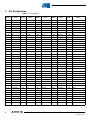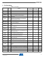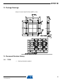
1
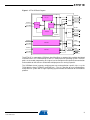
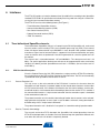
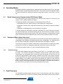
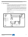
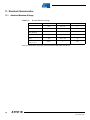
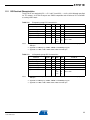
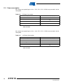
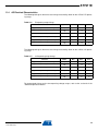
Features
• Also known as SMCS332SpW
• 3 identical bidirectional SpaceWire links allowing
•
•
•
•
•
•
•
•
•
•
•
•
•
•
– full duplex communication
– transmit rate from 1.25 up to 200 Mbit/s in each direction
Derived from the TSS901E-SMCS332 triple IEEE 1355 high speed controller
– Known anomalies of the TSS901E chip corrected
– Slightly different startup behavior
COmmunication Memory Interface (COMI)
– autonomous accesses to a communication memory
HOst Control Interface (HOCI)
– gives read/write accesses to the AT7911E configuration registers
– gives read/write accesses to the SpaceWire channels
Arbitration unit
– Allows two AT7911E to share one Dual Port RAM without external arbitration
Scalable databus width
– 8/16/32 bit width available
– allows flexible integration with any CPU type
Allows Little endian and Big endian configuration
Performance
– At 3.3V: 100 Mbit/s full duplex communication in each direction
– At 5V: 200 Mbit/s full duplex communication in each direction
Operating range
– Voltages
• 3V to 3.6V
• 4.5V to 5.5V
– Temperature
• - 55°C to +125°C
Maximum Power consumption
– At 3.6V with a 15MHz clock : 0.4 W
– At 5.5V with a 25 MHz clock : 1.7 W
Radiation Performance
– Total dose tested successfully up to 50 Krad (Si)
– No single event latchup below a LET of 80 MeV/mg/cm2
ESD better than 2000V
Quality Grades :
– QML-Q or V with SMD
Package : 196 pins MQFPL
Mass : 12grams
Triple
SpaceWire links
High Speed
Controller
AT7911E
1. Description
The AT7911E provides an interface between three SpaceWire links according to the SpaceWire
standard ECSS-E-50-12A specification and a data processing node consisting of a Control Processing Unit and a communication data memory.
The AT7911E was designed by EADS Astrium in Germany under the name 'SMCS332SpW" for
"Scalable Multi-channel Communication Subsystem for SpaceWire". It is manufactured using
the SEU hardened cell library from Atmel MG2RT CMOS 0.5µm radiation tolerant sea of gates
technology.
For any technical question relative to the functionality of the AT7911E please contact Atmel
technical support at [email protected].
This document shall be read in conjunction with EADS Astrium 'SMCS332SpW User Manual'.
The complete user manual of the AT7911E also called SMCS332SpW is available at
www.atmel.com.
The AT7911E provides hardware supported execution of the major parts of the interprocessor
communication protocol, particularly:
•
Transfer of data between two nodes of a multi-processor system with minimal host CPU
intervention
•
Execution of simple commands to provide basic features for system control functions
•
Provision of fault tolerant features.
Target applications are heterogeneous multi-processor systems supported by scalable interfaces including the little/big endian byte swapping. The AT7911E connects modules with
different processors (e.g. TSC695F, AT697E and others). Any kind of network topology could be
realized through the high speed point-to-point SpaceWire links (see the section ‘Applications’).
It can also be used for modules without any communication features such as special image compression chips, some signal processors, application specific programmable logic or mass
memory.
The AT7911E may also be used in single board systems where standardised high speed interfaces are needed and systems containing "non-intelligent" modules such as A/D-converter or
sensor interfaces which can be assembled with the AT7911E thanks to the "control by link"
feature.
2
AT7911E
7737B–AERO–05/08
AT7911E
Figure 1. AT7911E Block Diagram
CMADR
Receive
CM_CONTROL
COMI
CMDATA
D/S RCV 1
D/S TRM 1
SpaceWire
Protocol
HADR
H_CONTROL
Transmit
HOCI
Channel1
HINTR
D/S RCV 2
D/S TRM 2
HDATA
CPUR
Channel2
PRCI
SES
D/S RCV 3
Channel3
D/S TRM 3
JTAG
TEST
CLOCK
RESET
The AT7911E is supported by VSPWorks from Wind River, a commercially available distributed
real-time kernel. It is a multi-tasking as well as a multi-processor Operating System. The main
goals are to enable programming at a higher level to configure and to perform communication
and to administer the tasks on a board with multiple processes running in parallel.
The VSPWorks kernel supports multiple processors and application specific chips, e.g. the
TSC21020, the Sparc TSC695F, the AT697 etc.... Thus it is possible to run a heterogeneous
multiprocessor system with a single Operating System without consideration of the hardware
platform.
3
7737B–AERO–05/08
2. Pin Configuration
Table 1. Pin assignment
Pin
Name
Number
4
Pin
Number
Name
Pin
Name
Number
Pin
Name
Number
Pin
Name
Number
1
PLLOUT
41
VCC
81
HDATA28
121
CMDATA0
161
GND
2
GND
42
GND
82
HDATA29
122
CMDATA1
162
CMDATA27
3
VCC
43
HDATA0
83
VCC
123
CMDATA2
163
CMDATA28
4
CLK
44
HDATA1
84
GND
124
VCC
164
CMDATA29
5
RESET*
45
HDATA2
85
HDATA30
125
GND
165
CMDATA30
6
CLK10
46
HDATA3
86
HDATA31
126
CMDATA3
166
CMDATA31
7
HOSTBIGE
47
HDATA4
87
CPUR*
127
CMDATA4
167
GND
8
TCK
48
HDATA5
88
SES0*
128
CMDATA5
168
GND
9
TMS
49
HDATA6
89
SES1*
129
VCC
169
VCC_3VOLT
10
TDI
50
VCC
90
SES2*
130
GND
170
GND
11
TRST*
51
GND
91
SES3*
131
CMDATA6
171
GND
12
TDO
52
HDATA7
92
CAM
132
CMDATA7
172
VCC
13
VCC
53
HDATA8
93
COCI
133
CMDATA8
173
GND
14
GND
54
HDATA9
94
COCO
134
VCC
174
GND
15
HSEL*
55
HDATA10
95
CMCS0*
135
GND
175
NC
16
HRD*
56
HDATA11
96
CMCS1*
136
CMDATA9
176
LDI1
17
HWR*
57
VCC
97
VCC
137
CMDATA10
177
LSI1
18
HACK
58
GND
98
GND
138
CMDATA11
178
LDO1
19
HINTR*
59
HDATA12
99
CMRD*
139
CMDATA12
179
LSO1
20
VCC
60
HDATA13
100
CMWR*
140
CMDATA13
180
LDI2
21
GND
61
HDATA14
101
CMADR0
141
CMDATA14
181
LSI2
22
HADR0
62
HDATA15
102
CMADR1
142
VCC
182
NC
23
HADR1
63
HDATA16
103
CMADR2
143
GND
183
VCC
24
HADR2
64
HDATA17
104
CMADR3
144
CMDATA15
184
VCC
25
HADR3
65
VCC
105
CMADR4
145
CMDATA16
185
VCC
26
HADR4
66
GND
106
VCC
146
CMDATA17
186
LDO2
27
HADR5
67
HDATA18
107
GND
147
CMDATA18
187
LSO2
28
HADR6
68
HDATA19
108
CMADR5
148
CMDATA19
188
LDI3
29
HADR7
69
HDATA20
109
CMADR6
149
CMDATA20
189
LSI3
30
VCC
70
HDATA21
110
CMADR7
150
VCC
190
LDO3
31
GND
71
HDATA22
111
CMADR8
151
GND
191
LSO3
32
BOOTLINK
72
HDATA23
112
CMADR9
152
CMDATA21
192
TIME_CODE_SYNC
33
SCMSADR0
73
VCC
113
CMADR10
153
CMDATA22
193
GND
34
SMCSADR1
74
GND
114
CMADR11
154
CMDATA23
194
GND
35
SMCSADR2
75
HDATA24
115
VCC
155
VCC
195
VCC
36
SMCSADR3
76
HDATA25
116
GND
156
GND
196
GND
37
SMCSID0
77
HDATA26
117
CMADR12
157
CMDATA24
38
SMCSID1
78
VCC
118
CMADR13
158
CMDATA25
39
SMCSID2
79
GND
119
CMADR14
159
CMDATA26
40
SMCSID3
80
HDATA27
120
CMADR15
160
VCC
AT7911E
7737B–AERO–05/08
AT7911E
3. Pin Description
Table 2. Pin description
Signal Name(1)(3)
Type(2)(4)
Function
5V ± 0.5V
3.3V ± 0.3V
max. output
max. output
current [mA]
current [mA]
load [pF]
HSEL*
I
Select host interface
HRD*
I
host interface read strobe
HWR*
I
host interface write strobe
HADR(7:0)
I
AT7911E register address lines. These address lines will be
used to access (address) the AT7911E registers.
HDATA(31:0)
IO/Z
AT7911E data
3
1.5
50
HACK
O/Z
host acknowledge. The AT7911E deasserts this output to
add waitstates to an AT7911E access. After AT7911E is
ready this output will be asserted.
3
1.5
50
HINTR*
O/Z
host interrupt request line
3
1.5
50
SMCSADR(3:0 )
I
Address. The binary value of these lines will be compared
with the value of the ID lines.
SMCSID(3:0)
I
ID lines: offers possibility to use sixteen AT7911E within one
HSEL*
HOSTBIGE
I
BOOTLINK
I
CMCS(1:0)*
O/Z
Communication memory select lines. These pins are
asserted as chip selects for the corresponding banks of the
communication memory.
6
3
25
CMRD*
O/Z
Communication memory read strobe. This pin is asserted
when the AT7911E reads data from memory.
6
3
25
CMWR*
O/Z
Communication memory write strobe. This pin is asserted
when the AT7911E writes to data memory.
6
3
25
CMADR(15:0)
O/Z
Communication memory address. The AT7911E outputs an
address on these pins.
6
3
25
CMDATA(31:0)
IOZ
Communication memory data. The AT7911E inputs and
outputs data from and to com. memory on these pins.
3
1.5
25
COCI
I
Communication interface 'occupied' input signal
COCO
O
Communication interface 'occupied' output signal
3
1.5
50
CAM
I
Communication interface arbitration master input signal
1: master
0: slave
CPUR*
O
CPU Reset Signal (can be used as user defined flag)
3
1.5
50
SES(3:0)*
O
Specific External Signals (can be used as user defined flags)
3
1.5
50
LDI1
I
Link Data Input channel 1
LSI1
I
Link Strobe Input channel 1
LDO1
O
Link Data Output channel 1
12
6
25
0: host I/F Little Endian
1: host I/F Big Endian
0: control by host
1: control by link
5
7737B–AERO–05/08
Signal Name(1)(3)
Type(2)(4)
Function
5V ± 0.5V
3.3V ± 0.3V
max. output
max. output
current [mA]
current [mA]
12
6
25
load [pF]
LSO1
O
Link Strobe Output channel 1
LDI2
I
Link Data Input channel 2
LSI2
I
Link Strobe Input channel 2
LDO2
O
Link Data Output channel 2
12
6
25
LSO2
O
Link Strobe Output channel 2
12
6
25
LDI3
I
Link Data Input channel 3
LSI3
I
Link Strobe Input channel 3
LDO3
O
Link Data Output channel 3
12
6
25
LSO3
O
Link Strobe Output channel 3
12
6
25
TRST*
I
Test Reset. Resets the test state machine.
TCK
I
Test Clock. Provides an asynchronous clock for JTAG
boundary scan.
TMS
I
Test Mode Select. Used to control the test state machine.
TDI
I
Test Data Input. Provides serial data for the boundary scan
logic.
TDO
O
Test Data Output. Serial scan output of the boundary scan
path.
3
1.5
50
RESET*
I
Reset. Sets the AT7911E to a known state. This input must
be asserted (low) at power-up. The minimum width of
RESET low is 5 cycles of CLK10 in parallel with CLK
running.
CLK
I
CLK10
I
External clock input to AT7911E DS-links (application
specific, nominal 10 MHz). Used to generate to transmission
speed and link disconnect timeout.
I
A falling edge on this signal sends (if enabled) the internal
SpaceWire time code value over the links
PLLOUT
O
Output of internal PLL. Used to connect a network of
external RC devices. This is not a PLL clock output.
VCC_3VOLT
I
TIME_CODE_SY
NC
External clock input to AT7911E (max. 25 MHz).
Must be derived from RAM access time.
PLL Control signal - Configure PLL for 3.3V or 5V operation
VCC = 5 Volt: connect this signal with GND
VCC = 3.3 Volt: connect this signal with VCC
VCC
Power Supply
GND
Ground
Notes:
1. Groups of pins represent busses where the highest number is the MSB.
2. O = Output; I = Input; Z = High Impedance
3. (*) = active low signal
4. O/Z = if using a configuration with two AT7911Es these signals can directly be connected
together (WIROR)
6
AT7911E
7737B–AERO–05/08
AT7911E
4. Interfaces
The AT7911E provides an interface between three SpaceWire links according to the SpaceWire
standard ECSS-E-50-12A specification and a data processing node consisting of a Central Processing Unit and a communication data memory.
The AT7911E consists of the following blocks (See Figure 1):
• Three bidirectional SpaceWire channels
• Communication Memory Interface (COMI)
• Host Control Interface (HOCI)
• Protocol Command Interface (PRCI)
• JTAG Test Interface
4.1
Three bidirectional SpaceWire channels,
Three bidirectional SpaceWire channels, all comprising the DS-link SpaceWire cell, receive and
transmit sections (each including FIFOs) and a protocol processing unit (PPU). Each channel
allows full duplex communication up to 200 Mbit/s in each direction. With protocol command
execution a higher level of communication is supported. Link disconnect detection and parity
check at character level are performed. A checksum generation for a check at packet level can
be enabled.
The transmit rate is selectable between 1.25 and 200 Mbit/s. The startup transmit rate is 10
Mbit/s. For special applications the data transmit rate can be programmed to values even below
10 Mbit/s; the lowest possible SpaceWire transmit rate is 1.25 Mbit/s (the next values are 2.5
and 5 Mbit/s).
4.1.1
PPU Functional Description
Since the Protocol Processing Unit (PPU) determines a major part of the AT7911E functionality,
the principal blocks of the PPU and their function are described here. The PPU unit functionality
is provided for each SpaceWire channel of the AT7911E.
4.1.1.1
Protocol Execution Unit
This unit serves as the main controller of the PPU block. It receives the character from the
SpaceWire cell and interprets (in protocol mode) the four header data characters received after
an EOP control character. If the address field matches the link channel address and the command field contains a valid command then forwarding of data into the receive FIFO is enabled. If
the command field contains a "simple control command" then the execution request is forwarded
to the command execution unit.
The protocol execution unit also enables forwarding of header data characters to the acknowledge generator and provides an error signal in case of address mismatch, wrong commands or
disabled safety critical "simple control commands".
The protocol execution unit is disabled in "transparent" or “wormhole routing” operation mode.
4.1.1.2
Receive, Transmit, Acknowledge
The transmit and receive FIFOs decouple the SpaceWire link related operations from the
AT7911E related operations in all modes and such allows to keep the speed of the different units
even when the source or sink of data is temporarily blocked.
7
7737B–AERO–05/08
In the protocol mode an additional FIFO (acknowledge FIFO) is used to decouple sending of
acknowledges from receiving new data when the transmit path is currently occupied by a running packet transmission.
4.1.1.3
Command Execution Unit
This unit performs activating resp. deactivating of the CPU reset and the specific external signals and provides the capability to reset one or all links inside the AT7911E, all actions
requested by the decoded commands from the protocol execution unit.
The unit contains a register controlling the enable/disable state of safety critical commands
which is set into the 'enable' state upon command request and which is reset after a safety critical command has been executed.
The CPU reset and the specific external signals are forwarded to the Protocol Command Interface (PRCI).
4.2
Communication Memory Interface (COMI)
The COMI performs autonomous accesses to the communication memory of the module to store
data received via the links or to read data to be transmitted via the links. The COMI consists of
individual memory address generators for the receive and transmit direction of every SpaceWire
link channel. The access to the memory is controlled via an arbitration unit providing a fair arbitration scheme. Two AT7911E can share one DPRAM without external arbitration logic.
The data bus width is scalable (8/16/32 bit) to allow flexible integration with any CPU type.
Operation in little or big endian mode is configurable through internal registers.
The COMI address bus is 16 bit wide allowing direct access of up to 64K words (32 bits) of the
DPRAM. Two chip select signals are provided to allow splitting of the 64k address space in two
memory banks.
4.3
Host Control Interface (HOCI)
The HOCI gives read and write access to the AT7911E configuration registers and to the
SpaceWire channels for the controlling CPU. Viewed from the CPU, the interface behaves like a
peripheral that generates acknowledges to synchronize the data transfers and which is located
somewhere in the CPU's address space.
Packets can be transmitted or received directly via the HOCI. In this case the Communication
Memory (DPRAM) is not strictly needed. However, in this case the packet size should be limited
to avoid frequent CPU interaction.
The data bus width is scalable (8/16/32 bit) to allow flexible integration with any CPU type. The
byte alignment can be configured for little or big endian mode through an external pin.
Additionally, the HOCI contains the interrupt signalling capability of the AT7911E by providing an
interrupt output, the interrupt status register and interrupt mask register to the local CPU.
A special pin is provided to select between control of the AT7911E by HOCI or by link. If control
by link is enabled, the host data bus functions as a 32-bit general purpose interface (GPIO).
4.4
Protocol Command Interface (PRCI)
The PRCI collects the decoded commands from all PPUs and forwards them to external circuitry
via 5 special pins.
8
AT7911E
7737B–AERO–05/08
AT7911E
4.5
JTAG Test Interface
It represents the boundary scan testing provisions specified by IEEE Standard 1149.1 of the
Joint Testing Action Group (JTAG). The AT7911E test access port and on-chip circuitry is fully
compliant with the IEEE 1149.1 specification. The test access port enables boundary scan testing of circuitry connected to the AT7911E I/O pins.
9
7737B–AERO–05/08
5. Control Interface
The AT7911E can be configured/controled through two interfaces:
• HOCI interface
• Link control interface
5.1
HOCI interface
The HOst Control Interface is especialy designed for access to internal AT6911E registers by a
local controller (µController, FPGA etc.).
The detailed description of this operation mode can be found in the section 5.4 of the
'SMCS332SpW User Manual'.
5.2
Link control interface
Link control is the feature of the AT7911E that allows the control of the AT7911E not only via
HOCI but via one of the three links. This allows to use the AT7911E in systems without a local
controller. Since the HOCI is no longer used in this operation mode, it is instead available as a
set of general purpose I/O (GPIO) lines.
The detailed description of this operation mode can be found in the section 5.4 of the
'SMCS332SpW User Manual'.
10
AT7911E
7737B–AERO–05/08
AT7911E
6. Operating Modes
According to the different protocol formats expected for the operation of the AT7911E, two major
operation modes are implemented into the AT7911E. For each link channel the operation modes
are chosen individually by setting the respective configuration registers via the HOCI or via the
link.
6.1
Simple Interprocessor Communication (SIC) Protocol Mode
This mode executes the simple interprocessor communication protocol as described in the
chapter 13 of the 'SMCS332SpW User Manual'.
The following capabilities of the protocol are implemented into the AT7911E:
• Interpretation of the first 4 data characters as the header bytes of the protocol
• Autonomous execution of the simple control commands as described in the above mentioned
chapter
• Autonomous acknowledgement of received packets if configured
In transmit direction no interpretation of the data is performed. This means that for transmit packets, the four header bytes must be generated by the host CPU and must be available as the first
data read from the communication memory. EOP control characters are automatically inserted
by the AT7911E when one configured transfer from the communication memory has finished.
6.2
Transparent Mode (default after reset)
This mode allows complete transparent data transfer between two nodes without performing any
interpretation of the databytes and without generating any acknowledges. It is completely up to
the host CPU to interpret the received data and to generate acknowledges if required.
The AT7911E accepts EOP and EEP control tokens as packet delimiters and generates autonomously EOP or no EOP (as configured) marker after each end of a transmission packet.
The transparent mode includes as a special submode: Wormhole routing.
6.2.1
Wormhole routing
This mode allows hardware routing of packets by the AT7911E. It is a submode of the transparent mode. The AT7911E introduces a wormhole routing function similar to the routing
implemented in the SpaceWire router. Each of the three links and the AT7911E itself can be
assigned an eight bit address. When routing is enabled in the AT7911E, the first byte of a packet
will be interpreted as the address destination byte, analysed and removed from the packet
(header deletion). If this address matches one of the two other link addresses or the AT7911E
address assigned previously, the packet will be automatically forwarded to this link or the FIFO
of the AT7911E. If the header byte does not match a link address, the packet will be written to
the internal FIFO as well and an error interrupt (maskable) will be raised.
7. Fault Tolerance
The SpaceWire standard specifies low level checks as link disconnect, credit value, sequence
and parity at token level. The AT7911E provides, through the Protocol Processing Unit, features
11
7737B–AERO–05/08
to reset a link or all links inside the AT7911E, to reset the local CPU or to send special signals to
the CPU commanded via the links.
Additionally it is possible to enable a checksum coder/decoder to have fault detection capabilities at packet level.
12
AT7911E
7737B–AERO–05/08
AT7911E
8. Typical Applications
The AT7911E can be used for single board systems where standardised high speed interfaces
are needed. Even "non-intelligent" modules such as A/D-converter or sensor interfaces can be
assembled with the AT7911E because of the "control by link" feature. The complete control of
the AT7911E can be done via link from a central controller-node.
The AT7911E is a very high speed, scalable link-interface chip with fault tolerance features. The
initial exploitation is for use in multi-processor systems where the standardization or the high
speed of the links is an important issue and where reliability is a requirement. Further application
examples are heterogeneous systems or modules without any communication features as special image compression chips, certain signal processors, application specific programmable
logic or mass memory.
The Figure below shows the AT7911E (also called SMCS332SpW) embedded in a typical module environment:
Figure 8-1.
Typical Application
SMCS332SpW
Processor
HOSTBIGE
HINTR
INTERRUPT IN
BOOTLINK
HSEL
CHIP SELECTS
RESET
HRD
CLK
HWR
CLK10
HADR
SPACEWIRE LINK 1
WRITE
HACK
HDATA
4
READ
SMCSADR
WAIT/ACK
32
DATA
8
ADDRESS
4
4
SMCSID
ID
4
SPACEWIRE LINK 2
CPUR
4
SES
4
SPACEWIRE LINK 3
TIME_CODE_SYNC
CMCS0
SELECT A
CMCS1
SELECT
OE A A
CMRD
CMWR
CMDATA
OE
WEAA
32
16
CMADR
VCC
COCO
JTAG
OE
WEBB
WE
DATA
A A
DATA
WE BB
DATA
ADDRAA
DATA
ADDRBB
ADDR A
CAM
5
SELECT B
SELECT
OEBB
COCI
ADDR B
Dual Port
Communication
Dual Port
Memory
Communication
Memory
BANK 0
BANK 1
GND
PLLOUT
13
7737B–AERO–05/08
8.1
AT7911E connected with the TSS901E (or SMCS332)
The new ECSS-E-50-12A SpaceWire standard, used by the AT7911E and the IEEE-1355 standard used by the old TSS901E are compatible, however the TSS901E has a slightly different
startup behavior, the TSS901E must be started first on a link connecting with the AT7911E.
8.2
AT7911E differences with the TSS901E (or SMCS332)
A few differences between the AT7911E and the TSS901E exist in the registers and in the
pinout. These differences are detailed in the section 14 of the ‘SMCS332SpW User Manual”.
8.3
Handling empty packets
An anomaly due to the SpaceWire codec implemented in the AT7911E affect the behavior of the
AT7911E when receiving empty packets. The description of this anomaly and the possible
workaround are given in the section 12 of the ‘SMCS332SpW User Manual”.
14
AT7911E
7737B–AERO–05/08
AT7911E
9. PLL Filter
The AT7911E embeds a PLL to generate its internal clock reference. The PLLOUT pin of the
PLL is the output of the AT7911E that allows connection of the external filter of the PLL. The following figure presents the connection of the PLL filter.
Figure 9-1.
PLL filter
AT7911E
Table 9-1.
PLL filter recommended components
VCC = +5V ± 0.5V
VCC = +3.3V ± 0.3V
R1
1,8 kΩ ± 5%, ¼W
R1
2,0 kΩ ± 5%, ¼W
C1
33pF, ± 5%
C1
33pF, ± 5%
C2
820pF, ± 5%
C2
760pF, ± 5%
10. Power Supply
To achieve its fast cycle time, the AT7911E is designed with high speed drivers on output pins.
Large peak currents may pass through a circuit board’s ground and power lines, especially when
many output drivers are simultaneously charging or discharging their load capacitances. These
transient currents can cause disturbances on the power and ground lines. To minimize these
effects, the AT7911E provides separate supply pins for its internal logic and for its external
drivers.
All GND pins should have a low impedance path to ground. A ground plane is required in
AT7911E systems to reduce this impedance, minimizing noise.
The VCC pins should be bypassed to the ground plane using approximately 10 high-frequency
capacitors (0.1 F ceramic). Keep each capacitor’s lead and trace length to the pins as short as
possible. This low inductive path provides the AT7911E with the peak currents required when its
output drivers switch. The capacitors’ ground leads should also be short and connect directly to
the ground plane. This provides a low impedance return path for the load capacitance of the
AT7911E output drivers.
The following pins must have a capacitor: 20, 78, 129, and 155. The remaining capacitors
should be distributed equally around the AT7911E.
15
7737B–AERO–05/08
11. Electrical Characteristics
11.1
Absolute Maximum Ratings
Table 11-1.
Absolute Maximum Ratings
Parameter
Supply Voltage
Symbol
Value
Unit
VCC
-0.5 to +7
V
-0.5 to VCC + 0.5
V
I/O Voltage
Operating Temperature
Range (Ambient)
TA
-55 to +125
°C
Junction Temperature
TJ
TJ < TA +20
°C
Storage Temperature
Range
Tstg
-65 to +150
°C
RThJC
4
°C/W
Thermal resistance:
junction to case
Stresses above those listed may cause permanent damage to the device.
16
AT7911E
7737B–AERO–05/08
AT7911E
11.2
DC Electrical Characteristics
The AT7911E can work with VCC = + 5 V ± 0.5 V and VCC = + 3.3V ± 0.3V. Although specified
for TTL outputs, all AT7911E outputs are CMOS compatible and will drive to VCC and GND
assuming no DC loads.
Table 11-2.
5V operating range DC Characteristics.
Parameter
Symbol
Min.
Operating Voltage
VCC
4.5
Input HIGH Voltage
VIH
2.2
Input LOW Voltage
VIL
Output HIGH Voltage
VOH
Max.
5.5
Conditions
V
V
0.8
V
2.4
V
IOL = 3, 6, 12mA / VCC = VCC(min)
Output LOW Voltage
VOL
0.4
V
IOH = 3, 6, 12mA / VCC = VCC(min)
Output Short circuit current
IOS
90(1)
mA
mA
mA
VOUT = VCC
VOUT = GND
180(2)
270(3)
Notes:
Unit
1. Applicable for HDATA[31:0], HACK, HINTR*, CMDATA[31:0], COCI, CPUR*, SES[3:0]* and
TDO pins
2. Applicable for CMCS[1:0]*, CMRD*, CMWR* and CMADR[31:0] pins
3. Applicable for LDO1, LSO1, LDO2, LSO2, LDO3 and LSO3 pins
Table 11-3.
3.3V operating range DC Characteristics.
Parameter
Symbol
Min.
Operating Voltage
VCC
3.0
Input HIGH Voltage
VIH
2.0
Input LOW Voltage
VIL
Output HIGH Voltage
VOH
Output LOW Voltage
VOL
Output Short circuit current
IOS
Max.
3.6
Conditions
V
V
0.8
V
2.4
0.4
50
(1)
(2)
100
155(3)
Notes:
Unit
V
IOL = 1.5, 3, 6mA / VCC = VCC(min)
V
IOH = 1, 2, 4mA / VCC = VCC(min)
mA
mA
mA
VOUT = VCC
VOUT = GND
1. Applicable for HDATA[31:0], HACK, HINTR*, CMDATA[31:0], COCI, CPUR*, SES[3:0]* and
TDO pins
2. Applicable for CMCS[1:0]*, CMRD*, CMWR* and CMADR[31:0] pins
3. Applicable for LDO1, LSO1, LDO2, LSO2, LDO3 and LSO3 pins
17
7737B–AERO–05/08
11.3
Power consumption
Max. power consumption figures at Vcc = 5.5V; -55°C; CLK = 25 MHz are presented in the following table.
Table 11-4.
5V Power Consumption
Operation Mode
not clocked
8
AT7911E in RESET
AT7911E in IDLE
(1)
Maximum
1.
Power consumption [mA]
75
115
310
IDLE means clk = 25 MHz, all three links started and running at 10Mbit/s, no activity on
HOCI and COMI
Max. power consumption figures at Vcc = 3.6V; -55°C; CLK = 15 MHz are presented in the following table.
Table 11-5.
3.3V Power Consumption
Operation Mode
not clocked
4
AT7911E in RESET
24
(1)
38
AT7911E in IDLE
Maximum
1.
18
Power consumption [mA]
100
IDLE means clk = 15 MHz, all three links started and running at 10Mbit/s, no activity on
HOCI and COMI
AT7911E
7737B–AERO–05/08
AT7911E
11.4
AC Electrical Characteristics
The following table gives the worst case timings measured by Atmel on the 4.5V to 5.5V operating range
Table 11-6.
5V operating range timings.
Parameter
Symbol
Min.
Max.
Unit
Propagation delay CLK Low to HACK High
Tp1
29
ns
Propagation delay CLK High to CMCS0* Low
Tp2
18
ns
Propagation delay CLK High to CMADR0 High
Tp3
17
ns
Propagation delay CLK10 High to LDO1 High
Tp4
30
ns
Propagation delay CLK10 High to LDO2 High
Tp5
32
ns
Propagation delay CLK10 High to LDO3 High
Tp6
36
ns
The following table gives the worst case timings measured by Atmel on the 3.0V to 3.6V operating range
Table 11-7.
3.3V operating range timings
Parameter
Symbol
Min.
Max.
Unit
Propagation delay CLK Low to HACK High
Tp1
47
ns
Propagation delay CLK High to CMCS0* Low
Tp2
30
ns
Propagation delay CLK High to CMADR0 High
Tp3
28
ns
Propagation delay CLK10 High to LDO1 High
Tp4
51
ns
Propagation delay CLK10 High to LDO2 High
Tp5
54
ns
Propagation delay CLK10 High to LDO3 High
Tp6
61
ns
For guaranteed timings on the two operating voltage ranges, refer to the section 9 of the
‘SMCS332SpW User Manual’
19
7737B–AERO–05/08
12. Ordering Information
Part-number
Temperature Range
Package
Quality Flow
AT7911EFA-E
25°C
MQFPL196
Engineering sample
5962-08A0101QXC
-55°C to +125°C
MQFPL196
Mil Level B (*)
5962-08A0101VXC
-55°C to +125°C
MQFPL196
Space Level B (*)
(*) according to Atmel Quality flow document 4288, see Atmel web site.
20
AT7911E
7737B–AERO–05/08
AT7911E
13. Package Drawings
196 pins Ceramic Quad Flat Pack (MQFP_L 196)
14. Document Revision History
14.1
7737B
1. Ordering information updated.
21
7737B–AERO–05/08
Headquarters
International
Atmel Corporation
2325 Orchard Parkway
San Jose, CA 95131
USA
Tel: 1(408) 441-0311
Fax: 1(408) 487-2600
Atmel Asia
Room 1219
Chinachem Golden Plaza
77 Mody Road Tsimshatsui
East Kowloon
Hong Kong
Tel: (852) 2721-9778
Fax: (852) 2722-1369
Atmel Europe
Le Krebs
8, Rue Jean-Pierre Timbaud
BP 309
78054 Saint-Quentin-enYvelines Cedex
France
Tel: (33) 1-30-60-70-00
Fax: (33) 1-30-60-71-11
Atmel Japan
9F, Tonetsu Shinkawa Bldg.
1-24-8 Shinkawa
Chuo-ku, Tokyo 104-0033
Japan
Tel: (81) 3-3523-3551
Fax: (81) 3-3523-7581
Technical Support
[email protected]
Sales Contact
www.atmel.com/contacts
Product Contact
Web Site
www.atmel.com
Literature Requests
www.atmel.com/literature
Disclaimer: The information in this document is provided in connection with Atmel products. No license, express or implied, by estoppel or otherwise, to any
intellectual property right is granted by this document or in connection with the sale of Atmel products. EXCEPT AS SET FORTH IN ATMEL’S TERMS AND CONDITIONS OF SALE LOCATED ON ATMEL’S WEB SITE, ATMEL ASSUMES NO LIABILITY WHATSOEVER AND DISCLAIMS ANY EXPRESS, IMPLIED OR STATUTORY
WARRANTY RELATING TO ITS PRODUCTS INCLUDING, BUT NOT LIMITED TO, THE IMPLIED WARRANTY OF MERCHANTABILITY, FITNESS FOR A PARTICULAR
PURPOSE, OR NON-INFRINGEMENT. IN NO EVENT SHALL ATMEL BE LIABLE FOR ANY DIRECT, INDIRECT, CONSEQUENTIAL, PUNITIVE, SPECIAL OR INCIDENTAL DAMAGES (INCLUDING, WITHOUT LIMITATION, DAMAGES FOR LOSS OF PROFITS, BUSINESS INTERRUPTION, OR LOSS OF INFORMATION) ARISING OUT
OF THE USE OR INABILITY TO USE THIS DOCUMENT, EVEN IF ATMEL HAS BEEN ADVISED OF THE POSSIBILITY OF SUCH DAMAGES. Atmel makes no
representations or warranties with respect to the accuracy or completeness of the contents of this document and reserves the right to make changes to specifications
and product descriptions at any time without notice. Atmel does not make any commitment to update the information contained herein. Unless specifically provided
otherwise, Atmel products are not suitable for, and shall not be used in, automotive applications. Atmel’s products are not intended, authorized, or warranted for use
as components in applications intended to support or sustain life.
© 2008 Atmel Corporation. All rights reserved. Atmel ®, logo and combinations thereof, and others are registered trademarks or trademarks of
Atmel Corporation or its subsidiaries. Other terms and product names may be trademarks of others.
7737B–AERO–05/08