1
4--4
Setup Programming
Step 2:
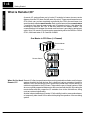
Write the Setup
Logic for Each
Remote Base
SP00
Remote #1
Input
SP00
Remote #1
Output
SP00
Remote I/O
Setup Programming
Remote #2
Input
SP00
Remote #2
Output
SP00
Remote #3
Input
SP00
Remote #3
Output
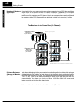
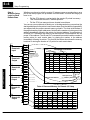
Whether you choose to write the remote I/O setup program as a subroutine or as a
part of the main program, the procedure is still the same. You have two things you
have to do:
S Tell the CPU where to read and write the remote I/O points in memory.
This is done with the use of “address pointers”.
S Tell the CPU how many points are located in each base.
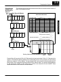
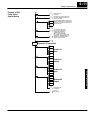
You can use your worksheets to assist you. In the diagram below, you see how the
starting addresses for the points in each remote base (from the tables in Appendix B)
are mapped with the proper reserved memory pointers. The chart at the bottom of
the page shows the pointer addresses. Notice that the number of points goes in the
address immediately following the pointer for the start address. A combination of
LDA and OUT commands are used to load and map the V40xxx address into the
proper V74xx address. The LD and OUT commands are used to load the number of
remote points for each remote base, by placing the number in the address
immediately following its pointer. The chart at the bottom also shows the memory
locations for storing the number of I/O points for each remote base.
LDA
O40403
OUT
V7404
LD
K16
OUT
V7405
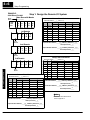
Remote Slave Worksheet
1
Note:
Remote Base Address_________(Choose 1--7)
The LDA instruction is
loading octal numbers
and therefor a capital O
is placed in front of the
number
INPUT
OUTPUT
Slot
Number
Module
Name
Input Address
0
08ND3S
X060
8
LD
K16
1
08ND3S
X070
8
2
OUT
V7407
3
LDA
O40502
OUT
V7406
LDA
O40404
4
OUT
V7410
5
Starting Address
OUT
V7412
Pointer Address
8
Y050
8
16
Total Input Points_____
Y040
40502
Output Bit Start Address:________V-Memory
Address:V_______
No. of I/O Points
16
Total Output Points_____
Pointer Address + 1
LDA
O40406
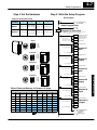
Table of Reserved Memory for Remote I/O Setup
OUT
V7414
LD
Y040
08TD1
X060
40403
Input Bit Start Address:________V-Memory
Address:V_______
LDA
O40503
K32
08TD1
7
OUT
V7411
OUT
V7413
No.Outputs
6
LD
K32
LD
Output Address
No. Inputs
First Master Module
K16
Second Master Module
OUT
V7415
Slave
LDA
O40505
Input
Address
Number of
Input Pts
Output
Address
Number of
Output Pts
Input
Address
1
V7404
V7405
V7406
V7407
V7444
V7445
V7446
V7447
2
V7410
V7411
V7412
V7413
V7450
V7451
V7452
V7453
3
V7414
V7415
V7416
V7417
V7454
V7455
V7456
V7457
4
V7420
V7421
V7422
V7423
V7460
V7461
V7462
V7463
OUT
V7416
LD
K16
OUT
V7417
Number of Output
Input Pts Address
Number of
Output Pts
5
V7424
V7425
V7426
V7427
V7464
V7465
V7466
V7467
6
V7430
V7431
V7432
V7433
V7470
V7471
V7472
V7473
7
V7434
V7435
V7436
V7437
V7474
V7475
V7476
V7477