1
MAXQ615
16-Bit MAXQ Microcontroller with
Hardware Multiplier
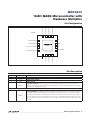
ABSOLUTE MAXIMUM RATINGS
(All voltages relative to GND.)
Voltage Range on VDD..........................................-0.3V to +3.6V
Voltage Range on Any Lead..................... -0.3V to (VDD + 0.5V)
Continuous Output Current
Any Single I/O Pin...........................................................32mA
All I/O Pins Combined......................................................32mA
Continuous Power Dissipation (TA = +70NC)
TQFN (derate 16.9mW/NC above +70NC)..................1349mW
Operating Temperature Range .......................... -40NC to +85NC
Storage Temperature Range ........................... -65NC to +150NC
Lead Temperature (soldering, 10s)………………............+300NC
Soldering Temperature (reflow)……..………………….....+260NC
Stresses beyond those listed under “Absolute Maximum Ratings” may cause permanent damage to the device. These are stress ratings only, and functional operation of the device at these or any other conditions beyond those indicated in the operational sections of the specifications is not implied. Exposure to absolute
maximum rating conditions for extended periods may affect device reliability.
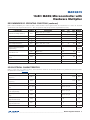
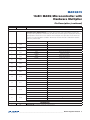
RECOMMENDED DC OPERATING CONDITIONS
(VDD = VRST to VDD(MAX), TA = -40NC to +85NC, unless otherwise noted. Typical values are measured at TA = +25NC. AC electrical
specifications and all specifications to TA = -40NC are guaranteed by design and are not production tested.)
PARAMETER
Supply Voltage
1.8V Internal Regulator
Power-Fail Warning Voltage
SYMBOL
CONDITIONS
MIN
TYP
MAX
UNITS
VDD
VRST
3.6
V
VREG18
1.62
1.7
1.98
V
VPFW
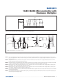
Monitors VDD (Notes 1, 2)
2.45
2.6
2.75
V
Power-Fail Reset Voltage
VRST
Monitors VDD (Note 3)
2.35
2.4
2.45
V
Power-On Reset Voltage
VPOR
Monitors VDD
1.0
1.45
V
Supply Current
IDD1
fCK = 20MHz (Note 4)
Idle Current
IIDLE
(Note 5)
ISTOP1
PF Off
Stop Mode Current
ISTOP2
PF On
Stop Mode Resume Time
Power-Fail Monitor Startup Time
Power-Fail Warning Detection
Time
2.6
4.5
mA
750
850
FA
0.3
3.0
TA = 0NC to +70NC
1
12
TA = -40NC to +85NC
2
16
TA = +25NC
22.0
35.0
TA = 0NC to +70NC
22.0
42.0
TA = -40NC to +85NC
22.0
45
1.0
TA = +25NC
tON
tPFM_ON
300
(Note 6)
tPFW
FA
Fs
150
10
Fs
Fs
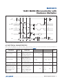
CLOCK SOURCE
Internal Ring Oscillator
Frequency
fCLK
±5%
20
45
MHz
Ring Oscillator Duty Cycle
tCLK_DUTY
55
%
System Clock Frequency
tCK
fCK
MHz
System Clock Period
fCK
1/fCK
ns
300
mV
DIGITAL I/O
Input Hysteresis
VIHYS
VDD = 3.3V, TA = +25NC
Input Low Voltage
VIL
VGND
Input High Voltage
VIH
0.7 x VDD
0.3 x VDD
VDD
V
V
����������������������������������������������������������������� Maxim Integrated Products 2