1
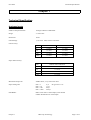
PCI - ADC
RoHS Compliant
PCI Multi-function
Analogue/Digital Interface Card
User Guide
Document Reference
Document Issue Level
Product User Guide
1.2
PCI-ADC
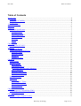
Table of Contents
Table of Contents
Introduction........................................................................................................................................ 4
Copyright.......................................................................................................................................4
Limitations of Liability................................................................................................................. 4
Trademarks.................................................................................................................................... 4
About The Manual............................................................................................................................. 5
Overview............................................................................................................................................ 6
Chapter 1............................................................................................................................................ 7
Technical Specification................................................................................................................. 7
Analogue Inputs........................................................................................................................7
Analogue Output.......................................................................................................................8
Digital Input/Output..................................................................................................................8
Counter/Timers......................................................................................................................... 8
Interrupts...................................................................................................................................9
Power........................................................................................................................................ 9
Physical.....................................................................................................................................9
Chapter 2.......................................................................................................................................... 10
Installing the PCI-ADC............................................................................................................... 10
Chapter 3.......................................................................................................................................... 11
Connection Details...................................................................................................................... 11
Suitable Interface Signal Types...................................................................................................12
Analogue Inputs......................................................................................................................12
Analogue Outputs................................................................................................................... 12
Digital I/O...............................................................................................................................13
Counter / Timers..................................................................................................................... 13
Chapter 4.......................................................................................................................................... 14
Address Map................................................................................................................................14
Analogue Inputs.......................................................................................................................... 15
FIFO Memory.........................................................................................................................16
Conversion Control.................................................................................................................16
Input Mode Selection and Calibration....................................................................................18
Auto-Calibration..................................................................................................................... 19
Analogue Input Status ............................................................................................................19
To Start A Conversion............................................................................................................ 20
Limitations to Use...................................................................................................................20
Analogue Outputs........................................................................................................................21
Digital I/O....................................................................................................................................23
i8255 PIO................................................................................................................................23
i8254 Counter / Timer............................................................................................................ 24
Counter / Timer Modes...........................................................................................................25
Counter Control...................................................................................................................... 26
Interrupt Selection.................................................................................................................. 27
Chapter 5.......................................................................................................................................... 29
Electromagnetic Compatibility (EMC)....................................................................................... 29
EMC Specification..................................................................................................................30
Chapter 6.......................................................................................................................................... 31
PCI-ADC Input / Output Circuitry.............................................................................................. 31
Blue Chip Technology
Page 2 of 33
PCI-ADC
Table of Contents
Amendment History......................................................................................................................... 32
Contact Details............................................................................................................................ 32
Blue Chip Technology
Page 3 of 33
PCI-ADC
Introduction
Introduction
Copyright
All rights reserved. No part of this publication may be reproduced, stored in any retrieval system, or transmitted, in
any form or by any means, electronic, mechanical, photocopied, recorded or otherwise, without the prior
permission, in writing, from the publisher. For permission in the UK please contact Blue Chip Technology.
Information offered in this manual is believed to be correct at the time of printing. Blue Chip Technology accepts
no responsibility for any inaccuracies. The information contained herein is subject to change without notice.
There are no express or implied licences granted herein to any intellectual property rights of Blue Chip Technology
Ltd.
Limitations of Liability
In no event shall Blue Chip Technology be held liable for any loss, expenses or damages of any kind whatsoever,
whether direct, indirect, incidental or consequential, arising from the design or use of this product or the support
materials supplied with this product. If this product proves to be defective, Blue Chip Technology is only obliged to
replace or refund the purchase price at Blue Chip Technology's discretion according to their Terms and Conditions
of Sale.
Trademarks
All trademarks and registered names acknowledged.
IBM, PC, AT and PS/2 are trademarks of International Business Machines Corporation (IBM).
AMI is a registered trademark of American Megatrends Inc.
MSDOS and WINDOWS are registered trademarks of the Microsoft Corporation.
Blue Chip Technology
Page 4 of 33
PCI-ADC
About The Manual
About The Manual
This manual is organised into six chapters. Each chapter covers a different aspect of using the
PCI-ADC. In order to get the best results from the product, the user is urged to read all chapters,
paying particular note to Chapter 2 which deals with the initial installation of the card.
Overview
Provides a brief introduction to the card
Chapter 1
Presents the card’s technical specification. Use this section to determine the card’s
suitability for a particular application
Chapter 2
Explains how to install the card in your computer.
Chapter 3
Details the connections to and from the card
Chapter 4
Gives details of the card’s address mapping and internal register details allowing
the user to write custom software to control the card.
Chapter 5
Electromagnetic Compatibility
Chapter 6
Timer Examples
This manual describes the complete hardware functionality of the PCI-ADC board. All the
functions may not necessarily be supported by the current release of the driver.
Page 5 of 33
PCI-ADC
Product Overview
Overview
The PCI-ADC is a RoHS-compliant PCI-compatible half-card which provides analogue and
digital input/outputs and counter/timers.
Eight differential or sixteen single ended analogue inputs are available with 12-bit resolution and
programmable gain to allow full scale input ranges of between ± 5mV and ± 5 volts. The
maximum sample rate of these is 230 Ksamples/s. A FIFO input buffer is available such that 1024
analogue samples may be taken before processor intervention is required.
Four bipolar analogue outputs are provided to 12 bits resolution. Each may be individually
configured as voltage or current outputs with full scale range of ±10 volts or ±20mA.
There are 24 TTL-compatible programmable digital input/outputs available from the board. If the
controlling devices are used in handshake mode, the handshake lines are available as interrupt
sources.
There are also three programmable counter/timers, the outputs of which may be used to generate
interrupts, to initiate analogue input conversion, analogue output sample update, or digital I/O. A
4 MHz crystal oscillator is available on board to allow the counter/timers to act as accurate
timebases.
All analogue and digital Input / Output lines are available at an industry standard 50 way D-type
plug connector.
One PCI interrupt line may be selectively driven by the eight interrupt sources on the board, the
interrupting source being readily identified by the board.
The PCI-ADC is intended to be installed with the minimum of user interaction. The board is
configured by the system BIOS and by the application drivers and
no on-board links are required to select functionality.
Blue Chip Technology
Page 6 of 33
PCI-ADC
Technical Specification
Chapter 1
Technical Specification
Analogue Inputs
Number Of Input Channels
16 Single ended or 8 differential
Range:
± 5 Volts max
Resolution:
12 bits
Gain Settings:
1, 10, 100 or 1000, software selectable
Gain accuracy:
Gain
With Auto Calibration Without Auto Calibration
x1
± 0.08%
± 0.10%
x10
± 0.12%
± 0.17%
x100
± 0.15%
± 0.32%
x1000
± 0.22%
± 0.32%
Input offset accuracy:
Gain
Without Auto Calibration
x1
± 0.10 %
x10
± 0.10 %
x100
± 0.10 %
x1000
± 0.12 %
Maximum sample rate:
230Ks/s burst, 4.3 µs conversion time
Input settling time
Gain = 1
Gain = 10
Gain = 100
Gain = 1000
Data Buffer:
FIFO 16 bits wide x 1024 samples, with channel
number identification on each sample
Chapter 1
9 µs
all typical to 0.1 %
11 µs
80 µs
600 µs
Blue Chip Technology
Page 7 of 33
PCI-ADC
Technical Specification
Analogue Output
Number of outputs
4
Output Resolution:
12 bits
Format:
Constant Voltage or Constant Current
Individually software selectable
Output levels:
Voltage mode = ± 10 volts
Current mode = ± 20 mA
Drive capability:
Voltage mode = ± 20 mA (full scale into 500R min)
Current mode = ± 12 volts (full scale into 600R max)
Accuracy:
Voltage mode = ± 0.35 %
Current mode = ± 0.50 %
Output slew rate:
0.05 V/µs
Digital Input/Output
Number of I/O channels
24 arranged as 3 x 8 I/O bits
Signal Levels:
5 Volt TTL Logic Levels
Outputs:
Logic low Level:
Logic High Level:
0 V (min) – 0.4 V (max) @ IOL = 2.5mA
3.5 V (min) – 5 V (max) @ IOH = -400 µA
Drive current:
2.5 mA (Logic Low) Vout = 0.4 Volts
-400 µA (Logic High) Vout = 3.5 Volts
Input Loading:
± 10 µA
Termination Resistors:
10K Resistor packs are fitted to each I/O port to pull the lines
to + 5 Volts. Optionally they may pull the lines down to 0 Volts
Counter/Timers
Counter/timers
3 x 16 bit. Counter/timers may be cascaded
On Board Oscillator:
Frequency 4 Mhz
Stability ± 100ppm 0 – 70 °C
Chapter 1
Blue Chip Technology
Page 8 of 33
PCI-ADC
Technical Specification
Interrupts
Interrupt Sources:
Register selectable to 3 Counter/timer outputs
2 PIO handshake control lines
ADC busy and FIFO Not Empty/Half Full
Levels Supported:
All PCI interrupts
Address overhead
26 I/O addresses in 3 PCI address spaces
Power
Board Power Requirement:
5W
This board requires both 5V and 3.3V power lines but can operate
with Vio of either 3.3V or 5V
Physical
Temperature:
Non Operating:
Operating:
-20 °C to 70 °C
0 °C to 70 °C
MTBF:
94,000 hours (Bellcore method)
Signal Connections:
1 x 50 way male “D-type” plug
Dimensions
165 (L) x 100 (H) board only
180 (L) x 122 (H) x 22 (W) including bracket
Chapter 1
Blue Chip Technology
Page 9 of 33
PCI-ADC
Installation
Chapter 2
Installing the PCI-ADC
The card is installed by removing the cover of the host computer and inserting the card into a free
PCI slot. The rear panel of the card should then be secured to the rear panel of the host computer
with the screw supplied with the computer.
When the computer is switched on, the BIOS will detect the presence of the card and will allocate
it with a base address and an interrupt. These parameters may then be used to configure
application software to access the card.
If the card is to be directly accessed by a user’s application, it will be necessary for the application
to determine where the BIOS has located the card.
One way of determining the Base address of the card can be found by using the “bc_probe” utility
which is supplied on the Blue Chip Support CD, or alternatively can be downloaded from the Blue
Chip website
This program must be run under DOS or a Full Screen session under Windows. It will not operate
in a DOS Window.
The BC_probe utility will return addresses which look like the following
bar1, IO, 0xCC00
bar2, IO, 0xC000
bar3, IO, 0xC400
bar4, IO, 0xC800
The Bar 1 address just sets up address space in the memory to be used by the card while the Bar
2,3 and 4 addresses are the base address for the Registers for the card.
These can be used as follows in conjunction with the Address map on page x of this user manual.
Base 2+0 PIO Port A In/Out Register R/W >> 0xC000
Base 2+1 PIO Port B In/Out Register R/W >> 0xC001
...
Base 2+E Analogue input Status Register R >> 0xC00E
Base 2+F Not Used >> 0xC00F
...
Base 3+0 Analogue Input Sample R >> 0xC400
Base 4+0 Analogue Output Sample, Channel 0 R/W >> 0xC800
...
Base 4+6 Analogue Output Sample, channel 3 R/W >> 0xC806
Chapter 2
Blue Chip Technology
Page 10 of 33
PCI-ADC
Connection Details
Chapter 3
Connection Details
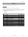
The following table refers to the 50 way D-type plug on the rear of the card
PIN
USAGE
PIN
1
2
3
Analogue input 0 (+ve)
Analogue input 1 (+ve)
Analogue input 2 (+ve)
18
19
20
4
21
7
8
9
10
11
12
13
14
Analogue input 8 (+ve) or
analogue input 0 (-ve)
Analogue input 9 (+ve) or
analogue input 1 (-ve)
Analogue input 10 (+ve) or
analogue input 2 (-ve)
Analogue Output 1 (sig)
Analogue Ground
Digital Ground
PIO port A, b7 (PA7)
PIO port A, b6 (PA6)
PIO port A, b5 (PA5)
PIO port A, b4 (PA4)
PIO port A, b3 (PA3)
15
16
17
PIO port A, b2 (PA2)
PIO port A, b1 (PA1)
PIO port A, b0 (PA0)
5
6
USAGE
PIN
USAGE
34
35
36
Analogue input 5(+ve)
Analogue input 6(+ve)
Analogue input 7 (+ve)
37
22
Analogue input 3 (+ve)
Analogue input 4 (+ve)
Analogue input 11 (+ve)
or analogue input 3 (-ve)
Analogue input 12 (+ve)
or analogue input 4 (-ve)
Analogue Ground
23
Analogue Output 2 (sig)
39
24
25
26
27
28
29
30
31
Analogue Output 0 (sig)
Analogue Ground
PIO port B, b7 (PB7)
PIO port B, b6 (PB6)
PIO port B, b5 (PB5)
PIO port B, b4 (PB4)
PIO port B, b3 (PB3)
PIO port B, b2 (PB2)
40
41
42
43
44
45
46
47
32
33
PIO port B, b1 (PB1)
PIO port B, b0 (PB0)
48
49
50
Analogue input 13 (+ve) or
analogue input 5 (-ve)
Analogue input 14 (+ve) or
analogue input 6 (-ve)
Analogue input 15 (+ve) or
analogue input 7 (-ve)
Analogue Output 3 (sig)
Analogue Ground
Digital Ground
PIO port C, b7 (PC7)
PIO port C, b6 (PC6)
PIO port C, b5 (PC5)
PIO port C, b4 (PC4)
PIO port C, b3 (PC3) and/or
Interrupt Source or Counter
input
PIO port C, b2 (PC2)
PIO port C, b1 (PC1)
PIO port C, b0 (PC0) and/or
Interrupt Source or Counter
input
38
The following diagram shows how the pins on the male D-type connector are numbered
If you are having difficulty in obtaining suitable cables to attach to the PCI-ADC, or you wish to
make your own, the Farnell part numbers for suitable connectors are 1084683 and 4155312.
Chapter 3
Blue Chip Technology
Page 11 of 33
PCI-ADC
Connection Details
Suitable Interface Signal Types
Analogue Inputs
The analogue inputs have a full scale input voltage, dependant on input gain, of between ± 5 mV
and ± 5 volts.
The inputs may be configured as differential (eight inputs) in which case the input voltage must be
applied between the +ve and -ve input connections, or as single ended (sixteen inputs) in which
case the input voltage must be applied between the +ve input and analogue ground. In either case,
the maximum voltage that may be applied between any input connection and analogue ground is
±17 volts. Voltages in excess of these will cause damage.
Analogue Outputs
The four analogue outputs may be individually configured to provide full scale outputs of ± 10
volts or ± 20 mA constant current.
In voltage output mode, the output driver is capable of supplying up to ± 20mA so that full scale
output is available into a minimum load of 500 ohms.
In current output mode, the output driver is capable of supplying up to ± 12 volts, therefore the
maximum load that may be driven to full scale is 600 ohms. The current is provided by the onboard supply.
Voltage or current outputs are referenced to analogue 0 volts, for which there are several pins
available on the I/O connector.
Chapter 3
Blue Chip Technology
Page 12 of 33
PCI-ADC
Connection Details
Digital I/O
The input and output signals for the PCI-ADC parallel ports and counter/timers are strictly digital
TTL levels with voltage limits of zero volts for a logic low and +5 volts for a logic high. Voltages
outside these limits may cause damage to the card. The output current drive capability makes the
card suitable for connection to TTL logic type circuits. The PCI-ADC is compatible with most
types of TTL logic. Because the lines are TTL it is recommended that input signal lines do not
exceed 2 metres in length. Operation at longer lengths may cause drive level problems.
Driving conventional relay coils is not recommended without external protection even if the coil
current required is less than the PCI-ADC can provide. Relay coils are inductive and as such can
generate large flyback voltages when de-energised which will destroy the device outputs.
Counter / Timers
Input signals to two of the counter / timers may be taken from the I/O connector by sacrificing
two bits of one of the I/O ports and configuring them as inputs. The counter timer inputs are then
driven from these I/O lines through 270 Ω (ohm) series protection resistors. The counter / timers
are permanently enabled.
Chapter 3
Blue Chip Technology
Page 13 of 33
PCI-ADC
Programming Details
Chapter 4
This chapter provides brief details of the cards internal registers.
Address Map
The address map for the PCI-ADC occupies a 26-byte block of addresses.
All the following addresses are relative to the addresses contained in PCI Base Address Registers
2, 3 and 4 (BAR2, BAR3 & BAR4) as indicated. These base address registers are located at the
following addresses in the PCI configuration space:Base 2 = 18h
Base 3 = 1Ch
Base 4 = 20h
ADDRESS
(hex)
Base 2 + 0
Base 2 + 1
Base 2 + 2
Base 2 + 3
Base 2 + 4
Base 2 + 5
Base 2 + 6
Base 2 + 7
Base 2 + 8
Base 2 + 9
Base 2 + A
Base 2 + B
Base 2 + C
Base 2 + D
Base 2 + E
Base 2 + F
Base 3 + 0
Base 4 + 0
Base 4 + 2
Base 4 + 4
Base 4 + 6
Chapter 4
FUNCTION
PIO Port A Input/Output Register (Channel 0 to 7)
PIO Port B Input/Output Register (Channel 8 to 15)
PIO Port C Input/Output Register (Channel 16 to 23)
PIO Control Register
Counter/timer 0 Count Register
Counter/timer 1 Count Register
Counter/timer 2 Count Register
Counter/timer Control Register
Counter Control Register
Interrupt Enable Register
Interrupt Status Register
Analogue Output Control Register
Analogue conversion control register
Analogue input select register
Analogue input status register
Not used
Analogue input sample
Analogue output sample, Channel 0
Analogue output sample, Channel 1
Analogue output sample, Channel 2
Analogue output sample, Channel 3
Blue Chip Technology
ACCESS
WIDTH
READ/
WRITE
byte
byte
byte
byte
byte
byte
byte
byte
byte
byte
byte
byte
byte
byte
byte
byte
word
word
word
word
word
R/W
R/W
R/W
W
R/W
R/W
R/W
W
R/W
R/W
R
R/W
R/W
R/W
R
R
R/W
R/W
R/W
R/W
Page 14 of 33
PCI-ADC
Programming Details
Analogue Inputs
Each analogue sample is represented on the PCI data bus as a 16 bit word, the lower 12 bits of
which represent the analogue value, and the upper four bits represent the channel number.
The analogue sample is represented by a twelve bit two’s complement number,
+5 volts (+ve full scale) gives a code of x7FF h
zero volts input produces a code of x000 h and
-5 volts (-ve full scale) gives a code of x800 h
The basic analogue to digital converter has a full scale input of ± 5 volts. The on-board
programmable gain amplifier allows for lesser voltages at the input pins. Note that there is no
indication of an over-voltage input condition. The value returned will simply be full scale. The
user must ensure that the inputs remain within the full scale input range selected.
The upper 4-bits of the input word represents the channel number. In single ended mode this
number is between 0 and 15 and in differential mode it is between 0 and 7.
The format of the analogue input sample is shown below:Analogue Input Sample
Bit no.
b15..b12
b11..b0
(Base 3 + 0) Read only
Function
Converted channel number (0 - 15 for single ended inputs)
(0 - 7 for differential inputs)
Two’s complement analogue input sample
For example, Looking at this in binary we have Bits 13 to 16 represent the analogue input channel
16th _ _ _ _ _ _ _1st bit
0000 0111 1111 1111 +5 volts on analogue input 0 or 07FFh
1000 0111 1111 1111 +5 volts on analogue input 8 or 87FFh
0000 1000 0000 0000 -5 volts on analogue input 0 or 0800h
1000 1000 0000 0000 -5 volts on analogue input 8 or 8800h
Chapter 4
Blue Chip Technology
Page 15 of 33
PCI-ADC
Programming Details
FIFO Memory
The Analogue Input Samples are stored in a 16-bit wide, 1024-word deep First-In, First-Out
(FIFO) memory.
FIFO memory is well suited to transferring data between two asynchronous systems i.e. between
the regular, clocked analogue samples, and irregular, software dependent processor intervention.
If this FIFO memory is not required, it may be ignored, as its actions are transparent to the user.
For example, if a single channel is to be converted, then the conversion is initiated and when
complete, indicated by either the ‘busy’ flag being negated, the ‘FIFO empty’ flag being negated,
or from interrupts, the sample may then be read directly from the analogue input sample port.
If, however, a series of samples are required before any processing begins, or the software
overhead of reading the card is so great that it must be performed infrequently, then the FIFO may
be used to store the samples as they are taken, with processor intervention only being required
when the FIFO is full. The samples may then be read.
Conversion may be initiated under software control, or by a hardware trigger which may be
generated either from counter/ timer 0, 1, or 2, or from an external trigger input.
The ADC busy and FIFO flags are accessible in the Analogue Input Status Register (see below).
Conversion Control
Conversion may be of a single channel, or of a number of channels, scanned sequentially. It may
be initiated under software control or by a hardware trigger from a number of sources. Single
channel conversion is normally initiated under software control. Conversion of a number of
channels would normally be under hardware control, although software control is feasible.
Two registers control the ADC section: the Input Select Register and the Conversion Control
Register. Both have a number of functions. The Input Select Register controls the input channel,
the gain, and the selection of single, differential or calibration inputs. The Conversion Control
Register selects the conversion trigger source, whether a single or multiple channels are to be
converted, and whether conversion is single or continuous.
Interrupts may be generated on the following conditions (see Interrupt Status Register):•
•
•
Chapter 4
ADC not busy (i.e. conversion complete)
FIFO half full
FIFO not empty
Blue Chip Technology
Page 16 of 33
PCI-ADC
Programming Details
The Analogue Conversion Control Register at Base 2 + 0C h is used to specify the type of
conversion to be performed. The functions of the bits within this register are described below:Analogue Conversion Control Register (Base 2 + 0C h) Read/write.
Bit no.
Function
b4..b2
b1
b0
Conversion trigger:-
000 = No trigger
001 = Software trigger
010 = PC0 input port line
011 = PC3 input port line
100 = Counter/timer 0 output (see Note)
101 = Counter/timer 1 output (see Note)
110 = Counter/timer 2 output (see Note)
111 = Not used.
Conversion Trigger mode:- 0 = edge triggered (single conversion)
1 = level triggered (multiple conversions)
Input Channel Selection:0 = Manual selection of single channel
1 = Automatic selection & increment
Note: Triggers from the counter / timer outputs occur on the high-to-low transition of the output.
Most counter / timer modes operate in this manner.
If manual selection of the input channel is set, then a conversion of the channel specified in the
Analogue Input Select Register, will be performed whenever a trigger condition occurs.
The trigger condition may be selected from the list shown in the table. For all trigger modes, it is
necessary to select whether the trigger is edge or level triggered.
If edge trigger is selected, then a new conversion will not occur until the trigger (from whatever
source) has been negated and re-asserted i.e. the conversion is initiated on the low to high
transition of the trigger source. This ensures that only one conversion takes place.
If level trigger is selected, then conversions will be performed for as long as the trigger source is
present.
If a software trigger is selected (by setting bits 4..2, to 001) in combination with edge triggering,
then the selected channel will be converted immediately. Bits 4 to 2 will then be automatically
cleared to 000 ready for the next conversion. It is possible to determine when the conversion has
been completed either by reading the Analogue Input Status Register (as with all other trigger
modes) or by reading bit 2 of the Conversion Control Register to see when it is cleared to zero.
If software trigger is selected in combination with level triggering, then a new conversion will be
initiated immediately the previous conversion has been completed, and continues until the
software trigger is negated. There are limitations to the use of level triggering (see later).
Chapter 4
Blue Chip Technology
Page 17 of 33
PCI-ADC
Programming Details
Input Mode Selection and Calibration
The Analogue Input Select Register is used to select either the single channel for conversion, or
the range of channels to be converted.
In the automatic mode, the first conversion will be of the channel selected in the Analogue Input
Select Register, as the highest numbered channel. The first conversion may contain spurious
information and it is recommended that it be discarded. The next conversion will be of channel
zero, and every subsequent conversion will be to the next numeric channel up to and including the
channel number specified in the Analogue Input Select Register. The channel number will then
return to zero for the next conversion and the channel scan will be repeated.
The input mode of the analogue samples may be selected to be single ended (up to 16 channels) or
differential (up to 8 channels). If the number of channels to be scanned in differential mode is
greater than eight, then only eight channels (0-7) will be scanned.
A zero volt or a positive voltage close to full scale may also be selected as inputs to provide a
calibration facility.
The input gain for the chosen channel when selecting manually, or for all channels, when
selecting automatically, may be set to 1, 10, 100 or 1000. At higher gains or when extreme
accuracy is required, it is recommended that auto-calibration be performed (see “AutoCalibration” below) to remove inherent offset or gain errors.
Analogue Input Select Register
Bit no.
b7..b4
b3..b2
b1..b0
(Base 2 + 0D h) Read/write
Function
Channel number (Manual selection)
-ORNumber of channels to be scanned 0 - 15 for single ended inputs
(Automatic select & increment)
0 - 7 for differential inputs
Input gain:00 = 1
01 = 10
10 = 100
11 = 1000
Input mode:00 = Single ended inputs
01 = Differential inputs
10 = Calibration zero volts input
11 = Calibration + 80% full scale input
The accuracy that may be achieved with and without auto-calibration, is listed in the
Specifications section.
Chapter 4
Blue Chip Technology
Page 18 of 33
PCI-ADC
Programming Details
Auto-Calibration
If auto-calibration is required, select the gain that will be used and zero input, and then take ten
samples over a period of between 1 millisecond and 1 second. Take the mean of these samples.
Then select a gain of 1 and “PCI” -positive calibration input (this is actually 80% of full scale to
avoid limiting) and take ten more samples over a similar period. Take the mean of these samples.
The calibrated outputs may then be calculated with the following equation:Calibrated sample = [raw sample - mean zero sample] * [1- ( {PCI/2047}- 0.8) ]
The reason for taking ten samples and using the mean of these in the calculation is to minimise
the effects of noise on the measurements, as any noise on a single calibration sample will
otherwise effect all future measurements.
The major gain errors are associated with the A-D converter and not with the input gain stages.
The major offset errors are associated with the input gain stages and not with the A-D converter.
This is why the zero samples (used to determine offsets) are measured at the required gain, whilst
the full scale samples (used to determine gain errors) are measured at minimum gain.
Note that when reading either the calibration zero or positive input, the channel number stamped
on the returned value is not meaningful.
Analogue Input Status
To determine the operating status of the analogue input section, the analogue input status register
is available at Base + 0E h. This register allows access to the status of the A-D converter ‘busy’
flag, the ‘FIFO full’ flag, the ‘FIFO half full’ flag, and the ‘FIFO empty’ flag.
Analogue Input Status Register (Base 2 + 0E h) Read only
Bit no.
Function
b7..b3
b3
b2
b1
b0
Not used (set to zero)
FIFO ‘Full’ Flag:-
0 = Not Full.
1 = Full.
FIFO ‘Half Full’ Flag:0 = Not Half Full.
1 = Half Full.
FIFO ‘Empty’ Flag:0 = Not Empty.
1 = Empty.
A-D Converter ‘Busy’ flag:- 0 = Conversion complete
1 = Conversion in progress
Once the FIFO is full, conversions may continue to take place but will be discarded. The FIFO
prevents the storage of further values whilst the ‘Full’ flag is asserted. Reading one value from
the FIFO will negate the Full flag and allow one more conversion to be stored, which will not be
sequential with the previously stored values. To avoid this situation occurring, it is recommended
that the ‘Half Full’ flag be used to initiate FIFO reads.
Reading an empty FIFO will return a value 0FFFFh.
Chapter 4
Blue Chip Technology
Page 19 of 33
PCI-ADC
Programming Details
To Start A Conversion
If necessary, clear the Analogue Conversion Control Register (ACCR) by writing 00 to the
address Base 2 + 0Ch.
Set the Analogue Input Select Register (at address Base 2 + 0Dh), to the required channel, gain
and input mode.
Allow the settling time (if necessary).
Write to the ACCR to select the trigger source, edge or level trigger, and single or multiple
channels for conversion.
Poll the Analogue Input Status Register (at Base 2 + 0Eh) for FIFO Not Empty, or Conversion
Complete. Alternatively, interrupts may be used (see section “Interrupt Selection”).
Limitations to Use
Level triggering of the conversion is provided to allow the rapid monitoring of a single input
channel. It gives a high sample rate (the “burst rate”) for a limited period, usually until the FIFO
is full. Conversions will continue when the FIFO is full, but the results will not be stored until the
FIFO is at least partially empty. Subsequent conversions will then be stored until the FIFO is
again full.
Level triggering provides conversions as fast as the ADC can service them with no allowance
made for the switching and settling times of the multiplexers or the programmable gain amplifier.
Attempting to convert multiple channels using level control will result in erroneous results
because the differing inputs will not have sufficient time to settle.
During any conversion, allowance must be made for the switching and settling times of the
multiplexers and the programmable gain amplifier. The times vary with amplifier gain. The table
below gives typical settling times for the available gain settings.
Analogue Input Settling Times
Gain
1
10
100
1000
Typical Settling Time to 0.1%
9 µs
11 µs
80 µs
600 µs
In most edge triggered conditions particularly those from external events, the delay will be
inherent in waiting for the trigger condition to occur. Allowance will be required when using
software triggering. This is achieved by delaying writing to the Analogue Conversion Control
Register after writing to the Analogue Input Selection Register.
Chapter 4
Blue Chip Technology
Page 20 of 33
PCI-ADC
Programming Details
Analogue Outputs
Each analogue output is written as one 12 bit word to one of four word addresses, each address
representing the analogue output channel to be updated (see Address Map section).
Analogue Output Channel 0
(Base 4 + 0) Read/write
Bit no.
Function
b15..b12 Not used
b11..b0 Output sample (offset binary)
Analogue Output Channel 1
(Base 4 + 2) Read/write
Bit no.
Function
b15..b12 Not used
b11..b0 Output sample (offset binary)
Analogue Output Channel 2
(Base 4 + 4) Read/write
Bit no.
Function
b15..b12 Not used
b11..b0 Output sample (offset binary)
Analogue Output Channel 3
(Base 4 + 6) Read/write
Bit no.
Function
b15..b12 Not used
b11..b0 Output sample (offset binary)
Whenever a new word is written, the relevant analogue output will be updated immediately.
The values written to the four analogue output sample addresses may be read back unaltered from
the same addresses.
Each output channel may be configured to provide either a constant voltage source (up to ± 10
volts) or a constant current source (up to ± 20 mA) by writing to four bits in the Analogue Output
Control Register at Base + 0B h. Note the minimum and maximum loads stated in the section
“Suitable Interface Signal Types”.
Analogue Output Control Register
(Base 2 + 0B h) Read/write
Bit no.
Function
b7..b4 Not used
b3
b2
b1
b0
Chapter 4
Channel 3 output format :- 0 = Constant voltage
1 = Constant current
Channel 2 output format :- 0 = Constant voltage
1 = Constant current
Channel 1 output format :- 0 = Constant voltage
1 = Constant current
Channel 0 output format :- 0 = Constant voltage
1 = Constant current
Blue Chip Technology
Page 21 of 33
PCI-ADC
Programming Details
The output voltage is an offset binary version of the input data, i.e. the output voltage will be
-10 volts for an input code of 0000h, or in binary 0000 0000 0000 0000
zero volts for an input code of 07FFh, or in binary 0000 0111 1111 1111
+10 volts for an input code of 0FFFh. Or in binary 0000 1111 1111 1111
For example if we want to set -5V or +5V
for –5V output write 03FF h ( 0000 0011 1111 1111 )
for 5V output write 0BFF h ( 0000 1011 1111 1111 )
When set to current output mode the corresponding outputs are
-20 mA (0000h),
0 mA (07FFh),
+20 mA (0FFFh).
On power up or card reset, the output voltages will automatically reset to zero volts (0 mA).
Chapter 4
Blue Chip Technology
Page 22 of 33
PCI-ADC
Programming Details
Digital I/O
An Intel i8255 PIO device and an Intel i8254 Counter/timer provide the board’s digital
input/output facilities.
The i8255 PIO and i8254 Counter/timer ICs are complex devices. For full details on how to
program these devices, refer to the manufacturer’s data sheets. Presented here is a brief summary
of the main features of each.
i8255 PIO
The PIO chip can operate in one of three modes.
The first (Mode 0) provides for simple inputs and outputs for three, 8-bit ports. Data is written to
or read from a specified port (A, B, or C) without the use of handshaking. The following table
gives a summary of the most commonly used control words which must be written to the control
port to configure the i8255 I/O ports in Mode 0.
CONTROL
WORD (hex)
80
81
82
83
88
89
8A
8B
90
91
92
93
98
99
9A
9B
CONTROL
WORD
(decimal)
128
129
130
131
136
137
138
139
144
145
146
147
152
153
154
155
SET ALL
of PORT A
as
Output
Output
Output
Output
Output
Output
Output
Output
Input
Input
Input
Input
Input
Input
Input
Input
SET ALL
of PORT
B as
Output
Output
Input
Input
Output
Output
Input
Input
Output
Output
Input
Input
Output
Output
Input
Input
SET HIGH
4 BITS of C
as
Output
Output
Output
Output
Input
Input
Input
Input
Output
Output
Output
Output
Input
Input
Input
Input
SET LOW
4 BITS of
C as
Output
Input
Output
Input
Output
Input
Output
Input
Output
Input
Output
Input
Output
Input
Output
Input
A typical sequence of events to use mode 0 would be :
●
Decide on the mix of input/outputs required and write the appropriate code to the Control
Register (see Address map).
●
Read from the selected input port or write to the selected output port.
Chapter 4
Blue Chip Technology
Page 23 of 33
PCI-ADC
Programming Details
Mode 1 enables the transfer of data to or from a specified 8 bit port (A or B) in conjunction with
strobes or handshaking signals on port C. These handshaking signals may be used to drive
interrupt channels if required.
In Mode 2, data is transferred via one bi-directional 8 bit port (A) with handshaking (port C).
These handshaking signals may be used to drive interrupt channels if required. In this mode port
B is not available.
Refer to the i8255 data sheet for full details of the settings and use of Modes 1 and 2.
i8254 Counter / Timer
The counter/timer circuit contains three independent 16-bit counters which may be operated in a
variety of modes. There are five basic modes of operation with each mode providing a different
output signal. Presented here is a brief summary of some of the modes possible by programming
the counter / timer’s internal registers. Refer to the i8254 data sheet for full details of the settings
and use of the counter / timer.
All three counter/timers may be operated independently, with separate clocks. The clock inputs of
two counter/timers may also be made accessible on the back panel connector. See the Counter
Control Register table for the available clock inputs.
Counter 0, Counter 1 and Counter 2 may also be connected in series. Counter 0 output linked to
Counter 1 clock input and/or Counter 1 output linked to Counter 2 clock input, to allow the
generation of very long delay periods.
The outputs from any counter/timer may be configured to generate an interrupt.
Chapter 4
Blue Chip Technology
Page 24 of 33
PCI-ADC
Programming Details
Counter / Timer Modes
The following modes of operation exist by programming the control register within the i8254.
Mode 0
When programmed, the output pin will go LOW. When the counter decrements from the value
loaded into the count registers to zero, the output pin will go HIGH. It will remain high until the
count is re-programmed into the count registers.
Mode 1
When the count registers are programmed the output pin will be HIGH. When a LOW going
signal is applied to the gate input, the count starts and the output will fall LOW, returning HIGH
at the end of the count. The gate lines are permanently enabled on the PCI-ADC.
Mode 2
This mode operates as a frequency divider. When programmed the output pin is HIGH. When
the count decrements to a value of 1 the output pin will go LOW for ONE clock cycle only and
then return HIGH. This cycle repeats continuously without the need to re-program the count
value.
Mode 3
When programmed the output pin will toggle each time the count register decrements to its base
level from the value programmed into it. If the count value loaded is an odd number then the
counter will reach zero before the output pin toggles. This mode therefore acts as a frequency
divider with an approximate 1:1 mark-space ratio.
Mode 4
This mode is similar to mode 2 but the output pin pulses when the count reaches zero instead of 1.
Mode 5
This mode is similar to mode 4 except that the count sequence is triggered by the gate line. The
gate lines are permanently enabled on the PCI-ADC.
Note that Counter / Timer interrupts are generated on the falling edge of the timer outputs. This
may limit the modes in which the timers can be operated as interrupt sources.
Chapter 4
Blue Chip Technology
Page 25 of 33
PCI-ADC
Programming Details
Counter Control
The input lines of the Counter / Timer may be accessed on the rear panel connector by sacrificing
some of the digital I/O lines.
The Counter / Timers are permanently enabled. Counter / Timer 0 is permanently clocked by the
on board 4 MHz oscillator. Counter / Timers 1 and 2 may be clocked from several sources as
shown in the table.
The clock inputs of the i8254 Counter / Timer are selected using the Counter Control Register at
Base 2 + 8, as shown below:-
Bit no.
Counter Control Register (Base 2 + 8) Read/write
Function
b7..b4
b3..b2
Not used
Counter / Timer 2 clock source:-
b1..b0
Counter / Timer 1 clock source:-
00 = 4 MHz on board clock
01 = PC0 port line
10 = Counter 1 output
11 = PC3 port line
00 = 4 MHz on board clock
01 = PC0 port line
10 = Counter 0 output
11 = PC3 port line
To use either port line PC0 or PC3 as an input to the Counter / Timer the i8255 PIO port line must
be configured as an input to avoid contention.
Chapter 4
Blue Chip Technology
Page 26 of 33
PCI-ADC
Programming Details
Interrupt Selection
The use of interrupts is not essential but greatly enhances the functionality of the card. A total of
seven sources of interrupt are available from the PIO device, the counter/timers and the Analogue
input stage. These interrupts are summarised below:• INT0 (PC0) is available when the PIO is operating in mode 1. It provides a Read Request
interrupt for input operations or a Write Request interrupt for output operations on PIO
port A (PA[0:7]).
• INT1 (PC3) is available when the PIO is operating in mode 1. It provides a Read Request
interrupt for input operations or a Write Request interrupt for output operations on PIO
port B (PB[0:7]).
• INT2 is the output from Counter/timer 0, and may be used to generate interrupts on timed
events.
• INT3 is the output from Counter/timer 1, and may be used to generate interrupts on timed
events.
• INT4 is the output from Counter/timer 2, and may be used to generate interrupts on timed
events.
• INT5 is created from the A-D converter ‘Busy’ flag and may be used to indicate when a
Analogue input conversion has been completed. (Interrupt on ‘Busy’ being negated).
• INT6 is created from the FIFO memory ‘Empty’ flag and may be used to indicate when
the FIFO memory is no longer empty i.e. a sample has been taken.
• INT7 is created from the FIFO memory ‘Half Full’ flag and may be used to indicate when
the FIFO memory is half full. This is provided for the cases where the interrupt service
routine cannot be guaranteed to read the FIFO before the next sample is stored.
Note: Counter / Timer interrupts are generated on the falling edge of the timer outputs. This
may limit the modes in which the timers can be operated as interrupt sources.
Chapter 4
Blue Chip Technology
Page 27 of 33
PCI-ADC
Programming Details
To enable an interrupt or a combination of interrupts to be generated, an enable word must be
written to the Interrupt Enable Register at Base 2 + 9 h, as shown below:Interrupt Enable Register (Base 2 + 9 h) Read/write
Bit no.
b7
b6
b5
b4
b3
b2
b1
b0
Function
INT7 control - FIFO Half Full
INT6 control - FIFO Not Empty
INT5 control - ADC Not Busy
INT4 control - Counter/timer 2 output
INT3 control - Counter/timer 1 output
INT2 control - Counter/timer 0 output
INT1 control - PC3 interrupt control
INT0 control - PC0 interrupt control
1 = Enable, 0 = Disable
1 = Enable, 0 = Disable
1 = Enable, 0 = Disable
1 = Enable, 0 = Disable
1 = Enable, 0 = Disable
1 = Enable, 0 = Disable
1 = Enable, 0 = Disable
1 = Enable, 0 = Disable
When an interrupt is recognised by the processor, the source or sources of interrupt may be
determined by reading the Interrupt status register at Base 2 + 0Ah, as shown below:Interrupt Status Register
Bit no.
b7
b6
b5
b4
b3
b2
b1
b0
(Base 2 + 0A h) Read only
Function
INT7 status - FIFO Half Full
INT6 status - FIFO Not Empty
INT5 status - ADC Not Busy
INT4 status - Counter/timer 2 output
INT3 status - Counter/timer 1 output
INT2 status - Counter/timer 0 output
INT1 status - PC3 interrupt status
INT0 status - PC0 interrupt status
Having serviced an interrupt, the source should be cleared by momentarily clearing the relevant
bit in the interrupt enable register.
Chapter 4
Blue Chip Technology
Page 28 of 33
PCI-ADC
Electromagnetic Compatibility
Chapter 5
Electromagnetic Compatibility (EMC)
This product meets the requirements of the European EMC Directive (89/336/EEC) and is eligible to bear the CE
mark.
It has been assessed operating in our standard industrial PC. However, because the board can be installed in a
variety of computers, certain conditions have to be applied to ensure that the compatibility is maintained. It
meets the requirements of EN55022:1995 for a Class A product subject to those conditions.
• The board must be installed in a computer system which provides screening suitable for an industrial
environment.
• Any recommendations made by the computer system manufacturer/supplier must be complied with
regarding earthing and the installation of boards.
• The board must be installed with the backplate securely screwed to the chassis of the computer to ensure
good metal-to-metal (i.e. earth) contact.
• Most EMC problems are caused by the external cabling to boards. It is imperative that any external cabling
to the board is totally screened, and that the screen of the cable connects to the metal end bracket of the
board and hence to earth. It is recommended that round screened cables with a braided wire screen are used
in preference to those with a foil screen and drain wire. Use metal connector shells which connect around
the full circumference of the screen; they are far superior to those which earth the screen by a simple “pigtail”. Standard ribbon cable will not be adequate unless it is contained wholly within the cabinetry housing
the industrial PC.
• Ensure that the screen of the external cable is bonded to a good RF earth at the remote end of the cable.
• Cables which connect externally to boards at TTL levels should not exceed two metres in length.
Failure to observe these recommendations may invalidate the EMC compliance.
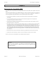
Warning
This is a Class A Product. In a domestic environment this product may
cause radio-interference in which case the user may be required to take
adequate measures.
Chapter 5
Blue Chip Technology
Page 29 of 33
PCI-ADC
Electromagnetic Compatibility
EMC Specification
A suitably compliant industrial PC fitted with this card meets the requirements of the European
Union Electromagnetic Compatibility Directive 89/336/EEC and its amending Directives, and
specifically the following standards:
Chapter 5
Emissions
EN 55022:1998 Class A
Immunity
EN 55024:1998
Blue Chip Technology
Page 30 of 33
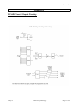
PCI-ADC
Input / Output
Chapter 6
PCI-ADC Input / Output Circuitry
Chapter 6
Blue Chip Technology
Page 31 of 33
PCI-ADC
Chapter 6
Input / Output
Blue Chip Technology
Page 32 of 33
Product Form Factor
History
Amendment History
Issue Level
1.0
1.1
Issue Date
12/01/2007
07/02/2007
Author
Tmck
Tmck
21/03/2007
TMCK
1.2
Amendment Details
First Release
Added MTBF figure and some grammar changes, corrected EMC
details
Corrected reversed diagram and updated Autocal equation
Contact Details
Blue Chip Technology Ltd.
Chowley Oak
Tattenhall
Chester
CH3 9EX
U.K.
Telephone: +44 (0)1829 772000
Facsimile: +44 (0)1829 772001
www.bluechiptechnology.co.uk
Plasma PC Sales
[email protected]
Single Board Computer Sales
[email protected]
Rack mount PC Sales
[email protected]
Data and IO Sales
[email protected]
Technical Support
[email protected]