1
APPLICATION NOTE
SH7266/SH7267 Groups
E10A-USB Flash Memory Download Function
R01AN1151EJ0100
Rev.1.00
Jun.18, 2012
(Download to the Serial Flash Memory)
Abstract
E10A-USB emulator has the function to download a load module to the flash memory. This function requires a
download program to access the flash memory (hereinafter called the “FMTOOL”).
This document describes how to download a load module to the serial flash memory applying the FMTOOL.
Target Device
SH7266/SH7267 Groups (hereinafter called the “SH7267”)
When using this application note with other Renesas MCUs, careful evaluation is recommended after making
modifications to comply with the alternate MCU.
R01AN1151EJ0100 Rev.1.00
Jun.18, 2012
Page 1 of 29
SH7266/SH7267 Groups
Example of E10A-USB Flash Memory Download Function
(Download to the Serial Flash Memory)
Contents
1.
Specifications .................................................................................................................................... 3
2.
Operation Confirmation Conditions ................................................................................................... 4
3.
Reference Application Note(s) .......................................................................................................... 4
4.
Hardware........................................................................................................................................... 5
4.1 Hardware Configuration ............................................................................................................... 5
4.2 Reference Circuit ......................................................................................................................... 6
5.
Software ............................................................................................................................................ 7
5.1 Operation Overview ..................................................................................................................... 7
5.1.1 Batch File.............................................................................................................................. 7
5.1.2 Erase Module........................................................................................................................ 7
5.1.3 Write Module......................................................................................................................... 8
5.2 File Composition .......................................................................................................................... 9
5.3 Constants ................................................................................................................................... 10
5.4 Structure/Union List ................................................................................................................... 10
5.5 Variables .................................................................................................................................... 11
5.6 Functions.................................................................................................................................... 11
5.7 Function Specifications .............................................................................................................. 12
5.8 Flowchart.................................................................................................................................... 16
5.8.1 Erase Module...................................................................................................................... 16
5.8.2 Write Module....................................................................................................................... 16
5.8.3 Initialization of FMTOOL ..................................................................................................... 17
5.9 Basic Precautions ...................................................................................................................... 19
5.9.1 Adding Dummy Data to the Load Module........................................................................... 19
5.9.2 Forbidding Sharing Sectors between the Load Modules.................................................... 20
5.9.3 Forbiding Sharing Sectors within the Address Conversion Table ...................................... 20
6.
Application Example........................................................................................................................ 22
6.1 Procedure of User Program Download...................................................................................... 22
6.1.1 Prepare for the Download Environment ............................................................................. 22
6.1.2 Registering a Batch File...................................................................................................... 23
6.1.4 Adding a Download Module................................................................................................ 24
6.1.5 Downloading a User Program ............................................................................................ 25
6.2 Application to Serial Flash Boot ................................................................................................. 26
6.2.1 Changes in replacing the Downloader to the FMTOOL ..................................................... 26
6.2.2 Storing and Reading Constant Data................................................................................... 27
6.3 Customizing FMTOOL ............................................................................................................... 28
6.3.1 Device Specification Capable for Sample Code................................................................. 28
7.
Sample Code................................................................................................................................... 29
8.
Reference Documents..................................................................................................................... 29
R01AN1151EJ0100 Rev.1.00
Jun.18, 2012
Page 2 of 29
SH7266/SH7267 Groups
Example of E10A-USB Flash Memory Download Function
(Download to the Serial Flash Memory)
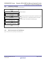
1.
Specifications
Download the load module to the serial flash memory using the FMTOOL that supports the serial flash memory. The
FMTOOL uses the Renesas serial peripheral interface (RSPI) and allows the serial flash memory accessed.
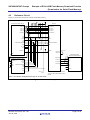
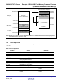
Table 1.1 lists the peripheral functions and the applications. Figure 1.1 shows the procedure of download using the
FMTOOL.
Table 1.1 Peripheral Functions and Applications
Peripheral Function
Renesas Serial Peripheral Interface (RSPI) channel 0
H-UDI
Integrated
development
Execute flash memory environment
download function
Application
Download to the serial flash memory
Connects the E10A-USB emulator
SH7267
E10A-USB
emulator
Renesas serila peripheral
interface
Serial flash
memory
FMTOOL
1. Start butch file
Reset CPU
2. Execute erase module
3. Execute write module
(Repeat by 4 bytes)
Initialize serial flash memroy
Initialize Renesas serial
peripheral interface
Buffering for one page
Write by the page (page: 256 bytes)
Erase by the sector (sector: 64K bytes)
Figure 1.1 Procedure of Download Using FMTOOL
R01AN1151EJ0100 Rev.1.00
Jun.18, 2012
Page 3 of 29
SH7266/SH7267 Groups
Example of E10A-USB Flash Memory Download Function
(Download to the Serial Flash Memory)
2.
Operation Confirmation Conditions
The sample code accompanying this application note has been run and confirmed under the conditions below.
Table 2.1 Operation Confirmation Conditions
Item
MCU used
Device used
Operating frequency
Operating voltage
Integrated development
environment
C compiler
Board used
3.
Contents
SH7267
Serial flash memory
manufacturer: Silicon Storage Technology
model: SST25VF016B
CPU clock (Iφ): 144MHz
Bus clock (Bφ): 72MHz
Peripheral clock (Pφ): 36MHz
Source power (I/O): 3.3V
Source power (internal): 1.25V
Renesas Electronics
High-performance Embedded Workshop Ver.4.07.00
Renesas Electronics
SuperH RISC engine FamilyC/C++ Compiler Package Ver.9.03
Release02
Complier option
-cpu=sh2afpu -fpu=single -include="$(WORKSPDIR)\inc" object="$(CONFIGDIR)\$(FILELEAF).obj" -debug -gbr=auto chgincpath -errorpath -global_volatile=0 -opt_range=all infinite_loop=0 -del_vacant_loop=0 -struct_alloc=1 -nologo
R0K572670C000BR
Reference Application Note(s)
For additional information associated with this document, refer to the following application note(s).
• SH7266/SH7267 Groups Boot From the Serial Flash Memory
(document No.: R01AN0214EJ)
• SH7262/SH7264 Groups Renesas Serial Peripheral Interface Serial Flash Memory Connection Sample Program
(document No.: REJ06B1001)
• Flash Memory Download Program for the E10A-USB Emulator Application Note (document No.:R01AN0957EJ)
R01AN1151EJ0100 Rev.1.00
Jun.18, 2012
Page 4 of 29
SH7266/SH7267 Groups
Example of E10A-USB Flash Memory Download Function
(Download to the Serial Flash Memory)
4.
Hardware
4.1
Hardware Configuration
Table 4.1 lists the used pins and their functions.
Table 4.1 Used Pins and Their Functions
Pin name
Input/Output
Function
RSPCK0
Output
Clock output to the serial flash memory
SSL00
Output
Output device selection signal to the serial flash memory
MOSI0
Output
Data output to the serial flash memory
MISO0
Input
Data input from the serial flash memory
MD_BOOT0
Input
Selection of boot mode (bit 0)
MD_BOOT1
Input
Selection of boot mode (bit 1)
AUDCK
Output
Clock output to the E10A-USB emulator (38-pin)
AUDATA0
Output
Address output to the E10A-USB emulator (38-pin) (bit 0)
AUDATA1
Output
Address output to the E10A-USB emulator (38-pin) (bit 1)
AUDATA2
Output
Address output to the E10A-USB emulator (38-pin) (bit 2)
AUDATA3
Output
Address output to the E10A-USB emulator (38-pin) (bit 3)
AUDSYNC#
Output
Synchronous signal output to the E10A-USB emulator (38-pin)
TCK
Input
Clock input from the E10A-USB emulator
TMS
Input
Mode selection from the E10A-USB emulator
TRST#
Input
Reset input from the E10A-USB emulator
TDI
Input
Data input from the E10A-USB emulator
TDO
Output
Data output to the E10A-USB emulator
ASEBRKAK#/ASEBRK#
Input/Output
Break request and response
RES#
Input
System reset signal
ASEMD#
Input
Selection of ASE mode
Note:“#” indicates a negative-true logic or an active low.
R01AN1151EJ0100 Rev.1.00
Jun.18, 2012
Page 5 of 29
SH7266/SH7267 Groups
Example of E10A-USB Flash Memory Download Function
(Download to the Serial Flash Memory)
4.2
Reference Circuit
Figure 4.1 shows the connection with the serial flash memory.
3.3V
3.3V
3.3V
H-UD port connector (38-pin)
1
SH7267
AUDCK
PF0/AUDCK
AUDATA0
PF2/AUDATA0
AUDATA1
PF3/AUDATA1
AUDATA2
PF4/AUDATA2
AUDATA3
PF5/AUDATA3
AUDSYNC#
PF1/AUDSYNC#
TCK
TCK
TMS
TMS
TRST#
TRST#
TDI
TDI
TDO
TDO
ASEBRKAK#/ASEBRK#
ASEBRKAK#/ASEBRK#
RES#
RES#
VCC_TR
VCC
(ASEMD#)*
5
3.3V
3
ASEMD#
Boot mode 1
MD_BOOT1
MD_BOOT0
GND
3.3V
3.3V
Serial flash memory
SST25VF016B (2M bytes)
3.3V
PF9/RSPCK0
H-UDI port connector (14-pin)
SCK
3.3V
4
(ASEMD#)*
TCK
TRST#
2
12
14
GND
TDO
GND
ASEBRKAK#/ASEBRK#
GND
TMS
TDI
RES#
VCC
1
PF10/SSL00
CE#
3
3.3V
PF11/MOSI0
5
7
SI
PF12/MISO0
SO
9
11
3.3V
WP#
3.3V
HOLD#
13
8
RES#
*: For more details on the connection,
refer to the E10A-USB Emulator User’s
Manual.
Note: l “#” indicates a negative-true logic or an active low.
Figure 4.1 Connection Example
R01AN1151EJ0100 Rev.1.00
Jun.18, 2012
Page 6 of 29
SH7266/SH7267 Groups
Example of E10A-USB Flash Memory Download Function
(Download to the Serial Flash Memory)
5.
Software
5.1
Operation Overview
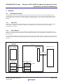
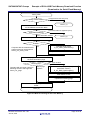
The FMTOOL consists of two programs; the erase module and the write module. The E10A-USB emulator writes
program data and constant data into the flash memory using these programs. For details on the erase module and the
write module, refer to the section “6.22 Downloading to the Flash Memory Area” in the E10A-USB Emulator User’s
Manual.
5.1.1
Batch File
Execute a reset command to initialize the SH7267 using the batch file which has been started before download of the
load module. For details on the batch file and the reset command, refer to the manual listed in the integrated
development environment.
5.1.2
Erase Module
Figure 5.1 shows the outline of the erase module in the FMTOOL. When downloading of the load module starts, the
FMTOOL is transmitted to the high-speed on-chip RAM on the SH7267. The erase module is executed only once after
the transmission.
The erase module usually has the function for chip erase processing of the flash memory. Unlike this typical processing,
the initialization of the Renesas serial peripheral interface and the cancellation of protect setting in the flash memory are
executed.
.
Integrated
development
environment
SH7267
Renesas serial
peripheral interface
User’s program
Serial flash memory
Cancel protect
FMTOOL
High-speed on-chip
RAM
Erase module
Erase module
Execute
copy
Write module
Write module
Address
conversion table
Address
conversion table
Figure 5.1 Erase Module Outline
R01AN1151EJ0100 Rev.1.00
Jun.18, 2012
Page 7 of 29
SH7266/SH7267 Groups
Example of E10A-USB Flash Memory Download Function
(Download to the Serial Flash Memory)
5.1.3
Write Module
Figure 5.2 shows the outline of the write module in the FMTOOL. The write module is executed repeatedly in the highspeed on-chip RAM when downloading of the load module. The write module receives the program data which are
divided into access size as the argument and writes the data to the serial flash memory after calculating the write
destination address for the program data and buffering such data on a per-page basis. When the write destination
address is in the undeleted sector, writes after erasing the sector.
Integrated
development
environment
SH7267
Renesas serial
peripheral interface
User’s program
Serial flash memory
H'1C00 0000
Long word data
(4 bytes)
Page data
(256 bytes)
Page buffer
H'0001 0000
Page write/
Sector erase
Address
conversion
High-speed on-chip
RAM
FMTOOL
Erase module
Erase module
Execute
copy
Write module
Write moduel
Address
conversion table
Address
conversion table
Figure 5.2 Write Module Outline
The write module executes the address conversion to store the program which arranged in the discontinuous area or the
constant data efficiently to the serial flash memory. Figure 5.3 shows the address conversion of the sample code. The
conversion rule is described in the Address Conversion Table in “5.4 Structure/Union List of this application note”. It
may be changed when needed.
R01AN1151EJ0100 Rev.1.00
Jun.18, 2012
Page 8 of 29
SH7266/SH7267 Groups
Example of E10A-USB Flash Memory Download Function
(Download to the Serial Flash Memory)
CPU address space
H'0000 0000
CS0空間*
CS0
space*
64M bytes
(for
the constant data)
(ROMデータ用)
Serial flash memory address
space (2M bytes)
Sector 0
H'0000 0000
(for Loader program)
H'0000 FFFF
H'0001 0000
Sector 1 to 15
(for Application program)
H'000F FFFF
H'0010 0000
H'03FF FFFF
Sector 16 to 31
(for Constant data)
H'1C00 0000
Large-capacity internal
RAM
960K bytes
(for Application program)
H'1C0E FFFF
64K bytes
H'001F FFFF
Prohibited
H'040F FFFF
H'FFF8 0000 High-speed on-chip RAM
(for Loader program)
H'FFF8 FFFF
Note: All areas in the CS0 are suject to address conversion but the area which exceeds the capacity of the
serial flash memory cannnot be used.
Figure 5.3 Address Conversion of Sample Code
5.2
File Composition
Table 5.1 lists the file composition. The files generated by the integrated development environment should not be listed
in this table.
Table 5.1 File Composition
File Name
fm_entry.src
Outline
Entry module of FMTOOL
fm_main.c
fm_cpg.c
fm_r_sf_rspi.c
fm_io_rspi.c
Main module of FMTOOL
Initialization of CPG
Serial flash memory processing
Control processing of the Renesas
serial peripheral interface
Address conversion table
I/F definition of fm_cpg.c
I/F definition of fm_r_sf_rspi.c
I/F definition of fm_io_rspi.c
I/F definition of fm_map.c
Batch file
fm_map.c
cpg.h
r_sf_rspi.h
io_rspi.h
map.h
sh7267_slash_fmtool.hdc
dummy.c
Dummy data definition of the load
module
R01AN1151EJ0100 Rev.1.00
Jun.18, 2012
Remarks
Entry of erase module and write
module
Called function from the entry
Used for the project on the load
module
Used for the project on the load
module.
Page 9 of 29
SH7266/SH7267 Groups
Example of E10A-USB Flash Memory Download Function
(Download to the Serial Flash Memory)
5.3
Constants
Table 5.2 lists the constants used in the sample code.
Table 5.2 Constants Used in the Sample Code
Constant Name
SF_PAGE_SIZE
PAGE_SIZE
SF_SECTOR_SIZE
SECTOR_SIZE
SF_REQ_PROTECT
SF_REQ_UNPROTECT
SR_Init
DEFAULT_VALUE
Setting Value
256
SF_PAGE_SIZE
(64*1024)
SF_SECTOR_SIZE
0
1
0x000000F0
0xFFFFFFFF
TYPE_BYTE
0x4220
TYPE_WORD
0x5720
TYPE_LONG
0x4C20
FM_END_OF_TABLE
0xFFFFFFFF
5.4
Contents
Page size (256 bytes)
ditto
Sector size (64K bytes)
ditto
Sets protect in the serial flash memory
Cancels the protect in the serial flash memory
Status register initial value
Initial value of management data used by
FMTOOL
R5 parameter of write module
(data access size : byte-size)
R5 parameter of write module
(data access size: word-size)
R5 parameter of write module
(data access size: long-size)
Value which indicates the last element of the
address conversion table
Structure/Union List
Figure 5.4 shows the structure/union used in the sample code.
/* Structure of definition for the address conversion table */
typedef struct
{
uint32_t src_top;
/* starting address (source) */
uint32_t src_end;
/* ending address+1 (source) */
uint32_t dest_top;
/* starting address (destination) */
} addr_tbl_t;
/* Address conversion table */
const addr_tbl_t g_fm_addr_tbl[] =
{
/* src_top, src_end,
dest_top */
{0xFFF80000, 0xFFF90000, 0x00000000},
{0x1C000000, 0x1C0F0000, 0x00010000},
{0x00000000, 0x04000000, 0x00100000},
{FM_END_OF_TABLE, 0, 0}
};
/* high-speed on-chip RAM (Loader program) */
/* large-capacity internal RAM (cache effective space) */
/* CS0 space (constant data) */
Figure 5.4 Structure/Union Used in the Sample Code
R01AN1151EJ0100 Rev.1.00
Jun.18, 2012
Page 10 of 29
SH7266/SH7267 Groups
Example of E10A-USB Flash Memory Download Function
(Download to the Serial Flash Memory)
5.5
Variables
Table 5.3lists the global variables. Table 5.4 lists the static variables
Table 5.3 Global Variables
Type
addr_tbl_t
Variable Name
g_fm_addr_tbl
Contents
Address conversion table
Function Used
fmtool_write
Contents
Management information of
erased sectors
Starting address of buffering
pages
Page buffer
Function Used
fmtool_init,
fmtool_write
fmtool_init,
fmtool_write
fmtool_write
Table 5.4Static Variables
Type
uint32_t
Variable Name
fmtool_pre_erase_sctno
uint32_t
fmtool_cur_page
uint32_t
fmtool_page_buf[PAGE_SIZE /
sizeof(uint32_t)]
5.6
Functions
Table 5.5 lists the functions.
Table 5.5 Functions
Function Name
_ERASE_ENTRY
_WRITE_ENTRY
fmtool_init
fmtool_write
R_SF_RSPI_Init
R_SF_RSPI_CtrlProtect
R_SF_RSPI_EraseChip
R_SF_RSPI_EraseSector
R_SF_RSPI_ByteProgram
R_SF_RSPI_ByteRead
io_set_cpg
io_init_rspi
io_cmd_exe
io_cmd_exe_rdmode
R01AN1151EJ0100 Rev.1.00
Jun.18, 2012
Outline
Entry processing for erase module
Entry processing for write module
Main processing for erase module (initialization)
Main processing for write module (erase/write processing)
Serial flash memory operating function
(initialization of Renesas serial peripheral interface and serial flash
memory)
Serial flash memory operating function (protect control)
Serial flash memory operating function (chip erase processing)
Serial flash memory operating function (sector erase processing)
Serial flash memory operating function (write processing)
Serial flash memory operating function (read processing)
* Not available in the sample code.
Initialization of clock pulse generator (CPG)
Initialization of the Renesas serial peripheral interface (RSPI)
Out put processing for RSPI
Input processing for RSPI
Page 11 of 29
SH7266/SH7267 Groups
Example of E10A-USB Flash Memory Download Function
(Download to the Serial Flash Memory)
5.7
Function Specifications
The following tables list the sample code function specifications.
_ERASE_ENTRY
Outline
Header
Declaration
Description
Argument
Returned value
Remarks
_WRITE_ENTRY
Outline
Header
Declaration
Description
Argument
Returned value
Remarks
fmtool_init
Outline
Header
Declaration
Description
Argument
Returned value
Remarks
Entry processing for the erase module
None
_ERASE_ENTRY:
Allocates this function in the address H'FFF8 2000 in the entry section of the erase
module which is activated by the E10A-USB flash memory download function. This
module executes fmtool_init function after setting the stack pointer.
: Access size
R4 register
(byte: H'4220, word: H'5720, long: H'4C20
None
Described in the assembly language
Entry processing for the write module
None
_WRITE_ENTRY:
Allocates this function in the address H'FFF8 2100 in the entry section of the write
module which is activated by the E10A-USB flash memory download function. This
module executes fmtool_write function after setting the stack pointer.
R4 register
: Address where the write data are allocated
R5 register
: Access size
(byte: H'4220, word: H'5720, long: H'4C20)
R6 register
: Write data
R0 register is 0: normal end
R0 register is 1: error end
Described in the assembly language
Main processing for erase module (initialization)
None
void fmtool_init(void);
Initializes the Renesas serial peripheral interface and the serial flash memory. This
function is executed from the entry point of the FMTOOL (_ERASE_ENTRY).
None
None
R01AN1151EJ0100 Rev.1.00
Jun.18, 2012
Page 12 of 29
SH7266/SH7267 Groups
Example of E10A-USB Flash Memory Download Function
(Download to the Serial Flash Memory)
fmtool_write
Outline
Header
Declaration
Description
Argument
Returned value
Remarks
R_SF_RSPI_Init
Outline
Header
Declaration
Description
Argument
Returned value
Remarks
Main processing for the write module (erase/write processing)
None
int32_t fmtool_write(uint32_t addr, int32_t access_size, uint32_t write_data);
Executes erase and write processing in the serial flash memory. The serial flash
memory is accessed by the sector for erasing and by the page for writing. This
function is executed from the entry point of the FMTOOL (_WRITE_ENTRY).
First argument: addr
: Address where the write data are allocated
Second argument: size
: Access size
(byte: H'4220, word: H'5720, long: H'4C20)
Third argument: write_data
: Write data
0: normal end
negative value: error end
Only long word size is available for the access size.
Serial flash memory operating function
(initialization of Renesas serial peripheral interface and serial flash memory)
“r_sf_rspi.h”
void R_SF_RSPI_Init(void);
Initializes the basic part of the Renesas serial peripheral interface. Cancels protect in
the serial flash memory.
None
None
R_SF_RSPI_CtrlProtect
Serial flash memory operating function (protect control)
Outline
“r_sf_rspi.h”
Header
void R_SF_RSPI_CtrlProtect(en_sf_req_t req);
Declaration
Sets/cancels protect in the serial flash memory.
Description
First argument: req
: protect request
Argument
(SF_REQ_PROTECT: sets protect
SF_REQ_UNPROTECT: cancels protect)
None
Returned value
Remarks
R_SF_RSPI_EraseChip
Serial flash memory operating function (chip erase processing)
Outline
“r_sf_rspi.h”
Header
void R_SF_RSPI_EraseChip(void);
Declaration
Executes a chip erase in the serial flash memory.
Description
None
Argument
None
Returned value
Remarks
R01AN1151EJ0100 Rev.1.00
Jun.18, 2012
Page 13 of 29
SH7266/SH7267 Groups
Example of E10A-USB Flash Memory Download Function
(Download to the Serial Flash Memory)
R_SF_RSPI_EraseSector
Serial flash memory operating function (sector erase processing)
Outline
“r_sf_rspi.h”
Header
void R_SF_RSPI_EraseSector(int32_t sector_no);
Declaration
Executes a sector erase in the serial flash memory.
Description
First argument: sector_no
: sector number to be erased
Argument
None
Returned value
Remarks
R_SF_RSPI_ByteProgram
Serial flash memory operating function (write processing)
Outline
“r_sf_rspi.h”
Header
void R_SF_RSPI_ByteProgram(uint32_t addr, uint8_t * buf, int32_t size);
Declaration
Writes the data specified by the argument to the serial flash memory. Uses the byte
Description
program command (H’02) or the auto-increment addressing, word programming
command (H’AD).
First argument: addr
: write address
Argument
(the address in the serial flash memory)
Second argument: buf
: write data (start address in the buffer)
Third argument: size
: data byte count
None
Returned value
Remarks
R_SF_RSPI_ByteRead
Serial flash memory operating function (read processing)
Outline
“r_sf_rspi.h”
Header
void R_SF_RSPI_ByteRead(uint32_t addr, uint8_t * buf, int32_t size);
Declaration
Reads the area specified by the argument to the serial flash memory and stores in
Description
the buffer. Uses the read command (H’0B).
First argument: addr
: read address
Argument
(the address in the serial flash memory)
Second argument: buf
: start address in the read buffer
Third argument: size
: data byte count
None
Returned value
Not used in the sample code
Remarks
io_set_cpg
Outline
Header
Declaration
Description
Argument
Returned value
Remarks
Initialization of clock pulse generator (CPG)
"cpg.h"
void io_set_cpg(void);
Allows clock supply for the operation frequency and the peripheral module
None
None
R01AN1151EJ0100 Rev.1.00
Jun.18, 2012
Page 14 of 29
SH7266/SH7267 Groups
Example of E10A-USB Flash Memory Download Function
(Download to the Serial Flash Memory)
io_init_rspi
Outline
Header
Declaration
Description
Argument
Returned value
Remarks
io_cmd_exe
Outline
Header
Declaration
Description
Argument
Returned value
Remarks
io_cmd_exe_rdmode
Outline
Header
Declaration
Description
Argument
Returned value
Remarks
Initialization of the Renesas serial peripheral interface (RSPI)
"io_rspi.h"
void io_init_rspi(void);
Initializes the channel 0 in the RSPI.
None
None
Output processing for RSPI
"io_rspi.h"
void io_cmd_exe(uint8_t *ope, int32_t ope_sz, uint8_t *data, int32_t data_sz);
Transmits the operation code and the data which are specified by the argument. Sets
the operation code up to 8 bytes.
First argument: ope
Start address in the opcode
Second argument: ope_sz
Size of the opcode
Third argument: data
Start address of the data
Fourth argument: data_sz
Size of the data
None
Input processing for RSPI
"io_rspi.h"
void io_cmd_exe_rdmode(uint8_t *ope, int32_t ope_sz, uint8_t *rd, int32_t rd_sz);
Receives the data in specified size after transmitting the operation code specified by
the argument. Sets the operation code up to 8 bytes.
First argument: ope
Second argument: ope_sz
Third argument: rd
Fourth argument: rd_sz
None
R01AN1151EJ0100 Rev.1.00
Jun.18, 2012
Page 15 of 29
SH7266/SH7267 Groups
Example of E10A-USB Flash Memory Download Function
(Download to the Serial Flash Memory)
5.8
Flowchart
This section describes the procedure of major functions used in the sample code. Regarding the serial flash memory
operating function and the RSIP control procedure, refer to the “SH7262/SH7264 Groups Renesas Serial Peripheral
Interface Serial Flash Memory Connection Sample Program (doc No. REJ06B1001)”.
5.8.1
Erase Module
Figure 5.5shows the procedure of the erase module.
Described in the assembly language
_ERASE_ENTRY
Set a stack pointer
Swap out the register
Swap out the general register of R0 to R7
Execute the main processing of the
module
fmtool_init()
Swap in the register
return
Figure 5.5 Erase Module
5.8.2
Write Module
Figure 5.6 shows the procedure of the write module.
Described in the assembly language
_WRITE_ENTRY
Set a stack pointer
Swap out the general register R1 to R7 to use the
register R0 for the return value
Swap out the register
Execute the main processing of the
module
fmtool_write()
Swap in the register
return (return value of fmtool_write)
Figure 5.6 Write Module
R01AN1151EJ0100 Rev.1.00
Jun.18, 2012
Page 16 of 29
SH7266/SH7267 Groups
Example of E10A-USB Flash Memory Download Function
(Download to the Serial Flash Memory)
5.8.3
Initialization of FMTOOL
Figure 5.7 shows the procedure of initialization of the FMTOOL.
fmtool_init
Set the status register
Disallow interrupts
Set the clock pulse oscillator
io_set_cpg()
Initialize the variable number to be used in
the FMTOOL
Set the following variables in the high-speed on-chip RAM to the initial
value.
- fmtool_pre_erase_sctno : management information on the erased
sectors
- fmtool_cur_page : start address in the buffering page
Initialize the serial flash memory
R_SF_SPIBSC_Init()
Cancel the serial flash memory protect
R_SF_SPIBSC_CtrlProtect()
return
Figure 5.7 Initialization of FMTOOL
5.8.4
Write Processing for the Flash Memory
Figure 5.8 shows the write processing for the flash memory.
R01AN1151EJ0100 Rev.1.00
Jun.18, 2012
Page 17 of 29
SH7266/SH7267 Groups
Example of E10A-USB Flash Memory Download Function
(Download to the Serial Flash Memory)
fmtool_write
Long word access?
Unsupported access size (error)
Yes
return (-1)
Calculate a write destination address based
on the address conversion table
Convertible address?
Conversion table not registered (error)
Detect destination address
return (-2)
Calculate a sector number of the destination
Erased?
Compare with the erased sector
number stored in the argument
fmtool_pre_erase_sctno
No
Execute sector erase
R_SF_RSPI_EraseSector()
Yes
Update the erased sector information
Calculate the page number and the offset in
the write destination page
Buffering page?
Compare with the page number in
buffering stored in the argument
fmtool_cur_page
With page transition
Without page
transition
Write the buffer data (256 bytes) in the
serial flash memory
R_SF_RSPI_ByteProgram()
Clear buffer to H'FF
Update the buffering page
Store the data in the offset position of the
buffer
return (0)
Figure 5.8 Write Processing for the Flash Memory
R01AN1151EJ0100 Rev.1.00
Jun.18, 2012
Page 18 of 29
SH7266/SH7267 Groups
Example of E10A-USB Flash Memory Download Function
(Download to the Serial Flash Memory)
5.9
Basic Precautions
5.9.1
Adding Dummy Data to the Load Module
The FMTOOL writes data by the page with buffering for the purpose of accelerating the write speed to the serial flash
memory. Writing to the serial flash memory is carried in the timing of specifying the address in the page different from
the page under buffering. Therefore it is possible that the data for the last page may be remained in the buffer and not be
written in the serial flash memory. Assign dummy data in the last page of the load module to avoid leaving the valid
data in the buffer.
H'1C00 0000
H'1C00 0000
Write enable
area
Load module
Load module
Write enable area
H'1C00 1EFF
H'1C00 1F00
Write disabled area
H'1C00 1F4B
H'1C00 1F4B
H'1C00 1F4C
Dummy data
H'1C00 1FFF
H'1C00 2000
H'1C00 204B
Write disabled area
Figure 5.9 Write Disabled Area in Load Module
Figure 5.10 shows an example for adding dummy data to the section. Define the constant data of 256 bytes in the
provided dummy section (CDUMMY_MODULE_END) and allocate it at the end of the ROM area.
dummy.c
Locate at the
end of the ROM
area
#pragma section DUMMY_MODULE_END
const char dummy_area[SF_PAGE_SIZE] = { 0 };
#pragma section
#define SF_PAGE_SIZE 256
Figure 5.10 Example of Adding Dummy Data
R01AN1151EJ0100 Rev.1.00
Jun.18, 2012
Page 19 of 29
SH7266/SH7267 Groups
Example of E10A-USB Flash Memory Download Function
(Download to the Serial Flash Memory)
5.9.2
Forbidding Sharing Sectors between the Load Modules
Figure 5.11 shows the operation under the assumption that two load module share one sector. Downloading several load
modules in the FMTOOL is enabled, although sharing one sector between the load modules is disabled. When
downloading multiple data in one sector, the earlier downloaded data is deleted that may be followed by a false
operation.
The mentioned load module area includes the dummy data area described in the section 5.9.1.
Example: Sharing Sector 0 between load module 1 and load module 2.
1. Before writing in load
moduel2
H'0000 0000
Load module
1
2. Start downloading
Execute erase module
3. Execute write module
(Sector erase)
4. Execute write module
(Program)
Load module
1
Sector 0
Delited
Deleted
Before
writing
Before
Load module
writing
Load module
2
2
H'0000 FFFF
Variable controlling
the deleted sector
0
H'FFFF FFFF
(No deleted sector)
0
0
The internal variable is initialized by the erase module,
and sector erase is executed in the write module.
Figure 5.11 Operation when Sharing a Sector between Load Modules
5.9.3
Forbiding Sharing Sectors within the Address Conversion Table
Figure 5.12 shows the operation under the assumption that one sector is shared within the address conversion table. In
the example, g_fm_addr_tbl[0] and g_fm_addr_tbl[1] in the address conversion table share the sector 0, the data written
in the g_fm_addr_tbl[0] will be deleted when downloading the area subject to the g_fm_addr_tbl[1].
Set the value which does not share a write sector in the address conversion table.
R01AN1151EJ0100 Rev.1.00
Jun.18, 2012
Page 20 of 29
SH7266/SH7267 Groups
Example of E10A-USB Flash Memory Download Function
(Download to the Serial Flash Memory)
Example of address conversion table for the sector shared.
Source: Starting address
(src_top)
Source: Ending address+1
(src_end)
Destination: Starting
address
(dest_top)
Write sector
(64KB sector)
g_fm_addr_tbl[0]
H'1C00 0000
H'1C02 0000
H'0000 8000
Sector 0, Sector 1, Sector 2
g_fm_addr_tbl[1]
H'FFF8 0000
H'FFF8 2000
H'0000 0000
Sector 0
Download by g_fm_addr_tbl[0]
Downlaod by g_fm_addr_tbl[1]
Serial flash memory
address space
CPU address space
H'0000 0000
H'1C00 0000
Serial flash memory
address space
CPU address space
H'0000 0000
H'1C00 0000
Deleted
Subject area for
g_fm_addr_tbl[1]
Sector 0
H'0000 8000
Sector 0
Deleted
Subject area for
g_fm_addr_tbl[0]
Subject area for
g_fm_addr_tbl[0]
H'0001 0000
Downlaod
Subject area for
g_fm_addr_tbl[0]
Subject area for
g_fm_addr_tbl[0]
Sector 1
H'0002 0000
H'FFF8 0000
H'0001 0000
Sector 1
H'0002 0000
Sector 2
Subject area for
g_fm_addr_tbl[1]
Subject area for
H'FFF8 0000 g_fm_addr_tbl[1]
Sector 2
Download
Deleted
Figure 5.12 Operation when Sharing a Sector within the Address Conversion Table.
R01AN1151EJ0100 Rev.1.00
Jun.18, 2012
Page 21 of 29
SH7266/SH7267 Groups
Example of E10A-USB Flash Memory Download Function
(Download to the Serial Flash Memory)
6.
Application Example
6.1
Procedure of User Program Download
This section describes the procedure of downloading user programs to the serial flash memory using the created
FMTOOL (sh7267_sflash_fmtool.mot).
6.1.1
Prepare for the Download Environment
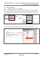
1. Connect user’s system with the E10A-USB emulator connected to PC.
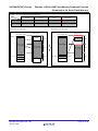
2. Start the High-performance Embedded Workshop to open the work space for user programs.
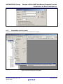
3. The CPU Select dialog box is displayed as shown in Figure 6.1.
Select the CPU in use from the drop-down listbox for Device and click the OK button.
Note: The shown window is an example agopting the SH72673.
Figure 6.1 Device Select Dialog Box
4. The Connecting dialog box is displayed and emulator connection gets started.
The reset signal request dialog box shown in Figure 6.2is displayed.
Figure 6.2 RESET Signal Request Dialog Box
5. Turn on the user’s system.
Having received the RESET signal from the user’s system, click the OK button.
R01AN1151EJ0100 Rev.1.00
Jun.18, 2012
Page 22 of 29
SH7266/SH7267 Groups
Example of E10A-USB Flash Memory Download Function
(Download to the Serial Flash Memory)
When “Connected” is displayed on the Output Window in the High-performance Embedded Workshop, the E10AUSB emulator successfully started.
6.1.2
1.
2.
3.
4.
5.
Registering a Batch File
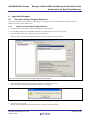
Select in the menu; [Debug] Æ [Debug Settings]
The window shown in Figure 6.3 is open.
Select “Before download modules” in the pull-down menu for the “Command batch file load timing”.
Click the “Add” at “Command line batch processing” to add a batch file.
Click the OK button, and registration is completed.
Figure 6.3 Window for Debug Setting
R01AN1151EJ0100 Rev.1.00
Jun.18, 2012
Page 23 of 29
SH7266/SH7267 Groups
Example of E10A-USB Flash Memory Download Function
(Download to the Serial Flash Memory)
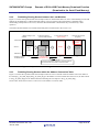
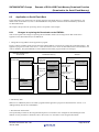
6.1.3
Setting Configuration Dialog Box
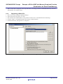
1. Select in the menu; [Setup] Æ [Emulator] Æ [System]
2. Figure 6.4 shows the “Configuration” dialog box (the page of lading flash memory) for setting to download a user
program to the external flash memory using the E10A-USB emulator.
Figure 6.4 Configuration Dialog Box (in the page of loading flash memory)
Table 6.1 lists the setting for each item. When make the settings and click the OK button, configuration is completed.
Table 6.1 Setting Value in the Configuration Dialog Box
Item
Loading flash memory
Erasing flash memory
File Name
Bus width of flash memory
All erasing module address
Writing module address
6.1.4
Setting Value
Enable
Enable
sh7267_sflash_fmtool.mot (the directory which stores the FMTOOL)
32-bit bus width
Specify the start address of erase module (H'FFF8 2000)
Specify the start address of write module (H'FFF8 2100)
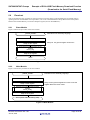
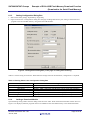
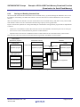
Adding a Download Module
Open the debug setting window from the debug menu and click “Add”. When the download module window shown in
Figure 6.5 is displayed, add user programs which to be loaded into the serial flash memory to the download module.
R01AN1151EJ0100 Rev.1.00
Jun.18, 2012
Page 24 of 29
SH7266/SH7267 Groups
Example of E10A-USB Flash Memory Download Function
(Download to the Serial Flash Memory)
Figure 6.5 Download Module Window
6.1.5
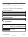
Downloading a User Program
Using the download function shown in Figure 6.6, download the user programs.
Figure 6.6 Downloading User Programs
R01AN1151EJ0100 Rev.1.00
Jun.18, 2012
Page 25 of 29
SH7266/SH7267 Groups
Example of E10A-USB Flash Memory Download Function
(Download to the Serial Flash Memory)
6.2
Application to Serial Flash Boot
In this application note, the function for booting from the serial flash memory is called the “serial flash boot”. For
details on the serial flash boot, refer to “SH7266/SH7267 Groups Boot From the Serial Flash Memory (document
No.:R01AN0214EJ)”.
The sample code provides the processing which corresponds to the example
6.2.1
Changes in replacing the Downloader to the FMTOOL
This section explains the changes in replacing the downloader which is the writing tool for flash of the above
application note (R01AN0214EJ) to the FMTOOL.
1. Change the storing address for the application program
Figure 6.7shows examples of the section allocation and the address conversion for booting the serial flash memory. The
application program is stored in the sector 1 or later because the sector cannot be shared between the load modules. The
value of APROG_TOP_SFLASH Macro which defined in the loader program needs to be changed.
Integrated development
environment
H'FFF8 0000
Loader program
Serial flash memory
H'0000 0000
(Sector 0)
H'FFF8 0000
Loader program
Loader program
FMTOOL
Prohibited
H'0001 0000
(Sector 1)
SH7267
Transmitted by the
internally stored
ROM program
appinfo
Application
program
Transmitted by the
loader program
FMTOOL
H'1C00 0000
appinfo
Application
program
H'1C00 0000
appinfo
Application
progrma
Figure 6.7 Section Allocation and Address Conversion at Booting the Serial Flash
2. Add dummy data
Make sure to add dummy data to the loader program and the application program as described in the section “ 5.9.1
Adding Dummy Data to the Load Module”
3. Download the load module
The operational procedure for the integrated development environment is also changed for downloading the load
module. For the procedure to download, refer to the section “6.1 Procedure of User Program Download”.
R01AN1151EJ0100 Rev.1.00
Jun.18, 2012
Page 26 of 29
SH7266/SH7267 Groups
Example of E10A-USB Flash Memory Download Function
(Download to the Serial Flash Memory)
6.2.2
Storing and Reading Constant Data
The downloader downloads the load module to the serial flash memory by RAM, although the FMTOOL does not use
the RAM for downloading. The FMTOOL enables to store the data which exceeds the RAM limit to the serial flash
memory.
This section describes the method to store the constant data to the serial flash memory and read it locally when needed.
This method is effective for the constant data which has large capacity such as graphic data.
Figure 6.8 shows the operation for storing and reading the constant data. The application program will be implemented
as follows.
-
Declare the const-modified constant data within the section which defined in the unused space such as CS0 space.
-
Do not access to the constant data directly from the variable identifier.
-
Implement the access function of RSPI and read the constant data from the serial flash memory when needed.
Note: The area where the section to be allocated must be registered in the address conversion table.
Load module
(Application program)
Large-capacity internal
RAM space
SH7267
Large-capacity internal
RAM
Serial flash memory
H'0001 0000
Application program
Application program
Transmitted by the loader
program
Application program
RSPI
Unused space
(CS0 space etc.)
Constant data 1
Constant data
H'0010 0000
Constant data 1
Constant data 2
Constant data 2
Constant data 3
Constant data 3
Transmitted by the application
program
Figure 6.8 Operation of Storing and Reading the Constant Data
R01AN1151EJ0100 Rev.1.00
Jun.18, 2012
Page 27 of 29
SH7266/SH7267 Groups
Example of E10A-USB Flash Memory Download Function
(Download to the Serial Flash Memory)
6.3
Customizing FMTOOL
The sample code is dependent on the specification of the device in the serial flash memory. Customization of the
program may be necessary when altering the device.
6.3.1
Device Specification Capable for Sample Code
Table 6.2 and Table 6.3 list the specification of the current device and the commands used in the sample code
respectively.
Table 6.2 Specification of the Current Device
Item
Manufacturer
Model
Capacity
Interface
Access time
Sector structure
Sector size
Page size
Description
Silicon Storage Technology, Inc.
SST25VF016B
2M bytes
Four-wire SPI bus (non-multi I/O bus)
80 MHz
Uniform
64K bytes
256 bytes
Table 6.3 Commands Used in the Sample Code
Item
Erase command
Program command
6.3.2
Description
H'D8 (64KB sector erase)
H'02 (byte programming)
H'AD (auto-increment addressing, word programming)
Contents of Customization
Table 6.4 lists the necessary customizations and the contents.
Table 6.4 Necessary Customization and the Contents
Cases
Improper sector size
(not suitable for 64K-byte sector
area)
Contents
For the Uniform type sector structure, alter the setting value of macro
SF_SECTOR_SIZE to the new sector size. Change the sector erase
command used in R_SF_RSPI_EraseChip function to the command that
supports the new sector size. For the Top or Bottom type structure, the
algorithm to discriminate sector number in fmtool_write function should
also be altered.
Customization is required for the serial flash memory operation function
and the Renesas serial peripheral interface control function. For details,
refer to the sample code.
Different procedure for device
initialization
The command in Table 6.3 is
unusable.
Different electric characteristics.
Note: The FMTOOL is flash memory specification dependent. Therefore the items in Table 6.4 do not cover
all the cases. Check the data sheet and modify the FMTOOL according to the specification in it.
R01AN1151EJ0100 Rev.1.00
Jun.18, 2012
Page 28 of 29
SH7266/SH7267 Groups
Example of E10A-USB Flash Memory Download Function
(Download to the Serial Flash Memory)
7.
Sample Code
The sample code can be downloaded from the Renesas Electronics website.
8.
Reference Documents
Hardware Manual
SH7266 Group, SH7267 Group User’s Manual: Hardware Rev.1.00
(The latest version can be downloaded from the Renesas Electronics website.)
Technical Update/Technical News
(The latest information can be downloaded from the Renesas Electronics website.)
C Complier Manual
SuperH RISC engine C/C++ Compiler, Assembler, Optimizing Linkage Editor
Compiler Package V.9.04 User's Manual
C Complier User’s Manual Rev.1.01
(The latest version can be downloaded from the Renesas Electronics website.)
SuperH Family E10A-USB Emulator User’s Manual Rev.9.00
(The latest version can be downloaded from the Renesas Electronics website.)
Website and Support
Renesas Electronics website
http://www.renesas.com/
Inquiries
http://www.renesas.com/contact/
R01AN1151EJ0100 Rev.1.00
Jun.18, 2012
Page 29 of 29
Revision History
Rev.
1.00
Date
Jun.18, 2012
SH7266/SH7267 Group Application Note E10A-USB Flash Memory
Download Function (Download to Serial Flash Memory)
Page
—
Description
Summary
First edition issued
All trademarks and registered trademarks are the property of their respective owners.
A-1
General Precautions in the Handling of MPU/MCU Products
The following usage notes are applicable to all MPU/MCU products from Renesas. For detailed usage notes on the
products covered by this manual, refer to the relevant sections of the manual. If the descriptions under General
Precautions in the Handling of MPU/MCU Products and in the body of the manual differ from each other, the
description in the body of the manual takes precedence.
1. Handling of Unused Pins
Handle unused pins in accord with the directions given under Handling of Unused Pins in the manual.
⎯ The input pins of CMOS products are generally in the high-impedance state. In operation with an
unused pin in the open-circuit state, extra electromagnetic noise is induced in the vicinity of LSI, an
associated shoot-through current flows internally, and malfunctions occur due to the false
recognition of the pin state as an input signal become possible. Unused pins should be handled as
described under Handling of Unused Pins in the manual.
2. Processing at Power-on
The state of the product is undefined at the moment when power is supplied.
⎯ The states of internal circuits in the LSI are indeterminate and the states of register settings and
pins are undefined at the moment when power is supplied.
In a finished product where the reset signal is applied to the external reset pin, the states of pins
are not guaranteed from the moment when power is supplied until the reset process is completed.
In a similar way, the states of pins in a product that is reset by an on-chip power-on reset function
are not guaranteed from the moment when power is supplied until the power reaches the level at
which resetting has been specified.
3. Prohibition of Access to Reserved Addresses
Access to reserved addresses is prohibited.
⎯ The reserved addresses are provided for the possible future expansion of functions. Do not access
these addresses; the correct operation of LSI is not guaranteed if they are accessed.
4. Clock Signals
After applying a reset, only release the reset line after the operating clock signal has become stable.
When switching the clock signal during program execution, wait until the target clock signal has
stabilized.
⎯ When the clock signal is generated with an external resonator (or from an external oscillator)
during a reset, ensure that the reset line is only released after full stabilization of the clock signal.
Moreover, when switching to a clock signal produced with an external resonator (or by an external
oscillator) while program execution is in progress, wait until the target clock signal is stable.
5. Differences between Products
Before changing from one product to another, i.e. to one with a different type number, confirm that the
change will not lead to problems.
⎯ The characteristics of MPU/MCU in the same group but having different type numbers may differ
because of the differences in internal memory capacity and layout pattern. When changing to
products of different type numbers, implement a system-evaluation test for each of the products.
Notice
1.
Descriptions of circuits, software and other related information in this document are provided only to illustrate the operation of semiconductor products and application examples. You are fully responsible for
the incorporation of these circuits, software, and information in the design of your equipment. Renesas Electronics assumes no responsibility for any losses incurred by you or third parties arising from the
use of these circuits, software, or information.
2.
Renesas Electronics has used reasonable care in preparing the information included in this document, but Renesas Electronics does not warrant that such information is error free. Renesas Electronics
3.
Renesas Electronics does not assume any liability for infringement of patents, copyrights, or other intellectual property rights of third parties by or arising from the use of Renesas Electronics products or
assumes no liability whatsoever for any damages incurred by you resulting from errors in or omissions from the information included herein.
technical information described in this document. No license, express, implied or otherwise, is granted hereby under any patents, copyrights or other intellectual property rights of Renesas Electronics or
others.
4.
You should not alter, modify, copy, or otherwise misappropriate any Renesas Electronics product, whether in whole or in part. Renesas Electronics assumes no responsibility for any losses incurred by you or
5.
Renesas Electronics products are classified according to the following two quality grades: "Standard" and "High Quality". The recommended applications for each Renesas Electronics product depends on
third parties arising from such alteration, modification, copy or otherwise misappropriation of Renesas Electronics product.
the product's quality grade, as indicated below.
"Standard": Computers; office equipment; communications equipment; test and measurement equipment; audio and visual equipment; home electronic appliances; machine tools; personal electronic
equipment; and industrial robots etc.
"High Quality": Transportation equipment (automobiles, trains, ships, etc.); traffic control systems; anti-disaster systems; anti-crime systems; and safety equipment etc.
Renesas Electronics products are neither intended nor authorized for use in products or systems that may pose a direct threat to human life or bodily injury (artificial life support devices or systems, surgical
implantations etc.), or may cause serious property damages (nuclear reactor control systems, military equipment etc.). You must check the quality grade of each Renesas Electronics product before using it
in a particular application. You may not use any Renesas Electronics product for any application for which it is not intended. Renesas Electronics shall not be in any way liable for any damages or losses
incurred by you or third parties arising from the use of any Renesas Electronics product for which the product is not intended by Renesas Electronics.
6.
You should use the Renesas Electronics products described in this document within the range specified by Renesas Electronics, especially with respect to the maximum rating, operating supply voltage
range, movement power voltage range, heat radiation characteristics, installation and other product characteristics. Renesas Electronics shall have no liability for malfunctions or damages arising out of the
use of Renesas Electronics products beyond such specified ranges.
7.
Although Renesas Electronics endeavors to improve the quality and reliability of its products, semiconductor products have specific characteristics such as the occurrence of failure at a certain rate and
malfunctions under certain use conditions. Further, Renesas Electronics products are not subject to radiation resistance design. Please be sure to implement safety measures to guard them against the
possibility of physical injury, and injury or damage caused by fire in the event of the failure of a Renesas Electronics product, such as safety design for hardware and software including but not limited to
redundancy, fire control and malfunction prevention, appropriate treatment for aging degradation or any other appropriate measures. Because the evaluation of microcomputer software alone is very difficult,
please evaluate the safety of the final products or systems manufactured by you.
8.
Please contact a Renesas Electronics sales office for details as to environmental matters such as the environmental compatibility of each Renesas Electronics product. Please use Renesas Electronics
products in compliance with all applicable laws and regulations that regulate the inclusion or use of controlled substances, including without limitation, the EU RoHS Directive. Renesas Electronics assumes
no liability for damages or losses occurring as a result of your noncompliance with applicable laws and regulations.
9.
Renesas Electronics products and technology may not be used for or incorporated into any products or systems whose manufacture, use, or sale is prohibited under any applicable domestic or foreign laws or
regulations. You should not use Renesas Electronics products or technology described in this document for any purpose relating to military applications or use by the military, including but not limited to the
development of weapons of mass destruction. When exporting the Renesas Electronics products or technology described in this document, you should comply with the applicable export control laws and
regulations and follow the procedures required by such laws and regulations.
10. It is the responsibility of the buyer or distributor of Renesas Electronics products, who distributes, disposes of, or otherwise places the product with a third party, to notify such third party in advance of the
contents and conditions set forth in this document, Renesas Electronics assumes no responsibility for any losses incurred by you or third parties as a result of unauthorized use of Renesas Electronics
products.
11. This document may not be reproduced or duplicated in any form, in whole or in part, without prior written consent of Renesas Electronics.
12. Please contact a Renesas Electronics sales office if you have any questions regarding the information contained in this document or Renesas Electronics products, or if you have any other inquiries.
(Note 1)
"Renesas Electronics" as used in this document means Renesas Electronics Corporation and also includes its majority-owned subsidiaries.
(Note 2)
"Renesas Electronics product(s)" means any product developed or manufactured by or for Renesas Electronics.
http://www.renesas.com
SALES OFFICES
Refer to "http://www.renesas.com/" for the latest and detailed information.
Renesas Electronics America Inc.
2880 Scott Boulevard Santa Clara, CA 95050-2554, U.S.A.
Tel: +1-408-588-6000, Fax: +1-408-588-6130
Renesas Electronics Canada Limited
1101 Nicholson Road, Newmarket, Ontario L3Y 9C3, Canada
Tel: +1-905-898-5441, Fax: +1-905-898-3220
Renesas Electronics Europe Limited
Dukes Meadow, Millboard Road, Bourne End, Buckinghamshire, SL8 5FH, U.K
Tel: +44-1628-585-100, Fax: +44-1628-585-900
Renesas Electronics Europe GmbH
Arcadiastrasse 10, 40472 Düsseldorf, Germany
Tel: +49-211-65030, Fax: +49-211-6503-1327
Renesas Electronics (China) Co., Ltd.
7th Floor, Quantum Plaza, No.27 ZhiChunLu Haidian District, Beijing 100083, P.R.China
Tel: +86-10-8235-1155, Fax: +86-10-8235-7679
Renesas Electronics (Shanghai) Co., Ltd.
Unit 204, 205, AZIA Center, No.1233 Lujiazui Ring Rd., Pudong District, Shanghai 200120, China
Tel: +86-21-5877-1818, Fax: +86-21-6887-7858 / -7898
Renesas Electronics Hong Kong Limited
Unit 1601-1613, 16/F., Tower 2, Grand Century Place, 193 Prince Edward Road West, Mongkok, Kowloon, Hong Kong
Tel: +852-2886-9318, Fax: +852 2886-9022/9044
Renesas Electronics Taiwan Co., Ltd.
13F, No. 363, Fu Shing North Road, Taipei, Taiwan
Tel: +886-2-8175-9600, Fax: +886 2-8175-9670
Renesas Electronics Singapore Pte. Ltd.
1 harbourFront Avenue, #06-10, keppel Bay Tower, Singapore 098632
Tel: +65-6213-0200, Fax: +65-6278-8001
Renesas Electronics Malaysia Sdn.Bhd.
Unit 906, Block B, Menara Amcorp, Amcorp Trade Centre, No. 18, Jln Persiaran Barat, 46050 Petaling Jaya, Selangor Darul Ehsan, Malaysia
Tel: +60-3-7955-9390, Fax: +60-3-7955-9510
Renesas Electronics Korea Co., Ltd.
11F., Samik Lavied' or Bldg., 720-2 Yeoksam-Dong, Kangnam-Ku, Seoul 135-080, Korea
Tel: +82-2-558-3737, Fax: +82-2-558-5141
© 2012 Renesas Electronics Corporation. All rights reserved.
Colophon 2.0