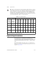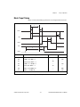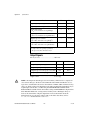
1
DAQ PCI-DIO-96/PXI-6508/PCI-6503 User Manual 96-Bit and 24-Bit Parallel Digital I/O Interface for PCI, PXI, and CompactPCI PCI-DIO-96/PXI-6508/PCI-6503 User Manual March 2009 374938B-01 Support Worldwide Technical Support and Product Information ni.com National Instruments Corporate Headquarters 11500 North Mopac Expressway Austin, Texas 78759-3504 USA Tel: 512 683 0100 Worldwide Offices Australia 1800 300 800, Austria 43 662 457990-0, Belgium 32 (0) 2 757 0020, Brazil 55 11 3262 3599, Canada 800 433 3488, China 86 21 5050 9800, Czech Republic 420 224 235 774, Denmark 45 45 76 26 00, Finland 358 (0) 9 725 72511, France 01 57 66 24 24, Germany 49 89 7413130, India 91 80 41190000, Israel 972 3 6393737, Italy 39 02 41309277, Japan 0120-527196, Korea 82 02 3451 3400, Lebanon 961 (0) 1 33 28 28, Malaysia 1800 887710, Mexico 01 800 010 0793, Netherlands 31 (0) 348 433 466, New Zealand 0800 553 322, Norway 47 (0) 66 90 76 60, Poland 48 22 328 90 10, Portugal 351 210 311 210, Russia 7 495 783 6851, Singapore 1800 226 5886, Slovenia 386 3 425 42 00, South Africa 27 0 11 805 8197, Spain 34 91 640 0085, Sweden 46 (0) 8 587 895 00, Switzerland 41 56 2005151, Taiwan 886 02 2377 2222, Thailand 662 278 6777, Turkey 90 212 279 3031, United Kingdom 44 (0) 1635 523545 For further support information, refer to the Technical Support and Professional Services appendix. To comment on National Instruments documentation, refer to the National Instruments Web site at ni.com/info and enter the info code feedback. © 2006–2009 National Instruments Corporation. All rights reserved. Important Information Warranty The PCI-DIO-96, PXI-6508, and PCI-6503 are warranted against defects in materials and workmanship for a period of one year from the date of shipment, as evidenced by receipts or other documentation. National Instruments will, at its option, repair or replace equipment that proves to be defective during the warranty period. This warranty includes parts and labor. The media on which you receive National Instruments software are warranted not to fail to execute programming instructions, due to defects in materials and workmanship, for a period of 90 days from date of shipment, as evidenced by receipts or other documentation. National Instruments will, at its option, repair or replace software media that do not execute programming instructions if National Instruments receives notice of such defects during the warranty period. National Instruments does not warrant that the operation of the software shall be uninterrupted or error free. A Return Material Authorization (RMA) number must be obtained from the factory and clearly marked on the outside of the package before any equipment will be accepted for warranty work. National Instruments will pay the shipping costs of returning to the owner parts which are covered by warranty. National Instruments believes that the information in this document is accurate. The document has been carefully reviewed for technical accuracy. In the event that technical or typographical errors exist, National Instruments reserves the right to make changes to subsequent editions of this document without prior notice to holders of this edition. The reader should consult National Instruments if errors are suspected. In no event shall National Instruments be liable for any damages arising out of or related to this document or the information contained in it. EXCEPT AS SPECIFIED HEREIN, NATIONAL INSTRUMENTS MAKES NO WARRANTIES, EXPRESS OR IMPLIED, AND SPECIFICALLY DISCLAIMS ANY WARRANTY OF MERCHANTABILITY OR FITNESS FOR A PARTICULAR PURPOSE. CUSTOMER’S RIGHT TO RECOVER DAMAGES CAUSED BY FAULT OR NEGLIGENCE ON THE PART OF NATIONAL INSTRUMENTS SHALL BE LIMITED TO THE AMOUNT THERETOFORE PAID BY THE CUSTOMER. NATIONAL INSTRUMENTS WILL NOT BE LIABLE FOR DAMAGES RESULTING FROM LOSS OF DATA, PROFITS, USE OF PRODUCTS, OR INCIDENTAL OR CONSEQUENTIAL DAMAGES, EVEN IF ADVISED OF THE POSSIBILITY THEREOF. This limitation of the liability of National Instruments will apply regardless of the form of action, whether in contract or tort, including negligence. Any action against National Instruments must be brought within one year after the cause of action accrues. National Instruments shall not be liable for any delay in performance due to causes beyond its reasonable control. The warranty provided herein does not cover damages, defects, malfunctions, or service failures caused by owner’s failure to follow the National Instruments installation, operation, or maintenance instructions; owner’s modification of the product; owner’s abuse, misuse, or negligent acts; and power failure or surges, fire, flood, accident, actions of third parties, or other events outside reasonable control. Copyright Under the copyright laws, this publication may not be reproduced or transmitted in any form, electronic or mechanical, including photocopying, recording, storing in an information retrieval system, or translating, in whole or in part, without the prior written consent of National Instruments Corporation. National Instruments respects the intellectual property of others, and we ask our users to do the same. NI software is protected by copyright and other intellectual property laws. Where NI software may be used to reproduce software or other materials belonging to others, you may use NI software only to reproduce materials that you may reproduce in accordance with the terms of any applicable license or other legal restriction. Trademarks National Instruments, NI, ni.com, and LabVIEW are trademarks of National Instruments Corporation. Refer to the Terms of Use section on ni.com/legal for more information about National Instruments trademarks. Other product and company names mentioned herein are trademarks or trade names of their respective companies. Members of the National Instruments Alliance Partner Program are business entities independent from National Instruments and have no agency, partnership, or joint-venture relationship with National Instruments. Patents For patents covering National Instruments products/technology, refer to the appropriate location: Help»Patents in your software, the patents.txt file on your media, or the National Instruments Patent Notice at ni.com/patents. WARNING REGARDING USE OF NATIONAL INSTRUMENTS PRODUCTS (1) NATIONAL INSTRUMENTS PRODUCTS ARE NOT DESIGNED WITH COMPONENTS AND TESTING FOR A LEVEL OF RELIABILITY SUITABLE FOR USE IN OR IN CONNECTION WITH SURGICAL IMPLANTS OR AS CRITICAL COMPONENTS IN ANY LIFE SUPPORT SYSTEMS WHOSE FAILURE TO PERFORM CAN REASONABLY BE EXPECTED TO CAUSE SIGNIFICANT INJURY TO A HUMAN. (2) IN ANY APPLICATION, INCLUDING THE ABOVE, RELIABILITY OF OPERATION OF THE SOFTWARE PRODUCTS CAN BE IMPAIRED BY ADVERSE FACTORS, INCLUDING BUT NOT LIMITED TO FLUCTUATIONS IN ELECTRICAL POWER SUPPLY, COMPUTER HARDWARE MALFUNCTIONS, COMPUTER OPERATING SYSTEM SOFTWARE FITNESS, FITNESS OF COMPILERS AND DEVELOPMENT SOFTWARE USED TO DEVELOP AN APPLICATION, INSTALLATION ERRORS, SOFTWARE AND HARDWARE COMPATIBILITY PROBLEMS, MALFUNCTIONS OR FAILURES OF ELECTRONIC MONITORING OR CONTROL DEVICES, TRANSIENT FAILURES OF ELECTRONIC SYSTEMS (HARDWARE AND/OR SOFTWARE), UNANTICIPATED USES OR MISUSES, OR ERRORS ON THE PART OF THE USER OR APPLICATIONS DESIGNER (ADVERSE FACTORS SUCH AS THESE ARE HEREAFTER COLLECTIVELY TERMED “SYSTEM FAILURES”). ANY APPLICATION WHERE A SYSTEM FAILURE WOULD CREATE A RISK OF HARM TO PROPERTY OR PERSONS (INCLUDING THE RISK OF BODILY INJURY AND DEATH) SHOULD NOT BE RELIANT SOLELY UPON ONE FORM OF ELECTRONIC SYSTEM DUE TO THE RISK OF SYSTEM FAILURE. TO AVOID DAMAGE, INJURY, OR DEATH, THE USER OR APPLICATION DESIGNER MUST TAKE REASONABLY PRUDENT STEPS TO PROTECT AGAINST SYSTEM FAILURES, INCLUDING BUT NOT LIMITED TO BACK-UP OR SHUT DOWN MECHANISMS. BECAUSE EACH END-USER SYSTEM IS CUSTOMIZED AND DIFFERS FROM NATIONAL INSTRUMENTS' TESTING PLATFORMS AND BECAUSE A USER OR APPLICATION DESIGNER MAY USE NATIONAL INSTRUMENTS PRODUCTS IN COMBINATION WITH OTHER PRODUCTS IN A MANNER NOT EVALUATED OR CONTEMPLATED BY NATIONAL INSTRUMENTS, THE USER OR APPLICATION DESIGNER IS ULTIMATELY RESPONSIBLE FOR VERIFYING AND VALIDATING THE SUITABILITY OF NATIONAL INSTRUMENTS PRODUCTS WHENEVER NATIONAL INSTRUMENTS PRODUCTS ARE INCORPORATED IN A SYSTEM OR APPLICATION, INCLUDING, WITHOUT LIMITATION, THE APPROPRIATE DESIGN, PROCESS AND SAFETY LEVEL OF SUCH SYSTEM OR APPLICATION. Contents About This Manual Conventions ...................................................................................................................ix Related Documentation..................................................................................................x Chapter 1 Introduction About Your Board .........................................................................................................1-1 Using PXI with CompactPCI.........................................................................................1-2 What You Need to Get Started ......................................................................................1-2 Optional Equipment .......................................................................................................1-3 Custom Cabling .............................................................................................................1-3 Unpacking ......................................................................................................................1-4 Chapter 2 Installation and Configuration Software Installation ......................................................................................................2-1 Installing NI-DAQ...........................................................................................2-1 Installing Other Software ................................................................................2-1 Hardware Installation.....................................................................................................2-1 Installing the PCI-DIO-96 or PCI-6503 ..........................................................2-1 Installing the PXI-6508 ...................................................................................2-2 Board Configuration ......................................................................................................2-2 Chapter 3 Signal Connections I/O Connector (PCI-DIO-96, PXI-6508) .......................................................................3-1 I/O Connector Pin Assignments ......................................................................3-1 Cable Assembly Connectors............................................................................3-3 I/O Connector Signal Descriptions..................................................................3-4 I/O Connector (PCI-6503) .............................................................................................3-6 PCI-6503 I/O Connector Pin Descriptions ......................................................3-6 Port C Pin Assignments .................................................................................................3-7 Digital I/O Signal Connections......................................................................................3-8 Power Connections ........................................................................................................3-10 Digital I/O Power-up State Selection.............................................................................3-10 High DIO Power-up State ...............................................................................3-10 Low DIO Power-up State (PXI-6508, PCI-6503 Only) ..................................3-12 © National Instruments Corporation v PCI-DIO-96/PXI-6508/PCI-6503 User Manual Contents Chapter 4 Theory of Operation Functional Overview ..................................................................................................... 4-1 PCI Interface Circuitry.................................................................................... 4-3 82C55A Programmable Peripheral Interface .................................................. 4-3 Timing Specifications.................................................................................................... 4-4 Mode 1 Input Timing ...................................................................................... 4-5 Mode 1 Output Timing ................................................................................... 4-6 Mode 2 Bidirectional Timing.......................................................................... 4-7 Appendix A Specifications Appendix B Register-Level Programming 82C53 Programmable Interval Timer (PCI-DIO-96, PXI-6508 Only) ......................... B-2 Interrupt Control Circuitry .............................................................................. B-2 Register Map and Description ....................................................................................... B-4 Introduction ..................................................................................................... B-4 Register Map ................................................................................................... B-5 Register Descriptions ...................................................................................... B-6 Register Description Format............................................................. B-6 Register Description for the 82C55A ............................................... B-6 Register Description for the 82C53 (PCI-DIO-96, PXI-6508 Only) ...................................................... B-9 Register Description for the Interrupt Control Registers.................. B-10 Interrupt Control Register 1.............................................................. B-10 Interrupt Control Register 2.............................................................. B-12 Interrupt Clear Register (PCI-DIO-96, PXI-6508 Only).................. B-13 Programming ................................................................................................................. B-14 PCl Local Bus ................................................................................................. B-14 Programming Examples.................................................................................. B-14 PCI Initialization............................................................................... B-15 Programming Considerations for the 82C55A................................................ B-17 Modes of Operation .......................................................................... B-17 Mode 0—Basic I/O........................................................................... B-18 Mode 1—Strobed Input .................................................................... B-19 Port C Status-Word Bit Definitions for Input (Ports A and B) ........ B-21 Mode 1—Strobed Output ................................................................. B-23 Port C Status-Word Bit Definitions for Output (Ports A and B)...... B-24 Mode 2—Bidirectional Bus.............................................................. B-26 PCI-DIO-96/PXI-6508/PCI-6503 User Manual vi ni.com Contents Port C Status-Word Bit Definitions for Bidirectional Data Path (Port A Only) .................................................................B-27 Interrupt Handling ...........................................................................................B-29 Interrupt Programming Examples for the 82C55A...........................B-29 Programming Considerations for the 82C53...................................................B-30 General Information ..........................................................................B-30 Interrupt Programming Example ......................................................B-31 Appendix C Technical Support and Professional Services Glossary Index Figures Figure 3-1. Figure 3-2. Figure 3-3. Figure 3-4. Figure 3-5. Figure 3-6. PCI-DIO-96 and PXI-6508 Connector Pin Assignments......................3-2 Cable-Assembly Connector Pinout for the R1005050 Ribbon Cable (PCI-DIO-96 and PXI-6508)..........................................3-3 PCI-6503 I/O Connector Pin Assignments ...........................................3-6 Digital I/O Connections Block Diagram ...............................................3-9 DIO Channel Configured for High DIO Power-up State with External Load .......................................................................3-11 DIO Channel Configured for Low DIO Power-up State with External Load .......................................................................3-12 Figure 4-1. Figure 4-2. Figure 4-3. Figure 4-4. PCI-DIO-96/PXI-6508 Block Diagram.................................................4-2 Timing Specifications for Mode 1 Input Transfer.................................4-5 Timing Specifications for Mode 1 Output Transfer..............................4-6 Timing Specifications for Mode 2 Bidirectional Transfer ....................4-7 Figure B-1. Figure B-2. Figure B-3. Figure B-4. Figure B-5. Figure B-6. Interrupt Control Circuitry Block Diagram...........................................B-3 Control Word Formats for the 82C55A ................................................B-7 Control Word Format for the 82C53 .....................................................B-9 Control Word to Configure Port A for Mode 1 Input ...........................B-19 Control Word to Configure Port B for Mode 1 Input............................B-20 Port C Pin Assignments on I/O Connector when Port C Configured for Mode 1 Input ................................................................B-22 Control Word to Configure Port A for Mode 1 Output.........................B-23 Control Word to Configure Port B for Mode 1 Output.........................B-23 Port C Pin Assignments on I/O Connector when Port C Configured for Mode 1 Output..............................................................B-25 Figure B-7. Figure B-8. Figure B-9. © National Instruments Corporation vii PCI-DIO-96/PXI-6508/PCI-6503 User Manual Contents Figure B-10. Figure B-11. Control Word to Configure Port A as Mode 2 Bidirectional Data Bus .......................................................................... B-26 Port C Pin Assignments on I/O Connector when Port C is Configured for Mode 2 ......................................................................... B-28 Tables Table 3-1. Table 3-2. Table 3-3. Table 4-1. Signal Descriptions for PCI-DIO-96 and PXI-6508 I/O Connectors..................................................................... 3-4 PCI-6503 Signal Descriptions ............................................................. 3-7 Port C Signal Assignments .................................................................. 3-8 Table 4-2. The 82C55A Chips Used in the PCI-DIO-96, PXI-6508, and PCI-6503 ........................................................................................ 4-3 Signal Names Used in Timing Diagrams ............................................. 4-4 Table B-1. Table B-2. Table B-3. Table B-4. Register Address Map .......................................................................... B-5 Port C Set/Reset Control Words .......................................................... B-8 Common Programming Example Terms .............................................. B-15 Mode 0 I/O Configurations .................................................................. B-18 PCI-DIO-96/PXI-6508/PCI-6503 User Manual viii ni.com About This Manual This manual describes the electrical and mechanical aspects of the PCI-DIO-96, PXI-6508, and PCI-6503 and contains information concerning their installation, operation, and programming. The PCI-DIO-96 and PCI-6503 are members of the National Instruments PCI Series of expansion boards for PCI bus computers. The PXI-6508 is a member of the National Instruments PXI family of expansion boards for PXI and CompactPCI chassis. These boards are designed for high-performance data acquisition and control for applications in laboratory testing, production testing, and industrial process monitoring and control. Conventions The following conventions are used in this manual: <> Angle brackets that contain numbers separated by an ellipsis represent a range of values associated with a bit or signal name—for example, AO <3..0>. » The » symbol leads you through nested menu items and dialog box options to a final action. The sequence File»Page Setup»Options directs you to pull down the File menu, select the Page Setup item, and select Options from the last dialog box. This icon to the left of bold italicized text denotes a note, which alerts you to important information. This icon to the left of bold italicized text denotes a caution, which advises you of precautions to take to avoid injury, data loss, or a system crash. bold Bold text denotes items that you must select or click in the software, such as menu items and dialog box options. Bold text also denotes parameter names. italic Italic text denotes variables, emphasis, a cross-reference, or an introduction to a key concept. Italic text also denotes text that is a placeholder for a word or value that you must supply. © National Instruments Corporation ix PCI-DIO-96/PXI-6508/PCI-6503 User Manual About This Manual monospace Text in this font denotes text or characters that you should enter from the keyboard, sections of code, programming examples, and syntax examples. This font is also used for the proper names of disk drives, paths, directories, programs, subprograms, subroutines, device names, functions, operations, variables, filenames, and extensions. PPI x PPI x, where the x is replaced by A, B, C, or D, refers to one of the four programmable peripheral interface (PPI) chips on the PCI-DIO-96 or PXI-6508. The PCI-6503 contains only one PPI, PPI A. Your DIO board Your DIO board refers to either the PCI-DIO-96, PXI-6508, or PCI-6503 board. Related Documentation The following National Instruments document contains information that you may find helpful as you read this manual. • Field Wiring and Noise Considerations for Analog Signals—To access this document, go to ni.com/info and enter the info code rdfwin. • PCI Local Bus Specification, Revision 2.1 • National Instruments PXI Specification, Revision 1.0 • PICMG 2.0 R2.1 CompactPCI • Software documentation—Examples of software documentation you may have are the LabVIEW or LabWindows™/CVI™ documentation sets and the NI-DAQmx or Traditional NI-DAQ (Legacy) documentation. After you set up your hardware system, use either the application software or the NI-DAQ documentation to help you write your application. If you have a large and complicated system, it is worthwhile to look through the software documentation before you configure your hardware. • Accessory installation guides or manuals—If you are using accessory products, read the terminal block and cable assembly installation guides or accessory board user manuals. They explain how to physically connect the relevant pieces of the system. Consult these guides when you are making your connections. PCI-DIO-96/PXI-6508/PCI-6503 User Manual x ni.com 1 Introduction This chapter describes the PCI-DIO-96, PXI-6508, and PCI-6503; lists what you need to get started, software programming choices, and optional equipment; describes custom cabling options; and explains how to unpack your board. About Your Board Thank you for purchasing a National Instruments PCI-DIO-96, PXI-6508, or PCI-6503 board. The PCI-DIO-96 is a 96-bit, parallel, digital I/O interface for PCI bus computers. The PXI-6508 is a 96-bit, parallel, digital I/O interface for PXI and CompactPCI chassis. The PCI-6503 is a 24-bit, parallel, digital I/O interface for PCI bus computers. Four 82C55A programmable peripheral interface (PPI) chips control the 96 bits of TTL-compatible digital I/O on the PCI-DIO-96 or PXI-6508. On the PCI-6503, one 82C55A PPI controls the 24 bits of TTL-compatible digital I/O. The 82C55A PPI chips can operate in unidirectional mode, bidirectional mode, or handshaking mode and can generate interrupt requests to your computer. The digital I/O lines are all accessible through a 100-pin female connector on the PCI-DIO-96 or PXI-6508 and a 50-pin male connector on the PCI-6503. Your DIO board is a completely switchless and jumperless DAQ board. All resource allocation is completed automatically at startup, so you will not need to set interrupt levels or base addresses. With your DIO board, you can use your computer as a digital I/O system controller for laboratory testing, production testing, and industrial process monitoring and control. Detailed PCI-DIO-96, PXI-6508, and PCI-6503 specifications are in Appendix A, Specifications. © National Instruments Corporation 1-1 PCI-DIO-96/PXI-6508/PCI-6503 User Manual Chapter 1 Introduction Using PXI with CompactPCI Using PXI-compatible products with standard CompactPCI products is an important feature provided by the PXI Specification, Revision 1.0. If you use a PXI-compatible plug-in device in a standard CompactPCI chassis you can use the basic plug-in device functions, but the PXI-specific functions will be unavailable. The CompactPCI specification permits vendors to develop sub-buses that coexist with the basic PCI interface on the CompactPCI bus. Compatible operation is not guaranteed between CompactPCI devices with different sub-buses nor between CompactPCI devices with sub-buses and PXI. The standard implementation for CompactPCI does not include these sub-buses. Your PXI-6508 device works in any standard CompactPCI chassis adhering to the PICMG 2.0 R2.1 CompactPCI core specification. What You Need to Get Started To set up and use your PCI-DIO-96/PXI-6508/PCI-6503 board, you will need the following: ❑ PCI-DIO-96, PXI-6508, or PCI-6503 board ❑ PCI-DIO-96/PXI-6508/PCI-6503 User Manual ❑ One of the following software packages and documentation: – LabVIEW – LabWindows/CVI – NI-DAQmx – Traditional NI-DAQ (Legacy) – Measurement Studio ❑ Your computer, or PXI or CompactPCI chassis and controller PCI-DIO-96/PXI-6508/PCI-6503 User Manual 1-2 ni.com Chapter 1 Introduction Optional Equipment National Instruments offers a variety of products to use with your DIO board, including cables, connector blocks, and other accessories, as follows: • Cables and cable assemblies • Connector blocks, 50-pin screw terminals • SCXI modules and accessories for isolating, amplifying, exciting, and multiplexing signals for relays and analog output. With SCXI you can condition and acquire up to 3,072 channels. • Low channel count signal conditioning modules, boards, and accessories, including conditioning for strain gauges and RTDs, simultaneous sample and hold, and relays For more information about optional equipment available from National Instruments, visit ni.com. Custom Cabling Caution For compliance with Electromagnetic Compatibility (EMC) requirements, this product must be operated with shielded cables and accessories. If unshielded cables or accessories are used, the EMC specifications are no longer guaranteed unless all unshielded cables and/or accessories are installed in a shielded enclosure with properly designed and shielded input/output ports. National Instruments offers cables and accessories for you to prototype your application or to use if you frequently change board interconnections. If you want to develop your own cable, the mating connector for the PCI-DIO-96 and PXI-6508 is a 100-position, right-angle receptacle without board locks. Recommended manufacturer part numbers for this mating connector are as follows: • AMP Corporation (part number 749879-9) • Honda Corporation (part number PCS-XE100LFD-HS) © National Instruments Corporation 1-3 PCI-DIO-96/PXI-6508/PCI-6503 User Manual Chapter 1 Introduction The mating connector for the PCI-6503 is a 50-position, polarized ribbon socket connector with strain relief. National Instruments uses a polarized (keyed) connector to prevent inadvertent upside-down connections. Recommended manufacturer part numbers for this mating connector are as follows: • Electronic Products Division/3M (part number 3425-7650) • T&B/Ansley Corporation (part number 622-5041) Unpacking Your DIO board is shipped in an antistatic package to prevent electrostatic damage to the board. Electrostatic discharge can damage several components on the board. To avoid such damage in handling the board, take the following precautions: • Ground yourself via a grounding strap or by holding a grounded object. • Touch the antistatic package to a metal part of your computer chassis before removing the board from the package. • Remove the board from the package and inspect the board for loose components or any other sign of damage. Notify National Instruments if the board appears damaged in any way. Do not install a damaged board into your computer. • Never touch the exposed pins of connectors. PCI-DIO-96/PXI-6508/PCI-6503 User Manual 1-4 ni.com Installation and Configuration 2 This chapter describes how to install and configure your PCI-DIO-96, PXI-6508, or PCI-6503 board. Software Installation Before installing your DIO device, you must install the software you plan to use with the device. If you are a register-level programmer, refer to Appendix B, Register-Level Programming, of this manual. Installing NI-DAQ The DAQ Getting Started Guide, which you can download at ni.com/ manuals, offers NI-DAQ users step-by-step instructions for installing software and hardware, configuring channels and tasks, and getting started developing an application. Installing Other Software If you are using other software, refer to the installation instructions that accompany your software. Hardware Installation The following sections contain general installation instructions for each device. Consult your computer or chassis user manual or technical reference manual for specific instructions about installing new devices in your computer or chassis. Installing the PCI-DIO-96 or PCI-6503 To install a PCI-DIO-96 or PCI-6503 in any available 5 V PCI expansion slot in your computer, complete the following steps: 1. Turn off and unplug your computer. 2. Remove the top cover or access port to the expansion slots. © National Instruments Corporation 2-1 PCI-DIO-96/PXI-6508/PCI-6503 User Manual Chapter 2 Installation and Configuration 3. Remove the expansion slot cover on the back panel of the computer. 4. Touch the metal part inside your computer to discharge any static electricity that might be on your clothes or body. 5. Insert the PCI-DIO-96 or PCI-6503 in a 5 V PCI slot. It may be a tight fit, but do not force the device into place. 6. Screw the mounting bracket of the PCI-DIO-96 or PCI-6503 to the back panel rail of the computer. 7. Visually verify the installation. 8. Replace the top cover of your computer. 9. Plug in and turn on your computer. Installing the PXI-6508 To install a PXI-6508 in any available 5 V peripheral slot in your PXI or CompactPCI chassis, complete the following steps: 1. Turn off and unplug your PXI or CompactPCI chassis. 2. Choose an unused PXI or CompactPCI 5 V peripheral slot. 3. Remove the filler panel for the peripheral slot you have chosen. 4. Touch a metal part of your chassis to discharge any static electricity that might be on your clothes or body. 5. Insert the PXI-6508 in the selected 5 V slot. Use the injector/ejector handle to fully inject the device into place. 6. Screw the front panel of the PXI-6508 to the front panel mounting rails of the PXI or CompactPCI chassis. 7. Visually verify the installation. 8. Plug in and turn on the PXI or CompactPCI chassis. Board Configuration Your DIO board is completely software configurable. The PCI-DIO-96 and PCI-6503 are fully compliant with the PCI Local Bus Specification, Revision 2.1, and the PXI-6508 is fully compliant with the PXI Specification, Revision 1.0. Therefore, all board resources are automatically allocated by the PCI system, including the base address and interrupt level. The base address of the board is mapped into PCI memory space. You do not need to perform any configuration steps after the system powers up. PCI-DIO-96/PXI-6508/PCI-6503 User Manual 2-2 ni.com 3 Signal Connections This chapter describes how to make input and output signal connections to your PCI-DIO-96, PXI-6508, and PCI-6503 via the board I/O connector. Caution Connections that exceed any of the maximum ratings of input or output signals on your DIO board can damage the board and your computer. The description of each signal in this chapter includes information about maximum input ratings. National Instruments is not liable for any damages resulting from signal connections that exceed these maximum ratings. For information on adding signal conditioning into your applications and National Instruments signal conditioning devices, go to ni.com/signalconditioning. Note I/O Connector (PCI-DIO-96, PXI-6508) The I/O connector for the PCI-DIO-96 and PXI-6508 has 100 pins that you can connect to 50-pin accessories with the R1005050 cable. I/O Connector Pin Assignments Figure 3-1 shows the pin assignments for the PCI-DIO-96 and PXI-6508 digital I/O connector. © National Instruments Corporation 3-1 PCI-DIO-96/PXI-6508/PCI-6503 User Manual Chapter 3 Signal Connections GND +5 V DPA0 CPA0 DPA1 CPA1 DPA2 CPA2 DPA3 CPA3 DPA4 CPA4 DPA5 CPA5 DPA6 CPA6 DPA7 CPA7 DPB0 CPB0 DPB1 CPB1 DPB2 CPB2 DPB3 CPB3 DPB4 CPB4 DPB5 CPB5 DPB6 CPB6 DPB7 CPB7 DPC0 CPC0 DPC1 CPC1 DPC2 CPC2 DPC3 CPC3 DPC4 CPC4 DPC5 CPC5 DPC6 CPC6 DPC7 CPC7 100 99 98 97 96 95 94 93 92 91 90 89 88 87 86 85 84 83 82 81 80 79 78 77 76 75 74 73 72 71 70 69 68 67 66 65 64 63 62 61 60 59 58 57 56 55 54 53 52 51 50 49 48 47 46 45 44 43 42 41 40 39 38 37 36 35 34 33 32 31 30 29 28 27 26 25 24 23 22 21 20 19 18 17 16 15 14 13 12 11 10 9 8 7 6 5 4 3 2 1 GND +5 V BPA0 APA0 BPA1 APA1 BPA2 APA2 BPA3 APA3 BPA4 APA4 BPA5 APA5 BPA6 APA6 BPA7 APA7 BPB0 APB0 BPB1 APB1 BPB2 APB2 BPB3 APB3 BPB4 APB4 BPB5 APB5 BPB6 APB6 BPB7 APB7 BPC0 APC0 BPC1 APC1 BPC2 APC2 BPC3 APC3 BPC4 APC4 BPC5 APC5 BPC6 APC6 BPC7 APC7 Figure 3-1. PCI-DIO-96 and PXI-6508 Connector Pin Assignments PCI-DIO-96/PXI-6508/PCI-6503 User Manual 3-2 ni.com Chapter 3 Signal Connections Cable Assembly Connectors The optional R1005050 cable assembly you can use with the PCI-DIO-96 or PXI-6508 is an assembly of two 50-pin cables and three connectors. Both cables are joined to a single connector on one end and to individual connectors on the free ends. The 100-pin connector that joins the two cables plugs into the I/O connector of the PCI-DIO-96 and PXI-6508. The other two connectors are 50-pin connectors, one of which is connected to pins 1 through 50 and the other connected to pins 51 through 100 of the PCI-DIO-96 and PXI-6508 connector. Figure 3-2 shows the pin assignments for each of the 50-pin connectors on the cable assembly. Positions 1–50 APC7 APC6 APC5 APC4 APC3 APC2 APC1 APC0 APB7 APB6 APB5 APB4 APB3 APB2 APB1 APB0 APA7 APA6 APA5 APA4 APA3 APA2 APA1 APA0 +5 V 1 3 5 7 9 11 13 15 17 19 21 23 25 27 29 31 33 35 37 39 41 43 45 47 49 2 4 6 8 10 12 14 16 18 20 22 24 26 28 30 32 34 36 38 40 42 44 46 48 50 Positions 51–100 BPC7 CPC7 BPC6 CPC6 BPC5 CPC5 BPC4 CPC4 BPC3 CPC3 BPC2 CPC2 BPC1 CPC1 BPC0 CPC0 BPB7 CPB7 BPB6 CPB6 BPB5 CPB5 BPB4 CPB4 BPB3 CPB3 BPB2 CPB2 BPB1 CPB1 BPB0 CPB0 BPA7 CPA7 BPA6 CPA6 BPA5 CPA5 BPA4 CPA4 BPA3 CPA3 BPA2 CPA2 BPA1 CPA1 BPA0 CPA0 GND +5 V 1 3 5 7 9 11 13 15 17 19 21 23 25 27 29 31 33 35 37 39 41 43 45 47 49 2 4 6 8 10 12 14 16 18 20 22 24 26 28 30 32 34 36 38 40 42 44 46 48 50 DPC7 DPC6 DPC5 DPC4 DPC3 DPC2 DPC1 DPC0 DPB7 DPB6 DPB5 DPB4 DPB3 DPB2 DPB1 DPB0 DPA7 DPA6 DPA5 DPA4 DPA3 DPA2 DPA1 DPA0 GND Figure 3-2. Cable-Assembly Connector Pinout for the R1005050 Ribbon Cable (PCI-DIO-96 and PXI-6508) © National Instruments Corporation 3-3 PCI-DIO-96/PXI-6508/PCI-6503 User Manual Chapter 3 Signal Connections I/O Connector Signal Descriptions Table 3-1 lists the signal descriptions for the PCI-DIO-96 and PXI-6508 I/O connector pins. Table 3-1. Signal Descriptions for PCI-DIO-96 and PXI-6508 I/O Connectors Pin Alternate Port ID† Signal Name Description 1, 3, 5, 7, 9, 11, 13, 15 APC<7..0> 2 Bidirectional data lines for port C of PPI A—APC7 is the MSB, APC0 is the LSB. 2, 4, 6, 8, 10, 12, 14, 16 BPC<7..0> 5 Bidirectional data lines for port C of PPI B—BPC7 is the MSB, BPC0 is the LSB. 17, 19, 21, 23, 25, 27, 29, 31 APB<7..0> 1 Bidirectional data lines for port B of PPI A—APB7 is the MSB, APB0 is the LSB. 18, 20, 22, 24, 26, 28, 30, 32 BPB<7..0> 4 Bidirectional data lines for port B of PPI B—BPB7 is the MSB, BPB0 is the LSB. 33, 35, 37, 39, 41, 43, 45, 47 APA<7..0> 0 Bidirectional data lines for port A of PPI A—APA7 is the MSB, APA0 is the LSB. 34, 36, 38, 40, 42, 44, 46, 48 BPA<7..0> 3 Bidirectional data lines for port A of PPI B—BPA7 is the MSB, BPA0 is the LSB. 49, 99 +5 V supply — +5 Volts—These pins are fused for up to 1 A total of +4.65 to +5.25 V. 50, 100 GND — Ground—These pins are connected to the computer ground signal. 51, 53, 55, 57, 59, 61, 63, 65 CPC<7..0> 8 Bidirectional data lines for port C of PPI C—CPC7 is the MSB, CPC0 is the LSB. 52, 54, 56, 58, 60, 62, 64, 66 DPC<7..0> 11 Bidirectional data lines for port C of PPI D—DPC7 is the MSB, DPC0 is the LSB. PCI-DIO-96/PXI-6508/PCI-6503 User Manual 3-4 ni.com Chapter 3 Signal Connections Table 3-1. Signal Descriptions for PCI-DIO-96 and PXI-6508 I/O Connectors (Continued) Pin Alternate Port ID† Signal Name Description 67, 69, 71, 73, 75, 77, 79, 81 CPB<7..0> 7 Bidirectional data lines for port B of PPI C—CPB7 is the MSB, CPB0 is the LSB. 68, 70, 72, 74, 76, 78, 80, 82 DPB<7..0> 10 Bidirectional data lines for port B of PPI D—DPB7 is the MSB, DPB0 is the LSB. 83, 85, 87, 89, 91, 93, 95, 97 CPA<7..0> 6 Bidirectional data lines for port A of PPI C—CPA7 is the MSB, CPA0 is the LSB. 84, 86, 88, 90, 92, 94, 96, 98 DPA<7..0> 9 Bidirectional data lines for port A of PPI D—DPA7 is the MSB, DPA0 is the LSB. † This document refers to the ports as A, B, and C and the PPIs (82C55As) as A, B, C, and D. NI-DAQmx, Traditional NI-DAQ (Legacy), and LabVIEW documentation use numbers to identify each port and PPI. For example, this manual uses PPI A port A to refer to port A of the 82C55A identified as PPI A. NI-DAQmx, Traditional NI-DAQ (Legacy), LabWindows/CVI, LabVIEW, or other application software documentation, however, refer to this port as 0. The Alternate Port ID column shows the correlation between the different port names. © National Instruments Corporation 3-5 PCI-DIO-96/PXI-6508/PCI-6503 User Manual Chapter 3 Signal Connections I/O Connector (PCI-6503) The PCI-6503 has 50 pins that you can connect to 50-pin accessories with the NB1 cable. PCI-6503 I/O Connector Pin Descriptions Figure 3-3 shows the pin assignments for the PCI-6503 digital I/O connector using the NB1 ribbon cable. PC6 PC5 1 3 5 2 4 6 GND PC4 PC3 7 8 GND 9 11 13 15 17 19 21 23 25 27 29 31 33 35 37 39 10 12 14 16 18 20 22 24 26 28 30 32 34 36 38 40 GND 42 44 46 48 GND GND PA1 PA0 41 43 45 47 +5 V 49 50 PC7 PC2 PC1 PC0 PB7 PB6 PB5 PB4 PB3 PB2 PB1 PB0 PA7 PA6 PA5 PA4 PA3 PA2 GND GND GND GND GND GND GND GND GND GND GND GND GND GND GND GND GND GND GND GND Figure 3-3. PCI-6503 I/O Connector Pin Assignments PCI-DIO-96/PXI-6508/PCI-6503 User Manual 3-6 ni.com Chapter 3 Signal Connections Table 3-2 describes the PCI-6503 signals. Table 3-2. PCI-6503 Signal Descriptions Pin Alternate Port ID† Signal Name Description 1, 3, 5, 7, 9, 11, 13, 15 PC<7..0> 2 Port C—Bidirectional data lines for port C. PC7 is the MSB, PC0 is the LSB. 17, 19, 21, 23, 25, 27, 29, 31 PB<7..0> 1 Port B—Bidirectional data lines for port B. PB7 is the MSB, PB0 is the LSB. 33, 35, 37, 39, 41, 43, 45, 47 PA<7..0> 0 Port A—Bidirectional data lines for port B. PA7 is the MSB, PA0 is the LSB. 49 +5 V — +5 Volts—This pin is fused for up to 1 A at +4.65 to 5.25 V. All even-numbered pins GND — Ground—These signals are connected to the computer ground reference. † This document refers to the 82C55 ports as A, B, and C. NI-DAQmx, Traditional NI-DAQ (Legacy), and LabVIEW documentation use numbers to identify ports. For example, this manual uses port A to refer to the first port of the 82C55A. NI-DAQmx, Traditional NI-DAQ (Legacy), LabWindows/CVI, LabVIEW, or other application software documentation, however, refer to this port as 0. The Alternate Port ID column shows the correlation between the different port names. Port C Pin Assignments The signals assigned to port C vary depending on how the 82C55A is configured. In mode 0—or no handshaking configuration—port C is configured as two 4-bit I/O ports. In modes 1 and 2—or handshaking configuration—port C is used for status and handshaking signals with any leftover lines available for general-purpose I/O. Table 3-3 summarizes the port C signal assignments for each configuration. You can also use ports A and B in different modes; the table does not show every possible combination. Consult Appendix B, Register-Level Programming, for register-level programming information. © National Instruments Corporation 3-7 PCI-DIO-96/PXI-6508/PCI-6503 User Manual Chapter 3 Signal Connections Table 3-3 shows both the port C signal assignments and the terminology correlation between different documentation sources. The 82C55A terminology refers to the different 82C55A configurations as modes whereas NI-DAQmx, Traditional NI-DAQ (Legacy), LabWindows/CVI, and LabVIEW documentation refers to them as handshaking and no handshaking. On the PCI-DIO-96 and PXI-6508, these signal assignments are the same for all four 82C55A PPIs. Refer to Table 3-1 for more information. Note Table 3-3. Port C Signal Assignments Configuration Terminology 82C55A/ PCI-DIO-96/ PXI-6508/ PCI-6503 User Manual Signal Assignments National Instruments Software APC7, BPC7, CPC7, or DPC7 APC6, BPC6, CPC6, or DPC6 APC5, BPC5, CPC5, or DPC5 APC4, BPC4, CPC4, or DPC4 APC3, BPC3, CPC3, or DPC3 APC2, BPC2, CPC2, or DPC2 APC1, BPC1, CPC1, or DPC1 APC0, BPC0, CPC0, or DPC0 Mode 0 (Basic I/O) No Handshaking I/O I/O I/O I/O I/O I/O I/O I/O Mode 1 (Strobed Input) Handshaking I/O I/O IBFA STBA* INTRA STBB* IBFBB INTRB Mode 1 (Strobed Output) Handshaking OBFA* ACKA* I/O I/O INTRA ACKB* OBFB* INTRB Mode 2 (Bidirectional Bus) Handshaking OBFA* ACKA* IBFA STBA* INTRA I/O I/O I/O Notes: Indicates that the signal is active low. Subscripts A and B denote port A or port B handshaking signals. Digital I/O Signal Connections Pins 1 through 48 and, on the PCI-DIO-96 and PXI-6508, pins 51 through 98 of the I/O connector are digital I/O signal pins. The following specifications and ratings apply to the digital I/O lines. The maximum input logic high and output logic high voltages assume a Vcc supply voltage of 5.0 V. The absolute maximum voltage rating is −0.5 to +5.5 V with respect to GND. For more information on the digital I/O signal specifications, refer to Appendix A, Specifications. PCI-DIO-96/PXI-6508/PCI-6503 User Manual 3-8 ni.com Chapter 3 Signal Connections Figure 3-4 depicts signal connections for three typical digital I/O applications. +5 V LED 41 43 Port A 45 PA<3..0> 47 67 69 Port B 71 PB<7..4> TTL Signal 73 +5 V Switch 50, 100 GND I/O Connector DIO Board Figure 3-4. Digital I/O Connections Block Diagram In Figure 3-4, port A of one PPI is configured for digital output, and port B is configured for digital input. Digital input applications include receiving TTL signals and sensing external device states such as the state of the switch in Figure 3-4. Digital output applications include sending TTL signals and driving external devices such as the LED shown in Figure 3-4. © National Instruments Corporation 3-9 PCI-DIO-96/PXI-6508/PCI-6503 User Manual Chapter 3 Signal Connections Power Connections Pin 49 and, on the PCI-DIO-96 and PXI-6508, pin 99 of the I/O connector supply +5 V from the computer power supply via a self-resetting fuse. The fuse resets automatically within a few seconds after the overcurrent condition is removed. These pins are referenced to GND and can be used to power external digital circuitry. Power rating.................................... 1 A at +4.65 to +5.25 V Caution Never connect the +5 V power pins directly to ground or to any other voltage source on your DIO board or to any other device. Doing so can damage your DIO board and the computer. National Instruments is not liable for damage resulting from such a connection. Digital I/O Power-up State Selection The PCI-DIO-96, PXI-6508, and PCI-6503 contain bias resistors that control the state of the digital I/O lines at power up. At power up, each digital I/O line is configured as an input, pulled either high or low by a 100 kΩ bias resistor. On the PCI-DIO-96, all of the 100 kΩ bias resistors pull up. Therefore, the default power-up state of each line on the PCI-DIO-96 is high. On the PXI-6508 and PCI-6503, you can select the direction of the 100 kΩ bias resistors. Set jumper W1 to high to configure the resistors as pull-up resistors. Set jumper W1 to low to configure the resistors as pull-down resistors. You can change individual lines from pulled up to pulled down—or, on the PXI-6508 and PCI-6503, from pulled down to pulled up—by adding your own external resistors. This section describes the procedure. High DIO Power-up State If you select the pulled-high mode, each DIO line is pulled to Vcc (approximately +5 VDC) with a 100 kΩ resistor. To pull a specific line low, connect between that line and ground a pull-down resistor (RL) whose value will give you a maximum of 0.4 VDC. The DIO lines provide a maximum of 2.5 mA at 3.7 V in the high state. Using the largest possible resistor ensures that you do not use more current than necessary to perform the pull-down task. PCI-DIO-96/PXI-6508/PCI-6503 User Manual 3-10 ni.com Chapter 3 Signal Connections However, ensure the resistor value is not so large that leakage current from the DIO line along with the current from the 100 kΩ pull-up resistor drives the voltage at the resistor above a TTL low level of 0.4 VDC. +5 V DIO Board 100 kΩ Digital I/O Line 82C55 RL GND Figure 3-5. DIO Channel Configured for High DIO Power-up State with External Load Example: By default, all DIO lines are pulled high at power up. To pull one channel low, complete the following steps: 1. Install a load (RL). Remember that the smaller the resistance, the greater the current consumption and the lower the voltage. 2. Using the following formula, calculate the largest possible load to maintain a logic low level of 0.4 V and supply the maximum driving current: V = I × RL RL = V/I, where V = 0.4 V; Voltage across RL I = 46 μA + 10 μA; 4.6 V across the 100 kΩ pull-up resistor and 10 μA maximum leakage current(except lines PC0 and PC3) therefore RL = 7.1 kΩ; 0.4 V/56 μA This resistor value, 7.1 kΩ, provides a maximum of 0.4 V on the DIO line at power up. You can substitute smaller resistor values to lower the voltage or to provide a margin for Vcc variations and other factors. However, smaller values draw more current, leaving less drive current for other circuitry connected to this line. The 7.1 kΩ resistor reduces the amount of logic high source current by 0.4 mA with a 2.8 V output. The maximum leakage current on most lines is 10 μA. The maximum leakage current on the PC(0) and PC(3) lines is 20 μA. © National Instruments Corporation 3-11 PCI-DIO-96/PXI-6508/PCI-6503 User Manual Chapter 3 Signal Connections Low DIO Power-up State (PXI-6508, PCI-6503 Only) If you select pulled-low mode, each DIO line will be pulled to GND (0 VDC) using a 100 kΩ resistor. If you want to pull a specific line high, connect a pull-up resistor that will give you a minimum of 2.8 VDC. The DIO lines are capable of sinking a maximum of 2.5 mA at 0.4 V in the low state. Using the largest possible resistance value ensures that you do not use more current than necessary to perform the pull-up task. Also, ensure the pull-up resistor value is not so large that leakage current from the DIO line along with the current from the 100 kΩ pull-down resistor brings the voltage at the resistor below a TTL high level of 2.8 VDC. +5 V DIO Board RL Digital I/O Line 82C55 100 kΩ GND Figure 3-6. DIO Channel Configured for Low DIO Power-up State with External Load Example: Set jumper W1 to low, which means all DIO lines are pulled low at power up. To pull one channel high, complete the following steps: 1. Install a load (RL). Remember that the smaller the resistance, the greater the current consumption and the higher the voltage. 2. Using the following formula, calculate the largest possible load to maintain a logic high level of 2.8 V and supply the maximum sink current: V = I × RL RL = V/I where V = 2.2 V; Voltage across RL I = 28 μA + 10 μA; 2.8 V across the 100 kΩ pull-up resistor and 10 μA maximum leakage current (except lines PC0 and PC3) therefore PCI-DIO-96/PXI-6508/PCI-6503 User Manual RL = 5.7 kΩ; 2.2 V/38 μA 3-12 ni.com Chapter 3 Signal Connections This resistor value, 5.7 kΩ, provides a maximum of 2.8 V on the DIO line at power up. You can substitute smaller resistor values to lower the voltage drop or to provide a margin for VCC variations and other factors. However, smaller values draw more current, leaving less sink current for other circuitry connected to this line. The 5.7 kΩ resistor reduces the amount of a logic low sink current by 0.8 mA with a 0.4 V output. © National Instruments Corporation 3-13 PCI-DIO-96/PXI-6508/PCI-6503 User Manual 4 Theory of Operation This chapter contains a functional overview of the PCI-DIO-96, PXI-6508, and PCI-6503 and explains the operation of each functional unit. Functional Overview The block diagram in Figure 4-1 illustrates the key functional components of your DIO board. © National Instruments Corporation 4-1 PCI-DIO-96/PXI-6508/PCI-6503 User Manual Theory of Operation Data/Address 82C55A PPI A 37 Interface Control 6 Error Reporting 2 Arbitration PCI MITE Interface Circuitry Data Bus 82C55A PPI B PCI or PXI 2 System 2 82C55A PPI C Interrupt 1 Interrupt Interrupt Control Circuitry 82C55A PPI D Interrupt Bus Port A 8 Port B 8 Port C 8 Port A 8 Port B 8 Port C 8 Port A 8 Port B 8 Port C 8 Port A 8 Port B 8 Port C 8 I/O Connector Chapter 4 82C53 Timer PCI-DIO-96/PXI-6508 Only +5 VDC 1 A Fuse Note: Current revisions of the NI PCI-DIO-96 and PXI-6508 no longer support the OKI 82C53 programmable interval timer. If you are using a PCI-DIO-96 revision G or earlier or PXI-6508 revision D or earlier, refer to Appendix B, Register-Level Programming, for more information about using the 82C53. Figure 4-1. PCI-DIO-96/PXI-6508 Block Diagram PCI-DIO-96/PXI-6508/PCI-6503 User Manual 4-2 ni.com Chapter 4 Theory of Operation PCI Interface Circuitry Your DIO board uses the PCI MITE ASIC to communicate with the PCI bus. The PCI MITE ASIC was designed by National Instruments specifically for data acquisition. The PCI MITE is fully compliant with PCI Local Bus Specification, Revision 2.1. The base memory address and interrupt level for the board are stored inside the PCI MITE at power on. You do not need to set any switches or jumpers. 82C55A Programmable Peripheral Interface The 82C55A PPI chip is the heart of your DIO board. The PCI-DIO-96 and PXI-6508 contain four PPIs. The PCI-6503 contains one PPI. Each of these chips has 24 programmable I/O pins that represent three 8-bit ports: PA, PB, and PC. Each port can be programmed as an input or output port. The 82C55A has three modes of operation: simple I/O (mode 0), strobed I/O (mode 1), and bidirectional I/O (mode 2). In modes 1 and 2, the three ports are divided into two groups: group A and group B. Each group has eight data bits, plus control and status bits from port C (PC). Modes 1 and 2 use handshaking signals from the computer to synchronize data transfers. Refer to Appendix B, Register-Level Programming, for more detailed information. Different revisions of the PCI-DIO-96, PXI-6508, and PCI-6503 use different 82C55A chips from Intersil Corporation or OKI Semiconductor. For the most recent data sheet for the Intersil CMS82C55A or CS82C55A, visit www.intersil.com. For the most recent data sheet for the OKI MSM82C55A, visit www2.okisemi.com. Table 4-1 describes the 82C55A used in the PCI-DIO-96, PXI-6508, and PCI-6503. Table 4-1. The 82C55A Chips Used in the PCI-DIO-96, PXI-6508, and PCI-6503 Type Bus Hold† PCI-DIO-96 PXI-6508 PCI-6503 Intersil CMS82C55A No Revision K or later Revision G or later Revision G or later Intersil CS82C55A Yes 182920H-01 184836E-01 185183E-01 OKI MSM82C55A No 182920J-01, revision G or earlier 184836F-01, revision D or earlier 185183F-01, revision D or earlier † Indicates whether the chip has the bus hold feature on the port pins. © National Instruments Corporation 4-3 PCI-DIO-96/PXI-6508/PCI-6503 User Manual Chapter 4 Theory of Operation Timing Specifications This section lists the timing specifications for handshaking with your DIO board. The handshaking lines STB* and IBF synchronize input transfers. The handshaking lines OBF* and ACK* synchronize output transfers. Table 4-2 describes signals appearing in the handshaking diagrams. Table 4-2. Signal Names Used in Timing Diagrams Name Type Description STB* Input Strobe Input—A low signal on this handshaking line loads data into the input latch. IBF Output Input Buffer Full—A high signal on this handshaking line indicates that data has been loaded into the input latch. A low signal indicates the board is ready for more data. This is an input acknowledge signal. ACK* Input Acknowledge Input—A low signal on this handshaking line indicates that the data written to the port has been accepted. This signal is a response from the external device indicating that it has received the data from your DIO board. OBF* Output Output Buffer Full—A low signal on this handshaking line indicates that data has been written to the port. INTR Output Interrupt Request—This signal becomes high when the 82C55A requests service during a data transfer. The appropriate interrupt enable bits must be set to generate this signal. RD* Internal Read—This signal is the read signal generated from the control lines of the computer I/O expansion bus. WR* Internal Write—This signal is the write signal generated from the control lines of the computer I/O expansion bus. DATA Bidirectional Data Lines at the Specified Port—For output mode, this signal indicates the availability of data on the data line. For input mode, this signal indicates when the data on the data lines should be valid. PCI-DIO-96/PXI-6508/PCI-6503 User Manual 4-4 ni.com Chapter 4 Theory of Operation Mode 1 Input Timing Figure 4-2 shows the timing specifications for an input transfer in mode 1. T1 T2 T4 STB * T7 IBF T6 INTR RD * T3 T5 DATA Name † Description Minimum† Maximum† T1 STB* Pulse Width 100 — T2 STB* = 0 to IBF = 1 — 150 T3 Data before STB* = 1 20 — T4 STB* = 1 to INTR = 1 — 150 T5 Data after STB* = 1 50 — T6 RD* = 0 to INTR = 0 — 200 T7 RD* = 1 to IBF = 0 — 150 All timing values are in nanoseconds. Figure 4-2. Timing Specifications for Mode 1 Input Transfer © National Instruments Corporation 4-5 PCI-DIO-96/PXI-6508/PCI-6503 User Manual Chapter 4 Theory of Operation Mode 1 Output Timing Figure 4-3 shows the timing specifications for an output transfer in mode 1. T3 WR* T4 OBF* T1 T6 INTR T5 ACK* DATA T2 Name † Description Minimum† Maximum† T1 WR* = 0 to INTR = 0 — 250 T2 WR* = 1 to Output — 200 T3 WR* = 1 to OBF* = 0 — 150 T4 ACK* = 0 to OBF* = 1 — 150 T5 ACK* Pulse Width 100 — T6 ACK* = 1 to INTR = 1 — 150 All timing values are in nanoseconds. Figure 4-3. Timing Specifications for Mode 1 Output Transfer PCI-DIO-96/PXI-6508/PCI-6503 User Manual 4-6 ni.com Chapter 4 Theory of Operation Mode 2 Bidirectional Timing Figure 4-4 shows the timing specifications for bidirectional transfers in mode 2. T1 WR * T6 OBF * INTR T7 ACK * T3 STB * T10 T4 IBF RD * T2 T5 T8 T9 DATA Name † Description Minimum† Maximum† T1 WR* = 1 to OBF* = 0 — 150 T2 Data before STB* = 1 20 — T3 STB* Pulse Width 100 — T4 STB* = 0 to IBF = 1 — 150 T5 Data after STB* = 1 50 — T6 ACK* = 0 to OBF* = 1 — 150 T7 ACK* Pulse Width 100 — T8 ACK* = 0 to Output — 150 T9 ACK* = 1 to Output Float 20 250 T10 RD* = 1 to IBF = 0 — 150 All timing values are in nanoseconds. Figure 4-4. Timing Specifications for Mode 2 Bidirectional Transfer © National Instruments Corporation 4-7 PCI-DIO-96/PXI-6508/PCI-6503 User Manual A Specifications This appendix lists the specifications for the PCI-DIO-96, PXI-6508, and PCI-6503. These specifications are typical at 25 °C unless otherwise noted. Digital I/O Number of channels PCI-DIO-96 and PXI-6508 ............. 96 I/O PCI-6503 ......................................... 24 I/O Compatibility ......................................... TTL Power on state PCI-DIO-96 .................................... Inputs (high-Z), pulled up through 100 kΩ PXI-6508, PCI-6503 ....................... Inputs (high-Z), pulled up or down through 100 kΩ (jumper selectable) Handshaking........................................... Input, output, or bidirectional Data transfers ......................................... Interrupts, programmed I/O Digital Logic Levels Input Signals The maximum input logic high and output logic high voltages assume a Vcc supply voltage of 5.0 V. Given a Vcc supply voltage of 5.0 V, the absolute maximum voltage rating for each I/O line is −0.5 V to 5.5 V with respect to GND. © National Instruments Corporation A-1 PCI-DIO-96/PXI-6508/PCI-6503 User Manual Appendix A Specifications Level Min Max Input logic high voltage 2.2 V 5.3 V Input logic low voltage −0.3 V 0.8 V Input high current (Vin = 5 V, resistors set to pull-up†) — 10 μA‡ Input high current (Vin = 5 V, resistors set to pull-down†) — 75 μA Input logic low current (Vin = 0 V, resistors set to pull-up†) — −75 μA Input logic low current (Vin = 0 V, resistors set to pull-down†) — −10 μA‡ † The PCI-DIO-96 bias resistors are always set to pull-up. On the PXI-6508 and PCI-6503, use jumper W1 to select pull-up or pull-down. ‡ Exception: Lines PC3 and PC0 are 20 μA. Output Signals Pin 49 (at +5 V) ......................................1.0 A max Level Min Max Output logic high voltage (Iol = –2.5 mA) 3.0 V 5.0 V Output logic high voltage (Ioh = –4 mA) 2.7 V 5.0 V Output logic low voltage (Iol = 2.5 mA) 0V 0.4 V Output logic low voltage (Iol = 4 mA) 0V 0.5 V Output current.........................................2.5 mA typ Caution Drawing more than the typical 2.5 mA current (<2 kΩ load at 5 V output) can cause serious damage to the device 82C55 PPI. The 82C55 PPI is intended for use as a logic device, and should not be used as current driver for LEDs, SSRs, mechanical relays, and so on, which can have low impedance loads and/or require high current drive. If you require higher current drive, consider using the NI PCI/PXI-6509 5V/TTL 96-line Industrial DIO board with 24 mA current driver, using an NI PCI/PXI-651x high-current drive Industrial DIO board, or using external circuitry such as Darlington Arrays to increase the current drive of digital output lines. For more information about the breakdown levels of your device and for a link to the 82C55 data sheets, refer to ni.com/info and enter the info code 82c55. PCI-DIO-96/PXI-6508/PCI-6503 User Manual A-2 ni.com Appendix A Specifications Transfer Rates Max with NI-DAQ software .................. 50 kbytes/s Constant sustainable rate (typ)............... 1 to 10 kbytes/s Transfer rates are a function of the speed with which your program reads data from or writes data to the board, and therefore vary with your system, software, and application. The following primary factors control your DIO board transfer rates: • Computer system performance • Programming environment (register-level programming or NI-DAQ) • Programming language and code efficiency • Execution mode (foreground or background, with background execution typically using interrupts) • Other operations in progress • Application For example, you can obtain higher transfer rates in a handshaking or data-transfer application, requiring an average rate, than in a pattern generation, data acquisition, or waveform generation application, requiring a constant sustainable rate. The maximum rate shown was obtained using a 233 MHz Pentium computer running Traditional NI-DAQ (Legacy) and LabWindows/CVI software, with interrupt-based execution, and with no other high-speed operations in progress. Bus Interface Type ....................................................... Slave Power Requirement Power consumption................................ 400 mA at +5 VDC (±5%) Power available at I/O connector ........... +4.65 to +5.25 V fused at 1 A © National Instruments Corporation A-3 PCI-DIO-96/PXI-6508/PCI-6503 User Manual Appendix A Specifications Physical Dimensions PCI-DIO-96 .....................................13.7 × 10.7 cm (5.4 × 4.2 in.) PXI-6508 .........................................17.5 × 10.7 cm (6.9 × 4.2 in.) PCI-6503..........................................12.2 × 9.5 cm (4.8 × 3.7 in.) Weight PCI-DIO-96 .....................................101 g (3.6 oz) PXI-6508 .........................................148 g (5.2 oz) PCI-6503..........................................55 g (1.9 oz) I/O connector PCI-DIO-96 and PXI-6508..............100-pin female 0.050 series D-type PCI-6503..........................................50-pin male ribbon-cable connector Environment If you need to clean the module, use a soft, non-metallic brush. Operating temperature ............................0 to 55 °C Storage temperature ................................–20 to 70 °C Relative humidity ...................................5% to 90%, noncondensing Maximum altitude...................................2,000 meters Pollution Degree .....................................2 Indoor use only. PCI-DIO-96/PXI-6508/PCI-6503 User Manual A-4 ni.com Appendix A Specifications Shock and Vibration Functional shock (PXI-6508)................. MIL-T-28800 E Class 3 (per Section 4.5.5.4.1); half-sine shock pulse, 11 ms duration, 30 g peak, 30 shocks per face Operational random vibration (PXI-6508) ............................................. 5 to 500 Hz, 0.31 grms, 3 axes Nonoperational random vibration (PXI-6508) ............................................. 5 to 500 Hz, 2.5 grms, 3 axes Random vibration profiles were developed in accordance with MIL-T-28800E and MIL-STD-810E Method 514. Test levels exceed those recommended in MIL-STD-810E for Category 1 (Basic Transportation, Figures 514.4-1 through 514.4-3). Note Safety The PCI-DIO-96/PXI-6508/PCI-6503 meets the requirements of the following standards of safety for electrical equipment for measurement, control, and laboratory use: • IEC 61010-1, EN 61010-1 • UL 61010-1, CSA 61010-1 Note For UL and other safety certifications, refer to the product label or the Online Product Certification section. Electromagnetic Compatibility This product meets the requirements of the following EMC standards for electrical equipment for measurement, control, and laboratory use: • EN 61326 (IEC 61326): Class A emissions; Basic immunity • EN 55011 (CISPR 11): Group 1, Class A emissions • AS/NZS CISPR 11: Group 1, Class A emissions • FCC 47 CFR Part 15B: Class A emissions • ICES-001: Class A emissions For the standards applied to assess the EMC of this product, refer to the Online Product Certification section. Note Note For EMC compliance, operate this device with shielded cabling. © National Instruments Corporation A-5 PCI-DIO-96/PXI-6508/PCI-6503 User Manual Appendix A Specifications CE Compliance This product meets the essential requirements of applicable European Directives as follows: • 2006/95/EC; Low-Voltage Directive (safety) • 2004/108/EC; Electromagnetic Compatibility Directive (EMC) Online Product Certification Refer to the product Declaration of Conformity (DoC) for additional regulatory compliance information. To obtain product certifications and the DoC for this product, visit ni.com/certification, search by model number or product line, and click the appropriate link in the Certification column. Environmental Management NI is committed to designing and manufacturing products in an environmentally responsible manner. NI recognizes that eliminating certain hazardous substances from our products is beneficial to the environment and to NI customers. For additional environmental information, refer to the NI and the Environment Web page at ni.com/environment. This page contains the environmental regulations and directives with which NI complies, as well as other environmental information not included in this document. Waste Electrical and Electronic Equipment (WEEE) At the end of their life cycle, all products must be sent to a WEEE recycling center. For more information about WEEE recycling centers and National Instruments WEEE initiatives, visit ni.com/environment/weee.htm. EU Customers ⬉ᄤֵᙃѻક∵ᶧࠊㅵ⧚ࡲ⊩ ˄Ё RoHS˅ Ёᅶ᠋ National Instruments ヺড়Ё⬉ᄤֵᙃѻકЁ䰤ࠊՓ⫼ᶤѯ᳝ᆇ⠽䋼ᣛҸ (RoHS)DŽ ݇Ѣ National Instruments Ё RoHS ড়㾘ᗻֵᙃˈ䇋ⱏᔩ ni.com/environment/rohs_chinaDŽ (For information about China RoHS compliance, go to ni.com/environment/rohs_china.) PCI-DIO-96/PXI-6508/PCI-6503 User Manual A-6 ni.com Register-Level Programming B This appendix describes in detail the address and function of each PCI-DIO-96, PXI-6508, and PCI-6503 register, contains instructions on how to operate DIO board circuitry, and provides examples of the programming steps necessary to execute an operation. Note Current revisions of the NI PCI-DIO-96 and PXI-6508 no longer support the OKI 82C53 programmable interval timer. If you are using a PCI-DIO-96 revision G or earlier or PXI-6508 revision D or earlier, refer to the information in this appendix. Note If you plan to use a programming software package such as LabVIEW, LabWindows/CVI, NI-DAQmx, or Traditional NI-DAQ (Legacy) with your DIO board, you need not read this appendix. While it is possible to program your DAQ device at the register level, National Instruments strongly recommends using NI-DAQmx, Traditional NI-DAQ (Legacy), or driver software and application development software such as LabVIEW, Measurement Studio for Visual Studio .NET, or LabWindows/CVI to program your NI PCI-DIO-96, PXI-6508, and PCI-6503 device for improved productivity. NI-DAQmx and Traditional NI-DAQ (Legacy) software provides easier programming with the same flexibility as register-level programming. NI-DAQmx and Traditional NI-DAQ (Legacy) driver software will not work for your programming needs in some cases, however. For example, if you are programming your 82C53 for hardware-timed interrupts or you are programming your DAQ device in an OS that is unsupported in NI-DAQmx or Traditional NI-DAQ (Legacy), NI-DAQmx Base software could be used as an alternative. If your OS is also unsupported in NI-DAQmx Base, you would then need to program your device using this appendix. The NI Measurement Hardware Driver Development Kit (MHDDK) provides register-level programming examples and a bus interface for many operating systems. The MHDDK is a good starting point for developing a custom driver. You will also need the register map in this appendix. Note that some advanced functionalities such as interrupts are only covered in the examples in this appendix and not in the MHDDK examples. To access this document, go to ni.com/info and enter the info code mhddk. © National Instruments Corporation B-1 PCI-DIO-96/PXI-6508/PCI-6503 User Manual Appendix B Register-Level Programming — 82C53 Programmable Interval Timer (PCI-DIO-96, PXI-6508 Only) 82C53 Programmable Interval Timer (PCI-DIO-96, PXI-6508 Only) The PCI-DIO-96 and PXI-6508 contain an 82C53 programmable interval timer for use by register-level programmers only. The 82C53 programmable interval timer can generate timed interrupt requests to your computer. The 82C53 has three 16-bit counters, which can each be used in one of six different modes. The PCI-DIO-96 and PXI-6508 can use two of the counters to generate interrupt requests; the third counter is not used and is not accessible. Refer to the Programming Considerations for the 82C53 section for more detailed information. Interrupt Control Circuitry Two software-controlled registers determine which devices, if any, generate interrupts. Each of the 82C55A devices has two interrupt lines, PC3 and PC0, connected to the interrupt circuitry. On the PCI-DIO-96 and PXI-6508, the 82C53 device has two of its three counter outputs connected to the interrupt circuitry. Any of these 10 signals can interrupt the computer if the interrupt circuitry is enabled and the corresponding enable bit is set. Refer to the Programming Considerations for the 82C53 section for more information. Normally, the handshaking circuitry controls PC3 and PC0 of the 82C55A devices; however, you can configure either of these two lines for input and then use them as external interrupts. An interrupt occurs on the signal line low-to-high transition. Refer to the Programming Considerations for the 82C53 section for more detailed information concerning interrupts. PCI-DIO-96/PXI-6508/PCI-6503 User Manual B-2 ni.com Appendix B Register-Level Programming — 82C53 Programmable Interval Timer (PCI-DIO-96, PXI-6508 Only) The block diagram in Figure B-1 illustrates the interrupt control circuitry. 82C53 Counter/Timer 2 MHz CLK0 +5 V OUT0 GATE0 CLK1 +5 V PCI Interrupt OUT1 GATE1 CLK2 OUT2 GATE2 PC3 82C55A PPI A PC0 Interrupt Control Circuitry PC3 82C55A PPI B PC0 PC3 82C55A PPI C PC0 PC3 82C55A PPI D PC0 PCI-DIO-96/PXI-6508 Only Interrupt Control Registers Figure B-1. Interrupt Control Circuitry Block Diagram © National Instruments Corporation B-3 PCI-DIO-96/PXI-6508/PCI-6503 User Manual Appendix B Register-Level Programming — Register Map and Description Register Map and Description This section describes in detail the address and function of each PCI-DIO-96, PXI-6508, and PCI-6503 register. Introduction The three 8-bit ports of the 82C55A are divided into two groups of 12 signals: group A and group B. One 8-bit control word selects the mode of operation for each group. The group A control bits configure port A (A<7..0>) and the upper 4 bits (nibble) of port C (C<7..4>). The group B control bits configure port B (B<7..0>) and the lower nibble of port C (C<3..0>). These configuration bits are defined in the Register Description for the 82C55A section. When differentiation is required between the four 82C55A PPI devices on the PCI-DIO-96 and PXI-6508, they are referenced as PPI A, PPI B, PPI C, and PPI D. On the PCI-DIO-96 and PXI-6508, the three 16-bit counters of the 82C53 are accessed through individual data ports and controlled by one 8-bit control word. The control word selects how the counter data ports are accessed and what mode the counter uses. The Register Description for the 82C53 (PCI-DIO-96, PXI-6508 Only) section contains definitions for these configuration bits. In addition to the 82C55A and 82C53 devices, there are two registers that select which onboard signals are capable of generating interrupts. There are two interrupt signals from each of the 82C55A devices and two interrupt signals from the 82C53 device. Individual enable bits select which of these 10 signals can generate interrupts. Also, a master enable signal determines whether the board can actually send a request to the computer. The Register Description for the Interrupt Control Registers section contains definitions for the configuration bits for these registers. PCI-DIO-96/PXI-6508/PCI-6503 User Manual B-4 ni.com Appendix B Register-Level Programming — Register Map and Description Register Map Table B-1 lists the address map for your DIO board. The PCI-DIO-96 and PXI-6508 use all of the registers. The PCI-6503 uses a subset of the registers, as indicated in the table. Table B-1. Register Address Map Offset Address (Hex) Size Type Present on the PCI-6503 00 01 02 03 8-bit 8-bit 8-bit 8-bit Read-and-write Read-and-write Read-and-write Write-only Yes Yes Yes Yes PPI B PORTA Register PORTB Register PORTC Register Configuration Register 04 05 06 07 8-bit 8-bit 8-bit 8-bit Read-and-write Read-and-write Read-and-write Write-only No No No No PPI C PORTA Register PORTB Register PORTC Register Configuration Register 08 09 0A 0B 8-bit 8-bit 8-bit 8-bit Read-and-write Read-and-write Read-and-write Write-only No No No No PPI D PORTA Register PORTB Register PORTC Register Configuration Register 0C 0D 0E 0F 8-bit 8-bit 8-bit 8-bit Read-and-write Read-and-write Read-and-write Write-only No No No No 10 11 13 8-bit 8-bit 8-bit Read-and-write Read-and-write Write-only No No No 14 15 16 8-bit 8-bit 8-bit Write-only Write-only Write-only Yes Yes No Register Name 82C55A Register Group PPI A PORTA Register PORTB Register PORTC Register Configuration Register 82C55A Register Group (Continued) 82C53 Register Group Counter 0 Counter 1 Configuration Register Interrupt Control Register Group Register 1 Register 2 Interrupt Clear Register © National Instruments Corporation B-5 PCI-DIO-96/PXI-6508/PCI-6503 User Manual Appendix B Register-Level Programming — Register Map and Description Register Descriptions The following sections contain the register descriptions for the devices used on your DIO board. The register description bits labeled with an X indicate reserved bits. Always write a 0 to these bits. Register Description Format This section discusses each of the DIO board registers in the order shown in Table B-1. Each register group is introduced, followed by a detailed bit description of each register. Individual register descriptions give the address (in hexadecimal), type, data size, and bit map of the register, followed by a description of each bit. The register bit map shows a diagram of the register with the MSB (bit 7) shown on the left, and the LSB (bit 0) shown on the right. A rectangle with the bit name inside represents each bit. The bit map for the Interrupt Clear Register states not applicable, no bits used. The data is ignored when you write to this register; therefore, any bit pattern is sufficient. Register Description for the 82C55A Figure B-2 shows the two control word formats used to completely program the 82C55A. The control word flag (bit 7) determines which control word format is being programmed. When the control word flag is 1, bits 6 through 0 select the I/O characteristics of the 82C55A ports. These bits also select the mode in which the ports are operating; that is, mode 0, mode 1, or mode 2. When the control word flag is 0, bits 3 through 0 select the bit set/reset format of port C. PCI-DIO-96/PXI-6508/PCI-6503 User Manual B-6 ni.com Appendix B Register-Level Programming — Register Map and Description Group A D7 D6 D5 Group B D4 D3 D2 D1 D0 Port C (low nibble) 1 = Input 0 = Output Control Word Flag 1 = Mode Set Mode Selection 00 = Mode 0 01 = Mode 1 1X = Mode 2 Port B 1 = Input 0 = Output Port A 1 = Input 0 = Output Mode Selection 0 = Mode 0 1 = Mode 1 Port C (high nibble) 1 = Input 0 = Output a. Control Word Flag, Mode Set (bit 7 = 1) D7 D6 D5 D4 D3 D2 D1 D0 Control Word Flag 0 = Bit Set/Reset Bit Set/Reset 1 = Set 0 = Reset Unused Bit Select (000) (001) (010) : : (111) b. Control Word Flag, Bit Set/Reset (bit 7 = 0) Figure B-2. Control Word Formats for the 82C55A © National Instruments Corporation B-7 PCI-DIO-96/PXI-6508/PCI-6503 User Manual Appendix B Register-Level Programming — Register Map and Description Table B-2 shows the control words for setting or resetting each bit in port C. Notice that programming the set/reset option for the bits of port C clears bit 7 of the control word. Table B-2. Port C Set/Reset Control Words Bit Number Bit Set Control Word Bit Reset Control Word Bit Set or Reset in Port C 0 0xxx0001 0xxx0000 xxxxxxxb 1 0xxx0011 0xxx0010 xxxxxxbx 2 0xxx0101 0xxx0100 xxxxxbxx 3 0xxx0111 0xxx0110 xxxxbxxx 4 0xxx1001 0xxx1000 xxxbxxxx 5 0xxx1011 0xxx1010 xxbxxxxx 6 0xxx1101 0xxx1100 xbxxxxxx 7 0xxx1111 0xxx1110 bxxxxxxx PCI-DIO-96/PXI-6508/PCI-6503 User Manual B-8 ni.com Appendix B Register-Level Programming — Register Map and Description Register Description for the 82C53 (PCI-DIO-96, PXI-6508 Only) Figure B-3 shows the control word format used to program the 82C53. Bits 7 and 6 of the control word select the counter to be programmed. Bits 5 and 4 select the mode by which the count data is written to and read from the selected counter. Bits 3, 2, and 1 select the mode for the selected counter. Bit 0 selects whether the counter counts in binary or BCD format. After writing to the Configuration Register to configure a counter, you can read or write the counter itself eight bits at a time, as controlled by the access mode. D7 D6 D5 D4 D3 D2 D1 D0 Counter Select 00 = Counter 0 01 = Counter 1 10 = Counter 2 11 = Illegal BCD 1 = Count in BCD 0 = Count in Binary Access Mode 00 = Latch counter value 01 = Access LSB only 10 = Access MSB only 11 = Access LSB, then MSB Mode Select 000 = Mode 0 001 = Mode 1 010 = Mode 2 011 = Mode 3 100 = Mode 4 101 = Mode 5 110 = Mode 2 111 = Mode 3 Figure B-3. Control Word Format for the 82C53 © National Instruments Corporation B-9 PCI-DIO-96/PXI-6508/PCI-6503 User Manual Appendix B Register-Level Programming — Interrupt Control Register 1 Register Description for the Interrupt Control Registers There are two interrupt control registers on your DIO board. One of these registers has individual enable bits for the two interrupt lines from each of the 82C55A devices. The other register has a master interrupt enable bit and two bits for the timed interrupt circuitry. Of the latter two bits, one bit enables counter interrupts, while the other selects counter 0 or counter 1. This appendix lists the bit maps and signal definitions. Interrupt Control Register 1 Address: Base address + 14 (hex) Type: Write-only Word Size: 8-bit Bit Map (PCI-DIO-96/PXI-6508): 7 6 5 4 3 2 1 0 DIRQ1 DIRQ0 CIRQ1 CIRQ0 BIRQ1 BIRQ0 AIRQ1 AIRQ0 Bit Map (PCI-6503): 7 6 5 4 3 2 1 0 X X X X X X AIRQ1 AIRQ0 Bit Name Description 7–2 X Reserved on the PCI-6503. 7 DIRQ1 PPI D Port B Interrupt Enable Bit—If this bit and the INTEN bit in Interrupt Control Register 2 are both set, PPI D sends an interrupt, INTRB, to the computer. If this bit is cleared, PPI D does not send the interrupt INTRB to the computer, regardless of the setting of INTEN. 6 DIRQ0 PPI D Port A Interrupt Enable Bit—If this bit and the INTEN bit in Interrupt Control Register 2 are both set, PPI D sends an interrupt, INTRA, to the computer. If this bit is cleared, PPI D does not send the interrupt INTRA to the computer, regardless of the setting of INTEN. PCI-DIO-96/PXI-6508/PCI-6503 User Manual B-10 ni.com Appendix B Register-Level Programming — Interrupt Control Register 1 5 CIRQ1 PPI C Port B Interrupt Enable Bit—If this bit and the INTEN bit in Interrupt Control Register 2 are both set, PPI C sends an interrupt, INTRB, to the computer. If this bit is cleared, PPI C does not send the interrupt INTRB to the computer, regardless of the setting of INTEN. 4 CIRQ0 PPI C Port A Interrupt Enable Bit—If this bit and the INTEN bit in Interrupt Control Register 2 are both set, PPI C sends an interrupt, INTRA, to the computer. If this bit is cleared, PPI C does not send the interrupt INTRA to the computer, regardless of the setting of INTEN. 3 BIRQ1 PPI B Port B Interrupt Enable Bit—If this bit and the INTEN bit in Interrupt Control Register 2 are both set, PPI B sends an interrupt, INTRB, to the computer. If this bit is cleared, PPI B does not send the interrupt INTRB to the computer, regardless of the setting of INTEN. 2 BIRQ0 PPI B Port A Interrupt Enable Bit—If this bit and the INTEN bit in Interrupt Control Register 2 are both set, PPI B sends an interrupt, INTRA, to the computer. If this bit is cleared, PPI B does not send the interrupt INTRA to the computer, regardless of the setting of INTEN. 1 AIRQ1 PPI A Port B Interrupt Enable Bit—If this bit and the INTEN bit in Interrupt Control Register 2 are both set, PPI A sends an interrupt, INTRB, to the computer. If this bit is cleared, PPI A does not send the interrupt INTRB to the computer, regardless of the setting of INTEN. 0 AIRQ0 PPI A Port A Interrupt Enable Bit—If this bit and the INTEN bit in Interrupt Control Register 2 are both set, PPI A sends an interrupt, INTRA, to the computer. If this bit is cleared, PPI A does not send the interrupt INTRA to the computer, regardless of the setting of INTEN. © National Instruments Corporation B-11 PCI-DIO-96/PXI-6508/PCI-6503 User Manual Appendix B Register-Level Programming — Interrupt Control Register 2 Interrupt Control Register 2 Address: Base address + 15 (hex) Type: Write-only Word Size: 8-bit Bit Map (PCI-DIO-96/PXI-6508): 7 6 5 4 3 2 1 0 X X X X X INTEN CTRIRQ CTR1 Bit Map (PCI-6503): 7 6 5 4 3 2 1 0 X X X X X INTEN X X Bit Name Description 7–3 X Reserved. 2 INTEN Interrupt Enable Bit—If this bit is set, the DIO board can interrupt the computer. If this bit is cleared, the DIO board cannot generate interrupts to the computer, regardless of the status of the bits in Interrupt Control Register 2. 1–0 X Reserved on the PCI-6503. 1 CTRIRQ Counter Interrupt Enable Bit—If this bit is set, the 82C53 counter outputs can interrupt the computer. If this bit is cleared, the counter outputs have no effect. To avoid a spurious interrupt, keep INTEN low when you set CTRIRQ; that is, set CTRIRQ before setting INTEN. 0 CTR1 Counter Select Bit—If this bit is set, the output from counter 1 of the 82C53 is connected to the interrupt request circuitry. In this mode, counter 0 of the 82C53 acts as a frequency scaler for counter 1, which generates the interrupt. If CTR1 is cleared, the output from counter 0 of the 82C53 is connected to the interrupt request circuitry. In this mode, counter 0 generates the interrupt. For more information, refer to the Interrupt Programming Example section for the 82C53 in this appendix. PCI-DIO-96/PXI-6508/PCI-6503 User Manual B-12 ni.com Appendix B Register-Level Programming — Interrupt Clear Register (PCI-DIO-96, PXI-6508 Only) Interrupt Clear Register (PCI-DIO-96, PXI-6508 Only) The interrupt clear register has no bits associated with it. Use this register to reset the state of the interrupt request signal once the interrupt routine has been entered. To clear the interrupt, perform an 8-bit write to this register address; the data is irrelevant. Address: Base address + 16 (hex) Type: Write-only Word Size: 8-bit Bit Map: 7 6 5 4 3 2 1 0 X X X X X X X X Bit Name Description 7–0 X Don’t care bit. © National Instruments Corporation B-13 PCI-DIO-96/PXI-6508/PCI-6503 User Manual Appendix B Register-Level Programming — Programming Programming This section contains instructions on how to operate your DIO board circuitry, and examples of the programming steps necessary to execute an operation. If you are not using NI-DAQ, you must first initialize your board. Programming your DIO board involves writing to and reading from registers on the board. The Register Map and Description section contains a listing of these registers. For additional programming examples, including initialization, refer to the Measurement Hardware Driver Development Kit (MHDDK) examples. To access the MHDDK, go to ni.com/info and enter the info code mhddk. PCl Local Bus The PCI-DIO-96, PXI-6508, and PCI-6503 are fully compatible with the PCI Local Bus Specification, Revision 2.1, from the PCI Special Interest Group (SIG). The PXI-6508 is fully compliant with the National Instruments PXI Specification, Revision 1.0. All three boards use the PCI Local Bus to move data. The PCI Local Bus is a high performance, 32-bit bus with multiplexed address and data lines. The PCI system arbitrates and assigns resources through software, freeing you from manually setting switches and jumpers. Bus-related resources must be configured before you attempt to execute a register-level program. This entails assigning a base address and interrupt channel to your DIO board. Programming Examples The programming examples in this section demonstrate the programming steps needed to perform several different operations. The instructions are language independent; that is, they tell you to read or write a given register or to detect if a given bit is set or cleared, without presenting the actual code. The information given is not intended to be used without proper modification in a practical solution. Before you can implement any of the examples into a real application, you must know the base memory address for your board. To generate and process any interrupts, you must write and install an applicable interrupt service routine. Note In this appendix, all numbers preceded by 0x are hexadecimal. PCI-DIO-96/PXI-6508/PCI-6503 User Manual B-14 ni.com Appendix B Register-Level Programming — Programming Table B-3 contains common terms used in the programming examples. Table B-3. Common Programming Example Terms Term Definition Port A Address of PPI A Port A Register (Base Address + 0x00) Port B Address of PPI A Port B Register (Base Address + 0x01) Port C Address of PPI A Port C Register (Base Address + 0x02) 8255Cnfg Address of PPI A Configuration Register (Base Address + 0x03) Ctr0 Address of 82C53 Counter 0 Register (Base Address + 0x10) Ctr1 Address of 82C53 Counter 1 Register (Base Address + 0x11) CntrCnfg Address of 82C53 Configuration Register (Base Address + 0x13) IREG1 Address of Interrupt Control Register 1 (Base Address + 0x14) IREG2 Address of Interrupt Control Register 2 (Base Address + 0x15) Write (address, data) Generic function call for a memory space Write of data to address Read (address) Generic function call for a memory space Read from address CWrite (offset, data) PCI configuration space write of data to PCI configuration space offset PCI Initialization To program at the register level without NI-DAQmx or Traditional NI-DAQ (Legacy), you must know the PCI-DIO-96 or PXI-6508 base memory address and, if using interrupts, install an interrupt handler. This manual does not discuss writing an interrupt handler. In order for the board to operate properly, you must configure the PCI MITE ASIC. NI-DAQmx or Traditional NI-DAQ (Legacy) usually performs this function, but if you are not using NI-DAQ, then you must configure the PCI MITE ASIC. The following sections explain how to configure the PCI MITE ASIC. You must implement the references made to PCI BIOS1 calls. To configure the PCI MITE chip, you must first write an algorithm that finds and stores all configuration information about the board. To do this, use PCI BIOS calls to search PCI configuration space for the National Instruments vendor ID (0x1093) and PCI-DIO-96 device ID (0x0160), PXI-6508 device ID (0x13c0), or PCI-6503 device ID (0x17d0). If a board is found, the algorithm can store all the board’s configuration information into a data structure. 1 To obtain more information on PCI BIOS calls from the PCI SIG, go to www.pcisig.com. © National Instruments Corporation B-15 PCI-DIO-96/PXI-6508/PCI-6503 User Manual Appendix B Register-Level Programming — Programming Base Address Register 0 (BAR0) corresponds to the base address of the PCI MITE, while Base Address Register 1 (BAR1) is the base address of the board registers. The size of each of these windows is 4 KB. Both addresses will most likely be mapped above 1 MB in the memory map. This means that you must know how to perform memory cycles to extended memory to communicate with the board. The memory map provides information to re-map the board under 1 MB, which simplifies communication with the board. To accomplish this, use PCI BIOS read and write calls. Use the pseudocode in this section to re-map the board below 1 MB. If you choose not to re-map the board, you must still perform steps 4 and 5. All values in this example are 32 bits. 1. Write the address to which you want to re-map the PCI MITE to PCI configuration space offset 0x10 (BAR0). 2. Write the value 0x0000aeae to offset 0x340 from the new PCI MITE address. 3. Write the address to which you want to re-map the board (other than the PCI MITE) to PCI configuration space offset 0x14 (BAR1). 4. Create the window data value by masking the new board address: window data value = ((0xffffff00 and new board address) or (0x00000080)) If you are not remapping the board, then the new board address is the value in BAR1. 5. Write the window data value to offset 0xc0 from the new PCI MITE address. If you are not remapping the board, then the new PCI MITE address is the value in BAR0. The following pseudocode re-maps the PCI MITE to memory address 0xd0000 and the board to memory address 0xd1000. CWrite(0x10,0x000d0000) Write(0xd0340,0x0000aeae) CWrite(0x14,0x000d1000) Write(0xd00c0,0x000d1080) In this example, the new base address for the PCI-DIO-96 or PXI-6508 is now 0xd1000. It is important that the memory range to which you re-map the board is not being used by another device or system resource. You can exclude this memory from use with a memory manager. PCI-DIO-96/PXI-6508/PCI-6503 User Manual B-16 ni.com Appendix B Register-Level Programming — Programming Programming Considerations for the 82C55A Modes of Operation The following list contains the three basic modes of operation for the 82C55A. Ports A and B can operate in different modes. • • • Mode 0—Basic I/O—This mode is used for simple input and output operations for each port. No handshaking is required; a specified port simply writes to or reads from data. Mode 0 has the following features: – Two 8-bit ports (A and B) and two 4-bit ports (upper and lower nibbles of port C). – Any port can be input or output. – Outputs are latched, but inputs are not latched. Mode 1—Strobed I/O—This mode transfers data that is synchronized by handshaking signals. Ports A and B use the eight lines of port C to generate or receive the handshake signals. This mode divides the ports into two groups (group A and group B) and includes the following features: – Each group contains one 8-bit data port (port A or port B) and one 3-bit control/data port (upper or lower portion of port C). – The 8-bit data ports can be either input or output; both are latched. – The 3-bit ports are used for control and status of the 8-bit data ports. – Interrupt generation and enable/disable functions are available. Mode 2—Bidirectional bus—This mode is used for communication over a bidirectional 8-bit bus. Handshaking signals are used in a manner similar to mode 1. Mode 2 is available for use in group A only (port A and the upper portion of port C). Other features of this mode include the following: – One 8-bit bidirectional port (port A) and a 5-bit control/status port (port C). – Latched inputs and outputs. – Interrupt generation and enable/disable functions. The 82C55A also has a single bit set/reset feature for port C, which is programmed by the 8-bit control word. Any of the eight bits of port C can be set or reset with one control word. This feature generates control signals for port A and port B when these ports are operating in mode 1 or mode 2. © National Instruments Corporation B-17 PCI-DIO-96/PXI-6508/PCI-6503 User Manual Appendix B Register-Level Programming — Programming Mode 0—Basic I/O Use mode 0 for simple I/O functions (no handshaking) for each of the three ports and assign each port as an input or an output port. Table B-4 shows the 16 possible I/O configurations. Notice that programming the mode of operation for each port sets bit 7 of the control word. Table B-4. Mode 0 I/O Configurations Group A Group B Number Control Word Bit 76543210 Port A Port C† Port B Port C‡ 0 10000000 Output Output Output Output 1 10000001 Output Output Output Input 2 10000010 Output Output Input Output 3 10000011 Output Output Input Input 4 10001000 Output Input Output Output 5 10001001 Output Input Output Input 6 10001010 Output Input Input Output 7 10001011 Output Input Input Input 8 10010000 Input Output Output Output 9 10010001 Input Output Output Input 10 10010010 Input Output Input Output 11 10010011 Input Output Input Input 12 10011000 Input Input Output Output 13 10011001 Input Input Output Input 14 10011010 Input Input Input Output 15 10011011 Input Input Input Input † Upper nibble of port C ‡ Lower nibble of port C PCI-DIO-96/PXI-6508/PCI-6503 User Manual B-18 ni.com Appendix B Register-Level Programming — Programming Mode 0 Basic I/O Programming Example The following example shows how to configure PPI A for mode 0 input and output. Write Write Write Write (8255Cnfg,0x80) (PortA, Data) (PortB, Data) (PortC, Data) Set mode 0—ports A, B, and C are outputs Write data to port A Write data to port B Write data to port C Write (8255Cnfg,0x90) Set mode 0—port A is Input;ports B and C are outputs Write data to port B Read data from port A Write (PortB, Data) Read (PortA) Mode 1—Strobed Input For mode 1 examples, you must configure the don’t care bits appropriately in the control word if you want to use the other ports in combination with the example. Note In mode 1, the digital I/O bits are divided into two groups: group A and group B. Each of these groups contains one 8-bit port and one 3-bit control/data port. The 8-bit port can be either an input or an output port, and the 3-bit port is used for control and status information for the 8-bit port. Handshaking signals in the 3-bit port synchronize the transfer of data. Figure B-4 shows the control word written to the Configuration Register to configure port A for input in mode 1. You can use bits PC6 and PC7 of port C as extra input or output lines. D7 D6 D5 D4 D3 D2 D1 D0 1 0 1 1 1/0 X X X Port C bits PC6 and PC7 1 = Input 0 = Output Figure B-4. Control Word to Configure Port A for Mode 1 Input © National Instruments Corporation B-19 PCI-DIO-96/PXI-6508/PCI-6503 User Manual Appendix B Register-Level Programming — Programming Figure B-5 shows the control word written to the Configuration Register to configure port B for input in mode 1. Notice that port B does not have extra input or output lines left from port C when ports A and B are both enabled for handshaking. D7 D6 D5 D4 D3 D2 D1 D0 1 X X X X 1 1 X Figure B-5. Control Word to Configure Port B for Mode 1 Input During a mode 1 data read transfer, read port C to obtain the status of the handshaking lines and interrupt signals. Refer to the Port C Status-Word Bit Definitions for Input (Ports A and B) section, the Port C Status-Word Bit Definitions for Output (Ports A and B) section, and the Port C Status-Word Bit Definitions for Bidirectional Data Path (Port A Only) section for detailed definitions. PCI-DIO-96/PXI-6508/PCI-6503 User Manual B-20 ni.com Appendix B Register-Level Programming — Port C Status-Word Bit Definitions for Input (Ports A and B) Port C Status-Word Bit Definitions for Input (Ports A and B) Address: Base address + 02 (hex) for PPI A Base address + 06 (hex) for PPI B Base address + 0A (hex) for PPI C Base address + 0E (hex) for PPI D Type: Read and write Word Size: 8-bit Bit Map: 7 6 5 4 3 2 1 0 I/O I/O IBFA INTEA INTRA INTEB IBFB INTRB Bit Name Description 7–6 I/O Input/Output—These bits can be used for general-purpose I/O when port A is in mode 1 input. If these bits are configured for output, the port C bit set/reset function must be used to manipulate them. 5 IBFA Input Buffer Full for Port A—A high setting indicates that data has been loaded into the input latch for port A. 4 INTEA Interrupt Enable Bit for Port A—Setting this bit enables the INTRA flag from port A of the 82C55A. Control INTEA by setting/resetting PC4. 3 INTRA Interrupt Request Status for Port A—This status flag, which operates only when INTEA is high, indicates that port A has acquired data and is ready to be read. If you have enabled interrupts (by setting INTEN and the appropriate bit in Interrupt Control Register 2), this status flag also indicates that an interrupt request is pending for port A. 2 INTEB Interrupt Enable Bit for Port B—Setting this bit enables the INTRB flag from port B of the 82C55A. Control INTEB by setting/resetting PC2. 1 IBFB Input Buffer Full for Port B—A high setting indicates that data has been loaded into the input latch for port B. © National Instruments Corporation B-21 PCI-DIO-96/PXI-6508/PCI-6503 User Manual Appendix B Register-Level Programming — Port C Status-Word Bit Definitions for Input (Ports A and B) 0 INTRB Interrupt Request Status for Port B—Interrupt Request Status for Port B. This status flag, which operates only when INTEA is high, indicates that port B has acquired data and is ready to be read. If you have enabled interrupts (by setting INTEN and the appropriate bit in Interrupt Control Register 2), this status flag also indicates that an interrupt request is pending for port B. At the digital I/O connector, port C has the pin assignments shown in Figure B-6 when in mode 1 input. Notice that the status of STBA* and the status of STBB* are not included in the port C status word. Group A Group B PC7 PC6 PC5 PC4 PC3 PC2 PC1 PC0 I/O I/O IBFA STBA* INTRA STBB* IBFB INTRB Figure B-6. Port C Pin Assignments on I/O Connector when Port C Configured for Mode 1 Input Mode 1 Strobed Input Programming Example The following example shows how to configure PPI A for mode 1 input. Write (8255Cnfg, 0xB0) Set mode 1—port A is an input Write (8255Cnfg, 0x09) Set PC4 to enable the INTRA status flag Loop until the INTRA (PC3) and IBFA (PC5) status flags are set, indicating that the 82C55A is ready for a transfer and that the input buffer is full Read (PortA) Read data from port A PCI-DIO-96/PXI-6508/PCI-6503 User Manual B-22 ni.com Appendix B Register-Level Programming — Port C Status-Word Bit Definitions for Input (Ports A and B) Mode 1—Strobed Output For mode 1 examples, you must configure the don’t care bits appropriately in the control word if you want to use the other ports in combination with the example. Note Figure B-7 shows the control word written to the Configuration Register to configure port A for output in mode 1. You can use bits PC4 and PC5 of port C as extra input or output lines. D7 D6 D5 D4 D3 D2 D1 D0 1 0 1 0 1/0 X X X Port C bits PC4 and PC5 1 = Input 0 = Output Figure B-7. Control Word to Configure Port A for Mode 1 Output Figure B-8 shows the control word written to the Configuration Register to configure port B for output in mode 1. Notice that port B does not have extra input or output lines left from port C when ports A and B are both configured for handshaking. D7 D6 D5 D4 D3 D2 D1 D0 1 X X X X 1 0 X Figure B-8. Control Word to Configure Port B for Mode 1 Output During a mode 1 data write transfer, you can obtain the status of the handshaking lines and interrupt signals by reading port C. Notice that the bit definitions are different for a write and a read transfer. © National Instruments Corporation B-23 PCI-DIO-96/PXI-6508/PCI-6503 User Manual Appendix B Register-Level Programming — Port C Status-Word Bit Definitions for Output (Ports A and B) Port C Status-Word Bit Definitions for Output (Ports A and B) Address: Base address + 02 (hex) for PPI A Base address + 06 (hex) for PPI B Base address + 0A (hex) for PPI C Base address + 0E (hex) for PPI D Type: Read and write Word Size: 8-bit Bit Map: 7 6 5 4 3 2 1 0 OBFA* INTEA I/O I/O INTRA INTEB OBFB* INTRB Bit Name Description 7 OBFA* Output Buffer Full for Port A—A low setting indicates that the CPU has written data to port A. 6 INTEA Interrupt Enable Bit for Port A—Setting this bit enables the INTRA flag from port A of the 82C55A. Control this bit by setting/resetting PC6. 5–4 I/O Input/Output—These bits can be used for general-purpose I/O when port A is in mode 1 output. If these bits are configured for output, you must use the port C bit set/reset function to manipulate them. 3 INTRA Interrupt Request Status for Port A—This status flag, which operates only when INTEA is high, indicates that port A has acquired data and is ready to be read. If you have enabled interrupts (by setting INTEN and the appropriate bit in Interrupt Control Register 2), this status flag also indicates that an interrupt request is pending for port A. 2 INTEB Interrupt Enable Bit for Port B—Setting this bit enables the INTRB flag from port B of the 82C55A. Control this bit by setting/resetting PC2. 1 OBFB* Output Buffer Full for Port B—A low setting indicates that the CPU has written data to port B. PCI-DIO-96/PXI-6508/PCI-6503 User Manual B-24 ni.com Appendix B 0 Register-Level Programming — Port C Status-Word Bit Definitions for Output (Ports A and B) INTRB Interrupt Request Status for Port B—This status flag, which operates only when INTEA is high, indicates that port B has acquired data and is ready to be read. If you have enabled interrupts (by setting INTEN and the appropriate bit in Interrupt Control Register 2), this status flag also indicates that an interrupt request is pending for port B. At the digital I/O connector, port C has the pin assignments shown in Figure B-9 when in mode 1 output. Notice that the status of ACKA* and ACKB* are not included when port C is read. Group A Group B PC7 PC6 PC5 PC4 PC3 PC2 PC1 PC0 OBFA* ACKA* I/O I/O INTRA ACKB* OBFB* INTRB Figure B-9. Port C Pin Assignments on I/O Connector when Port C Configured for Mode 1 Output Mode 1 Strobed Output Programming Example The following example shows how to configure PPI A for mode 1 output. Write (8255Cnfg, 0xA0) Set mode 1—port A is an output Write (8255Cnfg, 0x0D) Set PC6 to enable the INTRA status flag Loop until the INTRA (PC3) and OBFA* (PC7) status flags are set, indicating that the 82C55A is ready for a transfer and that the output buffer is not full Write (PortA, Data) Write data to port A © National Instruments Corporation B-25 PCI-DIO-96/PXI-6508/PCI-6503 User Manual Appendix B Register-Level Programming — Port C Status-Word Bit Definitions for Output (Ports A and B) Mode 2—Bidirectional Bus For mode 2 examples, you must configure the don’t care bits appropriately in the control word if you want to use the other ports in combination with the example. Note Mode 2 has an 8-bit bus that can transfer both input and output data without changing the configuration. The data transfers are synchronized with handshaking lines in port C. This mode uses only port A; however, port B can be used in either mode 0 or mode 1 while port A is configured for mode 2. Figure B-10 shows the control word written to the Configuration Register to configure port A as a bidirectional data bus in mode 2. If port B is configured for mode 0, you can use PC2, PC1, and PC0 of port C as extra input or output lines. D7 D6 D5 D4 D3 D2 D1 D0 1 1 X X X 1/0 1/0 1/0 Port C PC <2..0> 1 = Input 0 = Output Port B 1 = Input 0 = Output Group B Mode 0 = Mode 0 1 = Mode 1 Figure B-10. Control Word to Configure Port A as Mode 2 Bidirectional Data Bus During a mode 2 data transfer, you can obtain the status of the handshaking lines and interrupt signals by reading port C. The following sections show the port C status-word bit definitions for a mode 2 transfer. PCI-DIO-96/PXI-6508/PCI-6503 User Manual B-26 ni.com Appendix B Register-Level Programming — Port C Status-Word Bit Definitions for Bidirectional Data Path (Port A Only) Port C Status-Word Bit Definitions for Bidirectional Data Path (Port A Only) Address: Base address + 02 (hex) for PPI A Base address + 06 (hex) for PPI B Base address + 0A (hex) for PPI C Base address + 0E (hex) for PPI D Type: Read and write Word Size: 8-bit Bit Map: 7 6 5 4 3 2 1 0 OBFA* INTE1 IBFA INTE2 INTRA I/O I/O I/O Bit Name Description 7 OBFA* Output Buffer Full for Port A—A low setting indicates that the CPU has written data to port A. 6 INTE1 Interrupt Enable Bit for Port A Output Interrupts—Setting this bit enables the INTRA flag from port A of the 82C55A for output. Control this bit by setting/resetting PC6. 5 IBFA Input Buffer Full for Port A—A high setting indicates that data has been loaded into the input latch of port A. 4 INTE2 Interrupt Enable Bit for Port A Input Interrupts—Setting this bit enables the INTRA flag from port A of the 82C55A for input. Control this bit by setting/resetting PC4. 3 INTRA Interrupt Request Status for Port A—This status flag, which operates only when INTE1 or INTE2 is high, indicates that port A is ready to be read or written; check the IBF and OBFA* flags to determine which. If you have enabled interrupts (by setting INTEN and the appropriate bit in Interrupt Control Register 2), the INTRA status flag also indicates that an interrupt request is pending for port A. 2–0 I/O Input/Output—Use these bits for general-purpose I/O lines if group B is configured for mode 0. If group B is configured for mode 1, refer to the bit explanations shown in the preceding mode 1 sections. © National Instruments Corporation B-27 PCI-DIO-96/PXI-6508/PCI-6503 User Manual Appendix B Register-Level Programming — Port C Status-Word Bit Definitions for Bidirectional Data Path (Port A Only) Figure B-11 shows the port C pin assignments on the digital I/O connector when port C is configured for mode 2. Notice that the port C status word does not include the status of STBA* or the status of ACKA*. Group A Group B PC7 PC6 PC5 PC4 PC3 PC2 PC1 PC0 OBFA* ACKA* IBFA STBA* INTRA # # # # The three port C lines associated with group B function based on the mode selected for group B; that is, if group B is configured for mode 0, PC<2..0> function as general-purpose I/O, but if group B is configured for mode 1 input or output, PC<2..0> function as handshaking lines as shown in the preceding mode 1 sections. Figure B-11. Port C Pin Assignments on I/O Connector when Port C is Configured for Mode 2 Mode 2 Bidirectional Bus Programming Example The following example shows how to configure PPI A for mode 2 input and output. Write (8255Cnfg, 0xC0) Write (8255Cnfg, 0x09) Set mode 2—port A is bidirectional Set PC4 to enable the INTRA status flag for input Write (8255Cnfg, 0x0D) Set PC6 to enable the INTRA status flag for output Loop until the INTRA (PC3) status flag is set, indicating the 82C55 is ready for a transfer If IBFA (PC5) is set, read (PortA)If input buffer is full, read data If OBFA* (PC7) is set, write (PortA, data) If output buffer is not full, write data PCI-DIO-96/PXI-6508/PCI-6503 User Manual B-28 ni.com Appendix B Register-Level Programming — Port C Status-Word Bit Definitions for Bidirectional Data Path (Port A Only) Interrupt Handling You must set the INTEN bit of Interrupt Control Register 2 to enable interrupts. Clear this bit first to disable unwanted interrupts. After all sources of interrupts have been disabled or placed in an inactive state, you can set INTEN. You must set INTEN before you generate an interrupt for proper operation. To interrupt the computer using one of the 82C55A devices, program the selected 82C55A for the I/O mode desired. In mode 1, set either the INTEA or the INTEB bit to enable interrupts from port A or port B, respectively. In mode 2, set either INTE1 or INTE2 for interrupts on output or input transfers, respectively. The INTE1 and INTE2 interrupt outputs are cascaded into a single interrupt output for port A. After you enable interrupts from the 82C55A, set the appropriate enable bit for the selected 82C55A; for example, if you select both mode 2 interrupts for PPI C, set CIRQ0 to interrupt the computer. To interrupt the computer using one of the 82C53 counter outputs on the PCI-DIO-96 or PXI-6508, program the counters as described in the Interrupt Programming Example section. You can use external signals to generate interrupts when port A or port B is in mode 0 and the low nibble of port C is configured for input. If port A is in mode 0, use PC3 to generate an interrupt; if port B is in mode 0, use PC0 to generate an interrupt. After you have configured the selected 82C55A, you must set the corresponding interrupt enable bit in Interrupt Control Register 1. If you are using PC3, set xIRQ0; if you are using PC0, set xIRQ1, where x is the letter corresponding to the PPI you want to generate interrupts (A–D). When the external signal becomes logic high, an interrupt request occurs. To disable the external interrupt, ensure that the interrupt service routine that you have written acknowledges the interrupt. On the PCI-DIO-96 and PXI-6508, ensure that the interrupt service routine also writes the interrupt clear register. Interrupt Programming Examples for the 82C55A The following examples show the process required to enable interrupts for several different operating modes. You must write and install an interrupt service routine in order to process the interrupt and gain any useful knowledge from it. You should clear all interrupt sources and interrupt enable bits first to disable unwanted interrupts. Mode 1 Strobed Input Programming Example The following example shows how to set up interrupts for mode 1 input for port A. Write (8255Cnfg, 0xB0) Write (8255Cnfg, 0x09) Write (IREG2, 0x04) Write (IREG1, 0x01) © National Instruments Corporation Set mode 1—port A is an input Set PC4 to enable interrupts from the 82C55A Set INTEN bit Set AIRQ0 to enable PPI A, port A interrupts B-29 PCI-DIO-96/PXI-6508/PCI-6503 User Manual Appendix B Register-Level Programming — Port C Status-Word Bit Definitions for Bidirectional Data Path (Port A Only) Mode 1 Strobed Output Programming Example The following example shows how to set up interrupts for mode 1 output for port A. Write(8255Cnfg, 0xA0) Write(8255Cnfg, 0x0D) Write(IREG2, 0x04) Write(IREG1, 0x01) Set mode 1—port A is an output Set PC6 to enable interrupts from 82C55A Set INTEN bit Set AIRQ0 to enable PPI A, port A interrupts Mode 2 Bidirectional Bus Programming Example The following example shows how to set up interrupts for mode 2 output transfers. Write Write Write Write (8255Cnfg, 0xC0) (8255Cnfg, 0x0D) (IREG2, 0x04) (IREG1, 0x01) Set mode 2—port A is bidirectional Set PC6 to enable interrupt from 82C55A Set INTEN bit Set AIRQ0 to enable PPI A, port A interrupts The following example shows how to set up interrupts for mode 2 input transfers. Write Write Write Write (8255Cnfg, 0xC0) (8255Cnfg, 0x09) (IREG2, 0x04) (IREG1, 0x01) Set mode 2—port A is bidirectional Set PC4 to enable interrupt from 82C55A Set INTEN bit Set AIRQ0 to enable PPI A, port A interrupts Programming Considerations for the 82C53 The PCI-DIO-96 and PXI-6508 contain an 82C53 programmable interval timer. The following section contains a general overview and configuration information for the 82C53. General Information The 82C53 contains three counter/timers, each of which can operate in one of six different modes. However, only counter 0 and counter 1 are configured for operation; counter 2 is not connected, nor is it available on the external I/O connector. In addition, the counter gates are wired in such a way (tied to logic high) that modes 1 and 5 are unusable; the recommended counter mode is mode 2. The source for counter 0 is a 2 MHz clock. If you use counter 0 to interrupt the computer, configure the counter for rate generation, or mode 2. If you use counter 1 to interrupt the computer, counter 0 is a frequency scale that feeds the source input for counter 1. In this case, configure both counters for rate generation, or mode 2. PCI-DIO-96/PXI-6508/PCI-6503 User Manual B-30 ni.com Appendix B Register-Level Programming — Port C Status-Word Bit Definitions for Bidirectional Data Path (Port A Only) To determine the time between pulses generated by counter 0, multiply the load value by 500 ns (1/(2 MHz)). To determine the time between pulses generated by counter 1, multiply the load value by the time between pulses of counter 0. The following section shows a sample configuration procedure. Interrupt Programming Example The following example shows how to set up counter 0 to generate interrupts: Write(IREG1, 0x00) Write(IREG2, 0x00) Write(CntrCnfg, 0x34) Write(IREG2, 0x02) Write(IREG2, 0x06) Write(Ctr0, Data0) Write(Ctr0, Data1) Disable all 82C55A interrupts Disable counter interrupts Set counter 0 to mode 2 Enable counter interrupts and select the output from counter 0 before enabling board interrupts Enable board interrupts Send the least significant byte of the counter data to counter 0 Send the most significant byte of the counter data to counter 0 The counter begins counting as soon as the most significant byte is written. When you are ready to exit your program, disable the counter and interrupts as shown below. Write(Cnfg, 0x30) Write(IREG2, 0x00) Turn off counter 0 Disable all PCI-DIO-96/PXI-6508 interrupts In order for any of the interrupts to be processed, you must write and install an interrupt service routine. Failure to do so could cause the system to fail upon the interrupt generation. Note © National Instruments Corporation B-31 PCI-DIO-96/PXI-6508/PCI-6503 User Manual Technical Support and Professional Services C Visit the following sections of the award-winning National Instruments Web site at ni.com for technical support and professional services: • Support—Technical support at ni.com/support includes the following resources: – Self-Help Technical Resources—For answers and solutions, visit ni.com/support for software drivers and updates, a searchable KnowledgeBase, product manuals, step-by-step troubleshooting wizards, thousands of example programs, tutorials, application notes, instrument drivers, and so on. Registered users also receive access to the NI Discussion Forums at ni.com/forums. NI Applications Engineers make sure every question submitted online receives an answer. – Standard Service Program Membership—This program entitles members to direct access to NI Applications Engineers via phone and email for one-to-one technical support as well as exclusive access to on demand training modules via the Services Resource Center. NI offers complementary membership for a full year after purchase, after which you may renew to continue your benefits. For information about other technical support options in your area, visit ni.com/services, or contact your local office at ni.com/contact. • Training and Certification—Visit ni.com/training for self-paced training, eLearning virtual classrooms, interactive CDs, and Certification program information. You also can register for instructor-led, hands-on courses at locations around the world. • System Integration—If you have time constraints, limited in-house technical resources, or other project challenges, National Instruments Alliance Partner members can help. To learn more, call your local NI office or visit ni.com/alliance. © National Instruments Corporation C-1 PCI-DIO-96/PXI-6508/PCI-6503 User Manual Appendix C Technical Support and Professional Services • Declaration of Conformity (DoC)—A DoC is our claim of compliance with the Council of the European Communities using the manufacturer’s declaration of conformity. This system affords the user protection for electromagnetic compatibility (EMC) and product safety. You can obtain the DoC for your product by visiting ni.com/certification. • Calibration Certificate—If your product supports calibration, you can obtain the calibration certificate for your product at ni.com/calibration. If you searched ni.com and could not find the answers you need, contact your local office or NI corporate headquarters. Phone numbers for our worldwide offices are listed at the front of this manual. You also can visit the Worldwide Offices section of ni.com/niglobal to access the branch office Web sites, which provide up-to-date contact information, support phone numbers, email addresses, and current events. PCI-DIO-96/PXI-6508/PCI-6503 User Manual C-2 ni.com Glossary Symbol Prefix Value n nano 10 –9 μ micro 10 – 6 m milli 10 –3 k kilo 10 3 M mega 10 6 Numbers/Symbols ° degrees > greater than ≥ greater than or equal to < less than – negative of, or minus Ω ohms / per % percent ± plus or minus + positive of, or plus +5 V +5 Volts signal A A amperes ACK* acknowledge input signal © National Instruments Corporation G-1 PCI-DIO-96/PXI-6508/PCI-6503 User Manual Glossary AIRQ0 PPI A port A interrupt enable bit AIRQ1 PPI A port B interrupt enable bit ANSI American National Standards Institute APA PPI A port A APB PPI A port B APC PPI A port C ASIC Application Specific Integrated Circuit AWG American Wire Gauge B BCD binary coded decimal BIRQ0 PPI B port A interrupt enable bit BIRQ1 PPI B port B interrupt enable bit BPA PPI B port A BPB PPI B port B BPC PPI B port C C C Celsius CIRQ0 PPI C port A interrupt enable bit CIRQ1 PPI C port B interrupt enable bit cm centimeters CompactPCI refers to the core specification defined by the PCI Industrial Computer Manufacturer’s Group (PICMG) CPA PPI C port A PCI-DIO-96/PXI-6508/PCI-6503 User Manual G-2 ni.com Glossary CPB PPI C port B CPC PPI C port C CTR1 counter select bit CTRIRQ counter interrupt enable bit D DAQ a system that uses the personal computer to collect, measure, and generate electrical signals DI digital input DIO digital input/output DIRQ0 PPI D port A interrupt enable bit DIRQ1 PPI D port B interrupt enable bit DMA direct memory access—a method by which data can be transferred to/from computer memory from/to a device or memory on the bus while the processor does something else. DMA is the fastest method of transferring data to/from computer memory. DO digital output DPA PPI D port A DPB PPI D port B DPC PPI D port C F ft feet G GND ground signal © National Instruments Corporation G-3 PCI-DIO-96/PXI-6508/PCI-6503 User Manual Glossary H hex hexadecimal I I/O input/output IBF input buffer full signal in. inches INTE1 port A output interrupt enable bit INTE2 port A input interrupt enable bit INTEA port A interrupt enable bit INTEB port B interrupt enable bit INTEN interrupt enable bit INTRA port A interrupt request status INTRB port B interrupt request status L LED light-emitting diode LSB least significant bit M m meters max maximum MB megabytes of memory min. minutes PCI-DIO-96/PXI-6508/PCI-6503 User Manual G-4 ni.com Glossary min minimum MSB most significant bit O OBF* output buffer full signal P PA, PB, PC <0..7> port A, B, or C 0 through 7 lines PCI Peripheral Component Interconnect—a high-performance expansion bus architecture originally developed by Intel to replace ISA and EISA. It is achieving widespread acceptance as a standard for PCs and workstations; it offers a theoretical maximum transfer rate of 132 Mbytes/s. port a digital port, consisting of four or eight lines of digital input and/or output PPI programmable peripheral interface PXI PCI eXtensions for Instrumentation. PXI is an open specification that builds off the CompactPCI specification by adding instrumentation-specific features. R RD* read signal S S samples s seconds SCXI Signal Conditioning eXtensions for Instrumentation—the National Instruments product line for conditioning low-level signals within an external chassis near sensors so only high-level signals are sent to DAQ boards in the noisy PC environment © National Instruments Corporation G-5 PCI-DIO-96/PXI-6508/PCI-6503 User Manual Glossary signal conditioning the manipulation of signals to prepare them for digitizing STB strobe input signal T TTL transistor-transistor logic typ typical V V volts Vcc supply voltage; for example, the voltage a computer supplies to its plug-in devices VDC volts direct current VI virtual instrument—a combination of hardware and/or software elements, typically used with a PC, that has the functionality of a classic standalone instrument Vin input voltage W W watts WRT* write signal PCI-DIO-96/PXI-6508/PCI-6503 User Manual G-6 ni.com Index Symbols modes of operation, B-17 mode 0 basic I/O, B-18 register group control word formats (figure), B-7 description, B-6 port C set/reset control words (table), B-8 status-word bit definitions for bidirectional data path, B-27 status-word bit definitions for input, B-21 status-word bit definitions for output, B-24 register address map (table), B-5 +5 V supply pin connecting directly to the ground or other voltage source (caution), 3-10 PCI-6503 (table), 3-7 PCI-DIO-96 and PXI-6508 (table), 3-4 Numerics 82C53 programmable interval timer theory of operation, B-2 programming considerations, B-30 interrupt programming example, B-31 register group control word format (figure), B-9 Interrupt Clear Register, B-13 Interrupt Control Register 1, B-10 Interrupt Control Register 2, B-12 register address map (table), B-5 82C55A interrupt handling, B-29 interrupt programming examples, B-29 mode 1 strobed input, B-29 mode 1 strobed output, B-30 mode 2 bidirectional bus, B-30 programmable peripheral interface theory of operation, 4-3 programming considerations, B-17 mode 1 strobed input, B-19 programming example, B-22 mode 1 strobed output, B-23 programming example, B-25 mode 2 bidirectional bus, B-26 programming example, B-28 © National Instruments Corporation A ACK* signal description (table), 4-4 mode 1 output timing (figure), 4-6 mode 2 bidirectional timing (figure), 4-7 AIRQ0 bit description, B-11 AIRQ1 bit description, B-11 APA<7..0> signal (table), 3-4 APB<7..0> signal (table), 3-4 APC<7..0> signal (table), 3-4 B BIRQ0 bit description, B-11 BIRQ1 bit description, B-11 bit descriptions See also port C status-word bit definitions AIRQ0, B-11 AIRQ1, B-11 BIRQ0, B-11 BIRQ1, B-11 I-1 PCI-DIO-96/PXI-6508/PCI-6503 User Manual Index CIRQ0 bit description, B-11 CIRQ1 bit description, B-11 CompactPCI, using with PXI-compatible products, 1-2 configuration, 2-1 board configuration, 2-2 connections, power, 3-10 connectors, cable assembly, 3-3 control words 82C53 register group format (figure), B-9 82C55A register group formats (figure), B-7 port C set/reset (table), B-8 mode 1 strobed input port A configuration (figure), B-19 port B configuration (figure), B-20 mode 1 strobed output port A configuration (figure), B-23 port B configuration (figure), B-23 mode 2 bidirectional bus (figure), B-26 conventions used in the manual, ix CPA<7..0> signal (table), 3-4 CPB<7..0> signal (table), 3-4 CPC<7..0> signal (table), 3-4 CTR1 bit description, B-12 CTRIRQ bit description, B-12 custom cabling, 1-3 CIRQ0, B-11 CIRQ1, B-11 CTR1, B-12 CTRIRQ, B-12 DIRQ0, B-10 DIRQ1, B-10 INTEN, B-12 mode 1 strobed input I/O, B-21 IBFA, B-21 IBFB, B-21 INTEA, B-21 INTEB, B-21 INTRA, B-21 INTRB, B-22 mode 1 strobed output I/O, B-24 INTEA, B-24 INTEB, B-24 INTRA, B-24 INTRB, B-25 OBFA*, B-24 OBFB*, B-24 mode 2 bidirectional bus I/O, B-27 IBFA, B-27 INTE1, B-27 INTE2, B-27 INTRA, B-27 OBFA*, B-27 board configuration, 2-2 BPA<7..0> signal (table), 3-4 BPB<7..0> signal (table), 3-4 BPC<7..0> signal (table), 3-4 bus interface specifications, A-3 D DATA signal description (table), 4-4 Declaration of Conformity (NI resources), C-2 diagnostic tools (NI resources), C-1 digital I/O power-up state selection, 3-10 high DIO, 3-10 low DIO, 3-12 digital I/O signal connections, 3-8 block diagram (figure), 3-9 digital I/O specifications, A-1 C cable assembly connectors, 3-3 cabling, custom, 1-3 calibration certificate (NI resources), C-2 PCI-DIO-96/PXI-6508/PCI-6503 User Manual I-2 ni.com Index I digital logic levels input signals, A-1 output signals, A-2 digital logic levels specifications, A-1 DIRQ0 bit description, B-10 DIRQ1 bit description, B-10 documentation NI resources, C-1 related documentation, x DPA<7..0> signal (table), 3-4 DPB<7..0> signal (table), 3-4 DPC<7..0> signal (table), 3-4 drivers (NI resources), C-1 I/O bit mode 1 strobed input description, B-21 mode 1 strobed output description, B-24 mode 2 bidirectional bus description, B-27 I/O connector cable assembly connector pinouts (figure) pins 1 through 50, 3-3 exceeding maximum ratings (caution), 3-1 PCI-6503, 3-6 pin assignments PCI-6503 (figure), 3-6 PCI-DIO-96 and PXI-6508 (figure), 3-2 port C pin assignments mode 1 input (figure), B-22 mode 1 output (figure), B-25 signal cable descriptions PCI-DIO-96 and PXI-6508 (table), 3-4 signal connection descriptions PCI-6503 (table), 3-7 IBF signal description (table), 4-4 IBFA bit mode 1 strobed input description, B-21 mode 2 bidirectional bus description, B-27 IBFB bit description, B-21 installation hardware, 2-1 software, 2-1 unpacking the PCI-DIO-96, 1-4 instrument drivers (NI resources), C-1 INTE1 bit description, B-27 INTE2 bit description, B-27 INTEA bit mode 1 strobed input description, B-21 mode 1 strobed output description, B-24 E electromagnetic compatibility specifications, A-5 environment specifications, A-4 equipment, optional, 1-3 examples (NI resources), C-1 G GND signal PCI-6503 (table), 3-7 PCI-DIO-96 and PXI-6508 (table), 3-4 H hardware installation PCI-DIO-96/PCI-6503, 2-1 PXI-6508, 2-2 unpacking, 1-4 help, technical support, C-1 high DIO power-up state, 3-10 figure, 3-11 © National Instruments Corporation I-3 PCI-DIO-96/PXI-6508/PCI-6503 User Manual Index M INTEB bit mode 1 strobed input description, B-21 mode 1 strobed output description, B-24 INTEN bit description, B-12 interface circuitry, PCI, 4-3 interrupt control circuitry block diagram (figure), B-3 theory of operation, B-2 interrupt control register group Interrupt Clear Register, B-13 Interrupt Control Register 1, B-10 Interrupt Control Register 2, B-12 register address map (table), B-5 interrupt control registers register description, B-10 interrupt handling, B-29 82C53 programming example, B-31 82C55A programming examples, B-29 interrupt programming example 82C53, B-31 interrupt programming examples 82C55A, B-29 INTR signal description (table), 4-4 INTRA bit mode 1 strobed input description, B-21 mode 1 strobed output description, B-24 mode 2 bidirectional bus description, B-27 INTRB bit mode 1 strobed input description, B-22 mode 1 strobed output description, B-25 MITE ASIC. See PCI MITE ASIC mode 0 basic I/O I/O configurations (table), B-18 programming considerations, B-17 programming example, B-19 mode 1 input interrupt programming example, B-29 strobed I/O programming considerations, B-17 control word to configure port A (figure), B-19 control word to configure port B (figure), B-20 port C pin assignments on I/O connector (figure), B-22 port C status-word bit definitions for input, B-21 programming example, B-22 timing, 4-5 mode 1 output interrupt programming example, B-30 programming considerations, B-17 strobed output programming considerations, B-23 control word to configure port A (figure), B-23 control word to configure port B (figure), B-23 port C pin assignments on I/O connector (figure), B-25 port C status-word bit definitions for output, B-24 programming example, B-25 mode 2 bidirectional bus interrupt programming example, B-30 programming considerations, B-26 control word to configure port A (figure), B-26 port C pin assignments on I/O connector (figure), B-28 K KnowledgeBase, C-1 L low DIO power-up state, 3-12 figure, 3-12 PCI-DIO-96/PXI-6508/PCI-6503 User Manual I-4 ni.com Index I/O connector, 3-1 signal cable descriptions (table), 3-4 PCI-DIO-96/PCI-6503 hardware installation, 2-1 PCI-DIO-96/PXI-6508/PCI-6503 board block diagram (figure), 4-2 configuration, 2-2 custom cabling, 1-3 optional equipment, 1-3 overview, 1-1 requirements for getting started, 1-2 unpacking, 1-4 physical specifications, A-4 pin assignments cable assembly connector pinouts pins 1 through 50 (figure), 3-3 PCI-6503 I/O connector (figure), 3-6 PCI-DIO-96 and PXI-6508 (figure), 3-2 port C pin assignments correlation between mode and handshaking terminology (table), 3-8 I/O connector mode 1 input (figure), B-22 mode 1 output (figure), B-25 mode 2 bidirectional bus (figure), B-28 mode configuration, 3-8 overview, 3-7 port C set/reset control words (table), B-8 port C status-word bit definitions mode 1 strobed input I/O, B-21 IBFA, B-21 IBFB, B-21 INTEA, B-21 INTEB, B-21 INTRA, B-21 INTRB, B-22 mode 1 strobed output I/O, B-24 INTEA, B-24 port C status-word bit definitions, B-27 programming example, B-28 N National Instruments support and services, C-1 NI support and services, C-1 O OBF* signal description (table), 4-4 OBFA* bit mode 1 strobed output description, B-24 mode 2 bidirectional bus description, B-27 OBFB* bit mode 1 strobed output description, B-24 operation of DIO board. See Theory of Operation optional equipment, 1-3 P PA<7..0> signal (table), 3-7 PB<7..0> signal (table), 3-7 PC<7..0> signal (table), 3-7 PCI initialization, B-15 PCI interface circuitry, 4-3 PCI local bus, register-level programming, B-14 PCI-6503, 3-6 I/O connector pin assignments (figure), 3-6 signal connection descriptions (table), 3-7 PCI-DIO-96 Interrupt Clear Register, B-13 unpacking, 1-4 PCI-DIO-96 and PXI-6508 connector pin assignments (figure), 3-2 © National Instruments Corporation I-5 PCI-DIO-96/PXI-6508/PCI-6503 User Manual Index interrupt handling 82C53, B-31 mode 1 strobed input, B-29 mode 1 strobed output, B-30 mode 2 bidirectional bus, B-30 mode 0 basic I/O, B-19 mode 1 strobed input, B-22 mode 1 strobed output, B-25 mode 2 bidirectional bus, B-28 PCI initialization, B-15 interrupt handling, B-29 programming examples 82C53, B-31 82C55A, B-29 mode 0 basic I/O, B-18 I/O configurations (table), B-18 programming example, B-19 mode 1 strobed input, B-19 control word to configure port A (figure), B-19 control word to configure port B (figure), B-20 port C pin assignments on I/O connector (figure), B-22 port C status-word bit definitions for input, B-21 programming example, B-22 mode 1 strobed output, B-23 control word to configure port A (figure), B-23 control word to configure port B (figure), B-23 port C pin assignments on I/O connector (figure), B-25 port C status-word bit definitions for output, B-24 programming example, B-25 mode 2 bidirectional bus, B-26 control word to configure port A (figure), B-26 INTEB, B-24 INTRA, B-24 INTRB, B-25 OBFA*, B-24 OBFB*, B-24 mode 2 bidirectional bus I/O, B-27 IBFA, B-27 INTE1, B-27 INTE2, B-27 INTRA, B-27 OBFA*, B-27 power connections, 3-10 power requirement specifications, A-3 power-up state selection. See digital I/O power-up state selection programming examples interrupt programming, B-31 mode 1 strobed input, B-29 mode 1 strobed output, B-30 mode 2 bidirectional bus, B-30 mode 0 basic I/O, B-19 mode 1 strobed input, B-22 mode 1 strobed output, B-25 mode 2 bidirectional bus, B-28 register-level programming, B-14 programming examples (NI resources), C-1 programming. See register-level programming PXI-6508 hardware installation, 2-2 Interrupt Clear Register, B-13 PXI-compatible products, using with CompactPCI, 1-2 R RD* signal description (table), 4-4 register-level programming, B-1, B-14 82C55A modes of operation, B-17 examples, B-14, B-29 PCI-DIO-96/PXI-6508/PCI-6503 User Manual I-6 ni.com Index signal descriptions PCI-6503 (table), 3-7 PCI-DIO-96 and PXI-6508 pin assignments (table), 3-4 timing specifications, 4-4 mode 1 input timing, 4-5 mode 1 output timing, 4-6 mode 2 bidirectional timing, 4-7 signal names used in timing diagrams (table), 4-4 software (NI resources), C-1 installation, 2-1 specifications bus interface, A-3 digital I/O, A-1 digital logic levels, A-1 input signals (table), A-2 output signals (table), A-2 electromagnetic compatibility, A-5 environment, A-4 physical, A-4 power requirement, A-3 safety, A-5 transfer rates, A-3 STB* signal description (table), 4-4 support, technical, C-1 port C pin assignments on I/O connector (figure), B-28 port C status-word bit definitions, B-27 programming example, B-28 PCI initialization, B-15 PCI local bus, B-14 programming examples, B-14 registers 82C53 register group control word format (figure), B-9 Interrupt Clear Register, B-13 Interrupt Control Register 1, B-10 Interrupt Control Register 2, B-12 register address map (table), B-5 82C55A register group control word formats (figure), B-7 port C set/reset control words (table), B-8 register address map (table), B-5 register address map (table), B-5 related documentation, x S safety specifications, A-5 signal connections digital I/O, 3-8 block diagram (figure), 3-9 digital logic levels, A-1 input signals (table), A-2 output signals (table), A-2 I/O connector cable assembly connector pinouts pins 1 through 50 (figure), 3-3 PCI-6503 connector pin assignments (figure), 3-6 PCI-DIO-96 and PXI-6508 connector pin assignments (figure), 3-2 power connections, 3-10 © National Instruments Corporation T technical support, C-1 theory of operation 82C53 programmable interval timer, B-2 82C55A programmable peripheral interface, 4-3 interrupt control circuitry, B-2 block diagram (figure), B-3 PCI interface circuitry, 4-3 PCI-DIO-96/PXI-6508/PCI-6503 block diagram (figure), 4-2 I-7 PCI-DIO-96/PXI-6508/PCI-6503 User Manual Index timing specifications, 4-4 mode 1 input timing, 4-5 mode 1 output timing, 4-6 mode 2 bidirectional timing, 4-7 signal names used in timing diagrams (table), 4-4 training and certification (NI resources), C-1 transfer rates specifications, A-3 troubleshooting (NI resources), C-1 W Web resources, C-1 WR* signal description (table), 4-4 PCI-DIO-96/PXI-6508/PCI-6503 User Manual I-8 ni.com