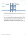
1
XBee
865/868 LP RF
Modules
Model: XBEE S8
Hardware: S8
Firmware: 8059
User Guide
Digi XBee 865/868 LP RF Modules User Guide
(Part number 90002126 K)
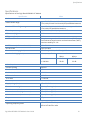
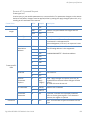
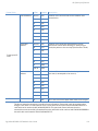
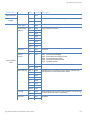
Revision
Date
Description
A
February, 2012
Baseline release of the document.
B
October, 2012
Changed the value of the XBee 865/868LP module from 40g to 5g in the
Specifications section.
C
April, 2013
Added a Channel Frequency table.
D
April, 2013
Made corrections to NB parameter; added HP and CM parameters; removed
“Internal Pin Mappings” from manual. Changed parameter values in NB
description from “0 to 4" to “0 to 2."
E
July, 2013
Removed Frame ID section for 0x90 frame/ 64 bit source address. Added
description of AT command %V under I/O Commands Reference Table.
Included details of restrictions on the Embedded PCB antenna under Antenna
Options and under XBee RF Module section. Updated the description of CM
command under MAC/PHY basics section. Restored missing information in
the Networking Methods section, the Indirect Messaging and Polling section,
and the Warranty sections.
F
October, 2013
Changed power supply voltage from 250mV to 50mV.
G
July, 2014
Changed frequencies values of channel 8, 9, 22 and 10 in the channel
frequencies table. Fixed the Parameter Range field of CM parameter.
H
October, 2014
Fixed reference to AG command in the Network link establishment and
maintenance section. Added the max network size message in the Digi XBee
865/868LP RF module hardware section.
I
Revision I is skipped.
J
November, 2014
Corrected Pin 7 typos on pages 15 and 129. Corrected the schematic on page
22.
K
March, 2015
Replaced the warranty section. Removed a duplicate description of the HP
command. Removed the DC and TA commands. Corrected other parameters.
Corrected the formula provided for transmitting a broadcast. Added transmit
options to the Explicit Addressing Command Frame. Created a
troubleshooting section. Added effective isotropic radiated power (e.i.r.p.)
notes.
Disclaimers
Information in this document is subject to change without notice and does not represent a commitment on
the part of Digi International. Digi provides this document “as is,” without warranty of any kind, expressed
or implied, including, but not limited to, the implied warranties of fitness or merchantability for a particular
purpose. Digi may make improvements and/or changes in this manual or in the product(s) and/or the
program(s) described in this manual at any time.
Trademarks and copyright
Digi, Digi International, and the Digi logo are trademarks or registered trademarks in the United States and
other countries worldwide. All other trademarks mentioned in this document are the property of their
respective owners.
© 2015 Digi International. All rights reserved.
Warranty
View the product’s warranty online: http://www.digi.com/howtobuy/terms
Customer support
Telephone (8:00 am — 5:00 pm CST):
US & Canada: 866.765.9885
Worldwide: 801.765.9885
Online: www.digi.com/support/eservice
Mail:
Digi International
11001 Bren Road East
Minnetonka, MN 55343
USA
Related documentation
For basic information to help get you started on the XBee-PRO 868 Modules, navigate to the Getting Started
Guide at www.digi.com/support.
Document number
Document name
90002155
XBee-PRO 868 Development Kit Getting Started Guide
Digi XBee 865/868 LP RF Modules User Guide
3
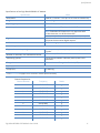
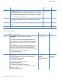
Contents
Module hardware 9
XBee S8 hardware description 9
European acceptance 9
Specifications 10
Serial communications specifications 12
UART serial connections 12
SPI serial connections 13
GPIO specifications 13
Hardware specifications for the programmable variant 13
Mechanical drawings 14
Pin signals 15
Design notes 16
Power supply design 16
Recommended pin connections 16
Board layout 17
Design notes for PCB antenna modules 17
Design notes for RF pad modules 19
Module operation for the Programmable variant 21
XBee bootloader for the Programmable variant 23
Overview 23
Bootloader software specifics 23
Bootloader menu commands 26
Firmware updates 27
Output file configuration 28
Digi XBee 865/868LP RF Module operation 29
Listen Before Talk + Automatic Frequency Agility (LBT+AFA): g band mode 30
g4 Band mode 30
Serial communications 30
UART data flow 31
Serial data 31
SPI communications 31
SPI operation 32
Implementation of SPI 32
SPI signals 32
Full duplex operation 33
Digi XBee 865/868 LP RF Modules User Guide
4
Low power operation 34
Configuration 34
Serial port selection 34
Data format 35
SPI parameters 35
Serial buffers 35
Serial receive buffer 35
Serial transmit buffer 35
UART flow control 36
CTS flow control 36
RTS flow control 36
Serial interface protocols 36
Transparent operation - UART 36
API operation 37
Transparent operation vs API operation 37
Modes of operation 38
Transmit Mode 38
Receive Mode 39
Command Mode 39
Entering AT Command Mode 39
Sending AT commands 40
Command response in the AT Command Mode 40
Applying command changes in the AT Command Mode 40
Sleep Mode 41
Troubleshooting 41
Forcing UART operation 41
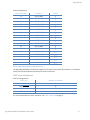
Digi XBee 865/868LP RF Module advanced application features 42
Remote configuration commands 42
Sending a remote command 42
Applying changes on remote devices 42
Remote command responses 42
Network commissioning and diagnostics 43
Device configuration 43
Network link establishment and maintenance 43
Building aggregate routes 43
Node replacement 44
Device placement 44
Link testing 44
RSSI indicators 44
Device discovery 45
Network discovery 45
Neighbor polling 45
Link reliability 45
Network link testing 45
Link testing between adjacent devices 46
Trace routing 47
NACK messages 48
Commissioning pushbutton and associate LED 48
Commissioning pushbutton 49
Associate LED 49
Diagnostics support 50
I/O Line monitoring 51
Digi XBee 865/868 LP RF Modules User Guide
5
I/O samples 51
Queried sampling 51
Periodic I/O sampling 53
Digital I/O change detection 53
General purpose flash memory 53
Accessing general purpose flash memory 53
Over-the-Air firmware upgrades 60
Distributing the new application 60
Verifying the new application 61
Installing the application 61
Things to remember 61
Digi XBee 865/868LP RF Module networking methods 62
Directed Broadcast/Repeater mode 62
Point to Point/Multipoint mode 62
Permanent (dedicated) 62
Switched 62
DigiMesh networking 62
DigiMesh feature set 63
Networking concepts 63
Device configuration 63
Network ID 63
Data transmission and routing 63
Unicast addressing 63
Broadcast addressing 63
Routing 64
Route discovery 64
Throughput 64
Transmission timeouts 65
Unicast one hop time 65
Transmitting a broadcast 65
Transmitting a unicast with a known route 66
Transmitting a unicast with an unknown route 66
Transmitting a unicast with a broken route 66
Digi XBee 865/868LP RF Modules sleep mode 67
Normal mode (SM=0) 67
Asynchronous pin sleep mode (SM=1) 67
Asynchronous cyclic sleep mode (SM=4) 68
Asynchronous cyclic sleep with pin wake up mode (SM=5) 68
Synchronous sleep support mode (SM=7) 68
Synchronous cyclic sleep mode (SM=8) 68
Asynchronous sleep operation 68
Wake timer 68
Indirect messaging and polling 69
Indirect messaging 69
Polling 69
Sleeping routers 69
Operation 70
Synchronization messages 70
Becoming a sleep coordinator 71
Configuration 73
Digi XBee 865/868 LP RF Modules User Guide
6
Diagnostics 76
Digi XBee 865/868LP RF Modules command reference tables 77
Special commands 77
MAC/PHY level commands 78
Diagnostics commands 79
Network commands 81
Addressing commands 82
Addressing discovery/configuration commands 84
Diagnostic addressing 86
Security commands 86
Serial Interfacing commands 86
I/O Settings commands 87
I/O Sampling commands 92
Sleep commands 93
Sleep diagnostics commands 95
AT command options 96
Firmware commands 96
Digi XBee 865/868LP RF Modules API operation 97
API frame specifications 97
API operation (AP parameter = 1) 97
API operation - with escape characters (AP parameter = 2) 97
Data bytes that need to be escaped: 98
Length 98
Frame data 98
Checksum 99
API UART exchanges 99
AT commands 99
Transmitting and receiving RF data 100
Remote AT commands 100
Supporting the API 100
Frame data 101
AT command 101
AT command - Queue parameter value 101
Transmit Request 102
Explicit Addressing Command Frame 104
Remote AT Command Request 106
AT Command Response 107
Modem Status 108
Transmit Status 108
Route Information Packet 109
Aggregate Addressing Update 111
Receive Packet 112
Explicit Rx Indicator 113
Node Identification Indicator 114
Remote Command Response 116
Digi XBee 865/868LP RF Modules agency certifications 118
Europe (ETSI) 118
OEM labeling requirements 118
Digi XBee 865/868 LP RF Modules User Guide
7
CE labeling requirements 118
Restrictions 119
Declarations of Conformity 119
Antenna 119
Migrating from XBee through-hole to XBee SMT modules 120
Pin mapping 120
Mounting the modules 121
Digi XBee 865/868LP RF Modules manufacturing information 123
Recommended solder reflow cycle 123
Recommended footprint 124
Flux and cleaning 125
Reworking 125
Digi XBee 865/868 LP RF Modules User Guide
8
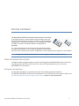
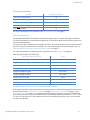
Module hardware
The Digi XBee 865/868LP RF Modules provide wireless connectivity
to end-point devices in mesh networks. With the XBee, users can
have their network up-and-running in a matter of minutes without
configuration or additional development. The Digi XBee 865/868LP
RF Module consists of firmware loaded onto Digi XBee S8
hardware.
You can build networks up to 128 nodes using the XBee modules.
For larger networks up to 1000+ nodes, Digi offers RF Optimization
Services to assist with proper network configuration. Contact Digi Technical Support for more details.
Note The Digi XBee 865/868LP RF Modules are not compatible with other XBee products.
XBee S8 hardware description
The XBee S8 radio module hardware consists of an Energy Micro EFM®32G230F128 microcontroller,
an Analog Devices ADF7023 radio transceiver, and in the Programmable version, a Freescale
MC9S08QE32 microcontroller.
European acceptance
The Digi XBee 865/868LP is manufactured under ISO 900:2000 registered standards.
The Digi XBee 865/868LP RF Modules are optimized for use in Europe and other regions. Refer to the
Digi XBee 865/868LP RF Modules agency certifications section for more information.
Digi XBee 865/868 LP RF Modules User Guide
9
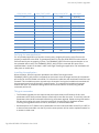
Specifications
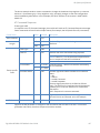
Specifications
Specifications of the Digi XBee 865/868LP RF Module
Specification
XBee
Performance
Indoor/urban range1
Up to 500 ft (150 m) with 2.1 dBi antenna, up to 250 ft
(75 m) with printed circuit board (PCB) embedded antenna.
Outdoor RF line-of-sight range1
Up to 2.5 miles (4 km) with 2.1 dBi antenna, up to 0.6 miles
(1 km) with PCB embedded antenna.
Transmit power output
Up to 14 dBm (25 mW) e.i.r.p. with 2 dBi antenna
RF data rate (high)
80 kb/s
RF data rate (low)
10 kb/s
UART interface
Complementary metal–oxide–semiconductor (CMOS)
Serial universal asynchronous receiver/transmitter (UART),
baud rate stability of <1%.
UART data rate (software selectable)
9600-230400 baud
SPI clock rate
Up to 3.5 MHZ
Receiver sensitivity (typical)
-101 dBm @ 80 kb/s, -106 dBm @ 10 kb/s.
Receiver blocking (typical)
Frequency offset
Data rate
10kb/s
80kb/s
+/- 400 kHz
40 dB
35 dB
+/- 200 kHz
35 dB
29 dB
LBT+AFA performance
Channel spacing
100 kHz
Receiver bandwidth
150 kHz
Modulation bandwidth
< 300 kHz
LBT threshold
< -88 dBm
TX on time
< 1 second
Power requirements
Supply voltage (VDD)
2.7 to 3.6 VDC
Transmit current, high data rate
48 mA, (45 mA typical)
Transmit current, low data rate
47 mA (41 mA typical)
Idle / receive current (high data rate)
27 mA (22 mA typical)
Idle / receive current (low data rate)
26 mA (24 mA typical)
Sleep current
1.7 μA
General
Operating frequency band2
863 to 870 MHZ for Europe.
865 to 867 MHZ for India.
Digi XBee 865/868 LP RF Modules User Guide
10
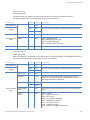
Specifications
Specifications of the Digi XBee 865/868LP RF Module
Specification
XBee
Dimensions
0.866 in x 1.333 in x 1.2 in (2.119 cm x 3.4 cm x 0.305 cm)
Weight
1.4 oz. (40 g)
Operating temperature
-40º to 85º C (industrial)
Antenna options
U. FL RF connector, RF pad, embedded PCB antenna.
Note Embedded PCB antenna is only approved with
10 kb/s data rate, not 80 kb/s data rate.
Digital I/O
13 I/O lines, five dedicated to Serial Peripheral Interface
(SPI) that can be used as digital outputs.
ADC
4 10-bit analog inputs
Networking and security
Supported network topologies
Mesh, repeater, point-to-point, point-to-multipoint, peerto-peer.
Number of channels, user selectable channels2
30 channels, LBT + AFA
Addressing options
Personal Area Network identifier (PAN ID) and 64-bit
addresses.
Encryption
128 bit Advanced Encryption Standard (AES)
Agency approvals
CE Marking
Europe (CE) 2
1. To determine your range, perform a range test under your operating conditions.
2. See Restrictions on page 119 for countries in the European Community.
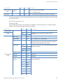
Channel frequencies
Channel Number
Frequency
Bands
0
863.15 MHZ
g
1
863.35 MHZ
g
2
863.55 MHZ
g
3
863.75 MHZ
g
4
863.95 MHZ
g
5
864.15 MHZ
g
6
864.35 MHZ
g
7
864.55 MHZ
g
8
864.75 MHZ
g
9
864.95 MHZ
g
10
865.15 MHZ
g
11
865.35 MHZ
g
Digi XBee 865/868 LP RF Modules User Guide
11
Specifications
Channel frequencies
Channel Number
Frequency
Bands
12
865.55 MHZ
g
13
865.75 MHZ
g
14
865.95 MHZ
g
15
866.15 MHZ
g
16
866.35 MHZ
g
17
866.55 MHZ
g
18
866.75 MHZ
g
19
866.95 MHZ
g
20
867.15 MHZ
g
21
867.35 MHZ
g
22
867.55 MHZ
g
23
867.75 MHZ
g
24
867.95 MHZ
g
25
868.15 MHZ
g, g1
26
868.35 MHZ
g, g1
27
868.85 MHZ
g, g2
28
869.05 MHZ
g, g2
29
869.85 MHZ
g, g4
Serial communications specifications
The Digi XBee 865/868LP RF Modules support both Universal Asynchronous Receiver / Transmitter
(UART) and Serial Peripheral Interface (SPI) serial connections.
UART serial connections
UART pin assignments
UART Pins
Module Pin Number
DOUT
3
DIN / CONFIG
4
CTS / DIO7
25
RTS / DIO6
29
For more information on UART operation, see UART data flow on page 31.
Digi XBee 865/868 LP RF Modules User Guide
12
Specifications
SPI serial connections
SPI Pins
Module Pin Number
SPI_SCLK / DIO18 (input)
14
SPI_SSEL / DIO17 (input)
15
SPI_MOSI / DIO16 (input)
16
SPI_MISO / DIO15 (output/tri-stated)
17
SPI_ATTN (output)
12
For more information on SPI operation, see SPI communications on page 31.
GPIO specifications
The Digi XBee 865/868LP RF Modules have General Purpose Input / Output (GPIO) ports available.
The exact list depends on the module configuration, as some GPIO pads are used for purposes such
as serial communication.
You can set the pin configuration by using D0-D9, P0-P9, and I/O line monitoring. You cannot sample
pins P5-P9, but you may use them as outputs. For more information on these commands, see Digi
XBee 865/868LP RF Modules command reference tables on page 77.
For more information on configuring and using GPIO ports, see Pin signals on page 15.
Electrical specifications for GPIO pads
GPIO Electrical Specification
Value
Low Schmitt switching threshold
0.3 x VDD
High Schmitt switching threshold
0.7 x VDD
Input pull-up resistor value
40 k
Input pull-down resistor value
40 k
Output voltage for logic 0
0.05 x VDD
Output voltage for logic 1
0.95 x VDD
Output source current
6 mA
Output sink current
6 mA
Total output current (for GPIO pads)
48 mA
Hardware specifications for the programmable variant
If the module includes the programmable secondary processor, add the following table values to the
specifications listed in UART pin assignments on page 12, SPI serial connections on page 13, and
GPIO specifications on page 13. For example, if the secondary processor is running at 20 MHZ and
the primary processor is in receive mode, then the new current value will be Itotal = Ir2 + Irx = 14 mA
+ 9 mA = 23 mA, where Ir2 is the runtime current of the secondary processor and Irx is the receive
current of the primary.
Digi XBee 865/868 LP RF Modules User Guide
13
Specifications
Specifications of the programmable secondary processor
Optional secondary processor specification
Add these numbers to specifications1
Runtime current for 32k running at 20MHZ
+14 mA
Runtime current for 32k running at 1MHZ
+1 mA
Sleep current
+0.5 A typical
VREF Range
1.8 VDC to VDD
Microcontroller
Freescale Flexis 8-bit S08 microcontroller
Freescale S08QE Family
Part number: MC9S08QE32
1. Add to RX, TX, and sleep currents depending on the mode of operation.
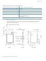
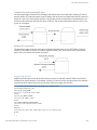
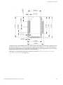
Mechanical drawings
The following figures shows the mechanical drawings of the Digi XBee 865/868LP RF Modules.
Antenna options are not shown.
Note All dimensions are in inches.
Digi XBee 865/868 LP RF Modules User Guide
14
Specifications
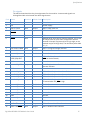
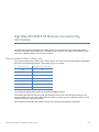
Pin signals
The table belows describes the pin assignments for the modules. Low-asserted signals are
distinguished with a horizontal line above signal name.
Pin # Name
Direction
Default State Description
1
GND
-
-
Ground
2
VDD
-
-
Power Supply
3
DIO13 / DOUT
Both
Output
GPIO / UART Data Out
4
DIO14 / DIN /
CONFIG
Both
Input
GPIO / UART Data In
5
DIO12
Both
GPIO
6
RESET
Both
Module Reset. Drive low to reset the module. This is also
an output with an open drain configuration with an
internal 20 k pull-up (never drive to logic high, as the
module may be driving it low). The minimum pulse width
is 1 S.
7
DIO10/RSSI PWM0
Both
Output
GPIO / RX Signal Strength Indicator
8
DIO11 / PWM1
Both
Disabled
GPIO / Pulse Width Modulator
9
[reserved]
-
Disabled
Do Not Connect
10
DIO8 /
SLEEP_REQUEST
Both
Input
GPIO / Pin Sleep Control Line
11
GND
-
-
Ground
12
DIO19 / SPI_ATTN
Output
Output
Serial Peripheral Interface Attention or UART Data
Present indicator
13
GND
-
-
Ground
14
DIO18 / SPI_CLK
Input
Input
GPIO / Serial Peripheral Interface Clock
15
DIO17 / SPI_SSEL
Input
Input
GPIO / Serial Peripheral Interface not Select
16
DIO16 / SPI_MOSI
Input
Input
GPIO / Serial Peripheral Interface Data In
17
DIO15 / SPI_MISO
Output
Output
GPIO / Serial Peripheral Interface Data Out
Tri-stated when SPI_SSEL is high
18
[reserved]*
-
Disabled
Do Not Connect
19
[reserved]*
-
Disabled
Do Not Connect
20
[reserved]*
-
Disabled
Do Not Connect
21
[reserved]*
-
Disabled
Do Not Connect
22
GND
-
-
Ground
23
[reserved]
-
Disabled
Do Not Connect
24
DIO4
Both
Disabled
GPIO
25
DIO7 / CTS
Both
Output
GPIO / Clear to Send Flow Control
26
DIO9 / ON/SLEEP
Both
Output
GPIO / Module Status Indicator
(DTR on the dev board)
Digi XBee 865/868 LP RF Modules User Guide
15
Specifications
Pin # Name
Direction
Default State Description
27
VREF
Input
-
Not used internally, used for programmable secondary
processor. For compatibility with other XBee modules,
we recommend connecting this pin to the voltage
reference if Analog Sampling is desired. Otherwise,
connect to GND.
28
DIO5 / ASSOCIATE
Both
Output
GPIO / Associate Indicator
29
DIO6 / RTS
Both
Input
GPIO / Request to Send Flow Control
30
DIO3 / AD3
Both
Disabled
GPIO / Analog Input
31
DIO2 / AD2
Both
Disabled
GPIO / Analog Input
32
DIO1 / AD1
Both
Disabled
GPIO / Analog Input
33
DIO0 / AD0
Both
Input
GPIO / Analog Input
34
[reserved]
-
Disabled
Do Not Connect
35
GND
-
-
Ground
36
RF
Both
-
RF I/O for RF Pad Variant
37
[reserved]
-
Disabled
Do Not Connect
2. Signal Direction is specified with respect to the module.
3. See the Design notes section below for details on pin connections.
4. * These pins are not available for customer use.
Design notes
The Digi XBee 865/868LP RF Modules do not specifically require any external circuitry or specific
connections for proper operation. However, there are some general design guidelines that are
recommended for help in troubleshooting and building a robust design.
Power supply design
Poor power supply can lead to poor radio performance, especially if the supply voltage is not kept
within tolerance or is excessively noisy. To help reduce noise, we recommend placing both a 1F and
47 pF capacitor as near to pin 2 on the PCB as possible. If you are using a switching regulator for your
power supply, switching frequencies above 500 kHz are preferred. Power supply ripple should be
limited to a maximum 250 mV peak to peak.
Note For designs using the programmable modules, an additional 10 F decoupling cap is
recommended near pin 2 of the module. The nearest proximity to pin 2 of the three caps
should be in the following order: 47 pf, 1 F followed by 10 F.
Recommended pin connections
The only required pin connections are VDD, GND, DOUT and DIN. Connect VDD, GND, DOUT, DIN, RTS,
and DTR to support serial firmware updates.
Leave all unused pins disconnected. Use the PR and PD software commands to pull all of the inputs
on the radio high or low with 40k internal pull-up or pull-down resistors. No specific treatment is
needed for unused outputs.
Digi XBee 865/868 LP RF Modules User Guide
16
Specifications
For applications that need to ensure the lowest sleep current, never leave unconnected inputs
floating. Use internal or external pull-up or pull-down resistors, or set the unused I/O lines to
outputs.
Other pins may be connected to external circuitry for convenience of operation, including the
Associate LED pad (pad 28) and the Commissioning pad (pad 33). The Associate LED pad flashes
differently depending on the state of the module to the network, and a pushbutton attached to pad
33 can enable various join functions without having to send serial port commands. For more details,
see Commissioning pushbutton and associate LED on page 48. The source and sink capabilities are
limited to 6 mA on all I/O pads.
The VRef pad (pad 27) is only used on the programmable versions of these modules. For
compatibility with other XBee modules, we recommend connecting this pin to a voltage reference if
analog sampling is desired. Otherwise, connect it to GND.
Board layout
Digi XBee 865/868LP RF Modules are designed to be self sufficient and have minimal sensitivity to
nearby processors, crystals or other PCB components. As with all PCB designs, Power and Ground
traces should be thicker than signal traces and able to comfortably support the maximum current
specifications. A recommended PCB footprint for the module is available in Digi XBee 865/868LP RF
Modules manufacturing information on page 123. Aside from antenna selection, no other special
PCB design considerations are required for integrating XBee radios.
The choice of antenna and antenna location is very important for optimal performance. With the
exception of the RF Pad variant, Digi XBee 865/868LP RF Modules do not require additional ground
planes on the host PCB. In general, antenna elements radiate perpendicular to the direction they
point. Thus a vertical antenna emits across the horizon. Metal objects near the antenna cause
reflections and may reduce the ability for an antenna to radiate efficiently. Metal objects between the
transmitter and receiver can also block the radiation path or reduce the transmission distance, so
external antennas should be positioned away from them as much as possible. Some objects that are
often overlooked are metal poles, metal studs or beams in structures, concrete (it is usually
reinforced with metal rods), metal enclosures, vehicles, elevators, ventilation ducts, refrigerators,
microwave ovens, batteries, and tall electrolytic capacitors.
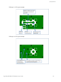
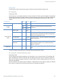
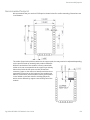
Design notes for PCB antenna modules
PCB Antenna modules should not have any ground planes or metal objects above or below the
antenna. For best results, do not place the module in a metal enclosure, which may greatly reduce
the range. Place the module at the edge of the PCB on which it is mounted. The ground, power and
signal planes should be vacant immediately below the antenna section. The drawing on the following
page illustrates important recommendations for designing with the PCB Antenna module. For
optimal performance, do not mount this module on the RF Pad footprint described in the next
section because the footprint requires a ground plane within the PCB Antenna keep out area.
Digi XBee 865/868 LP RF Modules User Guide
17
Specifications
XBee/ XBee-PRO SMT
PCB Antenna
Keepout Area
Digi XBee 865/868 LP RF Modules User Guide
18
Specifications
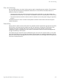
Design notes for RF pad modules
The RF Pad is a soldered antenna connection. The RF signal travels from pin 36 on the module to the
antenna through an RF trace transmission line on the PCB. Any additional components between the
module and antenna will violate modular certification. The RF trace should have a controlled
impedance of 50 . We recommend using a microstrip trace, although you may also use coplanar
waveguide if more isolation is needed. Microstrip generally requires less area on the PCB than
coplanar waveguide. We do not recommend Stripline because sending the signal to different PCB
layers can introduce matching and performance problems.
It is essential to follow good design practices when implementing the RF trace on a PCB. Consider the
following points:
•
The following figures show a layout example of a host PCB that connects an RF Pad module to a
right angle, through-hole RPSMA jack.
•
The top two layers of the PCB have a controlled thickness dielectric material in between them.
•
The second layer has a ground plane that runs underneath the entire RF Pad area. This ground
plane is a distance d, the thickness of the dielectric, below the top layer.
•
The top layer has an RF trace running from pin 36 of the module to the RF pin of the RPSMA
connector.
•
The RF trace's width determines the impedance of the transmission line with relation to the
ground plane.
•
Many online tools can estimate this value, but you should consult the PCB manufacturer for the
exact width.
•
Assuming d=0.025”, and that the dielectric has a relative permittivity of 4.4, the width in this
example will be approximately 0.045" for a 50 trace. This trace width is a good fit with the
module footprint's 0.060" pad width.
•
We do not recommend using a trace wider than the pad width, and using a very narrow trace
(under 0.010") can cause unwanted RF loss.
•
The length of the trace is minimized by placing the RPSMA jack close to the module.
•
All of the grounds on the jack and the module are connected to the ground planes directly or
through closely placed vias.
•
Space any ground fill on the top layer at least twice the distance d (in this case, at least 0.050")
from the microstrip to minimize their interaction.
Implementing these design suggestions ensures that the RF Pad module performs to its
specifications.
Digi XBee 865/868 LP RF Modules User Guide
19
Specifications
PCB Layer 1 of RF layout example
PCB Layer 2 of RF layout example
Digi XBee 865/868 LP RF Modules User Guide
20
Specifications
Module operation for the Programmable variant
The modules with the programmable option have a secondary processor with 32k of flash and 2k of
random-access memory (RAM). This allows module integrators to put custom code on the XBee
module to fit their own unique needs. The DIN, DOUT, RTS, CTS, and RESET lines are intercepted by
the secondary processor to allow it to be in control of the data transmitted and received. All other
lines are in parallel and can be controlled by either the internal microcontroller or the MC9S08QE
micro; see the block diagram under Digi XBee 865/868LP RF Module operation on page 29 for details.
The internal microcontroller has control of certain lines by default. The internal microcontroller can
release these lines by sending the proper command(s) to disable the desired DIO line(s). For more
information, see Digi XBee 865/868LP RF Modules command reference tables on page 77.
In order for the secondary processor to sample with ADCs, you must connect the XBee pin 27 (VREF)
to a reference voltage.
Digi provides a bootloader that can take care of programming the processor over the air or through
the serial interface. This means that over the air updates can be supported through an XMODEM
protocol. The processor can also be programmed and debugged through a one wire interface BKGD
(Pin 9).
Digi XBee 865/868 LP RF Modules User Guide
21
Specifications
Digi XBee 865/868 LP RF Modules User Guide
22
Specifications
XBee bootloader for the Programmable variant
Overview
The Digi XBee 865/868LP RF Programmable variant includes a Freescale MC9S08QE32 application
processor. This application processor comes with a bootloader. This section describes how to
interface your application code running on this processor using the XBee Programmable module's
bootloader.
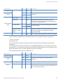
Bootloader software specifics
Memory layout
The image on the right shows the memory
map for the MC9S08QE32 application
processor. The supplied bootloader
occupies the bottom pages of the flash
from 0xF200 to 0xFFFF. Application code
cannot write to this space.
The application code can exist in Flash
from address 0x8400 to 0xF1BC. 1k of
Flash from 0x8000 to 0x83FF is reserved
for Non Volatile Application Data that is
not be erased by the bootloader during a
flash update.
A portion of RAM is accessible by both the
application and the bootloader.
Specifically, there is a shared data region
used by both the application and the
bootloader that is located at RAM address
0x200 to 0x215. Application code should
not write anything to BLResetCause or
AppResetCause unless informing the
bootloader of the impending reset reason.
The Application code should not clear
BLResetCause unless it is handling the
unexpected reset reason.
To prevent a malfunctioning application
from running forever, the Bootloader
increments BLResetCause after each
watchdog or illegal instruction reset. If this
register reaches above 0x10 the
bootloader will stop running the
application for a few minutes to allow an
OTA or Local update to occur. If no update
is initiated within the time period,
BLResetCause is cleared and the
application is started again. To prevent
unexpected halting of the application, the
application shall clear or decrement
BLResetCause just before a pending reset.
To disable this feature, the application
clears BLResetCause at the start of the application.
Digi XBee 865/868 LP RF Modules User Guide
23
Specifications
Operation
Upon reset of any kind, the execution control begins with the bootloader.
If the reset cause is Power-On reset (POR), Pin reset (PIN), or Low Voltage Detect (LVD) reset (LVD) the
bootloader will not jump to the application code if the override bits are set to RTS(D7)=1, DTR(D5)=0,
and DIN(B0)=0. Otherwise, the bootloader writes the reset cause NOTHING to the shared data region,
and jumps to the Application.
Reset causes are defined in the file common. h in an enumeration with the following definitions:
typedef enum {
BL_CAUSE_NOTHING
= 0x0000, //PIN, LVD, POR
BL_CAUSE_NOTHING_COUNT
= 0x0001,//BL_Reset_Cause counter
// Bootloader increments cause every reset
BL_CAUSE_BAD_APP
= 0x0010,//Bootloader considers APP invalid
} BL_RESET_CAUSES;
typedef enum {
APP_CAUSE_NOTHING
= 0x0000,
APP_CAUSE_USE001
= 0x0001,
// 0x0000 to 0x00FF are considered valid for APP use.
APP_CAUSE_USE255
= 0x00FF,
APP_CAUSE_FIRMWARE_UPDATE = 0x5981,
APP_CAUSE_BYPASS_MODE
= 0x4682,
APP_CAUSE_BOOTLOADER_MENU = 0x6A18,
} APP_RESET_CAUSES;
Otherwise, if the reset cause is a watchdog or other reset, the bootloader checks the shared memory
region for the APP_RESET_CAUSE. If the reset cause is:
1. APP_CAUSE_NOTHING or 0x0000 to 0x00FF, the bootloader increments the BL_RESET_CAUSES,
verifies that it is still less than BL_CAUSE_BAD_APP, and jumps back to the application. If the
Application does not clear the BL_RESET_CAUSE, it can prevent an infinite loop of running a bad
application that continues to perform illegal instructions or watchdog resets.
2. APP_CAUSE_FIRMWARE_UPDATE, the bootloader has been instructed to update the application
over-the-air from a specific 64-bit address.In this case, the bootloader will attempt to initiate an
Xmodem transfer from the 64-bit address located in shared RAM.
3. APP_CAUSE_BYPASS_MODE, the bootloader executes bypass mode. This mode passes the local
UART data directly to the internal microcontroller allowing for direct communication with the
internal microcontroller. The only way to exit bypass mode is to reset or power cycle the module.
If none of the above is true, the bootloader will enter Command mode. In this mode, users can
initiate firmware downloads both wired and over-the-air, check application/bootloader version
strings, and enter Bypass mode.
Application version string
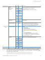
The figure above shows an Application version string pointer area in application flash which holds
the pointer to where the application version string resides. The application's linker command file
ultimately determines where this string is placed in application flash.
It is preferable that the application version string be located at address 0x8400 for MC9S08QE32
parts. The application string can be any characters terminated by the NULL character (0x00).There is
not a strict limit on the number of characters in the string, but for practical purposes should be kept
under 100 bytes including the terminating NULL character. During an update the bootloader erases
the entire application from 0x8400 on. The last page has the vector table specifically the redirected
Digi XBee 865/868 LP RF Modules User Guide
24
Specifications
reset vector. The version string pointer and reset vector are used to determine if the application is
valid.
Application Interrupt Vector table and Linker command file
Since the bootloader flash region is read-only, the interrupt vector table is redirected to the region
0xF1C0 to 0xF1FD so that application developers can use hardware interrupts. Note that in order for
Application interrupts to function properly, the Application's linker command file (*.prm extension)
must be modified appropriately to allow the linker to place the developers code in the correct place
in memory. For example, the developer desires to use the serial communications port SCI1 receive
interrupt. The developer would add the following line to the Codewarrior linker command file for the
project:
VECTOR ADDRESS 0x0000F1E0 vSci1Rx
This will inform the linker that the interrupt function vSci1Rx() should be placed at address
0x0000F1E0. Next, the developer should add a file to their project vector_table.c that creates an array
of function pointers to the ISR routines used by the application.
extern void _Startup(void);/* _Startup located in Start08.c */
extern void vSci1Rx(void);/* sci1 rx isr */
extern short iWriteToSci1(unsigned char *);
void vDummyIsr(void);
#pragma CONST_SEG VECTORS
void (* const vector_table[])(void) = /* Relocated Interrupt vector table */{
vDummyIsr,/* Int.no. 0 Vtpm3ovf (at F1C0)Unassigned */
vDummyIsr, /* Int.no. 1 Vtpm3ch5 (at F1C2)
Unassigned */
vDummyIsr, /* Int.no. 2 Vtpm3ch4 (at F1C4)
Unassigned */
vDummyIsr, /* Int.no. 3 Vtpm3ch3 (at F1C6)
Unassigned */
vDummyIsr, /* Int.no. 4 Vtpm3ch2 (at F1C8)
Unassigned */
vDummyIsr, /* Int.no. 5 Vtpm3ch1 (at F1CA)
Unassigned */
vDummyIsr, /* Int.no. 6 Vtpm3ch0 (at F1CC)
Unassigned */
vDummyIsr, /* Int.no. 7 RTCs (at F1CE)
Unassigned */
vDummyIsr, /* Int.no. 8 Vsci2tx (at F1D0)
Unassigned */
vDummyIsr, /* Int.no. 9 Vsci2rx (at F1D2)
Unassigned */
vDummyIsr, /* Int.no. 10 Vsci2err (at F1D4)
Unassigned */
vDummyIsr, /* Int.no. 11 Vacmpx (at F1D6)
Unassigned */
vDummyIsr, /* Int.no. 12 Vadc (at F1D8)
Unassigned */
vDummyIsr, /* Int.no. 13 Vkeyboard (at F1DA)
Unassigned */
vDummyIsr, /* Int.no. 14 Viic (at F1DC)
Unassigned */
vDummyIsr, /* Int.no. 15 Vsci1tx (at F1DE)
Unassigned */
vSci1Rx,
/* Int.no. 16 Vsci1rx (at F1E0)
SCI1RX */
vDummyIsr, /* Int.no. 17 Vsci1err (at F1E2)
Unassigned */
vDummyIsr, /* Int.no. 18 Vspi (at F1E4)
Unassigned */
vDummyIsr, /* Int.no. 19 VReserved12 (at F1E6) Unassigned */
vDummyIsr, /* Int.no. 20 Vtpm2ovf (at F1E8)
Unassigned */
vDummyIsr, /* Int.no. 21 Vtpm2ch2 (at F1EA)
Unassigned */
vDummyIsr, /* Int.no. 22 Vtpm2ch1 (at F1EC)
Unassigned */
vDummyIsr, /* Int.no. 23 Vtpm2ch0 (at F1EE)
Unassigned */
vDummyIsr, /* Int.no. 24 Vtpm1ovf (at F1F0)
Unassigned */
vDummyIsr, /* Int.no. 25 Vtpm1ch2 (at F1F2)
Unassigned */
vDummyIsr, /* Int.no. 26 Vtpm1ch1 (at F1F4)
Unassigned */
vDummyIsr, /* Int.no. 27 Vtpm1ch0 (at F1F6)
Unassigned */
vDummyIsr, /* Int.no. 28 Vlvd (at F1F8)
Unassigned */
vDummyIsr, /* Int.no. 29 Virq (at F1FA)
Unassigned */
vDummyIsr, /* Int.no. 30 Vswi (at F1FC)
Unassigned */
Digi XBee 865/868 LP RF Modules User Guide
25
Specifications
_Startup
/* Int.no. 31 Vreset (at F1FE)
};
void vDummyIsr(void){
for(;;){
if(iWriteToSci1("STUCK IN UNASSIGNED ISR\n\r>"));
}
}
Reset vector */
The interrupt routines themselves can be defined in separate files. The vDummyIsr function is used in
conjunction with iWritetoSci1 for debugging purposes.
Bootloader menu commands
The bootloader accepts commands from both the local UART and OTA. All OTA commands sent must
be Unicast with only 1 byte in the payload for each command. A response will be returned to the
sender. All Broadcast and multiple byte OTA packets are dropped to help prevent general OTA traffic
from being interpreted as a command to the bootloader while in the menu.
Bypass mode - B
The bootloader provides a bypass mode of operation that essentially connects the Freescale MCU to
the internal microcontroller’s serial UART. This allows direct communication to the internal
microcontroller’s radio for the purpose of firmware and radio configuration changes. Once in bypass
mode, the XCTU utility can change modem configuration and/or update module’s firmware. Bypass
mode automatically handles any baud rate up to 115.2 kb/s. This command is unavailable when the
module is accessed remotely.
Update firmware - F
The F command initiates a firmware download for both wired and over-the-air configurations.
Depending on the source of the command (received via Over the Air or local UART), the download will
proceed via wired or over-the-air respectively.
Adjust timeout for update firmware - T
The T command changes the timeout before sending a NAK by Base-Time*2^(T). The Base-Time for
the local UART is different than the Base-Time for Over the Air. During a firmware update, the
bootloader will automatically increase the Timeout if repeat packets are received or multiple NAKs
for the same packet without success occur.
Application version string - A
The A command provides the version of the currently loaded application. If no application is present,
Unknown will be returned.
Bootloader version string - V
The V command provides the version of the currently loaded bootloader. The version will return a
string in the format BLFFF-HHH-XYZ_DDD where FFF represents the Flash size in kilo bytes, HHH is the
hardware, XYZ is the version, and DDD is the preferred XMODEM packet size for updates. Double the
preferred packet size is also possible, but not guaranteed. For example BL032-2B0-023_064 will take
64 byte CRC XMODEM payloads and may take 128 byte CRC XMODEM payloads also. In this case,
both 64 and 128 payloads are handled, but the 64 byte payload is preferred for better Over the Air
reliability.
Bootloader Version BL032-2x0-025_064 only operates at 9600 baud on the local UART as well as
communications to the internal microcontroller. A newer version of the Bootloader BL032-2x0033_064 or newer BL032-2B0-XXX_064 has changed the baud rate to 115200 between the
Digi XBee 865/868 LP RF Modules User Guide
26
Specifications
Programmable and the internal microcontroller. The internal module is also set to 115200 as the
default baud rate. The default rate of the programmable local UART is also set to 115200, however,
the local UART has an auto baud feature added to detect if the UART is at the wrong baud rate. If a
single character is sent, it will automatically switch to 115200 or 9600 baud.
Firmware updates
Wired updates
You can update your application using the bootloader in a wired configuration with the following
steps:
1. Plug the XBee programmable module into a suitable serial port on a PC.
2. Open a hyperterminal (or similar dumb terminal application) session with 115200 baud, no parity,
and 8 data bits with one stop bit.
3. Press Enter to display the bootloader menu.
4. Press the F key to initiate a wired firmware update.
5. A series of C characters displays within the hyperterminal window. At this point, select the
transfer->send file menu item. Select the desired flat binary output file.
6. Select Xmodem as the protocol.
7. Click Send on the Send File dialog. The file downloads to the XBee Programmable module. Upon a
successful update, the bootloader jumps to the newly loaded application.
Over-The-Air updates
You can update your application using the bootloader in an over-the-air configuration with the
following steps.
Note This procedure assumes that the bootloader is running and not the application. The internal
microcontroller baud rate of the programmable module must be set to 115200 baud. The
bootloader only operates at 115200 baud between the Radio and programmable bootloader.
The application must be programmed with some way to support returning to the bootloader
in order to support Over the Air (OTA) updates without local intervention.
1. Open a hyperterminal session to the host module with no parity, no hardware flow control, 8 data
bits and 1 stop bit. (The host module does not have to operate at the same baud rate as the
remote module.) For faster updates and less latency due to the UART, set the host module to a
faster baud rate. (for example, 115200).
2. Type three pluses +++ to place the module in command mode (or XCTU’s Modem Configuration
tab can be used to set the correct parameters).
3. Set the Host Module destination address to the target module’s 64 bit address that the host
module will update (ATDH aabbccdd, ATDL eeffgghh, ATCN, where aabbccddeeffgghh is the
hexadecimal 64 bit address of the target module).
4. Press Enter and the bootloader command menu displays from the remote module.
5. Press the F key to cause the remote module to request the new firmware file over-the-air.
6. The host module begins receiving C characters indicating that the remote module is requesting an
Xmodem CRC transfer. Using XCTU or another terminal program, select XMODEM file transfer. Select
Digi XBee 865/868 LP RF Modules User Guide
27
Specifications
the Binary file to upload/transfer. Click Send to start the transfer. At the conclusion of a successful
transfer, the bootloader jumps to the newly loaded application.
Output file configuration
BKGD programming
P&E Micro provides a background debug tool that allows flashing applications on the MC9S08QE
parts through their background debug mode port. By default, the Codewarrior tool produces an ABS
output file for use in programming parts through the background debug interface. The
programmable XBee from the factory has the BKGD debugging capability disabled. In order to debug,
a bootloader with the debug interface enabled needs to be loaded on the secondary processor or a
stand-alone app needs to be loaded.
Bootloader updates
The supplied bootloader requires files in a flat binary format which differs from the default ABS file
produced. The Codewarrior tool also produces a S19 output file. In order to successfully flash new
applications, the S19 file must be converted into the flat binary format. Utilities are available on the
Internet that will convert S19 output to BIN outputs. In many cases, the BIN file conversion will pad the
addresses from 0x0000 to the code space with the same number (Often 0x00 or 0xFF). These extra
bytes before the APP code starts will need to be deleted from the bin file before the file can be
transferred to the bootloader.
Digi XBee 865/868 LP RF Modules User Guide
28
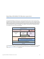
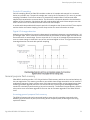
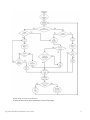
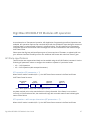
Digi XBee 865/868LP RF Module operation
The Digi XBee 865/868LP RF Module uses a multi-layered firmware base to order the flow of data,
dependent on the hardware and software configuration chosen by the user. This configuration block
diagram is shown below, with the host serial interface as the physical starting point, and the antenna
as the physical endpoint for the transferred data. As long as a block is able to touch another block,
the two interfaces can interact. For example, if the module is using SPI mode, Transparent mode is
not available as shown in the following image:
Host Serial Interface
UART
Transparent
Mode
SPI
AT Command
Mode
API
Mode
Command Handler
Packet Handler
Network Layer (DigiMesh/Repeater)
MAC/PHY Layer (Point-Multipoint)
Antenna
The command handler is the code that processes commands from AT Command Mode or API Mode;
see AT commands on page 99. The command handler can also process commands from remote
radios; see Remote AT commands on page 100.
Digi XBee 865/868 LP RF Modules User Guide
29
Listen Before Talk + Automatic Frequency Agility (LBT+AFA): g band mode
Listen Before Talk + Automatic Frequency Agility (LBT+AFA): g band mode
This radio implements Listen Before Talk (LBT) and Automatic Frequency Agility (AFA). The advantage
of LBT+AFA is that the radio can bypass the Duty Cycle requirement imposed by ETSI. LBT+AFA
requires that at least two frequencies be used for transmission. The g band mode contains several
sub-bands. See Module hardware on page 9 for a full list of channels and frequencies.
The advantage of this feature is that it gives a level of fairness to the radios in a given area. Before
this radio transmits, it senses a channel to determine if there is activity by taking an RSSI
measurement for 5 ms. If the measurement is below the threshold, then the radio transmits on that
channel. If there is activity, then that channel is not used, and the radio listens for at least 5ms to
allow transmissions to be received.
After the radio transmits on a channel, it will not transmit on that channel again until the minimum
TX off time has been met, which is greater than 100 ms. For this reason it is useful to have many
channels, so transmissions are not delayed.
There is also an ETSI requirement that only 100 seconds of transmission may occur over the period
of an hour on 200kHz of spectrum. This method simplifies and optimizes the calculations of
spectrum use over the period of one hour. As the ETSI specification states, the more channels you
have, the more transmission time you have in a one hour period. The effective duty cycle can be
calculated based on the number of available channels enabled as follows: Effective Duty Cycle =
(number of channels * 100) / 3600.
For example, if you enabled two channels you would have an effective duty cycle of 5.6%.
The XBee radio uses a sliding bucket algorithm to calculate usage over the period of 1 hour for each
channel. Each bucket accumulates for 6 minutes.
This radio has a maximum of 30 AFA channels that it can choose from, and channels can be excluded
by setting the channel mask (CM) to reduce them. Since not all countries allow for all of these
channels, the set may be dramatically smaller for some countries. For a complete list, refer to
www.digi.com.
g4 Band mode
When the channel mask is set to 0x20000000, the radio will be in g4 band mode. In this mode:
•
LBT+AFA mode is disabled
•
Module assumes no duty cycle requirement (or 100% duty cycle)
•
The PL setting must be set to 5 mW to comply with g4 band regulations.
Serial communications
RF Modules interface to a host device through a serial port. Through its serial port, the module can
communicate with any logic and voltage compatible UART, through a level translator to any serial
device (for example, through a RS-232 or USB interface board), or through an SPI, which is a
synchronous interface described in SPI parameters on page 35.
Digi XBee 865/868 LP RF Modules User Guide
30
Serial communications
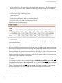
UART data flow
Devices that have a UART interface can connect directly to the pins of the RF module as shown in the
figure below.
System Data Flow Diagram in a UART-interfaced environment (Low-asserted signals distinguished with
horizontal line over signal name.
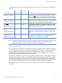
Serial data
Data enters the module UART through the DIN (pin 4) as an asynchronous serial signal. The signal
should idle high when no data is being transmitted.
Each data byte consists of a start bit (low), 8 data bits (least significant bit first) and a stop bit (high).
The following figure illustrates the serial bit pattern of data passing through the module.
UART data packet 0x1F (decimal number 31) as transmitted through the RF module
Example Data Format is 8-N-1 (bits - parity - # of stop bits)
Serial communications depend on the two UARTs (the microcontroller's and the RF Module's) to be
configured with compatible settings (baud rate, parity, start bits, stop bits, data bits).
The UART baud rate, parity, and stop bits settings on the XBee module can be configured with the BD,
NB, and SB commands respectively. For more information, see Digi XBee 865/868LP RF Modules
command reference tables on page 77.
SPI communications
Digi XBee 856/868LP RF Modules support SPI communications in slave mode. Slave mode receives
the clock signal and data from the master and returns data to the master. The SPI port uses the
following signals on the XBee:
•
SPI_MOSI (Master Out, Slave In) - inputs serial data from the master.
•
SPI_MISO (Master In, Slave Out) - outputs serial data to the master.
•
SPI_SCLK (Serial Clock) - clocks data transfers on MOSI and MISO.
•
SPI_SSEL (Slave Select) - enables serial communication with the slave.
Digi XBee 865/868 LP RF Modules User Guide
31
Serial communications
•
SPI_ATTN (Attention) - alerts the master that slave has data queued to send. The XBee module will
assert this pin as soon as data is available to send to the SPI master and it will remain asserted
until the SPI master has clocked out all available data.
In this mode, the following apply:
•
SPI Clock rates up to 3.5 MHZ are possible.
•
Data is MSB first.
•
Frame Format mode 0 is used. This means CPOL=0 (idle clock is low) and CPHA=0 (data is sampled
on the clock’s leading edge). Mode 0 is diagrammed below.
•
SPI port is setup for API mode and is equivalent to AP=1.
Frame format for SPI communications
SPI operation
This section specifies how SPI is implemented on the XBee, what the SPI signals are, and how full
duplex operations work.
Implementation of SPI
Digi XBee 865/868LP RF Module operates as a SPI slave only. This means that an external master will
provide the clock and will decide when to send. Digi XBee 865/868LP RF Modules support an external
clock rate of up to 3.5 Mb/s.
Data is transmitted and received with most significant bit first using SPI mode 0. This means the CPOL
and CPHA are both 0. Mode 0 was chosen because it's the typical default for most microcontrollers
and would simplify configuration of the master. Further information on Mode 0 is not included in this
manual, but is well-documented on the Internet.
SPI signals
The official specification for SPI includes the four signals SPI_MISO, SPI_MOSI, SPI_CLK, and SPI_SSEL.
Using only these four signals, the master cannot know when the slave needs to send and the SPI
slave cannot transmit unless enabled by the master. For this reason, the SPI_ATTN signal is available
in the design. This allows the module to alert the SPI master that it has data to send. In turn, the SPI
master is expected to assert SPI_SSEL and start SPI_CLK, unless these signals are already asserted
and active respectively. This, in turn, allows the XBee module to send data to the master.
Digi XBee 865/868 LP RF Modules User Guide
32
Serial communications
The table below names the SPI signals and specifies their pinouts. It also describes the operation of
each pin:
Signal Name
Applicable AT
Pin Number Command
Description
SPI_MISO
17
(Master In, Slave out)
ATP5
When SPI_SSEL is asserted (low) and SPI_CLK is active, the
module outputs the data on this line at the SPI_CLK rate.
When SPI_SSEL is de-asserted (high), this output should be
tri-stated such that another slave device can drive the line.
SPI_MOSI
16
(Master out, Slave in)
ATP6
The SPI master outputs data on this line at the SPI_CLK
rate after it selects the desired slave. When the module is
configured for SPI operations, this pin is an input.
SPI_SSEL
15
(Slave Select)
(Master out, Slave in)
ATP7
The SPI master outputs a low signal on this line to select
the desired slave. When the module is configured for SPI
operations, this pin is an input.
SPI_CLK
14
(Clock)
(Master out, Slave in)
ATP8
The SPI master outputs a clock on this pin, and the rate
must not exceed the maximum allowed, 3.5 Mb/s. When
the module is configured for SPI operations, this pin is an
input.
SPI_ATTN
12
(Attention)
(Master in, Slave out)
ATP9
The module asserts this pin low when it has data to send
to the SPI master. When this pin is configured for SPI
operations, it is an output (not tri-stated).
Note By default, the inputs have pull-up resistors enabled. See the PR command to disable the pullup resistors. When the SPI pins are not connected but the pins are configured for SPI
operation, then the pull-ups are needed for proper UART operation.
Full duplex operation
SPI on XBee requires usage of API mode (without escaping) to packetize data. However, by design, SPI
is a full duplex protocol, even when data is only available in one direction. This means that whenever
data is received, it also transmits, and that data is normally invalid. Likewise, whenever data is
transmitted, invalid data is probably received. The means of determining whether or not received
data is invalid is by packetizing the data with API packets.
SPI allows for valid data from the slave to begin before, at the same time, or after valid data begins
from the master. When the master is sending data to the slave and the slave has valid data to send in
the middle of receiving data from the master, this allows a true full duplex operation where data is
valid in both directions for a period of time. Not only must the master and the slave both be able to
keep up with the full duplex operation, but both sides must honor the protocol as specified.
An example follows to more fully illustrate the SPI interface while valid data is being sent in both
directions.
Digi XBee 865/868 LP RF Modules User Guide
33
Serial communications
Low power operation
In general, sleep modes work the same on SPI as they do on UART. However, due to the addition of
SPI mode, there is the option of another sleep pin, as described in this section.
By default, DIO8 (SLEEP_REQUEST) is configured as a peripheral and is used for pin sleep to awaken
and to sleep the radio. This applies regardless of the selected serial interface (UART or SPI).
However, if SLEEP_REQUEST is not configured as a peripheral and SPI_SSEL is configured as a
peripheral, then pin sleep is controlled by SPI_SSEL rather than by SLEEP_REQUEST. Asserting
SPI_SSEL by driving it low either awakens the radio or keeps it awake. Negating SPI_SSEL by driving it
high puts the radio to sleep.
Using SPI_SSEL for two purposes (to control sleep and to indicate that the SPI master has selected a
particular slave device) has the advantage of requiring one less physical pin connection to implement
pin sleep on SPI. It has the disadvantage of putting the radio to sleep whenever the SPI master
negates SPI_SSEL (meaning time is lost waiting for the device to wake), even if that wasn't the intent.
Therefore, if the user has full control of SPI_SSEL so that it can control pin sleep, whether or not data
needs to be transmitted, then sharing the pin may be a good option in order to make the
SLEEP_REQUEST pin available for another purpose. If the radio is one of multiple slaves on the SPI,
then the radio would sleep while the SPI master talks to the other slave, but this is acceptable in most
cases.
If neither pin is configured as a peripheral, then the radio stays awake, being unable to sleep in SM1
mode.
Configuration
The three considerations for configuration are:
•
The serial port that are selected (such as, whether the UART or the SPI port should be used).
•
If the SPI port is used, the format of the data in order to avoid processing invalid characters while
transmitting.
•
The SPI options which need to be configured.
Serial port selection
In the default configuration the UART and SPI ports will both be configured for serial port operation.
If both interfaces are configured, serial data will go out the UART until the SPI_SSEL signal is asserted.
Thereafter, all serial communications will operate on the SPI interface.
Digi XBee 865/868 LP RF Modules User Guide
34
Serial communications
If only the UART is enabled, then only the UART will be used, and SPI_SSEL will be ignored. If only the
SPI is enabled, then only the SPI will be used.
If neither serial port is enabled, the module will not support serial operations and all
communications must occur over the air. All data that would normally go to the serial port is
discarded.
Data format
The SPI will only operate in API mode 1. Neither transparent mode nor API mode 2 (which escapes
control characters) will be supported. This means that the AP configuration only applies to the UART
and will be ignored while using the SPI.
SPI parameters
Most host processors with SPI hardware allow the bit order, clock phase and polarity to be set. For
communication with all XBee radios the host processor must set these options as follows:
•
Bit Order - send MSB first
•
Clock Phase (CPHA) - sample data on first (leading) edge
•
Clock Polarity (CPOL) - first (leading) edge rises
This is SPI Mode 0 and MSB first for all XBee radios. Mode 0 means that data is sampled on the
leading edge and that the leading edge rises. MSB first means that bit 7 is the first bit of a byte sent
over the interface.
Serial buffers
To enable the UART port, DIN and DOUT must be configured as peripherals. To enable the SPI port,
SPI_MISO, SPI_MOSI, SPI_SSEL, and SPI_CLK must be enabled as peripherals. If both ports are enabled
then output will go to the UART until the first input on SPI.
In the default configuration, the UART and the SPI ports are both configured for I/O. Initially, all serial
data goes out the UART. But, as soon as input occurs on either port, that port is selected as the active
port and no input or output is allowed on the other port until the next reset of the module.
If the configuration is changed so that only one port is configured, then that port is the only one
enabled or used. If the parameters are written with only one port enabled, then the port that is not
enabled is not even used temporarily after the next reset.
If both ports are disabled on reset, the UART is used in spite of the wrong configuration so that at
least one serial port is operational.
Serial receive buffer
When serial data enters the RF Module through the DIN Pin (or the MOSI pin), the data is stored in the
serial receive buffer until it can be processed. Under certain conditions, the module may not be able
to process data in the serial receive buffer immediately. If large amounts of serial data are sent to the
module such that the serial receive buffer would overflow, then the new data is discarded. If the
UART is in use, this can be avoided by the host side honoring CTS flow control.
If the SPI is the serial port, no hardware flow control is available. It is the user's responsibility to
ensure that receive buffer is not overflowed. One reliable strategy is to wait for a TX_STATUS
response after each frame sent to ensure that the module has had time to process it.
Digi XBee 865/868 LP RF Modules User Guide
35
Serial communications
Serial transmit buffer
When RF data is received, the data is moved into the serial transmit buffer and sent out the UART or
SPI port. If the serial transmit buffer becomes full and system buffers are also full, then the entire RF
data packet is dropped. Whenever data is received faster than it can be processed and transmitted
out the serial port, there is a potential of dropping data.
UART flow control
The RTS and CTS module pins can be used to provide RTS and/or CTS flow control. CTS flow control
provides an indication to the host to stop sending serial data to the module. RTS flow control allows
the host to signal the module to not send data in the serial transmit buffer out the UART. RTS and CTS
flow control are enabled using the D6 and D7 commands. Serial port flow control is not possible
when using the SPI port.
CTS flow control
If CTS flow control is enabled (D7 command), when the serial receive buffer is 17 bytes away from
being full, the module de-asserts CTS (sets it high) to signal to the host device to stop sending serial
data. CTS is re-asserted after the serial receive buffer has 34 bytes of space. See FT for the buffer size.
RTS flow control
If RTS flow control is enabled (D6 command), data in the serial transmit buffer is not sent out the
DOUT pin as long as RTS is de-asserted (set high). The host device should not de-assert RTS for long
periods of time to avoid filling the serial transmit buffer. If an RF data packet is received, and the
serial transmit buffer does not have enough space for all of the data bytes, the entire RF data packet
will be discarded.
The UART Data Present Indicator is a useful feature when using RTS flow control. When enabled, the
DIO19 line asserts (low asserted) when UART data is queued to be transmitted from the module. See
the P9 command in the Command Reference Tables for more information.
Note If the XBee is sending data out the UART when RTS is de-asserted (set high), the XBee could
send up to 5 characters out the UART or SPI port after RTS is de-asserted.
Serial interface protocols
The XBee modules support both transparent and Application Programming Interface (API) serial
interfaces.
Transparent operation - UART
When operating in transparent mode, the modules act as a serial line replacement. All UART data
received through the DIN pin is queued up for RF transmission. When RF data is received, the data is
sent out through the serial port. The module configuration parameters are configured using the AT
command mode interface. Please note that transparent operation is not provided when using the
SPI.
Data is buffered in the serial receive buffer until one of the following causes the data to be
packetized and transmitted:
•
No serial characters are received for the amount of time determined by the RO (Packetization
Timeout) parameter. If RO = 0, packetization begins when a character is received.
•
The Command Mode Sequence (GT + CC + GT) is received. Any character buffered in the serial
receive buffer before the sequence is transmitted.
Digi XBee 865/868 LP RF Modules User Guide
36
Serial communications
•
The maximum number of characters that will fit in an RF packet is received. See the NP parameter.
API operation
API operation is an alternative to transparent operation. The frame-based API extends the level to
which a host application can interact with the networking capabilities of the module. When in API
mode, all data entering and leaving the module is contained in frames that define operations or
events within the module.
Transmit Data Frames (received through the serial port) include:
•
RF Transmit Data Frame
•
Command Frame (equivalent to AT commands)
Receive Data Frames (sent out the serial port) include:
•
RF-received data frame
•
Command response
•
Event notifications such as reset, etc.
The API provides alternative means of configuring modules and routing data at the host application
layer. A host application can send data frames to the module that contain address and payload
information instead of using command mode to modify addresses. The module will send data frames
to the application containing status packets; as well as source, and payload information from
received data packets.
The API operation option facilitates many operations such as the examples cited below:
•
Transmitting data to multiple destinations without entering Command Mode
•
Receive success/failure status of each transmitted RF packet
•
Identify the source address of each received packet
Transparent operation vs API operation
The following table compares the advantages of transparent and API modes of operation:
Transparent Operation Features
Simple Interface
All received serial data is transmitted unless the module is in command mode.
Easy to support
It is easier for an application to support transparent operation and command mode
API Operation Features
Easy to manage data
transmissions to
multiple destinations
Transmitting RF data to multiple remotes only requires changing the address in the API
frame. This process is much faster than in transparent operation where the application
must enter AT command mode, change the address, exit command mode, and then
transmit data.
Each API transmission can return a transmit status frame indicating the success or
reason for failure.
Received data frames
indicate the sender's
address
All received RF data API frames indicate the source address.
Advanced addressing
support
API transmit and receive frames can expose addressing fields including source and
destination endpoints, cluster ID and profile ID.
Digi XBee 865/868 LP RF Modules User Guide
37
Modes of operation
Transparent Operation Features
Advanced networking API frames can provide indication of IO samples from remote devices, and node
diagnostics
identification messages.
Remote
Configuration
Set / read configuration commands can be sent to remote devices to configure them as
needed using the API.
As a general rule of thumb, API mode is recommended when a device:
•
Sends RF data to multiple destinations
•
Sends remote configuration commands to manage devices in the network
•
Receives RF data packets from multiple devices, and the application needs to know which device
sent which packet
•
Must support multiple endpoints, cluster IDs, and/or profile IDs
•
Uses the Device Profile services.
API mode is required when:
•
Receiving I/O samples from remote devices
•
Using SPI for the serial port.
If the above conditions do not apply (e.g. a sensor node, router, or a simple application), then
transparent operation might be suitable. It is acceptable to use a mixture of devices running API
mode and transparent mode in a network.
Modes of operation
When not transmitting data, the RF module is in Receive Mode. The module shifts into the other
modes of operation under the following conditions:
•
Transmit Mode (Serial data in the serial receive buffer is ready to be packetized)
•
Sleep Mode
•
Command Mode (Command Mode Sequence is issued, not available when using the SPI port)
Transmit Mode
When serial data is received and is ready for packetization, the RF module will attempt to transmit the
data. The destination address determines which node(s) will receive and send the data.
In the diagram below, route discovery applies only to DigiMesh transmissions. The data will be
transmitted once a route is established. If route discovery fails to establish a route, the packet will be
discarded.
Digi XBee 865/868 LP RF Modules User Guide
38
Modes of operation
Transmit Mode sequence
When DigiMesh data is transmitted from one node to another, a network-level acknowledgment is
transmitted back across the established route to the source node. This acknowledgment packet
indicates to the source node that the data packet was received by the destination node. If a network
acknowledgment is not received, the source node will re-transmit the data.
For more information, see Data transmission and routing on page 63.
Receive Mode
If a valid RF packet is received, the data is transferred to the serial transmit buffer. This is the default
mode for the XBee radio.
Command Mode
To modify or read RF Module parameters, the module must first enter into Command Mode - a state
in which incoming serial characters are interpreted as commands. Digi XBee 865/868LP RF Modules
API operation on page 97 describes an alternate means for configuring modules which is available
with the SPI, as well as over the UART with code.
Entering AT Command Mode
Send the 3-character command sequence “+++” and observe guard times before and after the
command characters. [Refer to the Default AT Command Mode Sequence below.]
Default AT Command Mode Sequence (for transition to Command Mode):
•
No characters sent for one second [GT (Guard Times) parameter = 0x3E8]
Digi XBee 865/868 LP RF Modules User Guide
39
Modes of operation
•
Input three plus characters (“+++”) within one second [CC (Command Sequence Character)
parameter = 0x2B.]
•
No characters sent for one second [GT (Guard Times) parameter = 0x3E8]
Once the AT command mode sequence has been issued, the module sends an “OK\r” out the UART
pad. The “OK\r” characters can be delayed if the module has not finished transmitting received serial
data.
When command mode has been entered, the command mode timer is started (CT command), and
the module is able to receive AT commands on the UART port.
All of the parameter values in the sequence can be modified to reflect user preferences.
Note Failure to enter AT Command Mode is most commonly due to baud rate mismatch. By default,
the BD (Baud Rate) parameter = 3 (9600 b/s).
Sending AT commands
Send AT commands and parameters using the syntax shown below.
Syntax for sending AT Commands
To read a parameter value stored in the RF module’s register, omit the parameter field.
The preceding example would change the RF module Destination Address (Low) to “0x1F”. To store
the new value to non-volatile (long term) memory, send the WR (Write) command. This allows
modified parameter values to persist in the module’s registry after a reset. Otherwise, parameters are
restored to previously saved values after the module is reset.
Command response in the AT Command Mode
When a command is sent to the module, the module will parse and execute the command. Upon
successful execution of a command, the module returns an “OK” message. If execution of a
command results in an error, the module returns an “ERROR” message.
Applying command changes in the AT Command Mode
Any changes made to the configuration command registers through AT commands will not take effect
until the changes are applied. For example, sending the BD command to change the baud rate will
not change the actual baud rate until changes are applied. Changes can be applied in one of the
following ways:
•
The AC (Apply Changes) command is issued.
•
AT command mode is exited.
Digi XBee 865/868 LP RF Modules User Guide
40
Troubleshooting
To Exit AT Command Mode:
1. Send the ATCN (Exit Command Mode) command (followed by a carriage return). [OR]
2. If no valid AT Commands are received within the time specified by CT (Command Mode Timeout)
Command, the RF module automatically returns to Idle Mode.
Note For an example of programming the RF Module using AT Commands and descriptions of each
configurable parameter, see Digi XBee 865/868LP RF Modules command reference tables on
page 77.
Sleep Mode
Sleep modes allow the RF Module to enter states of low power consumption when not in use. XBee
RF Modules support both pin sleep (sleep mode entered on pin transition) and cyclic sleep (module
sleeps for a fixed time). XBee sleep modes are discussed in detail in Digi XBee 865/868LP RF Modules
sleep mode on page 67.
Troubleshooting
Forcing UART operation
If you configure a module with only the SPI enabled and no SPI master is available to access the SPI
slave port, use the following steps to recover the module to UART operation:
1. Hold the DIN/CONFIG low at reset time.
2. DIN/CONFIG forces a default configuration on the UART at 9600 baud and brings up the module in
Command Mode on the UART port.
3. You can send the appropriate commands to the module to configure it for UART operation.
4. If you write these parameters to the module, then on the next reset, the module comes up with
the UART enabled.
Digi XBee 865/868 LP RF Modules User Guide
41
Digi XBee 865/868LP RF Module advanced application
features
Remote configuration commands
A module in API mode has provisions to send configuration commands to remote devices using the
Remote Command Request API frame. For more information, see Digi XBee 865/868LP RF Modules
API operation on page 97. This API frame can be used to send commands to a remote module to read
or set command parameters.
Sending a remote command
To send a remote command, the Remote Command Request frame should be populated with the 64bit address of the remote device, the correct command options value, and the command and
parameter data (optional). If a command response is desired, the Frame ID should be set to a nonzero value. Only unicasts of remote commands are supported. Remote commands cannot be
broadcast.
Applying changes on remote devices
When remote commands are used to change command parameter settings on a remote device,
parameter changes do not take effect until the changes are applied. For example, changing the BD
parameter will not change the actual serial interface rate on the remote until the changes are
applied. Changes can be applied using remote commands in one of three ways:
•
Set the apply changes option bit in the API frame
•
Issue an AC command to the remote device
•
Issue a WR + FR command to the remote device to save changes and reset the device.
Remote command responses
If the remote device receives a remote command request transmission, and the API frame ID is nonzero, the remote will send a remote command response transmission back to the device that sent the
remote command. When a remote command response transmission is received, a device sends a
remote command response API frame out its UART. The remote command response indicates the
status of the command (success, or reason for failure), and in the case of a command query, it will
include the register value. The device that sends a remote command will not receive a remote
command response frame if:
Digi XBee 865/868 LP RF Modules User Guide
42
Network commissioning and diagnostics
•
The destination device could not be reached
•
The frame ID in the remote command request is set to 0.
Network commissioning and diagnostics
Network commissioning is the process whereby devices in a network are discovered and configured
for operation. The XBee modules include several features to support device discovery and
configuration. In addition to configuring devices, a strategy must be developed to place devices to
ensure reliable routes.
To accommodate these requirements, the XBee modules include various features to aid in device
placement, configuration, and network diagnostics.
Device configuration
XBee modules can be configured locally through serial commands (AT or API), or remotely through
remote API commands. API devices can send configuration commands to set or read the
configuration settings of any device in the network.
Network link establishment and maintenance
Building aggregate routes
In many applications it is necessary for many or all of the nodes in the network to transmit data to a
central aggregator node. In a new DigiMesh network the overhead of these nodes discovering routes
to the aggregator node can be extensive and taxing on the network. To eliminate this overhead the
AG command can be used to automatically build routes to an aggregate node in a DigiMesh network.
To send a unicast, modules configured for transparent mode (AP=0) must set their DH/DL registers to
the MAC address of the node to which they need to transmit to. In networks of transparent mode
modules which transmit to an aggregator node it is necessary to set every module's DH/DL registers
to the MAC address of the aggregator node. This can be a tedious process. The AG command can be
used to set the DH/DL registers of all the nodes in a DigiMesh network to that of the aggregator node
in a simple and effective method.
Upon deploying a DigiMesh network the AG command can be issued on the desired aggregator node
to cause all nodes in the network to build routes to the aggregator node. The command can
optionally be used to automatically update the DH/DL registers to match the MAC address of the
aggregator node. The AG command requires a 64-bit parameter. The parameter indicates the current
value of the DH/DL registers on a module which should be replaced by the 64-bit address of the node
sending the AG broadcast. If it is not desirable to update the DH/DL of the module receiving the AG
broadcast then the invalid address of 0xFFFE can be used. API enabled modules will output an
aggregator Update API frame if they update their DH/DL address (see Digi XBee 865/868LP RF
Modules API operation on page 97 for a description of the frame). All modules which receive an AG
broadcast will update their routing table information to build a route to the sending module,
regardless of whether or not their DH/DL address is updated. This routing information will be used
for future transmissions of DigiMesh unicasts.
Example 1: To update the DH/DL registers of all modules in the network to be equal to the MAC
address of an aggregator node with a MAC address of 0x0013a2004052c507 after network
deployment the following technique could be employed:
1. Deploy all modules in the network with the default DH/DL of 0xFFFF.
2. Issue an ATAGFFFF command on the aggregator node.
Digi XBee 865/868 LP RF Modules User Guide
43
Network commissioning and diagnostics
Following the preceding sequence would result in all of the nodes in the network which received the
AG broadcast to have a DH of 0x0013a200 and a DL of 0x4052c507. These nodes would have
automatically built a route to the aggregator.
Example 2: To cause all nodes in the network to build routes to an aggregator node with a MAC
address of 0x0013a2004052c507 without affecting the DH/DL of any nodes in the network the
ATAGFFFE command should be issued on the aggregator node. This will cause an AG broadcast to be
sent to all nodes in the network. All of the nodes will update their internal routing table information
to contain a route to the aggregator node. None of the nodes will update their DH/DL registers
(because none of the registers are set to an address of 0xFFFE).
Node replacement
The AG command can also be used to update the routing table and DH/DL registers in the network
after a module is replaced. The DH/DL registers of nodes in the network can also be updated. To
update only the routing table information without affecting the DH/DL registers then the process of
Example 2 above can be used. To update the DH/DL registers of the network then the method of
Example 3 below can be used.
Example 3: The module with serial number 0x0013a2004052c507 was being used as a network
aggregator. It was replaced with a module with serial number 0x0013a200f5e4d3b2. The
AG0013a2004052c507 command should be issued on the new module. This will cause all modules
which had a DH/DL register setting of 0x0013a2004052c507 to update their DH/DL register setting to
the MAC address of the sending module (0x0013a200f5e4d3b2).
Device placement
For a network installation to be successful, the installer must be able to determine where to place
individual XBee devices to establish reliable links throughout the network.
Link testing
A good way to measure the performance of a network is to send unicast data through the network
from one device to another to determine the success rate of many transmissions. To simplify link
testing, the modules support a loopback cluster ID (0x12) on the data endpoint (0xE8). Any data sent
to this cluster ID on the data endpoint will be transmitted back to the sender.
The configuration steps to send data to the loopback cluster ID depend on the AP setting:
AT configuration (AP=0)
To send data to the loopback cluster ID on the data endpoint of a remote device, set the CI command
value to 0x12. The SE and DE commands should be set to 0xE8 (default value). The DH and DL
commands should be set to the address of the remote (0 for the coordinator, or the 64-bit address of
the remote). After exiting command mode, any received serial characters will be transmitted to the
remote device, and returned to the sender.
API configuration (AP=1 or AP=2)
Send an Explicit Addressing Command API frame (0x11) using 0x12 as the cluster ID and 0xE8 as the
source and destination endpoint. Data packets received by the remote will be echoed back to the
sender.
RSSI indicators
It is possible to measure the received signal strength on a device using the DB command. DB returns
the RSSI value (measured in -dBm) of the last received packet. However, this number can be
misleading in DigiMesh networks. The DB value only indicates the received signal strength of the last
Digi XBee 865/868 LP RF Modules User Guide
44
Network commissioning and diagnostics
hop. If a transmission spans multiple hops, the DB value provides no indication of the overall
transmission path, or the quality of the worst link - it only indicates the quality of the last link and
should be used accordingly.
The DB value can be determined in hardware using the RSSI/PWM module pin (pin 7). If the RSSI PWM
functionality is enabled (P0 command), when the module receives data, the RSSI PWM is set to a
value based on the RSSI of the received packet. (Again, this value only indicates the quality of the last
hop.) This pin could potentially be connected to an LED to indicate if the link is stable or not.
Device discovery
Network discovery
The network discovery command can be used to discover all Digi modules that have joined a
network. Issuing the ND command sends a broadcast network discovery command throughout the
network. All devices that receive the command will send a response that includes the device’s
addressing information, node identifier string (see NI command), and other relevant information.
This command is useful for generating a list of all module addresses in a network.
When a device receives the network discovery command, it waits a random time before sending its
own response. The maximum time delay is set on the ND sender with the NT command. The ND
originator includes its NT setting in the transmission to provide a delay window for all devices in the
network. Large networks may need to increase NT to improve network discovery reliability. The
default NT value is 0x82 (13 seconds).
Neighbor polling
The neighbor poll command can be used to discover the modules which are immediate neighbors
(within RF range) of a particular node. This command is useful in determining network topology and
determining possible routes. The command is issued using the FN command. The FN command can
be initiated locally on a node using AT command mode or by using a local AT command request
frame. The command can also be initiated remotely by sending the target node an FN command
using a remote AT command request API frame.
A node which executes an FN command will send a broadcast to all of its immediate neighbors. All
radios which receive this broadcast will send an RF packet to the node that initiated the FN command.
In the case where the command is initiated remotely this means that the responses are sent directly
to the node which sent the FN command to the target node. The response packet is output on the
initiating radio in the same format as a network discovery frame.
Link reliability
For a mesh network installation to be successful, the installer must be able to determine where to
place individual XBee devices to establish reliable links throughout the mesh network.
Network link testing
A good way to measure the performance of a mesh network is to send unicast data through the
network from one device to another to determine the success rate of many transmissions. To simplify
link testing, the modules support a loopback cluster ID (0x12) on the data endpoint (0xE8). Any data
sent to this cluster ID on the data endpoint will be transmitted back to the sender. This is shown in
the figure below.
Digi XBee 865/868 LP RF Modules User Guide
45
Network commissioning and diagnostics
:
2 The remote device
Mesh Network
receives data on the
loopback cluster ID and
data endpoint.
1 Transmit data to the
loopback cluster ID
(0x12) and data
endpoint (0xE8) on a
remote device.
Source Device
Remote Device
3 Remote transmits the
4 Source receives
received packet back to
the sender.
loopback transmission
and sends received data
packet out the UART.
Demonstration of how the loopback cluster ID and data endpoint can be used to
measure the link quality in a mesh network.
The configuration steps to send data to the loopback cluster ID depend on the AP setting:
AT configuration (AP=0)
To send data to the loopback cluster ID on the data endpoint of a remote device, set the CI command
value to 0x12. The SE and DE commands should be set to 0xE8 (default value). The DH and DL
commands should be set to the address of the remote. After exiting command mode, any received
serial characters will be transmitted to the remote device, and returned to the sender.
API configuration (AP=1 or AP=2)
Send an Explicit Addressing ZigBee Command API frame (0x11) using 0x12 as the cluster ID and 0xE8
as the source and destination endpoint. Data packets received by the remote will be echoed back to
the sender.
Link testing between adjacent devices
It is often advantageous to test the quality of a link between two adjacent nodes in a network. The
Test Link Request Cluster ID can be used to send a number of test packets between any two nodes in
a network.
A link test can be initiated using an Explicit API command frame. The command frame should be
addressed to the Test Link Request Cluster ID (0x0014) on destination endpoint 0xE6 on the radio
which should execute the test link. The Explicit API command frame should contain a 12 byte payload
with the following format:
Number of Bytes
Field Name
8
Destination address
The address with which the radio should test its link
Payload size
The size of the test packet. (The maximum payload size for this radio
can be queried with the MP command.
Iterations
The number of packets which should be sent. This should be a
number between 1 and 4000.
2
2
Description
After completing the transmissions of the test link packets the executing radio will send the following
data packet to the requesting radio's Test Link Result Cluster (0x0094) on endpoint (0xE6). If the
Digi XBee 865/868 LP RF Modules User Guide
46
Network commissioning and diagnostics
requesting radio is configured to operate in API mode then the following information will be output
as an API Explicit RX Indicator Frame:
Number of Bytes
Field Name
8
Destination address
The address with which the radio tested its link.
2
Payload size
The size of the test packet that was sent to test the link.
2
Iterations
The number of packets which were sent.
2
Success
The number of packets successfully acknowledged.
2
Retries
The total number of MAC retries used to transfer all the packets.
Result
0x00 - command was successful
0x03 - invalid parameter used
1
RR
The maximum number of MAC retries allowed.
1
maxRSSI
The strongest RSSI reading observed during the test.
1
minRSSI
The weakest RSSI reading observed during the test.
1
avgRSSI
The average RSSI reading observed during the test.
1
Description
Example: Suppose that the link between radio A (SH/SL = 0x0013a20040521234) and radio B (SH/
SL=0x0013a2004052abcd) is to be tested by transmitting 1000 40 byte packets. The following API
packet should be sent to the UART of the radio on which the results should be output, radio C. Note
that radio C can be the same radio as radio A or B (whitespace used to delineate fields, bold text is the
payload portion of the packet):
7E 0020 11 01 0013A20040521234 FFFE E6 E6 0014 C105 00 00 0013A2004052ABCD 0028 03E8 EB
And the following is a possible packet that could be returned:
7E 0027 91 0013A20040521234 FFFE E6 E6 0094 C105 00 0013A2004052ABCD 0028 03E8 03E7 0064 00 0A
50 53 52 9F
(999 out of 1000 packets successful, 100 retries used, RR=10, maxRSSI=-80dBm, minRSSI=-83dBm,
avgRSSI=-82dBm)
If the result field is not equal to zero then an error has occurred. The other fields in the packet should
be ignored. If the Success field is equal to zero then the RSSI fields should be ignored.
Trace routing
In many applications it is useful to determine the route which a DigiMesh unicast takes to its
destination. This information is especially useful when setting up a network or diagnosing problems
within a network. The Trace Route API option of Tx Request Packets (see Digi XBee 865/868LP RF
Modules API operation on page 97 for a description of the API frames) causes routing information
packets to be transmitted to the originator of a DigiMesh unicast by the intermediate nodes.
When a unicast is sent with the Trace Route API option enabled, the unicast is sent to its destination
radios which forward the unicast to its eventual destination will transmit a Route Information (RI)
packet back along the route to the unicast originator. A full description of Route Information API
packets can be found in the API section of this manual. In general they contain addressing
information for the unicast and the intermediate hop for which the trace route packet was generated,
RSSI information, and other link quality information.
Example: Suppose that a data packet with trace route enabled was successfully unicast from radio A
to radio E, through radios B, C, and D. The following sequence would occur:
Digi XBee 865/868 LP RF Modules User Guide
47
Network commissioning and diagnostics
•
After the successful MAC transmission of the data packet from A to B, A would output a RI Packet
indicating that the transmission of the data packet from A to E was successfully forwarded one
hop from A to B.
•
After the successful MAC transmission of the data packet from B to C, B would transmit a RI Packet
to A. A would output this RI packet out its UART upon reception.
•
After the successful MAC transmission of the data packet from C to D, C would transmit a RI Packet
to A (through B). A would output this RI packet out its UART upon reception.
•
After the successful MAC transmission of the data packet from D to E, D would transmit a RI Packet
to A (through C and B). A would output this RI packet out its UART upon reception.
It is important to note that Route Information packets are not guaranteed to arrive in the same order
as the unicast packet took. It is also possible for the transmission of Route Information packets on a
weak route to fail before arriving at the unicast originator.
Because of the large number of Route Information packets which can be generated by a unicast with
Trace Route enabled it is suggested that the Trace Route option only be used for occasional
diagnostic purposes and not for normal operations.
NACK messages
The NACK API option of Tx Request Packets (see Digi XBee 865/868LP RF Modules API operation on
page 97 for a description of the API frames) provides the option to have a Route Information packet
generated and sent to the originator of a unicast when a MAC acknowledgment failure occurs on one
of the hops to the destination. This information is useful because it allows marginal links to be
identified and repaired.
Commissioning pushbutton and associate LED
The XBee modules support a set of commissioning and LED behaviors to aid in device deployment
and commissioning. These include the commissioning push button definitions and associate LED
behaviors. These features can be supported in hardware as shown below.
Commissioning Pushbutton and Associate LED Functionalities
Digi XBee 865/868 LP RF Modules User Guide
48
Network commissioning and diagnostics
Commissioning pushbutton
The commissioning pushbutton definitions provide a variety of simple functions to aid in deploying
devices in a network. The commissioning button functionality on pin 20 is enabled by setting the D0
command to 1 (enabled by default)..
Button
Presses
Sleep Configuration and
Sync Status
Action
1
Not configured for sleep
Immediately sends a Node Identification broadcast transmission.
All devices that receive this transmission will blink their Associate LED
rapidly for 1 second. All API devices that receive this transmission will
send a Node Identification frame out their UART (API ID 0x95).
1
Configured for
asynchronous sleep
Wakes the module for 30 seconds. Immediately sends a Node
Identification broadcast transmission. All devices that receive this
transmission will blink their Associate LED rapidly for 1 second. All API
devices that receive this transmission will send a Node Identification
frame out their UART (API ID 0x95).
1
Configured for
synchronous sleep
Wakes the module for 30 seconds (or until the synchronized network
goes to sleep). Queues a Node Identification broadcast transmission
to be sent at the beginning of the next network wake cycle. All devices
that receive this transmission will blink their Associate LEDs rapidly
for 1 second. All API devices that receive this transmission will send a
Node Identification frame out their UART (API ID 0x95).
2
Not configured for
synchronous sleep
No effect.
2
Configured for
synchronous sleep
Causes a node which is configured with sleeping router nomination
enabled (see the description of the ATSO – sleep options command in
the XBee module’s Product Manual) to immediately nominate itself as
the network sleep coordinator.
4
Any
Issues an ATRE to restore module parameters to default values.
Button presses may be simulated in software using the ATCB command. ATCB should be issued with
a parameter set to the number of button presses to execute. (for example, sending ATCB1 will
execute the action(s) associated with a single button press.)
The node identification frame is similar to the node discovery response frame – it contains the
device’s address, node identifier string (NI command), and other relevant data. All API devices that
receive the node identification frame send it out their UART as an API Node Identification Indicator
frame (0x95).
Associate LED
The Associate pin (pin 15) can provide indication of the device's sleep status and diagnostic
information. To take advantage of these indications, an LED can be connected to the Associate pin as
shown in the figure above. The Associate LED functionality is enabled by setting the D5 command to
1 (enabled by default). If enabled, the Associate pin is configured as an output and will behave as
described in the following sections.
The Associate pin indicates the synchronization status of a sleep compatible node. On a non-sleep
compatible node the pin functions as a power indicator. The following table describes this
functionality.
Digi XBee 865/868 LP RF Modules User Guide
49
Network commissioning and diagnostics
The LT command can be used to override the blink rate of the Associate pin. When set to 0, the
device uses the default blink time (500 ms for sleep coordinator, 250 ms otherwise).
Sleep mode
LED Status
Meaning
0
On, blinking
The device is powered and operating properly.
1, 4, 5
Off
The device is in a low power mode.
1, 4, 5
On, blinking
The device is powered, awake and is operating properly.
7
On, solid
The network is asleep or the device has not synchronized with the
network or has lost synchronization with the network.
7, 8
On, slow blinking (500
ms blink time)
The device is acting as the network sleep coordinator and is operating
properly.
7, 8
On, fast blinking (250 ms
blink time)
The device is properly synchronized with the network.
8
Off
The device is in a low power mode.
8
On, solid
The device has not synchronized or has lost synchronization with the
network.
Diagnostics support
The Associate pin works with the commissioning pushbutton to provide additional diagnostic
behaviors to aid in deploying and testing a network. If the commissioning push button is pressed
once the device transmits a broadcast node identification packet at the beginning of the next wake
cycle if sleep compatible, or immediately if not sleep compatible. If the Associate LED functionality is
enabled (D5 command), a device that receive this transmission will blink its Associate pin rapidly for 1
second.
Digi XBee 865/868 LP RF Modules User Guide
50
I/O Line monitoring
I/O Line monitoring
I/O samples
The XBee modules support both analog input and digital IO line modes on several configurable pins.
Queried sampling
Parameters for the pin configuration commands typically include the following:
Pin Command Parameter
Description
0
Unmonitored digital input.
1
Reserved for pin-specific alternate functionalities.
2
Analog input (A/D pins) or PWM output (PWM pins).
3
Digital input, monitored.
4
Digital output, low.
5
Digital output, high.
7
Alternate functionalities, where applicable.
Setting the configuration command that corresponds to a particular pin will configure the pin:
Module Pin Names
Module Pin Number
Configuration Command
CD / DIO12
4
P2
PWM0 / RSSI / DIO10
6
P0
PWM1 / DIO11
7
P1
DTR / SLEEP_RQ / DIO8
9
D8
AD4 / DIO4
11
D4
CTS / DIO7
12
D7
ON_SLEEP / DIO9
13
D9
ASSOC / AD5 / DIO5
15
D5
RTS / DIO6
16
D6
AD3 / DIO3
17
D3
AD2 / DIO2
18
D2
AD1 / DIO1
19
D1
AD0 / DIO0 / Commissioning Button
20
D0
See the command table for more information. Pull-up resistors for each digital input can be enabled
using the PR command.
Digi XBee 865/868 LP RF Modules User Guide
51
I/O Line monitoring
1
Sample Sets
Number of sample sets in the packet. (Always set to 1.)
2
Digital Channel
Mask
Indicates which digital IO lines have sampling enabled. Each bit
corresponds to one digital IO line on the module.
bit 0 = AD0/DIO0
bit 1 = AD1/DIO1
bit 2 = AD2/DIO2
bit 3 = AD3/DIO3
bit 4 = DIO4
bit 5 = ASSOC/DIO5
bit 6 = RTS/DIO6
bit 7 = CTS/GPIO7
bit 8 = DTR / SLEEP_RQ / DIO8
bit 9 = ON_SLEEP / DIO9
bit 10 = RSSI/DIO10
bit 11 = PWM/DIO11
bit 12 = CD/DIO12
For example, a digital channel mask of 0x002F means DIO0,1,2,3, and 5 are
enabled as digital IO.
1
Analog Channel
Mask
Indicates which lines have analog inputs enabled for sampling. Each bit in
the analog channel mask corresponds to one analog input channel.
bit 0 = AD0/DIO0
bit 1 = AD1/DIO1
bit 2 = AD2/DIO2
bit 3 = AD3/DIO3
bit 4 = AD4/DIO4
bit 5 = ASSOC/AD5/DIO5
Variable
Sampled Data Set
If any digital IO lines are enabled, the first two bytes of the data set indicate
the state of all enabled digital IO. Only digital channels that are enabled in
the Digital Channel Mask bytes have any meaning in the sample set. If no
digital IO are enabled on the device, these 2 bytes will be omitted.
Following the digital IO data (if any), each enabled analog channel will
return 2 bytes. The data starts with AIN0 and continues sequentially for
each enabled analog input channel up to AIN5.
If the IS command is issued from AT command mode then a carriage return delimited list will be
returned containing the above-listed fields. If the command is issued via an API frame then the
module will return an AT command response API frame with the IO data included in the command
data portion of the packet.
Example
Sample AT Response
0x01\r
[1 sample set]
0x0C0C\r
[Digital Inputs: DIO 2, 3, 10, 11 enabled]
0x03\r
[Analog Inputs: A/D 0, 1 enabled]
0x0408\r
[Digital input states: DIO 3, 10 high, DIO 2, 11 low]
0x03D0\r
[Analog input ADIO 0= 0x3D0]
0x0124\r
[Analog input ADIO 1=0x120]
Digi XBee 865/868 LP RF Modules User Guide
52
General purpose flash memory
Periodic I/O sampling
Periodic sampling allows an XBee-PRO module to take an I/O sample and transmit it to a remote
device at a periodic rate. The periodic sample rate is set by the IR command. If IR is set to 0, periodic
sampling is disabled. For all other values of IR, data will be sampled after IR milliseconds have
elapsed and transmitted to a remote device. The DH and DL commands determine the destination
address of the IO samples. Only devices with API mode enabled will send IO data samples out their
UART. Devices not in API mode will discard received IO data samples.
A module with sleep enabled will transmit periodic I/O samples at the IR rate until the ST time expires
and the device can resume sleeping. See the sleep section for more information on sleep.
Digital I/O change detection
Modules can be configured to transmit a data sample immediately whenever a monitored digital I/O
pin changes state. The IC command is a bitmask that can be used to set which digital I/O lines should
be monitored for a state change. If one or more bits in IC is set, an I/O sample will be transmitted as
soon as a state change is observed in one of the monitored digital I/O lines. The figure below shows
how edge detection can work with periodic sampling
.
General purpose flash memory
XBee 868LP modules provide 119 512-byte blocks of flash memory which can be read and written by
the user application. This memory provides a non-volatile data storage area which can be used for a
multitude of purposes. Some common uses of this data storage include: storing logged sensor data,
buffering firmware upgrade data for a host microcontroller, or storing and retrieving data tables
needed for calculations performed by a host microcontroller. The General Purpose Memory (GPM) is
also used to store a firmware upgrade file for over-the-air firmware upgrades of the XBee module
itself.
Accessing general purpose flash memory
The GPM of a target node can be accessed locally or over-the-air by sending commands to the
MEMORY_ACCESS cluster ID (0x23) on the DIGI_DEVICE endpoint (0xE6) of the target node using
explicit API frames.
Digi XBee 865/868 LP RF Modules User Guide
53
General purpose flash memory
To issue a GPM command the payload of an explicit API frame should be formatted in the following
way:
Byte Offset in Payload Number of Bytes
Field Name
General Field Description
GPM_CMD_ID
Specific GPM commands are described
below.
0
1
1
1
GPM_OPTIONS
Command-specific options.
2
2*
GPM_BLOCK_NUM
The block number addressed in the GPM.
4
2*
GPM_START_INDEX The byte index within the addressed GPM
block.
6
2*
8
varies
GPM_NUM_BYTES
The number of bytes in the GPM_DATA field,
or in the case of a READ, the number of bytes
requested.
GPM_DATA
*Multi-byte parameters should be specified with big-endian byte ordering.
When a GPM command is sent to a radio via a unicast the receiving radio will unicast a response back
to the requesting radio's source endpoint specified in the request packet. No response is sent for
broadcast requests. If the source endpoint is set to the DIGI_DEVICE endpoint (0xE6) or explicit API
mode is enabled on the requesting radio then a GPM response will be output as an explicit API RX
indicator frame on the requesting node (assuming API mode is enabled.)
The format of the response is very similar to the request packet:
Byte Offset in Payload
Number of Bytes
0
1
1
1
2
2*
4
2*
6
2*
8
varies
Field Name
General Field Description
GPM_CMD_ID
This field will be the same as the request
field.
GPM_STATUS
Status indicating whether the command was
successful.
GPM_BLOCK_NUM
The block number addressed in the GPM.
GPM_START_INDEX
The byte index within the addressed GPM
block.
GPM_NUM_BYTES
The number of bytes in the GPM_DATA field.
GPM_DATA
*Multi-byte parameters should be specified with big-endian byte ordering.
The following commands exist for interacting with GPM:
Digi XBee 865/868 LP RF Modules User Guide
54
General purpose flash memory
PLATFORM_INFO_REQUEST (0x00):
A PLATFORM_INFO_REQUEST frame can be sent to query details of the GPM structure.
Field Name
Command-Specific Description
GPM_CMD_ID
Should be set to PLATFORM_INFO_REQUEST (0x00)
GPM_OPTIONS
This field is unused for this command. Set to 0.
GPM_BLOCK_NUM
This field is unused for this command. Set to 0.
GPM_START_INDEX
This field is unused for this command. Set to 0.
GPM_NUM_BYTES
This field is unused for this command. Set to 0.
GPM_DATA
No data bytes should be specified for this command.
PLATFORM_INFO (0x80)
When a PLATFORM_INFO_REQUEST command request has been unicast to a node, that node will
send a response in the following format to the source endpoint specified in the requesting frame.
Field Name
Command-Specific Description
GPM_CMD_ID
Should be set to PLATFORM_INFO (0x80).
GPM_STATUS
A 1 in the least significant bit indicates an error occurred. All other bits are reserved at
this time.
GPM_BLOCK_NUM
Indicates the number of GPM blocks available.
GPM_START_INDEX
Indicates the size, in bytes, of a GPM block.
GPM_NUM_BYTES
The number of bytes in the GPM_DATA field. For this command, this field will be set to 0.
GPM_DATA
No data bytes are specified for this command.
Example: A PLATFORM_INFO_REQUEST sent to a radio with a serial number of 0x0013a200407402AC
should be formatted as follows (spaces added to delineate fields):
7E 001C 11 01 0013A200407402AC FFFE E6 E6 0023 C105 00 00 00 00 0000 0000 0000 24
Assuming all transmissions were successful, the following API packets would be output the source
node's UART:
7E 0007 8B 01 FFFE 00 00 00 76
7E 001A 91 0013A200407402AC FFFE E6 E6 0023 C105 C1 80 00 0077 0200 0000 EB
ERASE (0x01):
The ERASE command erases (writes all bits to binary 1) one or all of the GPM flash blocks. The ERASE
command can also be used to erase all blocks of the GPM by setting the GPM_NUM_BYTES field to 0.
Field Name
Command-Specific Description
GPM_CMD_ID
Should be set to ERASE (0x01).
GPM_OPTIONS
There are currently no options defined for the ERASE command. Set this field to 0.
GPM_BLOCK_NUM
Set to the index of the GPM block that should be erased. When erasing all GPM blocks,
this field is ignored (set to 0).
GPM_START_INDEX
The ERASE command only works on complete GPM blocks. The command cannot be
used to erase part of a GPM block. For this reason GPM_START_INDEX is unused (set to 0).
Digi XBee 865/868 LP RF Modules User Guide
55
General purpose flash memory
Field Name
Command-Specific Description
GPM_NUM_BYTES
Setting GPM_NUM_BYTES to 0 has a special meaning. It indicates that every flash block in
the GPM should be erased (not just the one specified with GPM_BLOCK_NUM). In all
other cases, the GPM_NUM_BYTES field should be set to the GPM flash block size.
GPM_DATA
No data bytes are specified for this command.
ERASE_RESPONSE (0x81):
When an ERASE command request has been unicast to a node, that node will send a response in the
following format to the source endpoint specified in the requesting frame.
Field Name
Command-Specific Description
GPM_CMD_ID
Should be set to ERASE_RESPONSE (0x81).
GPM_STATUS
A 1 in the least significant bit indicates an error occurred. All other bits are reserved at this
time.
GPM_BLOCK_NUM
Matches the parameter passed in the request frame.
GPM_START_INDEX
Matches the parameter passed in the request frame.
GPM_NUM_BYTES
The number of bytes in the GPM_DATA field. For this command, this field will be set to 0.
GPM_DATA
No data bytes are specified for this command.
Example: To erase flash block 42 of a target radio with serial number of 0x0013a200407402ac an
ERASE packet should be formatted as follows (spaces added to delineate fields):
7E 001C 11 01 0013A200407402AC FFFE E6 E6 0023 C105 00 C0 01 00 002A 0000 0200 37
Assuming all transmissions were successful, the following API packets would be output the source
node's UART:
7E 0007 8B 01 FFFE 00 00 00 76
7E 001A 91 0013A200407402AC FFFE E6 E6 0023 C105 C1 81 00 002A 0000 0000 39
WRITE (0x02) and ERASE_THEN_WRITE (0x03)
The WRITE command writes the specified bytes to the GPM location specified. Before writing bytes to
a GPM block it is important that the bytes have been erased previously. The ERASE_THEN_WRITE
command performs an ERASE of the entire GPM block specified with the GPM_BLOCK_NUM field
prior to doing a WRITE.
Field Name
Command-Specific Description
GPM_CMD_ID
Should be set to WRITE (0x02) or ERASE_THEN_WRITE (0x03).
GPM_OPTIONS
There are currently no options defined for this command. Set this field to 0.
GPM_BLOCK_NUM
Set to the index of the GPM block that should be written.
GPM_START_INDEX
Set to the byte index within the GPM block where the given data should be written.
Digi XBee 865/868 LP RF Modules User Guide
56
General purpose flash memory
Field Name
Command-Specific Description
GPM_NUM_BYTES
Set to the number of bytes specified in the GPM_DATA field. Only one GPM block can be
operated on per command. For this reason, GPM_START_INDEX + GPM_NUM_BYTES
cannot be greater than the GPM block size. It is also important to remember that the
number of bytes sent in an explicit API frame (including the GPM command fields) cannot
exceed the maximum payload size of the radio. The maximum payload size can be
queried with the NP AT command.
GPM_DATA
The data to be written.
WRITE _RESPONSE (0x82) and ERASE_THEN_WRITE_RESPONSE(0x83):
When a WRITE or ERASE_THEN_WRITE command request has been unicast to a node, that node will
send a response in the following format to the source endpoint specified in the requesting frame.
Field Name
Command-Specific Description
GPM_CMD_ID
Should be set to WRITE_RESPONSE (0x82) or ERASE_THEN_WRITE_RESPONSE (0x83).
GPM_STATUS
A 1 in the least significant bit indicates an error occurred. All other bits are reserved at
this time.
GPM_BLOCK_NUM
Matches the parameter passed in the request frame.
GPM_START_INDEX Matches the parameter passed in the request frame.
GPM_NUM_BYTES
The number of bytes in the GPM_DATA field. For this command, this field will be set to 0.
GPM_DATA
No data bytes are specified for these commands.
Example: To write 15 bytes of incrementing data to flash block 22 of a target radio with serial
number of 0x0013a200407402ac a WRITE packet should be formatted as follows (spaces added to
delineate fields):
7E 002B 11 01 0013A200407402AC FFFE E6 E6 0023 C105 00 C0 02 00 0016 0000 000F
0102030405060708090A0B0C0D0E0F C5
Assuming all transmissions were successful and that flash block 22 was previously erased, the
following API packets would be output the source node's UART:
7E 0007 8B 01 FFFE 00 00 00 76
7E 001A 91 0013A200407402AC FFFE E6 E6 0023 C105 C1 82 00 0016 0000 0000 4C
READ (0x04)
The READ command can be used to read the specified number of bytes from the GPM location
specified. Data can be queried from only one GPM block per command.
Field Name
Command-Specific Description
GPM_CMD_ID
Should be set to READ (0x04)
GPM_OPTIONS
There are currently no options defined for this command. Set this field to 0.
GPM_BLOCK_NUM
Set to the index of the GPM block that should be read.
GPM_START_INDEX
Set to the byte index within the GPM block where the given data should be read.
Digi XBee 865/868 LP RF Modules User Guide
57
General purpose flash memory
Field Name
Command-Specific Description
GPM_NUM_BYTES
Set to the number of data bytes to be read. Only one GPM block can be operated on per
command. For this reason, GPM_START_INDEX + GPM_NUM_BYTES cannot be greater
than the GPM block size. It is also important to remember that the number of bytes sent
in an explicit API frame (including the GPM command fields) cannot exceed the
maximum payload size of the radio. The maximum payload size can be queried with the
NP AT command.
GPM_DATA
No data bytes should be specified for this command.
READ _RESPONSE (0x84):
When a READ command request has been unicast to a node, that node will send a response in the
following format to the source endpoint specified in the requesting frame.
Field Name
Command-Specific Description
GPM_CMD_ID
Should be set to READ_RESPONSE (0x84)
GPM_STATUS
A 1 in the least significant bit indicates an error occurred. All other bits are reserved at
this time.
GPM_BLOCK_NUM
Matches the parameter passed in the request frame.
GPM_START_INDEX
Matches the parameter passed in the request frame.
GPM_NUM_BYTES
The number of bytes in the GPM_DATA field.
GPM_DATA
The bytes read from the GPM block specified.
Example: To read 15 bytes of previously written data from flash block 22 of a target radio with serial
number of 0x0013a200407402ac a READ packet should be formatted as follows (spaces added to
delineate fields):
7E 001C 11 01 0013A200407402AC FFFE E6 E6 0023 C105 00 C0 04 00 0016 0000 000F 3B
Assuming all transmissions were successful and that flash block 22 was previously written with
incrementing data, the following API packets would be output the source node's UART:
7E 0007 8B 01 FFFE 00 00 00 76
7E 0029 91 0013A200407402AC FFFE E6 E6 0023 C105 C1 84 00 0016 0000 000F
0102030405060708090A0B0C0D0E0F C3
FIRMWARE_VERIFY (0x05) and FIRMWARE_VERIFY_AND_INSTALL(0x06)
The FIRMWARE_VERIFY and FIRMWARE_VERIFY_AND_INSTALL commands are used when remotely
updating firmware on a module. These commands check if the General Purpose Memory contains a
valid over-the-air update file. For the FIRMWARE_VERIFY_AND_INSTALL command, if the GPM
contains a valid firmware image then the module will reset and begin using the new firmware.
Field Name
Command-Specific Description
GPM_CMD_ID
Should be set to FIRMWARE_VERIFY (0x05) or FIRMWARE_VERIFY_AND_INSTALL (0x06)
GPM_OPTIONS
There are currently no options defined for this command. Set this field to 0.
GPM_BLOCK_NUM
This field is unused for this command. Set to 0.
GPM_START_INDEX
This field is unused for this command. Set to 0.
Digi XBee 865/868 LP RF Modules User Guide
58
General purpose flash memory
Field Name
Command-Specific Description
GPM_NUM_BYTES
This field is unused for this command. Set to 0.
GPM_DATA
This field is unused for this command.
FIRMWARE_VERIFY _RESPONSE (0x85)
When a FIRMWARE_VERIFY command request has been unicast to a node, that node will send a
response in the following format to the source endpoint specified in the requesting frame.
Field Name
Command-Specific Description
GPM_CMD_ID
Should be set to FIRMWARE_VERIFY_RESPONSE (0x85)
GPM_STATUS
A 1 in the least significant bit indicates the GPM does not contain a valid firmware image.
A 0 in the least significant bit indicates the GPM does contain a valid firmware image. All
other bits are reserved at this time.
GPM_BLOCK_NUM
This field is unused for this command. Set to 0.
GPM_START_INDEX
This field is unused for this command. Set to 0.
GPM_NUM_BYTES
This field is unused for this command. Set to 0.
GPM_DATA
This field is unused for this command.
FIRMWARE_VERIFY _AND_INSTALL_RESPONSE (0x86)
When a FIRMWARE_VERIFY_AND_INSTALL command request has been unicast to a node, that node
will send a response in the following format to the source endpoint specified in the requesting frame
only if the GPM memory does not contain a valid image. If the image is valid, the module will reset
and begin using the new firmware.
Field Name
Command-Specific Description
GPM_CMD_ID
Should be set to FIRMWARE_VERIFY_AND_INSTALL_RESPONSE (0x86)
GPM_STATUS
A 1 in the least significant bit indicates the GPM does not contain a valid firmware
image. All other bits are reserved at this time.
GPM_BLOCK_NUM
This field is unused for this command. Set to 0.
GPM_START_INDEX
This field is unused for this command. Set to 0.
GPM_NUM_BYTES
This field is unused for this command. Set to 0.
GPM_DATA
This field is unused for this command.
Example: To verify a firmware image previously loaded into the GPM on a target radio with serial
number of 0x0013a200407402ac a FIRMWARE_VERIFY packet should be formatted as follows (spaces
added to delineate fields):
7E 001C 11 01 0013A200407402AC FFFE E6 E6 0023 C105 00 00 05 00 0000 0000 0000 1F
Assuming all transmissions were successful and that the firmware image previously loaded into the
GPM is valid, the following API packets would be output the source node's UART:
7E 0007 8B 01 FFFE 00 00 00 76
7E 001A 91 0013A200407402AC FFFE E6 E6 0023 C105 C1 85 00 0000 0000 0000 5F
Digi XBee 865/868 LP RF Modules User Guide
59
Over-the-Air firmware upgrades
Working with Flash Memory
When working with the General Purpose Memory the user should be aware of a number of
limitations associated with working with flash memory:
•
Flash memory write operations are only capable of changing binary 1's to binary 0's. Only the
erase operation can change binary 0's to binary 1's. For this reason it is usually necessary to erase
a flash block before performing a write operation.
•
A flash memory block must be erased in its entirety when performing an erase operation. A block
cannot be partially erased.
•
Flash memory has a limited lifetime. The flash memory on which the GPM is based is rated at
20,000 erase cycles before failure. Care must be taken to ensure that the frequency of erase/write
operations allows for the desired product lifetime. Digi's warranty will not cover products whose
number of erase cycles has been exceeded.
•
Over-the-Air firmware upgrades (described in the next section) require the entire GPM be erased.
Any user data stored in the GPM will be lost during an over-the-air upgrade.
Over-the-Air firmware upgrades
XBee DigiMesh 868 modules provide two methods of updating the firmware on the module.
Firmware can be updated locally via XCTU (a free testing and configuration utility provided by Digi)
using the radio's serial port interface. Firmware can also be updated using the radios' RF interface
(Over-the-Air Updating).
The over-the-air firmware upgrading method provided is a robust and versatile technique which can
be tailored to many different networks and applications. It has been engineered to be reliable and
minimize disruption of normal network operations.
There are three phases of the over-the-air upgrade process: distributing the new application,
verifying the new application, and installing the new application. In the following section the node
which will be upgraded will be referred to as the target node. The node providing the update
information will be referred to as the source node. In most applications the source node will be
locally attached to a PC running update software.
Distributing the new application
The first phase of performing an over-the-air upgrade on a module is transferring the new firmware
file to the target node. The new firmware image should be loaded in the target node's GPM prior to
installation. XBee DigiMesh 868 modules use an encrypted binary (.ebin) file for both serial and overthe-air firmware upgrades. These firmware files are available on the Digi Support website.
The contents of the .ebin file should be sent to the target radio using general purpose memory WRITE
commands. The entire GPM should be erased prior to beginning an upload of an .ebin file. The
contents of the .ebin file should be stored in order in the appropriate GPM memory blocks. The
number of bytes that are sent in an individual GPM WRITE frame is flexible and can be catered to the
user application.
Example: XBee DigiMesh 868 firmware version 80xx has an .ebin file of 55,141 bytes in length. Based
on network traffic it was determined that sending a 128 byte packet every 30 seconds minimized
network disruption. For this reason the .ebin should be divided and addressed as follows:
Digi XBee 865/868 LP RF Modules User Guide
60
Over-the-Air firmware upgrades
GPM_BLOCK_NUM
GPM_START_INDEX
GPM_NUM_BYTES
.ebin bytes
0
0
128
0 to 127
0
128
128
128 to 255
0
256
128
256 to 383
0
384
128
384 to 511
1
0
128
512 to 639
1
128
128
640 to 767
-
-
-
-
-
-
-
-
-
-
-
-
107
0
54784 to 54911
107
128
54912 to 55039
107
256
101
55040 to 55140
Verifying the new application
For an uploaded application to function correctly every single byte from the .ebin file must be
properly transferred to the GPM. To guarantee that this is the case GPM VERIFY functions exist to
ensure that all bytes are properly in place. The FIRMWARE_VERIFY function reports whether or not
the uploaded data is valid. The FIRMWARE_VERIFY_AND_INSTALL command will report if the
uploaded data is invalid. If the data is valid it will begin installing the application. No installation will
take place on invalid data.
Installing the application
When the entire .ebin file has been uploaded to the GPM of the target node a
FIRMWARE_VERIFY_AND_INSTALL command can be issued. Once the target receives the command it
will verify the .ebin file loaded in the GPM. If it is found to be valid then the module will install the new
firmware. This installation process can take up to 8 seconds. During the installation the module will
be unresponsive to both serial and RF communication. To complete the installation the target
module will reset. AT parameter settings which have not been written to flash (using the WR
command) will be lost.
Things to remember
•
The firmware upgrade process requires that the module resets itself. Because of this reset
parameters which have not been written to flash will be lost after the reset. To avoid this, write all
parameters with the WR command before doing a firmware upgrade. Packet routing information
will also be lost after this reset. Route discoveries will be necessary for DigiMesh unicasts
involving the upgraded node as a source, destination, or intermediate node.
•
Because explicit API Tx frames can be addressed to a local node (accessible via the SPI or UART) or
a remote node (accessible over the RF port) the same process can be used to update firmware on
a module in either case.
Digi XBee 865/868 LP RF Modules User Guide
61
Digi XBee 865/868LP RF Module networking methods
Directed Broadcast/Repeater mode
In this broadcast mode, the exact transmission method is determined by the data rate of your
module. In the 10k version, the network is set in a repeater mode, where there is no route discovery.
The transmission is simply sent out to the network and each radio will repeat the message to its
neighboring radios. There is no route discovery in this method. On the 80k version of the module, the
transmission is directed to a specific media access control (MAC) address, using a route discovered by
a router module. In both methods, all transmissions are broadcasts, not unicast messages.
Point to Point/Multipoint mode
In this mode, there is a permanent link between two endpoints. Switched point-to-point topologies
are the basic model of conventional telephony. The value of a permanent point-to-point network is
unimpeded communications between the two endpoints. The value of an on-demand point-to-point
connection is proportional to the number of potential pairs of subscribers.
Permanent (dedicated)
One of the variations of point-to-point topology is a point-to-point communications channel that
appears, to the user, to be permanently associated with the two endpoints. Within many switched
telecommunications systems, it is possible to establish a permanent circuit. One example might be a
telephone in the lobby of a public building, which is programmed to ring only the number of a
telephone dispatcher. “Nailing down” a switched connection saves the cost of running a physical
circuit between the two points. The resources in such a connection can be released when no longer
needed.
Switched
Using circuit-switching or packet-switching technologies, a point-to-point circuit can be set up
dynamically, and dropped when no longer needed.
DigiMesh networking
Mesh networking allows messages to be routed through several different nodes to a final
destination. DigiMesh firmware allows manufacturers and system integrators to bolster their
networks with the self-healing attributes of mesh networking. In the event that one RF connection
between nodes is lost (due to power-loss, environmental obstructions, etc.) critical data can still
reach its destination due to the mesh networking capabilities embedded inside the modules.
Digi XBee 865/868 LP RF Modules User Guide
62
Networking concepts
DigiMesh feature set
DigiMesh contains the following features
•
Self-healing: Any node may enter or leave the network at any time without causing the network
as a whole to fail.
•
Peer-to-peer architecture: No hierarchy and no parent-child relationships are needed.
•
Quiet Protocol: Routing overhead will be reduced by using a reactive protocol similar to AODV.
•
Route Discovery: Rather than maintaining a network map, routes will be discovered and created
only when needed.
•
Selective acknowledgments: Only the destination node will reply to route requests.
•
Reliable delivery: Reliable delivery of data is accomplished by means of acknowledgments.
•
Sleep Modes: Low power sleep modes with synchronized wake are supported with variable sleep
and wake times.
Networking concepts
Device configuration
DigiMesh modules can be configured to act as routers or end devices with the CE command. By
default all modules in a DigiMesh network act as routers. Modules configured as routers will actively
relay network unicast and broadcast traffic as described below.
Network ID
DigiMesh networks are defined with a unique network identifier. This identifier is set with the ID
command. For modules to communicate they must be configured with the same network identifier.
The ID parameter allows multiple DigiMesh networks to co-exist on the same physical channel.
Data transmission and routing
Unicast addressing
When transmitting while using DigiMesh unicast communications, reliable delivery of data is
accomplished using retries and acknowledgments. The number of mesh network retries is
determined by the MR (Mesh Network Retries) parameter. RF data packets are sent up to MR + 1
times and ACKs (acknowledgments) are transmitted by the receiving node upon receipt. If a network
ACK is not received within the time it would take for a packet to traverse the network twice, a
retransmission occurs. Note that when sending a DigiMesh unicast that both MAC and NWK retries/
acknowledgments are used. MAC retries/acknowledgments are used for transmissions between
adjacent nodes in the route. NWK retries/acknowledgments are used across the entire route.
To send Unicast messages, set the DH and DL on the transmitting module to match the
corresponding SH and SL parameter values on the receiving module.
Broadcast addressing
Broadcast transmissions will be received and repeated by all routers in the network. Because ACKs
are not used the originating node will send the broadcast multiple times. By default a broadcast
transmission is sent four times. Essentially the extra transmissions become automatic retries without
acknowledgments. This will result in all nodes repeating the transmission four times as well. In order
to avoid RF packet collisions, a random delay is inserted before each router relays the broadcast
message. See the NN parameter for details on changing this random delay time. Sending frequent
Digi XBee 865/868 LP RF Modules User Guide
63
Data transmission and routing
broadcast transmissions can quickly reduce the available network bandwidth and as such should be
used sparingly.
The broadcast address is a 64 bit address with the lowest 16 bits set to 1. The upper bits are set to 0.
To send a broadcast transmission set DH to 0 and DL to 0xFFFF. In API mode the destination address
would be set to 0x000000000000FFFF.
Routing
A module within a mesh network is able to determine reliable routes using a routing algorithm and
table. The routing algorithm uses a reactive method derived from AODV (Ad-hoc On-demand
Distance Vector). An associative routing table is used to map a destination node address with its next
hop. By sending a message to the next hop address, either the message will reach its destination or
be forwarded to an intermediate router which will route the message on to its destination. A
message with a broadcast address is broadcast to all neighbors. All routers receiving the message
will rebroadcast the message MT+1 times and eventually the message will reach all corners of the
network. Packet tracking prevents a node from resending a broadcast message more than MT+1
times.
Route discovery
If the source node doesn’t have a route to the requested destination, the packet is queued to await a
route discovery (RD) process. This process is also used when a route fails. A route fails when the
source node uses up its network retries without ever receiving an ACK. This results in the source node
initiating RD.
RD begins by the source node broadcasting a route request (RREQ). Any router that receives the
RREQ that is not the ultimate destination is called an intermediate node.
Intermediate nodes may either drop or forward a RREQ, depending on whether the new RREQ has a
better route back to the source node. If so, information from the RREQ is saved and the RREQ is
updated and broadcast. When the ultimate destination receives the RREQ, it unicasts a route reply
(RREP) back to the source node along the path of the RREQ. This is done regardless of route quality
and regardless of how many times an RREQ has been seen before.
This allows the source node to receive multiple route replies. The source node selects the route with
the best round trip route quality, which it will use for the queued packet and for subsequent packets
with the same destination address.
Throughput
Throughput in a DigiMesh network can vary by a number of variables, including: number of hops,
encryption enabled/disabled, sleeping end devices, failures/route discoveries. Our empirical testing
showed the following throughput performance in a robust operating environment (low interference).
80 kb/s version, 115.2 kb/s serial data rate, 100 KB
Configuration
Data Throughput
Mesh unicast, 1 hop, Encryption Disabled
35.6 kb/s
Mesh unicast, 3 hop, Encryption Disabled
11.9 kb/s
Mesh unicast, 6 hop, Encryption Disabled
7.1 kb/s
Mesh unicast, 1 hop, Encryption Enabled
35.3 kb/s
Mesh unicast, 3 hop, Encryption Enabled
11.8 kb/s
Mesh unicast, 6 hop, Encryption Enabled
7.0 kb/s
Digi XBee 865/868 LP RF Modules User Guide
64
Data transmission and routing
80 kb/s version, 115.2 kb/s serial data rate, 100 KB
Configuration
Data Throughput
Point to point unicast, Encryption Disabled
54.7 kb/s
Point to point unicast, Encryption Enabled
53.9 kb/s
Configuration
Data Throughput
Point to point unicast, Encryption Disabled
8.4 kb/s
Point to point unicast, Encryption Enabled
8.3 kb/s
Note Data throughput measurements were made setting the serial interface rate to 115200 b/s,
and measuring the time to send 100,000 bytes from source to destination. During the test, no
route discoveries or failures occurred.
Transmission timeouts
When a node receives an API TX Request (API configured modules) or an RO timeout occurs (modules
configured for Transparent Mode) the time required to route the data to its destination depends on a
number of configured parameters, whether the transmission is a unicast or a broadcast, and if the
route to the destination address is known. Timeouts or timing information is provided for the
following transmission types:
•
Transmitting a broadcast
•
Transmitting a unicast with a known route
•
Transmitting a unicast with an unknown route
•
Transmitting a unicast with a broken route.
Note The timeouts in this section are theoretical timeouts and not precisely accurate. The
application should pad the calculated maximum timeouts by a few hundred milliseconds.
When using API mode, Tx Status API packets should be the primary method of determining if a
transmission has completed.
Unicast one hop time
A building block of many of the calculations presented below is the unicastOneHopTime. As its name
indicates, it represents the amount of time it takes to send a unicast transmission between two
adjacent nodes. It is dependent upon the %H setting. It is defined as follows:
unicastOneHopTime=%H
Transmitting a broadcast
A broadcast transmission must be relayed by all routers in the network. The maximum delay would
be when the sender and receiver are on the opposite ends of the network. The NH and %H
parameters define the maximum broadcast delay as follows:
BroadcastTxTime=NH*%H
Digi XBee 865/868 LP RF Modules User Guide
65
Data transmission and routing
Transmitting a unicast with a known route
When a route to a destination node is known the transmission time is largely a function of the
number of hops and retries. The timeout associated with a unicast assumes the maximum number
of hops is necessary (as specified by NH). The timeout can be estimated in the following manner:
knownRouteUnicast=2*NH*MR*unicastOneHopTime
Transmitting a unicast with an unknown route
If the route to the destination is not known the transmitting module will begin by sending a route
discovery. If the route discovery is successful and a route is found then the data is transmitted. The
timeout associated with the entire operation can be estimated as follows:
unknownRouteUnicast=BroadcastTxTime+(NH*unicastOneHopTime) +knownRouteUnicast
Transmitting a unicast with a broken route
If the route to a destination node has changed since the last time a route discovery was completed a
node will begin by attempting to send the data along the previous route. After it fails a route
discovery will be initiated and, upon completion of the route discovery, the data will be transmitted
along the new route. The timeout associated with the entire operation can be estimated as follows:
brokenRouteUnicast=BroadcastTxTime+(NH*unicastOneHopTime) +(2*knownRouteUnicast)
Digi XBee 865/868 LP RF Modules User Guide
66
Digi XBee 865/868LP RF Modules sleep mode
A number of low-power modes exist to enable modules to operate for extended periods of time on
battery power. These sleep modes are enabled with the SM command. The sleep modes are
characterized as either asynchronous (SM = 1, 4, 5) or synchronous (SM = 7,8). Asynchronous sleeping
modes should not be used in a synchronous sleeping network, and vice versa.
Asynchronous sleep modes can be used to control the sleep state on a module by module basis.
Modules operating in an asynchronous sleep mode should not be used to route data. Digi strongly
encourages users to set asynchronous sleeping modules as non-routing nodes using the CE
command. This will prevent the node from attempting to route data.
The synchronous sleep feature of DigiMesh makes it possible for all nodes in the network to
synchronize their sleep and wake times. All synchronized cyclic sleep nodes enter and exit a low
power state at the same time. This forms a cyclic sleeping network. Nodes synchronize by receiving a
special RF packet called a sync message which is sent by a node acting as a sleep coordinator. A node
in the network can become a coordinator through a process called nomination. The sleep
coordinator will send one sync message at the beginning of each wake period. The sync message is
sent as a broadcast and repeated by every node in the network. The sleep and wake times for the
entire network can be changed by locally changing the settings on an individual node. The network
will use the most recently set sleep settings.
Normal mode (SM=0)
Normal mode is the default for a newly powered-on node. In this mode, a node will not sleep.
Normal mode nodes should be mains-powered.
A normal mode module will synchronize to a sleeping network, but will not observe synchronization
data routing rules (it will route data at any time, regardless of the wake state of the network). When
synchronized, a normal node will relay sync messages generated by sleep compatible nodes but will
not generate sync messages. Once a normal node has synchronized with a sleeping network, it can
be put into a sleep-compatible sleep mode at any time.
Asynchronous pin sleep mode (SM=1)
Pin sleep allows the module to sleep and wake according to the state of the Sleep_RQ pin (pin 9). Pin
sleep mode is enabled by setting the SM command to 1. When Sleep_RQ is asserted (high), the
module will finish any transmit or receive operations and enter a low-power state. The module will
wake from pin sleep when the Sleep_RQ pin is de-asserted (low).
Digi XBee 865/868 LP RF Modules User Guide
67
Asynchronous cyclic sleep mode (SM=4)
Cyclic sleep allows the module to sleep for a specified time and wake for a short time to poll. Cyclic
sleep mode is enabled by setting the SM command to 4. In cyclic sleep, the module sleeps for a
specified time. If the XBee receives serial or RF data while awake, it will then extend the time before it
returns to sleep by the amount specified by the ST command. Otherwise, it will enter sleep mode
immediately. The On_SLEEP line is asserted (high) when the module wakes, and is de-asserted (low)
when the module sleeps. If hardware flow control is enabled (D7 command), the CTS pin will assert
(low) when the module wakes and can receive serial data, and de-assert (high) when the module
sleeps.
Asynchronous cyclic sleep with pin wake up mode (SM=5)
(SM=5) is a slight variation on (SM=4) that allows the module to be woken prematurely by asserting
the Sleep_RQ pin (pin 9). In (SM=5), the XBee can wake after the sleep period expires, or if a high-tolow transition occurs on the Sleep_RQ pin.
Synchronous sleep support mode (SM=7)
A node in synchronous sleep support mode will synchronize itself with a sleeping network but will
not itself sleep. At any time, the node will respond to new nodes which are attempting to join the
sleeping network with a sync message. A sleep support node will only transmit normal data when the
other nodes in the sleeping network are awake. Sleep support nodes are especially useful when used
as preferred sleep coordinator nodes and as aids in adding new nodes to a sleeping network.
Note Because sleep support nodes do not sleep, they should be mains powered.
Synchronous cyclic sleep mode (SM=8)
A node in synchronous cyclic sleep mode sleeps for a programmed time, wakes in unison with other
nodes, exchanges data and sync messages, and then returns to sleep. While asleep, it cannot receive
RF messages or read commands from the UART port. Generally, sleep and wake times are specified
by the SP and ST respectively of the network’s sleep coordinator. These parameters are only used at
start up until the node is synchronized with the network. When a module has synchronized with the
network, its sleep and wake times can be queried with the OS and OW commands respectively. If D9
= 1 (ON_SLEEP enabled) on a cyclic sleep node, the ON_SLEEP line will assert when the module is
awake and de-assert when the module is asleep. CTS is also de-asserted while asleep (D7 = 1). A
newly-powered unsynchronized sleeping node will poll for a synchronized message and then sleep
for the period specified by SP, repeating this cycle until it becomes synchronized by receiving a sync
message. Once a sync message is received, the node will synchronize itself with the network.
Note
All nodes in a synchronous sleep network should be configured to operate in either
Synchronous Sleep Support Mode or Synchronous Cyclic Sleep Mode. Asynchronous sleeping
nodes are not compatible with synchronous sleep nodes.
Asynchronous sleep operation
Wake timer
In cyclic sleep mode (SM=4 or SM=5), if serial or RF data is received, the module will start a sleep timer
(time until sleep). Any data received serially or by RF link will reset the timer. The timer duration can
be set using the ST command. While the module is awake, it will send poll request transmissions
Digi XBee 865/868 LP RF Modules User Guide
68
every 100 ms to check its parent for buffered data. The module returns to sleep when the sleep timer
expires.
Indirect messaging and polling
To enable reliable communication with sleeping devices, the messaging mode command (CE) can be
used to enable indirect messaging and polling.
Indirect messaging
Indirect messaging is a communication mode designed for communicating with asynchronous
sleeping devices. A module can enable indirect messaging by making itself an indirect messaging
coordinator with the CE command. An indirect messaging coordinator does not immediately transmit
a unicast when it is received over the serial port. Instead, the module holds on to the data until it is
requested via a poll. On receiving a poll, the indirect messaging coordinator will send out any data
packets it may have queued up.
Because it is possible for a polling device to be eliminated, a mechanism is in place to purge
unrequested data packets. If the coordinator holds an indirect data packet for an end device longer
than 2.5 times its SP value, the packet is then purged. Users are encouraged to set the SP of the
coordinator to the same value as the highest SP time that exists among the end devices in the
network. If the coordinator is in API mode, a TxStatus message is generated for a purged data packet
with a status of 0x75 (INDIRECT_MESSAGE_UNREQUESTED).
An indirect messaging coordinator will queue up as many data packets as it has buffers available.
After the coordinator has used up all of its available buffers, it will hold all transmission requests
unprocessed on the serial input queue. After the serial input queue is full, CTS will be de-asserted (if
hardware flow control is enabled). After receiving a poll or purging data from the indirect messaging
queue, the buffers become available again.
Indirect messaging has no effect on broadcasts. Broadcasts are sent immediately when received over
the serial port and are not put on the indirect messaging queue.
Polling
Polling is the automatic process by which a node can request data from an indirect messaging
coordinator. Polling can be enabled on a device by configuring it as an end device with the CE
command. When polling is enabled, the module will send a poll request at least once every 100 ms.
When normal data is sent to the destination specified by the DH/DL of an end device module, that
data will also function as a poll.
When a polling device is also an asynchronous sleeping device, it will send a poll shortly after waking
from sleep. After that first poll is sent, the module will send polls in the normal manner described
above until it has returned to sleep.
Sleeping routers
The Sleeping Router feature of DigiMesh makes it possible for all nodes in the network to
synchronize their sleep and wake times. All synchronized cyclic sleep nodes enter and exit a low
power state at the same time. This forms a cyclic sleeping network. Nodes synchronize by receiving a
special RF packet called a sync message which is sent by a node acting as a sleep coordinator. A node
in the network can become a sleep coordinator through a process called nomination. The sleep
coordinator will send one sync message at the beginning of each wake period. The sync message is
sent as a broadcast and repeated by every node in the network. The sleep and wake times for the
entire network can be changed by locally changing the settings on an individual node. The network
will use the most recently set sleep settings.
Digi XBee 865/868 LP RF Modules User Guide
69
Operation
One node in a sleeping network acts as the sleeping coordinator. The process by which a node
becomes a sleep coordinator is described later in this document. During normal operations, at the
beginning of a wake cycle the sleep coordinator will send a sync message as a broadcast to all nodes
in the network. This message contains synchronization information and the wake and sleep times for
the current cycle. All cyclic sleep nodes receiving a sync message will remain awake for the wake time
and then sleep for the sleep period specified.
The sleep coordinator will send one sync message at the beginning of each cycle with the currently
configured wake and sleep times. All router nodes which receive this sync message will relay the
message to the rest of the network. If the sleep coordinator does not hear a re-broadcast of the sync
message by one of its immediate neighbors then it will re-send the message one additional time. It
should be noted that if SP or ST are changed, the network will not apply the new settings until the
beginning of the next wake time. See Changing sleep parameters on page 75 for more information.
A sleeping router network is robust enough that an individual node can go several cycles without
receiving a sync message (due to RF interference, for example). As a node misses sync messages, the
time available for transmitting messages in the wake time is reduced to maintain synchronization
accuracy. By default, a module will also reduce its active sleep time progressively as sync messages
are missed.
Synchronization messages
A sleep coordinator will regularly send sync messages to keep the network in sync. Nodes which have
not been synchronized or, in some cases, which have lost sync will also send messages requesting
sync information.
Deployment mode is used by sleep compatible nodes when they are first powered up and the sync
message has not been relayed. A sleep coordinator in deployment mode will rapidly send sync
messages until it receives a relay of one of those messages. This allows a network to be deployed
more effectively and allows a sleep coordinator which is accidentally or intentionally reset to rapidly
re-synchronize with the rest of the network. If a node which has exited deployment mode receives a
sync message from a sleep coordinator which is in deployment mode, the sync will be rejected and a
corrective sync will be sent to the sleep coordinator. Deployment mode can be disabled using the
sleep options command (SO).
A sleep coordinator which is not in deployment mode or which has had deployment mode disabled
will send a sync message at the beginning of the wake cycle. The sleep coordinator will then listen for
a neighboring node to relay the sync. If the relay is not heard, the sync coordinator will send the sync
one additional time.
A node which is not acting as a sleep coordinator which has never been synchronized will send a
message requesting sync information at the beginning of its wake cycle. Synchronized nodes which
receive one of these messages will respond with a synchronization packet. Nodes which are
configured as non-sleep coordinators (using the SO command) which have gone six or more cycles
without hearing a sync will also send a message requesting sync at the beginning of their wake
period.
The following diagram illustrates the synchronization behavior of sleep compatible modules:
Digi XBee 865/868 LP RF Modules User Guide
70
Becoming a sleep coordinator
A node can become a sleep coordinator in one of four ways:
Digi XBee 865/868 LP RF Modules User Guide
71
Preferred sleep coordinator option
A node can be specified to always act as a sleep coordinator. This is done by setting the preferred
sleep coordinator bit (bit 0) in the sleep operations parameter (SO) to 1. A node with the sleep
coordinator bit set will always send a sync message at the beginning of a wake cycle. For this reason,
it is imperative that no more than one node in the network has this bit set. Although it is not
necessary to specify a preferred sleep coordinator, it is often useful to select a node for this purpose
to improve network performance. A node which is centrally located in the network can serve as a
good sleep coordinator to minimize the number of hops a sync message must take to get across the
network. A sleep support node and/or a node which is mains powered may be a good candidate.
The preferred sleep coordinator bit should be used with caution. The advantages of using the option
become weaknesses when used on a node that is not positioned or configured properly. The
preferred sleep coordinator option can also be used when setting up a network for the first time.
When starting a network, a node can be configured as a sleep coordinator so it will begin sending
sleep messages. After the network is set up, the preferred sleep coordinator bit can be disabled.
Nomination and election
Nomination is an optional process that can occur on a node in the event that contact with the
network sleep coordinator is lost. By default, this behavior is disabled. This behavior can be enabled
with the sleep options command (SO). This process will automatically occur in the event that contact
with the previous sleep coordinator is lost. Any sleep compatible node which has this behavior
enabled is eligible to become the sleep coordinator for the network. If a sleep compatible node has
missed three or more sync messages and is not configured as a non-sleep coordinator (presumably
because the sleep coordinator has been disabled) it may become a sleep coordinator. Depending on
the platform and other configured options, such a node will eventually nominate itself after a
number of cycles without a sync. A nominated node will begin acting as the new network sleep
coordinator. It is possible for multiple nodes to nominate themselves as the sleep coordinator. If this
occurs, an election will take place to establish seniority among the multiple sleep coordinators.
Seniority is determined by four factors (in order of priority):
1. Newer sleep parameters: a node using newer sleep parameters (SP/ST) is considered senior to a
node using older sleep parameters. See Changing sleep parameters on page 75.
2. Preferred Sleep Coordinator: a node acting as a preferred sleep coordinator is senior to other
nodes.
3. Sleep Support Node: sleep support nodes are senior to cyclic sleep nodes. This behavior can be
modified using the SO parameter.
4. Serial number: in the event that the above factors do not resolve seniority, the node with the
higher serial number is considered senior.
Commissioning button
The commissioning button can be used to select a module to act as the sleep coordinator. If the
commissioning button functionality has been enabled, a node can be immediately nominated as a
sleep coordinator by pressing the commissioning button twice or by issuing the CB2 command. A
node nominated in this manner is still subject to the election process described above. A node
configured as a non-sleep coordinator will ignore commissioning button nomination requests.
Changing sleep parameters
Any sleep compatible node in the network which does not have the non-sleep coordinator sleep
option set can be used to make changes to the network’s sleep and wake times. If a node’s SP and/or
ST are changed to values different from those that the network is using, that node will become the
Digi XBee 865/868 LP RF Modules User Guide
72
sleep coordinator. That node will begin sending sync messages with the new sleep parameters at the
beginning of the next wake cycle.
•
For normal operations, a module will use the sleep and wake parameters it gets from the sleep
sync message, not the ones specified in its SP and ST parameters. The SP and ST parameters are
not updated with the values of the sync message. The current network sleep and wake times used
by the node can be queried using the OS and OW commands.
•
Changing network parameters can cause a node to become a sleep coordinator and change the
sleep settings of the network. The following commands can cause this to occur: NH, NN, NQ, and
MR. In most applications, these network parameters should only be configured during
deployment.
Sleep guard times
To compensate for variations in the timekeeping hardware of the various modules in a sleeping
router network, sleep guard times are allocated at the beginning and end of the wake time. The size
of the sleep guard time varies based on the sleep and wake times selected and the number of cycles
that have elapsed since the last sync message was received. The sleep guard time guarantees that a
destination radio will be awake when a transmission is sent. As more and more consecutive sync
messages are missed, the sleep guard time increases in duration and decreases the available
transmission time.
Auto-Early Wake-Up sleep option
Similarly to the sleep guard time, the auto early wake-up option decreases the sleep period based on
the number of sync messages missed. This option comes at the expense of battery life. Auto-early
wake-up sleep can be disabled using the sleep options (SO) command.
Configuration
Selecting sleep parameters
Choosing proper sleep parameters is vital to creating a robust sleep-enabled network with a
desirable battery life. To select sleep parameters that will be good for most applications, follow these
steps:
1. Choose NH. Based on the placement of the nodes in your network, select appropriate values for
the Network Hops (NH) parameter.
Note The default value of NH has been optimized to work for the majority of deployments. In most
cases, we suggest that the parameter not be modified from its default value. Decreasing its
parameters for small networks can improve battery life, but care should be taken so that the
value is not made too small.
2. Calculate the Sync Message Propagation Time (SMPT). This is the maximum amount of time it
takes for a sleep synchronization message to propagate to every node in the network. This
number can be estimated with the following formula:
SMPT = NH * (MT + 1) 18ms
3. Select desired duty cycle. The ratio of sleep time to wake time is the factor that has the greatest
effect on the RF Module’s power consumption. Battery life can be estimated based on the
following factors: sleep period, wake time, sleep current, RX current, TX current, and battery
capacity.
Digi XBee 865/868 LP RF Modules User Guide
73
4. Choose sleep period and wake time. The wake time needs to be long enough to transmit the
desired data as well as the sync message. The ST parameter will automatically adjust upwards to
its minimum value when other AT commands are changed that will affect it (SP, and NH). Use a
value larger than this minimum. If a module misses successive sync messages, it reduces its
available transmit time to compensate for possible clock drift. Budget a large enough ST time to
allow for a few sync messages to be missed and still have time for normal data transmissions.
Starting a sleeping network
By default, all new nodes operate in normal (non-sleep) mode. To start a sleeping network, follow
these steps:
1. Enable the preferred sleep coordinator option on one of the nodes, and set its SM to a sleep
compatible mode (7 or 8) with its SP and ST set to a quick cycle time. The purpose of a quick cycle
time is to allow commands to be sent quickly through the network during commissioning.
2. Next, power on the new nodes within range of the sleep coordinator. The nodes will quickly
receive a sync message and synchronize themselves to the short cycle SP and ST.
3. Configure the new nodes in their desired sleep mode as cyclic sleeping nodes or sleep support
nodes.
4. Set the SP and ST values on the sleep coordinator to the desired values for the deployed network.
5. Wait a cycle for the sleeping nodes to sync themselves to the new SP and ST values.
6. Disable the preferred sleep coordinator option bit on the sleep coordinator (unless a preferred
sleep coordinator is desired).
7. Deploy the nodes to their positions.
Alternatively, nodes can be set up with their sleep pre-configured and written to flash (using the WR
command) prior to deployment. If this is the case, the commissioning button and associate LED can
be used to aid in deployment:
1. If a preferred sleep coordinator is going to be used in the network, deploy it first. If there will be no
preferred sleep coordinator, select a node for deployment, power it on and press the
commissioning button twice. This will cause the node to begin emitting sync messages.
Verify that the first node is emitting sync messages by watching its associate LED. A slow blink
indicates that the node is acting as a sleep coordinator.
2. Next, power on nodes in range of the sleep coordinator or other nodes which have synchronized
with the network. If the synchronized node is asleep, it can be woken by pressing the
commissioning button once.
3. Wait a cycle for the new node to sync itself.
4. Verify that the node syncs with the network. The associate LED will blink when the module is
awake and synchronized.
5. Continue this process until all nodes have been deployed.
Adding a new node to an existing network
To add a new node to the network, the node must receive a sync message from a node already in the
network. On power-up, an unsynchronized sleep compatible node will periodically send a broadcast
requesting a sync message and then sleep for its SP period. Any node in the network that receives
this message will respond with a sync. Because the network can be asleep for extended periods of
Digi XBee 865/868 LP RF Modules User Guide
74
time, and as such cannot respond to requests for sync messages, there are methods that can be used
to sync a new node while the network is asleep.
1. Power the new node on within range of a sleep support node. Sleep support nodes are always
awake and will be able to respond to sync requests promptly.
2. A sleeping cyclic sleep node in the network can be woken by the commissioning button. Place the
new node in range of the existing cyclic sleep node and wake the existing node by holding down
the commissioning button for 2 seconds, or until the node wakes. The existing node stays awake
for 30 seconds and will respond to sync requests while it is awake.
If you do not use one of these two methods, you must wait for the network to wake up before adding
the new node. The new node should be placed in range of the network with a sleep/wake cycle that is
shorter than the wake period of the network. The new node will periodically send sync requests until
the network wakes up and it receives a sync message.
Changing sleep parameters
Changes to the sleep and wake cycle of the network can be made by selecting any node in the
network and changing the SP and/or ST of the node to values different than those the network is
currently using. If using a preferred sleep coordinator or if it is known which node is acting as the
sleep coordinator, it is suggested that this node be used to make changes to network settings. If the
network sleep coordinator is not known, any node that does not have the non-sleep coordinator
sleep option bit set (see the SO command) can be used.
When changes are made to a node’s sleep parameters, that node will become the network’s sleep
coordinator (unless it has the non-sleep coordinator option selected) and will send a sync message
with the new sleep settings to the entire network at the beginning of the next wake cycle. The
network will immediately begin using the new sleep parameters after this sync is sent.
Changing sleep parameters increases the chances that nodes will lose sync. If a node does not
receive the sync message with the new sleep settings, it will continue to operate on its old settings. To
minimize the risk of a node losing sync and to facilitate the re-syncing of a node that does lose sync,
the following precautions can be taken:
1. Whenever possible, avoid changing sleep parameters.
2. Enable the missed sync early wake up sleep option (SO). This command is used to tell a node to
wake up progressively earlier based on the number of cycles it has gone without receiving a sync.
This will increase the probability that the un-synced node will be awake when the network wakes
up and sends the sync message.
Note Using this sleep option increases reliability but may decrease battery life. Nodes using this
sleep option which miss sync messages will have an increased wake time and decreased sleep
time during cycles in which the sync message is missed. This will reduce battery conservation.
3. When changing between two sets of sleep settings, choose settings so that the wake periods of
the two sleep settings will happen at the same time. In other words, try to satisfy the following
equation: (SP1 + ST1) = N * (SP2 + ST2), where SP1/ST1 and SP2/ST2 are the desired sleep settings
and N is an integer.
Rejoining nodes which have lost sync
Mesh networks get their robustness from taking advantage of routing redundancies which may be
available in a network. It is recommended to architect the network with redundant mesh nodes to
increase robustness. If a scenario exists such that the only route connecting a subnet to the rest of
the network depends on a single node, and that node fails – or the wireless link fails due to changing
environmental conditions (catastrophic failure condition), then multiple subnets may arise while
Digi XBee 865/868 LP RF Modules User Guide
75
using the same wake and sleep intervals. When this occurs the first task is to repair, replace, and
strengthen the weak link with new and/or redundant modules to fix the problem and prevent it from
occurring in the future.
When the default DigiMesh sleep parameters are used, separated subnets will not drift out of phase
with each other. Subnets can drift out of phase with each other if the network is configured in one of
the following ways:
•
If multiple modules in the network have had the non-sleep coordinator sleep option bit disabled
and are thus eligible to be nominated as a sleep coordinator.
•
If the modules in the network are not using the auto early wake-up sleep option.
If a network has multiple subnets that have drifted out of phase with each other, get the subnets
back in phase with the following steps:
1. Place a sleep support node in range of both subnets.
2. Select a node in the subnet that you want the other subnet to sync up with. Use this node to
slightly change the sleep cycle settings of the network (increment ST, for example).
3. Wait for the subnet’s next wake cycle. During this cycle, the node selected to change the sleep
cycle parameters will send the new settings to the entire subnet it is in range of, including the
sleep support node which is in range of the other subnet.
4. Wait for the out of sync subnet to wake up and send a sync. When the sleep support node
receives this sync, it will reject it and send a sync to the subnet with the new sleep settings.
5. The subnets will now be in sync. The sleep support node can be removed. If desired, the sleep
cycle settings can be changed back to what they were.
In the case that only a few nodes need to be replaced, this method can also be used:
1. Reset the out of sync node and set its sleep mode to cyclic sleep (SM = 8). Set it up to have a short
sleep cycle.
2. Place the node in range of a sleep support node or wake a sleeping node with the commissioning
button.
3. The out of sync node will receive a sync from the node which is synchronized to the network and
sync to the network sleep settings.
Diagnostics
The following are useful in some applications when managing a sleeping router network:
•
Query current sleep cycle: The OS and OW command can be used to query the current
operational sleep and wake times a module is currently using.
•
Sleep Status: The SS command can be used to query useful information regarding the sleep
status of the module. This command can be used to query if the node is currently acting as a
network sleep coordinator, as well as other useful diagnostics.
•
Missed Sync Messages Command: The MS command can be used to query the number of cycles
that have elapsed since the module last received a sync message.
•
Sleep Status API messages: When enabled with the SO command, a module configured in API
mode will output modem status frames immediately after a module wakes up and just prior to a
module going to sleep.
Digi XBee 865/868 LP RF Modules User Guide
76
Digi XBee 865/868LP RF Modules command reference
tables
Special commands
AT
Command
Name and Description
Parameter
Range
Default
AC
Apply Changes. Immediately applies new settings without exiting
command mode.
–
–
FR
Software Reset. Reset module. Responds immediately with an OK
then performs a reset 100 ms later.
–
–
RE
Restore Defaults. Restore module parameters to factory defaults. –
–
WR
Write. Write parameter values to non-volatile memory so that
parameter modifications persist through subsequent resets.
–
–
–
–
Note Once WR is issued, no additional characters should be sent
to the module until after the OK\r response is received.
R1
Restore Compiled. Restore module parameters to compiled
defaults.
Digi XBee 865/868 LP RF Modules User Guide
77
MAC/PHY level commands
MAC/PHY level commands
AT
Command
Name and Description
Parameter Range
Default
CM
Channel Mask. This mask limits the channels that
the radio will transmit on. See Module hardware on
page 9 for the list of frequencies. Channel 0 is bit 0.
At least two channels must be enabled, except when
using only the g4 frequency. When using only the g4
frequency (use 0x20000000) LBT+AFA will be
disabled and requires the power level to be 5mW
e.r.p. or less. For use in India, the channel mask
must be set to 0x0007F800 to operate in the 865 to
867 MHZ frequency band.
0-0x3FFFFFFF
[bitfield]
Europe:
0x3FFFFFFF
(channels 0 - 29,
863.15 - 869.85
MHZ)
Europe (g4):
0x20000000
(channel 29,
869.85 MHZ)
India:
0x0007F800
(channels 11 18, 865.35 866.75 MHZ)
HP
Preamble ID. The preamble ID for which module
communicates. Only modules with matching
preamble IDs can communicate with each other.
Different preamble IDs minimize interference
between multiple sets of modules operating in the
same vicinity. When receiving a packet this is
checked before the network ID, as it is encoded in
the preamble, and the network ID is encoded in the
MAC header.
0-9
0
ID
Network ID. The user network identifier. Nodes
must have the same network identifier to
communicate. Only modules with matching IDs can
communicate with each other. When receiving a
packet this is checked after the preamble ID. If using
OEM network IDs, 0xFFFF will use the factory value.
0-0x7FFF
0x7FFF
MT
Broadcast Multi-Transmit. The number of
additional MAC-level broadcast transmissions. All
broadcast packets are transmitted MT+1 times to
ensure it is received.
0-5
3
PL
Power Level. The transmit power level. These
values include the gain of a 2 dBi antenna. The
conducted power is 2 dBi less.
0 = 2 mW e.i.r.p.
1 = 5 mW e.i.r.p.
2 = 10 mW e.i.r.p.
3 = 16 mW e.i.r.p.
4 = 25 mW e.i.r.p.
4
Digi XBee 865/868 LP RF Modules User Guide
78
Diagnostics commands
AT
Command
Name and Description
Parameter Range
Default
RR
Unicast Mac Retries. The maximum number of
MAC level packet delivery attempts for unicasts. If RR
is non-zero packets sent from the radio will request
an acknowledgment, and can be resent up to RR
times if no acknowledgments are received.
0-0xF
0x10
ED
Energy Detect. Start an Energy Detect scan. This
parameter is the time in milliseconds to scan all
channels. The module will loop through all the
channels until the time elapses. The maximal energy
on each channel is returned, and each value is
followed by a comma with the list ending with a
carriage return. The values returned reflect the
detected energy level in units of -dBm.
0-0xFF
0x10
Diagnostics commands
AT
Command
Name and Description
Parameter
Range
Default
BC
Bytes Transmitted. The number of RF bytes transmitted. This
count is incremented for every PHY level byte transmitted. The
purpose of this count is to estimate battery life by tracking time
doing transmissions. This number rolls over to zero from 0xFFFF.
The counter can be reset to any 16-bit value by appending a
hexadecimal parameter to the command.
0-0xFFFF
0
DB
Received Signal Strength. This command reports the received
signal strength of the last received RF data packet. The DB
command only indicates the signal strength of the last hop. It
does not provide an accurate quality measurement for a
multihop link. The DB command value is measured in -dBm. For
example if DB returns 0x60, then the RSSI of the last packet
received was -96dBm. An XBee-PRO 900 module will only report
RSSI values within approximately 15 dBm of the sensitivity level of
the module. Signals which exceed approximately -85dBm will be
reported as approximately -85dBm.
0-0xFF
[read-only]
0
ER
Received Error Count. This count is incremented whenever a
packet is received which contained integrity errors of some sort.
Once the number reaches 0xFFFF, further events will not be
counted. The counter can be reset to any 16-bit value by
appending a hexadecimal parameter to the command.
0-0xFFFF
0
GD
Good Packets Received. This count is incremented whenever a
good frame with a valid MAC header is received on the RF
interface. Once the number reaches 0xFFFF, further events will
not be counted. The counter can be reset to any 16-bit value by
appending a hexadecimal parameter to the command.
0-0xFFFF
0
Digi XBee 865/868 LP RF Modules User Guide
79
Diagnostics commands
AT
Command
Name and Description
Parameter
Range
Default
EA
MAC ACK Timeouts. This count is incremented whenever a MAC
ACK timeout occurs on a MAC level unicast. Once the number
reaches 0xFFFF further events will not be counted. The counter
can be reset to any 16-bit value by appending a hexadecimal
parameter to the command.
0-0xFFFF
0
TR
Transmission Errors. This count is incremented whenever a MAC
transmission attempt exhausts all MAC retries without ever
receiving a MAC acknowledgment message from the destination
node. Once the number reaches 0xFFFF, further events will not be
counted. The counter can be reset to any 16-bit value by
appending a hexadecimal parameter to the command.
0-0xFFFF
0
UA
MAC Unicast Transmission Count. This count is incremented
whenever a MAC unicast transmission occurs for which an ACK is
requested. Once the number reaches 0xFFFF further events will
not be counted. The counter can be reset to any 16-bit value by
appending a hexadecimal parameter to the command.
0-0xFFFF
0
%H
MAC Unicast One Hop Time. The MAC unicast one hop timeout [read-only]
in milliseconds. Changing MAC parameters can change this value.
0xCF
%8
MAC Broadcast One Hop Time. The MAC broadcast one hop
timeout in milliseconds. Changing MAC parameters can change
this value.
0x1BE
RC
RSSI for channel. Reads the dBm level of the designated channel. 0
R#
Reset number. Tells the reason for the last module reset.
0 = Power up reset
2 = Watchdog reset
3 = Software reset
4 = Reset line reset
5 = Brownout reset
n/a
0
TA
Transmit Acknowledgment Errors. Incremented once for each
failed ack retry.
0 - 0xFFFF
0
Digi XBee 865/868 LP RF Modules User Guide
[read-only]
n/a
80
Network commands
Network commands
AT
Command
Name and Description
Parameter
Range
Default
CE
Node Messaging Options. The module's routing and messaging
mode bit field. A routing module will repeat broadcasts. Indirect
Messaging Coordinators will not transmit point-to-multipoint
unicasts until they are requested by an end device. Setting a radio
as an end device will cause it to regularly send polls to its Indirect
Messaging Coordinator. Nodes can also be configured to route, or
not route, multi-hop packets.
Bit 0 - Indirect Messaging Coordinator enable.
All point-multipoint unicasts will be held until requested by a
polling end device.
Bit 1 - Disable routing on this node.
When set, this node will not propagate broadcasts or become an
intermediate node in a DigiMesh route. This node will not function
as a repeater.
Bit 2 - Indirect Messaging Polling enable.
Periodically send requests for messages held by the node’s
coordinator.
Bit 0 and bit 2 cannot be set at the same time.
0-6
0
BH
Broadcast Hops. The transmission hops for broadcast data
transmissions. Set to 0 for maximum radius. If BH is set greater
than NH then the value of NH is used.
Supported in both variants.
0-0x20
0
NH
Network Hops The maximum number of hops expected to be
seen in a network route. This value doesn't limit the number of
hops allowed, but it is used to calculate timeouts waiting for
network acknowledgments.
Supported in both variants.
1-0x20
7
NN
Network Delay Slots. Set or read the maximum random number
of network delay slots before rebroadcasting a network packet.
1-5
3
MR
Mesh Unicast Retries The maximum number of network packet
delivery attempts. If MR is non-zero, packets sent will request a
network acknowledgment, and can be resent up to MR+1 times if
no acknowledgments are received. We recommend setting this
value to 1. If this parameter is set to 0, then network ACKs are
disabled. Routes can be found initially, but will never be repaired if
a route fails.
Supported in the 80k variant only.
0-7
1
Digi XBee 865/868 LP RF Modules User Guide
81
Addressing commands
Addressing commands
AT
Command Name and Description
Parameter Range Default
SH
Serial Number High. The upper 32 bits of the module’s
unique IEEE 64-bit MAC address.
0-0xFFFFFFFF
[read-only]
Factory
SL
Serial Number Low. The lower 32 bits of the module’s unique
IEEE 64-bit MAC address.
0-0xFFFFFFFF
[read-only]
Factory
DH
Destination Address High. The upper 32 bits of the 64-bit
destination address. When combined with DL, it defines the
destination address used for transmission in transparent
mode.
0-0xFFFFFFFF
0
DL
Destination Address Low. The lower 32 bits of the 64-bit
destination address. When combined with DH, DL defines the
destination address used for transmission in transparent
mode.
0-0xFFFFFFFF
0x0000FFFF
TO
Transmit Options.
This command defines transmission options for all packets
originating from this radio. These options can be overridden
on a packet-by-packet basis by using the TxOptions field of the
API TxRequest frames.
Bit
Meaning
Description
6, 7
Delivery method
b’00 - <invalid option>.
b’01 - Point-Multipoint
b’10 - Repeater mode
(directed broadcast of
packets)
b’11 - DigiMesh
(not available on 10k
product)
5
Reserved
<set this bit to 0>
4
Reserved
<set this bit to 0>
3
Trace Route
Enable a Trace Route on
all DigiMesh API packets.
2
NACK
Enable a NACK messages
on all DigiMesh API
packets.
1
Disable RD
Disable Route Discovery
on all DigiMesh unicasts.
0
Disable ACK
Disable
acknowledgments on all
unicasts.
Example #1: Setting TO to 0x80 would cause all transmissions
to be sent using repeater mode
Example #2: Setting TO to 0xC1 would cause all transmissions
to be sent using DigiMesh, with network acknowledgments
disabled.
Bits 6 and 7
cannot be set to
DigiMesh on the
10k build.
Bits 4 and 5 must
be set to 0
Bits 1, 2, and 3
cannot be set on
the 10k build
0x40
(10k product)
0xC0
(80k product)
Digi XBee 865/868 LP RF Modules User Guide
82
Addressing commands
AT
Command Name and Description
Parameter Range Default
NI
Node Identifier. A string identifier for this module. The string
accepts only printable ASCII data In AT Command Mode, the
string can not start with a space. A carriage return or comma
ends the command. Command will automatically end when
maximum bytes for the string have been entered. This string is
returned as part of the ATND (Network Discover) command.
This identifier is also used with the ATDN (Destination Node)
command.
up to 20 byte
ASCII string
a space
character
NT
Node Discover Timeout. The amount of time a node will
spend discovering other nodes when ND or DN is issued. This
value is used to randomize the responses to alleviate network
congestion.
0x20 - 0x2EE0
[x 100 msec]
0x82
(13 seconds)
NO
Node Discovery Options. The options value for the network
discovery command. The options bitfield value can change the
behavior of the ND (network discovery) command and/or
change what optional values are returned in any received ND
responses or API node identification frames.
Options include:
0x01 = Append DD value (to ND responses or API node
identification frames).
0x02 = Local device sends ND or FN response frame when ND
is issued.
0x04 = Append RSSI (of the last hop for DigiMesh networks) to
ND or FN responses or API node identification frames.
0-0x07 [bitfield]
0
CI
Cluster ID. The application layer cluster ID value. This value
will be used as the cluster ID for all data transmissions. The
default value 0x11 (Transparent data cluster ID).
0-0xFFFF
0x11
DE
Destination Endpoint. The application layer destination ID
value. This value will be used as the destination endpoint for
all data transmissions. The default value (0xE8) is the Digi data
endpoint.
0-0xFF
0xE8
SE
Source Endpoint. The application layer source endpoint
value. This value will be used as the source endpoint for all
data transmissions. The default value 0xE8 (Data endpoint) is
the Digi data endpoint
0-0xFF
0xE8
Digi XBee 865/868 LP RF Modules User Guide
83
Addressing discovery/configuration commands
Addressing discovery/configuration commands
AT
Command
AG
Name and Description
Aggregator Support. The AG command sends a broadcast through
the network that has the following effects on nodes which receive
the broadcast:
•
The receiving node will establish a DigiMesh route back to the
originating node, provided there is space in the routing table.
•
The DH and DL of the receiving node will be updated to the
address of the originating node if the AG parameter matches
the current DH/DL of the receiving node.
•
For API-enabled modules on which DH and DL are updated, an
Aggregate Addressing
Parameter
Range
Any 64-bit
number
Default
n/a
Update frame will be sent out the serial port.
Note that the AG command is only available on products that
support DigiMesh.
DN
Discover Node. Resolves an NI (Node Identifier) string to a physical
address (case sensitive).
The following events occur after the destination node is
discovered:
<AT Firmware>
1
20 byte ASCII
string
DL and DH are set to the extended (64-bit) address of the
module with the matching NI (Node Identifier) string.
2. OK (or ERROR)\r is returned.
3. Command Mode is exited to allow immediate communication
<API Firmware>
0xFFFE and 64-bit extended addresses are returned in an API
Command Response frame.
If there is no response from a module within (NT * 100)
milliseconds or a parameter is not specified (left blank), the
command is terminated and an “ERROR” message is returned. In
the case of an ERROR, Command Mode is not exited.
Digi XBee 865/868 LP RF Modules User Guide
84
Addressing discovery/configuration commands
AT
Command
ND
Name and Description
Parameter
Range
Default
n/a
n/a
Network Discover. Discovers and reports all RF Modules found.
The following information is reported for each module discovered.
MY<CR>
SH<CR>
SL<CR>
NI<CR> (Variable length)
PARENT_NETWORK ADDRESS (2 Bytes)<CR>
DEVICE_TYPE<CR> (1 Byte: 0=Coord, 1=Router, 2=End Device)
STATUS<CR> (1 Byte: Reserved)
PROFILE_ID<CR> (2 Bytes)
MANUFACTURER_ID<CR> (2 Bytes)
<CR>
After (NT * 100) milliseconds, the command ends by returning a
<CR>. ND also accepts a Node Identifier (NI) as a parameter
(optional). In this case, only a module that matches the supplied
identifier will respond. If ND is sent through the API, each response
is returned as a separate AT_CMD_Response packet. The data
consists of the above listed bytes without the carriage return
delimiters. The NI string will end in a “0x00” null character.
FN
Find Neighbors. Discovers and reports all modules found within
immediate RF range. The following information is reported for each
module discovered:
MY<CR> (always 0xFFFE)
SH<CR>
SL<CR>
NI<CR> (Variable length)
PARENT_NETWORK ADDRESS <CR> (2 bytes) (always 0xFFFE)
DEVICE_TYPE<CR> (1 byte: 0=Coordinator, 1=Router, 2=End device).
STATUS<CR> (1 byte: reserved)
PROFILE_ID<CR> (2 bytes)
MANUFACTURER_ID<CR> (2 bytes)
DIGI DEVICE TYPE<CR> (4 bytes. Optionally included based on NO
settings)
RSSI OF LAST HOP<CR> (1 byte. Optionally included based on NO
settings)
<CR>
If the FN command is issued in command mode, after (NT * 100)
ms + overhead time, the command ends by returning a <CR>.
If the FN command is issued via a Local or Remote Command
Request API frame, each response is returned as a separate Local
or Remote AT Command Response API packet, respectively. The
data consists of the above listed bytes without the carriage return
delimiters. The NI string will end in a 0x00 null character.
Digi XBee 865/868 LP RF Modules User Guide
85
Diagnostic addressing
Diagnostic addressing
AT
Command
N?
Name and Description
Parameter Range
Default
Network Discovery Timeout. The maximum response time,
in milliseconds, for network discovery responses (ND) and
discover node (DN) responses. The timeout is based on the
network discovery back-off time (NT) and the network
propagation time.
[read-only]
-
Security commands
AT
Command
Name and Description
Parameter
Range
Default
EE
Security Enable. Enables or disables 128-bit AES encryption. This
command parameter must be set the same on all devices for
communication to work.
0-1
0
KY
AES Encryption Key. Sets the 16 byte network security key value.
This command is write-only; it cannot be read. Attempts to read
KY will return an OK status. This command parameter must be set
the same on all devices for communication to work. This value is
passed in as hex characters when setting from AT command
mode, and as binary bytes when set in ATI mode.
128-bit value
n/a
Parameter
Range
Default
Serial Interfacing commands
AT
Command
Name and Description
BD
Baud rate. The UART baud rate (speed for data transfer between
radio modem and host). Values from 0-8 select preset standard
rates. Values at 0x100 and above select the actual baud rate.
Providing the host supports it. Baud rates can go as high as 7Mb/
s. The values from 0 to 8 are interpreted as follows:
0 - 1,200 b/s 3 - 9,600 b/s
6 - 57,600 b/s
1 - 2,400 b/s 4 - 19,200 b/s 7 - 115,200 b/s
2 - 4,800 b/s 5 - 38,400 b/s 8 - 230,400 b/s
0 to 8, and
0x100 to
0x6ACFC0
3
(9600 b/s)
NB
Parity. Set or read parity settings for UART communications. The
values from 0 to 2 are interpreted as follows:
0 No parity
1 Even parity
2 Odd parity
0-2
0 (No
parity)
SB
Stop Bits. The number of stop bits for the UART.
0 - One stop bit
1 - Two stop bits
0-1
0
RO
Packetization Timeout. The number of UART character times of
inter-character silence required before packetization in
transparent mode. Set (RO=0) to transmit characters as they
arrive instead of buffering them into one RF packet.
0 - 0xFF
[x character
times]
3
Digi XBee 865/868 LP RF Modules User Guide
86
I/O Settings commands
AT
Command
Name and Description
Parameter
Range
Default
FT
Flow Control Threshold. The UART flow control threshold. Deassert CTS and/or send XOFF when FT bytes are in the UART
receive buffer. Re-assert CTS when less than FT - 16 bytes are in
the UART receive buffer.
0x11 - 0x16F
0x13F
AP
API mode. The UART API mode. The following settings are
allowed:
0 Transparent mode, API mode is off. All UART input and output is
raw data and packets are delineated using the RO and RB
parameters.
1 API mode without escapes is on. All UART input and output data
is packetized in the API format.
2 API mode is on with escaped sequences inserted to allow for
control characters (XON, XOFF, escape, and the 0x7e delimiter to
be passed as data.)
0-2
0
AO
API Options. The API data frame output format for received
frames. This parameter applies to both the UART and SPI
interfaces.
0 API RX Indicator (0x90)
1 API Explicit RX Indicator (0x91)
0, 1
0
Parameter
Range
Default
I/O Settings commands
AT
Command
Name and Description
CB
0-4
Commissioning Pushbutton. This command can be used to
simulate commissioning button presses in software. The
parameter value should be set to the number of button presses
to be simulated. For example, sending the ATCB1 command will
execute the action associated with 1 commissioning button press.
D0
DIO0 / AD0 Configuration (Pin 33).
0 = Disabled
1 = Commissioning button
2 = ADC
3 = Digital input
4 = Digital output low
5 = Digital output high
0-5
1
D1
DIO1 / AD1 Configuration (Pin 32).
0 = Disabled
2 = ADC
3 = Digital input
4 = Digital output low
5 = Digital output high
0, 2-5
0
Digi XBee 865/868 LP RF Modules User Guide
n/a
87
I/O Settings commands
AT
Command
Name and Description
Parameter
Range
Default
D2
DIO2 / AD2 Configuration (Pin 31).
0 = Disabled
2 = ADC
3 = Digital input
4 = Digital output low
5 = Digital output high
0, 2-5
0
D3
DIO3 / AD3 Configuration (Pin 30).
0 = Disabled
2 = ADC
3 = Digital input
4 = Digital output low
5 = Digital output high
0, 2-5
0
D4
DIO4 Configuration (Pin 24).
0 = Disabled
3 = Digital input
4 = Digital output low
5 = Digital output high
0, 3-5
0
D5
DIO5 / ASSOCIATE_INDICATOR Configuration (Pin 28).
0 = Disabled
1 = Associated Indicator
3 = Digital input
4 = Digital output low
5 = Digital output high
0, 1, 3-5
1
D6
DIO6 / RTS Configuration (Pin 29).
0 = Disabled
1 = RTS flow control
3 = Digital input
4 = Digital output low
5 = Digital output high
0, 1, 3-5
0
D7
DIO7 / CTS Configuration (Pin 25).
0 = Disabled
1 = CTS flow control
3 = Digital input
4 = Digital output low
5 = Digital output high
6 = RS-485 Tx enable, low TX (0V on transmit, high when idle)
7 = RS-485 Tx enable, high TX (high on transmit, 0V when idle)
0, 1, 3-7
1
D8
DIO8 / SLEEP_REQUEST Configuration (Pin 10).
0 = Disabled
1 = Sleep request
3 = Digital input
4 = Digital output low
5 = Digital output high
0, 1, 3-5
1
Digi XBee 865/868 LP RF Modules User Guide
88
I/O Settings commands
AT
Command
Name and Description
Parameter
Range
Default
D9
DIO9 / ON/SLEEP Configuration. (Pin 26)
0 = Disabled
1 = ON/SLEEP output
3 = Digital input
4 = Digital output low
5 = Digital output high
0, 1, 3-5
1
P0
DIO10 / RSSI / PWM0 Configuration (Pin 7).
0 = Disabled
1 = RSSI PWM0 output
2 = PWM0 output
3 = Digital input
4 = Digital output low
5 = Digital output high
0-5
1
P1
DIO11 / PWM1 Configuration (Pin 8).
0 = Disabled
1 = 32.768 kH clock output
2 = PWM1 output
3 = Digital input
4 = Digital output low
5 = Digital output high
0-5
0
P2
DIO12 Configuration (Pin 5).
0 = Disabled
3 = Digital input
4 = Digital output low
5 = Digital output high
0, 3-5
0
P3
DIO13 / DOUT Configuration (Pin 3).
0 = Disabled
1 = UART DOUT output
3 = Digital input
4 = Digital output low
5 = Digital output high
0, 1, 3-5
1
P4
DIO14 / DIN Configuration (Pin 4).
0 = Disabled
1 = UART DIN input
3 = Digital input
4 = Digital output low
5 = Digital output high
0, 1, 3-5
1
P5
DIO15 / SPI_MISO Configuration (Pin 17).
0 = Disabled
1 = SPI_MISO
4 = Digital output low
5 = Digital output high
0, 1, 4, 5
1
Digi XBee 865/868 LP RF Modules User Guide
89
I/O Settings commands
AT
Command
Name and Description
Parameter
Range
Default
P6
DIO16 / SPI_MOSI Configuration (Pin 16).
0 = Disabled
1 = SPI_MOSI
4 = Digital output low
5 = Digital output high
0, 1, 4, 5
1
P7
DIO17 / SPI_SSEL Configuration (Pin 15).
0 = Disabled
1 = SPI_SSEL
4 = Digital output low
5 = Digital output high
0, 1, 4, 5
1
P8
DIO18 / SPI_SClk Configuration (Pin 14).
0 = Disabled
1 = SPI_SClk
4 = Digital output low
5 = Digital output high
0, 1, 4, 5
1
P9
DIO19 / SPI_ATTN Configuration (Pin 12).
0 = Disabled
1 = SPI_ATTN
4 = Digital output low
5 = Digital output high
6 = UART data present indicator
0, 1, 4-6
1
PD
Pull Direction. The resistor pull direction bit field for
corresponding I/O lines that are set in the PR command.
0 = pull down
1 = pull up
0-0xFFFFF
[bitfield]
0
Digi XBee 865/868 LP RF Modules User Guide
90
I/O Settings commands
AT
Command
PR
Parameter
Range
Name and Description
Pull-up Resistor. The bit field that configures the internal pull-up
resistor status for the I/O lines.
1: Specifies the pull-up/down resistor is enabled.
0: Specifies no pullup/down.
Bits:
0 - 0xFFFFF
[bitfield]
Default
0xFFFFF
0 - DIO4
1 - DIO3 / AD3
2 - DIO2 / AD2
3 - DIO1 / AD1
4 - DIO0 / AD0
5 - DIO6 / RTS
6 - DIO8 / SLEEP_REQUEST
7 - DIO14 / DIN/CONFIG
8 - DIO5 / ASSOCIATE
9 - DIO9 / ON/SLEEP
10 - DIO12
11 - DIO10 / PWM0 / RSSI
12 - DIO11 / PWM1
13 - DIO7 / CTS
14 - DIO13 / DOUT
Bit
0
1
2
3
4
5
6
7
8
9
10
11
12
13
14
I/O Line
DIO4/AD4
DIO3/AD3
DIO2/AD2
DIO1/AD1
DIO0/AD0
DIO6/RTS
DIO8/SLEEP_RQ/DTR
DIN/CONFIG
DIO5/ASSOCIATE
DIO9/ON/SLEEP
DIO12
DIO10/PWM0/RSSI
DIO11/PWM1
DIO7/CTS
DOUT
Module pin
11
17
18
19
20
16
9
3
15
13
4
6
7
12
2
Range
55k - 330k
5k - 23k
5k - 23k
5k - 23k
5k - 23k
5k - 23k
5k - 23k
5k - 23k
55k - 330k
5k - 23k
5k - 23k
5k - 23k
5k - 23k
5k - 23k
5k - 23k
Notes
1
2
2
2
2
2
2
2
1
2
2
2
2
2
2
Note the following:
1 When set as a digital input with pull-up disabled, the leakage
can be 9 A in the worst case and 90 nA in typical case when
the line is set externally at a low level.
2. When set as a digital input with pull-up enabled, the voltage of
line will stabilize between Vcc-0.65V and Vcc-0.45V.
15 - DIO15 / SPI_MISO
16 - DIO16 / SPI_MOSI
17 - DIO17 / SPI_SSEL
18 - DIO18 / SPI_SCLK
19 - DIO19 / SPI_ATTN
Digi XBee 865/868 LP RF Modules User Guide
91
I/O Sampling commands
AT
Command
Name and Description
Parameter
Range
Default
M0
PWM0 Duty Cycle. The duty cycle of the PWM0 line. The line
should be configured as a PWM output using the P0 command.
0-0x3FF
0
M1
PWM1 Duty Cycle. The duty cycle of the PWM1 line. The line
should be configured as a PWM output using the P1 command.
0-0x3FF
0
LT
Assoc LED Blink Time. The Associate LED blink time. If the
Associate LED functionality is enabled (D5 command), this value
determines the on and off blink times for the LED. If LT=0, the
default blink rate will be used (500ms sleep coordinator, 250 ms
otherwise). For all other LT values, LT is measured in 10 ms.
0x14-0xFF [x 10
ms]
0
RP
RSSI PWM Timer. Time RSSI signal will be output after last
transmission. When RP = 0xFF, output will always be on.
0 - 0xFF [x 100
ms]
0x28
(4
seconds)
I/O Sampling commands
AT
Command
Name and Description
Parameter
Range
Default
AV
Analog Voltage Reference. The analog voltage reference that is
used for A/D sampling.
0 = 1.25 V reference
1 = 2.5 V reference
0, 1
0
IC
DIO Change Detection. The digital I/O pins to monitor for changes
in the I/O state. IC works with the individual pin configuration
commands (D0-D9, P0-P2). If a pin is enabled as a digital input/
output, the IC command can be used to force an immediate I/O
sample transmission when the DIO state changes. IC is a bitmask
that can be used to enable or disable edge detection on individual
channels. Unused bits should be set to 0.
Bit (I/O pin):
0 - DIO0
1 - DIO1
2 - DIO2
3 - DIO3
4 - DIO4
5 - DIO5
6 - DIO6
7 - DIO7
8 - DIO8
9 - DIO9
10 - DIO10
11 - DIO11
12 - DIO12
0-0xFFFF
[bitfield]
0
IF
Sleep Sample Rate.The number of sleep cycles that must elapse
between periodic I/O samples. This allows I/O samples to be taken
only during some wake cycles. During those cycles I/O samples are
taken at the rate specified by IR.
1-0xFF
1
Digi XBee 865/868 LP RF Modules User Guide
92
Sleep commands
AT
Command
Name and Description
Parameter
Range
Default
IR
IO Sample Rate. The I/O sample rate to enable periodic sampling.
For periodic sampling to be enabled, IR must be set to a non-zero
value, and at least one module pin must have analog or digital I/O
functionality enabled (see D0-D9, P0-P2 commands). The sample
rate is measured in milliseconds.
0 - 0xFFFF (ms)
0
TP
Temperature. The current module temperature in degrees Celsius
in 8-bit two’s compliment format. For example: 0x1A = 26C, and
0xF6 = -10C.
0 - 0xFF
n/a
IS
Force Sample. Forces a read of all enabled digital and analog input
lines.
n/a
n/a
%V
Supply Voltage. The supply voltage of the module in millivolts.
--
--
Sleep commands
AT
Command
Name and Description
Parameter Range
Default
SM
Sleep Mode. The sleep mode of the module.
0 - Normal
1 - Pin sleep. In this mode, the sleep/wake state of the
module is controlled by the SLEEP_REQUEST line.
4 - Asynchronous cyclic sleep. In this mode, the module
periodically sleeps and wakes based on the SP and ST
commands.
5 - Asynchronous cyclic sleep with pin wake-up. In this
mode, the module acts in the same way as asynchronous
cyclic sleep with the exception that the module will
prematurely terminate a sleep period when a falling edge
of the SLEEP_REQUEST line is detected.
7 - Sleep support mode.
8 - Synchronous cyclic sleep mode.
0, 1, 4, 5, 7, 8
0
SO
Sleep Options. The sleep options bit field of the module.
For synchronous sleep modules, the following sleep
options are defined:
0 - Preferred sleep coordinator
1 - Non-sleep coordinator
2 - Enable API sleep status messages
3 - Disable early wake-up
4 - Enable node type equality
5 - Disable lone coordinator sync repeat
For asynchronous sleep modules, the following sleep
options are defined:
8 - Always wake for ST time
0 - 0x13E
[bitfield]
Bit 0 and bit 1 cannot
be set at the same
time.
0x2
(non-sleep
coordinator)
Digi XBee 865/868 LP RF Modules User Guide
93
Sleep commands
AT
Command
Name and Description
Parameter Range
Default
SN
Number of Sleep Periods. The number of sleep periods
value. This command controls the number of sleep
periods that must elapse between assertions of the
ON_SLEEP line during the wake time of asynchronous
cyclic sleep. During cycles when the ON_SLEEP line is not
asserted, the module will wake up and check for any serial
or RF data. If any such data is received, then the ON_SLEEP
line will be asserted and the module will fully wake up.
Otherwise, the module will return to sleep after checking.
This command does not work with synchronous sleep.
1-0xFFFF
1
SP
Sleep Period. The sleep period of the module. This
command defines the amount of time the module will
sleep per cycle.
For a node operating as an Indirect Messaging
Coordinator, this command defines the amount of time
that it will hold an indirect message for an end device. The
coordinator will hold the message for (2.5 * SP). For a node
operating as an Indirect Messaging Coordinator, this
command defines the amount of time that it will hold an
indirect message for an end device. The coordinator will
hold the message for (2.5*SP).
1-0x15F900
(x 10 ms)
0x190
(4 seconds)
ST
Wake Time. The wake period of the module. For
asynchronous sleep modules, this command defines the
amount of time that the module will stay awake after
receiving RF or serial data.
For synchronous sleep modules, this command defines
the amount of time that the module will stay awake when
operating in cyclic sleep mode. This value will be adjusted
upwards automatically if it is too small to function properly
based on other settings.
1 - 0x36EE80
(x 1 ms)
0x1F40
(8 seconds)
WH
Wake Host. The wake host timer value. If the wake host
timer is set to a non-zero value, this timer specifies a time
(in millisecond units) that the device should allow after
waking from sleep before sending data out the UART or
transmitting an I/O sample. If serial characters are
received, the WH timer is stopped immediately.
When in synchronous sleep, the device will shorten its
sleep period by the value specified by the WH command to
ensure that it is prepared to communicate when the
network wakes up. When in this sleep mode, the device
will always stay awake for the WH time plus the amount of
time it takes to transmit a one-hop unicast to another
node.
0-0xFFFF (x 1ms)
0
Digi XBee 865/868 LP RF Modules User Guide
94
Sleep diagnostics commands
Sleep diagnostics commands
AT
Command
Name and Description
Parameter
Range
Default
SS
Sleep Status. The SS command can be used to query a number of
boolean bit values describing the status of the module:
0-This bit will be true when the network is in its wake state.
1-This bit will be true if the node is currently acting as a network
sleep coordinator.
2-This bit will be true if the node has ever received a valid sync
message since the time it was powered on.
3-This bit will be true if the node has received a sync message in
the current wake cycle.
4-This bit will be true if the user has altered the sleep settings on
the module so that the node will nominate itself and send a sync
message with the new settings at the beginning of the next wake
cycle.
5-This bit will be true if the user has requested that the node
nominate itself as the sleep coordinator (using the commissioning
button or the CB2 command).
6-This bit will be true if the node is currently in deployment mode.
All other bits: Reserved - All non-documented bits can be any value
and should be ignored.
[read-only]
0x40
OS
Operational Sleep Period. The sleep period that the node is
currently using. This number will oftentimes be different from the
SP parameter if the node has synchronized with a sleeping router
network.
Units of 10mSec
[read-only]
0x190
OW
Operational Wake Period. The wake time that the node is
currently using. This number will oftentimes be different from the
ST parameter if the node has synchronized with a sleeping router
network.
Units of 1 ms
[read-only]
0x1F40
MS
Number of Missed Syncs. The number of wake cycles that have
elapsed since the last sync message was received. Supported in the
80k firmware variant only.
[read-only]
0
SQ
Missed Sync Count. Count of the number of syncs that have been
missed. This value can be reset by setting ATSQ to 0. When the
value reaches 0xFFFF it will not be incremented anymore.
0-0xFFFF
0
Digi XBee 865/868 LP RF Modules User Guide
95
AT command options
AT command options
AT
Command
Name and Description
Parameter Range
Default
CC
Command Character. Set or read the character to be used
between guard times of the AT Command Mode Sequence. The
AT Command Mode Sequence causes the radio modem to
enter Command Mode (from Idle Mode).
0 - 0xFF
0x2B
(ASCII +
character)
CT
Command Mode Timeout. Set/Read the period of inactivity
(no valid commands received) after which the RF module
automatically exits AT Command Mode and returns to Idle
Mode.
2-0x1770
0x64 (10
seconds)
CN
Exit Command Mode. Explicitly exit the module from AT
Command Mode.
-
-
GT
Guard Times. Set required period of silence before and after
the Command Sequence Characters of the AT Command Mode
Sequence (GT + CC + GT). The period of silence is used to
prevent inadvertent entrance into AT Command Mode.
2-0x95C
0x3E8
(1 second)
Firmware commands
AT
Command
Name and Description
Parameter
Range
Default
VL
Version Long. Shows detailed version information including
application build date and time.
[read-only]
n/a
VR
Firmware Version. Read firmware version of the module.
0 - 0xFFFFFFFF
[read-only]
Firmwareset
HV
Hardware Version. Read hardware version of the module.
0 - 0xFFFF [read- Factory-set
only]
HS
Hardware Series. The module hardware series number. For
example, if the module is version S8B, this will return 0x801.
0-0xFFFF
Factory-set
DD
Device Type Identifier. Stores a device type value. This value can
be used to differentiate multiple XBee-based products.
0-0xFFFFFFFF
[read only]
0xC0000
NP
Maximum RF Payload Bytes. This value returns the maximum
number of RF payload bytes that can be sent in a unicast
transmission based on the current configurations.
0-0xFFFF
[read-only]
0x100
CK
Configuration CRC. The CRC of the current settings. The purpose
of this command is to allow the detection of an unexpected
configuration change on a device. After a firmware update, this
command may return a different value.
Digi XBee 865/868 LP RF Modules User Guide
96
Digi XBee 865/868LP RF Modules API operation
As an alternative to Transparent Operation, API (Application Programming Interface) Operations are
available. API operation requires that communication with the module be done through a structured
interface (data is communicated in frames in a defined order). The API specifies how commands,
command responses and module status messages are sent and received from the module using a
UART Data Frame.
Please note that Digi may add new frame types to future versions of firmware, so please build into
your software interface the ability to filter out additional API frames with unknown Frame Types.
API frame specifications
Two API modes are supported and both can be enabled using the AP (API Enable) command. Use the
following AP parameter values to configure the module to operate in a particular mode:
•
AP = 1: API Operation
•
AP = 2: API Operation (with escaped characters)
API operation (AP parameter = 1)
When this API mode is enabled (AP = 1), the UART data frame structure is defined as follows:
UART Data Frame Structure
:
Start Delimiter
(Byte 1)
0x7E
Length
(Bytes 2-3)
MSB
LSB
Frame Data
(Bytes 4-n)
Checksum
(Byte n + 1)
API-specific Structure
1 Byte
MSB = Most Significant Byte, LSB = Least Significant Byte
Any data received prior to the start delimiter is silently discarded. If the frame is not received
correctly or if the checksum fails, the module will reply with a module status frame indicating the
nature of the failure.
API operation - with escape characters (AP parameter = 2)
When this API mode is enabled (AP = 2), the UART data frame structure is defined as follows:
Digi XBee 865/868 LP RF Modules User Guide
97
API frame specifications
UART Data Frame Structure - with escape control characters:
Start Delimiter
(Byte 1)
Length
(Bytes 2-3)
0x7E
MSB
LSB
Frame Data
(Bytes 4-n)
Checksum
(Byte n + 1)
API-specific Structure
1 Byte
Characters Escaped If Needed
MSB = Most Significant Byte, LSB = Least Significant Byte
Escape characters. When sending or receiving a UART data frame, specific data values must be
escaped (flagged) so they do not interfere with the data frame sequencing. To escape an interfering
data byte, insert 0x7D and follow it with the byte to be escaped XOR’d with 0x20.
Data bytes that need to be escaped:
•
0x7E – Frame Delimiter
•
0x7D – Escape
•
0x11 – XON
•
0x13 – XOFF
Example - Raw UART Data Frame (before escaping interfering bytes):
0x7E 0x00 0x02 0x23 0x11 0xCB
0x11 needs to be escaped which results in the following frame:
0x7E 0x00 0x02 0x23 0x7D 0x31 0xCB
Note In the above example, the length of the raw data (excluding the checksum) is 0x0002 and the
checksum of the non-escaped data (excluding frame delimiter and length) is calculated as:
0xFF - (0x23 + 0x11) = (0xFF - 0x34) = 0xCB.
Length
The length field has two-byte value that specifies the number of bytes that will be contained in the
frame data field. It does not include the checksum field.
Frame data
Frame data of the UART data frame forms an API-specific structure as follows:
UART Data Frame & API-specific Structure
:
Start Delimiter
(Byte 1)
0x7E
Digi XBee 865/868 LP RF Modules User Guide
Length
(Bytes 2-3)
MSB
LSB
Frame Data
(Bytes 4-n)
Checksum
(Byte n + 1)
API-specific Structure
1 Byte
API Identifier
Identifier-specific Data
cmdID
cmdData
98
API frame specifications
The cmdID frame (API-identifier) indicates which API messages will be contained in the cmdData
frame (Identifier-specific data). Note that multi-byte values are sent big endian.The XBee modules
support the following API frames:
Table 1: API Frame Names and Values
API Frame Names
API ID
AT Command
0x08
AT Command - Queue Parameter Value
0x09
Transmit Request
0x10
Explicit Addressing Command Frame
0x11
Remote Command Request
0x17
AT Command Response
0x88
Modem Status
0x8A
Transmit Status
0x8B
Receive Packet (AO=0)
0x90
Explicit Rx Indicator (AO=1)
0x91
Node Identification Indicator (AO=0)
0x95
Remote Command Response
0x97
Checksum
To test data integrity, a checksum is calculated and verified on non-escaped data.
•
To calculate: Not including frame delimiters and length, add all bytes keeping only the lowest 8
bits of the result and subtract the result from 0xFF.
•
To verify: Add all bytes (include checksum, but not the delimiter and length). If the checksum is
correct, the sum will equal 0xFF.
API UART exchanges
AT commands
The following image shows the API frame exchange that takes place at the UART when sending an AT
command request to read or set a module parameter. The response can be disabled by setting the
frame ID to 0 in the request.
Digi XBee 865/868 LP RF Modules User Guide
99
API frame specifications
Transmitting and receiving RF data
The following image shows the API exchanges that take place at the UART when sending RF data to
another device. The transmit status frame is always sent at the end of a data transmission unless the
frame ID is set to 0 in the transmit request. If the packet cannot be delivered to the destination, the
transmit status frame will indicate the cause of failure. The received data frame (0x90 or 0x91) is set
by the AP command.
Remote AT commands
The following image shows the API frame exchanges that take place at the UART when sending a
remote AT command. A remote command response frame is not sent out the UART if the remote
device does not receive the remote command.
Supporting the API
Applications that support the API should make provisions to deal with new API frames that may be
introduced in future releases. For example, a section of code on a host microprocessor that handles
received serial API frames (sent out the module's DOUT pin) might look like this:
void XBee_HandleRxAPIFrame(_apiFrameUnion *papiFrame){
switch(papiFrame->api_id){
case RX_RF_DATA_FRAME:
//process received RF data frame
break;
case RX_IO_SAMPLE_FRAME:
//process IO sample frame
break;
case NODE_IDENTIFICATION_FRAME:
//process node identification frame
break;
default:
//Discard any other API frame types that are not being used
break;
}
}
Digi XBee 865/868 LP RF Modules User Guide
100
API frame specifications
Frame data
The following sections illustrate the types of frames encountered while using the API.
AT command
Frame type: 0x08
Used to query or set module parameters on the local device. This API command applies changes after
executing the command. Changes made to module parameters take effect once changes are applied.
The API example below illustrates an API frame when modifying the NH parameter value of the
module.
Frame Fields
Offset
Example
0
0x7E
MSB 1
0x00
LSB 2
0x04
Frame Type
3
0x08
Frame ID
4
0x52 (R)
Identifies the UART data frame for the host to
correlate with a subsequent ACK (acknowledgment).
If set to 0, no response is sent.
AT Command
5
0x4E (N)
6
0x48 (H)
Command Name - Two ASCII characters that identify
the AT Command.
Start Delimiter
Length
Frame-specific
Data
Parameter Value
(optional)
Checksum
Description
Number of bytes between the length and the
checksum
If present, indicates the requested parameter value
to set the given register. If no characters present,
register is queried.
8
0x0F
0xFF - the 8 bit sum of bytes from offset 3 to this
byte.
The above example illustrates an AT command when querying an NH value.
AT command - Queue parameter value
Frame type: 0x09
This API type allows module parameters to be queried or set. In contrast to the “AT Command” API
type, new parameter values are queued and not applied until either the “AT Command” (0x08) API
type or the AC (Apply Changes) command is issued. Register queries (reading parameter values) are
returned immediately.
Send a command to change the baud rate (BD) to 115200 baud, but don't apply changes yet. (Module
will continue to operate at the previous baud rate until changes are applied.)
Digi XBee 865/868 LP RF Modules User Guide
101
API frame specifications
Frame Fields
Offset
Example
0
0x7E
MSB 1
0x00
LSB 2
0x05
Frame Type
3
0x09
Frame ID
4
0x01
Identifies the UART data frame for the host to
correlate with a subsequent ACK (acknowledgment).
If set to 0, no response is sent.
AT Command
5
0x42 (B)
6
0x44 (D)
Command Name - Two ASCII characters that identify
the AT Command.
Start Delimiter
Length
Frame-specific
Data
Parameter Value
(ATBD7 = 115200
baud)
Checksum
8
Description
Number of bytes between the length and the
checksum.
0x07
If present, indicates the requested parameter value to
set the given register. If no characters present,
register is queried.
0x68
0xFF - the 8 bit sum of bytes from offset 3 to this byte.
In this example, the parameter could have been sent as a zero-padded 2-byte or 4-byte value.
Transmit Request
Frame type: 0x10
A Transmit Request API frame causes the module to send data as an RF packet to the specified
destination.
The 64-bit destination address should be set to 0x000000000000FFFF for a broadcast transmission
(to all devices). For unicast transmissions the 64 bit address field should be set to the address of the
desired destination node. The reserved field should be set to 0xFFFE.
This example shows if escaping is disabled (AP=1).
Frame Fields
Offset
Example Description
0
0x7E
MSB 1
0x00
LSB 2
0x16
Frame Type
3
0x10
Frame ID
4
0x01
Start Delimiter
Length
Frame-specific
Data
Digi XBee 865/868 LP RF Modules User Guide
Number of bytes between the length and the
checksum.
Identifies the UART data frame for the host to
correlate with a subsequent ACK (acknowledgment). If
set to 0, no response is sent.
102
API frame specifications
Frame Fields
64-bit
Destination
Address
Offset
Example Description
MSB 5
0x00
6
0x13
7
0xA2
8
0x00
9
0x40
10
0x0A
11
0x01
Set to the 64-bit address of the destination device. The
following address is also supported:
0x000000000000FFFF - Broadcast address
LSB 12 0x27
Reserved
Frame-specific
Data
13
0xFF
Set to 0xFFFE.
14
0xFE
Broadcast Radius 15
0x00
Sets maximum number of hops a broadcast
transmission can occur. If set to 0, the broadcast
radius will be set to the maximum hops value.
Transmit Options 16
0x00
Bitfield:|
bit 0: Disable ACK
bit 1: Don’t attempt RD
bit 2: Enable Unicast NACK messages.
bit 3: Enable Unicast Trace Route messages.
bits 6,7:
b’01 - Point-Multipoint
b’10 - Repeater mode (directed broadcast)
b’11 - DigiMesh (not available on 10k product)
All other bits must be set to 0.
RF Data
Checksum
17
0x54
18
0x78
19
0x44
20
0x61
21
0x74
22
0x61
23
0x30
24
0x41
25
0x13
Data that is sent to the destination device.
0xFF - the 8 bit sum of bytes from offset 3 to this byte.
The example above shows how to send a transmission to a module where escaping is disabled
(AP=1) with destination address 0x0013A200 40014011, payload “TxData0A”. If escaping is enabled
(AP=2), the frame should look like:
0x7E 0x00 0x16 0x10 0x01 0x00 0x7D 0x33 0xA2 0x00 0x40 0x0A 0x01 0x27
0xFF 0xFE 0x00 0x00 0x54 0x78 0x44 0x61 0x74 0x61 0x30 0x41 0x7D 0x33
Digi XBee 865/868 LP RF Modules User Guide
103
API frame specifications
The checksum is calculated (on all non-escaped bytes) as [0xFF - (sum of all bytes from API frame type
through data payload)].
Explicit Addressing Command Frame
Frame type: 0x11
Allows application layer fields (endpoint and cluster ID) to be specified for a data transmission.
Similar to the Transmit Request, but also requires application layer addressing fields to be specified
(endpoints, cluster ID, profile ID). An Explicit Addressing Request API frame causes the module to
send data as an RF packet to the specified destination, using the specified source and destination
endpoints, cluster ID, and profile ID.
The 64-bit destination address should be set to 0x000000000000FFFF for a broadcast transmission
(to all devices). For unicast transmissions the 64 bit address field should be set to the address of the
desired destination node. The reserved field should be set to 0xFFFE.
The broadcast radius can be set from 0 up to NH to 0xFF. If the broadcast radius exceeds the value of
NH then the value of NH will be used as the radius. This parameter is only used for broadcast
transmissions.
The maximum number of payload bytes can be read with the NP command.
Frame Fields
Offset
Example
0
0x7E
MSB 1
0x00
LSB 2
0x1A
Frame Type
3
0x11
Frame ID
4
0x01
Identifies the UART data frame for the host to
correlate with a subsequent ACK
(acknowledgment). If set to 0, no response is sent.
64-bit
Destination
Address
MSB 5
0x00
6
0x13
Set to the 64-bit address of the destination device.
The following address is also supported:
7
0xA2
8
0x00
9
0x01
10
0x23
11
0x84
LSB12
0x00
13
0xFF
14
0xFE
15
0xA0
Start Delimiter
Length
Frame-specific
Data
Reserved
Source Endpoint
Digi XBee 865/868 LP RF Modules User Guide
Description
Number of bytes between the length and the
checksum.
0x000000000000FFFF - Broadcast address
Set to 0xFFFE.
Source endpoint for the transmission.
104
API frame specifications
Frame Fields
Offset
Example
Description
Destination
Endpoint
16
0xA1
Destination endpoint for the transmission.
Cluster ID
17
0x15
Cluster ID used in the transmission.
18
0x54
19
0xC1
20
0x05
Broadcast Radius 21
0x00
Sets the maximum number of hops a broadcast
transmission can traverse. If set to 0, the
transmission radius will be set to the network
maximum hops value.
Transmit Options 22
0x00
Bitfield:
bits 6,7:
Profile ID
Frame-specific
Data
Profile ID used in the transmission.
b’01 - Point-to-Multipoint
b’10 - Repeater mode (directed broadcast)
b’11 - DigiMesh (not available on 10k product)
All other bits must be set to 0.
Data Payload
Checksum
23
0x54
24
0x78
25
0x44
26
0x61
27
0x74
28
0x61
29
0xDD
0xFF - the 8 bit sum of bytes from offset 3 to this
byte.
The above example sends a data transmission to a radio with a 64 bit address of
0x0013A20001238400 using a source endpoint of 0xA0, destination endpoint 0xA1, cluster ID
=0x1554, and profile ID 0xC105. Payload will be “TxData”.
Digi XBee 865/868 LP RF Modules User Guide
105
API frame specifications
Remote AT Command Request
Frame type: 0x17
Used to query or set module parameters on a remote device. For parameter changes on the remote
device to take effect, changes must be applied, either by setting the apply changes options bit, or by
sending an AC command to the remote.
Frame Fields
Offset
Example
0
0x7E
MSB 1
0x00
LSB 2
0x10
Frame Type
3
0x17
Frame ID
4
0x01
Identifies the UART data frame for the host to
correlate with a subsequent ACK
(acknowledgment). If set to 0, no response is sent.
64-bit
Destination
Address
MSB 5
0x00
6
0x13
Set to the 64-bit address of the destination device.
The following address is also supported:
7
0xA2
8
0x00
9
0x40
10
0x40
11
0x11
LSB 12
0x22
13
0xFF
14
0xFE
Remote
Command
Options
15
0x02
(apply
changes)
0x02 - Apply changes on remote. (If not set, AC
command must be sent before changes will take
effect.)
All other bits must be set to 0.
AT Command
16
0x42 (B)
Name of the command.
17
0x48 (H)
18
0x01
If present, indicates the requested parameter
value to set the given register. If no characters
present, the register is queried.
18
0xF5
0xFF - the 8 bit sum of bytes from offset 3 to this
byte.
Start Delimiter
Length
Frame-specific
Data
Reserved
Command
Parameter
Checksum
Digi XBee 865/868 LP RF Modules User Guide
Description
Number of bytes between the length and the
checksum.
0x000000000000FFFF - Broadcast address
Set to 0xFFFE.
106
API frame specifications
The above example sends a remote command to change the broadcast hops register on a remote
device to 1 (broadcasts go to 1-hop neighbors only), and apply changes so the new configuration
value immediately takes effect. In this example, the 64-bit address of the remote is 0x0013A200
40401122.
AT Command Response
Frame type: 0x88
In response to an AT Command message, the module will send an AT Command Response message.
Some commands will send back multiple frames (for example, the ND (Node Discover) command).
Frame Fields
Offset
Example
Start Delimiter
0
0x7E
MSB 1
0x00
LSB 2
0x05
Frame Type
3
0x88
Frame ID
4
0x01
Length
Description
Number of bytes between the length and the
checksum.
Identifies the UART data frame being reported.
Note If Frame ID = 0 in the associated request frame,
then no response frame will be delivered.
AT Command
5
‘B’ = 0x42
6
‘D’ = 0x44
Frame-specific
Command Status 7
Data
0x00
Command Data
Checksum
Command Name - Two ASCII characters that identify
the AT Command.
The least significant nibble indicates the command
status:
0 = OK
1 = ERROR
2 = Invalid Command
3 = Invalid Parameter
The most significant nibble is a bitfield as follows:
0x40 = The RSSI field is invalid and should be ignored.
Software prior to version 8x60 did not include RSSI
information.
0x80 = Response is a remote command.
Register data in binary format. If the register was set,
then this field is not returned, as in this example.
8
0xF0
0xFF - the 8 bit sum of bytes from offset 3 to this byte.
Suppose the BD parameter is changed on the local device with a frame ID of 0x01. If successful
(parameter was valid), the above response would be received.
Digi XBee 865/868 LP RF Modules User Guide
107
API frame specifications
Modem Status
Frame type: (0x8A)
RF module status messages are sent from the module in response to specific conditions.
The following API frame is returned when an API device powers up.
Frame Fields
Offset
Example
Start Delimiter
0
0x7E
MSB 1
0x00
LSB 2
0x02
3
0x8A
4
0x00
0x00 = Hardware reset
0x01= Watchdog timer reset
0x0B = Network Woke Up
0x0C = Network Went To Sleep
5
0x75
0xFF - the 8 bit sum of bytes from offset 3 to this byte.
Length
Frame Type
Frame-specific Status
Data
Checksum
Description
Number of bytes between the length and the checksum.
Transmit Status
Frame type: 0x8B
When a TX Request is completed, the module sends a TX Status message. This message will indicate if
the packet was transmitted successfully or if there was a failure.
Frame Fields
Offset
Example
Start Delimiter
0
0x7E
MSB 1
0x00
LSB 2
0x07
Frame Type
3
0x8B
Frame ID
4
0x47
Identifies the UART data frame being reported. Note: If
Frame ID = 0 in the associated request frame, then no
response frame will be delivered.
Reserved
5
0xFF
Reserved.
6
0xFE
Frame-specific Transmit Retry 7
Count
Data
0x00
The number of application transmission retries that took
place.
0x00
0x00 = Success
0x01 = MAC ACK Failure
0x02 = LBT Failure
0x03 = No Spectrum Available
0x21 = Network ACK Failure
0x25 = Route Not Found
0x74 = Payload too large
0x75 = Indirect message unrequested
Length
Delivery
Status
8
Digi XBee 865/868 LP RF Modules User Guide
Description
Number of bytes between the length and the checksum.
108
API frame specifications
Frame Fields
Offset
Example
Description
Frame-specific Discovery
Status
Data
9
0x02
0x00 = No Discovery Overhead
Checksum
10
0x02 = Route Discovery
0x2E
0xFF - the 8 bit sum of bytes from offset 3 to this byte.
In the above example, a unicast data transmission was sent successfully to a destination device using
a frame ID of 0x47.)
Route Information Packet
Frame type: 0x8D
A Route Information Packet can be output for DigiMesh unicast transmissions on which the NACK
enable or the Trace Route enable TX option is enabled.
Frame Fields
Offset
Example
0
0x7E
MSB 1
0x00
LSB 2
0x2A
Frame Type
3
0x8D
Source Event
4
0x12
0x11 = NACK, 0x12 = Trace Route
Length
5
0x2B
Number of bytes that follow (excluding checksum). If
length increases, then new items have been added to
the end of the list (for future revisions).
Timestamp
MSB 6
0x9C
7
0x93
System timer value on the node generating the Route
Information Packet.
8
0x81
LSB 9
0x7F
ACK Timeout
10
0x00
The number of MAC ACK timeouts that occurred.
Reserved
11
0x00
Reserved
Reserved
12
0x00
Reserved
Destination
Address
MSB 13 0x00
Start Delimiter
Length
Frame-specific
Data
14
0x13
15
0xA2
16
0x00
17
0x40
18
0x52
19
0xAA
LSB 20
0xAA
Digi XBee 865/868 LP RF Modules User Guide
Description
Number of bytes between the length and the
checksum.
Address of the final destination node of this network
level transmission.
109
API frame specifications
Frame Fields
Offset
Source Address
Responder
Address
Frame-specific
Data
Receiver
Address
Checksum
Example
MSB 21 0x00
22
0x13
23
0xA2
24
0x00
25
0x40
26
0x52
27
0xDD
LSB 28
0xDD
MSB 29 0x00
30
0x13
31
0xA2
32
0x00
33
0x40
34
0x52
35
0xBB
LSB 36
0xBB
MSB 37 0x00
38
0x13
39
0xA2
40
0x00
41
0x40
42
0x52
43
0xCC
LSB 44
0xCC
45
0xCE
Description
Address of the source node of this network level
transmission.
Address of the node that generated this Route
Information Packet after sending (or attempting to
send) the packet to the next hop (the Receiver Node).
Address of the node to which the data packet was
just sent (or attempted to be sent to).
0xFF - the 8 bit sum of bytes from offset 3 to this byte.
The above example represents a possible Route Information Frame that could be received when
doing a trace route on a transmission from a radio with serial number 0x0013a2004052AAAA to a
radio with serial number 0x0013a2004052DDDD. This particular frame indicates that the
transmission was successfully forwarded from the radio with serial number 0x0013a2004052BBBB to
the radio with serial number 0x0013a2004052CCCC.
Digi XBee 865/868 LP RF Modules User Guide
110
API frame specifications
Aggregate Addressing Update
Frame type: 0x8E
An Aggregate Addressing Update frame is output on an API-enabled node when an address update
frame (generated by the AG command being issued on a node in the network) causes the node to
update its DH and DL registers.
Frame Fields
Offset
Example
0
0x7E
MSB 1
0x00
LSB 2
0x12
Frame Type
3
0x8E
Format ID
4
0x00
Byte reserved to indicate format of additional
packet information which may be added in
future firmware revisions. In the current
firmware revision, 0x00 is returned in this field.
New Address
MSB 5
0x00
Address to which DH and DL are being set.
6
0x13
7
0xA2
8
0x00
9
0x40
10
0x52
11
0xBB
LSB 12
0xBB
13
0x00
14
0x13
15
0xA2
16
0x00
17
0x40
18
0x52
19
0xAA
20
0xAA
21
0x2E
Start
Delimiter
Length
Framespecific Data
Old Address
Checksum
Digi XBee 865/868 LP RF Modules User Guide
Description
Number of bytes between the length and the
checksum
Address to which DH and DL were previously
set.
0xFF - the 8 bit sum of bytes from offset 3 to
this byte.
111
API frame specifications
In the above example a radio which had a destination address (DH/DL) of 0x0013A2004052AAAA
updated its destination address to 0x0013A2004052BBBB.
Receive Packet
Frame type: (0x90)
When the module receives an RF packet, it is sent out the UART using this message type.
Frame Fields
Offset
Example
0
0x7E
MSB 1
0x00
LSB 2
0x12
Frame Type
3
0x90
64-bit Source
Address
MSB 4
0x00
5
0x13
6
0xA2
7
0x00
8
0x40
9
0x52
10
0x2B
LSB 11
0xAA
12
0xFF
13
0xFE
14
0x01
Start Delimiter
Length
Reserved
Frame-specific
Data
Receive Options
Description
Number of bytes between the length and the
checksum.
64-bit address of sender.
Reserved
bit 0: Packet was acknowledged.
bit 1: Broadcasted packet.
bits 6,7:
b'01 - Point-Multipoint
b'10 - Repeater mode (directed
broadcast)
b'11 - DigiMesh (not available on 10k
product)
Ignore other bits.
Received Data
Checksum
15
0x52
16
0x78
17
0x44
18
0x61
19
0x74
20
0x61
21
0x11
Digi XBee 865/868 LP RF Modules User Guide
Received RF data.
0xFF - the 8 bit sum of bytes from offset 3 to
112
API frame specifications
In the above example, a device with a 64-bit address of 0x0013A200 40522BAA sends a unicast data
transmission to a remote device with payload “RxData”. If AO=0 on the receiving device, it would send
the above frame out its UART.
Explicit Rx Indicator
Frame type:0x91
When the modem receives an RF packet it is sent out the UART using this message type (when AO=1).
Frame Fields
Offset
Example
0
0x7E
MSB 1
0x00
LSB 2
0x18
Frame Type
3
0x91
64-bit Source
Address
MSB 4
0x00
5
0x13
6
0xA2
7
0x00
8
0x40
9
0x52
10
0x2B
LSB 11
0xAA
12
0xFF
13
0xFE
Source Endpoint
14
0xE0
Endpoint of the source that initiated the
transmission.
Destination
Endpoint
15
0xE0
Endpoint of the destination the message is
addressed to.
Cluster ID
16
0x22
Cluster ID the packet was addressed to.
17
0x11
18
0xC1
19
0x05
20
0x02
Start Delimiter
Length
Reserved
Frame-specific
Data
Profile ID
Receive Options
Description
Number of bytes between the length and the
checksum.
64-bit address of sender.
Reserved.
Profile ID the packet was addressed to.
bit 0: Packet was acknowledged.
bit 1: Broadcasted packet.
bits 6,7:
b'01 - Point-Multipoint
b'10 - Repeater mode (directed
broadcast)
b'11 - DigiMesh (not available on 10k
product)
Ignore other bits.
Digi XBee 865/868 LP RF Modules User Guide
113
API frame specifications
Frame Fields
Received Data
Frame-specific
Data
Checksum
Offset
Example
Description
21
0x52
Received RF data.
22
0x78
23
0x44
24
0x61
25
0x74
26
0x61
27
0x56
0xFF - the 8 bit sum of bytes from offset 3 to
this byte.
In the above example, a device with a 64-bit address of 0x0013A200 40522BAA sends a broadcast
data transmission to a remote device with payload “RxData”. Suppose the transmission was sent with
source and destination endpoints of 0xE0, cluster ID=0x2211, and profile ID=0xC105. If AO=1 on the
receiving device, it would send the above frame out its UART.
Node Identification Indicator
Frame type:0x95
This frame is received when a module transmits a node identification message to identify itself (when
AO=0). The data portion of this frame is similar to a network discovery response frame; see the ND
command.
If the commissioning push button is pressed on a remote router device with 64-bit address If the
commissioning push button is pressed on a remote router device with 64-bit address
0x0013a200407402ac and default NI string, the following node identification indicator would be
received: 0x7e 0025 9500 13a2 0040 7402 acff fec2 fffe 0013 a200 4074 02ac 2000 fffe 0101 c105
101e 000c 0000 2e33.
Digi XBee 865/868 LP RF Modules User Guide
114
API frame specifications
Frame Fields
Offset
Example Description
Start Delimiter
0
0x7E
MSB 1
0x00
LSB 2
0x25
Frame Type
3
0x95
64-bit Source
Address
MSB 4
0x00
5
0x13
6
0xA2
7
0x00
8
0x40
9
0x74
10
0x02
LSB 11
0xAC
12
0xFF
13
0xFE
Receive
Options
14
0xC2
0x01 - Packet Acknowledged
0x02 - Packet was a broadcast packet
0x40 - Point-multipoint packet
0x80 - Directed broadcast packet
0xC0 - DigiMesh packet
Reserved
15
0xFF
Reserved
16
0xFE
Length
Reserved
Frame-specific
Data
64-bit Address MSB 17 0x00
NI String
Reserved
18
0x13
19
0xA2
20
0x00
21
0x40
22
0x74
23
0x02
LSB 24
0xAC
25
0x20
26
0x00
27
0xFF
28
0xFE
Digi XBee 865/868 LP RF Modules User Guide
Number of bytes between the length and the checksum
64-bit address of sender
Reserved.
Indicates the 64-bit address of the remote module that
transmitted the node identification frame.
Node identifier string on the remote device. The NI string
is terminated with a NULL byte (0x00).
Reserved
115
API frame specifications
Frame Fields
Framespecific Data
Offset
Example Description
Device Type
29
0x01
0=Coordinator
1=Router
2=End Device
Source Event
30
0x01
1=Frame sent by node identification pushbutton event
(See D0 command description)
Digi Profile ID
31
0xC1
Set to Digi’s application profile ID
32
0x05
Digi
Manufacturer
ID
33
0x10
34
0x1E
Digi DD Value
(optional)
35
0x00
36
0x0C
37
0x00
38
0x00
RSSI (optional) 39
0x2E
RSSI (this field can be enabled with the NO command)
40
0x33
0xFF - the 8 bit sum of bytes from offset 3 to this byte.
Checksum
Set to Digi’s Manufacturer ID
Reports the DD value of the responding module (this field
can be enabled with the NO command)
Remote Command Response
Frame type: 0x97
If a module receives a remote command response RF data frame in response to a Remote AT
Command Request, the module will send a Remote AT Command Response message out the UART.
Some commands may send back multiple frames--for example, Node Discover (ND) command.
Frame Fields
Offset
Example
Start Delimiter
0
0x7E
Length
MSB 1
0x00
LSB 2
0x13
3
0x97
4
0x55
Frame-specific Frame Type
Data
Frame ID
Digi XBee 865/868 LP RF Modules User Guide
Description
Number of bytes between the length and the checksum.
This is the same value passed in to the request. If Frame
ID = 0 in the associated request frame, then no response
frame will be delivered.
116
API frame specifications
Frame Fields
64-bit Source
(remote)
Address
Offset
Example
Description
MSB 5
0x00
The address of the remote radio returning this response.
6
0x13
7
0xA2
8
0x00
9
0x40
10
0x52
11
0x2B
LSB 12 0xAA
Reserved
Framespecific Data
Checksum
13
0xFF
14
0xFE
AT Commands 15
0x53
16
0x4C
Command
Status
17
0x00
Command
Data
18
0x40
19
0x52
20
0x2B
21
0xAA
22
0xF4
Reserved
Name of the command.
The least significant nibble indicates the command status:
0 = OK
1 = ERROR
2 = Invalid Command
3 = Invalid Parameter
The most significant nibble is a bitfield as follows:
0x40 = The RSSI field is invalid and should be ignored.
Software prior to version 8x60 did not include RSSI
information.
0x80 = Response is a remote command.
The value of the required register.
0xFF - the 8 bit sum of bytes from offset 3 to this byte.
If a remote command is sent to a remote device with 64-bit address 0x0013A200 40522BAA to query
the SL command, and if the frame ID=0x55, the response would look like the above example.
Digi XBee 865/868 LP RF Modules User Guide
117
Digi XBee 865/868LP RF Modules agency certifications
Europe (ETSI)
The XBee RF Modules (excluding the PRO) have been certified for use in several European countries.
For a complete list, refer to www.digi.com.
If the XBee RF Modules are incorporated into a product, the manufacturer must ensure compliance
of the final product to the European harmonized EMC and low-voltage/safety standards. A
Declaration of Conformity must be issued for each of these standards and kept on file as described in
Annex II of the R&TTE Directive.
Furthermore, the manufacturer must maintain a copy of the XBee user manual documentation and
ensure the final product does not exceed the specified power ratings, antenna specifications, and/or
installation requirements as specified in the user manual. If any of these specifications are exceeded
in the final product, a submission must be made to a notified body for compliance testing to all
required standards.
OEM labeling requirements
The CE marking must be affixed to a visible location on the OEM product.
CE labeling requirements
The CE mark shall consist of the initials CE taking the following form:
•
If the CE marking is reduced or enlarged, the proportions given in the above graduated drawing
must be respected.
•
The CE marking must have a height of at least 5mm except where this is not possible on account
of the nature of the apparatus.
•
The CE marking must be affixed visibly, legibly, and indelibly.
Digi XBee 865/868 LP RF Modules User Guide
118
Antenna
Restrictions
According to REC70-03E, the following restrictions for radio operation apply:
•
Georgia: Not implemented
•
Greece: Limited implementation to 863-865 MHZ
•
Norway: Not implemented
•
Russian Federation:
•
Limited implementation 864-865 MHZ with max e.r.p. 25 mW, duty cycle 0.1% or LBT.
•
Forbidden to use at the airports (aerodromes)
•
Spain: Limited implementation to the band 863-865 MHZ
•
Sweden: Not implemented
•
The Netherlands: Not implemented (under study)
•
Ukraine: Limited implementation 863-865 / 868-868.6 / 868.6-868.7 / 869.2-869.25 MHZ
Declarations of Conformity
Digi has issued Declarations of Conformity for the XBee RF Modules concerning emissions, EMC and
safety. Files can be obtained by contacting Digi Support.
Note Digi does not list the entire set of standards that must be met for each country. Digi customers
assume full responsibility for learning and meeting the required guidelines for each country in
their distribution market. For more information relating to European compliance of an OEM
product incorporating the XBee RF Module, contact Digi, or refer to the following website:
www.cept.org. Search for “short range device regulations”.
Antenna
The following antennas have been tested and approved for use with the embedded XBee RF Module:
•
dipole (2.1 dBi), Digi PN A08-HABUF-P5I
•
PCB antenna (-9 dBi), which is included in the module
Digi XBee 865/868 LP RF Modules User Guide
119
Migrating from XBee through-hole to XBee SMT
modules
The XBee 865/868LP modules are designed to be compatible with the XBee through-hole modules.
The SMT modules have all the features of the through-hole modules, and offer the increased feature
set.
Pin mapping
Mapping of the XBee SMT module pins to the XBee through-hole pins is shown in the following table.
SMT Pin #
Name
Through-hole Pin #
1
GND
2
VDD
1
3
DOUT / DIO13
2
4
DIN / CONFIG / DIO14
3
5
DIO12
4
6
RESET
5
7
DIO10/RSSI PWM0
6
8
PWM1 / DIO11
7
9
[reserved]
8
10
DTR / SLEEP_REQUEST / DIO8
9
11
GND
10
12
SPI_ATTN / DIO19
13
GND
14
SPI_CLK / DIO18
15
SPI_SSEL / DIO17
16
SPI_MOSI / DIO16
17
SPI_MISO / DIO15
Digi XBee 865/868 LP RF Modules User Guide
120
Mounting the modules
SMT Pin #
Name
Through-hole Pin #
18
[reserved]
19
[reserved]
20
[reserved]
21
[reserved]
22
GND
23
[reserved]
24
DIO4
11
25
CTS / DIO7
12
26
ON / SLEEP / DIO9
13
27
VREF
14
28
ASSOCIATE / DIO5
15
29
RTS / DIO6
16
30
AD3 / DIO3
17
31
AD2 / DIO2
18
32
AD1 / DIO1
19
33
AD0 / DIO0
20
34
[reserved]
35
GND
36
RF
37
[reserved]
Mounting the modules
One of the important differences between the SMT and the through-hole modules is the way they
mount to the PCB. The XBee through-hole module is designed with through-hole pins, while the SMT
module is designed with Surface Mount Technology (SMT). As such, different mounting techniques
are required.
Digi International has designed a footprint which will allow either module to be attached to a PCB.
The layout is shown below. All dimensions are in millimeters.
Digi XBee 865/868 LP RF Modules User Guide
121
Mounting the modules
The round holes in the diagram are for the XBee through-hole design, and the semi-oval pads are for
the XBee SMT design. Pin 1 of the through-hole design is lined up with pin 1 of the SMT design, but
the pins are actually offset by one pad (see Pin Mapping above). By using diagonal traces to connect
the appropriate pins, the layout will work for both modules.
Information on attaching the XBee SMT module is included in Digi XBee 865/868LP RF Modules
manufacturing information on page 123.
Digi XBee 865/868 LP RF Modules User Guide
122
Digi XBee 865/868LP RF Modules manufacturing
information
The XBee SMT module is designed for surface mount on the OEM PCB. It has castellated pads to
allow for easy solder attach inspection. The pads are all located on the edge of the module, so that
there are no hidden solder joints on these modules.
Recommended solder reflow cycle
The recommended solder reflow cycle is shown below. The chart shows the temperature setting and
the time to reach the temperature. The cooling cycle is not shown.
Time (seconds)
Temperature (degrees C)
30
65
60
100
90
135
120
160
150
195
180
240
210
260
The maximum temperature should not exceed 260 degrees Celsius.
The module will reflow during this cycle, and therefore must not be reflowed upside down. Care
should be taken not to jar the module while the solder is molten, as parts inside the module can be
removed from their required locations.
Hand soldering is possible and should be done in accordance with approved standards.
Digi XBee 865/868 LP RF Modules User Guide
123
Recommended footprint
Recommended footprint
We recommend that you use the PCB footprint shown below for surface mounting. Dimensions are
in millimeters.
The solder footprint should be matched to the copper pads, but may need to be adjusted depending
on the specific needs of assembly and product standards.
While the underside of the module is mostly coated with
solder resist, we recommend that the copper layer directly
below the module be left open to avoid unintended
contacts. Copper or vias must not interfere with the three
exposed RF test points on the bottom of the module (see
below). Furthermore, these modules have a ground plane
in the middle on the back side for shielding purposes,
which can be affected by copper traces directly below the
module.
Digi XBee 865/868 LP RF Modules User Guide
124
Flux and cleaning
Flux and cleaning
We recommend that a “no clean” solder paste be used in assembling these modules. This eliminates
the clean step and ensures that unwanted residual flux is not left under the module where it is
difficult to remove. In addition:
•
Cleaning with liquids can result in liquid remaining under the shield or in the gap between the
module and the OEM PCB. This can lead to unintended connections between pads on the module.
•
The residual moisture and flux residue under the module are not easily seen during an inspection
process.
The best practice is to use a “no clean” solder paste to avoid the issues above and ensure proper
module operation.
Reworking
Never perform rework on the module itself. The module has been optimized to give the best possible
performance, and reworking the module itself will void warranty coverage and certifications. We
recognize that some customers will choose to rework and void the warranty; the following
information is given as a guideline in such cases to increase the chances of success during rework,
though the warranty is still voided.
The module may be removed from the OEM PCB by the use of a hot air rework station, or hot plate.
Care should be taken not to overheat the module. During rework, the module temperature may rise
above its internal solder melting point and care should be taken not to dislodge internal components
from their intended positions.
Digi XBee 865/868 LP RF Modules User Guide
125