1
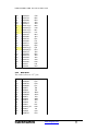
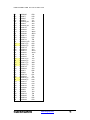
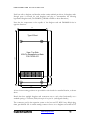
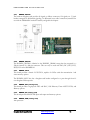
LOGIC Emulation Source
Daughtercard Interface
Description
D A U G H T E R C A R D
S P E C I F I C A T I O N
1 Dini Group Meg-Array Daughter card Interface
This file describes the Dini Group’s standard daughter card interface. The interface provides
186 signals from a host board to a daughter card. These signals are high-speed, flexible and
differentially capable.
The daughter card interface is built around a 400-pin FCI “MegArray” connector. This BGA
array of pins is designed for high-speed high-density board-to-board connections.
The “Plug” of the system is located on the host, and the “receptacle” is located on the
expansion board. This selection was made to give a greater height selection to the daughter card
designer.
The user typically designs his own daughter card with interfaces required for the emulation
project. The Dini Group is happy to review daughter card designs intended for interface to a
Dini Group host for possible compatibility problems. A daughter card designer should use the
schematic of the host board (provided with the board) to verify his design.
1.1 Banking System
To allow flexibility to the daughter card designer, the daughter card interface is divided into
three “Banks”. Each bank can have it’s own VCCO power, VREF (threshold voltage) and
source-synchronous IO clocking. Each bank contains 62 user IO signals (can be used as 31
differential pairs). Eight of these signals can be used as a source-synchronous clock into the host
FPGA. Four of these signals can be used as a reference voltage to the host fpga for standards
requiring a reference voltage.
The banks are named B0, B1 and B2, and every user IO on the header interface corresponds to
one of these banks. The signals name given to each user IO pin contains either “B0”, “B1”, or
“B2” in the name.
Other connections on the daughter card connector system (not correlated to a bank) include
three dedicated, differential clock connections for inputting global clocks from an external
source, power connections, bank VCCO power, a buffered power on reset signal.
1.2 Non-Compliant Boards
See section 4.2 of this guide for deviations from this specification.
2 Daughter Card Electrical
The daughter card pin out and routing were designed to allow use of the Virtex-4’s 1 Gbps
general purpose IO. The connector itself is capable of as high as 10Gbs transmission rates using
differential signaling. All signals on the host are all routed as differential, 50-Ohm transmission
lines, with means to properly terminate. All signals are routed against a ground plane, so for the
best signal integrity, should be routed against a ground plane on the daughter card with excellent
Daughter Card Specification
www.dinigroup.com
2
D A U G H T E R C A R D
S P E C I F I C A T I O N
IO voltage bypassing close to the terminus. When signals are used differentially, the trace
impedance is 100-ohms.
Signals on the host are not length-matched, except for each signal in a differential pair, which
are. Differential pairs are routed in parallel, but not closely coupled to make single-ended
signaling possible. Using the IDELAY and ODELAY (Stratix devices adaptive delay) elements
on the FPGA, the skew between mismatched signals can be corrected.
Most pins are assigned in a GSG pattern to minimize crosstalk. Some signals are arranged in a
GSSG pattern. (Pins in column E and F)
2.1.1
DCI
Host boards whose FPGAs that have DCI (digitally controlled impedance) capabilities have
DCI enabled with a 50-ohm reference resistor. This allows LVCMOS_DCI and SSTL_DCI IO
standards to be used.
2.2 Daughter card Signals
Bank 0 (VCCO0) includes the signals BL[0-31].
Bank 1 (VCCO1) includes B1L[0-31].
Bank 2 (VCCO2) includes signals B2L[0-31]
Special purpose pins are described below.
2.2.1
Clock Outputs
These signals are used for sending a clock signal (differential) from the daughter card to the
host.
The pair GCAP/GCAN (Pairs E1, F1) can be used as a SSTL18, SSTL25, LVDS differential
pair, or GCAP can be used single-endedly as LVCMOS25. These signals only connect to the
FPGA associated with the connector.
The pair GCBP/GCBN (E3, F3) can be used as a SSTL18, SSTL25, LVDS differential pair, or
GCAP can be used single-endedly as LVCMOS25. These signals only connect to the FPGA
associated with the connector.
The pair GCCP/GCCN (Pair E5, F5) must be used as an LVDS pair. This differential clock is
buffered and distributed to every FPGA on the host. This clock may be de-skewed on the host
through a zero-delay buffer. If this is the case (DN7000K10PCI, DN8000K10,
DN9000K10PCI) there may be special frequency requirements or settings for the buffers to
work. See the user manual for the specific board for these requirements. This clock network
may also be multi-purpose, so a setting may have to be used to enable this clock distribution.
2.2.2
User IO
User IO signals connect directly to a general-purpose IO site on the host FPGA. These signals
can be used as any drive standard supported by the host FPGA. Each bank must share VCCIO
and VREF requirements. For example, if bank B0 is supplied 1.8V by the daughter card on
Daughter Card Specification
www.dinigroup.com
3
D A U G H T E R C A R D
S P E C I F I C A T I O N
ALL of the VCCIO_B0 pins, and supplies 0.9V to ALL of the VREF_B0 pins, then the
daughter card may use each of the user IO pins as 1.8V SSTL inputs or outputs, LVDS outputs,
1.8V LVCMOS inputs or outputs, since all of these signal standards’ requirements are met.
User IO signals can be used single-endedly, or differentially. Differential pairs are pre-selected.
Each set of signals whose signal names differ only by a “p” or “n” in the signal name can be
used as differential pairs. For example, the signals
B2_L4p and B2_L4n can be used as a differential pair. These two signals are matched in length.
2.2.3
IO Clock
Some of the signals connected to the daughter card expansion headers are “clock-capable”; the
inputs on the host FPGA can be used for source-synchronous clocking. On Virtex-4 devices,
these pins have “CC” in the name. The CC pins on each bank are suitable for IO, sourcesynchronous clocking for all signals on that bank. A CC clock can only be used to clock signals
on the bank associated with it.
If source-synchronous clocking is not required, these signals can be used as “User IO”. On
Virtex-4 (DN8000K10 series) the host cannot drive LVDS signals on these pins, due to a
hardware constraint.
2.2.4
VREF
Pins declared as “VREF” pins by Xilinx have a defined placement on the daughter card pin out
to allow the daughter card to define a logic threshold as required by some standards. If you want
to use a standard with a VREF (SSTL15, SSTL15, SSTL18, HSTL15, HSTL18,
HSLVCMOS33) the daughter card should supply this reference voltage on these pins. For
optimal performance, capacitors should be installed on the host board on these signals near the
host’s FPGAs. Space provisions for these capacitors have been provided.
If VREF is not required by the intended signaling standard, then these signals can be used as
“User IO” without restriction.
2.2.5
Power
The +3.3V, +5.0V and +12V power rails are supplied to the Daughter card headers. Each pin
on the MegArray connector is rated to tolerate 1A of current without thermal overload. Most of
the power available to daughter cards through the connector comes from the two 12V pins, for
a total of 24W. The host provides a fuse on each of these rails.
2.2.6
IO Power
The signaling standard of the daughter card is left undefined by the host. For a standard to be
used, the daughter card should supply power to the VCCIO pins of the daughter card
connector. The pins are connected directly to the VCCIO power pin on the host FPGA. Each
of the three banks on the daughter card has two VCCIO pins. Each of the three banks can have
its VCCIO set independently, but both pins on a bank must be the same voltage. The daughter
card should be able to supply enough current to the host FPGA to power the entire bus. The
daughter card designer will need to calculate the host FPGA’s current requirements.
Daughter Card Specification
www.dinigroup.com
4
D A U G H T E R C A R D
S P E C I F I C A T I O N
When the daughter card does not supply a voltage the host, the host will power these pins at
1.2V with a minimal current capacity. The daughter card can overdrive this voltage safely.
2.2.7
Reset
The reset signal (Active low) is an open-drain, buffered copy of the reset signal on the host. This
signal is asserted when the host power is not within tolerance. The signal must be pulled up on
the daughter card with a resistor. When the reset signal is active, the FPGAs on the host will not
be configured.
F7
7A
+5.0V
F6
5A
+12.0V
F5
5A
P100- 1
A1
K1
C1
H1
2
DC_RSTn
1
B2
D2
G2
+3.3V
U254
A
VCC
O.D.
Y
NC
GND
5
4
3
74LVC 1G 07
SOT95P280- 5N
DC0_RSTn
J2
P12V_1
P12V_2
P5V_1
P5V_2
P3.3V_1
P3.3V_2
P3.3V_3
GCAP
GCAN
1A PER PIN
+3.3V
GCBP
GCBN
GCC P
GCC N
E1
F1
E3
F3
E5
F5
DC0_GCAP 104
DC0_GCAN 104
DC0_GCBP 104
DC0_GCBN 104
DC0_GCC P 85
DC0_GCC N 85
RSTn
Section 1 of 5
Clock, Power, Reset
MEG -Ar ray 300-Pi n
The RSTn signal to the daughter card is an open-drain, buffered copy of the SYS_RSTn signal.
This signal causes the entire DN8000K10 to reset, losing all FPGA configuration data and
resetting the configuration circuitry.
2.3 Pin out
The following lists are the pin assignments to the MEG Array connector. The pins are labeled as
in the FCI connector part drawing.
2.3.1
Clock and Reset Signals
F1
E1
GCAP
GCAN
E3
F3
GCBP
GCBN
E5
F5
GCCP
GCCN
J2
RSTn
Daughter Card Specification
www.dinigroup.com
5
D A U G H T E R C A R D
2.3.2
Power Signals
A1
K1
+12V
+12V
C1
H1
+5V
+5V
B2
D2
G2
+3.3V
+3.3V
+3.3V
2.3.3
A10
A12
A14
A16
A18
A2
A22
A24
A26
A28
A30
A34
A36
A38
A4
A40
A8
2.3.4
S P E C I F I C A T I O N
Ground Signals
B3
B1
B13
B11
B5
B9
B7
B23
B21
B15
B19
B27
B25
B17
B29
B31
B33
B35
B37
B39
C14
C22
C8
C2
C24
C4
C10
C18
C16
C6
C20
C12
C26
C28
C30
C32
C34
C36
C38
C40
D1
D11
D13
D15
D17
D19
D21
D23
D25
D27
D29
D3
D31
D33
D35
D37
D39
D5
D7
D9
E10
E12
E14
E16
E18
E2
E20
E22
E24
E26
E28
E30
E32
E34
E36
E38
E4
E40
E6
E8
F10
F12
F14
F16
F18
F2
F20
F22
F24
F26
F28
F30
F32
F34
F36
F38
F4
F40
F6
F8
G1
G11
G13
G15
G17
G19
G21
G23
G25
G27
G29
G3
G31
G33
G35
G37
G39
G5
G7
G9
K10
K12
K14
K16
K18
K2
K22
K24
K26
K28
K30
K34
K36
K38
K4
K40
K8
J1
J11
J13
J15
J17
J19
J21
J23
J25
J27
J29
J3
J31
J33
J35
J37
J39
J5
J7
J9
H10
H12
H14
H16
H18
H2
H20
H22
H24
H26
H28
H30
H32
H34
H36
H38
H4
H40
H6
H8
Bank B0 IO
Pins shaded yellow are “CC” pins
A3
B4
C3
D4
H3
G4
K3
J4
A5
DCC0P1
DCC0N1
DCC0P2
DCC0N2
DCC0P3
DCC0N3
DCC0P4
DCC0N4
DCC0P5
N22
N23
H29
H30
N27
P27
K32
K33
M25
Daughter Card Specification
www.dinigroup.com
6
D A U G H T E R C A R D
B6
C5
D6
H5
G6
K5
J6
A7
B8
C7
D8
E7
F7
H7
G8
K7
J8
A9
B10
C9
D10
E9
F9
H9
G10
K9
J10
A11
B12
C11
D12
E11
F11
H11
G12
K11
J12
A13
B14
C13
D14
E13
F13
H13
G14
K13
J14
A15
S P E C I F I C A T I O N
DCC0N5_VR
DCC0P6
DCC0N6
DCC0P7
DCC0N7
DCC0P8
DCC0N8_VR
DCC0P9
DCC0N9_VR
DCC0P10
DCC0N10
DCC0P26
DCC0N26
DCC0P11
DCC0N11
DCC0P12
DCC0N12_VR
DCC0P13_C
DCC0N13_C
DCC0P14
DCC0N14
DCC0P27
DCC0N27
DCC0P15
DCC0N15
DCC0P16_C
DCC0N16_C
DCC0P17_C
DCC0N17_C
DCC0P18
DCC0N18
DCC0P28
DCC0N28
DCC0P19
DCC0N19
DCC0P20_C
DCC0N20_C
DCC0P21
DCC0N21
DCC0P22
DCC0N22
DCC0P29
DCC0N29
DCC0P23
DCC0N23
DCC0P24
DCC0N24
DCC0P25
M26
J27
K27
G32
G33
M30
M31
H32
J32
C32
D32
J34
K34
K28
K29
N25
P26
D34
E34
H27
H28
N29
N30
F33
F34
R22
R23
L30
L31
L28
L29
L33
L34
J29
J30
G30
G31
P24
R24
M27
M28
M32
M33
P22
R21
E32
E33
H33
Daughter Card Specification
www.dinigroup.com
7
D A U G H T E R C A R D
B16
C15
D16
F15
E15
DCC0N25
DCC0P0
DCC0N0
DCC0N30
DCC0P30
2.3.5
Bank B1 IO
S P E C I F I C A T I O N
H34
P20
R19
C34
C33
Pins shaded yellow are “CC” pins
H15
G16
K15
J16
A17
B18
C17
D18
E17
F17
H17
G18
K17
J18
A19
B20
C19
D20
E19
F19
H19
G20
K19
J20
A21
B22
C21
D22
E21
F21
H21
G22
K21
J22
A23
B24
C23
DCC1P1
DCC1N1
DCC1P2
DCC1N2
DCC1P3
DCC1N3
DCC1P4
DCC1N4
DCC1P26
DCC1N26
DCC1P5
DCC1N5
DCC1P6
DCC1N6
DCC1P7
DCC1N7_VR
DCC1P8
DCC1N8
DCC1P27
DCC1N27
DCC1P9
DCC1N9
DCC1P10
DCC1N10_VR
DCC1P11
DCC1N11_VR
DCC1P12
DCC1N12
DCC1P28
DCC1N28
DCC1P13
DCC1N13
DCC1P14
DCC1N14_VR
DCC1P15_C
DCC1N15_C
DCC1P16
B21
A21
E28
F28
A30
B30
K24
J24
D24
D25
G27
G28
D30
D31
C29
C30
C22
B22
D29
E29
J25
K26
F29
F30
G25
H25
F25
F26
L25
L26
B25
C25
D27
E27
A31
B31
C23
Daughter Card Specification
www.dinigroup.com
8
D A U G H T E R C A R D
D24
E23
F23
H23
G24
K23
J24
A25
B26
C25
D26
E25
F25
H25
G26
K25
J26
A27
B28
C27
D28
H27
G28
K27
J28
2.3.6
DCC1N16
DCC1P29
DCC1N29
DCC1P17
DCC1N17
DCC1P18_C
DCC1N18_C
DCC1P19_C
DCC1N19_C
DCC1P20
DCC1N20
DCC1P30
DCC1N30
DCC1P21
DCC1N21
DCC1P22_C
DCC1N22_C
DCC1P23
DCC1N23
DCC1P24
DCC1N24
DCC1P25
DCC1N25
DCC1P0
DCC1N0
S P E C I F I C A T I O N
C24
B32
B33
A28
A29
B28
C28
B27
C27
B23
A23
E31
F31
D26
E26
F23
E23
A26
B26
A24
A25
G23
H24
F24
E24
Bank B2 IO
Pins shaded yellow are “CC” pins
E27
F27
A29
B30
C29
D30
E29
F29
H29
G30
K29
J30
A31
B32
C31
D32
E31
DCC2P28
DCC2N28
DCC2P30
DCC2N30
DCC2P2
DCC2N2
DCC2P29
DCC2N29
DCC2P3
DCC2N3
DCC2P4
DCC2N4
DCC2P5
DCC2N5_VR
DCC2P6
DCC2N6
DCC2P25
N32
P32
P30
P31
T24
T25
AB31
AA31
Y29
W29
W27
V27
R27
R28
T23
U23
P29
Daughter Card Specification
www.dinigroup.com
9
D A U G H T E R C A R D
F31
H31
G32
K31
J32
A33
B34
C33
D34
E33
F33
H33
G34
K33
J34
A35
B36
C35
D36
E35
F35
H35
G36
K35
J36
A37
B38
C37
D38
E37
F37
H37
G38
K37
J38
A39
B40
C39
D40
E39
F39
H39
G40
K39
J40
S P E C I F I C A T I O N
DCC2N25
DCC2P7
DCC2N7
DCC2P8
DCC2N8_VR
DCC2P9
DCC2N9_VR
DCC2P10
DCC2N10
DCC2P26
DCC2N26
DCC2P11
DCC2N11
DCC2P12
DCC2N12_VR
DCC2P13_C
DCC2N13_C
DCC2P14
DCC2N14
DCC2P27
DCC2N27
DCC2P15
DCC2N15
DCC2P16_C
DCC2N16_C
DCC2P17_C
DCC2N17_C
DCC2P18
DCC2N18
DCC2P1
DCC2N1
DCC2P19
DCC2N19
DCC2P20_C
DCC2N20_C
DCC2P21
DCC2N21
DCC2P22
DCC2N22
DCC2P0
DCC2N0
DCC2P23
DCC2N23
DCC2P24
DCC2N24
R29
U30
U31
Y31
W31
V28
V29
W32
V32
AB32
AB33
U26
U27
T28
U28
N33
N34
V23
V24
AA33
AA34
T33
T34
Y32
Y33
W30
V30
V33
V34
R26
T26
R31
T31
P34
R34
U32
U33
V25
U25
Y27
Y28
T29
T30
R32
R33
Daughter Card Specification
www.dinigroup.com
10
D A U G H T E R C A R D
2.3.7
S P E C I F I C A T I O N
VCCIO Signals
VCCO corresponds to bank B0, VCC1 corresponds to bank B1, VCC2 corresponds to bank
B2.
K6
A6
VCCO0
VCCO0
K20
A20
VCCO1
VCCO1
A32
K32
VCCO2
VCCO2
Daughter Card Specification
www.dinigroup.com
11
D A U G H T E R C A R D
S P E C I F I C A T I O N
Daughter Card Specification
www.dinigroup.com
12
D A U G H T E R C A R D
S P E C I F I C A T I O N
2.4 VCCO bias generation
Since a daughter card will not always be present on a daughter card connector, a VCCO bias
generator is used on the motherboard for each daughter card bank to keep the VCCO pin on
the FPGA within its recommended operating range. The VCCO bias generators supply +1.2V
to the VCCO pins on the FPGAs, and are back-biased by the daughter card when it drives the
VCCO rails.
The VCCO voltage impressed by the daughter card should be less than 3.75 to prevent
destruction of the Virtex 4 IOs connected to that daughter card.
+5.0V
U271
8
5
3
6
7
IN
OUT
1
SHDN #
DC0_B0_VCCO
C1803
0.01uF
R452
0
380mA MAX
AT 1.22V
GND 1
GND 2
BYP
GND 3
ADJ
4
2
Vadj = 1.22V
LT1763CS8
SOIC127P600-8N
R467
10.0K
380mA MAX AT 1.22V
3 Daughter card Mechanical
Daughter card expansion headers are located on the bottom side of the PWB. This is done to
eliminate the need for resolving board-to-board clearance issues, assuming the daughter card
uses no large components on the backside.
Daughter Card Specification
www.dinigroup.com
13
D A U G H T E R C A R D
S P E C I F I C A T I O N
Each host with a daughter card interface makes certain minimal provisions for daughter cards.
Enough space is reserved for each daughter card plug to accommodate the following
hypothetical daughter card. (The DNMEG_OBS400 conforms to these dimensions)
Note that the components on the topside of the daughter card and DN8000K10 face in
opposite directions.
2.75"
View: Top Side
400-Pin Receptacle on Back
P/N: 74390-101
View: Top Side
300-Pin Receptacle on Back
P/N: 84553-101
5.000"
Type 0/1/4 Short
4.250"
Type 2 Short
3.250"
5.000"
2.75"
A1
1.950"
0.750"
0.500"
A1
0.500"
1.950"
At least four mounting positions are provided for each header in a standard location, as shown
above.
Boards that have multiple daughter card connectors next to each other (horizontally) use a
standard spacing of 78.25mm (3.08in) from pin A1 to pin A1. (and aligned vertically)
The connectors used in the expansion system on the host are FCI MEG-Array 400-pin plug,
6mm, part #84520-102. A suitable mating connector for use on a daughter card would be FCI
Daughter Card Specification
www.dinigroup.com
14
0.500"
D A U G H T E R C A R D
S P E C I F I C A T I O N
part 74390-101 (lead-free 74390-101LF). This provides the minimum board-to-board spacing.
Other spacings are possible with different connectors on the daughter card.
3.1.1
Daughter card mounting DN8000K10
The DN8000K10 features a standard metal base plate that gives the board mechanical stability,
and provides plenty of mounting points for daughter cards. The daughter card receptacle on the
daughter card itself will also be mounted on the backside of the board.
Daughter Card
Mated
Height
14mm
RECEPT
Shield
PLUG
0.200"
Motherboard
The daughter card should use standoffs to secure itself to the backside of the base plate. The
standard chassis that comes with the DN8000K10 will allow it to operate FPGA side down, or
on its side to allow physical access to the daughter card and the controls of the DN8000K10.
With this host-plate-daughter card arrangement, there is a limited Z dimension clearance for
backside components on the daughter card. This dimension is determined by the daughter card
designer’s part selection for the MegArray receptacle.
3.1.2
Insertion and removal
Due to the small dimensions of the very high speed MegArray connector system, the pins on
the plug and receptacle of the Meg Array connectors are very delicate.
When plugging in a daughter card, make sure to align the daughter card first before pressing on
the connector. Be absolutely certain that both the small and the large keys at the narrow ends of the Meg Array
line up BEFORE applying pressure to mate the connectors!
Daughter Card Specification
www.dinigroup.com
15
D A U G H T E R C A R D
S P E C I F I C A T I O N
Place it down flat, then press down gently.
The following two excerpts are taken from the FCI application guide for the Meg Array series of
connectors.
A part can be started from either end. Locate and match the connector’s A1 position marking (“?”) for
both the Plug and Receptacle. (Markings are located on the long side of the housing.) Rough alignment
is required prior to connector mating as misalignment of >0.8mm could damage connector contacts.
Rough alignment of the connector is achieved through matching the Small alignment slot of the plug
housing with the Small alignment key of the receptacle housing and the Large alignment slot with the
Large alignment key. Both connector housings have generous lead-in around the perimeter and will
allow the user to blind mate assemble the connectors. Align the two connectors by feel and when the
receptacle keys start into the plug slots, push down on one end and then move force forward until the
receptacle cover flange bottoms on the front face of the plug.
Dec 09, 2004
Like mating, a connector pair can be unmated by pulling them straight apart. However, it requires less
effort to un-mate if the force is originated from one of the slot/key ends of the assembly. (Reverse
procedure from mating) Mating or un-mating of the connector by rolling in a direction perpendicular to
alignment slots/keys may cause damage to the terminal contacts and is not recommended.
4 Dini Group products
4.1 Board List
The following boards comply with this document’s header specifications:
Daughter Card Specification
www.dinigroup.com
16
D A U G H T E R C A R D
S P E C I F I C A T I O N
DN7000K10PCI
DN8000K10
DN8000K10PSX
DNMEG_S2GX
3 Headers
11 Headers (7 are non-standard)
1 Header
1 Header
Coming Soon:
DN9000K10PCI
DNMEG_ADC
3 Headers
1 Header
4.2 Exceptions
The following products have headers that do not fully comply with these specification. A list of
exceptions to this specification follows, with a description of the deviation.
4.2.1
DN8000K10PSX
GCCP/GCCN is not deskewed on the host. FPGAs on the host will receive this signal
synchronized with respect to each other, but with no phase relationship with the daughter card.
4.2.2
DN8000K10
Daughter cards D0, D1, D2, D3, D4, D9 use 300-pin Meg Array connectors instead of 400-pin.
The signal definitions remain the same, except that pin rows 29-40 are not present, and the
connector supports two banks (B0, B1) instead of three.
DC0 and DC3 do not comply with these specifications. See the DN8000K10 user guide and
schematic. (These headers are used for RocketIO signaling) These signals are routed as 110-ohm
differential pairs, instead of 100-Ohm.
DC10 is reserved for Dini Group use and should not be used for a custom daughter card
without the cooperation of Dini Group.
4.2.3
DN7000K10PCI
Banks B0 and B1 must be set to the same VCCIO voltage. These two nets are connected on the
host.
4.2.4
DNMEG_S2GX
Note that only DC_TOP (P4) is a daughter card header that complies with this specification. P5
is the receptacle for a host board.
4.2.5
DN9000K10
On headers DC4 and DC9, VCCO is shared between some banks. See the User Manual for a
complete description of this deviation.
4.3 Standard Daughter cards
The Dini Group has some general-purpose daughter cards available. See the Dini Group
website for more information.
Daughter Card Specification
www.dinigroup.com
17
D A U G H T E R C A R D
4.3.1
S P E C I F I C A T I O N
DNMEG_OBS400
The breakout daughter card provides 48 signals on Mictor connector, 124 signals on .1” pitch
headers arranged for differential signaling, 14 differential coax cable connection (intended for
use with the DN8000K10 rocketIO headers) and global clock inputs.
4.3.2
DNMEG_OBS300
The DNMEG_OBS300 is identical to the DNMEG_OBS400 except that the receptacle is a
300-pin instead of a 400-pin connector. This can only be used with DC0, DC1, DC2, DC3,
DC4, DC9 on the DN8000K10.
4.3.3
DNMEG_S2GX
This board provides a Stratix 2 GX FPGA, capable of 6.5Gbs serial data transmission. And
some memory options.
The DNMEG_S2GX also has a daughter card header configured as a pass-through from it’s
own daughter card receptacle.
4.3.4
DNMEG_ADC (coming soon)
This board provides a high-speed ADC and DAC, 1Gb Ethernet, Virtex-4 SX55 FGPA, and
Memory options.
4.3.5
DNMEG_DVI (coming soon)
This board provides dual DVI-D input and output and memory options.
4.3.6
DNMEG_ARM (coming soon)
Arm processor
Daughter Card Specification
www.dinigroup.com
18
D A U G H T E R C A R D
4.3.7
S P E C I F I C A T I O N
DNMEG_PROTO (coming soon)
Prototype area
Daughter Card Specification
www.dinigroup.com
19