1
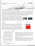
GS-2 5 2 5 GS-2525 User Manual Version 1.0 2007/09/29 HangZhou KinCony Electronics CO.,LTD Fax: 0571-88009850-3 Http://www.hificat.com GS-2 5 2 5 Figure List ................................................................................................................................ II Table List ................................................................................................................................. III 1 2 Introduction ..................................................................................................................... 4 1.1 Product applications ..................................................................................... 4 1.2 Product Picture .............................................................................................. 5 1.3 GS-2525 Series Block Diagram ................ ............................................. 7 1.4 GS-2525 Technique Specification............. ............................................ 8 1.5 Application Circuit......................................................................................... 9 1.6 Recommended layout PAD..........................................................................11 1.7 Mechanical Layout ...................................................................................... 12 1.8 GS-2525-Test Software Specification......... 1.9 Hardware interface ...................................................................................... 13 Software Interface ......................................................................................................... 17 2.1 3 ......................................... 12 NMEA V3.0 Protocol .................................................................................... 17 2.1.1 GGA-Global Positioning System Fixed Data ................................... 17 2.1.2 GLL-Geographic Position –Latitude/Longitude............................... 18 2.1.3 GSA-GNSS DOP and Active Satellites .............................................. 19 2.1.4 GSV-GNSS Satellites in View ............................................................. 19 2.1.5 RMC-Recommended Minimum Specific GNSS Data ....................... 20 2.1.6 VTG-Course Over Ground and Ground Speed ................................ 21 GPS Receiver User’s Tip .............................................................................................. 22 3.1 Package Specification and Order Information ......................................... 23 3.2 Lead-Free Standard Reflow Profile............................................................ 23 4 Contact Information Section........................................................................................ 24 5 Revision History............................................................................................................ 24 I GS-2 5 2 5 Figure List Figure 1-1 GS-2525 Front View ................... ............................................................ 5 Figure 1-2 GS-2525 Interface Board Front View... ................................................. 5 Figure 1-3 Evaluation Kit Front View............................................................................. 7 Figure 1-4 System Block Diagram ................................................................................. 7 Figure 1-5 Application Circuit Reference...................................................................... 9 Figure 1-6 Recommended Layout Pad.........................................................................11 Figure 1-7 Mechanical Layout ...................................................................................... 12 Figure 1-8 Hardware Interface...................................................................................... 13 Figure 3-1 Package Specifications .............................................................................. 23 II GS-2 5 2 5 Table List Table 1-1 The interface board pin definition................................................................. 5 Table 1-2 Technical Specifications ................................................................................ 8 Table 1-3 Definition of Pin assignment ....................................................................... 13 Table 2-1 NMEA-0183 Output Messages ..................................................................... 17 Table 2-2 GGA Data Format .......................................................................................... 17 Table 2-3 Position Fix Indicators ................................................................................. 18 Table 2-4 GLL Data Format ........................................................................................... 18 Table 2-5 GSA Data Format .......................................................................................... 19 Table 2-6 Mode 1............................................................................................................ 19 Table 2-7 Mode 2............................................................................................................ 19 Table 2-8 GGA Data Format .......................................................................................... 20 Table 2-9 GGA Data Format .......................................................................................... 20 Table 2-10 VTG Data Format......................................................................................... 21 III GS-2 5 2 5 1 Introduction Gstar GS-2525 low power and small form factor board is the newest generation of Gstar GPS module. The module is pow ered by latest SiRF Star III single chip and Gsatr proprietary navigation technol ogy that provides you with stable and accurate navigation data. The smallest form factor and miniature design is the best choice to be embedded in a device such as portable navigation device, personal locator, speed camera detector and vehicle locator. Product Features 20 parallel channels SMT type with stamp holes TCXO design 0.1 second reacquisition time Small form factor with embedded SiRF Star III single chip technology. NMEA-0183 compliant protocol/customize protocol. Enhanced algorithm for navigation stability Excellent sensitive for urban canyon and foliage environments. DGPSBAS (WAAS, EGNOS and MSAS) support Auto recovery while RTC crashes Trickle power supported Build-in LNA and saw filter 1.1 Product applications Automotive navigation Personal positioning and navigation Marine navigation Timing application 4 GS-2 5 2 5 1.2 Product Picture GS-2525 Pin16 Pin 15 Pin 30 Pin 1 Figure 1-1 REB-3571LP Front View GS-2525 Interface Board(Compatible with REB-3300 interface board) Figure 1-2 GS-2525 Interface Board Front View Table 1-1 The interface board pin definition PIN GS --2520 GS - 2523 1 VCC V_GPS_3V3 VCC 2 GND GND GND 3 Bootselect Bootselect Bootselect 4 RXA RXA RXA 5 TXA TXA TXA 6 TXB TXB TXB 7 RXB RXB RXB 8 GPIO14 N.C. GPIO14 5 GS --2525 GS-2 5 2 5 9 RF-ON RF-ON RF-ON 10 GND GND GND 11 GND N.C. GND 12 GND N.C. GND 13 GND GND GND 14 GND N.C. GND 15 GND GND GND 16 GND GND GND 17 RF-IN GPS_RF_IN RF-IN 18 GND GND GND 19 V-ANT V-ANT_IN V-ANT 20 VCC-RF VCC_RF_OUT VCC-RF 21 V-BAT V_RTC_3V3 V-BAT 22 RESET-IN RESET RESET-IN 23 GPIO10 N.C. GPIO10 24 GPIO1 N.C. GPIO1 25 GPIO5 GPIO4 GPIO4 26 GPIO0 GPIO0 GPIO0 27 GPIO13 N.C. GPIO13 28 GPIO15 N.C. GPIO15 29 PPS PPS PPS 30 GND GND GND 31 NO PAD N.C. NO PAD 6 GS-2 5 2 5 1.3 GS-2525 Series Block Diagram GS-2525 engine board consists of SiRF star III singl e chipset technology; 4Mbits flash memory, and proprietary software. The system is described as follows. a. External antenna. b. 4 Mega bits flash memory c. 30 pin I/O pin Figure 1-5 System Block Diagram 7 GS-2 5 2 5 1.4 GS-2525 Technique Specification Impedance: :50Ω Ω Table 1-2 Technical Specifications No Function Specification GPS receiver 1 Chipset 2 Frequency SiRF Star III, GSC3f/LP (Digital, RF in a single package) L1 1575.42MHz. 3 Code C.A. Code. 4 Channels 20 parallel 5 Sensitivity (Acquisition) It shall show C/No ≧ 40 dB-Hz when external power = -130dBm. 6 Chip set cold start 35s @ open sky (Typical) 7 Chip set warm start 35s @ open sky (Typical) 8 Chip set hot start 1s @ open sky (Typical) 9 Reacquisition less than 1s 10 Position accuracy 10meters at 2D RMS. 11 Maximum altitude 18000 m 12 Maximum velocity 514 m/s 13 Trickle power mode Duty cycle ≦ 34%. (Variable) 14 Update rate Continuous operation: 1Hz 15 Testability It shall be able to be tested by SiRF test IV and single channel simulator. 16 Protocol setup It shall store the protocol setup in the SRAM memory. 17 DGPS WAAS, EGNOS Interface 18 LNA 15dB Gain. (Typical) 19 I/O Pin 30pin Power consumption 21 Vcc DC 3.3 ±5% 22 Current Avg. Acquisition <[email protected](without ext. antenna) Avg. Tracking<[email protected](without ext. antenna) Environment 23 Temperature Operating : -40 ~ 85℃ Storage : -40 ~ 85℃ 24 Humidity ≦95% 8 GS-2 5 2 5 1.5 Application Circuit J1 RF MCX JACK 5 3 4 R1 0 ohm R2 0 ohm 1 50 ohm Trace C1 OPEN 2 C2 OPEN +3.3V +3.3V U1 R7 0 ohm RF_IN R8 C7 0.1uF/X5R/16V OPEN V_RTC_3V3 RESET GPS_IO10 GPS_IO1 GPS_IO4 GPS_IO0 GPS_IO13 GPS_IO15 GPS_PPS +3.3V_BAT (Alway s) 1 3 C4 10uF /10V /Y 5V 2 D1 RB705D U2 3V 3.3mAH R6 470 ohm/ 5% 16 17 18 19 20 21 22 23 24 25 26 27 28 29 30 GND RF_IN GND V_ANT_IN VCC_RF_OUT V_RTC_3V3 RESET GPIO[10] GPIO[1] GPIO[4] GPIO[0] GPIO[13] GPIO[15] PPS GND GND GND GND GND GND GND RF_ON GPIO[14] RXB TXB TXA RXA Bootselect GND VCC_3V3 15 14 13 12 11 10 9 8 7 6 5 4 3 2 1 R3 OPEN(10K) RXB RF_ON GPS_IO14 R4 R5 220 RXB 220 GPS_Bootselect SY STEM_TXB SY STEM_RXB SY STEM_RXA SY STEM_TXA +3.3V VCC_3V3 GS-2525 C5 0.1uF/X5R/16V C6 10uF/Y 5V/10V + Figure 1-6 Application Circuit Reference Note: (1) Ground Planes: These pin(2,10~16、18、30) should be connect to ground. (2) Serial Interface: (Ⅰ) The TXA pin is the serial output data (Default NMEA) . (Ⅱ) The TXB pin is the serial output data (Default Null) . (Ⅲ) The RXA pin is the serial input data (Default NMEA) . (Ⅳ) The RXB pin is the serial input data (Default Null). (3) Backup Battery: When module is working, must to supply VCC_3V3(P1) and V_RTC_3V3 (P21) power at the same time. It’s recommended to connect a backup battery to V_RTC_3V3 pin. In order to enable the warm start and hot start features of the GPS receiver. If you use backup battery, should be add a bypassing capacitor (10uF) at V_RTC_3V3 pin. It can reduce noise and increase the stability. (4) RF_IN: Connecting to the antenna has to be routed on the PCB. The transmission line must to controlled impedance to connect RF_IN to the antenna or antenna connector of your choice. (Impedance 50Ω) (5) Power: Connect VCC_3V3 pin to DC +3.3V. The power supply must add bypassing capacitor (10uF and 0.1uF).It can reduce the Noise from power supply and 9 GS-2 5 2 5 increase power stability. (6) Active antenna bias voltage: The VCC_RF_OUT pin (pin 20) is provide voltage 2.85V. If you use active antenna, you can connect this pin to V_ANT_IN pin (pin 19) to provide bias voltage of active antenna. The bias voltage will be through GPS_RF_IN pin to provide active antenna bias voltage from Vcc_RF_OUT pin. If your bias voltage of active antenna isn’t 2.85V, you can input bias voltage to V_ANT_IN pin (pin 19).And input bias voltage of you need. The input bias voltage will through GPS_RF_IN pin to provide active antenna bias voltage from V_ANT_IN pin. PS: (1) The maximum power consumption of active antenna is about 85mW. (2) The input gain ranges are 19~ 22dB. (7) GPIO: The GPIO pin is recommended to connect to serial resistance(220Ω),if use the GPIO function. If no use GPIO functions, it doesn’t connect anything. 10 GS-2 5 2 5 1.6 Recommended layout PAD Figure 1-7 Recommended Layout Pad 11 GS-2 5 2 5 1.7 Mechanical Layout Figure 1-8 Mechanical Layout 1.8 GS-2525-Test Software Specification No Function Specification 1 Clock offset 88000Hz≦量測值≦104000Hz 2 Clock Drift 量測值≦200Hz 3 C/No Hi Power Mean 量測值≧39dB 4 C/No Hi Power Sigma 量測值≦2dB 5 Bit Sync 量測值≦5 Sec 6 Frame Sync 量測值≦28 Sec 7 Phase Error 量測值≦0.22 8 RTC 測試 RTC Frequency 測試 31000≦量測值≦33500 可靠性及品質目標 MTBF > 10000 hours. 12 GS-2 5 2 5 1.9 Hardware interface Figure 1-9 Hardware Interface Table 1-3 Definition of Pin assignment Pin Signal Name I/O Description Characteristics I DC +3.3V±5% # 1 VCC_3V3 DC Supply Voltage input 2 GND G Ground Reference Ground 3 Bootselect I Boot mode 3.15V ≥ VIH ≥ 2.0V - 0.3V ≤ VIL ≤ 0.86V 4 RXA I Serial port A 5 TXA O Serial port A 3.15V ≥ VIH ≥ 2.0V 2.85V ≥ VOH ≥ 2.14V - 0.3V ≤ VIL ≤ 0.86V VOL ≤ 0.71V 6 TXB O Serial port B 2.85V ≥ VOH ≥ 2.14V 7 RXB I Serial port B 3.15V ≥ VIH ≥ 2.0V - 0.3V ≤ VIL ≤ 0.86V 8 GPIO[14] I/O General purpose I/O 3.15V ≥ VIH ≥ 2.0V 2.85V ≥ VOH ≥ 2.14V - 0.3V ≤ VIL ≤ 0.86V VOL ≤ 0.71V Indicates VOH = 2.85V 9 RF_ON O power state of RF part 10 GND G Ground Reference Ground 11 G Ground Reference Ground GND 13 VOL ≤ 0.71V VOL = 0V GS-2 5 2 5 12 GND G Ground Reference Ground 13 GND G Ground Reference Ground 14 GND G Ground Reference Ground 15 GND G Ground Reference Ground 16 GND G Ground Reference Ground 17 RF_IN I GPS Signal 50 Ω @1.57542GHz input 18 GND G Ground Reference Ground 19 V_ANT_IN I Active Receiving DC power supply for active antenna Antenna Bias bias. voltage 20 VCC_RF_OUT O Supply DC +2.85V ±2% Antenna Bias Current<30mA voltage 21 V_RTC_3V3 I Backup 22 Reset I Reset (Active VIH > 2.3V V IL < 0.8V DC + 2.5 ~ +3.6V voltage supply Current ≤ 10uA low) 23 GPIO[10] I/O General purpose I/O 24 GPIO[1] I/O General purpose I/O 25 GPIO[4] I/O General purpose I/O 26 GPIO[0] I/O General purpose I/O 27 GPIO[13] I/O General purpose I/O 28 GPIO[15] I/O General purpose I/O 29 PPS O 3.15V ≥ VIH ≥ 2.0V 2.85V ≥ VOH ≥ 2.14V - 0.3V ≤ VIL ≤ 0.86V VOL ≤ 0.71V 3.15V ≥ VIH ≥ 2.0V 2.85V ≥ VOH ≥ 2.14V - 0.3V ≤ VIL ≤ 0.86V VOL ≤ 0.71V 3.15V ≥ VIH ≥ 2.0V 2.85V ≥ VOH ≥ 2.14V - 0.3V ≤ VIL ≤ 0.86V VOL ≤ 0.71V 3.15V ≥ VIH ≥ 2.0V 2.85V ≥ VOH ≥ 2.14V - 0.3V ≤ VIL ≤ 0.86V VOL ≤ 0.71V 3.15V ≥ VIH ≥ 2.0V 2.85V ≥ VOH ≥ 2.14V - 0.3V ≤ VIL ≤ 0.86V VOL ≤ 0.71V 3.15V ≥ VIH ≥ 2.0V 2.85V ≥ VOH ≥ 2.14V - 0.3V ≤ VIL ≤ 0.86V VOL ≤ 0.71V One pulse per 3.15V ≥ VIH ≥ 2.0V second 30 GND G Ground Reference Ground Definition of Pin assignment .VCC_3V3 (+3.3V DC power Input) 14 - 0.3V ≤ VIL ≤ 0.86V GS-2 5 2 5 This is the DC power supply input pin for GPS system. It provides voltage to module. .GND GND provides the ground . .Boot Set this pin to high for programming flash. .RXA This is the main receiver channel and is used to receive software commands to the board from SIRFdemo software or from user written software. .RXB This is the auxiliary receiving channel and is used to input differential corrections to the board to enable DGPS navigation. .TXA This is the main transmitting channel and is used to output navigation and measurement data to SiRFdemo or user written software. .TXB For user’s application (not currently used). .RF_ON This pin indicates state of RF voltage. .GPS_RF_IN This pin receives GPS analog signal. The line on the PCB between the antenna(or antenna connector) has to be a controlled impedance line (Microstrip at 50Ω). .V_ANT_IN This pin is reserved as external DC power supply input for active antenna. If using 2.85V active antenna, pin 20 has to be connected to pin 19. If using 3.3V or 5V active antenna ,this pin has to be connected to 3.3V or 5V power supply. PS: The current must be ≦100mA and voltage ≦12V,if using external power supply. .VCC_RF_OUT This pin can provide power [email protected] for active antenna. .Reset This pin provides an active-low reset input to the board. It causes the board to reset and start searching for satellites. If not utilized, it may be left open. .PPS This pin provides one pulse-per-second output from the board, which is synchronized to GPS time. This is not available in Trickle Power mode. .V_RTC_3V3 (Backup battery) 15 GS-2 5 2 5 This is the battery backup input that powers the SRAM and RTC when main power is removed. Typical current draw is 10uA. The supply voltage should be between 2.5V and 3.6V. .GPIO Functions Several I/Os are connected to the digital interface connector for custom applications. 16 GS-2 5 2 5 2 Software Interface 2.1 NMEA V3.0 Protocol Its output signal level is TTL: 4800 bps (default), 8 bit data, 1 stop bit and no parity. It supports the following NMEA-0183 Messages: GGA, GLL, GSA, GSV, RMC and VTG. NMEA Output Messages: the Engine board outputs the following messages as shown in Table 2-1: Table 2-1 NMEA-0183 Output Messages NMEA Record Description GGA Global positioning system fixed data GLL Geographic position – latitude / longitude GSA GNSS DOP and active satellites GSV GNSS satellites in view RMC Recommended minimum specific GNSS data VTG Course over ground and ground speed 2.1.1 GGA-Global Positioning System Fixed Data Table 2-2 contains the values of the following example: $GPGGA, 161229.487, 3723.2475, N, 12158.3416, W, 1, 07, 1.0, 9.0, M, , , ,0000*18 Table 2-2 GGA Data Format Name Example Units Description Message ID $GPGGA UTC Position 161229.487 hhmmss.sss Latitude 3723.2475 ddmm.mmmm N/S Indicator Longitude GGA protocol header N N=north or S=south 12158.3416 Dddmm.mmmm E/W Indicator W E=east or W=west Position Fix Indicator 1 See Table 2-1 Satellites Used 07 Range 0 to 12 HDOP 1.0 Horizontal Dilution of Precision MSL Altitude 9.0 meters Units M meters 17 Geoid Separation GS-2 5 2 5 meters Units M meters Age of Diff. Corr. second Null fields when DGPS is not used Diff. Ref. Station ID 0000 Checksum *18 <CR><LF> End of message termination Table 2-3 Position Fix Indicators Value Description 0 Fix not available or invalid 1 GPS SPS Mode, fix valid 2 Differential GPS, SPS Mode, fix valid 3-5 6 Not Supported GPS PPS Mode, fix valid Dead Reckoning Mode, fix valid 2.1.2 GLL-Geographic Position –Latitude/Longitude Table 2-4 contains the values of the following Example: $GPGLL, 3723.2475, N, 12158.3416, W, 161229.487, A*2C Table 2-4 GLL Data Format Name Example Message ID $GPGLL Latitude N/S Indicator Longitude 3723.2475 N 12158.3416 E/W Indicator W UTC Position 161229.487 Units Description GLL protocol header ddmm.mmmm N=north or S=south Dddmm.mmmm E=east or W=west hhmmss.ss Status A A=data valid or V=data not valid Mode A A=Autonomous, D=DGPS, E=DR Checksum <CR><LF> *2C End of message termination 18 GS-2 5 2 5 2.1.3 GSA-GNSS DOP and Active Satellites Table 2-5 contains the values of the following example: $GPGSA, A, 3, 07, 02, 26, 27, 09, 04, 15, , , , , , 1.8,1.0,1.5*33 Table 2-5 GSA Data Format Name Example Message ID $GPGSA Units Description GSA protocol header Mode 1 A See Table 4-2 Mode 2 3 See Table 4-1 Satellite Used 07 Sv on Channel 1 Satellite Used 02 Sv on Channel 2 …. …. Satellite Used Sv on Channel 12 PDOP 1.8 Position Dilution of Precision HDOP 1.0 Horizontal Dilution of Precision VDOP 1.5 Vertical Dilution of Precision Checksum *33 <CR><LF> End of message termination Table 2-6 Mode 1 Value Description 1 Fix not available 2 2D 3 3D Table 2-7 Mode 2 Value Description M Manual-forced to operate in 2D or 3D mode A Automatic-allowed to automatically switch 2D/3D 2.1.4 GSV-GNSS Satellites in View Table 2-8 contains the values of the following example: $GPGSV, 2, 1, 07, 07, 79, 048, 42, 02, 51, 062, 43, 26, 36, 256, 42, 27, 27, 138, 42*71$GPGSV, 2, 2, 07, 09, 23, 313, 42, 04, 19, 159, 41, 15, 12, 041, 42*41 19 GS-2 5 2 5 Table 2-8 GGA Data Format Name Example Message ID $GPGSV Number of Messages Units Description GSV protocol header 2 Range 1 to 3 1 Range 1 to 3 1 Messages Number 1 Satellites in View 07 Satellite ID 07 Elevation 79 degrees Channel 1(Maximum 90) Azimuth 048 degrees Channel 1(True, Range 0 to 359) SNR (C/No) 42 Channel 1(Range 1 to 32) dBHz Range 0 to 99, null when not tracking …. …. Satellite ID 27 Channel 4(Range 1 to 32) Elevation 27 degrees Channel 4(Maximum 90) Azimuth 138 degrees Channel 4(True, Range 0 to 359) SNR (C/No) 42 dBHz Range 0 to 99, null when not tracking Checksum *71 <CR><LF> 1 End of message termination Depending on the number of satellites tracked multiple messages of GSV data may be required. 2.1.5 RMC-Recommended Minimum Specific GNSS Data Table 2-9 contains the values of the following example: $GPRMC, 161229.487, A, 3723.2475, N, 12158.3416, W, 0.13, 309.62, 120598, ,*10 Table 2-9 GGA Data Format Name Example Message ID $GPRMC UTC Position 161229.487 Status Latitude N/S Indicator Longitude E/W Indicator Speed Over Ground Units RMC protocol header hhmmss.sss A A=data valid or V=data not valid 3723.2475 ddmm.mmmm N N=north or S=south 12158.3416 dddmm.mmmm W 0.13 Description E=east or W=west knots 20 Course Over 309.62 degrees GS-2 5 2 5 True Ground Date 120598 Magnetic Variation Mode ddmmyy degrees A Checksum E=east or W=west A=Autonomous, D=DGPS, E=DR *10 2.1.6 VTG-Course Over Ground and Ground Speed Table 2-10 contains the values of the following example: $GPVTG, 309.62, T, , M, 0.13, N, 0.2, K*6E Table 2-10 VTG Data Format Name Message ID Course Reference Example $GPVTG 309.62 Description VTG protocol header degrees Measured heading T Course Reference Units True degrees Measured heading M Magnetic Speed 0.13 Units N Speed 0.2 Units K Kilometer per hour Mode A A=Autonomous, D=DGPS, E=DR Checksum knots Measured horizontal speed Knots km/hr Measured horizontal speed *6E <CR><LF> End of message termination 21 GS-2 5 2 5 3 GPS Receiver User’s Tip A. GPS signal will be affected by weather and environment conditions, thus suggest to use the GPS receiver under less shielding environments to ensure GPS receiver has better receiving performance. B. When GPS receiver is moving, it will prolong the time to fix the position, so suggest to wait for the satellite signals to be locked at a fixed point when first power-on the GPS receiver to ensure to lock the GPS signal at the shortest time. C. The following situation will affect the GPS receiving performance: i. Solar control filmed windows. ii. Metal shielded, such as umbrella, or in vehicle. iii. Among high buildings. iv. Under bridges or tunnels. v. Under high voltage cables or near by radio wave sources, such as mobile phone base stations. vi. D. Bad or heavy cloudy weather. If the satellite signals can not be locked or encounter receiving problem (while in the urban area), the following steps are suggested: i. Please plug the external active antenna into GPS receiver and put the antenna on outdoor or the roof of the vehicle for better receiving performance. ii. Move to another open space or reposition GPS receiver toward the direction with less blockage. E. iii. Move the GPS receiver away from the interferences resources. iv. Wait until the weather condition is improved. While a GPS with a backup battery, the GPS receiver can fix a position immediately at next power-on if the build-in backup battery is full-recharged. 22 GS-2 5 2 5 3.1 Package Specification and Order Information Shipment Method: Tape and reel Figure 3-1 Package Specifications 3.2 Lead-Free Standard Reflow Profile 260oC,10sec max 260oC 245oC 20~40sec TP Ramp-down 6oC/sec Ramp-up 3oC/sec max TL 217oC 200oC 60~150sec Tsmax Temperature 150oC Tsmin Critical Zone TL to TP Ts Pretest 60~180sec T25oC to peak, 480 sec max Time GS -2525 Lead Free - Standard Reflow Profile 23 REB-3571LP Operational Manual 4 Contact Information Section Contact: [email protected] H eadquarter: Address: 1071, Chung Cheng Rd., Suite 9F-1, Tao Yuan City, Taiwan TEL: 886-3-3569666 FAX: 886-3-3580050 W eb Site: http://www.royaltek.com W eb Site Customer Service: http://www.royaltek.com/contact 5 Revision History Title REB-3571LP GPS Module Doc Type User Manual Revision Date Number 1.0 2007/09/29 Author Amy Liu Change notice Initial Release 24