1
ADSP-2199x DSP Core Registers
Preliminary
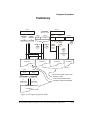
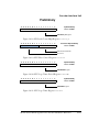
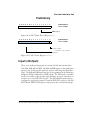
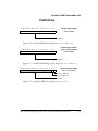
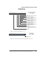
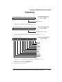
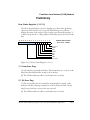
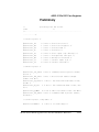
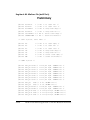
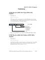
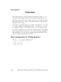
PC Stack Page (STACKP) and
PC Stack Address (STACKA) Registers
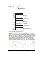
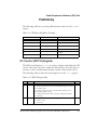
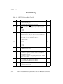
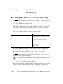
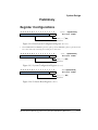
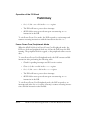
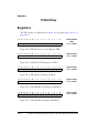
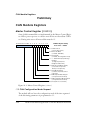
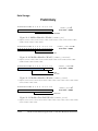
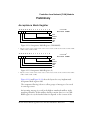
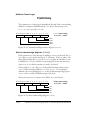
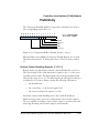
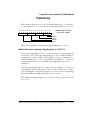
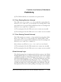
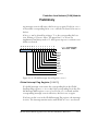
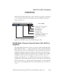
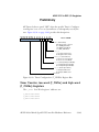
These are non-memory mapped, register group 1 and 3 registers (REG1,
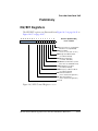
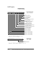
REG3). The PC Stack Page (STACKP) and PC Stack Address (STACKA) registers hold the top entry in the Program Counter (PC) address stack. The
upper 8 bits of the address go into STACKP, and the lower 16 bits go into
STACKA. The PC stack is 33 levels deep.
On JUMP, CALL, DO…UNTIL (loop), and PUSH PC instructions, the DSP
pushes the PC address onto this stack, loading the STACKP and STACKA registers. On RTS/I (return) and POP PC instructions, the DSP pops the
STACKP:STACKA address off of this stack, loading the PC register.
For information on using these registers, see “Stacks and Sequencing” on
page 3-32.
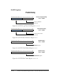
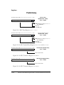
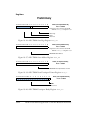
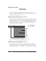
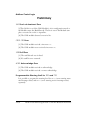
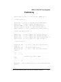
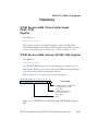
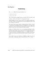
Loop Stack Page (LPSTACKP) and
Loop Stack Address (LPSTACKA) Register
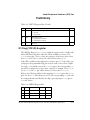
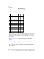
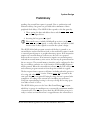
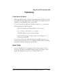
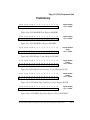
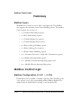
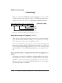
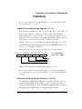
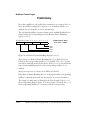
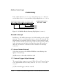
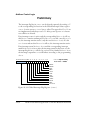
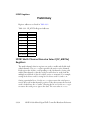
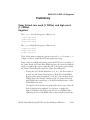
These are non-memory mapped, register group 2 and 3 registers (REG2,
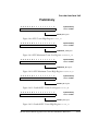
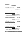
REG3). The Loop Stack Page (LPSTACKP) and Loop Stack Address
(LPSTACKA) registers hold the top entry in the loop stack. The upper 8 bits
of the address go into LPSTACKP, and the lower 16 bits go into LPSTACKA.
The loop stack is 8 levels deep.
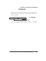
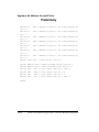
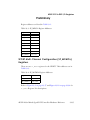
On DO…UNTIL (loop) instructions, the DSP pushes the end of loop address
onto this stack, loading the LPSTACKP and LPSTACKA registers. On
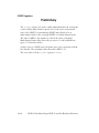
PUSH LOOP instructions, the DSP pushes the (explicitly loaded) contents of
the LPSTACKP and LPSTACKA registers onto this stack.
ADSP-2199x Mixed Signal DSP Controller Hardware Reference
22-17