1
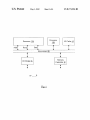
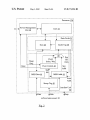
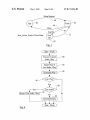
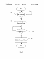
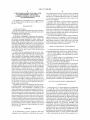
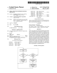
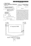
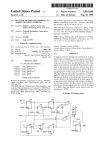
US008171326B2
(12) United States Patent
Keller et al.
(54)
(56)
L1 FLUSH MECHANISM TO FLUSH CACHE
FOR POWER DOWN AND HANDLE
COHERENCE DURING FLUSH AND/OR
AFTER POWER DOWN
U.S. PATENT DOCUMENTS
5,632,038 A
5,784,628 A
5,903,908 A
(US); Tse-Yu Yeh, Cupertino, CA (US);
Ramesh Gunna, San Jose, CA (US);
Brian J. Campbell, Sunnyvale, CA (US)
(73) Assignee: Apple Inc., Cupertino, CA (US)
Notice:
*May 1, 2012
References Cited
(75) Inventors: James B. Keller, Redwood City, CA
(*)
US 8,171,326 B2
(10) Patent N0.:
(45) Date of Patent:
5/1997 Fuller
7/1998 Reneris
5/1999 Singh et al.
6,021,474 A
2/2000 Milling
6,125,450
6,571,333
6,760,819
6,782,472
9/2000
5/2003
7/2004
8/2004
Kardach
Jain et al.
Dhong et al.
Jain et al.
9/2004
Dai ............................. .. 713/320
A
B1
B2
B2
6,792,551 B2 *
6,976,181 B2 * 12/2005 Dai et a1.
7,164,610 B2 *
Subject to any disclaimer, the term of this
patent is extended or adjusted under 35
USC 154(b) by 135 days.
1/2007
713/320
Kimura et al. .............. .. 365/195
7,325,100 B2
1/2008 Dhiman et al.
7,752,474 B2 *
7/2010
Keller et al. ................ .. 713/324
OTHER PUBLICATIONS
This patent is subject to a terminal dis
claimer.
Intel, “Pentium Family User’s Manual,” Chapter 30, “Power Man
agement”, vol. 1: Data Book, ISBN: l-555l2-225-6, 1994, pp. l-ll.
(21) Appl. N0.: 12/7s5,s42
(22) Filed:
* cited by examiner
May 24, 2010
Primary Examiner * Chun Cao
(65)
Prior Publication Data
US 2010/0235670 A1
(74) Attorney, Agent, or Firm * Lawrence J. Merkel;
Meyertons, Hood, Kivlin, KoWert & GoetZel, PC.
Sep. 16, 2010
(57)
Related US. Application Data
(63)
Continuation of application No. 11/525,584, ?led on
Sep. 22, 2006, noW Pat. No. 7,752,474.
(51)
Int. Cl.
(52)
(58)
US. Cl.
G06F 1/32
ABSTRACT
In one embodiment, a processor comprises a data cache con
?gured to store a plurality of cache blocks and a control unit
coupled to the data cache. The control unit is con?gured to
?ush the plurality of cache blocks from the data cache respon
sive to an indication that the processor is to transition to a loW
poWer state in Which one or more clocks for the processor are
(2006.01)
..................................................... .. 713/324
inhibited.
Field of Classi?cation Search ................ .. 713/324,
7 1 3/3 23
20 Claims, 4 Drawing Sheets
See application ?le for complete search history.
I. ____________________ __
Processor 25:
|
<-I->
Power Management
Unit &
i
<—>
I
Core 2
I
I
|
|
1
I
l
I
|
I
l
»
I
:
I
I
I
I
I
I
I
I
I
|
|
|
1
|
l
l
|
l
|
|
I
l
l
l
I
l
1
|
l
|
|
|
|
|
|
|
|
|
|
|
l
|
|
I
I
I
I
I
I
I
Done I
|
I
|
l
|
|
I
I
|
|
|
I
:
:
I ||
I
|
l
I
I
I
I
I
l. ____________________________
I
|
I
MRB Data g
:I II
|
MRB Addr 44
l
\
I
|
I
Snoop Tag Q
I
EvictI I
AddrI I
I I
|
1
Interface Unit I I
:
_________________________________________ _ _ 1
"Data
IIAddr
to/?om Interconnect 20
Resp
US. Patent
May 1, 2012
Processor @
A
Addr RespI
v
Sheet 1 014
US 8,171,326 B2
Processor
L2 Cache E
I
I
l2_B
DataI
Interconnect Q
.
Memory
1/0 Bndge E
Controller E
i
I
US. Patent
May 1, 2012
Sheet 3 014
US 8,171,326 B2
Sleep Request
Start -- Flush
Transmit Current /— 80
Index, Way
I
Signal Done if /— 82
Last Index, Way
I
84
Increment Way
'7
86
Yes
we
Record Last Index, Way
92
No
v
90
Increment Index
End -- Flush
88
N0
US. Patent
May 1, 2012
Sheet 4 M4
US 8,171,326 B2
100
Enter Sleep State?
Yes
V
102 —
Request Core Quiesce,
Assert Sleep Req.
Flush and
Core Done?
104
Yes
r—-—- 106
Inhibit Processor Clocks
US 8,171,326 B2
1
2
L1 FLUSH MECHANISM TO FLUSH CACHE
FOR POWER DOWN AND HANDLE
COHERENCE DURING FLUSH AND/OR
AFTER POWER DOWN
unit coupled to the data cache. The control unit is con?gured
to ?ush the plurality of cache blocks from the data cache
responsive to an indication that the processor is to transition
to a loW poWer state in Which one or more clocks for the
processor are inhibited.
This application is a continuation of US. application Ser.
No. 11/525,584, Which Was ?led on Sep. 22, 2006, now US.
In another embodiment, a system comprises a processor
comprising a data cache con?gured to store a plurality of
cache blocks and a secondary cache coupled to the processor.
Pat. No. 7,752,474.
The processor is con?gured to ?ush the plurality of cache
BACKGROUND
blocks from the data cache responsive to an indication that the
1. Field of the Invention
This invention is related to the ?eld of processors and, more
processor is to transition to a loW poWer state in Which one or
more clocks for the processor are inhibited. The ?ush com
particularly, to handling caches and cache coherency in poWer
prises Writing any modi?ed cache blocks of the plurality of
management modes in processors.
2. Description of the Related Art
As the poWer consumption of processors has increased,
implementation of poWer management modes in processors
cache blocks to the secondary cache.
In yet another embodiment, a method comprises determin
ing that a processor is to transition to a loW poWer state in
Which one or more clocks used by the processor are inhibited;
has become increasing important. In many systems, the
poWer supply is at least sometimes a battery or other stored
charge supply. Maximizing battery life in such systems is
20
often a key selling feature. Additionally, even in systems that
have effectively limitless poWer (e. g. systems plugged into a
Wall outlet), the challenges of cooling the processors and
other circuits in the system may be reduced if the processors
can be placed in loW poWer modes When full processing
cessor is to transition to the loW poWer state.
BRIEF DESCRIPTION OF THE DRAWINGS
25
poWer is not needed.
A variety of poWer management schemes are in use. Typi
cally, the processor may be operated in one of a set of poWer
states. The highest poWer state is the state in Which the pro
cessor executes at its maximum operating frequency, typi
cally supplied by the highest supply voltage used in any of the
and ?ushing a plurality of cache blocks from a data cache
Within the processor responsive to determining that the pro
30
The folloWing detailed description makes reference to the
accompanying draWings, Which are noW brie?y described.
FIG. 1 is a block diagram of one embodiment of a system.
FIG. 2 is a block diagram of one embodiment of a proces
sor shoWn in FIG. 1.
FIG. 3 is a block diagram of one embodiment of a state
machine for ?ushing the data cache shoWn in FIG. 2.
FIG. 4 is a ?owchart illustrating operation in one of the
poWer states. In some cases, other poWer states are de?ned in
Which the processor operates at loWer operating frequencies
and/ or loWer supply voltages (or the loWer frequencies/volt
states shoWn in FIG. 3 for one embodiment.
FIG. 5 is a ?owchart illustrating operation of one embodi
ages may be used Without actually causing a poWer state
transition). Additionally, one or more loWer poWer states are 35 ment of the processor in transitioning to a loW poWer state.
typically de?ned in Which the processor clocks are inhibited
(also referred to as disabled the clocks or “turning off’ the
clocks). Since the processor clocks are not toggling, logic in
the processor does not change state and the poWer consumed
by the processor may be largely reduced. In some loW poWer
40
states, the processor is still supplied With supply voltage to
permit the state of the processor, including any caches, to be
retained even though the clocks are disabled. In other loW
poWer states, the supply voltage may be deactivated as Well
and the processor state is lost. Typically, the processor must
45
DETAILED DESCRIPTION OF EMBODIMENTS
be reset from a loW poWer state in Which the processor’s
supply voltage Was deactivated.
A challenge in processors that implement loW poWer states
in Which the supply voltage is maintained, and thus the caches
retain their state, is the maintenance of coherency in the
System OvervieW
50
caches With respect to any memory transactions that may be
generated by other devices/processors While the processor is
in the loW poWer state. In some cases, systems “Wake up” the
processor to a higher poWer state to perform a snoop (and then
return the processor to the loW poWer state). PoWer is con
sumed in Waking up the processor, often for a snoop that does
not hit in the cache. In other cases, the processor is designed
to continue clocking the cache and a portion of the processor
that interfaces to the cache during the loW poWer states. The
cache and related circuitry is thus in a different clock domain
than the rest of the processor, Which complicates the overall
55
Turning noW to FIG. 1, a block diagram of one embodiment
of a system 10 is shoWn. In the illustrated embodiment, the
system 10 includes processors 12A-12B, a level 2 (L2) cache
14, an I/O bridge 16, a memory controller 18, and an inter
connect 20. The processors 12A-12B, the L2 cache 14, the I/O
bridge 16, and the memory controller 18 are coupled to the
interconnect 20. More particularly, as illustrated With regard
to the processor 12A, the agent coupled to the interconnect 20
may communicate via transactions having address, response,
60
and data phases on the interconnect 20. While the illustrated
embodiment includes tWo processors 12A-12B, other
embodiments of the system 10 may include one processor or
more than tWo processors. Similarly, other embodiments may
include more than one L2 cache 14, more than one I/O bridge
processor design.
SUMMARY
16, and/ or more than one memory controller 18. In one
65
In one embodiment, a processor comprises a data cache
con?gured to store a plurality of cache blocks and a control
While the invention is susceptible to various modi?cations
and alternative forms, speci?c embodiments thereof are
shoWn by Way of example in the draWings and Will herein be
described in detail. It should be understood, hoWever, that the
draWings and detailed description thereto are not intended to
limit the invention to the particular form disclosed, but on the
contrary, the intention is to cover all modi?cations, equiva
lents and alternatives falling Within the spirit and scope of the
present invention as de?ned by the appended claims.
embodiment, the system 10 may be integrated onto a single
integrated circuit chip (eg a system on a chip con?guration).
In other embodiments, the system 10 may comprise tWo or
US 8,171,326 B2
3
4
more integrated circuit components coupled together via a
circuit board. Any level of integration may be implemented in
various embodiments.
In the illustrated embodiment, cache coherent communi
cation is supported on the interconnect 20 via the address,
12A-12B may include circuitry that executes the instructions
de?ned in the instruction set architecture. In one embodi
response, and data phases of transactions on the interconnect
ment, the processors 12A-12B implement the PoWerPCTM
instruction set architecture. HoWever, other embodiments
may implement any instruction set architecture (e. g. MIPSTM,
SPARCTM, x86 (also knoWn as Intel Architecture-32, or
20. Generally, a transaction is initiated by transmitting the
IA-32), IA-64, ARMTM, etc.).
address of the transaction in an address phase, along With a
command indicating Which transaction is being initiated and
The processors 12A-12B may each include a data cache,
and may also be con?gured to enter a loW poWer state in
various other control information. Cache coherent agents on
the interconnect 20 use the response phase to maintain cache
Which one or more clocks used by the processor are inhibited.
When a processor 12A-12B is to transition to the loW poWer
coherency. Each coherent agent responds With an indication
of the state of the cache block addressed by the address, and
cannot be determined or for other reasons. Retried transac
state, the processor 12A-12B may be con?gured to ?ush the
data cache. Flushing the data cache may include Writing any
cache blocks that have been modi?ed by the processor in the
cache (and thus the copy in the memory system and/or the L2
tions are cancelled, and may be reattempted later by the
initiating agent. The order of successful (non-retried) address
processor. Flushing may also include invalidating the cache
phases on the interconnect 20 may establish the order of
transactions for coherency purposes. The data for a transac
blocks in the cache, in some embodiments. In other embodi
ments, the cache block states may be changed to another state,
may also retry transactions for Which a coherent response
tion is transmitted in the data phase. Some transactions may
cache 14, if any, is not the most recent copy) out of the
20
be used solely to establish a change in the coherency state of
a cached block. Generally, the coherency state for a cache
block may de?ne the permissible operations that the caching
agent may perform on the cache block (e.g. reads, Writes,
etc.). Common coherency state schemes include the modi
?ed, exclusive, shared, invalid (MESI) scheme, the MOESI
scheme Which includes an oWned state in addition to the
MESI states, and variations on these schemes. Generally, a
cache block may refer to a contiguous block of data Which is
the unit of allocation and deallocation in the caches Within the
system. The cache blocks may be aligned to cache block
boundaries in the memory system.
In some embodiments, coherency is maintained by the
agents on the interconnect 20 snooping transactions and
25
30
35
checking for cached copies of the transactions.
In other embodiments, coherency may be maintained
through the transmission of explicit probe commands on the
interconnect 20, to Which targeted agents respond based on
their cache state. In either case, the maintenance of coherency
may involve responding to external communication and pos
sibly changing cache state responsive to the external commu
nication. Snooping Will be used as an example beloW, but
state. Furthermore, if the cache blocks are invalidated or
changed to a state that is knoWn externally (eg by the L2
cache 14), the processor 12A-12B need not respond to snoops
(or probes) at all. Accordingly, the clocks to the processor
may be disabled, including the clocks to the data cache and
corresponding snoop circuitry. For example, in one embodi
ment, the processors 12A-12B may implement a duplicate set
of cache tags for coherency purposes (referred to as “snoop
tags”). The snoop tags may be disabled along With the rest of
the processor 12A-12B. Accordingly, the processor 12A-12B
need not have separate clock domains to keep the coherency
maintenance circuitry/ data cache active in the loW poWer
state, in some embodiments, although a processor 12A-12B
may implement multiple clock domains for other reasons.
Furthermore, the processor 12A-12B need not be Woken up
40
from the loW poWer state to respond to a snoop, in some
embodiments.
In some embodiments, the loW poWer state may also
include deactivating the poWer supply. Since the modi?ed
explicit probes may be used in other embodiments.
The interconnect 20 may have any structure. For example,
the interconnect 20 may have separate address, response, and
data interfaces to permit split transactions on the interconnect
20. The interconnect 20 may support separate address and
data arbitration among the agents, permitting data phases of
45
transactions to occur out of order With respect to the corre
50
sponding address phases. Other embodiments may have in
order data phases With respect to the corresponding address
phase. In one implementation, the address phase may com
prise an address packet that includes the address, command,
and other control information. The address packet may be
such as shared, as described in more detail beloW.
Since the modi?ed cache blocks have been Written out of
the processor 12A-12B, the processor 12A-12B need not be
able to supply data for any memory transactions that may
subsequently occur While the processor is in the loW poWer
not include a data phase. For example, some transactions may
cache blocks have been Written back to the L2 cache 14 or
other memory external to the processor 12A-12B, no data is
lo st from the data cache When the poWer supply is deactivated.
The L2 cache 14 may be an external level 2 cache, Where
the data and instruction caches in the processors 12A-12B are
level 1 (L1) caches. In one implementation, the L2 cache 14
may be a victim cache for cache blocks evicted from the L1
caches. The L2 cache 14 may have any construction (e.g.
direct mapped, set associative, etc.).
The modi?ed cache blocks ?ushed from the processors
12A-12B When entering a loW poWer state may be Written to
55
the L2 cache 14, in one embodiment. Accordingly, the latency
to reload the ?ushed blocks into the data cache of the proces
sors 12A-12B after returning to a high poWer state may be the
transmitted in one bus clock cycle, in one embodiment. In one
particular implementation, the address interconnect may
include a centraliZed arbiter/address sWitch to Which each
latency of an L2 cache hit, assuming the blocks remain stored
source agent (e.g. processors 12A-12B, L2 cache 14, and I/O
bridge 16) may transmit address requests. The arbiter/address
sWitch may arbitrate among the requests and drive the request
in the L2 cache 14 at the time the processors 12A-12B Wake
from the arbitration Winner onto the address interconnect. In
one implementation, the data interconnect may comprise a
limited crossbar in Which data bus segments are selectively
coupled to drive the data from data source to data sink.
The processors 12A-12B may comprise circuitry imple
menting an instruction set architecture. That is, the processors
60
up. Additionally, in embodiments that implement the system
10 as a system on a chip, Writing the modi?ed cache blocks to
the L2 cache 14 may consume less poWer than Writing the
blocks to the external (off chip) memory.
65
A loW poWer state may refer to any state that the processor
12A-12B may enter that is designed to consume less poWer
than the normal state of executing at full speed in the proces
sor. Such states may be referred to as sleep states, and the term
5
6
sleep state Will be used as an example herein. Other terms
cache 34 may comprise a plurality of cache block storage
locations, Where each cache block storage location is con?g
used for loW power states include nap, deep sleep, power
doWn, etc.
ured to store a cache block. In the illustrated embodiment,
each cache block storage location comprises a memory loca
tion in the cache tags memory 38 and a memory location in
the data memory 40. The cache tags memory 38 stores a tag
The U0 bridge 16 may be a bridge to various I/O devices or
interfaces (not shown in FIG. 1). Generally, the I/O bridge 16
may be con?gured to receive transactions from the I/O
devices or interfaces and to generate corresponding transac
tions on the interconnect 20. Similarly, the I/O bridge 16 may
locating the corresponding cache block in memory. The tag
may generally include a portion of the address that excludes
the cache offset portion and the portion used to index the data
cache 34, in set associative or direct mapped embodiments.
The cache tags memory 38 may also store the cache coher
receive transactions on the interconnect 20 that are to be
delivered to the I/O devices or interfaces, and may generate
corresponding transactions to the I/O device/interface. In
some embodiments, the I/O bridge 16 may also include direct
ency state (eg MESI state or MOESI state, in some embodi
ments), validity of the cache block, replacement data such as
least recently used (LRU) state, etc. The data memory 40 may
memory access (DMA) functionality.
The memory controller 18 may be con?gured to manage a
main memory system (not shoWn in FIG. 1). The memory in
the main memory system may comprise any desired type of
memory. For example, various types of dynamic random
store the cache block of data. The cache tags memory 38 may
detect a hit or miss in response to a cache access, and may
provide controls to the cache data memory 40 to read/Write
access memory (DRAM) such as synchronous DRAM
(SDRAM), double data rate (DDR) SDRAM, etc. may form
the main memory system. The processors 12A-12B may gen
20
erally fetch instructions from the main memory system, and
sor 12A. That is, the core 32 may include the circuitry that
may operate on data stored in the main memory system. I/O
devices may use the main memory system to communicate
With the processors 12A-12B (eg via DMA operations or
individual read/Write transactions).
Processor
Turning next to FIG. 2, a block diagram of one embodiment
of the processor 12A is shoWn. The processor 12B may be
similar. In the embodiment of FIG. 2, the processor 12A
includes a poWer management unit 30, a core 32, a data cache
34, and an interface unit 36. The poWer management unit 30
is coupled to one or more external signals received by the
processor 12A, and is coupled to the core 32 and the interface
unit 36. The core 32 is coupled to the data cache 34, Which is
coupled to the interface unit 36. The data cache 34 comprises
fetches, decodes, executes, and Writes results of the instruc
25
data to the core 32 (for a read). In the event of a cache miss, a
30
35
unit 36 comprises a ?ush control unit 42, a memory request
buffer (MRB) address buffer 44, an MRB data buffer 46, a
40
45
50
55
detail beloW. The MRB address buffer 44 may subsequently
transmit the snoop address (or the index and Way of the cache
storage location that is hit by the snoop, as determined from
the snoop tag 48). If the snoop hits a dirty (modi?ed) cache
block in the data cache 34, the cache tag memory 38 may
assert the snoop hit dirty signal (Snp Hit Dirty in FIG. 2) to the
60
MRB address buffer 44 and may direct the data memory 40 to
output the modi?ed cache block to the MRB data buffer 46. It
is noted that, While the snoop address input to the data cache
34 (through the mux 50) is illustrated separately from the
vide a snoop hit signal to the ?ush control unit 42 and to the
MRB address buffer 44. The interface unit 36 is further
coupled to receive and provide snoop responses on the
response portion of the interconnect 20.
The data cache 34, in the illustrated embodiment, includes
the cache tag memory 38 and the data memory 40. The data
block stored in the data cache 34 is detected. That is, the snoop
tags 48 may be duplicate cache tags for the cache tag memory
38, used for snooping purposes. If no snoop hit is detected, the
interface unit 3 6 may generate an appropriate response for the
snooped transaction. If a snoop hit is detected, the interface
unit 36 may generate the response and the MRB address
buffer 44 may queue the snoop address (responsive to the
snoop hit signal from the snoop tag 48). The ?ush control unit
42 may also receive the snoop hit signal, as described in more
the MRB address buffer 44 to receive a snoop address, and an
input from the ?ush control unit 42 to receive a ?ush index
and Way. The mux select control is provided by the ?ush
control unit 42. The MRB data buffer 46 is coupled to receive
and provide data from/to the data memory 40 and to receive
and provide data on the data portion of the interconnect 20.
The snoop tag 48 is coupled to receive an address from the
address portion of the interconnect 20, and the MRB address
buffer 44 is coupled to receive and transmit addresses on the
address portion. The snoop tag 48 is further coupled to pro
provide the evict data to the MRB data buffer 46 from the data
memory 40.
For snoop operations from the interconnect 20, the snoop
tag 48 may be checked to determine if a snoop hit on a cache
event of a hit in the data cache 34) to/from the core 32. The
cache tag memory 38 is further coupled to receive snoop
addresses (and ?ush address info) from the mux 50 and to
provide a snoop hit dirty indication and evict address to the
MRB address buffer 44. The mux 50 has an input coupled to
?ll request for the data cache 34 may be queued in the MRB
address buffer 44, and the missing cache block may be ?lled
to the data cache 34. When the missing cache block is ?lled
into the data cache 34, another cache block may be evicted
from the data cache 34. The data cache 34 may provide the
evict address (shoWn as Evict Addr in FIG. 2) to the MRB
address buffer 44. The same path may be used for miss
addresses and for cache blocks being Written back in response
to a snoop, in some embodiments. The data cache 34 may also
unit 42 and to receive a done signal from the ?ush control unit
42. The core 32 is con?gured to transmit memory requests to
the data cache 34 (and more particularly to the cache tag
memory 38). The cache tag memory 38 is coupled to the data
memory 40, Which is coupled to provide/receive data (in the
tions in the instruction set. The core 32 may generate read and
Write cache accesses to the data cache 34 (eg in response to
executing load/ store operations de?ned in the instruction set
architecture). In the event of a cache hit, the data cache 34
may update With data from the core 32 (for a Write) or provide
a cache tag memory 38 and a data memory 40. The interface
snoop tag 48, and a multiplexor (mux) 50. In the illustrated
embodiment, the poWer management unit 30 is con?gured to
transmit a sleep request signal (sleep req.) to the ?ush control
the appropriate data memory location.
The core 32 generally includes the circuitry that imple
ments instruction processing in the processor 12A, according
to the instruction set architecture implemented by the proces
input of the core 32 to the cache tags memory 38, the snoop
and core accesses may share a port on the data cache 34/cache
65
tag memory 38, in some embodiments.
The ?ush control unit 42 may share the path to the data
cache 34 With the snoop address from the MRB address buffer
44, through the mux 50 in the illustrated embodiment. Gen
7
8
erally, the power management unit 30 may detect that a tran
sition to sleep state is desired (eg from external inputs to the
that cause invalidation. The processor 12A may transition to
a higher poWer state if such a snoop occurs. Alternatively, the
power management unit 30, through internal monitoring by
L2 cache 14 or other external circuitry may be con?gured to
the poWer management unit 30, or a combination of external
queue one or more invalidating snoops for presentation to the
input and internal monitoring, in various embodiments). If a
transition to sleep state is desired, the poWer management unit
processor 12A upon transition to the higher poWer state, and
the processor 12A may be transitioned to the higher poWer
state temporarily if the queue ?lls. In yet another alternative,
the L2 cache 14 may be con?gured to tag cache blocks that
Were ?ushed from the data cache 34 but retained in shared
state and may detect snoop invalidations to such cache blocks
30 may communicate With the core 32 to cause the core 32 to
quiesce instruction execution and may also communicate
With the ?ush control unit 42 to indicate that the transition to
sleep state is to occur. For example, in the illustrated embodi
ment, the poWer management unit 30 may assert the sleep
request signal to the ?ush control unit 42.
for queuing or to transition to the processor 12A to a higher
poWer state for servicing the snoop. In still another altema
tive, the L2 cache 14 or other external circuitry may detect a
snoop invalidate (or a snoop hit invalidate) and may cause the
entire data cache 34 to be invalidated When the processor 12A
Responsive to the assertion of the sleep request signal, the
?ush control unit 42 may ?ush the data cache 34 of the cache
blocks stored therein. More particularly, the ?ush control unit
42 may generate a plurality of requests to the data cache 34.
Each request may access a different cache block storage
transitions to a higher poWer state.
location in the data cache 34 and may cause a ?ush of the
cache block stored therein, if any. The data cache 34 may
respond, for cache block storage locations that store modi?ed
20
cache blocks, by asserting the snoop hit dirty signal and
providing the address of the modi?ed cache block as the evict
address to the MRB address buffer 44. The cache block data
may be provided to the MRB data buffer 46 from the data
memory 40 as Well. The data cache 34 may also invalidate the
snooped transaction (or probe). In such an embodiment, the
?ush control unit 42 may receive a snoop received signal
25
instead of the snoop hit signal, and may interrupt ?ushing to
permit the snoop.
The interface unit 36 may further include the circuitry (not
shoWn in FIG. 2) for interfacing betWeen the processor 12A
components and other components coupled to the intercon
30
nect 20, such as the processor 12B, the L2 cache 14, the I/O
bridge 16, and the memory controller 18. While the embodi
cache block in the data cache, updating the cache tag memory
38. Thus, the ?ush requests may operate similar to a snoop
invalidate in the data cache 34 and similar to an evict for the
MRB buffers 44 and 46. Once the data cache 34 has been
?ushed, the ?ush control unit 42 may signal done to the poWer
management unit 30. The poWer management unit 30 may
permit the transition to sleep state responsive to the done
signal assertion and responsive to the core 32 having qui
ment of the interface unit 36 in FIG. 2 implements separate
address and data buffers for the MRB, other embodiments
may implement a combined buffer. Additionally, a separate
esced.
In one embodiment, the data cache 34 has a set associative
35
structure. In such an embodiment, each request generated by
the ?ush control unit 42 may comprise the index and Way of
the cache block storage location to be accessed. In a direct
mapped embodiment, only the index may be included in the
request.
40
During ?ush operation, the ?ush control unit 42 may gen
Way generated by the ?ush control unit 42. If ?ush operation
the data cache 34 (responsive to the snoop hit signal from the
snoop tag 48, in the illustrated embodiment). The ?ush con
trol unit 42 may select the snoop address from the MRB
address buffer 44 for one access (e. g. one clock cycle) in
response to the snoop hit. The selection of the snoop address
may be delayed from the assertion of the snoop hit by one or
more clock cycles to permit the snoop address to be Written to
the MRB address buffer 44 and to be available on the snoop
address input to the mux 50. It is noted that the mux 50 merely
illustrates the path sharing betWeen the ?ush index and Way
and the snoop address. Other embodiments may implement
the path sharing in any desired fashion.
In the present embodiment, ?ushing of the data cache 34
includes Writing modi?ed cache blocks out of the processor
12A (eg to the L2 cache 14) and invalidating the cache
blocks in the data cache 34. Other embodiments may imple
ment ?ushing in other Ways. For example, in one embodi
ment, each valid cache block may be changed to shared state
in the data cache 34. In such an embodiment, the only snoops
that may require service in the data cache 34 may be snoops
snoop address and data buffer may be used, in some embodi
ments. Generally, a buffer such as the MRB may comprise
any memory structure that is logically vieWed as a plurality of
entries. In the case of the MRB, each entry may store the
information for one transaction to be performed on the inter
connect 20 or snooped from the interconnect 20. In some
cases, the memory structure may comprise multiple memory
arrays (eg the address buffer 44 and the data buffer 46).
Additionally, the memory structure may comprise clocked
storage devices such as ?ops, latches, registers, etc. Any
erate the mux select to the mux 50 to select the ?ush index and
is not in progress, the ?ush control unit 42 may select the
snoop address input to the mux 50 from the MRB address
buffer 44. The ?ush control unit 42 may also be con?gured to
interrupt ?ush operation to permit a snoop hit to be serviced in
It is noted that the snoop tag 48 may provide a ?lter for
snoops, determining Which snoops are to be provided to the
data cache 34 for state changes and/or to Write out modi?ed
cache blocks. Other embodiments may not implement the
snoop tag 48, and may snoop the data cache 34 for each
45 combination of one or more memory arrays and/or one or
more clocked storage devices may be used.
50
55
It is noted that, While the illustrated embodiment shoWs the
?ush control unit 42 as part of the interface unit 36, other
embodiments may implement the ?ush control unit 42 as part
of the data cache 34 or betWeen the data cache 34 and the
interface unit 36.
Turning noW to FIG. 3, a block diagram of one embodiment
of a state machine that may be implemented by one embodi
ment of the ?ush control unit 42 is shoWn. In the illustrated
embodiment, the state machine includes an idle state 60, a
?ush state 62, and a snoop hit (snp hit) state 64.
In the idle state 60, no ?ush is in progress. The state
machine remains in the idle state until a sleep request is
indicated by the poWer management unit 30 (arc 66), in Which
60
65
case a transition to the ?ush state 62 occurs. In the ?ush state
62, a ?ush is in progress and the ?ush control unit 42 gener
ates ?ush requests to the data cache 34. The state machine
remains in the ?ush state 62 until either the ?ush is complete
and done is signalled, in Which case a transition to the idle
state 60 occurs (arc 68), or until a snoop hit is signalled to the
?ush control unit 42, in Which case a transition to the snoop hit
state 64 occurs (arc 70). From the snoop hit state 64, a tran
US 8,171,326 B2
10
sition automatically occurs back to the ?ush state 62 (arc 72),
thus creating a one-request window for the snoop hit to be
serviced in the data cache 34.
In the ?ush state 62, the ?ush control unit 42 is generating
?ush requests. In the idle state 60, no ?ush is in progress and
in the snoop hit state 64, the ?ush control unit 42 is stalling to
permit a snoop hit to be serviced. Accordingly, the mux select
for the mux 50 may be generated to select the ?ush input to the
desired by monitoring one or more external signals to the
processor 12A, monitoring internal operation of the proces
sor 12A (e.g. instruction execution in the core 32), or any
combination thereof. If no transition is desired (decision
block 100, “no” leg), the power management unit 30 may
continue monitoring the external signals and/ or the internal
operation.
If a transition is desired (decision block 100, “yes” leg), the
mux 50 if the state machine is in the ?ush state 62 and to select
the snoop hit input to the mux 50 otherwise. This is illustrated
as the Mux_Select_Flush equation in FIG. 3, where the Mux
power management unit 30 may request that the core 32
quiesce (that is, to cease instruction execution in a consistent
state that permits continued execution upon wake up from the
_Select_Flush signal equaling binary one selects the ?ush
input and equaling binary Zero selects the snoop hit input.
sleep state) and may assert the sleep request signal to the ?ush
control unit 42 (block 102). In some embodiments, quiescing
Turning now to FIG. 4, a ?owchart is shown illustrating one
control unit 42 if the state machine is in the ?ush state 62. The
the core 32 and ?ushing the data cache 34 may be performed
in parallel. In other embodiments, the core 32 may ?rst be
quiesced, and then ?ushing of the data cache 34 may be
?owchart of FIG. 4 may be repeated each clock cycle that the
performed.
clock cycle of operation in one embodiment of the ?ush
state machine is in the ?ush state 62. While the blocks are
shown in a particular order in FIG. 4 for ease of understand
ing, any order may be used. Furthermore, blocks may be
The power management unit 30 may wait for the core 32 to
20
be quiesced and for the ?ush to be complete (decision block
104). Responsive to both the core 32 being quiesced and the
performed in parallel in combinatorial logic within the ?ush
?ush being completed (decision block 104, “yes” leg), the
control unit 42. Upon transition from the idle state 60 to the
?ush state 62, the current way and index may be initialiZed to
power management unit 30 may inhibit the processor clocks
Zero in this embodiment.
in other embodiments) (block 106).
The ?ush control unit 42 may transmit the current index
and way as the ?ush index and way to the mux 50 (block 80).
If the current index and way are the last index and way of the
?ush operation, the ?ush control unit 42 may signal done to
the power management unit 30 (and the state machine may
transition to the idle state 60) (block 82). The ?ush control
(or may permit external circuitry to inhibit processor clocks,
25
is fully appreciated. It is intended that the following claims be
30
unit 42 may increment the current way to generate the way for
the next request (block 84). If the current way is the last way
of the set (decision block 86, “yes” leg) and the current index
is not the last index of the indexes to the data cache 34
(decision block 88, “no” leg), the ?ush control unit 42 may
35
40
a control unit coupled to receive an indication that the
processor is to transition to a low power state, wherein
the control unit is coupled to the data cache and is con
coherence operation processing in the data cache,
wherein the coherence operation is used to maintain
cache coherence in the data cache.
that the last index and way are being transmitted so that the
?ush control unit 42 may signal done when transmitting the
last index and way to the data cache 34 (block 92). Alterna
tively, signalling of done may be delayed until the last index
and way have been transmitted and the last modi?ed cache
blocks are in the MRB (or have been written out of the
interpreted to embrace all such variations and modi?cations.
What is claimed is:
1. A processor comprising:
a data cache con?gured to store a plurality of cache blocks;
and
?gured to ?ush the plurality of cache blocks from the
data cache responsive to the indication that the processor
is to transition to the low power state, and wherein the
control unit is con?gured to interrupt the ?ush to permit
increment the current index to generate the index for the next
request (block 90). If the current way is the last way of the set
(decision block 86, “yes” leg) and the current index is the last
index of the indexes to the data cache 34 (decision block 88,
“yes” leg), the ?ush control unit 42 may record an indication
Numerous variations and modi?cations will become
apparent to those skilled in the art once the above disclosure
45
2. The processor as recited in claim 1 wherein the coher
ence operation is a snoop.
3. The processor as recited in claim 1 wherein the coher
ence operation is a probe.
4. The processor as recited in claim 1 wherein the data
cache comprises a cache tag memory con?gured to store a
processor 12A).
The embodiment illustrated in FIG. 4 increments through
the ways of a given index before moving to the next index.
plurality of cache tags corresponding to the plurality of cache
Other embodiments may increment through the possible
50
indexes in a given way before moving to the next way. Still
other embodiments may start with the last index and way and
decrement to Zero. Any mechanism that generates each index
and way or otherwise ?ushes each cache block from the data
cache 34 may be used.
Turning now to FIG. 5, a ?owchart illustrating operation of
one embodiment of the power management unit 30 is shown.
While the blocks are shown in a particular order in FIG. 5 for
ease of understanding, any order may be used. Furthermore,
55
blocks may be performed in parallel in combinatorial logic
60
blocks, and wherein the processor further comprises a second
tag memory dedicated to coherence processing, and wherein
the coherence operation is checked in the second tag memory
for a hit, and wherein the control unit is con?gured to inter
rupt the ?ush to permit the coherence operation processing
responsive to the hit.
5. A system comprising:
a processor comprising a data cache con?gured to store a
plurality of cache blocks; and
within the power management unit 30. Blocks, combinations
a secondary cache coupled to the processor;
wherein the processor is con?gured to ?ush the plurality of
cache blocks from the data cache responsive to an indi
of blocks, and/or the ?owchart as a whole may be pipelined
cation that the processor is to transition to a low power
over multiple clock cycles.
state in which one or more clocks for the processor are
The power management unit 30 may determine whether or
not a transition to the sleep state is desired (decision block
inhibited, and wherein the processor is con?gured to
insert a coherence operation to be processed by the data
cache during the ?ush of the data cache and to interrupt
the ?ush to insert the coherence operation, wherein the
100). As mentioned previously, the power management unit
30 may determine whether or not a transition to sleep state is
65
US 8,171,326 B2
11
12
coherence operation is used to maintain cache coherence
in the data cache, and Wherein the ?ush comprises Writ
ing any modi?ed cache blocks of the plurality of cache
blocks to the secondary cache.
6. The system as recited in claim 5 Wherein the data cache
comprises a cache tag memory con?gured to store a plurality
13. The method as recited in claim 10 Wherein ?ushing the
plurality of cache blocks comprises Writing modi?ed cache
blocks to a memory external to the processor.
14. The method as recited in claim 13 Wherein ?ushing the
plurality of cache blocks further comprises invalidating the
plurality of cache blocks in the data cache.
15. The method as recited in claim 13 Wherein ?ushing the
plurality of cache blocks further comprises changing a state
of the plurality of cache blocks to the shared state.
16. A processor comprising:
of cache tags corresponding to the plurality of cache blocks,
and Wherein the processor further comprises a second tag
memory dedicated to coherence processing, and Wherein
coherence operations received by the processor are ?ltered
through the second tag memory, and Wherein coherence
operations that hit in the second set of tags are processed in
the data cache.
7. The system as recited in claim 5 Wherein the plurality of
cache blocks remain stored in the cache subsequent to the
?ushing.
8. The system as recited in claim 7 Wherein a coherence
state of each of the plurality of cache blocks stored in the
cache at a completion of the ?ush is a shared state.
9. The system as recited in claim 5 further comprising a
poWer management unit con?gured to generate the indica
20
a data cache;
control circuitry con?gured to cause the data cache to Write
any modi?ed cache blocks from the data cache and
further con?gured to cause the data cache to change a
state of any cache blocks in the cache to a shared state,
the control circuitry con?gured to cause the data cache
to Write the modi?ed cache blocks and to change the
state responsive to a poWer management unit request for
the processor to enter a sleep state;
Wherein the processor is con?gured to respond to a snoop
invalidate operation during the sleep state by invalidat
tion.
10. A method comprising:
ing at least one cache block in the data cache subsequent
to Waking up from the sleep state.
detecting that a processor is to enter a loW poWer state;
?ushing a plurality of cache blocks stored in a data cache of
the processor;
during the ?ushing, detecting a snoop operation to be ser
viced by the data cache;
interrupting the ?ushing to service the snoop operation
responsive to detecting the snoop operation; and
resuming the ?ushing subsequent to servicing the snoop
25
more snoop invalidates.
18. The processor as recited in claim 16 Wherein the
Wakeup from the sleep state is to begin processing instruc
30
operation.
11. The method as recited in claim 1 0 Wherein detecting the
snoop operation to be serviced comprises detecting a hit in a
snoop tags memory that is separate from the data cache,
Wherein a miss in the snoop tags for a second snoop operation
indicates that the second snoop operation is not to be serviced
in the data cache.
12. The method as recited in claim 10 further comprising
entering the loW poWer state responsive to completing the
?ushing.
17. The processor as recited in claim 16 Wherein the
Wakeup from the sleep state is temporary to process one or
tions in the processor.
19. The processor as recited in claim 16 Wherein the pro
cessor is con?gured to queue a plurality of snoop invalidate
operations that hit in the cache to be invalidated in response to
the processor Waking up from the sleep state.
35
20. The processor as recited in claim 16 Wherein the pro
cessor is con?gured to cause the data cache to invalidate any
cache blocks stored in the data cache in response to the snoop
invalidate during the sleep state.