1
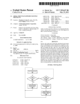
US005815690A
United States Patent [19]
[11]
Patent Number:
Kowert et al.
[45]
Date of Patent:
[54]
5,815,690
Sep. 29, 1998
Iotech Smart Approach to Instrumentation 1993 Catalog,
DEGLITCH METHOD AND APPARATUS TO
ASSURE VALID DATA SAMPLING
National Instruments Corporation, “Analyzer 488, IEEE
Bus Analyzer,” pp. 51—54 and pp. 37—41.
[75] Inventors: Robert C. Kowert, P?ugerville;
1993—1994 ICS Electronics Corporation Catalog, “IEEE
488/GPIB Bus Analyzer With Multiline Display,” pp.
7—1—7—6, 4811 Bus Analyzer With Multiline Display, 6
Andrew Thomson, Austin, both of Tex.
[73] Assignee: National Instruments Corporation,
Austin, Tex.
pages (not numbered).
GPIB—410 User Manual, Mar. 1994 Edition, Part Number
[21] Appl. No.: 916,500
[22] Filed:
Aug. 22, 1997
320053—01, National Instruments Corporation, pp. i—xv,
1—1—4—33, A—1—I—1, and Index 1—Index 12.
Related US. Application Data
[63]
Continuation of Ser. No. 472,967, Jun. 7, 1995, abandoned.
Primary Examiner—Dennis M. Butler
Attorney, Agent, or Firm—Conley, Rose & Tayon; Robert C.
KoWert; Jeffrey C. Hood
[51]
Int. Cl.6 ..
[52]
U.S. Cl. ................ ..
.......................... .. G06F 1/04
[58]
Field of Search ................................... .. 395/551, 552,
. 395/552; 395/555; 364/574
[57]
395/555, 558; 327/379, 380, 381, 392;
A deglitch circuit for ?ltering false transitions of an input
signal based on transitions of a clock signal. A plurality of
memory devices as provided for detecting the input signal
being assay for tWo, three and ?ve transitions of the clock
364/572, 574
[56]
ABSTRACT
References Cited
U.S. PATENT DOCUMENTS
signal in the preferred embodiment. Programmable select
logic is also provided for selecting between these three
cases. In the preferred embodiment, six separate ?ip-?ops
5,014,226
5/1991 Horstmann et al. .
5,018,169
5/1991 Wong et al. .
5,289,060
5,537,379
2/1994 Elnashar et al. .
7/1996 Kimura et al. .
5,649,123
5,649,129
7/1997 Kowert.
7/1997 Kowert.
?ip-?ops being reset upon spurious negations of the input
signal for reign such transitions, and Where tWo of the four
OTHER PUBLICATIONS
?ip-?ops are clocked on the rising edge Whereas the other
tWo are clocked on the falling edge of the clock signal. The
National Instruments Corporation Catalog, TNT4882,
Single—Chip IEEE 488.2 Talker/Listener ASIC, Jun. 10,
programmable select logic preferably includes a multiplexer
are included and clocked by the clocked signal, four of the
for choosing between the three cases. In the preferred
1994, pp. 1—24.
1994 IEEE 488 and VXIbus Control, Data Acquisition, and
Analysis, National Instruments Corporation, “GPIB Moni
embodiment, the input signal is the data valid (DAV) signal
of a GPIB, Where the deglitch circuit assures valid data
sampling on a GPIB.
tor/Analyzer, GPIB—410,” 2—126—2—129, High Performance
Single—Chip GPIB Talker/Listener ASIC, TNT4882, pp.
20 Claims, 10 Drawing Sheets
2—135—2—136.
700 L 1720
\
0
o
/
A
0
724
DAV
722
L0 0-‘L
1
D60
5”
D
U.S. Patent
Sep.29,1998
Sheet 1 0f 10
5,815,690
/102
FIGJ
COMPUTER SYSTEM
MONITOR
II
p \124
/
MAIN
100
130
/
\
MEMORY
122\
126
110
f
GPIB
/
11 0
KEYBOARD __
/
DEVICE 2
BRIDGE
\
LOGIC
GPIB
132
106\
,
DEVICE 1
ANALYZER/
;
/
104
/
CONTROLLER
108
,
‘
;
CARD
GPIB
134
110/
DEVICE 3
GPIB
DEVICE n
/
FIG.2
"0
(PRIOR ART)
DIOI
DIO2
DIO3
DIO5
D106
D107
DIO4
DIO8
EDI
REN
DAv
NRFD
NDAC
IFC
SRO
GND
GND
GND
GND
GND
ATN
SHIELD
,
(TWISTED
(TWISTED
(TWISTED
(TWISTED
(TWISTED
PAIR
PAIR
PAIR
PAIR
PAIR
WITH
WITH
WITH
WITH
WITH
DAv)
NRFD)
NDAC)
IFC)
SRO
GND (TWISTED PAIR WITH ATN
SIGNAL GROUND
U.S. Patent
Sep.29,1998
Sheet 2 0f 10
5,815,690
F763
106
CAD
m4
:02
\
3°°\
cu<
\
4
.._/-- INTERFACE
BUS
—C
,,_N\_..
CHIP
cM
DC
40MHz
—-‘CLK “’
304,‘
DATA
.__ FPGA
“RFD”
;:
NDAC]
306\
GPIB
310/
M
__,
\
DRIVERS
\
\
_
AND
GPIB[15=0]
RECEIVERS
c
‘
W
—
cm
nvr
"*
7
ISA 0R
PCMCIA
308
FIG.4
CA D
GPIB
304
FIFO foo
104
406
402
/
DMA
0R0
BUS
.4»- INTERFACE
|
P’
m__
1.0010
/
400
CD
\
FIFO INTERFACE
_|
LOGIC
"FIFO
INT
\<:>
/410
TIME STAMP
CAPTURE
“Mt-R
LOGIC
——"*'
\408
DATA
00
108
'
r412
0L
-
/404
INTERRUPT
LOGIC
IRQS
FRO“
_ OTHER
T5555’? 4H’
/414
ACCEPTOR
HNSK
BLOCKS
T0 BUS PINS
T0 GPIB PINS
U.S. Patent
Sep.29,1998
Sheet 5 0f 10
5,815,690
><Ql.m
QQ
mNA
mnm
@U8I3Y0
o
mun
mNA
QQQ
I
nNA
mu6E
is @8I3.0
mwkI.-G
J.
5,815,690
1
2
DEGLITCH METHOD AND APPARATUS TO
ASSURE VALID DATA SAMPLING
one device Would be considered a talker and the remaining
devices are listen-only devices. A controller is necessary
When the active or addressed talker or listener must be
changed or recon?gured Where such control functions are
CROSS-REFERENCED TO RELATED
APPLICATIONS
usually handled by a computer device. Also, there may be
multiple controllers on a given GPIB, although only one
controller is the controller-in-charge (CIC) at any given
This application is a continuation of application Ser. No.
08/472,967 ?led on Jun. 7, 1995, noW abandoned.
This patent application relates to US. patent application
Ser. No. 08/473,110, ?led on Jun. 7, 1995, entitled “GPIB
System for Capturing GPIB Signals at a Predetermined Rate
and Upon Transitions of the Data Valid Signal”, noW aban
doned; US. patent application Ser. No. 08/473,200, ?led on
10
Jun. 7, 1995, entitled “GPIB System Including Real-Time
Time-Stamp”, now US. Pat. No. 5,734,876; US. patent
application Ser. No. 08/472,626, ?led on Jun. 7, 1995,
15
time.
A high speed GPIB handshake protocol referred to as the
HS488 is provided to increase the data transfer rate of a
GPIB system. The HS488 protocol modi?es the IEEE-488
source and acceptor handshake fuictions to achieve the high
speed data transfer rates of up to eight MB/s. Any devices
involved in HS488 compliant transfers must be compatible
With the HS488 protocol. HoWever, non-HS488 devices may
also be coupled to a standard GPIB, Where the HS488
entitled “GPIB System With Improved Parallel Poll
devices must use the standard handshake protocol to assure
Response Detection” Which issued Jul. 15, 1997 as US. Pat.
compatibility. According to the HS488 protocol, the data
valid (DAV) signal is asserted and held for a signi?cant
period, but the data signals themselves and an end or identify
(EOI) control signal may only be valid for a short period of
No. 5,649,123; and US. patent application Ser. No. 08/475,
067, ?led on Jun. 7, 1995, entitled “GPIB System Including
20
Controller and Analyzer” Which issued Jul. 15, 1997 as US.
Pat. No. 5,649,129. All of the applications are assigned to
the same assignee.
time, such as approximately 20 ns, relative to the data valid
(DAV) signal.
A GPIB analyZer is used to monitor a GPIB for testing and
FIELD OF THE INVENTION
25
The present invention relates to GPIB instruments, and
more particularly to a deglitch circuit for detecting valid
GPIB-410 by National Instruments Corporation (National
Instruments), Which is used in a similar manner as a logic
transitions of the data valid (DAV) signal.
DESCRIPTION OF THE RELATED ART
30
for a long period of time, When certain events do occur, such
as data transfers according to HS488 protocol, these events
occur very quickly and should be sampled and captured
functions, including laboratory research, process monitoring
35
RS-232 interface protocol, as Well as data acquisition
(DAQ) systems, as knoWn to those skilled in the art. The
present invention generally relates to the GPIB and related
instruments.
The GPIB, otherWise referred to as the Institute of Elec
trical and Electronic Engineers IEEE-488 interface bus, Was
appropriately. Sampling at a ?xed rate, even if at a very fast
rate of 50 nanoseconds (ns), may still miss important events
such as data signal changes Which could potentially occur
or electrical machinery, to name a feW examples. Aplurality
of I/O interface options are available for alloWing commu
nication among various instrumentation systems, including
the GPIB (general purpose interface bus), the VXI bus, the
analyZer to monitor the control and data signals of the GPIB.
Prior art GPIB analyZers usually sample data from the GPIB
at a ?xed rate. Although activity may not occur on a GPIB
Scientists and engineers often use laboratory and indus
trial instrumentation systems to perform a variety of
and control, data logging, analytical chemistry, tests and
analysis of physical phenomena and control of mechanical
debugging purposes, Where the analyZer captures data from
the GPIB for display and analysis. One such example is the
betWeen 50 ns samples. This is particularly true on a GPIB
also including HS488 compliant devices, Where data trans
40
fers occur very quickly When compared to standard GPIB
data transfer protocols. For example, 50 ns samples Would
detect changes of the DAV signal, but could potentially miss
changes of the data and E01 signals since these signals
45
remain valid for only a very short time period.
Most prior art GPIB analyZers connect to a GPIB system
as a separate GPIB device. Thus, if a GPIB system contains
the normal limit of 14 devices, a device Would have to be
removed to add a prior art GPIB analyZer to the GPIB
designed for remote control of programmable instruments.
Thousands of measurement instruments from hundreds of
suppliers are available With a GPIB interface. GPIB instru
ments are typically more sophisticated and have higher
system. Also, prior art GPIB analyZers are either stand-alone
products containing a poWer supply and vieWing screen, or
performance than other interface options, including DAQ
an expansion or circuit card designed to plug into a standard
and RS-232 boards. Aplurality of instruments, usually up to
14, are coupled through a GPIB using eight-bit parallel
computer I/O bus, such as the industry standard architecture
(ISA) bus. The prior art GPIB analyZer circuit card type
protocol to achieve data transfer rates of over one megabyte
per second (MB/s). The GPIB devices can be listeners,
talkers and/or controllers. A talker sends data messages to
55
further requires an additional I/ O slot to any GPIB controller
card Which may be installed in the same computer.
It is further noted that it is often desired to determine the
one or more listeners, Which receive the data The controller
actual or “real” time that particular information or data Was
manages the How of information on the GPIB by sending
commands to all devices. Some devices may perform sev
captured from the GPIB. Logic analyZers, for example, often
attach a time-stamp value to a particular piece of data
eral functions, such as a digital voltmeter Which acts as a 60 captured from a group of signals or a bus. The logic analyZer
talker by sending voltage information on the GPIB and as a
includes a simple counter that may rollover or time-out
listener When receiving con?guration and control informa
several times, so that the time-stamp value does not indicate
tion. Usually, there is only one controller for a given GPIB
Where multiple GPIB devices are further coupled to the
GPIB for receiving command information from the control
ler for interfacing the other GPIB devices. It is noted that
some GPIB con?gurations do not require a controller if only
rollovers occur. A real-time time-stamp requires a signi?
cantly large number of counters to indicate elapsed time With
a desired degree of accuracy and time increment resolution.
real time betWeen capture events if one or more of such
65
OtherWise, the counter circuitry rolls over and the user may
5,815,690
3
4
not be aware of such rollover. This leads to inaccurate or
exhibit false transitions. Aunique data valid deglitch circuit
detects such glitches of the DAV signal and thereby sepa
otherwise misleading results.
Prior art GPIB controllers and/or analyzers may obtain the
rates valid from invalid DAV transitions. This assures that
status of multiple devices using the parallel poll conmand.
valid data is captured into the buffer. The deglitch circuit is
Up to eight different devices can be con?gured to respond to
preferably programmable for ?ltering false transitions of the
the parallel poll command by assigning one of the eight
DAV signal based on a clock signal. The deglitch circuit
preferably includes a ?rst memory circuit for detecting the
DAV signal remaining asserted for at least tWo consecutive
GPIB data lines to each device. When the command is
issued, each device asserts its assigned data line to indicate
that the device is present on the GPMB and requesting
service. The GPIB data byte is then retrieved for determin
transitions of a clock signal and a second memory circuit for
10
ing the status of the con?gured devices, Where each data
signal represents a one bit status. Prior art GPIB analyZers
often yield inaccurate results because of the Way the data is
sampled during parallel polling. The response of the devices
may be delayed and there is no de?ned hold time for a device
15
to hold its response valid. Some prior art analyZers retrieve
data at a ?xed rate, so that the data could be retrieved before
all of the devices have had a chance to respond or after one
or more of the devices have responded and have already
negated their responses by the time the data is sampled,
thereby resulting in invalid or missed responses. Some
devices update their poll status bit during the parallel poll
command, thus such updates may be missed by a ?xed rate
sampling device.
Some analyZers retrieve data both at the beginning and
end of the parallel poll command. HoWever, valid responses
occurring during the command may still be missed. Still
other analyZers sample only at the end of the parallel poll
25
conditions. Each of the memory circuits preferably com
prises a set of ?ip-?ops.
A time-stamp timer may be enabled to provide a real-time
time-stamp value for each set of data captured into the
buffer. If enabled, the capture logic asserts a time-stamp
select signal to the select logic and enables the buffer for
inserting the time-stamp value into the buffer after each
capture. In this manner, all of the important transitions
occurring on the GPIB are captered into the FIFO along With
a real-time time-stamp value identifyng When each capture
occurred.
The timer includes a counter Which provides a relative
resets the counter after each capture. In the preferred
embodiment, the timer is a 16-bit counter incremented every
50 ns, Which does not rollover until after approximately 3.28
milliseconds
Upon such rollover, the counter asserts a
improved performance for capturing all important events
time-out signal to the capture logic, Which correspondingly
occurring on a GPIB as Well as for time-stamping the
35
enables the maximum timer value of FFFFh (a loWer-case
“h” indicating hexadecimal) to be Written into the buffer.
The FIFO is preferably a 2K by 18 bit buffer including tWo
extra bits for each 16-bit data value. One of the extra bits is
SUMMARY OF THE INVENTION
A GPIB system according to the present invention
includes a GPIB controller and a GPIB analyZer on the same
circuit card. The combined controller and analyZer functions
require a single connection to the GPIB and a single I/O slot
in a host computer.
transitions of the clock circuit The user can program the
memory circuit to select betWeen any one of these three
elapsed time betWeen captures, Where the capture logic
command, thus valid responses or updated responses may be
completely missed. It is desired to handle all of these cases
and retrieve valid and updated responses.
In sum, it is desired to provide a GPIB analyZer With
captured events in real-time. It is also desired to provide a
GPIB analyZer that does not require additional computer or
GPIB resources to those required by an existing GPIB
controller.
detecting the DAV signal remaining asserted for three con
secutive clock transitions. A programmable memory circuit
selects betWeen the ?rst and second memory circuits. Also,
the deglitch circuit can include further memory circuitry for
detecting the DAV signal asserted for ?ve consecutive
45
The GPIB system includes sampling logic for sampling
the GPIB synchronously or at a predetermined rate, as Well
as for sampling the GPIB asynchronously, or according to
preferably set for the ?rst rollover or time-out value, thereby
marking the ?rst time the timer times out. An interrupt is
generated When this buffer location is read to alert the
softWare to count remaining time-out values in order to
compute the total elapsed time betWeen true data values
captured from the GPIB. The softWare easily calculates the
real time betWeen each of the true capture data values by
summing any time-out values multiplied by 3.28 ms, as Well
as by multiplying other time-stamp values by 50 ns.
In this manner, a real-time timer marks all signi?cant
events on the GPIB With a relatively high resolution, Which
changes of the DAV signal. This technique alloWs data to be
captured at a regular interval as Well as on edge transitions
is preferably achieved using a single 16-bit counter clocked
of the DAV signal. The synchronous logic samples data once
every 50 ns. For edge transition capturing, the DAV signal
every 50 ns. It is noted that since time-out occurs only once
every 3.28 ms during long periods of inactivity, the softWare
is easily able to keep up With the FIFO, thereby preventing
itself is used as the sampling event to clock a set of ?ip-?ops
to assure that valid data is not missed by the synchronous
logic. Data valid logic detects valid transitions of the DAV
signal and provides a data transition select signal to select
logic, Which sWitches betWeen the synchronous GPIB
over?oW of the FIFO. In an alternative embodiment, each
55
time-stamp value captured into the FIFO is compared With
samples are provided to and stored in a buffer, such as a ?rst
the maximum value (FFFFh) so that the marking and
interrupt method need not be used. This embodiment is
preferred for certain applications Which have a signi?cant
amount of overhead associated With interrupts. In either
in, ?rst out (FIFO) buffer. Capture logic monitors the
sampled GPIB signals and the data transition select signal
calculated and provided to the user.
samples and the asynchronous GPIB samples. The selected
and enables the buffer to capture the selected sample upon
predetermined capture conditions. In this manner, the cor
rect data is detected and captured into the buffer even during
fast data transitions.
Sampling data from the GPIB based on the DAV signal
could result in erroneous data since the DAV signal tends to
embodiment, elapsed time betWeen capture events is easily
A GPIB system according to the present invention
retrieves all valid and updated responses to a parallel poll
command. The GPIB data is captured immediately after a
65
parallel poll command is issued as Well as after the com
mand is deasserted. Also, a timing device causes another
sample to be captured after approximately 2 microseconds
5,815,690
5
6
(,us) to give the devices time to provide a valid response.
Furthermore, more samples are captured during any data line
transitions that occur While the plel poll command remains
asserted. This assures that any initial and updated responses
are captured during the command, Which Would otherWise
be missed in prior art embodiments.
Therefore, a GPIB system according to the present inven
tion captures important events occurring on the GPIB into a
input/output (I/O) or expansion bus 104 Which is preferably
based on the industry standard architecture (ISA) also
referred to as the AT bus. It is noted that the computer 102
may be any one of several knoWn types such as the Apple
Computer or Macintosh or may include any one of several
Work stations such as the Sun SPARCstation, etc. The
buffer in an accurate manner. Also, a timer provides a
real-time time-stamp value, Which is inserted into the buffer
folloWing each associated captured value if desired. The
real-time time-stamp has a high resolution and provides an
accurate temporal determination of each captured value.
Furthermore, both controller and analyZer functions are
included for conserving computer resources.
10
expansion bus 104 could alternatively be based on the
Extended ISA (EISA), the PCMCIA standard or the PCI
(peripheral component interconnect) bus or any one of the
knoWn I/O or expansion buses of computer systems.
A GPIB analyZer/controller card 106 plugs into one of the
I/O slots of the computer 102 for connecting to the expan
sion bus 104 of the computer 102. The GPIB analyZer/
controller card 106 couples the computer 102 to a GPIB 108,
A better understanding of the present invention can be
also knoWn as the IEEE 488 interface bus. At least one and
normally a plurality of GPIB devices 110 are further con
nected to the GPIB 108 in any one of several knoWn
methods, such as series or star con?gurations, etc. Each of
the GPIB devices 110 may be any one of thousands of
obtained When the folloWing detailed description of the
preferred embodiment is considered in conjunction With the
manner, the computer 102, through the GPIB analyZer/
15
BRIEF DESCRIPTION OF THE DRAWINGS
adapted for commnunicating on the GPIB 108. In this
folloWing draWings, in Which:
controller card 106, controls all of the GPIB devices 110 on
the GPIB 108. Each of the GPIB devices 110 can be
listeners, talkers and/or controllers as knoWn to those skilled
FIG. 1 is a simpli?ed block diagram illustrating a GPMB
system including a GPIB analyZer according to the present
invention;
25
FIG. 2 is a diagram illustrating the standard GPIB signals;
FIG. 3 is a simpli?ed block diagram of a GPIB system
according to the present invention including analyZer and
controller functions;
FIG. 4 is a simpli?ed block diagram of the GPIB analyZer
portion of the GPIB system of FIG. 3;
FIG. 5 is a schematic diagram illustrating the logic for
capturing GPIB control signals;
FIG. 6A is a schematic diagram illustrating logic for
capturing the data signals of the GPIB;
FIG. 6B is a schematic diagram illustrating logic for
capturing the end or identify control signal of the GPIB;
35
The computer 102 may include bridge logic 120, for
coupling the expansion bus 104 to a system (or local) bus
122, although other con?gurations are contemplated. The
computer 102 further includes a microprocessor 124, such as
an 80386, i486 or Pentium processor by Intel, and main
memory 126 coupled to the system bus 122. Of course, the
computer 102 also typically includes a monitor 130 and
FIG. 7A is a schematic diagram of the logic for identify
ing the assertion of the DAV signal of the GPIB;
associated graphics controller (not shoWn) as Well as input
devices such as a keyboard 132 and mouse 134. In this
manner, the user loads softWare routines into main memory
FIG. 7B is a schematic diagram of the deglitch circuit of
FIG. 7A;
FIGS. 7C and 7D are timing diagrams illustrating opera
tion of the deglitch circuit of FIGS. 7A and 7B;
in the art. In the preferred embodiment, the GPIB analyZ
erlcontroller card 106 includes the primary controller of the
GPIB 108 for controlling each of the GPIB devices 110. As
Will be described more fully beloW, the GPIB analyZer/
controller card 106 further includes the GPIB analyZer for
monitoring signals on the GPIB 108 for testing and debug
ging purposes by capturing data or control signals from the
GPIB 108 for display and analysis.
126 (from data drives, etc.) for execution by the micropro
cessor 124 for sending and receiving data and commands for
45
FIG. 8 is a schematic diagram of the time-stamp timer of
programming and controlling the GPIB analyZer/controller
card 106, and for ultimately controlling or otherWise moni
toring the GPIB 108 and associated GPIB devices 110.
FIG. 4;
FIG. 9 is a schematic diagram illustrating logic for
Referring noW to FIG. 2, a diagram is shoWn of a GPIB
connector With standard signal assignment as knoWn to
those skilled in the arts Pin numbers 1—4 and 13—16 com
performing parallel poll;
FIGS. 10A and 10B are simpli?ed logic diagrams illus
trating logic for identifying predetermined capture condi
prise the eight-bit data bus of the GPIB 108, including data
tions of the control and data signals, respectively;
FIG. 11 is a schematic diagram of the logic for identifying
bus signals D101—D108, otherWise referred to as the DIO
all capture conditions on the GPIB;
FIGS. 12A and 12B illustrate a capture logic state
signals. The connector 200 includes three handshake signals
for asynchronously controlling the transfer of message bytes
55
betWeen the GPIB devices 110 for guaranteeing that data is
sent and received Without transmission error. The handshake
machine and its operation; and
FIG. 13 is a schematic diagram of the multiplexer logic
lines include a not ready for data (NRFD) signal Which
for capturing data into a FIFO buffer.
message byte. The NRFD signal is driven by any device
indicates When a device is ready or not ready to receive a
receiving commands, by listeners When receiving data
DETAILED DESCRIPTION OF THE
PREFERRED EMBODIMENT
messages, and by a talker When enabling the HS488 mode.
A not data accepted (NDAC) signal indicates When a device
has or has not accepted a message byte. The NDAC signal
is driven by any of the GPIB devices 110 When receiving
Referring noW to FIG. 1, a simpli?ed block diagram is
shoWn of a GPIB system 100 including a GPIB analyZer and
controller card 106 implemented according to the present
invention. A computer 102, Which is preferably a personal
computer (PC) such as the XI or AT by IBM, includes an
65
commands and by listeners When receiving data messages.
A data valid (DAV) signal indicates When the DIO signals
are stable and valid and thus can be accepted safely by any
5,815,690
7
8
of the GPIB devices 110. The GPIB analyZer/controller card
106 drives the DAV signal When sending commands, and a
talker drives the DAV signal When sending data messages.
The GPIB 108 further includes ?ve interface management
signals for managing the How of information across the
Referring noW to FIG. 4, a block diagram is shoWn of the
FPGA 304 coupled to the eXpansion bus 104, to the GPIB
108, and to the FIFO 300. Bus interface logic 400. decodes
register accesses to the other functional blocks Within the
FPGA 304 and couples to the DMA logic 402 and the
GPIB 108. An attention (ATN) signal is driven by the GPIB
analyZer/controller card 106 When using the DIO data sig
interrupt logic 404 to generate DMA and interrupt requests.
The DMA logic 402 is connected to a FIFO interface 406 in
order to detect When data is present in the FIFO 300 so that
DMA may be requested to unload data from the FIFO 300.
nals to send commands, and otherWise drives the ATN signal
loW to alloW a talker to send data messages. An interface
clear (IFC) signal is driven by a controller to initialiZe the
The FIFO interface 406 provides the control signals to read
GPIB 108 and to establish that controller as the controller
data from or Write data to the FIFO 300.
in-charge (CIC). A remote enable (REN) signal is driven by
The primary function of the FPGA 304 is to capture the
state of the control and data signals of the GPIB 108 based
on certain programmed conditions. The control and data
signals of the GPIB 108 are all sampled every 50 ns by
capture logic 410. Also the DIO and EOI signals are sampled
upon assertion edge transitions of the DAV signal. This
the controller to place the devices in remote or local program
mode. A service request (SRQ) signal is driven by any one
of the GPIB devices 110 to asynchronously request service
from the GPIB analyZer/controller card 106. Finally, an end
or identify (EOI) signal is used by a talker to mark the end
of a message string and is alternatively used by the controller
15
asynchronous sample of the DIO and EOI signals is desired
because they might otherWise be missed at the 50 ns ?Xed if
HS488 transfers are used. If a programed capture condition
to tell the GPIB devices 110 to identify their response in a
parallel poll command.
Referring noW to FIG. 3, a block diagram is shoWn of the
is true, the sample retrieved by the capture logic 410 is
GPIB analyZer/controller card 106 implemented according
provided through the FIFO interface 406 to the FIFO 300. If
the capture condition is not true, the sample retrieved from
the GPIB 108 is discarded. A capture enable signal referred
to the present invention. The eXpansion bus 104 includes
control (C), address (A), and data (D) signals connected to
the primary controller portion referred to as the TNT 308,
Which is preferably the TNT4882C ASIC by National Instru
to as CAPiEN determines Whether capturing is enabled or
25
ments but may be any GPIB controller circuit such as the
NEC 7210. The TNT 308 is further connected to the data (D)
and control (C) signals of the GPIB 108. The TNT 308
preferably performs the basic IEEE 488 talker, listener, and
control functions required by the ANSI/IEEE 488.2 standard
(ANSI is the American National Standard Institute). In the
preferred embodiment using the ISA expansion bus, the
handshake line transitions by monitoring state changes of
the NDAC, NRFD and DAV signals; upon control line
trnitions by monitoring the IFC, REN, ATN and SRO signals
TNT 308 preferably can sustain data transfers up to 1.5
MB/s using the IEEE 488.1 standard three-Wire handshake.
The TNT 308 also preferably implements the high speed
35
an ISA platform or 3.4 MB/s on a computer system incor
porating the EISAplatform. It is noted that for embodiments
using different expansion buses, the TNT data transfer rates
800 (FIG. 8) preferably clocked by the CLK50 signal for a
may vary. The TNT 308 is also used to monitor the GPIB
108 as Well as to provide device emulation, source
resolution of 50 ns per bit. Of course, other frequencies and
resolutions are contemplated and are a matter of design
choice. The tinier 408 is used to determine the amount of
time betWeen capture events of the GPIB 108 through the
handshaking, and pattern generation.
Preferably, a bus interface chip 310 provides a chip select
to the TNT 308 and to the primary analyZer portion, referred
capture logic 410. Thus, Whenever time-starting is enabled,
45
Semiconductor that conforms to the ISA Plug and Play
speci?cation is used. The bus interface chip 310 preferably
interfaces DMA (direct memory access) channels and inter
rupt request signals (IRQ) to the eXpansion bus 104. The
FPGA 304 controls the capturing of the status of the GPIB
108 into a high speed 2K by 18 bit FIFO 300. Through the
FPGA 304, the GPIB analyZer/controller card 106 can be
con?gured to capture and/or trigger on any transition or state
of interest on the GPIB 108. The captured status is then read
for any state changes; upon command tranfer When both the
ATN and DAV signals are true; upon data transfer When
ATN is false and DAV is true; upon data line tranitions; upon
time-stamp timer rollover of a time-stamp timer 408; and
When a Force Capture Pulse Command is through softWare.
The time-stamp timer 408 includes a 16-bit counter circuit
GPIB protocol (HS488) for data transfers up to 1.6 MB/s on
to as the FPGA 304. In the preferred embodiment, a bus
interface chip such as the NM95MS15P from National
disabled. If the CAPiEN signal is true and the FIFO 300 is
not full, capturing Will take place according to one of several
capture conditions as folloWs: When a trigger condition is
true; upon the occurrence of a parallel poll When a signal
IDY is true, Where IDY=ATN & EOI (FIG. 9); upon
55
from the FIFO 300 by the computer system 102 for analysis
and display on the monitor 130, if desired. An oscillator 302
provides a 40 MHZ clock signal (CLK) to the FIFO 300, the
FPGA 304, and the TNT 308. The CLK signal is used to
develop tWo clock signals internal to the FPGA 304, one
a time-stamp value is Written into the neXt location of the
FIFO 300 after a sample is captured into the FIFO 300 from
the capture logic 410, as described more ?lly beloW. In this
manner, the FIFO 300 contains GPIB samples and time
stamp values in alternating locations.
Trigger logic 412 coupled to the GPIB 108, the bus
interface logic 400 and the capture logic 410 alloWs the
FPGA 304 to trigger on any predetermined pattern of signals
appearing on the GPIB 108. The trigger pattern is speci?ed
and con?gured by a trigger and pattern register (TRPR) and
a trigger mask register (TRMR). Setting a bit in the TRMR
register indicates that trigger logic 412 Will treat the corre
sponding signal on the GPIB 108 as a don’t care. For each
bit that is not set Within the TRMR register, the trigger state
of the signals of GPIB 108 are determined by the state of the
corresponding TRPR register bits. Thus, a trigger condition
having a 25 ns period referred to as CLK25 and another
having a 50 ns period referred to as CLK50. Also, GPIB
occurs When a sample of the GPIB 108 equals the pattern
drivers and receivers 306 provide interfacing of the FPGA
turing is enabled and if triggering bits are set, the current
GPIB sample is captured into the FIFO 300 each time the
trigger condition tranitions from false to true or alternatively,
only the ?rst time the trigger condition tranitions from false
304 to the GPIB 108, Where the GPIB drivers and receivers
306 are used by the FPGA 304 to independently assert the
control signals of the GPIB 108 for the acceptor handshake
and to receive the signals of the GPIB 108 for capturing.
speci?ed by the TRMR and TRPR registers. Thus, if cap
65
to true.
5,815,690
9
10
Finally, the FPGA 304 is con?gured to participate in the
signals of the GPIB 108 are sampled at 50 ns intervals in a
similar manner as the control signals of the GPIB 108
GPIB handshake as an acceptor through acceptor handshake
logic 414. Participation in the handshake is enabled by
setting an HNSKiEN enable bit in a handshake con?gu
described above in FIG. 5, except that a single signal
CAPiDAT identi?es any changes of state of the DIO data
ration register. Also, the acceptor handshake logic 414 may
signals.
be programmed to vary the rate of the GPIB acceptor
handshake.
Referring noW to FIG. 5, a schematic diagram is shoWn of
The DIO(0) signals are also provided to the respective D
inputs of a set of eight D-type ?ip-?ops 606, each receiving
the DAV signal at their respective clock inputs. In this
the logic for sampling and comparing the control signals of
manner, each of the DIO signals appearing on the GPIB 108
are sampled With each assertion of the DAV signal by the
the GPIB 108. In particular, all of the control signals except
the EOI and DAV signals, including the IFC, REN, SRQ,
ATN, NRFD and NDAC signals, are collectively referred to
10
?ip-?ops 606, Which provide signals DAViDIO(1) at their
respective Q outputs. The DAViDIO(1) signals are pro
as GPIBiCTL(0) as appearing at a time t=0 relative to the
CLK50 signal on the GPIB 108. The GPIBiCTL(t) desig
nation represents individual signals IFC(t), REN(t), SRQ(t),
15
vided to the respective D inputs of a set of eight D-type
?ip-?ops 608 receiving the CLK50 clock signal at their
respective clock inputs. The ?ip-?ops 608 provide a set of
ATN(t), etc. The EOI signal is handled in a similar manner
as the DIO signals, as described beloW. The DAV signal is
handled in a different Way Which is described beloW. The
signals DAViDIO(2) signals at their Q outputs. In this
manner, the DIO(t) signals generally represent samples of
GPIBiCTL(0) signals are each provided to the D inputs of
a set of six D-type ?ip-?ops, collectively referred to by the
reference number 500. Only one ?ip-?op 500 is shoWn, it
being understood that it is repeated six times for each of the
Whereas the DAViDIO(t) signals represent the data signals
control signals of the GPIB 108. It is noted that any
appropriate type of latch or ?ip-?op may be used to sample
signals of the GPIB 108, Where D-type ?ip-?ops are used in
the illustrated embodiment. The CLK50 signal is provided to
are captured by the ?ip?ops 606.
the data signals on the GPIB 108 at a ?xed interval of 50 ns,
of the GPIB 108 When the DAV signal is asserted. In this
manner, very fast changes of the DIO data signals, Which
might otherWise be missed by a ?xed rate capture of 50 ns
Refering noW to FIG. 6B, a schematic diagram is shoWn
25
108, Which is similar to the logic for capturing the DIO data
signals. The EOI signal is provided to the D inputs of tWo
D-type ?ip-?ops 610 and 616. The ?ip-?op 610 receives the
CLK50 signal at its clock input and provides a itched EOI(1)
signal at its Q output. The EOI(1) signal is provided to
another D ?ip-?op 612, Which is also clocked by the CLK50
signal for providing a signal EOI(2) at its Q output The
the clock input of the ?ip-?ops 500 for sampling the control
signals of the GPIB 108 every 50 ns, Where the initial
sampled versions are referred to as signals GPIBiCTL(l) at
the outputs of the ?ip-?ops 500. This process is repeated
again Where the GPIBiCTL(l) signals are provided to the D
inputs of another set of six D-type ?ip-?ops 502, Which
receive the CLK50 signal at their clock inputs. The ?ip-?ops
502 provide signals GPIBiCTL(2) at their Q outputs,
representing latched versions of the GPIBiCTL(l) signals
EOI(1) and EOI(2) signals are provided to the respective
tWo inputs of a tWo-input XOR gate 614, Which provides a
35
after 50 ns.
Each of the GPIBiCTL(2) signals are provided to one
signal CAPiEOI at its output indicating changes of the EOI
signal. The ?ip-?op 616 is clocked by the DAV signal for
sampling the EOI signal upon assertions of the DAV signal,
Where this sampled value is provided as a signal DAYiEOI
input of a set of six, tWo-input exclusive-OR (XOR) gates
504, Where the GPIBCTL(1) signals are provided to the
(1) at the Q output of the ?ip-?op 616. The DAViEOI(1)
signal is provided to the D input of another D ?ip-?op 618,
Which is clocked by the CLK50 signal for providing a signal
DAViEOI(2) at its Q output In this manner, changes of the
EOI signal are sampled along With the DIO signals upon
other input of each of the XOR gates 504. In this manner, the
XOR gates 504 provide a set of CAPiCTLN signals rep
resenting change of state of the control signals of the GPIB
108 betWeen successive clock cycles of the CLK50 clock
signal, for detecting certain capture conditions as described
beloW. The subscript “n” represents multiple signals, Where
CAPiCTL, generally represents all of the signals CAPi
IFC, CAPiREN, CAPiSQR, CAPiATN, CAPiRFD and
CAPiDAC denoting changes of the IFC, REN, SQR, ATN,
NRFD and NDAC signals, respectively.
illustrating logic for capturing the EOI signal of the GPIB
assertion transitions of the DAV signal.
45
Referring noW to FIG. 7A, a schematic diagram is shoWn
illustrating the logic for detecting transitions of the DAV
signal on the GPIB 108. The DAV signal is provided to a
deglitch circuit 700, Which provides a signal SDAV at its
output. It is noted that spurious assertions of the DAV signal
Referring noW to FIG. 6A, a schematic diagram is shoWn
could cause erroneous collection of data Which is not desired
for sampling and detecting changes of the DIO signals on the
by the user. Such erroneous data may be sampled by the
?ip-?ops 606, but are not captured as described before. The
GPIB 108. The DIO signals, collectively referred to as
DIO(0), are provided to the D inputs of a set of eight D-type
?ip-?ops 600, receiving the CLKSO signal at their respective
clock inputs. The Q outputs of the ?ip-?ops 600 provide
deglitch circuit 700 generally detects the spurious assertions
of the DAV signal providing a ?ltered version as the SDAV
55
signal. The SDAV signal is provided to the D input of a
D-type ?ip-?op 704, receiving the CLK25 clock signal at its
clock-input, Where the SDAV signal and the Q output of the
signals DIO(1), Which are latched versions of the DIO(0)
signals. The DIO(1) signals are provided to the D inputs of
another set of eight D-type ?ip-?ops 602, each receiving the
CLK50 signal at their respective clock inputs. The Q outputs
?ip-?op 704 are both provided to the tWo inputs of an OR
gate 706 for providing its output to the binary 0 input of a
of the ?ip-?ops 602 provide latched signals DIO(2) Which
multiplexer (mux) 708. The DAV signal is also provided to
are each provided to one input of a set of eight tWo-input
the binary 1 input of the mux 708, Which receives an
override signal OS at its select input The output of the mux
708 re?ects the selected binary input based on the state of
the select signal provided to the mux 708.
A signal DGO is provided to the non-inverted input of a
tWo input AND gate 718, Which asserts the OS signal at its
XOR gates 604. The DIO(1) signals are provided to the other
respective inputs of the XOR gates 604, Which provide a set
of eight CAP-DATE signals to the respective inputs of an
eight input OR gate 605, Which asserts a signal CAPiDAT
at its output. Thus, the CAPiDAT signal is asserted When
any of the DIO signals change state. In this manner, the data
65
output Another signal DGI is provided to the inverting input
5,815,690
11
12
of the AND gate 718. As described below, the DGO and DG1
signals set timing parameters Within the deglitch circuit 700.
The OS signal is asserted When deglitching is turned off and
the deglitch circuit 700 is effectively bypassed. The output
TABLE 1
Programming values for the DAV Deglitch Circuit
of the mux 708 is provided to the D input of a D-type
?ip-?op 710, receiving the CLK50 signal at its clock input.
DG1, DGO
The Q output of the ?ip-?op 710, referred to as a signal
00
12.5
SDAV1, is provided to the D input of a D-type ?ip-?op 712
receiving the CLK50 signal at its clock input. The Q output
of the ?ip-?op 712 is a signal SDAV2, Which is provided to
the inverting input of a tWo-input AND gate 714, Which
receives the SDAV1 signal at its non-inverting input and
Which provides the CAPiDAViASSRT signal at its output.
The SDAV1 signal is provided to the inverted input of
another tWo-input AND gate 716, Which receives the
SDAV2 signal at its non-inverting input for providing the
01
not used — OS asserted
1O
11
Max Pulse Rejected (ns)
25
5O
Min Pulse Recognized (ns)
25
not used — OS asserted
37.5
75
10
15
CAPiDAViUNASRT signal.
Operation of the circuit shoWn in FIG. 7A is noW
described. It is noted that the DAV signal valid transitions
are normally held long enough for capture by a 50 ns ?xed
rate sampling period. HoWever, it is desired not to capture
sampled data in the event the DAV signal transition Was
spurious and not associated With a valid data change. Any
Where the maximum pulse rejected indicates that the deg
litch circuit 700 Will reject any pulse less than the indicated
duration and the minimum pulse recogniZed indicates that
the deglitch circuit 700 is guaranteed to recogniZe a pulse
greater than the indicated duration. For clarity, the output
signals of the ?ip-?ops 720,726, 724, 722, 730 and 732 are
shoWn as signals A, B, C, D, E and F, respectively, although
signals E and F are referred to as tWo separate signals, E0,
E1 and F0, F1, respectively, in timing diagrams (FIGS. 7C,
7D) depending upon the state of the DGO signal.
The general operation of the deglitch circuit 700 is noW
described. The maximum rejected and minimum recogniZed
pulse times are based on transitions of the CLK25 signal.
valid assertions of the DAV signal on the GPIB 108 as
For the DG1, 0=00 case, a DAV pulse must remain asserted
detected by the deglitch circuit 700 are asserted as the SDAV 25 during at least tWo consecutive transitions of the CLK25
signal for at least 25 ns. The OR gate 706 detects any
signal, Which means for more than 12.5 ns, to be detected by
assertions or deassertions of the DAV signal. When OS is
the ?ip-?op 740. Pulses less than to 12.5 ns do not meet this
loW, such assertions or deassertions are captured by the
?ip-?op 710, Which are provided to the ?ip-?op 712 and also
to the AND gate 714. Thus, the output of the AND gate 714
asserts the CAPiDAViASSRT signal When the DAV sig
nal is asserted from loW to high during any 50 ns clock cycle.
Deassertions or negations of the DAV signal are detected by
criterion and are rejected. It is noted that pulses exactly
equal to 12.5, 25, 37.5 ns etc. having edges concurrent With
the CLK25 transitions may or may not meet the tiring
parameters and are a matter of probability. Such exact cases
are considered trivial and Will be ignored for purposes of this
disclosure. For the DGI, 0=00 case, the A signal is asserted
the AND gate 716 as the CAPiDAViUNASRT signal in a
similar manner.
by the ?ip-?op 720 Whenever the DAV signal is true on a
35
rising edge of the CLK25 signal, but is only asserted While
Referring noW to FIG. 7B, a schematic diagram is shoWn
DAV is true. If DAV is true for at least 12.5 ns, then the
of the deglitch circuit 700. The DAV signal is provided to the
?ip-?op 724 asserts the C signal. Since the ?ip-?op 724
remains asserted for a full clock cycle, the ?ip-?op 740
asynchronous clear inputs of four D-type ?ip-?ops 720, 722,
726 and 730. The ?ip-?ops 720, 722, 726 and 730 receive
the CLK25 signal at their clock inputs, although the ?ip
?ops 722 and 726 invert the CLK25 signal and thus are
clocked on the falling edges. The D inputs of ?ip-?ops 720,
722 are ?xed at a high logic level. The Q output of ?ip-?op
720 is provided to the D input of ?ip-?op 726, to the D input
of another ?ip-?op 724 and to the binary 1 input bit of a
tWo-input mux 727. The ?ip-?op 724 receives the CLK25
signal at its inverted clock input The Q output of ?ip-?op
722 is to the binary 0 input of the mux 728, Which receives
the DGO signal at its select input. The output of mux 728 is
provided to the D input of the ?ip-?op 730, Which provides
its output to the D input of another ?ip-?op 732 receiving the
CLK25 signal at its inverted clock input The Q output of the
?ip-?op 732 is provided to one input of a tWo-input OR gate
734, Which receives the Q output of the ?ip-?op 726. The
output of the OR gate 734 is provided to the binary 10 input
detects Whether the DAV signal is asserted on a rising edge
and lasts at least until the folloWing falling edge of the
CLK25 signal. The ?ip-?op 722 asserts the D signal When
DAV is true on a falling edge of the CLK25 signal, but only
for so long as DAV remains true. If DAV remains true for at
45
encompass tWo consecutive transitions of CLK25 are
detected.
In a similar manner, a DAV pulse must remain asserted for
three consecutive transitions of the CLK25 signal (25 ns) to
be detected When DG1, 0=10. In this case, the B signal is
asserted if the DAV pulse is true on a rising edge and lasts
55
of a three-input mux 738, Which receives the DG1, DGO
signals at its tWo select inputs and provides its output to the
at least until the folloWing falling edge. HoWever, the
?ip-?op 740 only detects the assertion of the B signal if the
DAV pulse remains asserted until the folloWing rising edge,
D input of a D-type ?ip-?op 740. The ?ip-?op 740 receives
the CLK25 signal at its clock input and provides the SDAV
signal at its output. The Q outputs of the ?ip-?ops 722, 724
are provided to the respective inputs of a tWo-input OR gate
736, Which provides its output to the binary 00 input of the
since otherWise the ?ip-?op 726 is cleared Also, the F signal
is asserted by the ?ip-?op 732 only if the DAV pulse is true
on a falling edge as detected by the ?ip-?op 722, and if the
pulse remains true until the next falling edge, since other
Wise the ?ip-?ops 722 and 730 are cleared. Thus, the DAV
pulse must be true for three consecutive transitions of the
mux 738. The Q output of the ?ip-?op 730 is connected to
the binary 11 input of the mux 738.
The deglitch circuit 700 is programmed using the DGO
and DG1 signals to provide recognition according to the
folloWing table 1:
least 12.5 ns until the folloWing rising edge of the CLK25
signal, then the ?ip-?op 740 detects this pulse. In this
manner, any pulse greater than 25 ns is guaranteed to be
detected by the ?ip-?op 740, pulses less than 12.5 ns Will
alWays be rejected and those betWeen 12.5 and 25 ns that
65
CLK25 signal. Thus, pulses greater than 37.5 ns are alWays
detected While pulses less than 25 ns are alWays rejected.
Pulses betWeen 25 and 37.5 ns are only detected as long as
they encompass three consecutive CLK25 transitions.
5,815,690
14
13
one input of the AND gate 804 for starting the counter circuit
For the DG1, 0=11 case, a DAV pulse must remain
asserted for three consecutive rising edges of the CLK 25
800 if enabled and not in a reset state. The CAPiEN signal
signal (50 ns). The ?rst and second rising edges are detected
by the ?ip-?ops 720 and 730, respectively, Which are cleared
unless the pulse remains asserted until the following rising
edge of the CLK25, Where the E signal is latched by the
is provided to the inverted reset input of the ?ip-?op 802 for
keeping the counter circuit 800 in the reset state if the
CAPiEN signal is deasserted When capture is not enabled.
The AND gate 804 receives the TSiEN signal, Which is
asserted to enable time-stamping. The AND gate 804 also
?ip-?op 740. Thus, pulses equal to or less than 50 ns are
alWays rejected While pulses greater than 75 ns are alWays
detected. Again, any pulses having a duration betWeen 50
and 75 ns are detected as long as they remain asserted during
10
three consecutive rising edges.
Referring noW to FIG. 7C and 7D, timing diagrams are
shoWn illustrating operation of the deglitch circuit 700. In
FIG. 7C, the CLK25 signal is provided at the top and ten
pulses are shoWn asserted on the DAV signal, Where pulses
1 and 2 have durations greater than 6 but less than 12.5 ns,
pulses 3 and 4 have durations greater than 12.5 but less than
25 ns, pulses 5 and 6 have durations greater than 25 but less
than 37.5 ns, pulses 7 and 8 have durations greater than 37.5
but less than 50 ns and Where pulses 9 and 10 have durations
greater than 50 ns. For purposes of illustration, pulses 3, 5,
15
T[15z0]. The time signals T[15z0] are preferably separated
into tWo 8-bit portions, Where the T[1518] signals are
referred to as the TIMiHI byte and the T[7:0] signals are
referred to as the TIMiLO byte (FIG. 13).
S The counter circuit 800 asserts a time-out signal TO
indicating rollover. The TO signal could be asserted When
7 and 10 have slightly longer durations than corresponding
respective pulses 4, 6, 8 and 9. The output of the muX 738
is shoWn based on the DGO and DG1 signals. In FIG. 7D, the
CLK25 and DAV signals are repeated and the SDAV signal
is shoWn based on the DGO and DG1 signals for cases 11,
receives a signal RSTiTIM*, Which is asserted loW to reset
the counter circuit 800, as Will be described more fully
beloW. In this manner, the counter circuit 800 remains in a
reset state any time capturing or the time-stamp functions
are disabled, or any time the RSTiTIM’F signal is asserted,
indicating the desire to reset the counter circuit 800.
OtherWise, the counter circuit 800 counts up from 0, pro
viding a 16-bit time value at its outputs as the signals
the counter circuit 800 reaches its maximum value of
FFFFh, Where the T[15z0] signals are all 1’s. In the preferred
25
10 and 00, respectively.
Inspection of FIG. 7D reveals that pulses 1 and 2, being
less than 12.5 ns, are not detected and thus are rejected in all
three cases of the DG1, 0 signals. Pulses 3 and 4 are betWeen
embodiment, hoWever, the counter circuit 800 counts up to
the value FFFDh and asserts the TO signal at FFFDh, Which
occurs tWo CLK50 cycles before it reaches its maXimum
value of FFFFh Upon the neXt CLK50 cycle, the counter
circuit goes to FFFEh and negates the TO signal and tWo
?ip-?ops 1106 and 1108 (FIG. 11) are clocked to assert the
corresponding signals NiCAP and CAP. If the NiCAP
signal is asserted When the counter circuit 800 reaches
FFFEh indicating a normal capture condition has occurred,
it stops counting at FFFEh so that the value FFFEh is Written
12.5 and 25 ns, yet only pulse 3 is detected for the DG1,
0=00 case since pulse 3 encompasses tWo consecutive
transitions of the CLK25 signal While pulse 4 does not. Both
pulses 3 and 4 are rejected by the DG 1, 0=10 and 11 cases.
into the FIFO 300 as a normal time-stamp value. This
Pulses 5 and 6 are both betWeen 25 and 37.5 ns and thus are 35 distinguishes a normal capture from a rollover condition
detected for the DG 1, 0=00 case and yet rejected for the
occurring Without a capture. HoWever, if the NiCAP signal
DG1, 0=11 case. Since pulse 5 encompasses three consecu
detected by both DG1, 0=00, 10 cases, yet rejected by the
is not asserted at FFFEh, the counter circuit 800 provides the
maXimum value FFFFh at its output, Which is then Written
to the FIFO 300 indicating a rollover condition rather than
a normal time-stamp value.
Time-stamping preferably does not start until the ?rst
DG1, 0=11 case. Finally, pulses 9 and 10 are betWeen 50 and
75 ns and detected by both DG1, 0=00, 10 cases, but only
pulse 10 is detected by the DG1, 0=11 case since it encom
TIM* signal ensures the counter circuit 800 is held in the
reset state until after the ?rst capture and is reset upon each
tive CLK25 transitions While pulse 6 does not, pulse 5 is
accepted and pulse 6 is rejected for the DGI, 0=10 case.
Pulses 7 and 8 are both betWeen 37.5 and 50 ns and thus are
passes three consecutive CLK25 rising edges, While pulse 9
capture after time-stamping has been enabled. The RSTi
45
capture. Thus, the time-stamp for the ?rst capture is pref
does not. Although not shoWn, any pulses greater than 75 ns
erably Zero. Since the counter circuit 800 is reset after each
are detected by all three cases.
capture, each time-stamp value represents the elapsed time
Referring noW to FIG. 8, a schematic diagram of the
since the previous capture. HoWever, if a capture or trigger
time-stamp timer 408 is shoWn. The time-stamp timer 408
condition is not met, the counter circuit 800 reaches its
maXimum value of FFFFh in approximately 3.28 ms. In the
includes a 16-bit counter circuit 800, preferably including a
16-bit up-counter, Which receives the CLK50 clock signal at
a clock input. The counter circuit 800 receives a signal
NiCAP, Which is asserted When any capture conditions are
true eXcept rollover of the counter circuit 800. The counter
circuit 800 includes an inverted reset input receiving a signal
preferred embodiment, if the current time-stamp is referred
to as X, and the number of time-outs or rollovers since the
last capture value is y, then the real time value RT in ns is
calculated by the folloWing equation (1):
55
TIMERiRST’E Which is asserted by a three input AND gate
804. An asterisk
RT(ns)=50(x+1)+3,276,750(y)
at the end of a signal name denotes
negative logic, Where the signal is considered asserted When
loW and negated When high. Thus, the counter circuit 800 is
identify capture conditions according to parallel poll
cleared When TIMERiRST’F is asserted loW, so that the
counter circuit 800 goes to Zero and begins counting up
again When TIMERiRST’F is negated.
AD-type ?ip-?op 802 has its D input pulled high to logic
one and receives a CAP signal at its clock input The CAP
signal, described furter beloW, is asserted When any of
several capture conditions are true including rollover of the
timer 800. The ?ip-?op 802 asserts a signal STRTiTIM to
(1)
Referring noW to FIG. 9, a logic diagram is shoWn for
65
responses on the GPIB 108. The EOI(1) and ATN(1) signals
are each provided to the inputs of a tWo-input AND gate 900.
The EOI(2) and ATN(2) signals are each provided to the
inputs of another tWo-input AND gate 902. The outputs of
the AND gates 900, 902 are provided to the respective inputs
of a tWo-input XOR gate 904. The output of the AND gate
900 is also provided to the active loW reset inputs of a timer
906 and a D-type ?ip-?op 908. The timer 906 is preferably
5,815,690
15
16
a 2 microsecond (us) timer including a simple up-counter
clocked by the CLK50 signal. Thus, after 2 us, the timer 906
provides a time-out signal, POLLiTO, Which is asserted
When has elapsed since the reset input of the timer 906 Was
deasserted. The POLLiTO signal is provided to the D input
receives a capture control line transition signal CPiCTL at
of the ?ip-?op 908, having its clock input receiving the
CLK50 signal. The Q output of the ?ip-?op 908 provides a
input OR gate 1004, Which receives the CAPiDAVi
UNASRT signal at its third input. The output of the OR gate
signal POLLiTO, Which is provided to the inverting input
of a tWo-input AND gate 910. The other, non-inverting input
Which receives a capture handshake line transition enable
of the AND gate 910 receives the POLLiTO signal. The
output of the AND gate 910 is provided to one input of a
tWo-input OR gate 912, Which receives the output of the
XOR gate 904 at its other input. The output of the OR gate
912 provides the CAPiIDY signal, Which indicates appro
priate capture conditions according to parallel responses on
its other input. The CPiCTL signal is set in a capture setting
register (CPSR) for enabling detection of any changes of the
IFC, REN, ATN and SRO signals. The CAPiDAC and
CAPiRFD signals are provided to tWo inputs of a three
1004 is provided to one input of a tWo-input AND gate 1006,
10
The CAPiIDY signal is provided to one input of a
tWo-input AND gate 1008, Which receives a capture on
parallel poll response enable signal CPiPPR, Which is set in
15
the GPIB 108.
The CPiPPR and QPOLLiTO signals are provided to
the respective inputs of a tWo-input AND gate 1010, pro
viding its output to one input of a tWo-input OR gate 1012,
CLKSO signal, both EOI(1) and ATN(1) are asserted thereby
removing the reset condition to the timer 906 and the
?ip-?op 908. Also, since the command Was not issued in the
Which receives a capture data enable signal CPiDAT at its
other input The CPiDAT bit is set in the CPSR register. The
output of the OR gate 1012 is provided to one input of a
prior CLK50 cycle, the EOI(2) and ATN(2) signals are not
both asserted so that the XOR gate 904 and the OR gate 912
25
IDY signal. As Will be described more fully beloW, assertion
signal is asserted.
Certain trigger capture conditions are indicated by signals
CAPiSTRIG, CPiTRIG, TMRKiEN and CAPiFRSTi
be captured Upon the neXt CLKSO cycle, the XOR gate 904
deasserts its output loW so that the OR gate 912 deasserts the
CAPiIDY signal. The XOR gate 904 keeps its output loW
until the parallel poll command is deasserted.
TRIG, Where these signals Will not be further described. The
CPiTRIG signal is provided to one input of a tWo-input OR
After 2 us, the timer 906 asserts the POLLiTO signal
gate 1016 receiving the TMRKiEN signal at its other input
35
The output of the OR gate 1016 is provided to one input of
a tWo-input AND gate 1017, receiving the CAPiSTRIG at
its other input. The output of the AND gates 1002, 1006,
1008, 1014 and 1017 as Well as the CAPiFRSTiTRIG
signal are all provided to the respective inputs of a siX-input
OR gate 1018, Which asserts a signal GiCAP When any of
the capture conditions of the AND/ OR logic described above
signal. The QPOLLiTO signal remains asserted until par
allel poll command is deasserted. As described further
beloW, sampled data is captured When the QPOLLiTO
signal is asserted and While the CAPiDAT signal is
asserted, Where the assertion of CAPiDAT indicates a
change of any one of the DIO signals as described previ
tWo-input AND gate 1014, Which receives the CAPiDAT
signal at its other input. Thus, if the CPiPPR bit is set and
the QPOLLiTO signal is asserted, or if the CPiDAT bit is
set, the GPIB signals are captured Whenever the CAPiDAT
of the CAPiIDY signal causes a sample of the GPIB 108 to
While the QPOLLiTO signal is still negated, so that the
AND gate 910 asserts its output causing the OR gate 912 to
assert the CAPiIDY signal once again. Thus, another
sample of the GPIB 108 signals are captured after the GPIB
devices 110 have had 2 us to respond. The ?ip-?op 908 is
then clocked by CLK50 so that the QPOLLiTO signal is
asserted, so that the OR gate 912 deasserts the CAPiDY
the CPSR register. Thus, if the CPiPPR bit is set in the
CPSR register, assertion of the CAPiIDY signal causes a
capture of GPIB samples.
Operation of the parallel poll circuitry of FIG. 9 is noW
described. When a parallel poll command is issued, the EOI
and ATN signals are both asserted. After a rising edge of the
both assert their outputs high, thereby asserting the CAPi
signal CPiHS at its other input, Which is set in the CPSR
register.
is detected and enabled.
FIG. 10B is a logic diagram for identifying certain capture
conditions for capturing the DIO data and EOI signals. A
signal CAPiDAViASSRT, developed by logic described
45
ously. Thus, While the parallel poll command remains
in FIG. 7A and generally representing assertions of the DAV
signal, is provided to one input of a tWo-input AND gate
1020 having its other inverted input receiving the CAPi
AIN(2). The output of the AND gate 1020 provides a signal
asserted, any updated responses by the GPIB devices 110 are
captured. Finally, When the parallel poll command is
deasserted, the XOR gate 904 once again asserts its output
causing the OR gate to assert the CAPiDY signal, causing
CAPiDAB representing a data byte transfer on the GPIB
one last capture of the DIO data signals at the end of the
are also provided to both non-inverting inputs of a tWo-input
AND gate 1022, Which asserts a signal CAPiCOM repre
108. The CAPiDAViASSRT and CAPiATN(2) signals
parallel poll command.
It is appreciated that at least three captures occur during
a parallel poll command, a ?rst upon assertion of the
command, a second capture after 2 us, and a third When the
senting a command transfer on the GPIB 108.
55
parallel poll command is deasserted. Further, more samples
are captured anytime the DIO signals change state indicating
an updated response to the parallel poll command. Thus, a
GPIB system according to the present invention captures all
and a capture command enable signal CPiCOM are pro
vided to the tWo inputs of a tWo-input AND gate 1028, Which
provides its output to a second input of the OR gate 1034.
The CAPiDAB signal is provided to one input of a tWo
possible responses and updated responses to the parallel poll
command.
Referring noW to FIG. 10A, a logic diagram is shoWn for
identifying certain predetermined capture conditions of the
GPIB 108. The CAPiIFC, CAPiREN, CAPiATN and
CAPiSRQ signals are each provided to the four inputs of a
four-input OR gate 1000. The output of OR gate 1000 is
provided to one input of a tWo-input AND gate 1002, which
The CAPiDAViASSRT signal and a capture handshake
line transition signal CPiHS are provided to the tWo inputs
of tWo-input AND gate 1026 Which provides its output to
one input of a three-input OR gate 1034. The CAPiCOM
65
input AND gate 1030, Which receives a capture data byte
enable signal CPiDAB at its other input. The output of the
AND gate 1030 is provided to the third input of the OR gate
1034. The CPiCOM, CPiDAB and CPiHS enable signals
are preferably set in the CPSR register for enabling these
particular capture conditions. The output of the OR gate
5,815,690
17
18
1034 asserts a signal DiCAP, Which is asserted When any
In this manner, sampled signals from the GPIB 108 that
of the enabled capture conditions detected by the AND gate
1026, 1028, 1030 and 1032 are asserted.
meet the capture conditions are Written into the FIFO 300 as
Referring noW to FIG. 11, a schematic diagram is shoWn
of a circuit for detecting any of the capture conditions. The
is enabled, the capture state machine 1200 inserts a time
stamp value from the counter circuit 800 into the neXt
GiCAP, DiCAP and FRCiCAP signals are provided to
the three inputs of a three-input OR gate 1100. The output of
OR gate 1100 is provided to one input of a tWo-input OR
gate 1102 and also to the D input of a D-type ?ip-?op 1106.
The TO signal from the counter circuit 800 is provided to the
other input of the OR gate 1102, Which has its output
provided to the D input of another D-type ?ip-?op 1108. The
CLK50 signal is provided to the clock inputs of both
f?p-?ops 1106, 1108. The CAPiEN signal is provided to an
inverting input of a tWo-input OR gate 1104 and a signal
RESET is provided to the other non-inverting input of the
OR gate 1104. The RESET signal is asserted upon any reset
conditions of the GPIB analyZer/controller card 106. The
output of the OR gate 1104 is provided to the clear inputs of
indicated by the CAP signal being asserted. If time-stamping
location of the FIFO 300 folloWing the capture value, and
the counter circuit 800 is reset If another capture condition
10
is met before the neXt rising edge of the CLK25 signal,
another sampled value is Written into the FIFO 300 folloWed
by another time-stamp value. It is noted that since sampling
primarily occurs at 50 ns intervals and thus at a 20 MHZ rate,
that insertion of the time-stamp value is easily achieved
since the capture state machine 1200 is clocked by the
CLK25 signal at a 40 MH rate. Also, the DIO signals
15
sampled asynchronously With assertion of the DAV signal
are captured “synchronously” With the capture state machine
1200 folloWed by a time-svalue. It is noted that the asyn
chronous samples have higher priority and are selected over
synchronous samples if occurring in the same 50 ns period.
both ?ip-?ops 1106, 1108. The Q output of the ?ip-?op 1106
provides the normal capture signal NiCAP, Which is
Since time-out of the counter circuit 800 is also a “capture”
condition, a dummy GPIB sample is Written into the FIFO
300 folloWed by the maXimum time-stamp value of FFFFh.
asserted When capturing is enabled and any time the prede
Referring noW to FIG. 13, a schematic diagram is shoWn
termined or programmed capture conditions occur, as indi
is asserted upon the same capture conditions as for the
of select logic 1300, Which is preferably located Within the
capture logic block 410, for providing selected data to the
FIFO 300. The GPIBiCTL(2) signals, Where the SDAV2
normal NiCAP signal, and also any time time-out of the
signal as shoWn in FIG. 7A is considered one of the
counter circuit 800 occurs as indicated by the TO signal.
Referring noW to FIG. 12A, a block diagram is shoWn of
GPIBiCTL(2) signals, are provided to 7 of 16 bits of the
binary 10 input of a 3-input, 16-bit muX 1302. The remain
a capture state machine 1200 for detecting and asserting
capture conditions. The capture state machine 1200 receives
ing 9 bits of the binary 10 input receive the EOI(2) and the
DIO(2) signals. The 16 bits of the binary 11 input of the muX
1302 receives the GPIBiCTL(2), the DAViEOI(2) and the
cated by the GiCAP, DiCAP and FRCiCAP signals. The
Q output of the ?ip-?op 1108 asserts the CAP signal, Which
25
the RESET, CAP and TSiEN signals at respective inputs,
and also receives the CLK25 clock signal at its clock input.
The capture state machine 1200 provides tWo signals DAT,
FWEN and the RSTiTIM’F signal at its three outputs As
Will be described more fully beloW, the DAT signal is
asserted by the capture state machine 1200 any time it is
desired to capture sampled signals of the GPIB 108. The
FWEN signal is a FIFO Write enable signal provided to the
FIFO 300 When the sampled value is to be Written into the
FIFO 300. As described previously, the capture state
machine 1200 asserts the RSTiTIM’F signal loW to reset the
DAV DIO(2) signals. The TIMiHI and TlMEiLO bytes
35
selects betWeen GPIB signals and the time-stamp value, and
the DiCAP signal selects betWeen “synchronous” signals,
or GPIB signals latched using the CLK50 signal, and
“asynchronous” signals, or GPIB signals latched by the
DAV signal. It is noted that the asynchronous signals include
counter circuit 800.
the CAPiCOM and CAPiDAB cases as Well as cases With
FIG. 12B is a state machine diagram illustrating operation
of the capture state machine 1200. A ?rst state 1202 is
entered upon reset conditions When the RESET signal is
45
or time-stamp values from the counter circuit 800, are
captured into the FIFO 300 When the FWEN signal is
machine 1200 enters a state 1204 upon the neXt assertion of
55
signal remains negated. If the time-stamp function is
disabled, as indicated by a TSiEN signal being negated,
CLK25 signal for purposes of synchroniZation. The marker
condition by the state of the NiCAP and CAP signals. In
particular, if the NiCAP signal is not asserted and the CAP
signal is asserted, then a rollover condition has occurred.
The marker circuit 1310 also includes memory for deter
neXt assertion of the CLK25 signal. If TSiEN is asserted,
the state machine 1200 enters state 1206 upon the neXt
assertion of the CLK25 signal. In state 1206, the FWEN,
RSTiTIM’F and DAT signals are all asserted. Upon the neXt
assertion of the CLK25 signal, if CAP is asserted, the state
machine 1200 reenters state 1204 to Write another group of
data into the FIFO 302. OtherWise, the state machine 1200
clock signal.
asserted.
The NiCAP, CAP and DAT signals are provided to a
timer rollover marker circuit 1310, Which also receives the
circuit 1310 determines Whether a capture is due to rollover
of the counter circuit 800 as opposed to a normal capture
then the state machine 1200 reenters state 1202 upon the
reenters state 1202 upon the neXt assertion of the CLK25
assertions of the DAV signal, With reference to FIG. 1OB.
The 16 output bits of the muX 1302 are provided to the D
inputs of a set of 16 D-type ?ip-?ops 1304, receiving the
CLK25 signal at their clock inputs. The Q outputs of the
?ip-?ops 1304 are provided to 16 inputs of the FIFO 300.
The FIFO 300 receives the FWEN signal at its enable input
Thus, sampled data and control signals from the GPIB 108,
asserted by the GPIB controller/analy=card 106. In state
1202, the DAT signal is asserted and the FWEN and
RSTiTIM’F signals are negated, Where negation is indicated
by a bar above the signal name in the Figures. Upon
assertion of the CAP signal, indicating any of the data or
control capture conditions described previously, the state
the CLK25 clock signal. The FWEN signal is asserted in
state 1204 and the DAT signal is negated. The RSTiTIM’F
are provided to the 16 bits of the binary OX input of the muX
1302, Where “X” indicates a binary 0 or 1 (don’t care). The
?rst select input of the muX 1302 is the DAT signal and the
second is the DiCAP signal. In this manner, the DAT signal
65
mining if the prior capture Was due to rollover or a normal
capture condition for identifying a ?rst rollover from sub
sequent consecutive rollovers. If a rollover occurs and the
previous capture Was a regular capture, so that the rollover
is the ?rst rollover, the marker circuit asserts a signal MARK