1
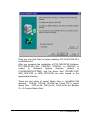
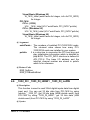
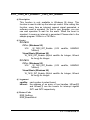
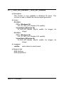
PCI-7432 / 7433 / 7434 cPCI-7432 / 7433 / 7434 64 Channels Isolated Digital I/O / Digital Input / Digital Output Card @Copyright 1998~1999 ADLink Technology Co., Ltd. All Rights Reserved. Manual Rev. 2.10: November 28, 1998 The information in this document is subject to change without prior notice in order to improve reliability, design and function and does not represent a commitment on the part of the manufacturer. In no event will the manufacturer be liable for direct, indirect, special, incidental, or consequential damages arising out of the use or inability to use the product or documentation, even if advised of the possibility of such damages. This document contains proprietary information protected by copyright. All rights are reserved. No part of this manual may be reproduced by any mechanical, electronic, or other means in any form without prior written permission of the manufacturer. Trademarks NuDAQ, NuIPC, PCI-7432, PCI-7433, PCI-7434, cPCI-7432, cPCI-7433, cPCI-7434 are registered trademarks of ADLink Technology Co., Ltd. Other product names mentioned herein are used for identification purposes only and may be trademarks and/or registered trademarks of their respective companies. Getting service from ADLink Tech. Inc. Customer satisfaction is always the most important thing for ADLink Tech. You can get more information and our service from several channels below. 1. Visit our web site: http://www.adlink.com.tw 2. For general customer service, please contact: [email protected] 3. For specific product, you can contact the product specialist as below: NuIPC: nuipc @adlink.com.tw NuDAQ: nudaq @adlink.com.tw NuDAM: nudam @adlink.com.tw NuPRO: nupro @adlink.com.tw Software: sw @adlink.com.tw AMB: amb @adlink.com.tw 4. Or you can send a FAX to us. FAX: +886-2-2249-3235 Attn: ADLink Service 5. To take the benefit of efficiency, please give us the basic information as below: o Contact Person: o Company/Organization: o Tel #: o FAX #: o Address: o Country: o Email: o Dealer: o Purchased Date: o Product Model: o Environment to Use: o OS: o M/B: CPU: o Computer Brand: Chipset: o Video Card: o Network Interface Card: o Problem Description: o Any Suggestion is appreciated: 4 • Introduction Bios: CONTENTS INTRODUCTION 1.1 Features 1.2 Applications 1.3 Specifications .................................................. .................................................. 1 ................................................................... 2 ................................................................... 3 ................................................................... 3 INSTALLATION ......................................................... ......................................................... 5 2.1 What You Have ................................................................... 5 2.2 Unpacking ................................................................... 6 2.3 Device Installation for Windows 95 ....................................... 7 2.4 PCI-7432/33/34's Layout ...................................................... 8 2.5 PCI-7432/33/34 Installation Outline ...................................... 9 2.5.1 Hardware configuration........................................................9 2.5.2 PCI slot selection .................................................................9 2.5.3 Installation Procedures.........................................................9 2.5.4 Running the 7432UTIL.EXE .................................................9 2.6 Connector Pin Assignment of PCI-7432................................ 10 2.7 Connector Pin Assignment of PCI-7433................................ 11 2.8 Connector Pin Assignment of PCI-7434................................ 12 REGISTER FORMAT & CONNECTION ........................... 13 3.1 I/O Registers Format ............................................................ 13 3.2 Digital Input Register ............................................................ 14 3.3 Digital Output Register ......................................................... 15 3.4 Isolated Digital Input Channels ............................................. 16 3.5 Isolated Digital Output Channels........................................... 17 C/C++ LIBRARIES .................................................. .................................................. 19 4.1 Installation ................................................................... 19 4.1.1 Installation ..........................................................................19 4.2 Running Testing Utility (7432UTIL.EXE)................................ 22 4.3 I_EEPROM ................................................................... 22 4.3.1 Running I_eeprom.exe ..........................................................22 4.4 Software Driver Naming Convention ..................................... 23 4.5 _7432_Initial / _7433_Initial / _7434_Initial ........................... 23 4.6 _7432_DI / _7433_DI_HiDW / _7433_DI_LoDW................... 24 4.7 _7432_DO / _7434_DO_HiDW / _7434_DO_LoDW.............. 25 4.8 _7432_Set_INT_Control / _7433_Set_INT_Control............... 27 4.9 _7432_Get_INT_Status / _7433_Get_INT_Status................. 28 4.10 _7432_INT_Enable / _7433_INT_Enable.............................. 29 4.11 _7432_INT_Disable / _7433_INT_Disable ............................ 30 Contents • i PRODUCT WARRANTY/SERVICE ................................. ................................. 31 ii • Contents 1 Introduction The PCI-7432 provides 64 isolated digital I/O (32 Isolated inputs and 32 isolated outputs), PCI-7433 provides 64 isolated digital input and PCI-7434 provides 64 isolated digital output. The isolated I/O channels are isolated to 5000 Vdc (excluding cables), both channel-to-channel and channel-to-computer. It protects your computer against damage caused by accidental contact with high external voltage and elimates troublesome ground loops. The PCI-7432, 7433, and 7434 uses ASIC PCI controller to interface the board to the PCI bus. The ASIC fully implement the PCI local bus specification Rev 2.0. All bus relative configurations, such as base memory and interrupt assignment, are automatically controlled by BIOS software. It does not need any user interaction and pre-study for the configurations. This removes the burden of searching for a conflict-free configuration, which can be very time consuming and difficult with some other bus standards. Software Supporting : There are several software options help you get your application running quickly and easily. 1. Linking with data acquisition software packages : . DasyLab 4.0 . LabVIEW 5.0 . InTouch 7.0 2. Custom Program : Introduction • 1 For the customers who are writing their own programs, the PCI-7432/33/34 are supported by a comprehensive set of drivers and programming tools. These software supports are available in multiple platform. .C/C++ program library for MS-DOS and DLL library for Window 95, shipped with board. .PCIS-DASK/NT: Advanced data acquisition software kit and DLL driver for Win-NT .DAQBench: ActiveX (OLE) controls for Win-NT 1.1 Features The PCI-743X Isolated D/I cards provide the following advanced features: PCI-7432 PCI-7433 PCI-7434 cPCI-7432 cPCI-7433 CPCI-7434 32 Isolated Digital Input / Output Channels 64 Isolated Digital Input Channels 64 Isolated Digital Output Channels High output driving capability 500mA sink current on isolated output channels 5000 Vrms high voltage isolation External interrupt signal Dual interrupt trigger Up to 24V voltage protection for isolated input 100-pin SCSI-II connector 2 • Introduction √ --√ -√ --- --√ √ √ -- √ √ √ √ √ √ √ √ --- √ √ -- √ √ √ 1.2 Applications • • • • • • Laboratory and Industrial automation Watchdog timer Event counter Frequency counter and generator Low level pulse generator Time delay 1.3 Specifications ♦ Isolated Digital I/O (DIO) • • • Optical Isolated Input Channel Number of Channels: 32 digital inputs for 7432 64 digital inputs for 7433 Input Voltage: 5 - 24V dc Input resistance: 1.2KΩ @ 0.5W Isolated voltage: 5000 Vdc Throughput:10K Hz Optical isolated Output channel Number of Channels: 32 digital outputs for 7432 64 digital outputs for 7434 Output Voltage: open collector 5 to 35Vdc Sink Current: 500mA max. Isolated voltage: 5000 Vdc Throughput: 10K Hz Interrupt sources (for PCI-7432/7433) Channel 0 and channel 1 of digital input channels ♦ General Specifications • • • • • Connector : 100-pin SCSI-II connector Operating Temperature : 0° C ~ 60° C Storage Temperature : -20° C ~ 80° C Humidity : 5 ~ 95%, non-condensing Power Consumption : Introduction • 3 8PCI-7432: +5V @ 530 mA typical 8PCI-7433: +5V @ 500 mA typical 8PCI-7434: +5V @ 560 mA typical 8cPCI-7432: +5V @ 455 mA typical 8cPCI-7433: +5V @ 500 mA typical 8cPCI-7434: +5V @ 430 mA typical • Dimension : 8PCI-7432/33/34: Compact size only 98mm(H) X 173mm(L) 8cPCI-7432/33/34: Standard 3U CompactPCI form factor 4 • Introduction 2 Installation This chapter describes the configurations of the PCI-7432/33/34 and teaches users to install the PCI-7432/33/34. At first, the contents in the package and unpacking information that you should care about are described. The PCI-7432/33/34 are plugand-play; it is very easy to install into any PC system with PCI slots. 2.1 What You Have In addition to this User's Manual, the package includes the following items: • PCI-7432, PCI-7433, or PCI-7434 Isolated Digital I/O Card • Manual & Software Utility CD If any of these items is missing or damaged, contact the dealer from whom you purchased the product. Save the shipping materials and carton in case you want to ship or store the product in the future. Installation • 5 2.2 Unpacking Your PCI-7432/33/34 card contains sensitive electronic components that can be easily damaged by static electricity. The card should be done on a grounded anti-static mat. The operator should be wearing an anti-static wristband, grounded at the same point as the anti-static mat. Inspect the card module carton for obvious damage. Shipping and handling may cause damage to your module. Be sure there are no shipping and handing damages on the module before processing. After opening the card module carton, extract the system module and place it only on a grounded anti-static surface component side up. Again inspect the module for damage. Press down on all the socketed IC's to make sure that they are properly seated. Do this only with the module place on a firm flat surface. Note :DO NOT APPLY POWER TO THE CARD IF IT HAS BEEN DAMAGED. Now you are ready to install your PCI-7432/33/34 card. 6 • Installation 2.3 Device Installation for Windows 95 While you first plug PCI-7432/7433/7434 card and enter Windows 95, the system will detect this device automatically and show the following dialog box that prompts you to select the device information source. Choose the default option “Driver from disk provided by hardware manufacturer” and then a dialog box is shown to prompt you give the path of installation disk. Installation • 7 Place ADLink’s “Manual & Software Utility” CD into the appropriate CD driver. Type “X:\Software\Pci_Card\7432\Win95”, “X:\Software\Pci_Card\7433\Win95” or “X:\Software\Pci_Card\7434\Win95” (these directories include PCI-7432/33/34 device information files “7432.inf”, “7433.inf”, or “7434.inf”) in the input field (X indicates the CD ROM driver) and then click OK. The system will start the installation of PCI7432/33/34 device. 2.4 PCI-7432/33/34's Layout PCI-7432/33/34’s layout are quite alike. The following is PCI7432’s layout. CN1 PCI Connector Chip Figure 2.1 8 • Installation 2.5 PCI-7432/33/34 Installation Outline 2.5.1 Hardware configuration PCI-7432/33/34 support plug and play, the card can requests memory usage (I/O port locations) assigned by system BIOS. The address assignment is done on a board-by-board basis for all PCI-7432/33/34 in the system. 2.5.2 PCI slot selection Your computer will probably have both PCI and ISA slots. Do not force the PCI-7432/33/34 into a PC/AT slot. 2.5.3 Installation Procedures 1. Turn off your computer 2. Turn off all accessories (printer, modem, monitor, etc.) connected to computer. 3. Remove the cover from your computer. 4. Select a 32-bit PCI expansion slot. PCI slots are short than ISA or EISA slots and are usually white or ivory. Caution !! Don‘t put PCI-7432/33/34 card into ISA or EISA slot. 5. Before handling the PCI-7432/33/34, discharge any static buildup on your body by touching the metal case of the computer. Hold the edge and do not touch the components. 6. Position the board into the PCI slot you selected. 7. Secure the card in place at the rear panel of the system unit using screw removed from the slot. 2.5.4 Running the 7432UTIL.EXE A testing program is included in this utility, you can check if your PCI card can work properly. Refer Section 5.2 for further detailed information.(If your pci card is PCI-7433, then the disk will contain 7433UTIL.EXE. If your pci card is PCI-7434, then the disk will contain 7434UTIL.EXE.) Installation • 9 2.6 Connector Pin Assignment of PCI-7432 The pin assignment of the 100 pins SCSI-II connector is an isolated signal connector, PCI-7432’s pin assignment is as shown in Figure 2.7. (1) (2) (3) (51) (52) (53) (48) (49) (50) (98) (99) (100) Legend: IDI_n : IDO_n : VDDm : (1) IDI_0 (2) IDI_1 (3) IDI_2 (4) IDI_3 (5) IDI_4 (6) IDI_5 (7) IDI_6 (8) IDI_7 (9) COM1 (10) COM1 (11) COM1 (12) COM1 (13) IDI_16 (14) IDI_17 (15) IDI_18 (16) IDI_19 (17) IDI_20 (18) IDI_21 (19) IDI_22 (20) IDI_23 (21) COM3 (22) COM3 (23) COM3 (24) COM3 (25) NC (26) IDO_0 (27) IDO_1 (28) IDO_2 (29) IDO_3 (30) IDO_4 (31) IDO_5 (32) IDO_6 (33) IDO_7 (34) VDD1 (35) IGND (36) IGND (37) IGND (38) IDO_16 (39) IDO_17 (40) IDO_18 (41) IDO_19 (42) IDO_20 (43) IDO_21 (44) IDO_22 (45) IDO_23 (46) VDD3 (47) IGND (48) IGND (49) IGND (50) V5V (51) IDI_8 (52) IDI_9 (53) IDI_10 (54) IDI_11 (55) IDI_12 (56) IDI_13 (57) IDI_14 (58) IDI_15 (59) COM2 (60) COM2 (61) COM2 (62) COM2 (63) IDI_24 (64) IDI_25 (65) IDI_26 (66) IDI_27 (67) IDI_28 (68) IDI_29 (69) IDI_30 (70) IDI_31 (71) COM4 (72) COM4 (73) COM4 (74) COM4 (75) NC (76) IDO_8 (77) IDO_9 (78) IDO_10 (79) IDO_11 (80) IDO_12 (81) IDO_13 (82) IDO_14 (83) IDO_15 (84) VDD2 (85) IGND (86) IGND (87) IGND (88) IDO_24 (89) IDO_25 (90) IDO_26 (91) IDO_27 (92) IDO_28 (93) IDO_29 (94) IDO_30 (95) IDO_31 (96) VDD4 (97) IGND (98) IGND (99) IGND (100) V5V Isolated digital input channel #n Isolated digital output channel #n Common pin of output channel group #m (VDD1 is common pin of isolated output channel #0~7, VDD2 is common pin of isolated output channel #8~15,…) IGND : COMm : Ground return path of isolated output channels Common junction of isolated input channel group #m (COM1 is common junction of input channel #0~7, COM2 is common junction of input channel #8~15, COM3 is common junction of input channel #16~15, … ) V5V : Onboard un-regulated 5V power supply output Figure 2.7. Pin Assignment of PCI-7432 Connector CN1 10 • Installation 2.7 Connector Pin Assignment of PCI-7433 The pin assignment of the 100 pins SCSI-II connector is an isolated signal connector, PCI-7433’s pin assignment is as shown in Figure 2.8. (1) (2) (3) (48) (49) (50) (51) (52) (53) (98) (99) (100) Legend: IDI_n : COMm : (1) IDI_0 (2) IDI_1 (3) IDI_2 (4) IDI_3 (5) IDI_4 (6) IDI_5 (7) IDI_6 (8) IDI_7 (9) COM1 (10) COM1 (11) COM1 (12) COM1 (13) IDI_16 (14) IDI_17 (15) IDI_18 (16) IDI_19 (17) IDI_20 (18) IDI_21 (19) IDI_22 (20) IDI_23 (21) COM3 (22) COM3 (23) COM3 (24) COM3 (25) NC (26) IDI_32 (27) IDI_33 (28) IDI_34 (29) IDI_35 (30) IDI_36 (31) IDI_37 (32) IDI_38 (33) IDI_39 (34) COM5 (35) COM5 (36) COM5 (37) COM5 (38) IDI_48 (39) IDI_49 (40) IDI_50 (41) IDI_51 (42) IDI_52 (43) IDI_53 (44) IDI_54 (45) IDI_55 (46) COM7 (47) COM7 (48) COM7 (49) COM7 (50) NC (51) IDI_8 (52) IDI_9 (53) IDI_10 (54) IDI_11 (55) IDI_12 (56) IDI_13 (57) IDI_14 (58) IDI_15 (59) COM2 (60) COM2 (61) COM2 (62) COM2 (63) IDI_24 (64) IDI_25 (65) IDI_26 (66) IDI_27 (67) IDI_28 (68) IDI_29 (69) IDI_30 (70) IDI_31 (71) COM4 (72) COM4 (73) COM4 (74) COM4 (75) NC (76) IDI_40 (77) IDI_41 (78) IDI_42 (79) IDI_43 (80) IDI_44 (81) IDI_45 (82) IDI_46 (83) IDI_47 (84) COM6 (85) COM6 (86) COM6 (87) COM6 (88) IDI_56 (89) IDI_57 (90) IDI_58 (91) IDI_59 (92) IDI_60 (93) IDI_61 (94) IDI_62 (95) IDI_63 (96) COM8 (97) COM8 (98) COM8 (99) COM8 (100) NC Isolated digital input channel #n Common junction of isolated input channel groupp #m (COM1 is common junction of input channel #0~7, COM2 is common junction of input channel #8~15, COM3 is common junction of input channel #16~15, … ) Figure 2.8. Pin Assignment of PCI-7433 Connector CN1 Installation • 11 2.8 Connector Pin Assignment of PCI-7434 The pin assignment of the 100 pins SCSI-II connector is an isolated signal connector, PCI-7434’s pin assignment is as shown in Figure 2.9. (1) (2) (3) (51) (52) (53) (48) (49) (50) (98) (99) (100) (1) IDO_0 (2) IDO_1 (3) IDO_2 (4) IDO_3 (5) IDO_4 (6) IDO_5 (7) IDO_6 (8) IDO_7 (9) VDD1 (10) IGND (11) IGND (12) IGND (13) IDO_16 (14) IDO_17 (15) IDO_18 (16) IDO_19 (17) IDO_20 (18) IDO_21 (19) IDO_22 (20) IDO_23 (21) VDD3 (22) IGND (23) IGND (24) IGND (25) NC (26) IDO_32 (27) IDO_33 (28) IDO_34 (29) IDO_35 (30) IDO_36 (31) IDO_37 (32) IDO_38 (33) IDO_39 (34) VDD5 (35) IGND (36) IGND (37) IGND (38) IDO_48 (39) IDO_49 (40) IDO_50 (41) IDO_51 (42) IDO_52 (43) IDO_53 (44) IDO_54 (45) IDO_55 (46) VDD7 (47) IGND (48) IGND (49) IGND (50) V5V (51) IDO_8 (52) IDO_9 (53) IDO_10 (54) IDO_11 (55) IDO_12 (56) IDO_13 (57) IDO_14 (58) IDO_15 (59) VDD2 (60) IGND (61) IGND (62) IGND (63) IDO_24 (64) IDO_25 (65) IDO_26 (66) IDO_27 (67) IDO_28 (68) IDO_29 (69) IDO_30 (70) IDO_31 (71) VDD4 (72) IGND (73) IGND (74) IGND (75) NC (76) IDO_40 (77) IDO_41 (78) IDO_42 (79) IDO_43 (80) IDO_44 (81) IDO_45 (82) IDO_46 (83) IDO_47 (84) VDD6 (85) IGND (86) IGND (87) IGND (88) IDO_56 (89) IDO_57 (90) IDO_58 (91) IDO_59 (92) IDO_60 (93) IDO_61 (94) IDO_62 (95) IDO_63 (96) VDD8 (97) IGND (98) IGND (99) IGND (100) V5V Legend: IDO_n : Isolated digital output channel #n IGND : Ground return path of isolated output channels VDDm : Common pin of isolated output channel group #m (VDD1 is the common pin of isolated output channel #0~7, VDD2 is for channel #8~15, VDD3 is for channel #16~23, VDD4 is for channel #24~31, VDD5 is for channel #32~39, VDD6 is for channel #40~47, VDD7 is for channel #48~55, VDD8 is for channel #56~63 ) V5V : Onboard un-regulated 5V power supply output Figure 2.9. Pin Assignment of PCI-7434 Connector CN1 12 • Installation 3 Register Format & Connection In this chapter, a primitive digital I/O operations of PCI-743X products will be specified. The I/O operations are also included. 3.1 I/O Port Base Address The PCI-743X or cPCI-743X function as a 32-bit PCI target (slave) device to any master on the PCI bus. There are three types of registers on the PCI-743X: PCI Configuration Registers (PCR), Local Configuration Registers (LCR) and PCI-743X registers. The PCR which conforms the PCI-bus specifications is initialized and controlled by the system plug & play PCI BIOS. User‘s can refer to the PCI BIOS specification to understand how to get information from the PCR. The LCR is specified by the PCI bus controller PLX-9050. It is not necessary for users to understand the details of the LCR if you use the software library. The base address of the LCR is assigned by the PCI PnP BIOS. The assigned address is located at offset 14h of PCR. Please refer to the PCI-9050’s data sheet for the detail operation of the LCR and also the register format of the PCR. The PCI-743X registers are shown in the Table 3.1. The base address of the PCI-743X registers is also assigned by the PCI Register Structure & Connection • 13 PnP BIOS. The assigned base address is located at offset 18h of PCR. Therefore, users can read the PCR to know the base address by using the BIOS function call. Note that the PCI-743X registers are all 32 bits. The users can access these registers by 32 bits I/O instructions. 3.2 Registers Map The PCI-7432 board requires 4 consecutive 8-bit addresses (32bit) in the PC I/O address space. The PCI-7433 and 7434 requires 8 consecutive addresses (32-bit) in the PC I/O address space. Table 3.1 shows the I/O address of each register with respect to the base address. Address Write Read PCI-7432 Base (0 - 3 ) Isolated DO Isolated DI PCI-7433 Base (0 - 7 ) -Isolated DI PCI-7434 Base (0 - 7 ) Isolated DO -Table 3.1. I/O Address Map of PCI-7432/33/34 DO DI -- Digital Output -- Digital Input Caution : 1. I/O port is 32-bit width 2. 8-bit or 16-bit I/O access is not allowed. 3.2 Digital Input Register There are 32 isolated digital input channels on PCI-7432 and 64 isolated digital input channels on the PCI-7433, each bit of based address is corresponding to a signal on the digital input channel. Address : BASE + 0 ~ BASE + 3 for 7432 BASE + 0 ~ BASE + 7 for 7433 Attribute: read only Data Format : 14 • Register Structure & Connection PCI-7432 Base + 0 Base + 1 Base + 2 Base + 3 7 IDI_7 IDI_15 IDI_23 IDI_31 6 IDI_6 IDI_14 IDI_22 IDI_30 5 IDI_5 IDI_13 IDI_21 IDI_29 4 IDI_4 IDI_12 IDI_20 IDI_28 3 IDI_3 IDI_11 IDI_19 IDI_27 2 IDI_2 IDI_10 IDI_18 IDI_26 1 0 IDI_1 IDI_0 IDI_9 IDI_8 IDI_17 IDI_16 IDI_25 IDI_24 7 IDI_7 IDI_15 IDI_23 IDI_31 IDI_39 IDI_47 IDI_55 IDI_63 6 IDI_6 IDI_14 IDI_22 IDI_30 IDI_38 IDI_46 IDI_54 IDI_62 5 IDI_5 IDI_13 IDI_21 IDI_29 IDI_37 IDI_45 IDI_53 IDI_61 4 IDI_4 IDI_12 IDI_20 IDI_28 IDI_36 IDI_44 IDI_52 IDI_60 3 IDI_3 IDI_11 IDI_19 IDI_27 IDI_35 IDI_43 IDI_51 IDI_59 2 IDI_2 IDI_10 IDI_18 IDI_26 IDI_34 IDI_42 IDI_50 IDI_58 1 0 IDI_1 IDI_0 IDI_9 IDI_8 IDI_17 IDI_16 IDI_25 IDI_24 IDI_33 IDI_32 IDI_41 IDI_40 IDI_49 IDI_48 IDI_57 IDI_56 PCI-7433 Base + 0 Base + 1 Base + 2 Base + 3 Base + 4 Base + 5 Base + 6 Base + 7 IDI_N : Isolated Digital Input CH N 3.3 Digital Output Register There are total 32 digital output channels on the PCI-7432 and 64 isolated digital input channels on the PCI-7434, each bit of based address is corresponding to a signal on the digital output channel. Address: BASE + 0 ~ BASE + 3 for 7432 BASE + 0 ~ BASE + 7 for 7434 Attribute: write only Data Format : PCI-7432 Base + 0 Base + 1 Base + 2 Base + 3 7 IDO_7 IDO_15 IDO_23 IDO_31 6 IDO_6 IDO_14 IDO_22 IDO_30 5 IDO_5 IDO_13 IDO_21 IDO_29 4 IDO_4 IDO_12 IDO_20 IDO_28 3 IDO_3 IDO_11 IDO_19 IDO_27 2 IDO_2 IDO_10 IDO_18 IDO_26 1 IDO_1 IDO_9 IDO_17 IDO_25 0 IDO_0 IDO_8 IDO_16 IDO_24 7 6 5 4 3 2 1 IDO_7 IDO_6 IDO_5 IDO_4 IDO_3 IDO_2 IDO_1 IDO_15 IDO_14 IDO_13 IDO_12 IDO_11 IDO_10 IDO_9 0 IDO_0 IDO_8 PCI-7434 Base + 0 Base + 1 Register Structure & Connection • 15 Base + 2 Base + 3 Base + 4 Base + 5 Base + 6 Base + 7 IDO_23 IDO_31 IDO_39 IDO_47 IDO_55 IDO_63 IDO_22 IDO_30 IDO_38 IDO_46 IDO_54 IDO_62 IDO_21 IDO_29 IDO_37 IDO_45 IDO_53 IDO_61 IDO_20 IDO_28 IDO_36 IDO_44 IDO_52 IDO_60 IDO_19 IDO_27 IDO_35 IDO_43 IDO_51 IDO_59 IDO_18 IDO_26 IDO_34 IDO_42 IDO_50 IDO_58 IDO_17 IDO_25 IDO_33 IDO_41 IDO_49 IDO_57 IDO_16 IDO_24 IDO_32 IDO_40 IDO_48 IDO_56 IDO_N : Isolated Digital Output CH N 3.4 Isolated Digital Input Channels The isolated digital input is open collector transistor structure. The input voltage range form 5V to 24V and input resister is 1.2K Ω. The connection between outside signal and PCI-7432/33 is shown below. Please note that the input common junction could be common ground or common power, they are dependent on the user’s environment. Therefore, the digital input could be either current source or current sink. Isolated Input Signal (source) 1.2K Ohm Current Flow COM m Isolated Input Signal (sink) Current Flow COM m (+VDD) 16 • Register Structure & Connection 1.2K Ohm 3.5 Isolated Digital Output Channels The connection of isolated-digital output is shown as following diagram. When the isolated digital output goes “ON”, the sink current will be conducted through the transistors. When the isolated digital output goes “OFF”, no current could flow through the transistor. Please note that when the loading is as “inductance type loading” such as relay, coil or motor, the VDD signal must be connect to the external power source. The extra connection is to utilize the ‘fly-wheel diode’ to form a currentrelease closed loop, so that the transistor won’t be destroyed by the reverse high voltage which conduct by the inductance loading. DC-DC Convertor V5V VDD n Load + - VDD 5~35V IGND Register Structure & Connection • 17 4 C/C++ Libraries In this chapter, the PCI-7432/33/34's software library, C/C++ language library, for DOS is described. 4.1 Installation 4.1.1 Installation The PCI-7432/33/34 Software Library supplied with PCI7432/33/34 includes a DOS utility software, C-language library and some demonstration programs which can help you reduce programming work. ♦ MS-DOS Software Installation 1. Turn your PC's power switch on 2. Put the ADLink’s “Manual & Software Utility” CD into the appropriate CD driver. 3. Type the commands(X indicates the CD ROM driver): For PCI-7432: X:\> CD Software\Pci_Card\7432\DOS X:\ Software\Pci_Card\7432\DOS> SETUP For PCI-7433: X:\> CD Software\Pci_Card\7433\DOS X:\ Software\Pci_Card\7433\DOS> SETUP For PCI-7434: X:\> CD Software\Pci_Card\7434\DOS X:\ Software\Pci_Card\7434\DOS> SETUP C/C++ Libraries • 19 4. An installation complete message will be shown on the screen. After installation, all the files of PCI-7432/33/34 Library & Utility for DOS are stored in C:\ADLink\7432\DOS , C:\ADLink\7433\DOS or C:\ADLink\7434\DOS directory. ♦ Windows 95 Software Installation step 1. Place the ADLink’s “Manual & Software Utility” CD into the appropriate CD driver. step 2. If Windows 95 is loaded, choose Run from the menu bar. step 3. Type X:\Software\Pci_Card\7230\Win95\Setup.exe in the Run dialog box. After a welcome dialog box, Setup prompts the following dialog box for you to specify the destination directory. The default path is C:\7432w95 for PCI-7432, C:\7433w95 for PCI-7433, C:\7434w95 for PCI-7434. If you want to install PCI-7432/33/34 DLL for Windows 95 in another directory, please click Browse button to change the destination directory. 20 • C/C++ Libraries Then you can click Next to begin installing PCI-7432/33/34 DLL for Windows 95. After you complete the installation of PCI-7432/33/34 Software, PCI-7432/33/34’s DLL (7432.DLL, 7433.DLL, or 7434.DLL) is copied to Windows System directory (default is C:\WINDOWS\SYSTEM), and the driver files (PCIW95.VXD, W95_7432.VXD or W95_7433.VXD) are also copied to the appropriate directory. There are two kinds of import library files in <InstallDir>\LIB directory. 7432.lib, 7433.lib, 7434.lib are Visual C/C++ import library files. 7432_bc.lib, 7433_bc.lib, 7434_bc.lib are Borland C++ 5.0 import library files. C/C++ Libraries • 21 4.2 Running Testing Utility (7432UTIL.EXE) After finishing the installation, you can execute the utility by typing as follows : C> cd \7432\DOS\UTIL C> 7432UTIL (If your PCI card is PCI-7433 or 7434,please execute 7433UTIL.EXE or 7434UTIL.EXE) 4.3 I_EEPROM This utility is used to enable or disable the interrupt of PCI-7432/33 board. This software is a text-driven program. Because the default interrupt on PCI-7432/33 board is “off”, users who want to use interrupt function can use this utility to turn on the interrupt of their PCI-7432/33 board. 4.3.1 Running I_eeprom.exe After finishing the DOS installation, you can execute the utility by typing as follows : C> cd \ADLINK\DOS\7432\UTIL or C> cd \ADLINK\DOS\7433\UTIL C> I_eeprom At first, this program prompts you to input the card type—7432 or 7433. After specifying the card type, this program shows the instructions to guide you to enable or disable the interrupt of your PCI-7432/33 board. 22 • C/C++ Libraries 4.4 Software Driver Naming Convention The functions of PCI-7432/33/34's software drivers are using fullnames to represent the functions' real meaning. The naming convention rules are: In DOS Environment : _{hardware_model}_{action_name}. e.g. _7432_Initial (). The detail descriptions of each function are specified in the following sections. 4.5 _7432_Initial / _7433_Initial / _7434_Initial @ Description The PCI-7432/33/34 cards are initialized by this function. The software library could be used to control multiple PCI-7432/33/34 cards. Because PCI-7432/33/34 is in PCI bus architecture and meets the plug and play specifications, the IRQ and I/O adddress are assigned by system BIOS directly. @ Syntax PCI-7432 C/C++ ( DOS) U16 _7432_Initial (U16 *existCards, PCI_INFO *pciInfo) C/C++ (Windows 95) U16 W_7432_Initial (U16 *existCards, PCI_INFO *pciInfo) Visual Basic (Windows 95) W_7432_Initial (existCards As Integer, info As PCI_INFO) As Integer PCI-7433 C/C++ ( DOS) U16 _7433_Initial (U16 *existCards, PCI_INFO *pciInfo) C/C++ (Windows 95) U16 W_7433_Initial (U16 *existCards, PCI_INFO *pciInfo) C/C++ Libraries • 23 Visual Basic (Windows 95) W_7433_Initial (existCards As Integer, info As PCI_INFO) As Integer PCI-7434 C/C++ ( DOS) U16 _7434_Initial (U16 *existCards, PCI_INFO *pciInfo) C/C++ (Windows 95) U16 W_7434_Initial (U16 *existCards, PCI_INFO *pciInfo) Visual Basic (Windows 95) W_7434_Initial (existCards As Integer, info As PCI_INFO) As Integer @ Argument existCards : The numbers of installed PCI-7432/33/34 cards. The returned value shows how many PCI7432/33/34 cards are installed in your system. pciinfo: It is a structure to memorize the PCI bus plug and play initialization information which is decided by p&p BIOS. The PCI_INFO structure is defined in ACL_PCI.H. The base I/O address and the interrupt channel number are stored in pciinfo which is for reference. @ Return Code ERR_NoError ERR_PCIBiosNotExist 4.6 _7432_DI / _7433_DI_HiDW / _7433_DI_LoDW @ Description This function is used to read 32-bit digital inputs data from digital input port. You can get 32 bits data from PCI-7432 by using function “_7432_DI”, get 32 bits data (MSB double word) from PCI-7433 by using “7433_DI_HiDW”, get 32 bits data (LSB double word) from PCI-7433 by using “7433_DI_LoDW”. @ Syntax 24 • C/C++ Libraries PCI-7432 C/C++ ( DOS) U16 _7432_DI (U16 cardNo, U32 *di_data) C/C++ (Windows 95) U16 W_7432_DI (U16 cardNo, U32 *di_data) Visual Basic (Windows 95) W_7432_DI (ByVal cardNo As Integer, di_data As Long) As Integer PCI-7433 C/C++ ( DOS) U16 _7433_DI_HiDW (U16 cardNo, U32 *di_data) U16 _7433_DI_LoDW (U16 cardNo, U32 *di_data) C/C++ (Windows 95) U16 W_7433_DI_HiDW (U16 cardNo, U32 *di_data) U16 W_7433_DI_LoDW (U16 cardNo, U32 *di_data) Visual Basic (Windows 95) W_7433_DI_HiDW (ByVal cardNo As Integer, di_data As Long) As Integer W_7433_DI_LoDW (ByVal cardNo As Integer, di_data As Long) As Integer @ Argument cardNo : di_data : card number to select board return 32-bit value from digital port. @ Return Code ERR_NoError ERR_BoardNoInit 4.7 _7432_DO / _7434_DO_HiDW / _7434_DO_LoDW @ Description This function is used to write data to digital output ports. There are 32 isolated digital outputs on the PCI-7432 and 64 isolated digital outputs on the PCI-7434, C/C++ Libraries • 25 @ Syntax PCI-7432 C/C++ ( DOS) U16 _7432_DO (U16 cardNo, U32 do_data) C/C++ (Windows 95) U16 W_7432_DO (U16 cardNo, U32 do_data) Visual Basic (Windows 95) W_7432_DO (ByVal cardNo As Integer, ByVal do_data As Long) As Integer PCI-7434 C/C++ ( DOS) U16 _7434_DO_HiDW (U16 cardNo, U32 do_data) U16 _7434_DO_LoDW (U16 cardNo, U32 do_data) C/C++ (Windows 95) U16 W_7434_DO_HiDW (U16 cardNo, U32 do_data) U16 W_7434_DO_LoDW (U16 cardNo, U32 do_data) Visual Basic (Windows 95) W_7434_DO_HiDW (ByVal cardNo As Integer, ByVal do_data As Long) As Integer W_7434_DO_LoDW (ByVal cardNo As Integer, ByVal do_data As Long) As Integer @ Argument cardNo : card number to select board do_data : value will be written to digital output port @ Return Code ERR_NoError ERR_BoardNoInit 26 • C/C++ Libraries 4.8 _7432_Set_INT_Control / _7433_Set_INT_Control @ Description The PCI-7432 or PCI-7433 has dual interrupts system, two interrupt sources can be generated and be checked by the software. This function is used to select and control PCI7432/33 interrupt sources by writing data to interrupt control register. The interrupt source can be set as from Channel 0 (INT1) or channel 1 (INT2) of digital input channels. Only one of interrupt sources can be set as enable. @ Syntax PCI-7432 C/C++ (DOS) void _7432_Set_INT_Control (U16 cardNo, U16 int1Flag, U16 int2Flag) C/C++ (Windows 95) void W_7432_Set_INT_Control (U16 cardNo, U16 int1Flag, U16 int2Flag) Visual Basic (Windows 95) W_7432_Set_INT_Control (ByVal cardNo As Integer, ByVal int1Flag As Integer, ByVal int2Flag As Integer) PCI-7433 C/C++ ( DOS) void _7433_Set_INT_Control (U16 cardNo, U16 int1Flag, U16 int2Flag) C/C++ (Windows 95) void W_7433_Set_INT_Control (U16 cardNo, U16 int1Flag, U16 int2Flag) Visual Basic (Windows 95) W_7433_Set_INT_Control (ByVal cardNo As Integer, ByVal int1Flag As Integer, ByVal int2Flag As Integer) @ Argument cardNo : card number to select board int1Flag : INT1 setting; 0: disable, 1: enable int2Flag : INT2 setting; 0: disable, 1: enable C/C++ Libraries • 27 4.9 _7432_Get_INT_Status / _7433_Get_INT_Status @ Description The PCI-7432 or PCI-7433 has dual interrupts system. Two interrupt sources can be generated and be checked by the software. This function is used to distinguish which interrupt is inserted if both INT1 and INT2 interrupts are used. @ Syntax PCI-7432 C/C++ ( DOS) void _7432_Get_IRQ_Status (U16 cardNo, U16 *int1Status, U16 *int2Status) C/C++ (Windows 95) void W_7432_Get_IRQ_Status (U16 cardNo, U16 *int1Status, U16 *int2Status) Visual Basic (Windows 95) W_7432_Get_IRQ_Status (ByVal cardNo As Integer, int1Status As Integer, int2Status As Integer) PCI-7433 C/C++ ( DOS) void _7433_Get_IRQ_Status (U16 cardNo, U16 *int1Status, U16 *int2Status) C/C++ (Windows 95) void W_7433_Get_IRQ_Status (U16 cardNo, U16 *int1Status, U16 *int2Status) Visual Basic (Windows 95) W_7433_Get_IRQ_Status (ByVal cardNo As Integer, int1Status As Integer, int2Status As Integer) @ Argument cardNo : card number to select board int1Status : INT1 status; 0: interrupt is not from INT1, 1: interrupt is from INT1 int2Status : INT2 status; 0: interrupt is not from INT2, 1: interrupt is from INT2 28 • C/C++ Libraries 4.10 _7432_INT_Enable / _7433_INT_Enable @ Description This function is only available in Windows 95 driver. This function is used to start up the interrupt control. After calling this function, every time an interrupt request signal generated, a software event is signaled. So that in your program, you can use wait operation to wait for the event. When the event is signaled, it means an interrupt is generated. Please refer to the sample program 7432int.c or 7433int.c. @ Syntax PCI-7432 C/C++ (Windows 95) U16 W_7432_INT_Enable (U16 *hEvent) Visual Basic (Windows 95) W_7432_INT_Enable (ByVal cardNo As Long) As Integer PCI-7433 C/C++ (Windows 95) U16 W_7433_INT_Enable (U16 *hEvent) Visual Basic (Windows 95) W_7433_INT_Enable (ByVal cardNo As Long) As Integer cardNo, HANDLE As Integer, hEvent cardNo, HANDLE As Integer, hEvent @ Argument cardNo : card number to select board hEvent : the address of an array of two handles. HEvent[0] and hEvent[1] are the events for interrupt signals INT1 and INT2 respectively. @ Return Code ERR_NoError ERR_BoardNoInit C/C++ Libraries • 29 4.11 _7432_INT_Disable / _7433_INT_Disable @ Description This function is only available in Windows 95 driver. This function is used to disable the interrupt signal generation. @ Syntax PCI-7432 C/C++ (Windows 95) U16 W_7432_INT_Disable (U16 cardNo) Visual Basic (Windows 95) W_7432_INT_Disable (ByVal cardNo As Integer) As Integer PCI-7433 C/C++ (Windows 95) U16 W_7433_INT_DIsable (U16 cardNo) Visual Basic (Windows 95) W_7433_INT_Disable (ByVal cardNo As Integer) As Integer @ Argument cardNo : card number to select board @ Return Code ERR_NoError ERR_BoardNoInit 30 • C/C++ Libraries Product Warranty/Service Seller warrants that equipment furnished will be free form defects in material and workmanship for a period of one year from the confirmed date of purchase of the original buyer and that upon written notice of any such defect, Seller will, at its option, repair or replace the defective item under the terms of this warranty, subject to the provisions and specific exclusions listed herein. This warranty shall not apply to equipment that has been previously repaired or altered outside our plant in any way as to, in the judgment of the manufacturer, affect its reliability. Nor will it apply if the equipment has been used in a manner exceeding its specifications or if the serial number has been removed. Seller does not assume any liability for consequential damages as a result from our products uses, and in any event our liability shall not exceed the original selling price of the equipment. The equipment warranty shall constitute the sole and exclusive remedy of any Buyer of Seller equipment and the sole and exclusive liability of the Seller, its successors or assigns, in connection with equipment purchased and in lieu of all other warranties expressed implied or statutory, including, but not limited to, any implied warranty of merchant ability or fitness and all other obligations or liabilities of seller, its successors or assigns. The equipment must be returned postage-prepaid. Package it securely and insure it. You will be charged for parts and labor if you lack proof of date of purchase, or if the warranty period is expired. Product Warranty/Service • 31