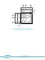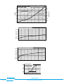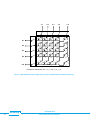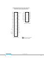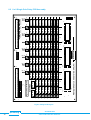
1
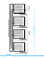
USER MANUAL
pickering
Model No. 20-520/20-525
R.F. Matrix Module with Self-Test
Designed & Manufactured by:Pickering Interfaces Limited.
Stephenson Road
Clacton-on-Sea
Essex
CO15 4NL
England
Tel:
Fax:
01255-428141
01255-475058
+44 1255-428141 (International)
+44 1255-475058 (International)
Internet: www.pickering.co.uk
E Mail: [email protected]
Issue 2.00 June. 1996
© Copyright (1996) Pickering Interfaces Ltd. All Rights Reserved
pickering
20-520/20-525
R.F. SWITCHING MATRIX MODULE
1
HELP!!!
If you need assistance with your Pickering Interfaces Switching
System: Switching problems, Programming or Integration within your Test
System. – Please ring Pickering Interfaces and ask for “Technical
Support”.
Alternatively you may fax, email or connect to our Internet Web Site.
A full set of operating manuals, application notes and software drivers is
available on CD ROM.
pickering
2
20-520/20-525
SWITCHING MATRIX MODULE
Contents
Section 1
High Density Matrix Modules ..................................................................................... 5
Section 2
Constructing Large Matrix Systems .......................................................................... 11
Section 3
Self Test ................................................................................................................... 15
Section 4
Programming ........................................................................................................... 17
Section 5
Connector Pin-Out Diagrams................................................................................... 19
Section 6
Front Panel Layout .................................................................................................. 21
Section 7
Reconfiguring Driver Card to Your Application ......................................................... 23
Section 8
Circuit Diagrams ...................................................................................................... 25
Section 9
Adapting Matrix for Analogue Bus Connection ........................................................ 41
Section 10
Electrical, Environmental, Mechanical & Firmware Specifications .......................... 43
pickering
20-520/20-525
R.F. SWITCHING MATRIX MODULE
3
pickering
4
20-520/20-525
SWITCHING MATRIX MODULE
Section 1
High Density Matrix Modules
1.1 Features
•
High Isolation RF Switching Matrix, Available in 16 x 4 and 8 x 8 Configurations.
•
•
Single Pole Version Available in 50Ω or 75Ω Version with 100MHz Bandwidth
Double Pole Version Available with 50Ω Triaxial Connectors.
•
•
•
Full Matrix Self-Test for Total Switch Contact Confidence.
On-Board Isolation Switches Remove Unused Crosspoint Rows/Columns.
Large Low Frequency Matrices Easily Built Up Using Internal 24 Pole Analogue Bus.
•
•
•
Up to 31 Matrix Modules May Be Cascaded to Form Matrices with Sizes to Over 2000 Crosspoints.
Very Large Partially Filled Matrices May Be Constructed When Used In Conjunction with 20-700 Series RF
Multiplexer Modules.
Front Panel Mounted BNC Co-Axial Connectors.
•
•
Two Reed Switch Types: Standard Dry or Ruthenium.
Switch up to 100Vd.c., 10W, 0.5A (1.2A carry).
1.1.1 Matrix Description
This manual covers all models in the 20-520 range of Very High Isolation Matrix Modules switching frequencies to beyond
100MHz, available in both 50Ω & 75Ω versions. Also suitable for high accuracy, low frequency instrumentation requiring
good isolation/noise performance. Built-In Self-Test gives complete switch confidence.
System 20 High Isolation RF Matrix Modules are intended for easy construction of high performance matrix switching
systems; modules may be simply cascaded to form matrices of almost any size.
Connections are made via industry standard BNC connectors. Larger low frequency matrices are easily constructed
using the internal 24 pole guarded analogue bus. Isolation Switches on each module remove all unselected columns
and rows from the system, maximising both isolation and RF performance.
Full Self-Test is performed both at power up and at any other time either manually or under program control. Self-Test
is of particular importance in large systems where relay contact integrity is a very major consideration. In the unlikely event
of relay failure (either high on-state or low off-state resistance) the front panel will indicate a fault. The diagnosis - including
the position of the suspect relay - will be indicated using the DIAGNOSTIC? command.
For a summary of switching capabilities please refer to tables 1.1 & 1.2.
This is a double height module and must be mounted into a double height (6U) case: Available case types: 10-934,
10-936 20-930 and 20-935.
1.1.2 Applications
Main applications will be for very high quality switching where standard matrix units have inadequate RF and isolation
performance, these include: high quality data acquisition (usually 2 pole with frequencies < 1MHz), RF matrices (1 pole
to beyond 100MHz), telecommunications and video applications (75Ω impedance) and high quality signal routing in
functional ATE systems.
1.1.3 Front Panel
The module front panels are illustrated in Section 6, they comprise of three elements:
Status Display, 4 LED Indicators:Power LED.
Active LED.
Connected to power system supply.
On whenever one or more matrix switches are closed. For a list of all active switches use the VIEW?
command.
Self-Test LED. Active when self-test in progress.
Error LED.
Indicates that error found during self-test.
Self-Test Button. Press to initiate a self-test, this will first disconnect the matrix, then perform a full functional self-test,
finally reconnecting the matrix when complete. While in progress the “Self-Test” LED will be on, if a failure is detected
then the “Error” LED will be set on permanently. Use the DIAGNOSTIC? command to find the exact cause of any failure,
refer to section 3 for further details. NB: Self-Test button will only respond when matrix is inactive (i.e. no crosspoints set).
Matrix Connectors. Provides connection to and from matrix, BNC Co-Axial and BNC Tri-Axial connectors, please refer
to Section 6.
pickering
20-520/20-525
R.F. SWITCHING MATRIX MODULE
5
Isolation
Switch
Y1 Y2 Y3 Y4 Y5 Y6 Y7 Y8
X1
X2
X3
X4
Matrix
Crosspoint
X5
X6
X7
X8
Fig 1.1 Matrix Schematic (8 x 8, 2 Pole)
Characteristic Impedance
50 or 75Ω
RF Specification For 1 Pole Version Only:
Maximum Frequency
200MHz
Rise Time
< 1nS †
Insertion Loss (< 100MHz)
< 3dB †
V.S.W.R. (< 70MHz)
< 1:1.8 †
Isolation (< 100MHz)
> 75dB
Crosstalk (< 100MHz)
> 60dB
Maximum Voltage
Maximum Power
Maximum Switch Current
Maximum Carry Current
100V d.c.
10W
0.5A
1.2A
On Path Resistance
< 500 mΩ
Off Path Resistance
> 109 Ω
Noise
< -75dBm
Differential Thermal Offset
< 20µV
Capacitance: Open Channel to Ground < 40pF
Capacitance: Selected Channel to Ground
< 70pF
Capacitance: Open Input to Output
< 4pF
Expected Life (Low Power)
Expected Life (Max Power)
> 1x10⁸ ops
> 5x10⁶ ops
Switching Time
< 10mS
Table 1.1 Switching Specification
† RF Performance is entirely dependant upon the combination of crosspoints currently selected, these figures are for one
selected crosspoint only, please refer to graphs in Sec 1.4.
pickering
6
20-520/20-525
SWITCHING MATRIX MODULE
1.2 Matrix Module Model Numbers
The following table lists the standard options available with the matrix module:Configuration
Connect
Type
Imdepance
No. of
Poles
Dry Reed
Switch
Low Level
Switch
16 x 4
BNC Coax
50Ω
1
20-520-501
20-520-521
16 x 4
BNC Triax
50Ω
2
20-520-502
20-520-522
16 x 4
BNC Coax
75Ω
1
20-520-701
20-520-721
8x4
BNC Coax
50Ω
1
20-522-501
20-522-521
8x4
BNC Triax
50Ω
2
20-522-502
20-522-522
8x4
BNC Coax
75Ω
1
20-522-701
20-522-721
8x8
BNC Coax
50Ω
1
20-525-501
20-525-521
8x8
BNC Triax
50Ω
2
20-525-502
20-525-522
8x8
BNC Coax
75Ω
1
20-525-701
20-525-721
Configuration Options † : –Y
Y Coordinates connected to analogue bus.
–X
X Coordinates connected to analogue bus
† Default configuration is no connections to internal analogue bus.
Further options (see notes below):
–R
Limiting Resistor (e.g. 20-525-701-R).
–L
Loop Through Option: All of the above modules are available
with a loop through option, see diagram, frequently used in the
construction of large self terminating RF matrices. Please order
option -L (e.g. 20-525-501-L)
Further options are available for interconnecting matrix modules to form very large
matrices, please contact factory to discuss your application in more detail.
All reed relay switching modules have the facility for a built in limiting resistor on each
switch. This can be very useful in preventing high current in-rushes which may result
in damage to the reed switch. These links are normally shorted, however when
ordering you may specify limiting resistors if you wish, option -R.
pickering
20-520/20-525
R.F. SWITCHING MATRIX MODULE
7
Y1
Y2
Y4
To Self Test
Circuit
X1
X2
X 16
To Self Test
Circuit
Fig 1.2 Full Schematic of 16 x 4 Single Pole Matrix Module
(104 Relays with 64 used in main Cross-Point Matrix)
pickering
8
20-520/20-525
SWITCHING MATRIX MODULE
1.3 Reed Switch & Connector Options
A summary of these modules capability is in tables 1.1 and 1.2.
Additional data is included below:1.3.1 Dry Reed Switch
Reed Relay Type
Expected Life
50Ω 1/2 Pole: 102M-1-A-12/1D
75Ω 1 Pole: 101-1-A-12/949D
> 108 operations at low current/voltage load.
> 5x10⁶ at 260mA, 28V.
1.3.2 Low Level Ruthenium Reed Switch - for low level signal use only
Reed Relay Type
50Ω 1/2 Pole: 102M-1-A-12/2D
75Ω 1 Pole: 101-1-A-12/949D SW 2
Expected Life >
108 operations at low current/voltage load.
NB This switch is not suitable for switching high current loads.
1.3.3 Front Panel and Connectors
Two connector types are currently available, both are front panel mounted:1 Pole Version
16 x 4 Matrix: 20 x BNC Coaxial Connector Sockets, see Fig 6.1.
8 x 8 Matrix: 16 x BNC Coaxial Connector Sockets, see Fig 6.2.
2 Pole Version
16 x 4 Matrix: 20 x BNC Triax Connector Sockets, see Fig 6.1.
8 x 8 Matrix: 16 x BNC Triax Connector Sockets, see Fig 6.2.
Module width is 12 HP (2.4 inches, 60.8mm).
Front Panel layouts are illustrated in Section 6.
1.4 Typical RF Performance Plots (Single Pole Versions)
Typical RF Performance Plots for 20-525-501 (8 x 8, Single Pole)
Curves are shown for matrix rows/columns with: 1 or 2 interconnected crosspoints set. For optimum insertion loss and
VSWR (reflection) performance ensure only one crosspoint is set in any one row/column.
Performance curves for all versions of the single pole matrix modules have similar characteristics, any differences are
shown. For further information please contact factory.
0 dB
20-525 MATRIX INSERTION LOSS
-0.4 dB
1 Crosspoint Set
-0.8 dB
-1.2 dB
-1.6 dB
-2.0 dB
-2.4 dB
-2.8 dB
2 Crosspoints Set
-3.2 dB
50MHz
pickering
100MHz
150MHz
200MHz
20-520/20-525
R.F. SWITCHING MATRIX MODULE
9
20-525 MATRIX VSWR
(RETURN LOSS)
VSWR
1.6
1 Crosspoint Set
(75Ohm Version)
13dB
1 Crosspoint Set
(50Ohm Version)
1.4
16dB
1.2
21dB
26dB
1.0
50MHz
100MHz
20-525 MATRIX ISOLATION
-50 dB
-60 dB
-70 dB
-80 dB
-90 dB
-100 dB
50MHz
100MHz
150MHz
200MHz
20-525 MATRIX CROSSTALK
-40 dB
-50 dB
-60 dB
-70 dB
-80 dB
-90 dB
-100 dB
50MHz
100MHz
150MHz
20-525 TYPICAL
90% STEP RESPONSE
(1 Crosspoint Set)
50%
0.7nS
10%
0.4nS
pickering
10
0.8nS
1.2nS
20-520/20-525
SWITCHING MATRIX MODULE
200MHz
Return Loss
11dB
1.8
Section 2
Constructing Large Matrix Systems
2.1 Creating Large Matrices
Each System 20 interface can directly support cascaded matrices up to 128x16 or 32x64 using 16x4 matrix modules or
up to 64x32 using 8x8 matrix modules, i.e. up to 31 modules per matrix, larger sizes can be supported using multiple
System 20 interface modules mounted in separate cases.
Forming larger matrices is usually only a question of plugging in additional matrix modules, a 24 pole guarded analogue
bus is provided on the System 20 Analogue Backplane. So constructing large matrices is very straight forward, no time
consuming daisy-chained wiring harnesses. Further expansion is simply a matter of adding additional matrix modules,
please refer to notes in Section 2.4.
All matrix modules in a cascaded matrix must have the same primary address, their position within the matrix is determined
by their bank address (see sec 4.2, figs 2.1 & 2.2), this is set on an additional 5 way dip switch. The cascaded matrix
is then programmed as a whole, the programmer does not need to address each matrix module individually, only a pair
of coordinates for the required crosspoint need be sent.
2.2 Isolation Switches
Both the X and Y axes have on-board automatic isolation switches. In large matrix systems the parasitic capacitance
associated with each cross-point switch can result in a large capacitance if several matrix modules are interconnected.
The isolation switches only switch in those columns and rows on a module that contain an active switch. Thereby keeping
matrix capacitance to a minimum., this may be important for applications requiring high isolation and crosstalk as well as
good insulation resistance.
NB. These isolation switches are also used to remove the matrix from the external circuit when performing self-test.
2.3 “Partially Filled” Matrices
For users requiring very large matrix systems the cost of a fully populated matrix may prove prohibitive, in many instances
a combination of multiplexer input/output and small “core” matrix may prove quite acceptable. This approach may prove
to be more effective in terms of both cost and performance, the main draw backs being additional programming complexity
and restricted matrix versatility (particularly for future unforeseen requirements). Please contact Pickering if you wish to
discuss your matrix application in greater detail.
Pickering can build large Matrix systems constructed and tested to your exact requirements, (especially if your application
involves switching RF or very high isolation signals), please contact sales office for further details.
2.4 Expanding an RF Matrix Using the Analogue Bus
If the signals being switches are not RF, typically < 1MHz bandwidth then using the analogue bus will be very
straightforward. However, if RF frequencies (>1MHz) are being switches then particular attention must be paid to matrix
interconnection.
If the analogue backplane bus is used to interconnect two or more matrices switching RF signals then return loss (VSWR)
will be very severely affected (e.g. around 10dB at around 10MHz), insertion loss will also be degraded This is due to the
effect of the long bus lines (typically 45cm in length). Performance can be maximised by interconnecting the matrix
modules using the front panel mounted Coaxial connectors or by ordering a system with a reduced length analogue
backplane bus (e.g. quarter length).
However if very low VSWR performance is required when switching RF signals, particularly in a large system, it may be
worth looking at the Pickering Interface’s range of RF multiplexers, these can be used to construct very high performance
matrix systems. Please contact factory for further information or advice.
pickering
20-520/20-525
R.F. SWITCHING MATRIX MODULE
11
Y1
Y2
Y3
Y4
Y8
X1
X2
X3
X4
X8
Crosspoints Closed are at x = 2, y = 2 & x = 2, y = 4.
Fig 2.1 Typical Matrix (8 x 8 Single Pole) in Use with Automatic Isolation Switching
pickering
12
20-520/20-525
SWITCHING MATRIX MODULE
8
6
3 4 5
1 2 3
1 2 3
4 5
4 5
8
8
4 5
4 5
8
8
8 x 8 Matrix
8 x 8 Matrix
R.F. SWITCHING MATRIX MODULE
Fig 2.2 32 x 8 Matrix Switch
32 Inputs
1 2 3
1 2 3
1 2
1 2
3 4 5
3 4 5
8
8
8 x 8 Matrix
1 2
1 2
8 Outputs
3 4 5
3 4 5
8 Poles of the internal guarded Analogue Bus are used to interconnect the 4 matrix modules. Additional matrix modules may be simply plugged
in to give further expansion.
1 2
8
6
3 4 5
1 2
8
6
3 4 5
1 2
8
6
3 4 5
pickering
1 2
INTERNAL 24 POLE ANALOGUE BUS
8
8
8 x 8 Matrix
20-520/20-525
13
pickering
14
20-520/20-525
SWITCHING MATRIX MODULE
Section 3
Self Test
3.1 Self-Test Function
Self-Test is invoked at power on (taking up to 60 seconds) and may also be operated under software (*TST?) or via a
recessed push button. Self-Test pass is indicated on a front panel LED with a full pass/fail description available using
the DIAGNOSTIC? command.
Self-Test comprises 3 levels, see Fig 3.1:1.
Logic Test: Checks all logic including on-board microprocessor, relay drivers etc.
2.
3.
(i)
Relay Coil Test: All reed relay coils are checked for continuity.
Full Contact Test: Tests all the relay contacts in the matrix block. Two test are undertaken:
On-state resistance failure test. Fails if switch has on-state > 2Ω.
(iii)
Off-state resistance test. A switch fails if it’s isolation resistance is < 106Ω.
The threshold for contact resistance is preset to approximately 2Ω at the factory. However this threshold may set to
customers precise requirements (from 200mΩ to 10Ω). If a very low threshold is selected, the self test could be used to
detect switches which are not failing to operate but which have reached an end of life condition, where the contact
resistance is starting to rise, indicating that the relay is due for replacement.
NB. The contact self test will only check the relay contacts in the core matrix block, isolation switches and self test switches
are not tested, please refer to section 3.4 for further details.
Note: Fault diagnosis on 2 pole matrix modules will identify down to a pair of relays. Both these relays must be replaced,
only the position of the first relay in the pair is given by the REPORT? command, please refer to Section 8.3.
3.2 Self-Test Operation
Self Test is always run at power on, taking approximately 60 seconds.
If self test is run under software control it will firstly clear the whole matrix (Manual Test will only function when the module
is in a clear state). So it is very important to prepare your external instruments and U.U.T. for this! During self-test all
isolation switches are opened so your external circuitry will see only very high resistance inputs.
When the self-test has finished the matrix will be returned to an all clear state (i.e. the previous state will not be
remembered!).
Please note that because of the long self-test time that your computer may time out waiting for the test result (many PC's
have default timeouts set to 10 seconds).
3.3 Detailed Self Test Reporting using DIAGNOSTIC? Query
The DIAGNOSTIC? query will give an ASCII string detailing any self test failures. These will include:Logic: µP, RAM, EPROM, Relay Drivers, Invalid Link Settings etc.
Relay Coils: Open Circuit Coil.
Switch Contacts:
High On Resistance, Low Off Resistance.
This string is not intended to be processed by the user’s software, it is suitable for copying directly onto the screen of your
control computer. This information will then indicate maintenance required (please contact Pickering for further help).
3.4 Self Test Limitations
Self Test covers all aspects of the Matrix Module which are liable to fail in normal use. The only exception to this are the
following:“Isolation Relays”: These switches are used to isolate the matrix from the users external circuitry, for this reason they
cannot be included in the contact self test routine, refer to fig 2.1. These relays always “cold switch” (i.e. they are always
operated without any load, as opposed to the matrix switches which always “hot switch”), therefore they should have an
expected life in excess of 108 operations. These switches will only fail if a very heavy current is passed through the contacts
(greater than around 3-4A for 10's of milliseconds, see section 5.1.1), this may result in switch weld to either an isolation
or matrix switch. Please note that all relays including isolation and self test relays are included in the coil test, so an open
circuit coil or faulty driver IC will be picked up and reported.
“Self Test Relays”: There are self test relays on every x and y axis on the matrix board, if one of these contacts welds
(very, unlikely) then all relays on that axis will appear to fail self test.
pickering
20-520/20-525
R.F. SWITCHING MATRIX MODULE
15
SELF TEST INITIATED BY:
• POWER ON
• *TST? QUERY
• MANUAL BUTTON
LOGIC TEST:
• µP BOARD
• RELAY BOARD
LOGIC
TEST FAIL
YES
NO
RELAY COIL TEST
COIL
TEST FAIL
YES
NO
CONTACT TEST:
• SWITCH ON STATE
RESISTANCE < 2Ω
• SWITCH OFF STATE
RESISTANCE > 1MΩ
CONTACT
TEST FAIL
YES
NO
SELF TEST PASS
SELF TEST FAIL:
• ERROR LED ON
• USE DIAGNOSTIC?
COMMAND TO GET
ERROR MESSAGE
Fig 3.1 Self-Test: Basic Flow Diagram
pickering
16
20-520/20-525
SWITCHING MATRIX MODULE
Section 4
Programming
4.1 Select Module Address
Choose module address (from 0 - 30) using the address select switch (SW1) on the top of the driver card (the top screen
of the module may need to be removed to reveal the address switch).
The module address selected in the illustration is 22 (i.e. 16 + 4 + 2 = 22).
4.2 Select Module Bank Address
When more than one module is used to make up a large matrix (see Fig 1.2), where four 20 x 12 modules are used to make
up a 40x24 matrix), then all matrix units must have the same module address, the location of each module within the matrix
is given by its bank address. The matrix bank address is composed of two x and y components, see Fig 1.3 , these
determine the individual matrix modules position within the larger matrix.
The bank address is constructed using 5 bits, see diagram, 3 bits for x and 2 bits for y. For example bit settings 0 0 1 0
0 represent bank address x = 1, y = 0.
16
bank address
8
4 2
SW1
module address
16 8
4 2 1
1
ON
1 2 3 4 5 6 7 8 9 10
1 2 3 4 5 6 7 8 9 10
PCB
Side View
Top View
There must always be a module present at the base address x = 0, y = 0, otherwise the matrix will not be recognised by
the intelligent interface.
If there is a problem with any of the modules used to make up a large matrix then an error will be detected (use the
DIAGNOSTIC? query to discover the cause).
4.3 Using the Intelligent GPIB Interface
X2 X1 X0 Y1 Y0
Switching matrices are controlled using the MCLOSE and MOPEN commands:To close switch at position X = 17, Y = 9 on matrix with address 11.
MCLOSE 11,17,9
Now to look at status of matrix 11.
VIEW? 11
will return “17,9”
To open last switch and close switches at positions X = 1, Y = 1 and X = 2, Y = 1 on matrix 11.
MOPEN 11,17,9;MCLOSE 11,1,1;MCLOSE 11,2,1
Now to look at status of matrix 11.
VIEW? 11
will return “1,1;2,1”
To reset all switches on matrix 11.
ARESET 11
Now to look at status of matrix 11.
VIEW? 11
will return “0,0" - 0,0 indicates no coordinates set.
Note: The 10-920 Interface imposes a maximum limit allowing up to 100 crosspoints to be on at any one time (this is to
prevent the power supply becoming overloaded).
pickering
20-520/20-525
R.F. SWITCHING MATRIX MODULE
17
4.4 Instruction Set
The Matrix module is very easy to program using the Model 10-920 IEEE-488.2 Interface:ARESET a Open all switches on device a
MCLOSE a,x,y
Close switch at coordinates x,y on matrix a
MOPEN a,x,y Open switch at coordinates x,y on matrix a
RESET
VIEW? a
Open all switches on all modules
View status of device a.
Self Test Functions:DIAGNOSTIC?
Return diagnostic string (self test fail details, if any). Refer to Sec 3.3 for further details
*TST? Execute Full Self Test (IEEE-488.2 query)
4.5 Operating Speed
Maximum switching frequency is approximately 25mS to open or close any one crosspoint when using the 10-920 IEEE488.2 Interface Module, the higher speed 10-921 interface reduces this time to 10mS.
pickering
18
20-520/20-525
SWITCHING MATRIX MODULE
Section 5
Connector Pin-Out Diagrams
ROW
A
C
1
2
3
4
5
6
7
8
9
10
11
12
13
14
15
16
17
18
19
20
21
22
23
24
25
26
27
28
29
30
31
32
Analogue 2.1
Analogue 2.2
Analogue 2.3
Ground
Analogue 2.4
Analogue 2.5
Analogue 2.6
Ground
Analogue 2.7
Analogue 2.8
Analogue 2.9
Ground
Analogue 2.10
Analogue 2.11
Analogue 2.12
Ground
Analogue 2.13
Analogue 2.14
Analogue 2.15
Ground
Analogue 2.16
Analogue 2.17
Analogue 2.18
Ground
Analogue 2.19
Analogue 2.20
Analogue 2.21
Ground
Analogue 2.22
Analogue 2.23
Analogue 2.24
Ground
A & C contacts are commoned. All
analogue bus lines are surrounded
by a grounded guard track to
minimise inter–channel crosstalk.
Analogue Bus Approximate RF
Characteristic Impedance = 65Ω.
Fig 5.1 24 Pole Internal Analogue Bus Connector
(Type: 64 Pin DIN 41612)
pickering
20-520/20-525
R.F. SWITCHING MATRIX MODULE
19
AAAAAAAA
AAAAAAAA
AAAAAAAA
AAAAAAAA
ROW
A
C
GND
5V(relay)
5V(logic)
DIO1
DIO3
EOI
NRFD
IFC
ATN
DIO5
DIO7
REN
Settled
Reserved (SCK)
Analogue 1.1
Analogue 1.2
Analogue 1.3
Analogue 1.4
Analogue 1.5
Analogue 1.6
Analogue 1.7
Analogue 1.8
Analogue 1.9
Analogue 1.10
Slot Address Bit 0
Slot Address Bit 2
Slot Address Bit 4
Backplane Address Bit 1
1
2
3
4
5
6
7
8
9
10
11
12
13
14
15
16
17
18
19
20
21
22
23
24
25
26
27
28
29
30
31
32
GND
12V(relay)
POWER SUPPLIES
5V(logic)
DIO2
DIO4
DAV
NDAC
SRQ
SYSTEM DIGITAL BUS
Reserved
(Parallel and Serial Bus)
DIO6
DIO8
Reserved (-SS)
Reserved (MOSI)
Reserved (MISO)
Analogue 1.1
Analogue 1.2
Analogue 1.3
Analogue 1.4
Analogue 1.5
ANALOGUE BUS
Analogue 1.6
Analogue 1.7
Analogue 1.8
Analogue 1.9
Analogue 1.10
Slot Address Bit 1
Slot Address Bit 3
POSITION
Backplane Address Bit 0
LOCATOR
Backplane Address Bit 2
AAAAAAAA
AAAAAAAA
AAAAAAAA
AAAAAAAA
AAAAAAAA
AAAAAAAA
AAAAAAAA
AAAAAAAA
AAAAAAAA
12V(relay)
5V(logic)
GND
12V(relay)
5V(logic)
GND
POWER SUPPLIES
10/92
Note: The Analogue bus on this connector is not used by any matrix module (only multiplexers).
All analogue bus lines are surrounded by a grounded guard track to minimise inter–channel crosstalk.
Analogue Bus Approximate RF Characteristic Impedance = 65Ω.
Fig 5.2 Power/Control/Analogue Bus Connector
(Type: 64 Pin DIN 41612)
pickering
20
20-520/20-525
SWITCHING MATRIX MODULE
Section 6
Front Panel Layout
LED (red) Module
powered on
X1
X2
POW
X3
X4
LED (green) Indicates
if any switch is
operated
ACT
TEST
X5
X6
X7
X 8 MAN
TEST
X9
X 10
X 11
X 12
X 13
X 14
X 15
X 16
Y1
Y2
Y3
Y4
LED (yellow) Self-Test
Currently Running
ERR
LED (red) error found
during self-test
Self-Test Switch
(recessed to prevent
accidental operation)
Fig 6.1 20-520 Front Panel, 16 x 4 Matrix
pickering
20-520/20-525
R.F. SWITCHING MATRIX MODULE
21
X1
X2
POW
X3
X4
ACT
TEST
ERR
X5
X6
MAN
TEST
X7
X8
Y1
Y2
Y3
Y4
Y5
Y6
Y7
Y8
Fig 6.2 20-525 Front Panel, 8 x 8 Matrix
pickering
22
20-520/20-525
SWITCHING MATRIX MODULE
Section 7
Reconfiguring Driver Card to Your Application
Your multiplexer driver card will leave the factory preconfigured, so take great care if you wish to change any of the
settings. If in doubt contact Pickering for further details.
7.1 Universal Driver Card: Configuration Links
Configuration switches are provided on the driver board at position SW2, on the top edge of the PCB, adjacent to the 10
way address selection lever switch. The five switches, see Fig 7.1, are used as follows:Relay Settling Time
There are four choices of relay settling time, this is to allow for different applications and relay types.
1
2
Relay Settling Time †
0
0
4.0ms
0
1
1
0
1.0ms - default setting
0.5ms
1
1
0.0ms
† The “Settled” line is triggered after this delay
Matrix Intelligent Isolation Switching
This will allow intelligent isolation switching, i.e. only those matrix rows and columns that have an active crosspoint switch
will be connected in circuit. Note intelligent isolation switching may operate a little slower (up to around 5ms per operation
because all isolation switches always cold switch).
3
0
4
–
5
–
Function
1 Pole Switching (used for self test only)
1
–
–
–
0
1
–
–
–
2 Pole Switching (used for self test only)
Enable Full Self Test (60 Seconds) - default setting
Enable Logic Only Self Test (5 Seconds)
–
–
–
–
0
1
Enable Automatic Isolation Switching - default setting
Disable Automatic Isolation Switching
7.2 Repeating Self Test with Burn In - Factory Use Only
A burn-in test facility is built into the module, this is initiated by pressing the selftest button until the Active LED goes on
(around 5 seconds). Here the module will run the usual full selftest together with some additional isolation tests followed
by 15 minutes of “switch rattling”, the test procedure will then be repeated. This process may only be stopped by powering
off or holding the manual test button in for several seconds.
This feature is for factory use where matrix modules are burned-in prior to undergoing final test.
5 4 3 2 1
O
N
SW2
Fig 7.1 Driver Card Configuration Links on SW2
pickering
20-520/20-525
R.F. SWITCHING MATRIX MODULE
23
pickering
24
20-520/20-525
SWITCHING MATRIX MODULE
Section 8
Circuit Diagrams
Two sets of circuit diagrams and documentation are contained:-
• 8.1 Driver PCB Assembly
PCB Layout
Circuit Diagram (6 pages)
Inter PCB Connectors
Parts List
• 8.2 8 x 8 Single Pole Relay PCB Assembly
PCB Layout
Inter PCB Connectors
Parts List
• 8.3 8 x 8 Double Pole Relay PCB Assembly
PCB Layout
Parts List
pickering
20-520/20-525
R.F. SWITCHING MATRIX MODULE
25
D.1 Driver PCB Assembly
C6
C8
C7
1 2 4 8 16 1 2 4 8 16
5 4 3 2 1
5 4 3 2 1
J1
BANK
SW1 ADDR
SW2
LD1
R4
R8
U8
k
LD2
U7
k
LD3
k
LD4
C9
Q3
U6
k
R9
C13
U9
Q4
X1
R23
R22
SW3
C2
J3
C1
+
J4
C3
U1
C4
Q1
U3
R7
R3
R2
R1
R5
U4
J2
C12
U5
R6
R16
R15
U2
R17
R11
C5
R18
U10
R21
Q2
R14
R10
R19
RL1 RL2 RL3 RL4
C10
R20
C11
pickering
Fig 8.1 Driver PCB Layout
pickering
26
20-520/20-525
SWITCHING MATRIX MODULE
pickering
20-520/20-525
R.F. SWITCHING MATRIX MODULE
27
C2
C1
GND
+5V
4
3
2
1
C6
GND
+5V
U1
GND
CT
C7
Vcc
-RESET
RESET
SENSE
7705
-RESIN
Vref
System 20 Driver Card - GPIB 80 Rev 0
C8
5
6
7
8
C9
R1
C10
C11
-RES
C12
C13
-LD4
-LD3
-LD2
14.11.90
Sheet 1 of 6
GND
R4
STAT
LD1
R2
LD2
Miscellaneous: Reset control, LEDs, Power Supply decoupling, 'Settled' line driver
LD3
R3
GND
+5V
Q1
LD4
+5V
STLD
pickering
28
20-520/20-525
SWITCHING MATRIX MODULE
-IRQ1
MODDATA
-LEAK1
-CTEST2
-DROP
-CTEST1
-LEAK2
Serial Debug
5
4
3
2
1
J3
SERCLK
IGIDATA
-LD4
-LD3
-LD2
GND
+5V
R23
+5V
Q4
GND
U5
R22
74HCT244
GND
2Y1
1A4
2Y2
1A3
2Y3
1A2
2Y4
1A1
-1G
GND
10
9
8
7
6
5
4
3
2
1
GND
2A1
1Y4
2A2
1Y3
2A3
1Y2
2A4
1Y1
-2G
Vcc
11
12
13
14
15
16
17
18
19
20
R5
+5V
+5V
+5V
SW3
INH
RDATA5
RDATA4
RDATA3
RDATA2
GND
R6
C3
-RES
GND
X1
STAT
C4
R7
+5V
STRB5
STRB4
STRB3
STRB2
STRB1
LDATA
LCLK
-STFAIL
14.11.90
Sheet 2 of 6
+5V
GND
+5V
CPU, address decoding, ROM and buffers
32
31
30
29
28
27
26
25
24
23
22
21
20
19
18
17
16
15
14
13
12
11
10
9
8
7
6
5
4
3
2
1
-WR
EXTAL
A15
Vcc
P67
A14
A13
A12
A11
A10
A9
A8
Vss
A7
A6
A5
A4
A3
A2
A1
A0
D7
D6
D5
D4
D3
P66
P65
P64
P63
P62
P61
P60
P57
P56
P55
P54
P53
P52
P51
P50
P27
P26
P25
P24
P23
P22
P21
D2
D1
P20
D0
BA
-NMI
-RES
-STBY
-LIR
MP1
R/-W
-RD
XTAL
MP0
E
6303X
U2
Vss
GND
System 20 Driver Card - GPIB 80 Rev 0
33
34
35
36
37
38
39
40
41
42
43
44
45
46
47
48
49
50
51
52
53
54
55
56
57
58
59
60
61
62
63
64
-GPIACS
-PIACS2
+5V
A15
A14
A13
A12
A11
A10
A9
A8
A7
A6
A5
A4
A3
A2
A1
A0
D7
D6
D5
D4
D3
D2
D1
D0
A14
A13
GND
D2
D1
D0
A0
A1
A2
A3
A4
A5
A6
A7
14
13
12
11
10
9
8
7
6
5
4
3
2
1
8
7
6
5
4
3
2
1
1Y1
1Y0
1B
1A
1G
Vss
D2
D1
D0
A0
A1
A2
A3
A4
A5
A6
A7
U3
2Y3
2Y2
74HCT139
Vss
1Y3
2Y1
2Y0
2B
2A
2G
Vcc
27256
16
9
10
11
12
13
14
15
D3
D4
D5
D6
D7
-CS
A10
-OE
A11
A9
A8
A13
Vcc
A14
U4
Vpp
A12
1Y2
GND
GND
A12
-WR
E
GND
+5V
15
16
17
18
19
20
21
22
23
24
25
26
27
28
+5V
A15
A10
A11
A9
A8
A13
A14
D3
D4
D5
D6
D7
pickering
20-520/20-525
R.F. SWITCHING MATRIX MODULE
29
-RES
E
-WR
-GPIACS
6
10
D3
13
14
D6
D7
20
19
18
17
16
15
12
D5
11
9
D4
8
D2
7
D1
D0
5
4
3
2
1
+5V
-IFC
RFD
Vcc
-SRQ
DAC
-REN
TRIG
-DAV
-RES
-EOI
DMA Req
T/-R2
-ATN
T/-R1
DB6
-IB7
-IB6
-IB5
-IB4
-IB3
-IB2
-IB1
DB7
DB5
DB4
DB3
DB2
DB1
DB0
E
-IB0
RS0
R/-W
RS1
-CS
-ASE
-IRQ
RS2
Vss
U6
DMA Gra
GND
21
22
23
24
25
26
27
28
29
30
31
32
33
34
35
36
37 A0
38 A1
39 A2
40
-IRQ1
GPIA, bus transceivers
14.11.90
Sheet 3 of 6
System 20 Driver Card - GPIB 80 Rev 0
12
11
10
9
8
7
6
5
4
3
2
1
12
11
10
9
8
7
6
5
4
3
2
1
Bus 0
Bus 5
Data 5
GND
Bus GND
Logic GND
3447
S/-R (7)
Bus 7
Data 7
S/-R (6)
Bus 6
Data 6
S/-R (1-4)
Bus 4
Data 4
S/-R (5)
Bus 3
Bus 2
Bus 1
Bus 0
Vcc
Data 3
Data 2
Data 1
Data 0
S/-R (0)
S/-R (7)
Bus 7
Bus 6
Bus GND
GND
U8
Bus 5
Bus 4
Bus 3
Bus 2
S/-R (1-4)
3447
Logic GND
S/-R (6)
Data 7
Data 6
S/-R (5)
Data 5
Data 4
Data 3
Data 2
Bus 1
Data 0
Data 1
Vcc
U7
S/-R (0)
24
13
14
15
16
17
18
19
20
21
22
23
24
13
14
15
16
17
18
19
20
21
22
23
+5V
+5V
REN
ATN
NRFD
DIO8
DIO6
DIO4
DIO2
SRQ
IFC
EOI
NDAC
DIO7
DIO5
DIO3
DIO1
DAV
pickering
30
20-520/20-525
SWITCHING MATRIX MODULE
Secondary Address
Primary Address
LSB
MSB
LSB
MSB
GND
5
4
3
2
1
10
9
8
7
6
5
4
3
2
1
SW2
SW1
RDATA1
+5V
R8
-CTEST1
R9
PIA, selector switches
14.11.90
Sheet 4 of 6
GND
+5V
20
19
18
17
16
15
14
13
12
11
10
9
8
7
6
5
4
3
2
1
-CS2
CS0
R/-W
CB2
Vcc
CS1
EN
D7
CB1
PB7
PB6
PB5
D6
D5
PB3
PB4
D4
PB2
D2
D1
D0
-RES
RS1
RS0
-IRQB
-IRQA
CA2
CA1
D3
6321
U9
PB1
PB0
PA7
PA6
PA5
PA4
PA3
PA2
PA1
PA0
Vss
GND
-LEAK1
System 20 Driver Card - GPIB 80 Rev 0
21
22
23
24
25
26
27
28
29
30
31
32
33
34
35
36
37
38
39
40
D7
D6
D5
D4
D3
D2
D1
D0
A12
A1
A0
GND
-WR
-PIACS2
E
-RES
pickering
20-520/20-525
R.F. SWITCHING MATRIX MODULE
31
-CTEST1
R10
VSEL
R11
R12
GND
Q2
Q3
TSTGND
TST2
TST1
R13
-LEAK2
-DROP
-CTEST2
R14
R15
VREL
RL4
RL3
RL2
RL1
Self-test analog circuits
14.11.90
Sheet 5 of 6
R16
R17
System 20 Driver Card - GPIB 80 Rev 0
C5
R19
R18
4
3
2
1
V-
IN+
IN-
OUT
NULL
V+
NULL STRB
U10
R20
5
6
7
8
GND
-STFAIL
R21
+5V
pickering
32
20-520/20-525
SWITCHING MATRIX MODULE
21
16
33
STRB2
15
32
SERCLK
LCLK
RDATA1
STRB1
LDATA
INH
MODDATA
17
Primary Serial Loop
Internal Bus and
RDATA2
RDATA3
RDATA4
RDATA5
TST2
STRB5
TSTGND
TST1
STRB4
STRB3
7
14
14
31
34
5
6
13
13
30
IGIDATA
4
11
12
12
29
3
and Self-Test
Secondary Serial Loops
10
2
11
1
28
9
STLD
10
27
J2
DIO8
8
8
26
DIO6
9
7
25
(for display)
24
6
5
4
GND
Serial Loop No 5
6
5
4
3
2
1
ATN
22
3
2
19
20
1
18
J4
IFC
VSEL
J1
+5V
23
GND
+5V
VREL
Sheet 6 of 6
14.11.90
Inter-PCB Connectors
System 20 Driver Card - GPIB 80 Rev 0
NRFD
EOI
DIO3
DIO1
DIO2
DIO4
DAV
NDAC
SRQ
DIO5
DIO7
REN
The pin rows of connectors J1, J2 are interchanged
relative to their physical positions.
Note :-
GPIB80 System 20 Driver Card inter-PCB
connectors (from component side)
LCLK
1
8
LDATA
+5v
RDATA2
2
9
STRB2
3 20
DIO1
RDATA3
3
10
STRB3
DIO4
4 21
DIO3
RDATA4
4
11
STRB4
DAV
5 22
EOI
RDATA5
5
12
STRB5
NDAC
6 23
NRFD
TSTGND
6
13
INH
SRQ
7 24
IFC
7
14
TST1
DIO5
8 25
ATN
DIO7
9 26
DIO6
REN
10 27
DIO8
GND
11 28
STLD
LCLK
12 29
LDATA
RDATA1
13 30
STRB1
INH
14 31
GND
MODDATA
15 32
IGIDATA
SERCLK
16 33
NC
NC
17 34
NC
VREL
1 18
VSEL (+12v)
GND
2 19
DIO2
TST2
Primary connector
pickering
Secondary connector
Note :
Pin numbering is PIL convention
only (not industry standard)
20-520/20-525
R.F. SWITCHING MATRIX MODULE
33
Parts List for GPIB80 Rev0 PCB Assembly
PCB
Location
PIL Part
Number
Part
Description
R1
R2
R3
R4
R5
R6
R7
R8
R9
R10
R11
R12
R13
R14
R15
R16
R17
R18
R19
R20
R21
R22
R23
C/RS/012
C/RS/012
C/RS/012
C/RS/016
C/RS/012
C/RS/013
C/RS/012
C/RS/013
C/RS/013
C/RS/025
C/RS/012
C/RS/024
C/RS/025
C/RS/026
C/RS/027
C/RS/025
C/RS/024
C/RS/012
C/RS/005
C/RS/024
————
C/RS/012
C/RS/012
Res
Res
Res
Res
Res
Res
Res
Res
Res
Res
Res
Res
Res
Res
Res
Res
Res
Res
Res
Res
Omit
Res
Res
Q1
Q2
Q3
Q4
C/SC/001
C/SC/001
C/SC/018
C/SC/001
Transistor
Transistor
Transistor
Transistor
BC182L
BC182L
RFP 12P08
BC182L
RL1
RL2
RL3
RL4
C/RL/000
C/RL/000
C/RL/000
C/RL/000
Reed
Reed
Reed
Reed
109-1-A-5/2D
109-1-A-5/2D
109-1-A-5/2D
109-1-A-5/2D
U1
U2
U3
U4
U5
U6
U7
U8
U9
U10
C/IC/019
C/IC/018
C/IC/028
C/IC/024
C/IC/033
C/IC/020
C/IC/021
C/IC/021
C/IC/016
C/IC/037
IC
IC
IC
IC
IC
IC
IC
IC
IC
IC
C1
C2
C3
C4
C5
C6
C7
C8
C9
C10
C11
C12
C13
C/CP/009
C/CP/005
C/CP/010
C/CP/010
C/CP/005
C/CP/003
C/CP/001
C/CP/001
C/CP/001
C/CP/001
C/CP/001
C/CP/001
C/CP/001
Cap
Cap
Cap
Cap
Cap
Cap
Cap
Cap
Cap
Cap
Cap
Cap
Cap
SW1
C/SW/005
DIP Switch
pickering
34
6k8Ω
6k8Ω
6k8Ω
8-pin
6k8Ω
9-pin
6k8Ω
9-pin
9-pin
22kΩ
6k8Ω
180kΩ
22kΩ
470kΩ
470RΩ
22kΩ
180kΩ
6k8Ω
180RΩ
180kΩ
5% 1/4W
5% 1/4W
5% 1/4W
SIP, 4 x 330R separate
5% 1/4W
SIP, 8 x 10k commoned
5% 1/4W
SIP, 8 x 10k commoned
SIP, 8 x 10k commoned
5% 1/4W
5% 1/4W
5% 1/4W
5% 1/4W
5% 1/4W
5% 1/4W
5% 1/4W
5% 1/4W
5% 1/4W
5% 1/4W
5% 1/4W
6k8Ω
6k8Ω
5%
5%
Relay
Relay
Relay
Relay
1/4W
1/4W
DIG 7705
DIG 63B03X
DIG 74HCT139
DIG 27256 EPROM
DIG 74HCT244
DIG 68488P
DIG 3447
DIG 3447
DIG 63B21
LIN CA3140E
10uF elect
100nF
22pF
22pF
100nF
22uF tant
10nF
10nF
10nF
10nF
10nF
10nF
10nF
10-pole dip piano key
20-520/20-525
SWITCHING MATRIX MODULE
SW2
C/SW/001
DIP Switch
SW3
C/SW/004
Switch
LD1
LD2
LD3
LD4
C/SC/004
C/SC/007
C/SC/004
C/SC/008
LED
LED
LED
LED
X1
C/MS/000
Xtal 4.00 MHz
J1
J2
J3
J4
C/CN/097
C/CN/077
————
C/CN/110
34-way pin header (2 row, gold pl.)
14-way pin header (2 row, gold pl.)
C/PC/086
PCB
pickering
5-pole dip slide
1pst p/button
(red)
(green)
(red)
(yellow)
6-way pin header (1 row)
6U
PTH
20-520/20-525
R.F. SWITCHING MATRIX MODULE
35
8.2 8 x 8 Single Pole Relay PCB Assembly
B
J
4
BB8 B8 8
BB2
4
BB2
3
BB2
2
BB2
1
BB2
0
BB1
9
BB7 B7
BB1
8
BB1
7
BB1
6
BB1
5
BB1
4
BB1
3
BB6 B6
BB1
2
BB1
1
BB1
0
BB
9
1
2
3
4
5
6
7
8
9
1
0
U
3
K
B
7
J
B
6
H
S Out
B
BB5 B5 5
C
5
G
U
2
B
BB4 B4 4
J
3
C
6
F
B
BB3 B3 3
E
B
BB2 B2 2
J
1
D
C
3
B
C
4
U
1
BB1 B1 1
C
J
2
RL
97
B
S In
RL
98
A
F
1
F
2
F
3
F
4
F
5
F
6
F
7
F
8
Fig 8.8 Relay PCB Layout
pickering
36
20-520/20-525
SWITCHING MATRIX MODULE
5
V
C
1
12
V
C
2
System 20 Relay Card inter-PCB
connectors (from component side)
NC
NC
34 17
33
16
NC
SERCLK (14a)
TST1
14
7
TST2
INH
13
6
TSTGND
STRB5
12
5
RDATA5
IGIDATA (13c)
32 15
MODDATA (14c)
GND (1a, c)
31 14
INH
STRB4
11
4
RDATA4
STRB1
30 13
RDATA1
STRB3
10
3
RDATA3
LDATA
29
12
LCLK
STRB2
9
2
RDATA2
STLD (13a)
28
11
GND (1a, c)
LDATA
8
1
LCLK
DIO8 (11c)
27
10
REN (12a)
DIO6 (10c)
26
9
DIO7 (11a)
ATN (9a)
25
8
DIO5 (10a)
IFC (8a)
24
7
SRQ (8c)
NRFD (7a)
23
6
NDAC (7c)
EOI (6a)
22
5
DAV (6c)
DIO3 (5a)
21
4
DIO4 (5c)
DIO1 (4a)
20
3
DIO2 (4c)
19
2
GND (1a, c)
18
1
VREL
+5v (3a, c)
VSEL (+12v) (4c)
Primary connector
backplane bus pin connects in
brackets
Secondary connector
Note :
Pin numbering is PIL convention
only (not industry standard)
Parts List for GPIB86 Rev0 Relay (1 Pole) PCB Assembly
PCB
Location
PIL Part
Number
Part
Description
J1, J4
J3
J2
B1..B8
F1..F8
C/CN/001
C/CN/077
C/CN/000
C/CN/118
C/CN/118
Connector DIN 41612 64 Way A/C
Header 14 pin 2 row
Header 34 pin 2 row
PC Mount Dielectric FeedThru 2, 6/50
PC Mount Dielectric FeedThru 2, 6/50
C1..C6
C/CP/001
Cap
RL1..RL98
U1..U3
C/IC/026
C/PC/086
pickering
10nF
RF Reed Relay See Sec 1.3 for type
IC DIG UCN 5818A
PCB 6U 4 Layer
20-520/20-525
R.F. SWITCHING MATRIX MODULE
37
8.3 8 x 8 Double Pole Relay PCB Assembly
24 B8.2
23
B8.1
K
d
c
22
L-T
21
20
1A
19
18 B7.2
17
16
B7.1
1C
J
d
c
1
L-T
15
14
13
12
11
10
1A
C9 C10
B6.2
B6.1
H
d
c
U4
L-T
9
8
7
C7 C8
B5.2
B5.1
G
d
c
6
5
4
L-T
1
3
2
1
J4
B4.2
B4.1
F
d
c
U3
L-T
B3.2
J3
B3.1
E
d
c
L-T
B2.2
1
B2.1
D
d
c
L-T
B1.2
C5 C6
U2
B1.1
C
d
c
C3 C4
L-T
19
20
1
B
C1
C2
1
U1
2
RL193
RL194
b
b
b
b
b
b
b
b
b
b
b
b
b
b
b
b
a
a
a
a
a
a
a
a
a
a
a
a
a
a
a
a
A
L-T
L-T
3
4
5
6
7
8
9
10
11
12
13
14
15
16
17
18
L-T
L-T
F1.
1
F2.
1
F3.
1
F4.
1
F5.
1
F6.
1
F7.
1
F8.
1
L-T
L-T
J2
J1
L-T
F1.
2
F2.
2
F3.
2
F4.
2
F5.
2
F6.
2
F7.
2
F8.
2
L-T
Note: Self Test Fails are diagnosed down to a pair of reed relays (so both relays must be removed), the pairs are shown
above.
pickering
38
20-520/20-525
SWITCHING MATRIX MODULE
Parts List for GPIB110 Rev0 Relay (2 Pole) PCB Assembly
PCB
Location
PIL Part
Number
Part
Description
J1, J4
J2
J3
C/CN/001
C/CN/124
C/CN/128
Connector DIN 41612 64 Way A/C
34 Way Mini-DIP Transition Connector
14 Way Mini-DIP Transition Connector
B1..B8
F1..F8
C/CN/118
C/CN/118
PC Mount Dielectric FeedThru 2, 6/50
PC Mount Dielectric FeedThru 2, 6/50
C1, C2
C3..C10
C/CP/003
C/CP/001
Cap Tant 22uF 16V
Cap Cer 10nF 50V
RL(A3-K20),195,196
RL193,194,197 C/RL/057
RF Reed Relay, See Sec 1.3 for type
107-1-C-12/3D
U1..U4
C/IC/035
IC
DIG
C/PC/110
PCB
6U
pickering
UCN 5818EPF
4 Layer
20-520/20-525
R.F. SWITCHING MATRIX MODULE
39
pickering
40
20-520/20-525
SWITCHING MATRIX MODULE
Section 9
Adapting Matrix for Analogue Bus Connection
9.1 Configuring Matrix for Analogue Bus Connection
All RF matrix modules are shipped from the factory configured for front panel interconnection (please refer to Sec 2.5),
therefore if the analogue bus is to be used then the module should be ordered in that configuration or the module must
be modified by the user.
To reconfigure the matrix module for analogue bus connection for a single pole 8 x 8 matrix:• Remove all Coaxial Launchers, locations B1, B2,...... B8 on relay PCB.
• Connect links BB8 to B8, BB7 to B7 .........BB1 to B1.
The operation is similar for 16 x 4 and all double pole versions. Please contact factory if you require further information
or assistance, module can also be returned to Pickering for modification.
pickering
20-520/20-525
R.F. SWITCHING MATRIX MODULE
41
pickering
42
20-520/20-525
SWITCHING MATRIX MODULE
Section 10
Electrical, Environmental, Mechanical & Firmware Specifications
Environmental
Operating Temperature 0°C to 50°C.
Storage Temperature -20°C to 75°C.
Humidity 95% non condensing.
Weight Dimensions and Power Requirements
Approx. Weight/g
1000
Dimensions/mm †
Front Panel Width
60.5
Height
268
Overall Length
189
Power /Current
Consumption
Maximum 5V
/mA
12V
250
1000
Minimum
150
0
5V
12V
† Approx. dimensions. Standard 160mm, 6U, Eurocard, as specified in DIN 41494.
Voltage Supplies
Logic Supply 5Vdc ±5%.
Relay Supply 12Vdc ±10%
Current Firmware Revision: 2.00
pickering
20-520/20-525
R.F. SWITCHING MATRIX MODULE
43
pickering
44
20-520/20-525
SWITCHING MATRIX MODULE