1
US007689815B2
(12) Umted States Patent
(10) Patent N0.:
Moyer et al.
(54)
(45) Date of Patent:
DEBUG INSTRUCTION FOR USE IN A DATA
2001/0032305 A1
PROCESSING SYSTEM
2003/0074650 A1*
2005/0240820 A1
(75)
Inventors: William C. Moyer, Dripping Springs,
TX (US); Michael D- Snyder, Cedar
Mar. 30, 2010
10/2001 Barry
4/2003
Akgul et al. .............. .. 717/129
10/2005 Vannerson et al.
2007/0050682 A1
3/2007 Takuma et al'
OTHER PUBLICATIONS
Park, TX (U S); Gary L. Whisenhunt,
Leander TX (Us)
PCT/US2008/075581 International Search Report andWritten Opin
’
~
US 7,689,815 B2
ion, Mar. 13, 2009.
_
-
-
EJTAG Speci?caton Revision 3.10; Jul. 5, 2005; 153 pages; MIPS
(73) Ass1gnee. 521E351? Semiconductor, Inc, Aust1n,
Technologies; Mountain View, CA‘
User’s Manual Version 1.1; “Microcontrollers on Chip-Debug-Sup
.
_
.
(*) Nonce'
.
.
.
“e2006Z6 PoWerPC Core Reference Manual”; Jun. 2004; Cover
Patent 15 extended or adlusted under 35
Page, Information Page, Table of Contents, and pp. 10-10thru10-25;
U~S~C- 15403) by 340 days-
Freescale Semiconductor, Inc.
(21) Appl. N0.: 11/871,847
.
* Cited by examiner
_
Primary ExamineriWilliam M Treat
(22) Flled'
Oct‘ 12’ 2007
(65)
(74)Allorney, Agent, orFirmiloanna G. Chiu; Susan C. Hill
Prior Publication Data
US 2009/0100254 A1
(51) Int CL
G06F 11/36
(52)
(58)
port”; Aug. 2001; 64 pp; In?neon Technologies.
SubJeCt_tO any dlsclalmerithe term Ofthls
(57)
Apr. 16, 2009
ABSTRACT
_
_
_
_
_
_
A method 1ncludes prov1d1ng a debug 1nstruct10n and prov1d
(200601)
ing a debug control register ?eld, Where if the debug control
register ?eld has a ?rst value, the debug instruction executes
us. Cl. .......................... .. 712/227- 714/35- 714/38
Field of Classi?cation Search
’
7,1202?
a debug Operation and Where ifthe debug Control register ?eld
has a second value, the debug instruction is to be executed as
"""""""" "714/35 38’
See a
lication ?le for Com lete Search histo
pp
p
References Cited
(56)
’
ry'
a no-operation (NOP) instruction. A data processing system
includes instruction fetch circuitry for receiving a debug
instruction, a debug control register ?eld, and debug execu
tion control circuitry for controlling execution of the debug
U'S' PATENT DOCUMENTS
5,491,793 A
2/1996 Somasundamm et a1‘
6,289,300 B1
9/2001 Brannick et a1‘
instruction in a ?rst manner if the debug control register ?eld
has a ?rst value and in a second manner if the debug control
register ?eld has a second value, Where in the ?rst manner a
debug operation is performed and in the second manner no
6,587,967 B1 *
7/2003 Bates et a1. ................. .. 714/35
debug Operation is Performed
7,240,185 B2 *
7/2007
7,444,547 B2 *
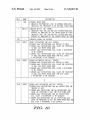
dnh
dui, duis
0
5 5
010011
Cofler et al. .............. .. 712/227
10/2008 Abou-Emara et a1. ....... .. 714/38
10 ll
dui
20 21
duis
30 31
0011000110E?
14 Claims, 6 Drawing Sheets
dnh2
dui, duis, group
0
5 6
|010011
10 11
du1
1718
duis
20 21
30 31
|group|0011000110€1?
US. Patent
Mar. 30, 2010
Sheet 1 of6
US 7,689,815 B2
10 x
14
a
EXTERNAL
PROCESSOR
<
~
DEBUG
CIRCUITRY
E
M
A
20
<
/
T
:
V
MEMORY
1/0
E
40
K
DEBUG
PORT
‘
E
22
INTERNAL
L INSTRUCTION =
DEBUG
PIPE
CIRCUITRY
I
DEBUG
‘ 421 "
T
T
{44
§
26
CONTROL
GENERAL
Z
CIRCUITRY
PURPOSE
INSTRUCTION
3
DEBUG
‘k
~
CONTROL
30
REGISTERS
FETCH UNIT
§ 32
<
CIRCUITRY
:
LL: LOAD/STORE <_
:
UNIT
8 ~
P RESET
I
‘k
24
I
“
UNITS
j
<
REGISTERS
‘4
EXECUTION
<
~
35
BIU
g
“
PROCESSOR
K
64L?
F]G. 2
20
12
US. Patent
Mar. 30, 2010
Sheet 2 of6
US 7,689,815 B2
42 \
INSTRUCTION ADDRESS
COMPARE
DEBUC CONTROL
50“
45
DBCRO
DBCR1
IAC1
IAC2
45
DDCR2
DBCR3
DBCR4
DEBUC STATUS
DBSR
x49
DATA ADDRESS COMPARE
47
DAC1
DACZ
51
DEBUC COUNTER
DBCNT1
DBCNT2
DATA VALUE COMPARE
53
DVC1
W02
EXTERNAL DEBUG
CONTROL
EDBCRO
EDBCR1
FIG. 4
50
US. Patent
Mar. 30, 2010
dnh
dui, duis
0
5 6
Sheet 3 of6
1011
010011
US 7,689,815 B2
2021
dui
duis
30 31
00110001100
FIG. 5
dnh2
dui, duis, group
0
5 6
1011
010011
1718
dui
duis
20 21
30 31
gr0up00110001101
DBCRAFN
0
15 16
—
17 18
GRP7C
19 20
GRP6C
2122
GRPSC
23 24
GRP4C
FIG. 7
25 26
GRPBC
27 28
GRPZC
29 30
GRP1C
51
GRPOC
US. Patent
Mar. 30, 2010
Sheet 4 of6
US 7,689,815 B2
BITS
NAME
0:15
—
16:17
GRP7C
CROUPT CONTROL
GRP6C
00 OROUPT dnhZ INSTRUCTIONS CENERATE A DEBUC
INSTRUCTION EXCEPTION
O1 GROUP7 dnhZ INSTRUCTIONS ARE TREATED AS NOPS
1X RESERVED
GROUP6 CONTROL
18:19
DESCRIPTION
RESERVED
OO CROUPO dnh2 INSTRUCTIONS CENERATE A DEBUC
INSTRUCTION EXCEPTION
O1 OROUPO dnh2 INSTRUCTIONS ARE TREATED AS NOPS
1X RESERVED
50:51
GRPOC
CROUPO dnhZ CONTROL
OO GROUPO dnh2 INSTRUCTIONS AND ALL dnh INSTRUCTIONS
CENERATE A DEBUC INSTRUCTION EXCEPTION
O1 OROUPO dnh2 INSTRUCTIONS AND ALL dnh
INSTRUCTIONS ARE TREATED AS NOPS
1x RESERVED
O
1
EDM DNH_EN
2
15 16
-
17 18
19 20
21 22
23 24
25 26
2728
29 3O
31
GRP7C GRP6C CRP5C GRP4C GRPSC CRP2C ORP1C GRPOC
FIG. .9
US. Patent
Mar. 30, 2010
Sheet 5 of6
US 7,689,815 B2
BITS
NAME
DESCRIPTION
0
EDM
EXTERNAL DEBUG MODE
O INDICATES THE PROCESSOR IS NOT IN EXTERNAL DEBUG MODE
1 INDICATES THE PROCESSOR IS IN EXTERNAL DEBUG MODE
1
DNH_EN
DEBUGGER NOTIFY HALT ENABLE
O INDICATES THAT THE dnh AND dnhZ INSTRUCTIONS WILL
OPERATE AS INDICATED BY THE DBCR4 GROUP SETTINGS
1 INDICATES THAT THE dnh AND dnhZ INSTRUCTIONS WILL
OPERATE AS INDICATED BY THE EDBCRO GROUP SETTINGS
2:15
—
16:17
GRP7C
GROUP7 WATCHPOINT AND HALT CONTROL
OO GROUP7 dnhZ INSTRUCTIONS ARE TREATED AS NOPS
O 1 GROUP7 dnh2 INSTRUCTIONS WILL CAUSE THE PROCESSOR
TO HALT AND ENTER DEBUG MODE
1O GROUP7 dnhZ INSTRUCTIONS WILL CAUSE A WATCHPOINT
TO BE SIGNALED
1 1 GROUP7 dnh2 INSTRUCTIONS WILL CAUSE THE PROCESSOR
TO HALT AND ENTER DEBUG MODE AND WILL CAUSE
A WATCHPOINT TO BE SIGNALED
18:19
GRP6C
GROUP6 WATCHPOINT AND HALT CONTROL
OO GROUP6 dnh2 INSTRUCTIONS ARE TREATED AS NOPS
O 1 GROUP6 dnh2 INSTRUCTIONS WILL CAUSE THE PROCESSOR
TO HALT AND ENTER DEBUG MODE
1O GROUP6 dnh2 INSTRUCTIONS WILL CAUSE A WATCHPOINT
TO BE SIGNALED
1 1 GROUP6 dnh2 INSTRUCTIONS WILL CAUSE THE PROCESSOR
TO HALT AND ENTER DEBUG MODE AND WILL CAUSE
A WATCHPOINT TO BE SIGNALED
30:31
GRPOC
GROUPO dnhZ WATCHPOINT AND HALT CONTROL
OO GROUPO dnh2 INSTRUCTIONS AND dnh INSTRUCTIONS ARE
TREATED AS NOPS
O 1 GROUPO dnhZ INSTRUCTIONS AND dnh INSTRUCTIONS WILL
CAUSE THE PROCESSOR TO HALT AND ENTER DEBUG MODE
1O GROUPO dnh2 INSTRUCTIONS AND dnh INSTRUCTIONS
WILL CAUSE A WATCHPOINT TO BE SIGNALED
1 1 GROUPO dnh2 INSTRUCTIONS AND dnh INSTRUCTIONS WILL
CAUSE THE PROCESSOR TO HALT AND ENTER DEBUG MODE AND
WILL CAUSE A WATCHPOINT TO BE SIGNALED
RESERVED, SHOULD BE CLEARED
FIG. 10
US. Patent
Mar. 30, 2010
Sheet 6 of6
US 7,689,815 B2
FROM
INSTRUCTION
FETCH UNIT
PORTION OF
CONTROL CIRCUITRY
26
J8
DECODE
CIRCUITRY
62
’
z
60
‘
DEBUG
EXECUTION
CONTROL
CIRCUITRY
FROM
42
4w; DEBUG REGISTERS
CONTROL SIGNALS
TO PORTIONS OF
PROCESSOR 12
dnhZ (group=0)
dnh2 (qroup=2)
dnh
_
—
YTRATl?-l —
—
_
_
—
—
—
—
—
—_ —
dnhz (gmup=0)
dnh2 (group-1)
TAR'GET
dnhZ (qroup=2)
_
US 7,689,8l5 B2
1
2
DEBUG INSTRUCTION FOR USE IN A DATA
PROCESSING SYSTEM
changes the execution characteristics of the system. That is,
the code image itself changes since branch targets, page
boundaries, and other instruction relationships may change
BACKGROUND
upon removal of the debug instructions. In order to allow the
code image itself to remain unchanged and thus possibly
1. Field
tems, and more speci?cally, to a debug instruction for use in
provide for more predictable execution, one embodiment dis
cussed herein provides additional control to allow debug
instructions to operate as “no-op” instructions (also referred
a data processing system.
to as no-operation instructions or NOPs) or to be suppressed
This disclosure relates generally to data processing sys
from execution. This allows for the debug instructions to
remain in place during application execution in which no
debugging is to be performed, where any debug instruction
2. Related Art
Debug instructions are commonly used during software
development to allow debug operations to take place. Once
the software has been developed and checked with debug
can be treated as a NOP, where NOPs may operate as known
instructions, these debug instructions are removed so as not to
in the art, or where the execution of the debug instruction may
cause undesired exceptions in the software application. How
ever, removal of these debug instructions can change the
execution characteristics of the system which may result in
be suppressed, such that no debug operation is performed,
even though the instruction has debug-related execution
semantics.
Also, in one embodiment, a class of debug instructions
less predictable execution. This may be especially problem
atic in real-time applications.
allow for grouping of debug instructions into independent
20
BRIEF DESCRIPTION OF THE DRAWINGS
The present invention is illustrated by way of example and
is not limited by the accompanying ?gures, in which like
references indicate similar elements. Elements in the ?gures
ing additional debug ?exibility. These groups may be inde
pendently controlled, and the resulting actions may be
dynamically modi?ed by either the hardware or software
25
are illustrated for simplicity and clarity and have not neces
of signals or conductors which may be used to transfer one or
more various types of information, such as data, addresses,
30
data processing system of FIG. 1, in accordance with one
embodiment of the present invention.
35
separate unidirectional conductors may be used rather than
bidirectional conductors and vice versa. Also, plurality of
conductors may be replaced with a single conductor that
transfers multiple signals serially or in a time multiplexed
manner. Likewise, single conductors carrying multiple sig
nals may be separated out into various different conductors
40
carrying subsets of these signals. Therefore, many options
exist for transferring signals.
The terms “assert” or “set” and “negate” (or “deassert” or
“clear”) are used herein when referring to the rendering of a
signal, status bit, or similar apparatus into its logically true or
45
logically false state, respectively. If the logically true state is
a logic level one, the logically false state is a logic level Zero.
And if the logically true state is a logic level Zero, the logically
false state is a logic level one.
accordance with one embodiment of the present invention.
FIG. 10 shows, in a tabular form, functionality of a portion
of the external debug control register of FIG. 9, in accordance
with one embodiment of the present invention.
FIG. 11 illustrates a block diagram illustrating a potion of
control, or status. The conductors as discussed herein may be
illustrated or described in reference to being a single conduc
tor, a plurality of conductors, unidirectional conductors, or
bidirectional conductors. However, different embodiments
may vary the implementation of the conductors. For example,
FIG. 3 is a diagram illustrating exemplary debug registers
associated with the data processing system of FIG. 1.
FIG. 4 is a diagram illustrating exemplary external debug
registers associated with the data processing system of FIG. 1.
FIGS. 5 and 6 is a diagram illustrating exemplary debug
instructions capable of execution by the processor of FIG. 2.
FIG. 7 is a diagram of a debug control register associated
with the debug registers of FIG. 3, in accordance with one
embodiment of the present invention.
FIG. 8 shows, in a tabular form, functionality of a portion
of the debug control register of FIG. 7, in accordance with one
embodiment of the present invention.
FIG. 9 is a diagram of an external debug control register
associated with the external debug registers of FIG. 4, in
debugger.
As used herein, the term “bus” is used to refer to a plurality
sarily been drawn to scale.
FIG. 1 is a block diagram of a data processing system, in
accordance with one embodiment of the present invention.
FIG. 2 is a block diagram of a processor associated with the
groups, where each group has independent control over the
action or actions to be taken upon execution, thereby provid
50
Each signal described herein may be designed as positive
or negative logic, where negative logic can be indicated by a
bar over the signal name or an asterix (*) following the name.
the control circuitry of the processor of FIG. 2, in accordance
In the case of a negative logic signal, the signal is active low
with one embodiment of the present invention.
FIGS. 12 and 13 are diagrams of exemplary code sections
which use the debug instructions of FIGS. 5 and 6.
where the logically true state corresponds to a logic level Zero.
In the case of a positive logic signal, the signal is active high
55
DETAILED DESCRIPTION
Current debug instructions provide the capability of con
ditionally entering a debug halted mode (i .e. a debug mode) or
else causing a software debug exception (i.e. a debug inter
60
as either negative or positive logic signals. Therefore, in alter
nate embodiments, those signals described as positive logic
signals may be implemented as negative logic signals, and
those signals described as negative logic signals may be
implemented as positive logic signals.
rupt) under software control during the software development
Brackets are used herein to indicate the conductors of a bus
or the bit locations of a value. For example, “bus 60 [7:0]” or
process, to allow software or hardware debug operations to
take place. However, once software development is complete,
those debug instructions which remain embedded in the ?nal
iZed code will result in undesired exceptions and thus must be
removed. However, removal of these debug instructions
where the logically true state corresponds to a logic level one.
Note that any of the signals described herein can be designed
65
“conductors [7:0] of bus 60” indicates the eight lower order
conductors of bus 60, and “address bits [710]” or “ADDRESS
[7:0]” indicates the eight lower order bits of an address value.
The symbol “Y5” preceding a number indicates that the num
US 7,689,815 B2
3
4
ber is represented in its hexadecimal or base sixteen form. The
symbol “%” preceding a number indicates that the number is
represented in its binary or base tWo form.
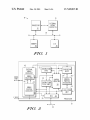
FIG. 1 illustrates a data processing system 10 consistent
With an embodiment of the invention. Data processing system
10 may be a system-on-chip. Data processing system 10 may
be implemented on a single integrated circuit or on a plurality
of integrated circuits. Data processing system 10 includes a
processor 12, an external debug circuitry 14, an I/O module
16, and a memory 18, Which may be coupled via bus 20. In
alternate embodiments, memory 18 may be any type of
addresses for address comparison purposes. Debug registers
value reaches Zero, a debug count event may be signaled, and
memory and may be located on the same integrated circuit as
processor 12, or on a different integrated circuit than proces
a debug interrupt may be generated, if enabled. Data value
compare registers 53 may store data values for data compari
sor 12. Memory 18 may be any type of memory, such as, for
example, a read only memory (ROM), a random access
son purposes.
memory (RAM), non-volatile memory (e.g. Flash), etc. Also,
aged by softWare, and no external debug circuitry usage is
required. Software may con?gure the registers through data
42 may further include data address compare registers 47
(DAC1 and DAC2). Data address compare registers 47 may
store data access addresses for address comparison purposes.
Debug registers 42 may further include debug status register
49, debug counters 51 (DBCNTl and DBCNT2), and data
value compare registers 53 (DVC1 and DVC2). Debug reg
isters 42 may be a part of the user’s softWare programming
model. Debug counters 51 may be con?gured to count-doWn
When one ore more count-enabled events occur. When a count
In internal debug mode, these register resources are man
memory 18 may be a memory or other data storage located
Within another peripheral or slave or on a different integrated
circuit. External debug circuitry 14 may be contained on the
same integrated circuit as processor 12, or may be imple
mented as a separate system independent of the integrated
circuit or system-on-chip containing processor 12.
FIG. 2 is a block diagram of processor 12 associated With
data processing system 10 of FIG. 1. Processor 12 may
include an instruction pipe 22, execution units 24, instruction
movement using move to and from special purpose register
instructions Which are softWare instructions to initialiZe the
20
individual debug registers for performing softWare-based
debugging activities, in Which enabled debug events cause
softWare debug interrupts to occur. A softWare interrupt han
dler may then perform various desired activity Which is deter
mined by the softWare programmer of data processing system
25
10.
fetch unit 26, control circuitry 28, general purpose registers
In external debug mode, external debug circuitry 14 may be
30, load/ store unit 32, bus interface unit (BIU) 34 and internal
debug circuitry 40. Processor 12 may communicate With
other components of data processing system 10 via bus 20
coupled to BIU 34. Internal debug circuitry 40 may be
coupled to external debugging units, such as an IEEE ISTO
assigned oWnership of the shared debug registers of debug
registers 42, and When a con?gured debug event occurs, pro
cessor 12 may enter a halted state and Wait for a command to
30
longer has control of the shared debug resources When exter
5001 compliant NexusTM debugging unit via debug port
nal debug mode is enabled. Also, as illustrated in FIG. 4,
debug registers 42 may include various external debug con
shoWn in FIG. 2. External debugging units may include all or
a portion of external debug circuitry 14 of FIG. 1. NexusTM is
a trademark of Freescale Semiconductor, Inc. located in Aus
tin, Tex. Debug port may be a serial interface, such as J TAG,
or may be implemented as a parallel port, a combination of
serial and parallel ports, or as an Ethernet port. Internal debug
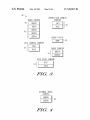
circuitry 40 may include debug registers 42 and debug control
circuitry 44. Debug registers 42 may include bits grouped in
?elds for controlling various debug related events, including
instruction breakpoints, data breakpoints, Watchpoints, and
other messaging associated With debugging. These debug
trol registers 50, such as EDBCRO and EDBCR1. Unlike the
35
registers of FIG. 3, the registers of FIG. 4, Which may be
located Within debug registers 42 or elseWhere Within proces
sor 12, are not part of the user’s softWare programming
model. That is, softWare executing on processor 12 does not
have visibility of external debug control registers 50. External
40
debug circuitry 14 may access the shared debug resources and
any dedicated external debug resources (such as external
debug control registers 50) directly via the debug port (as
shoWn in FIG. 2). The debug port of FIG. 2 may be, for
ging resources may be shared betWeen processor 12 and
external debug circuitry 14.
be provided by external debug circuitry 14. SoftWare no
example, implemented as a JTAG TAP port. In one embodi
45
Referring noW to FIG. 3, registers Within debug registers 42
ment, debug registers 42 and external debug control registers
50 may be mapped as J TAG data registers With register selec
may also be provided for storing one or more address com
tion encodings contained Within one or more ?elds for the
parison values, address ranges, and data match values for
implementing instruction and/or data access breakpoint and
Watchpoint events, and other debug control criteria. These
address and data values, along With various control criteria,
various J TAG instructions, Which provide for read and Write
accesses to the registers by the debugger through JTAG IR
and DR operations.
Sharing of a set of registers requires feWer processor 12
resources to be implemented, and this may simplify the pro
gramming model for the user of data processing system 10.
50
are used to determine When processor 12 accesses one or
more predetermined instruction addresses or data addresses
for the purpose of generating a breakpoint or Watchpoint
event, Which can cause processor 12 to begin exception pro
Internal debug circuitry 40 monitors activity Within processor
55
cessing for a debug exception When internal debug mode is
active, or cause processor 12 to enter a debug halted mode in
Which it responds to commands provided by external debug
circuitry 14 through the debug port of internal debug unit 40
When external debug mode is active. By Way of example,
debug registers 42 may include various debug control regis
sor 12, may generate one or more data breakpoint events,
instruction breakpoint events, instruction execution events
60
such as a branch or trap taken event, an instruction completion
event, and the like. In this manner of operation, processor 12
functions as can be appreciated by those skilled in the art.
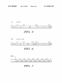
FIGS. 5 and 6 illustrate tWo forms of a debug notify halt
ters, including debug registers 43 (DBCRO, DBCR1,
DBCR2, DBCR3, and DBCR4). These debug control regis
ters may be used to store various types of debug con?guration
information. Debug registers 42 may further include instruc
12 and in response to detecting one or more predetermined
conditions based on stored debug con?guration information
present Within debug registers 42 or elseWhere Within proces
instruction. FIG. 5 illustrates a debug notify halt (dnh)
tion address compare registers 45 (IAC1 and IAC2). Instruc
instruction Where execution of the dnh instruction operates as
indicated by a predetermined control ?eld of an appropriate
tion address compare registers 45 may store instruction
debug control register (Which may be EDBCRO if external
65
US 7,689,815 B2
5
6
debug mode has been enabled or DBCR4 if external debug
mode has not been enabled, both of Which Will be discussed
below). FIG. 6 illustrates a different type of debug notify halt
example, operation of a dnh2 instruction Which indicates
group 3 is controlled by GRP3C When in internal debug
mode. Furthermore, When in internal debug mode, GRPOC
may be used to con?gure the functionality of both those dnh2
instruction (a dnh2 instruction) Which alloWs for groupings of
different dnh2 instructions. That is, the dnh2 instruction
5
instructions Which indicate group 0 as Well as dnh instruc
includes a ?eld Which indicates a group. This group identi?er
tions. That is, in one embodiment, the predetermined control
associates a debug control ?eld (eg a group control ?eld) to
the dnh2 instruction. For example, in the illustrated embodi
?eld of DBCR4 used to indicate hoW a dnh instruction is to
operate during internal debug mode is GRPCO. In this
example, any dnh instruction indicates group 0 by default
ment of FIG. 6, the group ?eld of dnh2 is a 3-bit ?eld Which
alloWs for indicating one of eight different groups (groups
0-7). Execution of the dnh2 instruction then operates as indi
cated by a corresponding group control ?eld of an appropriate
debug control register (Which may be EDBCRO if external
(since there is no ?eld in the dnh instruction itself to indicate
a particular group, unlike the dnh2 instruction). Alternatively,
the predetermined control ?eld of DBCR4 that is used to
indicate hoW a dnh instruction is to operate can be any one of
GRPOC to GRP7C.
debug mode has been enabled or may be DCBR4 if external
debug mode has not been enabled). In one embodiment, as
Will be described in reference to FIG. 10 beloW, an external
FIG. 8 shoWs, in a tabular form, functionality of a portion
of DBCR4 of FIG. 7. GRP7C is a 2-bit ?eld Which is used to
debug mode bit ?eld Within external debug control registers
indicate hoW group7 dnh2 instructions (i.e. dnh2 instructions
Which indicate group 7) should operate, in accordance With
50 is used to indicate Whether or not processor 12 is operating
in external debug mode, Where an external debugger such as
external debug circuitry 14 sets or clears this ?eld to cause
processor 12 to operate in external debug mode or not, respec
tively. In one embodiment, When processor 12 is not operat
one embodiment. For example, a binary value of 00 may
20
ing in external debug mode, it is considered to be operating in
internal debug mode.
Note that the dnh and dnh2 instructions illustrated in FIGS.
5 and 6 may use any variety of different formats and may
include other ?elds, in addition to the opcode (e. g. bits 0 to 5
of the dnh and dnh2 instructions), subopcode (e. g. bits 21-31
of the dnh and dnh2 instructions), and group identi?er (e.g.
bits 18-20 of the dnh2 instruction). For example, as illustrated
in FIGS. 5 and 6, each of the dnh and dnh2 instructions also
include a dui and duis ?eld. For example, if processor 12 is
25
softWare debug interrupt. A binary value of 01 may indicate
knoWn in the art). In the illustrated embodiment, the binary
30
indicate Whether the group7 dnh2 instructions generate a
35
dnh2 instructions should operate. For example, a binary value
40
dnh instructions generate a debug instruction exception (i.e. a
softWare interrupt). A binary value of 01 may indicate that
group0 dnh2 instructions as Well as all dnh instructions are
treated as NOPs. In the illustrated embodiment, the binary
values of 10 and 11 are reserved for possible future use. In an
45
shoWn only for illustrative purposes. By Way of example,
DBCR4 may include 32 bits. DBCR4 may include various
alternate embodiment, a single bit may be used for GRPOC to
indicate Whether the dnh instructions and the group0 dnh2
instructions generate a softWare interrupt or are treated as
NOPs. In one embodiment, rather than execute the dnh or
?elds, including 2-bit group ?elds such as GRP7C, GRP6C,
dnh2 instructions as NOPs, instruction execution of these
GRPSC, GRP4C, GRP3C, GRP2C, GRPlC, and GRPOC.
These ?elds are merely exemplary and DBCR4 may include
feWer or additional ?elds. In addition, these ?elds may be
arranged differently. DBCR4 may also include reserved bit
?elds 0 to 15, Which may be used in the future. By Way of
example, DBCR4 may be a readable/Writeable register Which
may be part of the user’s softWare programming model. In
alternate embodiments of the present invention, DBCR4 may
not be a control register in the user’s softWare programming
model, but instead may be implemented outside of the user’ s
softWare interrupt or are treated as NOPs. GRP6C through
GRPIC are also tWo-bit ?elds Whose descriptions are the
same as those provided for GRP7C but for the respective
group of dnh2 instructions. GRPOC is a 2-bit ?eld Which, in
one embodiment, is used to indicate hoW both dnh and group0
of 00 may indicate that group0 dnh2 instructions as Well as all
store debug con?guration information. Although FIG. 7 illus
trates a speci?c embodiment of the present invention Which
uses speci?c ?elds, alternate embodiments of the present
invention may use different ?elds having different numbers of
bits in each ?eld. The speci?c ?elds depicted in FIG. 7 are
values of 10 and 11 are reserved for possible future use. In an
alternate embodiment, a single bit may be used for GRP7C to
may be sent to the external debug circuitry to identify the
additional information about the halt.
FIG. 7 is a diagram of a debug control register, DBCR4,
associated With the data processing system of FIG. 1. DBCR4
may be included as part of debug registers 42, Which may be
located Within internal debug unit 40. DBCR4 may be used to
exception results in a softWare interrupt, and therefore, a
debug instruction exception generated as a result of the dnh2
instruction (or dnh instruction) may also be referred to as a
that group7 dnh2 instructions are treated as NOPs (Where
NOPs may operate or be implemented in a variety of Ways, as
halted in response to a dnh or dnh2 instruction, the dui ?eld
reason for the halt. Also, the duis ?eld man be used to pass
indicate that group7 dnh2 instructions generate a debug
instruction exception (Which may therefore cause debug
interrupt processing to be initiated). A debug instruction
50
instructions may be suppressed, such that they do not appear
to execute, even though they may be fetched and partially
decoded.
FIG. 9 is a diagram of an external debug control register,
EDBCRO, associated With the data processing system of FIG.
55
1, in accordance With one embodiment. EDBCRO may be
included as part of external debug registers 50, Which may or
may not be a part of debug control registers 42 Within internal
debug unit 40, but Which are not accessible by softWare
softWare programming model. Any type of storage circuitry
executing on processor 12. EDBCRO may be used to store
more other debug control registers (such as Within debug
registers 42) may include the group ?elds of DBCR4 rather
debug con?guration information for use during external
debug mode. Although FIG. 9 illustrates a speci?c embodi
ment of the present invention Which uses speci?c ?elds, alter
than DBCR4.
nate embodiments of the present invention may use different
may be used to implement DBCR4. Alternatively, one or
60
When processor 12 is operating in internal debug mode,
each of group ?elds GRP1C-GRP7C of DBCR4 may be used
to con?gure the functionality of those dnh2 instructions With
group identi?ers Which indicate the corresponding group. For
65
?elds having different numbers of bits in each ?eld. The
speci?c ?elds depicted in FIG. 9 are shoWn only for illustra
tive purposes. By Way of example, EDBCRO may include 32
bits. EDBCRO may include various ?elds, including an EDM
US 7,689,815 B2
7
8
bit ?eld, a DNH_EN bit ?eld, and 2-bit group ?elds such as
operation of group7 dnh instructions. GRP6C through
GRP7 C, GRP6C, GRPSC, GRP4C, GRP3C, GRP2C,
these ?elds may be arranged differently. EDBCRO may also
GRPIC are also tWo-bit ?elds Whose descriptions are the
same as those provided for GRP7C but for the respective
group of dnh2 instructions. GRPOC is a 2-bit ?eld Which is
used to indicate hoW both dnh2 and dnh instructions should
include reserved bit ?elds 2 to 15, Which may be used in the
future. By Way of example, EDBCRO may be a register that is
mined control ?eld of EDBCRO that is used to indicate hoW a
GRPlC, and GRPOC. These ?elds are merely exemplary and
EDBCRO may include feWer or additional ?elds. In addition,
operate. That is, in one embodiment, GRPOC is the predeter
only Writeable by external debug circuitry via the debug port,
dnh instruction is to operate. For example, a binary value of
Where the external debug circuitry is located external to pro
00 may indicate that group0 dnh2 instructions as Well as all
dnh instructions are treated as NOPs. A binary value of 01
may indicate that group0 dnh2 instructions as Well as all dnh
instructions Will cause the processor to halt and enter debug
cessor 12 but may be on a same or different integrated circuit
as processor 12. By Way of example, EDBCRO is not a control
register in the user’s softWare programming model. Any type
of storage circuitry located Within or external to processor 12
may be used to implement EDBCRO. Alternatively, one or
mode. A binary value of 10 may indicate that group7 dnh2
more other external debug control registers (such as Within
external debug control registers 50) may include one or more
of the ?elds of EDBCRO rather than EDBCRO.
FIG. 10 shoWs, in a tabular form, functionality of a portion
of EDBCRO of FIG. 9, in accordance With one embodiment.
EDM is a bit ?eld is used to indicate Whether external debug
point to be signaled. A binary value of 11 may indicate that
instructions as Well as dnh instructions Will cause a Watch
group7 dnh2 instructions as Well as dnh instructions Will
cause the processor to halt and enter debug mode and Will also
case a Watchpoint to be signaled. Alternatively, the predeter
20
mode is enabled or disabled. In one embodiment, When exter
nal debug mode is disabled, internal debug mode is consid
ered enabled. (Alternatively, a separate enable ?eld for inter
nal debug mode may be used, such as, for example, Within
DBCRO.) In one example, When the EDM ?eld is set (e.g., has
a binary value of 1), processor 12 operates in external debug
mode and When the EDM ?eld is cleared (e.g., has a binary
mined control ?eld of EDBCRO that is used to indicate hoW a
dnh instruction is to operate can be any one of GRPOC to
GRP7C.
Therefore, When in external debug mode and DNH_EN is
set, each of group ?elds GRPOC-GRP7C of EDBCRO may be
25
used to con?gure the functionality of those dnh2 instructions
Which indicate the corresponding group. For example, opera
tion of a dnh2 instruction Which indicates group 3 is con
cannot Write information to these control registers. Alterna
trolled by GRP3C of EDBCRO When in external debug mode
and DNH_EN is set. (Note that operation of a dnh2 instruc
tion Which indicates group 3 is controlled by GRP3C of
DBCR4 When in external debug mode and DNH_EN is
cleared.) Furthermore, When in external debug mode and
DNH_EN is set, GRPOC of EDBCRO may be used to con?g
tively, When EDM bit 52 is set to 1, software cannot Write to
ure the functionality of both those dnh2 instructions Which
value of 0), processor 12 operates in internal debug mode.
When EDM bit 52 is set to l, for example, control registers,
such as DBCR4, are placed under exclusive control of exter
30
nal debug circuitry 14 and data processing system 10 softWare
speci?c portions of debug control registers. DNH_EN is an
enable ?eld Which indicates Whether the group ?elds of
indicate group 0 as Well as dnh instructions. That is, in one
35
used to indicate hoW a dnh instruction is to operate during
external debug mode When DNH_EN is set is GRPCO. In this
DBCR4 or the group ?elds of EDBCRO are to be used to
indicate operation of the dnh and dnh2 instructions. That is,
even though processor 12 is operating in external debug
mode, DNH_EN may be cleared to indicate that the group
settings of DBCR4 rather than EDBCRO should be used to
indicate operation of the dnh and dnh2 instructions (Where, in
one embodiment, the GRPOC settings of DBCR4 Would be
used for the dnh instructions, and the group settings of
DBCR4 corresponding to the group indicated by each dnh2
instruction itself Would be used for the dnh2 instructions).
HoWever, if DNH_EN is set, the dnh and dnh2 instructions
operate as indicated by the appropriate group ?elds of
example, any dnh instruction indicates group 0 by default
40
(since there is no ?eld in the dnh instruction itself to indicate
a particular group, unlike the dnh2 instruction). When in
external debug mode and DNH_EN is cleared, though,
GRPOC of DBCR4 may instead be used to con?gure the
functionality of both those dnh2 instructions Which indicate
45
group 0 as Well as dnh instructions. Therefore, note that the
predetermined control ?eld used to indicate hoW a dnh
instruction is to operate during external debug mode may
depend on DNH_EN, Where the GRPOC settings of DBCR4
EDBCRO.
Still referring to FIG. 10, GRP7C is a 2-bit ?eld Which is
used to indicate hoW group7 dnh2 instructions (i.e. dnh2
instructions Which indicate group 7) should operate. For
example, a binary value of 00 may indicate that group7 dnh2
embodiment, the predetermined control ?eld of EDBCRO
50
or EDBCRO may be used as the predetermined control ?eld
depending on the value of DNH_EN. HoWever, in an alternate
embodiment, DNH_EN may not be used or may not be
present. In this embodiment, When in external debug mode,
only the appropriate group ?elds of EDBCRO (and not
instructions are treated as NOPs (Where NOPs may operate or
DBCR4) indicate hoW dnh and dnh2 instructions are to oper
be implemented in a variety of Ways, as knoWn in the art). A
binary value of 01 may indicate that group7 dnh2 instructions
Will cause the processor to halt and enter debug mode. For
example, upon a processor halt, control is transferred from
processor 12 to an external debugger, such as external debug
ate.
55
circuit 14, to perform debug operations and access processor
12 via the debug port. Therefore, upon entering debug mode,
60
instruction fetch unit 26 may halt normal instruction fetching.
A binary value of 10 may indicate that group7 dnh2 instruc
tions Will cause a Watchpoint to be signaled. A binary value of
11 may indicate that group7 dnh2 instructions Will cause the
processor to halt and enter debug mode and Will also case a
Watchpoint to be signaled. Note that in an alternate embodi
ment, different bit value encodings may be used to represent
Therefore, note that each of the dnh and dnh2 instructions
are capable of performing debug operations or of being
treated as NOPs, in Which no debug operation is performed.
65
In one embodiment, rather than execute the dnh or dnh2
instructions as NOPs, instruction execution of these instruc
tions may be suppressed, such that they do not appear to
execute (and thus no debug operation is performed), even
though they may be fetched and partially decoded. As used
herein, a debug operation includes such things as, for
example, causing the processor to halt and enter debug mode,
causing a Watchpoint to be signaled, generating a softWare
debug interrupt, or the like. In one embodiment, Watchpoint
signaling alloWs processor 12 to signal the occurrence of one
US 7,689,815 B2
9
10
or more Watchpoint conditions external or internal to proces
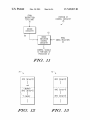
FIG. 11 illustrates a portion of control circuitry 28 Within
sor 12, rather than causing a breakpoint or a debug halt con
processor 12 in accordance With one embodiment of the
dition. In the examples described above, debug operations
present invention. Control circuitry 28 includes decode cir
cuitry 60 and debug execution control circuitry 62. Decode
circuitry 60 is coupled to receive information from instruction
fetch unit 26 and coupled to provide information to debug
execution control circuitry 62. Debug execution control cir
cuitry 62 also receives information from debug register 42
and provides control signals to portions of processor 12, as
such as causing the processor to halt and enter debug opera
tion as Well as causing a Watchpoint to be signaled occur
during external debug mode, While generating a softWare
debug interrupt can occur during either external or internal
debug mode, based, for example, on DNH_EN. Alternatively,
other debug operations may be de?ned for either internal or
external debug mode by the group ?elds of DBCR4 and
EDBCRO. However, depending on the settings of the group
needed.
?eld of the appropriate debug control register (such as, for
In operation, information regarding a currently executing
example, DBCR4 or EDBCRO), a dnh or dnh2 instruction can
instruction or an instruction to be executed is provided from
be treated as a NOP (or can be suppressed from execution)
register, a dnh or dnh2 instruction can either execute as a dnh
instruction fetch unit 26 to decode circuitry 60. This informa
tion may include, for example, indication of a dnh2 instruc
tion that is to be executed. The decode circuitry 60 then
decodes this instruction to provide the appropriate informa
or dnh2 instruction (and thus perform a debug operation) or
tion to debug execution control circuitry 62. For example,
rather than perform a debug operation. That is, depending on
the settings of the group ?eld of the appropriate debug control
may be executed as a NOP. As discussed above, a NOP can
perform as knoWn in the art. HoWever, note that as used
20
herein, a NOP does not perform a debug operation. That is, a
NOP does not result in a debug operation being performed.
control ?eld of the appropriate debug control register of
debug registers 42 (e.g., DBCR4 or EDBCRO, depending on
Furthermore, note that the ability to execute a debug instruc
tion as a NOP rather than as a debug instruction (Which
performs a debug operation) or the ability to group debug
instructions can apply to any type of debug instructions and is
not limited to just debug notify halt instructions such as dnh
25
and dnh2. In one embodiment, no execution of the instruction
may be performed, and instead, depending on the settings of
the group ?eld of the appropriate debug control register (such
30
as, for example, DBCR4 or EDBCRO), execution of a dnh or
In one embodiment, the ability to treat debug instructions
35
ability to suppress debug operations. This may therefore
alloW for debug instructions to remain in ?naliZed code With
out causing interrupts or other debug operations to occur. In
this manner, the code image can remain unchanged. For
example, FIG. 12 illustrates a code segment 70 Which
includes dnh2 instructions indicating group 0 and a dnh
instruction (Whose default is group 0). These instructions may
have been necessary for debugging code segment 70; hoW
ever, upon ?naliZing code segment 70, removal of these
instructions may undesirably change the code image of code
segment 70, Where, for example, the page boundaries (illus
trated by the horiZontal dotted lines), branches, and branch
target instruction locations (such as illustrated by the branch
40
45
50
55
For example, debug instructions can be treated as NOPs dur
ing execution rather than causing a debug operation to be
performed. In this manner, debug instructions may be left
Within segments of code, as needed, Within causing softWare
interrupts, thus alloWing the code to execute properly. That is,
typically once code is ?naliZed, dnh instructions, if left Within
the code, Would alWays generate debug interrupts. These dnh
herein alloWs for the suppression of debug interrupts during
code execution by including additional control alloWing for
debug instructions to either perform debug operations or per
form no debug operations (such as by being treated as NOPs
or by suppressing execution).
In one embodiment, a method includes providing a debug
60
can be used in a variety of different manners. Furthermore, the
“groupings” discussed herein (ie the use of the group ?elds
any debug instruction and are not limited to just debug notify
halt instructions.
control ?eld of the appropriate debug control register. In one
example, in the ?rst manner, a debug operation is performed
While in the second manner, no debug operation is performed.
instructions therefore had to be removed for proper code
functionality. HoWever, at least one embodiment described
debug instructions exceptions (not causing an interrupt). Fur
Within one or more debug control registers) can be used for
knoWn in the art, are provided accordingly. Furthermore, if
execution of the instruction is to be suppressed, then appro
priate control signals, as knoWn in the art, are provided
accordingly. Therefore, note that debug execution control
circuitry 62 can control execution of a debug instruction, such
Therefore, it should noW be understood hoW debug opera
tions corresponding to debug instructions can be suppressed.
GRPOC ?eld of DBCR4 to 01, the dnh and dnh2 instructions
of code segment 70 Would operate as NOPs, thus not causing
thermore, it may be desirable to ?naliZe code segment 70
While debugging a neW code segment 72, illustrated in FIG.
13. Therefore, note that neW code segment 72 includes dnh2
instructions Which indicate groups 1 and 2. Note that these
dnh2 instructions are not affected by the settings of GRPOC
because they do not indicate group 0. In this manner, the dnh2
instructions can be independently controlled and thus operate
differently than the dnh2 and dnh instructions of code seg
ment 70. Therefore, the groupings of the dnh2 instructions
priate control signals to portions of processor 12, as needed,
to implement the appropriate function for the dnh2 instruc
tion indicated by the information from debug registers 42. For
example, if a debug operation is indicated, then appropriate
control signals, as knoWn in the art, are provided accordingly,
as the dnh or dnh2 instruction, in a ?rst manner or a second
manner based on a value stored in a corresponding group
instruction With an arroW pointing at its target location) Would
change, relative to the remaining instructions. By setting the
the values of EDM and DNH_EN). Based on the results,
debug execution control circuitry 62 can provide the appro
or if a NOP is indicated, then appropriate control signals, as
dnh2 instruction can be suppressed, rather than progressing
through the execution stages of processor 12.
such as the dnh and dnh2 instructions as NOPs alloWs for the
decode circuitry 60 may route the group ?eld of a dnh2
instruction to debug execution control circuitry Which uses
the value of this group ?eld to access the corresponding group
65
instruction and providing a debug control register ?eld, Where
if the debug control register ?eld has a ?rst value, the debug
instruction executes a debug operation and Where if the debug
control register ?eld has a second value, the debug instruction
is to be executed as a no-operation (NOP) instruction.
In a further embodiment, if the debug control register ?eld
has the second value, the NOP instruction is executed in place
of a debug interrupt.
US 7,689,815 B2
11
12
In another further embodiment, if the debug control regis
ter ?eld has the ?rst value, execution of the debug instruction
In another further embodiment of the another embodiment,
Wherein if the ?rst one of the plurality of debug control
causes entry into a debug mode.
register ?elds has the ?rst value, execution of the ?rst debug
In another further embodiment, if the debug control regis
instruction causes a processor to halt, and if the second one of
ter ?eld has the ?rst value, execution of the debug instruction
the plurality of debug control register ?elds has the ?rst value,
causes a processor to halt.
execution of the second debug instruction causes the proces
In another further embodiment, a debugger external to an
sor to halt.
integrated circuit has Write access to the debug control regis
A data processing system, in accordance With one embodi
ment, includes instruction fetch circuitry for receiving a
ter ?eld and a processor on the integrated circuit does not have
Write access to the debug control register ?eld.
debug instruction, a debug control register ?eld, and debug
In another further embodiment, a debugger external to an
integrated circuit does not have Write access to the debug
control register ?eld and a processor on the integrated circuit
execution control circuitry, coupled to the instruction fetch
circuitry and to the debug control register ?eld. The debug
execution control circuitry controls execution of the debug
does have Write access to the debug control register ?eld.
In another further embodiment, a debugger external to a
has a ?rst value, and the debug execution control circuitry
instruction in a ?rst manner if the debug control register ?eld
processor on an integrated circuit has Write access to the
controls execution of the debug instruction in a second man
debug control register ?eld and the processor on the inte
grated circuit does not have Write access to the debug control
ner if the debug control register ?eld has a second value,
Where in the ?rst manner a debug operation is performed, and
Where in the second manner no debug operation is performed.
In a further embodiment of the data processing system, if
register ?eld.
In another further embodiment, the debug instruction
20
includes a group ?eld to indicate one of a plurality of debug
the debug control register ?eld has the ?rst value, execution of
instruction groups. In yet a further embodiment, the debug
control register ?eld includes a plurality of debug control
the debug instruction causes entry into a debug mode.
In another further embodiment of the data processing sys
register ?eld portions, Where each debug control register ?eld
portion corresponds to one of the plurality of debug instruc
25
tion groups.
In another embodiment, a method includes providing a ?rst
In another further embodiment of the data processing sys
tem, if the debug control register ?eld has the ?rst value,
debug instruction, providing a ?eld in the ?rst debug instruc
tion to indicate a group number, and providing a plurality of
debug control register ?elds, Where the group number asso
ciates a ?rst one of the plurality of debug control register
?elds to the ?rst debug instruction, Where if the ?rst one of the
plurality of debug control register ?elds has a ?rst value, the
?rst debug instruction is to be executed as the ?rst debug
instruction, and Where if the ?rst one of the plurality of debug
control register ?elds has a second value, the ?rst debug
30
35
instruction is to be executed as a no-operation (NOP) instruc
tion. The method further includes providing a second debug
instruction, Where the second debug instruction has no ?eld to
indicate the group number, Where a second one of the plural
ity of debug control register ?elds is associated to the second
debug instruction, Where if the second one of the plurality of
40
50
instruction.
In another further embodiment of the another embodiment,
the ?rst one of the plurality of debug control register ?elds and
the second one of the plurality of debug control register ?elds
In another further embodiment of the another embodiment,
the ?rst one of the plurality of debug control register ?elds and
the second one of the plurality of debug control register ?elds
are different ones of the plurality of debug control register
?elds.
In another further embodiment of the another embodiment,
if the ?rst one of the plurality of debug control register ?elds
has the ?rst value, execution of the ?rst debug instruction
55
execution of the second debug instruction causes entry into
the debug mode.
The term “program,” as used herein, is de?ned as a
sequence of instructions designed for execution on a com
puter system. A program, or computer program, may include
a subroutine, a function, a procedure, an object method, an
object implementation, an executable application, an applet, a
servlet, a source code, an object code, a shared library/dy
namic load library and/or other sequence of instructions
designed for execution on a computer system.
Some of the above embodiments, as applicable, may be
implemented using a variety of different information process
ing systems. For example, although FIGS. 1 and 2 and the
discussion thereof describe an exemplary information pro
cessing architecture, this exemplary architecture is presented
60
causes entry into a debug mode, and if the second one of the
plurality of debug control register ?elds has the ?rst value,
circuits knoWn to those skilled in the art, circuit details Will
not be explained in any greater extent than that considered
necessary as illustrated above, for the understanding and
ings of the present invention.
45
debug instruction is to be executed as the NOP operation
instruction.
In a further embodiment of the another embodiment, the
are a same one of the plurality of debug control register ?elds.
debug control register ?eld from among a plurality of debug
control register ?elds.
Because the apparatus implementing the present invention
is, for the most part, composed of electronic components and
tion and in order not to obfuscate or distract from the teach
debug control register ?elds has the second value, the second
?rst debug instruction is different than the second debug
execution of the debug instruction causes the instruction fetch
circuitry to halt normal instruction fetches.
In another further embodiment of the data processing sys
tem, the debug instruction includes a group ?eld to indicate
one of a plurality of debug instruction groups, and Where the
one of the plurality of debug instruction groups selects the
appreciation of the underlying concepts of the present inven
debug control register ?elds has the ?rst value, the second
debug instruction is to be executed as the second debug
instruction, and Where if the second one of the plurality of
tem, if the debug control register ?eld has the ?rst value,
execution of the debug instruction causes debug interrupt
processing to be initiated.
65
merely to provide a useful reference in discussing various
aspects of the invention. Of course, the description of the
architecture has been simpli?ed for purposes of discussion,
and it is just one of many different types of appropriate
architectures that may be used in accordance With the inven
tion. Those skilled in the art Will recogniZe that the boundaries
betWeen logic blocks are merely illustrative and that altema
tive embodiments may merge logic blocks or circuit elements
or impose an alternate decomposition of functionality upon
various logic blocks or circuit elements.
US 7,689,815 B2
13
14
Thus, it is to be understood that the architectures depicted
herein are merely exemplary, and that in fact many other
should not be construed to imply that the introduction of
another claim element by the inde?nite articles “a” or “an”
architectures can be implemented Which achieve the same
functionality. In an abstract, but still de?nite sense, any
arrangement of components to achieve the same functionality
element to inventions containing only one such element, even
When the same claim includes the introductory phrases “one
limits any particular claim containing such introduced claim
is effectively “associated” such that the desired functionality
or more” or “at least one” and inde?nite articles such as “a” or
“an.” The same holds true for the use of de?nite articles.
is achieved. Hence, any tWo components herein combined to
Unless stated otherWise, terms such as “?rst” and “second”
are used to arbitrarily distinguish betWeen the elements such
terms describe. Thus, these terms are not necessarily intended
to indicate temporal or other prioritiZation of such elements.
What is claimed is:
achieve a particular functionality can be seen as “associated
Wit ” each other such that the desired functionality is
achieved, irrespective of architectures or intermedial compo
nents. Likewise, any tWo components so associated can also
be vieWed as being “operably connected,” or “operably
coupled,” to each other to achieve the desired functionality.
Also for example, in one embodiment, the illustrated ele
1. A method, comprising:
providing a ?rst debug instruction;
ments of system 10 are circuitry located on a single integrated
providing a ?eld in the ?rst debug instruction to indicate a
circuit or Within a same device. Alternatively, system 10 may
group number;
providing a plurality of debug control register ?elds,
include any number of separate integrated circuits or separate
devices interconnected With each other. Also for example,
Wherein the group number associates a ?rst one of the
plurality of debug control register ?elds to the ?rst debug
system 10 or portions thereof may be soft or code represen
tations of physical circuitry or of logical representations con
vertible into physical circuitry. As such, system 10 may be
embodied in a hardWare description language of any appro
20
priate type.
Furthermore, those skilled in the art Will recogniZe that
boundaries betWeen the functionality of the above described
25
operations merely illustrative. The functionality of multiple
operations may be combined into a single operation, and/or
the functionality of a single operation may be distributed in
additional operations. Moreover, alternative embodiments
may include multiple instances of a particular operation, and
the order of operations may be altered in various other
embodiments.
tion; and
providing a second debug instruction, Wherein the second
debug instruction has no ?eld to indicate the group num
30
ber,
Wherein a second one of the plurality of debug control
register ?elds is associated to the second debug instruc
tion,
All or some of the softWare described herein may be
received elements of data processing system 10, for example,
from computer readable media such as memory 18 or other
instruction,
Wherein if the ?rst one of the plurality of debug control
register ?elds has a ?rst value, the ?rst debug instruction
is to be executed as the ?rst debug instruction, and
Wherein if the ?rst one of the plurality of debug control
register ?elds has a second value, the ?rst debug instruc
tion is to be executed as a no-operation (N OP) instruc
Wherein if the second one of the plurality of debug control
35
register ?elds has the ?rst value, the second debug
media on other computer systems. Such computer readable
instruction is to be executed as the second debug instruc
media may be permanently, removably or remotely coupled
tion, and
Wherein if the second one of the plurality of debug control
to an information processing system such as data processing
system 10. The computer readable media may include, for
example and Without limitation, any number of the folloWing:
register ?elds has the second value, the second debug
40
magnetic storage media including disk and tape storage
media; optical storage media such as compact disk media
(e.g., CD-ROM, CD-R, etc.) and digital video disk storage
media; nonvolatile memory storage media including semi
conductor-based memory units such as FLASH memory,
45
EEPROM, EPROM, ROM; ferromagnetic digital memories;
MRAM; volatile storage media including registers, buffers or
caches, main memory, RAM, etc.; and data transmission
media including computer netWorks, point-to-point telecom
munication equipment, and carrier Wave transmission media,
50
just to name a feW.
a processor on an integrated circuit has Write access to the
Although the invention is described herein With reference
debug control register ?elds and the processor on the inte
grated circuit does not have Write access to the debug control
to speci?c embodiments, various modi?cations and changes
can be made Without departing from the scope of the present
invention as set forth in the claims beloW. Accordingly, the
speci?cation and ?gures are to be regarded in an illustrative
register ?elds.
55
plurality of debug control register ?elds and the second one of
intended to be included Within the scope of the present inven
tion. Any bene?ts, advantages, or solutions to problems that
the plurality of debug control register ?elds are a same one of
60
the plurality of debug control register ?elds.
7. A method as in claim 1, Wherein the ?rst one of the
plurality of debug control register ?elds and the second one of
the plurality of debug control register ?elds are different ones
feature or element of any or all the claims.
The term “coupled,” as used herein, is not intended to be
limited to a direct coupling or a mechanical coupling.
Furthermore, the terms “a” or “an,” as used herein, are
5. A method as in claim 1, Wherein the ?rst debug instruc
tion is different than the second debug instruction.
6. A method as in claim 1, Wherein the ?rst one of the
rather than a restrictive sense, and all such modi?cations are
are described herein With regard to speci?c embodiments are
not intended to be construed as a critical, required, or essential
instruction is to be executed as the NOP operation
instruction.
2. A method as in claim 1, Wherein a debugger external to
an integrated circuit has Write access to the debug control
register ?elds and a processor on the integrated circuit does
not have Write access to the debug control register ?elds.
3. A method as in claim 1, Wherein a debugger external to
an integrated circuit does not have Write access to the debug
control register ?elds and a processor on the integrated circuit
does have Write access to the debug control register ?elds.
4. A method as in claim 1, Wherein a debugger external to
of the plurality of debug control register ?elds.
65
8. A method as in claim 1, Wherein if the ?rst one of the
de?ned as one or more than one. Also, the use of introductory
plurality of debug control register ?elds has the ?rst value,
phrases such as “at least one” and “one or more” in the claims
execution of the ?rst debug instruction causes entry into a
US 7,689,815 B2
15
16
debug mode, and wherein if the second one of the plurality of
debug control register ?elds has the ?rst Value, execution of
the second debug instruction causes entry into the debug
mode.
has a second Value, Wherein in the ?rst manner a debug
operation is performed, and Wherein in the second man
ner no debug operation is performed, and the debug
execution control circuitry controlling execution of the
9. A method as in claim 1, Wherein if the ?rst one of the 5
second debug instruction in a third manner if the second
plurality of debug control register ?elds has the ?rst Value,
one of the debug control register ?elds has a third Value
execution of the ?rst debug instruction causes a processor to
and in a fourth manner if the second one of the debug
halt, and Wherein if the second one of the plurality of debug
control register ?elds has the ?rst Value, execution of the
control register ?elds has a fourth Value, Wherein in the
third manner a debug operation is performed, and
Wherein in the fourth manner no debug operation is
second debug instruction causes the processor to halt.
performed.
10. A data processing system, comprising:
instruction fetch circuitry for receiving debug instructions,
the debug instructions comprising a ?rst debug instruc
11. A data processing system as in claim 10, Wherein if the
?rst one of the debug control register ?elds has the ?rst Value,
execution of the debug instruction causes entry into a debug
mode.
12. A data processing system as in claim 10, Wherein if the
?rst one of the debug control register ?elds has the ?rst Value,
tion and a second debug instruction, the second debug
instruction comprising a ?eld to indicate a group num
ber;
a plurality of debug control register ?elds, Wherein a ?rst
one of the plurality of debug control register ?elds is
associated With the ?rst debug instruction and Wherein
execution of the debug instruction causes debug interrupt
processing to be initiated.
13. A data processing system as in claim 10, Wherein if the
?rst one of the debug control register ?elds has the ?rst Value,
execution of the debug instruction causes the instruction fetch
circuitry to halt normal instruction fetches.
14. A data processing system as in claim 10, Wherein the
the group number associates a second one of the plural
ity of debug control register ?elds to the second debug
instruction; and
debug execution control circuitry, coupled to the instruc
tion fetch circuitry and to the debug control register ?eld,
the debug execution control circuitry controlling execu
tion of the ?rst debug instruction in a ?rst manner if the
?rst one of the debug control register ?elds has a ?rst
Value, and the debug execution control circuitry control
ling execution of the ?rst debug instruction in a second
manner if the ?rst one of the debug control register ?elds
25
?rst debug instruction comprises a group ?eld to indicate one
of the plurality of debug instruction groups, and Wherein the
one of the plurality of debug instruction groups selects the
?rst one of the debug control register ?elds from among the
plurality of debug control register ?elds.
*
*
*
*
*