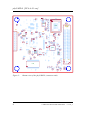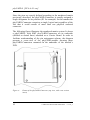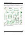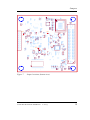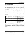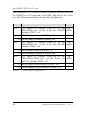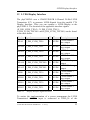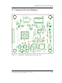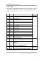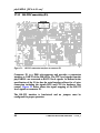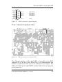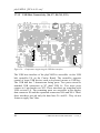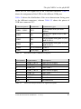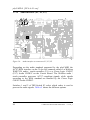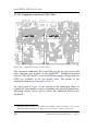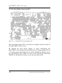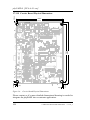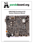
1
phyCARD-L Hardware Manual Document No.: L-751e_1 SBC Prod. No.: PCA-A-L1-xxx SBC PCB. No.: 1334.2 CB Prod. No.: CB PCB. No.: Edition: PBA-A-01 1333.2 December 2010 A product of a PHYTEC Technology Holding company phyCARD-L [PCA-A-L1-xxx] In this manual are descriptions for copyrighted products that are not explicitly indicated as such. The absence of the trademark (™) and copyright (©) symbols does not imply that a product is not protected. Additionally, registered patents and trademarks are similarly not expressly indicated in this manual. The information in this document has been carefully checked and is believed to be entirely reliable. However, PHYTEC Messtechnik GmbH assumes no responsibility for any inaccuracies. PHYTEC Messtechnik GmbH neither gives any guarantee nor accepts any liability whatsoever for consequential damages resulting from the use of this manual or its associated product. PHYTEC Messtechnik GmbH reserves the right to alter the information contained herein without prior notification and accepts no responsibility for any damages which might result. Additionally, PHYTEC Messtechnik GmbH offers no guarantee nor accepts any liability for damages arising from the improper usage or improper installation of the hardware or software. PHYTEC Messtechnik GmbH further reserves the right to alter the layout and/or design of the hardware without prior notification and accepts no liability for doing so. © Copyright 2010 PHYTEC Messtechnik GmbH, D-55129 Mainz. Rights - including those of translation, reprint, broadcast, photomechanical or similar reproduction and storage or processing in computer systems, in whole or in part - are reserved. No reproduction may occur without the express written consent from PHYTEC Messtechnik GmbH. Address: EUROPE NORTH AMERICA PHYTEC Technologie Holding AG Robert-Koch-Str. 39 D-55129 Mainz GERMANY PHYTEC America LLC 203 Parfitt Way SW, Suite G100 Bainbridge Island, WA 98110 USA +49 (800) 0749832 Ordering Information: [email protected] 1 (800) 278-9913 [email protected] Technical Support: +49 (6131) 9221-31 [email protected] 1 (800) 278-9913 [email protected] Fax: +49 (6131) 9221-33 1 (206) 780-9135 Web Site: http://www.phytec.de http://www.phytec.com 1st Edition December 2010 © PHYTEC Messtechnik GmbH 2010 L-751e_1 Contents List of Figures..............................................................................................iii List of Tables ...............................................................................................iv Conventions, Abbreviations and Acronyms............................................vii Preface..........................................................................................................ix 1 Introduction......................................................................................... 1 1.1 Block Diagram ............................................................................. 4 1.2 View of the phyCARD-L ............................................................. 5 1.3 Minimum Requirements to Operate the phyCARD-L ................. 7 2 Pin Description .................................................................................... 9 3 Jumpers.............................................................................................. 17 4 Power.................................................................................................. 23 4.1 Primary System Power (VDD_3V3).......................................... 23 4.2 Standby Voltage (VSTBY) ........................................................ 24 4.3 On-board Voltage Regulator (U1).............................................. 24 4.4 Supply Voltage for external Logic ............................................. 26 5 Power Management .......................................................................... 27 6 System Configuration and Booting ................................................. 29 7 System Memory................................................................................. 31 7.1 LP-DDR-SDRAM and NAND Flash......................................... 31 7.2 I²C EEPROM (U10)................................................................... 32 7.2.1 Setting the EEPROM Lower Address Bits (J3, J2, J1). 33 7.2.2 EEPROM Write Protection Control (J5) ...................... 34 7.3 Memory Model........................................................................... 34 8 SD / MMC Card Interfaces .............................................................. 35 9 Serial Interfaces................................................................................. 37 9.1 Universal Asynchronous Interface ............................................. 38 9.2 USB-OTG Transceiver (U16) .................................................... 39 9.3 USB-Host Transceiver (U15)..................................................... 40 9.4 Ethernet Interface ....................................................................... 41 9.4.1 Ethernet Controller (U12) ............................................. 41 9.4.2 Software Reset of the Ethernet Controller (J10)........... 43 9.4.3 MAC Address................................................................ 43 9.5 I2C Interface ............................................................................... 44 9.6 SPI Interface ............................................................................... 44 9.7 Synchronous Serial Interface (SSI) ............................................ 45 10 General Purpose I/Os........................................................................ 47 11 Debug Interface (X1) ........................................................................ 49 © PHYTEC Messtechnik GmbH 2010 L-751e_1 i phyCARD-L [PCA-A-L1-xxx] 12 13 14 15 16 17 LVDS Display Interface ................................................................... 53 12.1 Signal configuration (J7)............................................................ 54 12.2 LVDS Display Interface pixel mapping .................................... 54 LVDS Camera Interface .................................................................. 57 13.1 Signal configuration (J6)............................................................ 58 Technical Specifications ................................................................... 59 Component Placement Diagram ..................................................... 63 Hints for Integrating and Handling the phyCARD-L................... 65 16.1 Integrating the phyCARD-M ..................................................... 65 16.2 Handling the phyCARD-L ......................................................... 67 The phyCARD-L on the phyBASE ................................................. 69 17.1 Concept of the phyBASE Board ................................................ 70 17.2 Overview of the phyBASE Peripherals ..................................... 71 17.2.1 Connectors and Pin Header........................................... 72 17.2.2 Switches ........................................................................ 73 17.2.3 LEDs ............................................................................. 76 17.2.4 Jumpers ......................................................................... 77 17.3 Functional Components on the phyBASE Board ...................... 80 17.3.1 phyCARD-L SBC Connectivity (X27)......................... 80 17.3.2 Power Supply (X28) ..................................................... 81 17.3.3 RS-232 Connectivity (P1)............................................. 84 17.3.4 Ethernet Connectivity (X10)......................................... 85 17.3.5 USB Host Connectivity (X6, X7, X8, X9, X33) .......... 86 17.3.6 USB OTG Connectivity (X29) ..................................... 88 17.3.7 Display / Touch Connectivity (X6, X32)...................... 89 17.3.7.1 Display Data Connector (X6) ........................ 90 17.3.7.2 Display Power Connector (X32) ................... 92 17.3.7.3 Touch Screen Connectivity ........................... 93 17.3.8 Camera Interface (X5) .................................................. 95 17.3.9 Audio Interface (X1, X2, X3) ....................................... 96 17.3.10 I2C Connectivity............................................................ 98 17.3.11 SPI Connectivity ........................................................... 99 17.3.12 User programmable GPIOs........................................... 99 17.3.13 Expansion connectors (X8A, X9A) ............................ 100 17.3.14 Secure Digital Memory Card/ MultiMedia Card (X26) ..................................................................................... 103 17.3.15 Boot Mode Selection (JP1) ......................................... 104 17.3.16 System Reset Button (S1) ........................................... 105 17.3.17 RTC at U3 ................................................................... 106 17.3.18 PLD at U25 ................................................................. 107 © PHYTEC Messtechnik GmbH 2010 L-751e_1 Contents 17.3.19 Carrier Board Physical Dimensions ............................ 108 18 Revision History .............................................................................. 109 Index.......................................................................................................... 111 List of Figures Figure 1: Block Diagram of the phyCARD-L ........................................... 4 Figure 2: Top view of the phyCARD-L (controller side).......................... 5 Figure 3: Bottom view of the phyCARD-L (connector side).................... 6 Figure 4: Pinout of the phyCARD-Connector (top view, with cross section insert) ........................................................................... 10 Figure 5: Typical jumper pad numbering scheme ................................... 17 Figure 6: Jumper locations (top view)..................................................... 18 Figure 7: Jumper locations (bottom view)............................................... 19 Figure 8: Power Supply Diagram ............................................................ 25 Figure 9: JTAG interface at X1 (top view).............................................. 49 Figure 10: JTAG interface at X1 (bottom view) ....................................... 50 Figure 11: Physical dimensions ................................................................. 59 Figure 12: phyCARD-L component placement (top view) ....................... 63 Figure 13: phyCARD-L component placement (bottom view)................. 64 Figure 14: Footprint of the phyCARD-L................................................... 66 Figure 15: phyBASE Overview of Connectors, LEDs and Buttons ......... 71 Figure 16: Typical jumper numbering scheme.......................................... 77 Figure 17: phyBASE jumper locations...................................................... 78 Figure 18: phyCARD-L SBC Connectivity to the Carrier Board ............. 80 Figure 19: Power adapter........................................................................... 81 Figure 20: Connecting the Supply Voltage at X28.................................... 82 Figure 21: RS-232 connection interface at connector P1 .......................... 84 Figure 22: RS232 connector P1 signal mapping ....................................... 85 Figure 23: Ethernet interface at connector X10......................................... 85 Figure 24: Components supporting the USB host interface ...................... 86 © PHYTEC Messtechnik GmbH 2010 L-751e_1 iii phyCARD-L [PCA-A-L1-xxx] Figure 25: USB OTG interface at connector X29..................................... 88 Figure 26: Universal LVDS interface at connector X6............................. 89 Figure 27: Camera interface at connectors X5.......................................... 95 Figure 28: Audio interface at connectors X1, X2, X3 .............................. 96 Figure 29: Expansion connector X8A, X9A ........................................... 100 Figure 30: SD / MM Card interface at connector X26............................ 103 Figure 31: Boot Mode Selection Jumper JP1.......................................... 104 Figure 32: System Reset Button S1......................................................... 105 Figure 33: RTC with Battery Buffer ....................................................... 106 Figure 34: Carrier Board Physical Dimensions....................................... 108 List of Tables Table 1: Abbreviations and Acronyms used in this Manual................. viii Table 2: X-Arc Bus pinout..................................................................... 12 Table 3: Pinout of the phyCARD-Connector X2................................... 16 Table 4: Jumper settings ........................................................................ 21 Table 5: Power Management Pins ......................................................... 27 Table 6: Power States............................................................................. 28 Table 7: Boot Modes of OMAP35x module.......................................... 30 Table 8: Compatible NAND Flash devices............................................ 32 Table 9: U10 EEPROM I²C address via J1, J2, and J3.......................... 33 Table 10: EEPROM write protection states via J5 .................................. 34 Table 11: Location of SD/ MMC Card interface signals......................... 35 Table 12: Location of the UART signals ................................................. 38 Table 13: Location of the USB-OTG signals........................................... 39 Table 14: Location of the USB-Host signals ........................................... 40 Table 15: Location of the Ethernet signals .............................................. 41 Table 16: Software Reset of the Ethernet Controller .............................. 43 Table 17: I2C Interface Signal Location .................................................. 44 © PHYTEC Messtechnik GmbH 2010 L-751e_1 Contents Table 18: SPI Interface Signal Location .................................................. 45 Table 19: SSI Interface Signal Location .................................................. 46 Table 20: Location of GPIO and IRQ pins .............................................. 47 Table 21: Possible GPIO configurations.................................................. 48 Table 22: JTAG connector X1 signal assignment.................................... 51 Table 23: Display Interface Signal Location............................................ 53 Table 24: Pixel mapping of 18-bit LVDS display interface .................... 54 Table 25: Pixel mapping of 24-bit LVDS display interface .................... 55 Table 26: Camera Interface Signal Location............................................ 57 Table 27: LVDS signal configuration J6.................................................. 58 Table 28: phyBASE Connectors and Pin Headers ................................... 72 Table 29: phyBASE push buttons descriptions........................................ 73 Table 30: phyBASE DIP-Switch S3 descriptions .................................... 75 Table 31: phyBASE LEDs descriptions................................................... 76 Table 32: phyBASE jumper descriptions................................................. 79 Table 33: LEDs assembled on the Carrier Board..................................... 82 Table 34: Distribution of the USB hub's (U4) ports ................................ 87 Table 35: Universal USB pin header X33 signal description .................. 87 Table 36: Display data connector signal description ............................... 91 Table 37: SPI and GPIO connector selection........................................... 92 Table 38: LVDS power connector X32 signal description ...................... 92 Table 39: Selection of the touch screen controller................................... 94 Table 40: PHYTEC camera connector X5............................................... 95 Table 41: Selection of the audio codec .................................................... 97 Table 42: I2C connectivity........................................................................ 98 Table 43: I2C addresses in use.................................................................. 98 Table 44: SPI connector selection ............................................................ 99 Table 45: SPI and GPIO connector selection......................................... 101 Table 46: PHYTEC expansion connector X8A, X9A............................ 102 © PHYTEC Messtechnik GmbH 2010 L-751e_1 v phyCARD-L [PCA-A-L1-xxx] © PHYTEC Messtechnik GmbH 2010 L-751e_1 Conventions, Abbreviations and Acronyms Conventions, Abbreviations and Acronyms This hardware manual describes the PCA-A-L1 Single Board Computer in the following referred to as phyCARD-L. The manual specifies the phyCARD-L's design and function. Precise specifications for the Texas Instruments OMAP35x microcontrollers can be found in the enclosed microcontroller Data Sheet/User's Manual. Conventions The conventions used in this manual are as follows: Signals that are preceded by a "n", "/", or “#”character (e.g.: nRD, /RD, or #RD), or that have a dash on top of the signal name (e.g.: RD) are designated as active low signals. That is, their active state is when they are driven low, or are driving low. A "0" indicates a logic zero or low-level signal, while a "1" represents a logic one or high-level signal. Tables which describe jumper settings show the default position in bold, blue text. Text in blue italic indicates a hyperlink within, or external to the document. Click these links to quickly jump to the applicable URL, part, chapter, table, or figure. References made to the phyCARD-Connector always refer to the high density molex connector on the undersides of the phyCARD-L Single Board Computer. Abbreviations and Acronyms Many acronyms and abbreviations are used throughout this manual. Use the table below to navigate unfamiliar terms used in this document. Abbreviation BSP CB Definition Board Support Package (Software delivered with the Development Kit including an operating system (Windows, or Linux) preinstalled on the module and Development Tools). Carrier Board; used in reference to the phyBASE Development Kit Carrier Board. © PHYTEC Messtechnik GmbH 2010 L-751e_1 vii phyCARD-L [PCA-A-L1-xxx] Abbreviation DFF EMB EMI GPI GPIO GPO IRAM J JP PCB PEB POR RTC SBC SMT Sx Sx_y VSTBY Table 1: Definition D flip-flop. External memory bus. Electromagnetic Interference. General purpose input. General purpose input and output. General purpose output. Internal RAM; the internal static RAM on the Texas Instruments OMAP35x microcontroller. Solder jumper; these types of jumpers require solder equipment to remove and place. Solderless jumper; these types of jumpers can be removed and placed by hand with no special tools. Printed circuit board. PHYTEC Extension Board Power-on reset Real-time clock. Single Board Computer; used in reference to the PCA-A-L1 /phyCARD-A-L1 Single Board Computer Surface mount technology. User button Sx (e.g. S1, S2, etc.) used in reference to the available user buttons, or DIP-Switches on the Carrier Board. Switch y of DIP-Switch Sx; used in reference to the DIP-Switch on the Carrier Board. SBC standby voltage input Abbreviations and Acronyms used in this Manual Note: The BSP delivered with the phyCARD-L usually includes drivers and/or software for controlling all components such as interfaces, memory, etc.. Therefore programming close to hardware at register level is not necessary in most cases. For this reason, this manual contains no detailed description of the controller's registers, or information relevant for software development. Please refer to the OMAP35x Reference Manual, if such information is needed to connect customer designed applications. viii © PHYTEC Messtechnik GmbH 2010 L-751e_1 Preface Preface As a member of PHYTEC's new phyCARD product family the phyCARD-L is one of a series of PHYTEC Single Board Computers (SBCs) that can be populated with different controllers and, hence, offers various functions and configurations. PHYTEC supports a variety of 8-/16- and 32-bit controllers in two ways: (1) as the basis for Rapid Development Kits which serve as a reference and evaluation platform (2) as insert-ready, fully functional phyCARD OEM modules, which can be embedded directly into the user’s peripheral hardware design. Implementation of an OEM-able SBC subassembly as the "core" of your embedded design allows you to focus on hardware peripherals and firmware without expending resources to "re-invent" microcontroller circuitry. Furthermore, much of the value of the phyCARD module lies in its layout and test. PHYTEC's new phyCARD product family consists of a series of extremely compact embedded control engines featuring various processing performance classes while using the newly developed X-Arc embedded bus standard. The standardized connector footprint and pin assignment of the X-Arc bus makes this new SBC generation extremely scalable and flexible. This also allows to use the same carrier board to create different applications depending on the required processing power. With this new SBC concept it is possible to design entire embedded product families around vastly different processor performances while optimizing overall system cost. In addition, future advances in processor technology are already considered with this new embedded bus standard making product upgrades very easy. Another major advantage is the forgone risk of potential system hardware redesign steps caused by processor or other critical component discontinuation. Just use one of PHYTEC's other phyCARD SBCs thereby ensuring an extended product life cycle of your embedded application. © PHYTEC Messtechnik GmbH 2010 L-751e_1 ix phyCARD-L [PCA-A-L1-xxx] Production-ready Board Support Packages (BSPs) and Design Services for our hardware will further reduce your development time and risk and allow you to focus on your product expertise. Take advantage of PHYTEC products to shorten time-to-market, reduce development costs, and avoid substantial design issues and risks. With this new innovative full system solution you will be able to bring your new ideas to market in the most timely and cost-efficient manner. For more information go to: http://www.phytec.com/services/ Ordering Information The part numbering of the phyCARD has the following structure: PCA-A-L1-xxxxxx Generation A = First generation Performance class S M L XL = = = = small middle large largest Controller No. of specified performance class Assembly options (depending on model) In order to receive product specific information on changes and updates in the best way also in the future, we recommend to register at http://www.phytec.de/de/support/registrierung.html You can also get technical support and additional information concerning your product. x © PHYTEC Messtechnik GmbH 2010 L-751e_1 Preface The support section of our web site provides product specific information, such as errata sheets, application notes, FAQs, etc. http://www.phytec.de/de/support/faq/faq-phyCARD-L.html Declaration of Electro Magnetic Conformity of the PHYTEC phyCARD-L PHYTEC Single Board Computers (henceforth products) are designed for installation in electrical appliances or as dedicated Evaluation Boards (i.e.: for use as a test and prototype platform for hardware/software development) in laboratory environments. Caution: PHYTEC products lacking protective enclosures are subject to damage by ESD and, hence, may only be unpacked, handled or operated in environments in which sufficient precautionary measures have been taken in respect to ESD-dangers. It is also necessary that only appropriately trained personnel (such as electricians, technicians and engineers) handle and/or operate these products. Moreover, PHYTEC products should not be operated without protection circuitry if connections to the product's pin header rows are longer than 3 m. PHYTEC products fulfill the norms of the European Union’s Directive for Electro Magnetic Conformity only in accordance to the descriptions and rules of usage indicated in this hardware manual (particularly in respect to the pin header row connectors, power connector and serial interface to a host-PC). Implementation of PHYTEC products into target devices, as well as user modifications and extensions of PHYTEC products, is subject to renewed establishment of conformity to, and certification of, Electro Magnetic Directives. Users should ensure conformance following any modifications to the products as well as implementation of the products into target systems. © PHYTEC Messtechnik GmbH 2010 L-751e_1 xi phyCARD-L [PCA-A-L1-xxx] xii © PHYTEC Messtechnik GmbH 2010 L-751e_1 Introduction 1 Introduction The phyCARD-L belongs to PHYTEC’s phyCARD Single Board Computer module family. The phyCARD SBCs represent the continuous development of PHYTEC Single Board Computer technology. Like its mini-, micro- and nanoMODUL predecessors, the phyCARD boards integrate all core elements of a microcontroller system on a subminiature board and are designed in a manner that ensures their easy expansion and embedding in peripheral hardware developments. PHYTEC's phyCARD family introduces the newly developed X-Arc embedded bus standard. Apart from processor performance, a large number of embedded solutions require a corresponding number of standard interfaces. Among these process interfaces are for example Ethernet, USB, UART, SPI, I2C, audio, display and camera connectivity. The X-Arc bus exactly meets this requirement. As well the location of the commonly used interfaces as the mechanical specifications are clearly defined. All interface signals of PHYTEC's new X-Arc bus are available on a single, 100-pin , high-density pitch (0.635 mm) connector, allowing the phyCARDs to be plugged like a "big chip" into a target application. The reduced complexity of the phyCARD SBC as well as the smaller number of interface signals greatly simplifies the SBC carrier board design helping you to reduce your time-to-market. As independent research indicates that approximately 70 % of all EMI (Electro Magnetic Interference) problems stem from insufficient supply voltage grounding of electronic components in high frequency environments approximately 20 % of all pin header connectors on the X-Arc bus are dedicated to Ground. This improves EMI and EMC characteristics and makes it easier to design complex applications meeting EMI and EMC guidelines using phyCARD boards even in high noise environments. © PHYTEC Messtechnik GmbH 2010 L-751e_1 1 phyCARD-L [PCA-A-L1-xxx] phyCARD boards achieve their small size through modern SMD technology and multi-layer design. In accordance with the complexity of the module, 0402-packaged SMD components and laser-drilled microvias are used on the boards, providing phyCARD users with access to this cutting edge miniaturization technology for integration into their own design. The phyCARD-L is a subminiature (60 x 60 mm) insert-ready Single Board Computer populated with the Texas Instruments OMAP35x microcontroller. Its universal design enables its insertion in a wide range of embedded applications. Precise specifications for the controller populating the board can be found in the applicable controller Reference Manual or datasheet. The descriptions in this manual are based on the Texas Instruments OMAP35x. No description of compatible microcontroller derivative functions is included, as such functions are not relevant for the basic functioning of the phyCARD-L. The phyCARD-L offers the following features: • Subminiature Single Board Computer (´60 x 60 mm) achieved through modern SMD technology • Populated with the Texas Instruments OMAP35x microcontroller (CBB package with 515 balls and package-on-package (PoP) memory option) • Improved interference safety achieved through multi-layer PCB technology and dedicated ground pins • X-Arc bus including commonly used interfaces such as Ethernet, USB, UART, SPI, I2C, audio, display and camera connectivity (both LVDS) available at one 100-pin high-density (0.635 mm) Molex connector, enabling the phyCARD-L to be plugged like a "big chip" into target application • Max. 600 MHz core clock frequency • Boot from NAND Flash • PoP memory device with 256 MByte NAND Flash 1 and 256 MByte LP DDR SDRAM 1 2 Please contact PHYTEC for more information about additional module configurations. © PHYTEC Messtechnik GmbH 2010 L-751e_1 Introduction • • • • • • • • • • • • • • • • • • • 1 : alternatively up to 1 GByte NAND Flash (VFBGA) 4KB (up to 32kB) I2C EEPROM Serial interface with 4 lines (TTL) allowing simple hardware handshake High-Speed USB OTG transceiver High-Speed USB HOST transceiver Auto HDX/FDX 10/100MBit Ethernet interface, with HP Auto MDI/MDI-X support Additional 1 Kbit EEPROM connected to the Ethernet controller to store MAC-address Single supply voltage of 3.3V (max 1.5 A) with on-board power management All controller required supplies generated on board All controller required supplies generated on board 4 Channel LVDS (24Bit) LCD-Interface Support of standard 20 pin debug interface through JTAG connector One I2C interfaces One SPI interfaces SD/MMC card interface with DMA SSI Interface (AC'97) 1 LVDS Camera Interface 3 GPIO/IRQ ports 2 Power State outputs to support applications requiring a power management 1 Wake Up input the OMAP35x does not feature an AC'97 interface. The AC'97 interface of the phyCARD-L is emulated with the multi-channel buffered Serial Port (McBSP). Thus it is only available with the BSP coming with the phyCARD-L © PHYTEC Messtechnik GmbH 2010 L-751e_1 3 phyCARD-L [PCA-A-L1-xxx] 1.1 Block Diagram OMAP35xx 600 MHz Clock external 26MHz Oscillator SYS_BOOT0 - 4 SYS_BOOT5 SDRC (DSP) GPMC 32KB L1 SRAM (ARM) 2 Gbit LPDRAM 166MHz 32 bit Package on Package Interface (PoP) 2 Gbit NAND Flash 32 bit General Purpose Memory Controller Boot Configuration Input PoP - Memory ARM Cortex-A8 core 2 64MB to 1GB NAND Flash 112KB L1 SRAM (DSP) Ethernet Controller 256KB L2 SRAM (ARM) 96KB L2 SRAM (DSP) USB-Host USB1-Host USB-OTG 6 Transceiver GPIO (GPIO_134, GPIO_133) 2 GPIO (GPIO_146) 1 +1V15 +1V2 +1V8 +3V 2 Power Management 1 RESET Logic 6 2 I2C1 I2C-Memory EEPROM 32KByte I2C2 I2C3 2 McBSP2 6 McSPI1 6 USB OTG Power State Output Wake Up Input VLogic Output +1V8 VSTBY +3V3 Power +3V3 Reset Input / Reset Output I2C Master Interface AC'97 Bus SPI Interface 4 UART3 UART TTL 7 MMC/SD/SDIO1 SD / MMC-Card Interface 3 GPIO (GPIO_144 - 147) Display ISP 24-BitLVDS-Transmitter Camera ISP 10-Bit LVDS-Deserializer JTAG 4 High-Speed USB Host 4 Transceiver USB0-OTG SYS_nRESPWRON Figure 1: 10/100 Mbit Ethernet phyCARD-Connector 64KB RAM 6 EEPROM 1Kbit 3 * GPIO / IRQ 10 LVDS-Display Interface 4 LVDS-Camera Interface Card-Edge Connector JTAG Debug-/ Test Port Block Diagram of the phyCARD-L © PHYTEC Messtechnik GmbH 2010 L-751e_1 Introduction 1.2 View of the phyCARD-L J6 U8 U7 U17 J8 U4 U3 U9 J7 XT3 J9 QO1 X1 2 U16 U6 U2 J1 J5 U10 J10 U5 J2 J3 20 J4 U12 U13 U1 XT1 Figure 2: Top view of the phyCARD-L (controller side) © PHYTEC Messtechnik GmbH 2010 L-751e_1 5 U21 phyCARD-L [PCA-A-L1-xxx] U19 X2 U20 X1 19 J12 J11 J14 U18 U23 U22 U11 QO2 J13 1 1A 1B U14 Figure 3: 6 Bottom view of the phyCARD-L (connector side) © PHYTEC Messtechnik GmbH 2010 L-751e_1 Introduction 1.3 Minimum Requirements to Operate the phyCARD-L Basic operation of the phyCARD-L only requires supply of a +3V3 input voltage with 1.5 A load and the corresponding GND connection. These supply pins are located at the phyCARD-Connector X2: VDD_3V3: X2 1A, 2A, 3A, 1B, 2B, 3B Connect all +3.3V VCC input pins to your power supply and at least the matching number of GND pins. Corresponding GND: X2 4A, 8A, 13A, 4B, 8B, 13B Please refer to section 2 for information on additional GND Pins located at the phyCARD-Connector X2. Caution: We recommend connecting all available +3V3 input pins to the power supply system on a custom carrier board housing the phyCARD-L and at least the matching number of GND pins neighboring the +3V3 pins. In addition, proper implementation of the phyCARD-L module into a target application also requires connecting all GND pins neighboring signals that are being used in the application circuitry. Please refer to section 4 for more information. © PHYTEC Messtechnik GmbH 2010 L-751e_1 7 phyCARD-L [PCA-A-L1-xxx] 8 © PHYTEC Messtechnik GmbH 2010 L-751e_1 Pin Description 2 Pin Description Please note that all module connections are not to exceed their expressed maximum voltage or current. Maximum signal input values are indicated in the corresponding controller manuals/data sheets. As damage from improper connections varies according to use and application, it is the user's responsibility to take appropriate safety measures to ensure that the module connections are protected from overloading through connected peripherals. As Figure 4 indicates, all X-Arc bus signals extend to one surface mount technology (SMT) connector (0.635 mm) lining on side of the module (referred to as phyCARD-Connector). This allows the phyCARD-L to be plugged into any target application like a "big chip". The numbering scheme for the phyCARD-Connector is based on a two dimensional matrix in which column positions are identified by a letter and row position by a number. Pin 1A, for example, is always located in the upper left hand corner of the matrix. The pin numbering values increase moving down on the board. Lettering of the pin connector rows progresses alphabetically from left to right (refer to Figure 4). The numbered matrix can be aligned with the phyCARD-L (viewed from above; phyCARD-Connector pointing down) or with the socket of the corresponding phyCARD Carrier Board/user target circuitry. The upper left-hand corner of the numbered matrix (pin 1A) is thus covered with the corner of the phyCARD-L marked with "1A". The numbering scheme is always in relation to the PCB as viewed from above, even if all connector contacts extend to the bottom of the module. The numbering scheme is thus consistent for both the module’s phyCARD-Connector as well as the mating connector on the phyBASE Carrier Board or target hardware, thereby considerably reducing the risk of pin identification errors. © PHYTEC Messtechnik GmbH 2010 L-751e_1 9 phyCARD-L [PCA-A-L1-xxx] Since the pins are exactly defined according to the numbered matrix previously described, the phyCARD-Connector is usually assigned a single designator for its position (X1 for example). In this manner the phyCARD-Connector comprises a single, logical unit regardless of the fact that it could consist of more than one physical socketed connector. The following figure illustrates the numbered matrix system. It shows a phyCARD-L with SMT phyCARD-Connectors on its underside (defined as dotted lines) mounted on a Carrier Board. In order to facilitate understanding of the pin assignment scheme, the diagram presents a cross-view of the phyCARD-module showing these phyCARD-Connectors mounted on the underside of the module’s PCB. X2 Figure 4: 10 Pinout of the phyCARD-Connector (top view, with cross section insert) © PHYTEC Messtechnik GmbH 2010 L-751e_1 Pin Description Table 2 shows the pinout of the X-Arc bus with the functional grouping of the signals, while Table 3 provides an overview of the pinout of the phyCARD-Connector with signal names and descriptions specific to the phyCARD-L. It also provides the appropriate signal level interface voltages listed in the SL (Signal Level) column and the signal direction. The Texas Instruments OMAP35x is a multi-voltage operated microcontroller and as such special attention should be paid to the interface voltage levels to avoid unintentional damage to the microcontroller and other on-board components. Please refer to the Texas Instruments OMAP35x Reference Manual for details on the functions and features of controller signals and port pins. © PHYTEC Messtechnik GmbH 2010 L-751e_1 11 Display Ethernet USB OTG SD/MMC SPI AC97/HDA I/O In In In Out In Out Out Out Out Out In In Out Bi Out In In Out In Out Bi Bi Out Bi Bi Bi Out Out In In Out Bi Out Out In Bi Bi In I2 C USB Host USB Host UART AC97/HDA 12 Signal VCC VCC VCC GND VCC_LOGIC VSTBY nRESET_OUT GND LVDS_TX1+ LVDS_TX1LVDS_TX3+ LVDS_TX3GND LVDS_CAM_RX+ LVDS_CAM_RXLVDS_CAM_nLOCK I2C_DATA GND ETH_LINK ETH_RX+ ETH_RXGND USB_PWR2 USB_OC2 GND nSuspend_to_RAM USB_D2USB_D2+ nPower_Off GND SDIO_D1 SDIO_D3 SDIO_CMD GND SPI_CS1 SPI_MOSI SPI_MISO GND UART_RXD UART_CTS GND AC97/HDA_BIT_CLK AC97/HDA_SYNC AC97/HDA_nRESET GND SDIO_CD GPIO1/IRQ1 for internal use only GND CONFIG1 SPI Table 2: Pin 1B 2B 3B 4B 5B 6B 7B 8B 9B 10B 11B 12B 13B 14B 15B 16B 17B 18B 19B 20B 21B 22B 23B 24B 25B 26B 27B 28B 29B 30B 31B 32B 33B 34B 35B 36B 37B 38B 39B 40B 41B 42B 43B 44B 45B 46B 47B 48B 49B 50B SD/MMC Boot Opt. Pin 1A 2A 3A 4A 5A 6A 7A 8A 9A 10A 11A 12A 13A 14A 15A 16A 17A 18A 19A 20A 21A 22A 23A 24A 25A 26A 27A 28A 29A 30A 31A 32A 33A 34A 35A 36A 37A 38A 39A 40A 41A 42A 43A 44A 45A 46A 47A 48A 49A 50A Ethernet GPIO VCC VCC VCC GND VCC_LOGIC FEEDBACK nRESET_IN GND LVDS_TX0+ LVDS_TX0LVDS_TX2+ LVDS_TX2GND LVDS_TXCLK+ LVDS_TXCLKLVDS_CAM_MCLK I2C_CLK GND ETH_SPEED ETH_TX+ ETH_TXGND USB_OTG_PWR1 USB_OTG_OC1 GND USB_OTG_VBUS1 USB_OTG_D1USB_OTG_D1+ USB_OTG_UID1 GND SDIO_D0 SDIO_D2 SDIO_CLK GND SPI_CS0 SPI_RDY SPI_CLK GND UART_TXD UART_RTS GND HDA_SEL/AC97_INT AC97/HDA_SDATA_OUT AC97/HDA_SDATA_IN GND GPIO0/IRQ0 GPIO2/IRQ2/PWM nWKUP GND CONFIG0 Camera UART Signal Display Camera I2 C I/O In In In Out In Out Out Out Out Out Out Out Bi Out Out Out Out In Bi Bi Bi In Bi Bi Out Out In Out Out In Bi Out In Bi Bi In In Supply Supply phyCARD-L [PCA-A-L1-xxx] X-Arc Bus pinout © PHYTEC Messtechnik GmbH 2010 L-751e_1 SD/MMC GPIO Boot Opt. Pin Description Note: SL is short for Signal Level (V) and is the applicable logic level to interface a given pin. Those pins marked as “N/A” have a range of applicable values that constitute proper operation. Please refer to the phyCARD Design-In Guide (LAN-051) for layout recommendations and example circuitry. Pin Row X2A Pin # Signal I/O SL 1A 2A 3A 4A 5A 6A I I I O O Power Power Power Power Power 7A 8A 9A 10A 11A 12A 13A 14A 15A 16A 17A 18A 19A 20A 21A 22A 23A 24A 25A 26A VDD_3V3 VDD_3V3 VDD_3V3 GND VDD_IO X_FEEDBACK Description 3.3V Primary Voltage Supply Input 3.3V Primary Voltage Supply Input 3.3V Primary Voltage Supply Input Ground 0V VCC Logic Output Feedback Output to indicate the supply voltage required (3V3 or 5V) X_nRESET_IN I VCC_LOGIC Active low Reset In GND Power Ground 0V X_DIS_LVDS_TX0+ O LVDS LVDS Chanel 0 positive Output X_DIS_LVDS_TX0O LVDS LVDS Chanel 0 negative Output X_DIS_LVDS_TX2+ O LVDS LVDS Chanel 2 positive Output X_DIS_LVDS_TX2O LVDS LVDS Chanel 2 negative Output GND Power Ground 0V X_DIS_LVDS_TXCLK+ O LVDS LVDS Clock positive Output X_DIS_LVDS_TXCLK- O LVDS LVDS Clock negative output X_CAM_LVDS_MCLK O VCC3V3 Clock Output for Camera Interface X_I2C_SCL O VCC_LOGIC I2C Clock Output GND Power Ground 0V X_ETH_SPEED O VCC3V3 Ethernet Speed Indicator (Open Drain) X_ETH_TX+ O (I) VCC3V3 Transmit positive output (normal) Receive positive input (reversed) X_ETH_TXO (I) VCC3V3 Transmit negative output (normal) Receive negative input (reversed) GND Power Ground 0V X_USBOTG_PWR O VCC3V3 USB-OTG Power switch output open drain X_USBOTG_OC I VCC3V3 USB-OTG over current input signal GND Power Ground 0V X_USBOTG_VBUS I 5V USB VBUS Voltage © PHYTEC Messtechnik GmbH 2010 L-751e_1 13 phyCARD-L [PCA-A-L1-xxx] 27A 28A 29A X_USBOTG_DM X_USBOTG_DP X_USBOTG_UID I/O I/O I 30A 31A GND X_SDIO_D0 I/O Power VCC_LOGIC 32A X_SDIO_D2 I/O VCC_LOGIC 33A 34A 35A 36A 37A 38A 39A 40A 41A 42A 43A 44A 45A 46A X_SDIO_CLK GND X_SPI_CS0 X_SPI_RDY X_SPI_CLK GND X_UART_TXD X_UART_RTS GND X_AC97/HDA_INT/SEL X_AC97/HDA_SDOUT X_AC97/HDA_SDIN GND X_GPIO0/IRQ0 O O O O O O I/OO I I/O VCC_LOGIC Power VCC_LOGIC VCC_LOGIC VCC_LOGIC Power VCC_LOGIC VCC_LOGIC Power VCC_LOGIC VCC_LOGIC VCC_LOGIC Power VCC_LOGIC 47A X_GPIO2/IRQ2/PWM I/O VCC_LOGIC 48A X_nWKUP I VCC_LOGIC 49A 50A GND X_CONFIG0 I Power VCC_LOGIC 1 : 2 : 14 USB transceiver cable interface, DUSB transceiver cable interface, D+ USB on the go transceiver cable ID resistor connection Ground 0V SD/MMC Data line both in 1-bit and 4-bit mode SD/MMC Data line both in 1-bit and 4-bit mode SD/MMC Clock for MMC/SD/SDIO Ground 0V SPI Chip select 0 SPI Data ready in Master mode SPI Clock Ground 0V Serial transmit signal UART Request to send UART Ground 0V AC'97 1 Interrupt Input AC'971 Transmit Output AC'971 Receive Input Ground 0V GPIO0/IRQ0 (µC port GPIO_144 (GPIO_151 2 )) GPIO2/IRQ2/PWM (µC port GPIO_147 (GPIO_1462)) Wakeup Interrupt Input (µC port GPIO_146 (GPIO_272)) Ground 0V Boot-Mode Input 0 the OMAP35x does not feature an AC'97 interface. The AC'97 interface of the phyCARD-L is emulated with the multi-channel buffered Serial Port (McBSP). Thus it is only available with the BSP coming with the phyCARD-L can be selected by jumper (refer to section 3) © PHYTEC Messtechnik GmbH 2010 L-751e_1 Pin Description Pin Row X2B Pin # Signal I/O SL Description 1B 2B 3B 4B 5B 6B 7B 8B 9B 10B 11B 12B 13B 14B VCC_3V3 VCC_3V3 VCC_3V3 GND VDD_IO VSTBY X_nRESET_OUT GND X_DIS_LVDS_TX1+ X_DIS_LVDS_TX1X_DIS_LVDS_TX3+ X_DIS_LVDS_TX3GND X_CAM_LVDS_RX+ O O O O O O Power Power Power Power Power Power VCC_LOGIC Power LVDS LVDS LVDS LVDS Power LVDS 15B X_CAM_LVDS_RX- O LVDS 16B 17B 18B 19B 20B X_CAM_LVDS_nLOCK O X_I2C_SDA I/O GND X_ETH_LINK O X_ETH_RX+ I (O) 21B X_ETH_RX- I (O) VCC3V3 22B 23B GND X_USBH_PWR O Power VCC3V3 24B 25B 26B X_USBH_OC GND X_nSUSP_RAM I OC VCC3V3 VCC_LOGIC 27B X_USBH_DM I/O 28B X_USBH_DP I/O 29B X_nPWR_OFF OC VCC_LOGIC 30B 31B GND X_SDIO_D1 I/O Power VCC_LOGIC 3.3V Primary Voltage Supply Input 3.3V Primary Voltage Supply Input 3.3V Primary Voltage Supply Input Ground 0V VCC Logic Output Standby Voltage Input Active low Reset output Ground 0V LVDS Chanel 1 positive Output LVDS Chanel 1 negative Output LVDS Chanel 3 positive Output LVDS Chanel 3 negative Output Ground 0V LVDS Receive positive Input for Camera LVDS Receive negative Input for Camera Lock Output for Camera Interface I2C Data Ground 0V Ethernet Link Indicator (Open Drain) Receive positive input (normal) Transmit positive output (reversed) Receive negative input (normal) Transmit negative output (reversed) Ground 0V USB-HOST Power switch output open drain USB-HOST over current input signal Ground 0V Suspend to RAM Open Collector Output (µC port GPIO_134) USB HOST transceiver cable interface, DUSB HOST transceiver cable interface, D+ Power Off Open Collector Output (µC port GPIO_133) Ground 0V SD/MMC Data line both in 1-bit and 4-bit mode © PHYTEC Messtechnik GmbH 2010 VCC3V3 VCC_LOGIC Power VCC3V3 VCC3V3 L-751e_1 15 phyCARD-L [PCA-A-L1-xxx] 32B X_SDIO_D3 I/O 33B X_SDIO_CMD O 34B 35B 36B 37B 38B 39B 40B 41B 42B 43B 44B 45B 46B GND X_SPI_CS1 X_SPI_MOSI X_SPI_MISO GND X_UART_RXD X_UART_CTS GND X_AC97/HDA_BITCLK X_AC97/HDA_SYNC X_AC97/HDA_nRST GND X_SDIO_CD O I/O I/O I I I/O O O I 47B X_GPIO1/IRQ1 I/O 48B X_RESERVED I/O 49B 50B GND X_CONFIG1 I Table 3: 1 : 2 : 16 VCC_LOGIC SD/MMC Data line both in 1-bit and 4-bit mode VCC_LOGIC SD/MMC Command for MMC/SD/SDIO Power Ground 0V VCC_LOGIC SPI Chip select 1 VCC_LOGIC SPI Master data out; slave data in VCC_LOGIC SPI Master data in; slave data out Power Ground 0V VCC_LOGIC Serial data receive signal UART VCC_LOGIC Clear to send UART Power Ground 0V VCC_LOGIC AC'97 1 Clock VCC_LOGIC AC'971 SYNC VCC_LOGIC AC'971 Reset Power Ground 0V VCC_LOGIC SD/MMC Card Detect for MMC/SD/SDIO (µC port GPIO_126) VCC_LOGIC GPIO1/IRQ1 (µC port GPIO_145 (GPIO_149 2 )) VCC_LOGIC Hardware Introspection Interface for internal use only Power Ground 0V VCC_LOGIC Boot-Mode Input 1 Pinout of the phyCARD-Connector X2 the OMAP35x does not feature an AC'97 interface. The AC'97 interface of the phyCARD-L is emulated with the multi-channel buffered Serial Port (McBSP). Thus it is only available with the BSP coming with the phyCARD-L can be selected by jumper (refer to section 3) © PHYTEC Messtechnik GmbH 2010 L-751e_1 Jumpers 3 Jumpers For configuration purposes, the phyCARD-L has 14 solder jumpers, some of which have been installed prior to delivery. Figure 5 illustrates the numbering of the solder jumper pads, while Figure 6 and Figure 7 indicate the location of the solder jumpers on the board. 10 solder jumpers are located on the top side of the module (opposite side of connectors) and 4 solder jumpers are located on the bottom side of the module (connector side). Table 4 below provides a functional summary of the solder jumpers which can be changed to adapt the phyCARD-L to your needs. It shows their default positions, and possible alternative positions and functions. A detailed description of each solder jumper can be found in the applicable chapter listed in the table. Note: Jumpers not listed should not be changed as they are installed with regard to the configuration of the phyCARD-L. e.g.: J9 Figure 5: e.g.: J2 Typical jumper pad numbering scheme If manual jumper modification is required please ensure that the board as well as surrounding components and sockets remain undamaged while de-soldering. Overheating the board can cause the solder pads to loosen, rendering the module inoperable. Carefully heat neighboring connections in pairs. After a few alternations, components can be removed with the solder-iron tip. Alternatively, a hot air gun can be used to heat and loosen the bonds. © PHYTEC Messtechnik GmbH 2010 L-751e_1 17 phyCARD-L [PCA-A-L1-xxx] Please pay special attention to the "TYPE" column to ensure you are using the correct type of jumper (0 Ohms, 10k Ohms, etc…). The jumpers are either 0805 package or 0402 package with a 1/8W or better power rating. J6 J7 J5 J10 Figure 6: 18 J2 J1 J3 Jumper locations (top view) © PHYTEC Messtechnik GmbH 2010 L-751e_1 Jumpers J12 J11 J13 Figure 7: Jumper locations (bottom view) © PHYTEC Messtechnik GmbH 2010 L-751e_1 19 phyCARD-L [PCA-A-L1-xxx] The jumpers (J = solder jumper) have the following functions: Jumper Description J3, J1 Type Chapter J2, J3, J2 and J1 define the slave addresses (A0 to A2) 0R of the serial memory U10 on the I2C2 bus. In the (0402) high-nibble of the address, I2C memory devices have the slave ID 0xA. The low-nibble is build from A2, A1, A0 and the R/W bit. all 2+3 A0 = 0, A1 = 1, A2= 0, => 0x4 / 0x5 (W/R) are selected as the low-nibble of the EEPROM's address 7.2.1 other please refer to Table 9 to find alternative addresses settings resulting from other combinations of jumpers J3, J2, and J1 J5 J5 connects pin 7 of the serial memory at U10 0R either to GND or to GPIO_112 of the OMAP35x. (0402) On many memory devices pin 7 enables/disables the activation of a write protect function. It is not guaranteed that the standard serial memory populating the phyCARD-L will have this write protection function. Please refer to the corresponding memory data sheet for more detailed information. 7.2.2 2 + 3 EEPROM U10 is not write protected 1 + 2 Write protection of EEPROM U10 software controlled via GPIO_112 open EEPROM U10 is write protected J6 J6 selects rising, or falling edge strobe for the 10k LVDS Deserializer at U8 used for the display (0805) connectivity of the phyCARD-L 1+2 rising edge strobe used for the LVDS camera signals 13.1 2+3 falling edge strobe used for the LVDS camera signals 20 © PHYTEC Messtechnik GmbH 2010 L-751e_1 Jumpers Jumper Description Type Chapter J7 selects rising, or falling edge strobe for the 10k LVDS Transmitter at U7 used for the display (0805) connectivity of the phyCARD-L. J7 1+2 falling edge strobe used for the LVDS display signals 0 2+3 rising edge strobe used for the LVDS display signals J10 connects the reset input of the Fast Ethernet 0R Controller (U12) with GPIO_64. Thereby it is (0805) possible to perform a reset of the Ehernet Controller, not only by hardware, but also by software. J10 open Software reset of the Ethernet Controller disabled closed Software reset of the Ethernet Controller possible via GPIO_64 J11 allows to connect GPIO_149 to the 0R GPIO1/IRQ1 pin of the X-Arc bus (X2B47) (0402) instead of GPIO_145. J11 10 1+2 GPIO1/IRQ1 connects to GPIO_149 2+3 GPIO1/IRQ1 connects to GPIO_145 J12 allows to connect GPIO_151 to the 0R GPIO0/IRQ0 pin of the X-Arc bus (X2A46) (0402) instead of GPIO_144. J12 10 1+2 GPIO0/IRQ0 connects to GPIO_151 2+3 GPIO0/IRQ0 connects to GPIO_144 J13 allows to connect GPIO_146 to the 0R GPIO2/IRQ2/PWM pin of the X-Arc bus (0402) (X2A47) instead of GPIO_147. J13 10 1+2 GPIO2/IRQ2/PWM connects to GPIO_146 2+3 GPIO2/IRQ2/PWM connects to GPIO_147 Table 4: Jumper settings © PHYTEC Messtechnik GmbH 2010 L-751e_1 21 phyCARD-L [PCA-A-L1-xxx] 22 © PHYTEC Messtechnik GmbH 2010 L-751e_1 Power Requirements 4 Power The phyCARD-L operates off of a single power supply voltage. The following sections of this chapter discuss the primary power pins on the phyCARD-Connector X2 in detail. 4.1 Primary System Power (VDD_3V3) The phyCARD-L operates off of a primary voltage supply with a nominal value of +3.3V. On-board switching regulators generate the 1.15V, 1.2V and 1.8V voltage supplies required by the OMAP35x MCU and on-board components from the primary 3.3V supplied to the SBC. For proper operation the phyCARD-L must be supplied with a voltage source of 3.3V ±5 % with 1.5 A load at the VCC pins on the phyCARD-Connector X2. VDD_3V3: X2 1A, 2A, 3A, 1B, 2B, 3B Connect all +3.3V VCC input pins to your power supply and at least the matching number of GND pins. Corresponding GND: X2 4A, 8A, 13A, 4B, 8B, 13B Please refer to section 2 for information on additional GND Pins located at the phyCARD-Connector X2. Caution: As a general design rule we recommend connecting all GND pins neighboring signals which are being used in the application circuitry. For maximum EMI performance all GND pins should be connected to a solid ground plane. © PHYTEC Messtechnik GmbH 2010 L-751e_1 23 phyCARD-L [PCA-A-L1-xxx] 4.2 Standby Voltage (VSTBY) For applications requiring a standby mode a secondary voltage source of 3.3V can be attached to the phyCARD-L at pin X2B6. This voltage source is supplying the core and on-chip peripherals of the OMAP35x (e.g. on-chip memory, multimedia accelerator, USB controller, etc.), as well as the PoP memory devices (SDRAM, NAND Flash) while the primary system power (VDD_3V3) is removed. Applications not requiring a standby mode can connect the VSTBY pin to the primary system power supply (VCC = 3.3V), or can leave it open. 4.3 On-board Voltage Regulator (U1) The phyCARD-L provides an on-board switching regulator (U1) to source the four different voltages (1.15V, 1.2V and 1.8V) required by the processor and on-board components. Figure 8 presents a graphical depiction of the powering scheme. The switching regulator has a single input voltage rail VDD_BKUP as can be seen in Figure 8. VDD_BKUP is supplied from the primary voltage input pins (VDD_3V3) and the secondary voltage input pin VSTBY. Not all devices on the phyCARD-L are supplied from the switching regulator. Some, such as the Ethernet Controller, the LVDS Transmitter, etc. are directly connected to the primary voltage input pins VDD_3V3. The following list summarizes the relation between the different voltage rails and the devices on the phyCARD-L: External voltages: VDD_3V3 and VSTBY (optional) • VDD_3V3: Ethernet Controller, LVDS Transmitter, LVDS Deserializer • VDD_3V3 or VSTBY VDD_BKUP: Voltage Regulator 24 © PHYTEC Messtechnik GmbH 2010 L-751e_1 Power Requirements Internally generated voltages: 1V15, 1V2, 1V8 • 1V15 OMAP35x Core Power Supply. • 1V2 OMAP35x MPU&IVA Power Supplies. • 1V8 OMAP35x PLL Power Supply. • 1V8 OMAP35x MMC Power Supply. • 1V8 OMAP35x, 32kHz and 26MHz oscillators, EEPROM, USB Transceivers, Ethernet controller, Display LVDS Transmitter. Figure 8: Power Supply Diagram © PHYTEC Messtechnik GmbH 2010 L-751e_1 25 phyCARD-L [PCA-A-L1-xxx] 4.4 Supply Voltage for external Logic The voltage level of the phyCARDs logic circuitry is VDD_IO (1.8V) which is generated on-board. In order to allow connecting external devices to the phyCARD-L without the need of another voltage source in addition to the primary supply this voltage is brought out at pins X2A5 and X2B5 of the phyCARD-Connector. Use of level shifters supplied with VDD_IO allows converting the signals according to the needs on the custom target hardware. Alternatively signals can be connected to an open drain circuitry with a pull-up resistor attached to VDD_IO. 26 © PHYTEC Messtechnik GmbH 2010 L-751e_1 Power Management 5 Power Management The phyCARD-L was designed to support applications requiring a power management. Three pins of the X-Arc bus are designated for this purpose. X_nPWR_OFF and X_nSUSP_RAM are output pins which can be used to indicate the power status of the phyCARD-L, whereas X_nWKUP is an input pin to apply a wake up signal to the phyCARD-L. All three pins lead to GPIOs of the OMAP35x. Thus their functionality can be programmed to your needs. The following table shows the location of the power management pins on the phyCARD-Connector and the corresponding GPIOs of the OMAP35x. Pin # Signal X2A48 X_nWKUP I/O SL Description I VDD_IO Wakeup Interrupt Input (µC port GPIO_146) X2B26 X_nSUSP_RAM OC VDD_IO Suspend to RAM Open Collector Output (µC port GPIO_134) X2B29 X_nPWR_OFF OC VDD_IO Power Off Open Collector Output (µC port GPIO_133) Table 5: Power Management Pins With the two output signals X_nPWR_OFF (pin X2B29) and X_nSUSP_RAM (pin X2B26) three different power states can be defined. © PHYTEC Messtechnik GmbH 2010 L-751e_1 27 phyCARD-L [PCA-A-L1-xxx] Power State Signal X_nSUSP_RAM X_nPWR_OFF VDD_3V3 VSTBY Power On Standby Off High High On X Low High Off On X Low Off Off X=don’t care Table 6: Power States Please refer to the chapter "Power Management" in the phyCARD Design-In Guide for more information about the implementation of the power management into your design. Caution: According to the specification for the phyCARD family writing custom software to utilize pins X_nSUSP_RAM and X_nPWR_OFF requires them to be configured as Open Collector Output. Use of the power management features of the PMIC at U1 allows for a higher granularity in control of the power consumption. To implement power management with the PMIC it can be programmed via an I2C interface. The TPS65023 can be accessed at I2C address 0x90 / 0x91 (write/read). Please refer to the TPS65023 User's Guide for more information. 28 © PHYTEC Messtechnik GmbH 2010 L-751e_1 Start-Up System Configuration 6 System Configuration and Booting Although most features of the OMAP35x microcontroller are configured and/or programmed during the initialization routine, other features, which impact program execution, must be configured prior to initialization via pin termination. The system start-up configuration includes: • Clock/PLL configuration • Boot device select and boot sequence configuration During the reset cycle the operational system boot mode of the OMAP35x processor is determined by the configuration of the seven external input pins, SYS_BOOT[6:0]. Six external pins (SYS_BOOT[5:0]) are used to select interfaces or devices for booting. Where SYS_BOOT[5] switches between memory (0) and peripheral (1) booting and SYS_BOOT[4:0] define the booting sequence of the interfaces or devices. The settings of these pins control where the system is boot from. They are accessible via boot pins X_CONFIG[1:0] (X2B50 and X2A50) of the phyCARD-L. The boot mode input X_CONFIG0 (X2A50) is connected to SYS_BOOT[5] and allows to choose memory or peripheral boot. If left open SYS_BOOT[5] is low. If X_CONFIG0 is connected to high or low level SYS_BOOT[5] is the inverse of the input level. The boot mode input X_CONFIG1 (X2B50) is attached to SYS_BOOT[4:0]. It is provided for future features and must not be used. It should be left open. A resistor array on the phyCARD-L is used to preconfigure SYS_BOOT[4:0]. The SYS_BOOT[6] pin is used to select whether the internal oscillator is bypassed. It is fixed to high (oscillator bypassed) in the phyCARD-L. © PHYTEC Messtechnik GmbH 2010 L-751e_1 29 phyCARD-L [PCA-A-L1-xxx] The following table shows the different boot modes applicable for the phyCARD-L. Boot Mode Select. Boot Mode Select. Boot Mode/Device SYS_BOOT[5] ≙ ⌐X_CONFIG0 1 0: X_CONFIG0 = 1, or open 1: X_CONFIG0 = 0 Table 7: SYS_BOOT[4:0] ≙ X_CONFIG1 2 01111 Memory Boot : NAND/USB/UART3/MMC1 01111 Peripheral Boot: USB/UART3/MMC1/NAND Boot Modes of OMAP35x module The standard phyCARD-L module with 256MB NAND Flash comes with a boot configuration of ‘001111’, so the system will boot from the NAND Flash. 1 2 : : 30 Due to a circuitry on the phyCARD-L SYS_BOOT[5] is low if X_CONFIG0 is left open. X_CONFIG1 must not be used and should be left open. It is provided for future features. A resistor array on the phyCARD-L is used to preconfigure SYS_BOOT[4:0]. Customer specific assembly allows to choose other boot modes. Please contact our sales team. © PHYTEC Messtechnik GmbH 2010 L-751e_1 System Memory 7 System Memory The phyCARD-L provides three types of on-board memory: • PoP memory device: • NAND Flash (VFBGA): (as an alternative) • I²C-EEPROM: 256 MByte NAND Flash 1 and 256 MByte LP DDR SDRAM 64 MByte (up to 1 GByte) 4 KB (up to 32 KByte) The following sections of this chapter detail each memory type used on the phyCARD-L. 7.1 LP-DDR-SDRAM and NAND Flash The system memory of the phyCARD-L is comprised of SDRAM and NAND Flash in a PoP (Package On Package) MCP (Multi Chip Package) or a combination of SDRAM in a POP package and NAND Flash in a VFBGA package. The PoP memory devices are connected to the special SDRC and GPMC interfaces of the OMAP35x processor, configured for 32-bit access, and operating at the maximum frequency of 200MHz. The SDRAM (LPDDR) memory is accessed via the SDRAM controller (SDRC) of the OMAP35x. Typically the LP-DDR-SDRAM initialization is performed by a boot loader or operating system following a power-on reset and must not be changed at a later point by any application code. When writing custom code independent of an operating system or boot loader, SDRAM must be initialized by accessing the appropriate SDRAM configuration registers on the OMAP35x controller. Refer to the OMAP35x Reference Manual for accessing and configuring these registers. 1 : Please contact PHYTEC for more information about additional module configurations. © PHYTEC Messtechnik GmbH 2010 L-751e_1 31 phyCARD-L [PCA-A-L1-xxx] As well the NAND Flash memory in the PoP package as the discrete NAND Flash at U20 are connected to the GPMC bus. This chip select signal is used for boot operation. The discrete NAND Flash is an alternative to the PoP NAND Flash. It can not be added as extension memory. Use of Flash as non-volatile memory on the phyCARD-L provides an easily reprogrammable means of code storage. The following Flash devices can be used on the phyCARD-L: Manufacturer MICRON Table 8: NAND Flash P/N POP: MT29C2G48MAKLCJI-6-IT NAND: MT29F2G16ABDHC-ET Density 256 MByte Compatible NAND Flash devices Additionally, any POP memory parts that are footprint and functionally compatible with the devices listed above may also be used with the phyCARD-L. These Flash devices are programmable with 1.8 V. No dedicated programming voltage is required. As of the printing of this manual these NAND Flash devices generally have a life expectancy of at least 100,000 erase/program cycles and a data retention rate of 10 years. 7.2 I²C EEPROM (U10) The phyCARD-L is populated with a ST 24W32C 1 non-volatile 4 KByte EEPROM with an I²C interface at U10. This memory can be used to store configuration data or other general purpose data. This device is accessed through I²C port 2 on the OMAP35x. The control registers for I²C port 2 are mapped between addresses 0x4807 2004 and 0x4807 2054. Please see the OMAP35x Reference Manual for detailed information on the registers. 1 : 32 See the manufacturer’s data sheet for interfacing and operation. © PHYTEC Messtechnik GmbH 2010 L-751e_1 System Memory Three solder jumpers are provided to set the lower address bits: J1, J2 and J3. Refer to section 7.2.1 for details on setting these jumpers. Write protection to the device is accomplished via jumper J5. Refer to section 7.2.2 for further details on setting this jumper. 7.2.1 Setting the EEPROM Lower Address Bits (J3, J2, J1) The 4 KB I²C EEPROM populating U10 on the phyCARD-L module has the capability of configuring the lower address bits A0, A1, and A2. The four upper address bits of the device are fixed at ‘1010’ (see ST 24W32C data sheet). The remaining three lower address bits of the seven bit I²C device address are configurable using jumpers J1, J2 and J3. J3 sets address bit A0, J2 address bit A1, and J1 address bit A2. Table 9 below shows the resulting seven bit I²C device address for the eight possible jumper configurations. U10 I²C Device Address 1010 010 1010 011 1010 000 1010 001 1010 110 1010 111 1010 100 1010 101 Table 9: 1 : J1 2+3 2+3 2+3 2+3 1+2 1+2 1+2 1+2 J2 2+3 2+3 1+2 1+2 2+3 2+3 1+2 1+2 J3 2+3 1+2 2+3 1+2 2+3 1+2 2+3 1+2 U10 EEPROM I²C address via J1, J2, and J3 1 Defaults are in bold blue text © PHYTEC Messtechnik GmbH 2010 L-751e_1 33 phyCARD-L [PCA-A-L1-xxx] 7.2.2 EEPROM Write Protection Control (J5) Jumper J5 controls write access to the EEPROM (U10) device. Closing this jumper at 2 + 3 allows write access to the device, while removing this jumper will cause the EEPROM to enter write protect mode, thereby disabling write access to the device. As an additional option the write protect function of the EEPROM can be controlled by software via GPIO_112. To utilize this feature jumper J5 must be closed at 1 + 2. The following configurations are possible: EEPROM Write Protection State J5 Write access allowed 2+3 Write protect is software controlled via 1+2 GPIO_112 Write protected open Table 10: 7.3 EEPROM write protection states via J5 1 Memory Model There is no special address decoding device on the phyCARD-L, which means that the memory model is given according to the memory mapping of the OMAP35x. Please refer to the OMAP35x Reference Manual for more information on the memory mapping. 1 : 34 Defaults are in bold blue text © PHYTEC Messtechnik GmbH 2010 L-751e_1 SD / MMC Card Interfaces 8 SD / MMC Card Interfaces The X-Arc bus features an SD / MMC Card interface. On the phyCARD-L the interface signals extend from the controllers first Multimedia Card / Secure Digital / Secure Digital I/O (MMC/SD/SDIO) Host Controller (MMC1) to the phyCARDConnector. Table 11 shows the location of the different interface signals on the phyCARD-Connector. The MMC/SD/SDIO Host Controller is fully compatible with the SD Memory Card Specification 2.0 and SD I/O Specification 1.1 with 1 and 4 channel(s) (refer to the OMAP35x Reference Manual for more information). Due to compatibility reasons a card detect signal (X_SDIO_CD) is added to the SD / MMC Card Interface. This signal connects to port GPIO_126 of the OMAP35x. Pin # Signal I/O SL X2A31 X_SDIO_D0 I/O VDD_IO X2A32 X_SDIO_D2 I/O VDD_IO X2A33 X_SDIO_CLK O X2B31 X_SDIO_D1 I/O VDD_IO X2B32 X_SDIO_D3 I/O VDD_IO VDD_IO X2B33 X_SDIO_CMD O VDD_IO X2B46 X_SDIO_CD VDD_IO Table 11: I Description SD/MMC Data line both in 1-bit and 4-bit mode SD/MMC Data line both in 1-bit and 4-bit mode SD/MMC Clock for MMC/SD/SDIO SD/MMC Data line both in 1-bit and 4-bit mode SD/MMC Data line both in 1-bit and 4-bit mode SD/MMC Command for MMC/SD/SDIO SD/MMC Card Detect for MMC/SD/SDIO Location of SD/ MMC Card interface signals © PHYTEC Messtechnik GmbH 2010 L-751e_1 35 phyCARD-L [PCA-A-L1-xxx] Note: The signal level of the SD / MMC card interface is 1.8V. Thus integration of an SD / MMC card slot on custom target hardware requires level shifters supplied with VDD_IO (X2A5 and X2B5) at one of the supply rails. Please refer to the chapter "SD / MMC" in the phyCARD Design-In Guide for more information about connecting an SD / MMC Card slot to the phyCARD-L. 36 © PHYTEC Messtechnik GmbH 2010 L-751e_1 Serial Interfaces 9 Serial Interfaces The phyCARD-L provides seven serial interfaces some of which are equipped with a transceiver to allow direct connection to external devices: 1. 2. 3. 4. 5. 6. 7. High speed UART (TTL, derived from UART3 of the OMAP35x) with up to 3.6 Mbit/s and hardware flow control (RTS and CTS signals) High speed USB OTG interface consisting of the OMAP35x USB OTG interface and an additional USB transceiver High speed USB HOST interface based on the OMAP35x USB Host interface and an additional USB transceiver Auto-MDIX enabled 10/100 Ethernet interface implemented with an Ethernet controller attached to the OMAP35x GPMC interface I2C interface (derived from third I2C port of the OMAP35x) Serial Peripheral Interface (SPI) interface (extended from the first SPI module of the OMAP35x) Synchronous Serial Interface (SSI) with AC'97 support (originating from the synchronous serial interface (McBSP) of the OMAP35x) 1 The following sections of this chapter detail each of these serial interfaces and any applicable configuration jumpers. Caution: Please pay special attention to the Signal Level (SL) column in the following tables. Some of the serial interfaces signal level is VDD_IO, which is 1.8V and which is not identical with the voltage level of the primary supply voltage of the phyCARD-L. When connecting these interfaces to external devices level shifters supplied with VDD_IO (X2A5 and X2B5) at one of the supply rails should be used. 1 : Since the OMAP35x does not support AC'97 protocol, the AC'97 interface on the phyCARD-L is software emulated. The emulation is part of the BSP delivered with the phyCARD-L. © PHYTEC Messtechnik GmbH 2010 L-751e_1 37 phyCARD-L [PCA-A-L1-xxx] Please refer to the phyCARD Design-In Guide (LAN-051) for more information about using the serial interfaces of the phyCARD-L in customer applications. 9.1 Universal Asynchronous Interface The phyCARD-L provides a high speed universal asynchronous interface with up to 3.6 Mbit/s and hardware flow control (RTS and CTS signals). The following table shows the location of the signals on the phyCARD-Connector. Pin # Signal I/O SL X2A39 X_UART_TXD O VDD_IO X2A40 X_UART_RTS O VDD_IO X2B39 X_UART_RXD I VDD_IO X2B40 X_UART_CTS I VDD_IO Table 12: Description Serial transmit signal UART 3 Request to send UART 3 Serial data receive signal UART 3 Clear to send UART 3 Location of the UART signals The signals extend from UART3 of the OMAP35x directly to the phyCARD-Connector without conversion to RS-232 level. External RS-232 transceivers must be attached by the user if RS-232 levels are required. 38 © PHYTEC Messtechnik GmbH 2010 L-751e_1 Serial Interfaces 9.2 USB-OTG Transceiver (U16) The phyCARD-L is populated with an NXP ISP1504 USB On-TheGo High-Speed transceiver at U16 which is capable of high speed, full speed, and low speed data transmission. The ISP1504 functions as the transceiver for the OMAP35x High Speed USB OTG Controller (HSUSB0). An external USB Standard-A (for USB host), USB Standard-B (for USB device), or USB mini-AB (for USB OTG) connector is all that is needed to interface the phyCARD-L USB OTG functionality. The applicable interface signals can be found on the phyCARD-Connector as shown in Table 13. Pin # X2A23 X2A24 X2A26 X2A27 X2A28 X2A29 Table 13: Signal I/O SL Description USB-OTG Power X_USBOTG_PWR O VDD_3V3 switch output open drain USB-OTG over X_USBOTG_OC I VDD_3V3 current input signal X_ USBOTG_VBUS I 5V USB VBUS Voltage USB transceiver X_USBOTG_DM I/O cable interface, DUSB transceiver X_USBOTG_DP I/O cable interface, D+ USB on the go X_USBOTG_UID I transceiver cable ID resistor connection Location of the USB-OTG signals © PHYTEC Messtechnik GmbH 2010 L-751e_1 39 phyCARD-L [PCA-A-L1-xxx] 9.3 USB-Host Transceiver (U15) The USB Host connectivity of the phyCARD-L is achieved with an SMSC USB3320 High-Speed USB transceiver at U23 supporting high speed, full speed, and low speed data rates. The USB3320 functions as the transceiver for the first High Speed Host Controller (HSUSB1) of the OMAP35x. An external USB Standard-A (for USB host connector is all that is needed to interface the phyCARD-L USB Host functionality. The applicable interface signals (D+,D-, /PSW, FAULT) can be found on the phyCARD-Connector. Pin # Description USB-HOST Power X2B23 X_USBH_PRW O VDD_3V3 switch output open drain USB-HOST over current X2B24 X_USBH_OC I VDD_3V3 input signal USB HOST transceiver X2B27 X_USBH_DM I/O cable interface, DUSB HOST transceiver X2B28 X_USBH_DP I/O cable interface, D+ Table 14: 40 Signal I/O SL Location of the USB-Host signals © PHYTEC Messtechnik GmbH 2010 L-751e_1 Serial Interfaces 9.4 Ethernet Interface Connection of the phyCARD-L to the world wide web or a local area network (LAN) is possible using the on-board FEC (Fast Ethernet Controller) at U12. It is connected to the GPMC interface of the OMAP35x. The FEC operates with a data transmission speed of 10 or 100 Mbit/s. 9.4.1 Ethernet Controller (U12) With an Ethernet controller mounted at U12 the phyCARD-L has been designed for use in 10Base-T and 100Base-T networks. The 10/100Base-T interface with its LED signals extends to phyCARDConnector X2. Pin # Signal I/O X2A19 X_ETH_SPEED O SL VDD_3V3 X2A20 X_ETH_TX+ O (I) VDD_3V3 X2A21 X_ETH_TX- O (I) VDD_3V3 X2B19 X_ETH_LINK O X2B20 X_ETH_RX+ I (O) VDD_3V3 X2B21 X_ETH_RX- I (O) VDD_3V3 Table 15: VDD_3V3 Description Ethernet Speed Indicator (Open Drain) Transmit positive output (normal) Receive positive input (reversed) Transmit negative output (normal) Receive negative input (reversed) Ethernet Speed Indicator (Open Drain) Receive positive input (normal) Transmit positive output (reversed) Receive negative input (normal) Transmit negative output (reversed) Location of the Ethernet signals © PHYTEC Messtechnik GmbH 2010 L-751e_1 41 phyCARD-L [PCA-A-L1-xxx] The Ethernet controller's integrated PHY supports HP Auto-MDIX technology, eliminating the need for the consideration of a direct connect LAN cable, or a cross-over patch cable. It detects the TX and RX pins of the connected device and automatically configures the PHY TX and RX pins accordingly. The Ethernet controller also features an Auto-negociation to automatically determine the best speed and duplex mode. The Ethernet controller is connected to chip select CS5 of the GeneralPurpose Memory Controller (GPMC). Please refer to the OMAP35x Reference Manual for more information on how to configure the address space for CS5 etc. In order to connect the module to an existing 10/100Base-T network some external circuitry is required. The required 49,9 Ohm +/-1% termination resistors on the analog signals (ETH_RX±, ETH_TX±) are already populated on the module. Connection to an external Ethernet magnetics should be done using very short signal traces. The TPI+/TPI- and TPO+/TPO- signals should be routed as 100 Ohm differential pairs. The same applies for the signal lines after the transformer circuit. The carrier board layout should avoid any other signal lines crossing the Ethernet signals. An example for the external circuitry is shown in the phyCARD's Design Guide. If you are using the applicable Carrier Board for the phyCARD-L (part number PBA-A-01), the external circuitry mentioned above is already integrated on the board (refer to section 17.3.4). Caution! Please see the datasheet of the Ethernet controller as well as the phyCARD's Design Guide (LAN-051) when designing the Ethernet transformer circuitry. 42 © PHYTEC Messtechnik GmbH 2010 L-751e_1 Serial Interfaces 9.4.2 Software Reset of the Ethernet Controller (J10) The Ethernet controller at U12 can be reset either by hardware, or software reset. The reset input of the Ethernet controller is permanently connected to the global reset signal of the phyCARD-L, which can be performed by either the on-board switching regulator at U1 or via pin X2A7 of the phyCARD-Connector. Jumper J10 connects the reset input of the Ethernet controller with GPIO_64. This allows to also reset the Ethernet controller by software. J10 is not mounted. To enable a software reset of the Ethernet controller J10 must be closed. The following configurations are possible: Software reset of the Ethernet controller Software reset disabled Software reset possibel via GPIO_64 Table 16: 9.4.3 J10 open closed Software Reset of the Ethernet Controller 1 MAC Address In a computer network such as a local area network (LAN), the MAC (Media Access Control) address is a unique computer hardware number. For a connection to the Internet, a table is used to convert the assigned IP number to the hardware's MAC address. In order to guarantee that the MAC address is unique, all addresses are managed in a central location. PHYTEC has acquired a pool of MAC addresses. The MAC address of the phyCARD-L is located on the bar code sticker attached to the module. This number is a 12-digit HEX value. An EEPROM at U13 is used to store the MAC address. 1 Defaults are in bold blue text © PHYTEC Messtechnik GmbH 2010 L-751e_1 43 phyCARD-L [PCA-A-L1-xxx] 9.5 I2C Interface The Inter-Integrated Circuit (I2C) interface is a two-wire, bidirectional serial bus that provides a simple and efficient method for data exchange among devices. The OMAP35x contains three identical and independent multimaster high-speed I2C modules. The interface of the third module is available on the phyCARD-Connector. Whereas the first module connects the on-board PMIC (U1) (refer to section 4.3) and the second module connects to the on-board EEPROM (refer to section 7.2). The following table lists the I2C port on the phyCARDConnector: Pin # X2A17 X2B17 Signal X_I2C_SCL X_I2C_SDA Table 17: I2C Interface Signal Location 9.6 I/O O I/O SL VDD_IO VDD_IO Description I2C Clock Output I2C Data SPI Interface The Serial Peripheral Interface (SPI) interface is a four-wire, bidirectional serial bus that provides a simple and efficient method for data exchange among devices. 6 pins of the X-Arc bus are designated to the SPI interface (refer to Table 2). In addition to the four standard signals a second chip select and the SPI ready signal are provided at the X-Arc bus. The later signal allows to also use SPI devices with "5wire protocol". The OMAP35x contains four SPI modules. The interface signals of the first module (McSPI1) are made available on the phyCARD-Connector. This module is Master/Slave configurable. The OMAP35x does not provide the SPI ready signal. Because of that a third chip select signal (McSPI1_CS2) is attached to pin X2A36 instead. The following table lists the SPI signals on the phyCARDConnector: 44 © PHYTEC Messtechnik GmbH 2010 L-751e_1 Serial Interfaces Pin # X2A35 X2B35 X2A36 X2A37 X2B36 Signal X_SPI_CS0 X_SPI_CS1 X_SPI_RDY X_SPI_CLK X_SPI_MOSI I/O O O O O I/O SL VDD_IO VDD_IO VDD_IO VDD_IO VDD_IO X2B37 X_SPI_MISO I/O VDD_IO Table 18: 9.7 Description McSPI1 Chip select 0 McSPI1 Chip select 1 McSPI1 Chip select 2 McSPI1 clock McSPI1 Master data out; slave data in McSPI1 Master data in; slave data out SPI Interface Signal Location Synchronous Serial Interface (SSI) The multi-channel buffered Serial Port (McBSP) interface of the phyCARD-L is a full-duplex, serial interface that allows to communicate with a variety of serial devices, such as standard codecs, digital signal processors (DSPs), microprocessors, peripherals, and popular industry audio codecs that implement the inter-IC sound bus standard (I2S) and Intel AC'97 standard. The OMPA35x provides five instances of the MCBSP module. On the phyCARD-L McBSP2 is brought out to the phyCARD-Connector. With reference to the X-Arc bus specification, the main purpose of this interface is to connect to an external codec, such as AC'97 1 . Four signals extend from the OMAP35x McBSP module to the phyCARDConnector (X_AC97/HDA_SDOUT, X_AC97/HDA_SDIN, X_AC97/HDA_BITCLK, X_AC97/HDA_SYNC). X_AC97/HDA_INT/SEL and X_AC97/HDA_nRST are two additional pins assisting the functionality of this interface. X_AC97/HDA_INT/SEL is used as input and output. As output it signals which codec is supported by the phyCARD. Use of this pin as an input enables to attach an external interrupt to GPIO_160. 1 : Since the OMAP35x does not support AC97 protocol, the AC97 interface on the phyCARD-L is software emulated. The emulation is spart of the BSP delivered with the phyCARD-L. © PHYTEC Messtechnik GmbH 2010 L-751e_1 45 phyCARD-L [PCA-A-L1-xxx] X_AC97/HDA_nRST is connected to GPIO_156 of the OMAP35x allowing to perform a software reset for the device attached to the interface. Please also read the phyCARD Design-In Guide for more information about how to use the AC'97 interface. Pin # Signal I/O SL Description X2A42 X_AC97/HDA_INT/SEL I/O VDD_IO AC'97 Interrupt Input X2A43 X_AC97/HDA_SDOUT O VDD_IO AC'97 Transmit Output X2A44 X_AC97/HDA_SDIN I VDD_IO AC'97 Receive Input X2B42 X_AC97/HDA_BITCLK I VDD_IO AC'97 Clock X2B43 X_AC97/HDA_SYNC O VDD_IO AC'97 SYNC X2B44 X_AC97/HDA_nRST O VDD_IO AC'97 Reset Table 19: 46 SSI Interface Signal Location © PHYTEC Messtechnik GmbH 2010 L-751e_1 General Purpose I/O 10 General Purpose I/Os The X-Arc bus provides 3 GPIO / IRQ signals. Table 20 shows the location of the GPIO / IRQ pins on the phyCARD-Connector, as well as the corresponding ports of the OMAP35x. Pin # Description GPIO0_IRQ0 connected X2A46 X_GPIO0/IRQ0 I/O VDD_IO to µC GPIO_144 or GPIO_151 1 GPIO2_IRQ2 connected X2A47 X_GPIO2/IRQ2/PWM I/O VDD_IO to µC GPIO_147 or GPIO_1461 GPIO1_IRQ1 connected X2B47 X_GPIO1/IRQ1 I/O VDD_IO to µC GPIO_145 or GPIO_1491 Table 20: Signal I/O SL Location of GPIO and IRQ pins As can be seen in the table above the voltage level is VDD_IO, which is 1.8 V. In other words VDD_IO is not identical with the supply voltage of the phyCARD-L. To avoid mismatch of the different voltage levels external devices connected to these pins should be supplied by VDD_IO available at X2A5 and X2B5 (refer to section 4.4). Alternatively an open drain circuit with a pull-up resistor attached to VDD_IO can be connected to the GPIOs of the phyCARD-L. Please refer to the chapter "GPIOs" in the phyCARD Design-In Guide for more information about how to integrate the GPIO pins in your design. 1 : can be selected by jumper (refer to section 3) © PHYTEC Messtechnik GmbH 2010 L-751e_1 47 phyCARD-L [PCA-A-L1-xxx] Three jumpers (J11, J12 and J13) allow to choose different GPIOs of the OMAP35x to be connected to the GPIO_IRQ pins of the X-Arc bus. The following table shows the possible configurations. Jumper Description Type J11 J11 allows to connect GPIO_149 to the 0R GPIO1/IRQ1 pin of the X-Arc bus (X2B47) (0402) instead of GPIO_145. 1+2 GPIO1/IRQ1 connects to GPIO_149 2+3 GPIO1/IRQ1 connects to GPIO_145 J12 allows to connect GPIO_151 to the 0R GPIO0/IRQ0 pin of the X-Arc bus (X2A46) (0402) instead of GPIO_144. J12 1+2 GPIO0/IRQ0 connects to GPIO_151 2+3 GPIO0/IRQ0 connects to GPIO_144 J13 allows to connect GPIO_146 to the 0R GPIO2/IRQ2/PWM pin of the X-Arc bus (0402) (X2A47) instead of GPIO_147. J13 1+2 GPIO2/IRQ2/PWM connects to GPIO_146 2+3 GPIO2/IRQ2/PWM connects to GPIO_147 Table 21: 48 Possible GPIO configurations © PHYTEC Messtechnik GmbH 2010 L-751e_1 Debug Interfaces 11 Debug Interface (X1) The phyCARD-L is equipped with a JTAG interface for downloading program code into the external flash, internal controller RAM or for debugging programs currently executing. The JTAG interface extends to a 2.0 mm pitch pin header at X1 on the edge of the module PCB. Figure 9 and Figure 10 show the position of the debug interface (JTAG connector X1) on the phyCARD-L module. X1 2 20 Figure 9: JTAG interface at X1 (top view) © PHYTEC Messtechnik GmbH 2010 L-751e_1 49 phyCARD-L [PCA-A-L1-xxx] X1 19 1 1A Figure 10: 1B JTAG interface at X1 (bottom view) Pin 1 of the JTAG connector X1 is on the connector side of the module. Pin 2 of the JTAG connector is on the controller side of the module. Note: The JTAG connector X1 only populates phyCARD-L modules with order code PCA-A-L1-D. JTAG connector X1 is not populated on phyCARD modules with order code PCA-A-L1. We recommend integration of a standard (2 mm pitch) pin header connector in the user target circuitry to allow easy program updates via the JTAG interface. 50 © PHYTEC Messtechnik GmbH 2010 L-751e_1 Debug Interfaces See the following for details on the JTAG signal pin assignment. Signal VSUPPLY (VDD_IO) GND GND GND GND GND GND GND GND GND Table 22: Pin Row* A B 2 1 4 6 8 10 12 14 16 18 20 3 5 7 9 11 13 15 17 19 Signal TREF (VDD_IO via 100 Ohms) X_JTAG_nTRST X_JTAG_TDI X_JTAG_TMS X_JTAG_TCK X_JTAG_RTCK X_JTAG_TDO SYS_nRESPWRON X_JTAG_EMU0 X_JTAG_EMU1 (10k Ohm pulldown) JTAG connector X1 signal assignment *Note: Row A is on the controller side of the module and row B is on the connector side of the module PHYTEC offers a JTAG-Emulator adapter (order code JA-002) for connecting the phyCARD-L to a standard emulator. The JTAGEmulator adapter extends the signals of the module's JTAG connector to a standard ARM connector with 2 mm pin pitch. The JA-002 therefore functions as an adapter for connecting the module's nonARM-compatible JTAG connector X1 to standard Emulator connectors. © PHYTEC Messtechnik GmbH 2010 L-751e_1 51 phyCARD-L [PCA-A-L1-xxx] 52 © PHYTEC Messtechnik GmbH 2010 L-751e_1 LVDS Display Interface 12 LVDS Display Interface The phyCARD-L uses a SN65LVDS83B 4-Channel 24-Bit LVDS Transmitter (U7) to generate LVDS-Signals from the parallel TTL Display Interface. Thus you can connect a LVDS-Display to the phyCARD-L. The location of the applicable interface signals (X_DIS_LVDS_TX0-3+, X_DIS_LVDS_TX0-3-, X_DIS_LVDS_TXCLK+ and X_DIS_LVDS_TXCLK-) can be found in the table below. Pin # Signal I/O SL X2A9 X_DIS_LVDS_TX0+ O LVDS X2A10 X_DIS_LVDS_TX0- O LVDS X2A11 X_DIS_LVDS_TX2+ O LVDS X2A12 X_DIS_LVDS_TX2- O LVDS X2A14 X_DIS_LVDS_TXCLK+ O LVDS X2A15 X_DIS_LVDS_TXCLK- O LVDS X2B9 X_DIS_LVDS_TX1+ O LVDS X2B10 X_DIS_LVDS_TX1- O LVDS X2B11 X_DIS_LVDS_TX3+ O LVDS X2B12 X_DIS_LVDS_TX3- O LVDS Table 23: Description LVDS chanel 0 pos. output LVDS chanel 0 neg. output LVDS chanel 2 pos. output LVDS chanel 2 neg. output LVDS Clock pos. output LVDS Clock neg. output LVDS chanel 1 pos. output LVDS chanel 1 neg. output LVDS chanel 3 pos. output LVDS chanel 3 neg. output Display Interface Signal Location To assists the implementation of a power managment the LVDS Transmitter's SHTDN input is connected to GPIO_26 of the © PHYTEC Messtechnik GmbH 2010 L-751e_1 53 phyCARD-L [PCA-A-L1-xxx] OMAP35x. Therefore the LVDS Transmitter can be turned off by software. 12.1 Signal configuration (J7) J7 selects rising, or falling edge strobe for the LVDS Transmitter at U7 used for the display connectivity of the phyCARD-L. J7 Description 1+2 falling edge strobe used for the LVDS 10k (0805) display signals rising edge strobe used for the LVDS display signals 2+3 Type 12.2 LVDS Display Interface pixel mapping The phyCARD specification defines the pixel mapping of the LVDS display interface. The pixel mapping equates to the OpenLDI respectively Intel 24.0 standard. Thus you can connect 18-bit as well as 24-bit LVDS displays to the phyCARD. Table 24 and Table 25 show the recommended pixel mapping of the LVDS display. For further information please see the phyCARD Design Guide. Note: Make sure that the LVDS display you want to use provides the same pin mapping as the phyCARD. Normally this is only important for 24bit LVDS displays because due to the organization of the LVDS pixel mapping all common 18-bit LVDS displays should work. 18-bit LVDS Display 1 2 CLK 1 1 A0 G0 R5 A1 B1 B0 A2 DE VSYNC A3 0 0 Table 24: 54 3 0 R4 G5 HSYNC 0 4 0 R3 G4 B5 0 5 0 R2 G3 B4 0 6 1 R1 G2 B3 0 7 1 R0 G1 B2 0 Pixel mapping of 18-bit LVDS display interface © PHYTEC Messtechnik GmbH 2010 L-751e_1 LVDS Display Interface 24-bit LVDS Display 1 2 CLK 1 1 A0 G2 R7 A1 B3 B2 A2 DE VSYNC A3 0 B1 Table 25: 3 0 R6 G7 HSYNC B0 4 0 R5 G6 B7 G1 5 0 R4 G5 B6 G0 6 1 R3 G4 B5 R1 7 1 R2 G3 B4 R0 Pixel mapping of 24-bit LVDS display interface © PHYTEC Messtechnik GmbH 2010 L-751e_1 55 phyCARD-L [PCA-A-L1-xxx] 56 © PHYTEC Messtechnik GmbH 2010 L-751e_1 LVDS Camera Interface 13 LVDS Camera Interface The phyCARD-L uses a DS92LV1212A 1-channel 10-Bit LVDS Random Lock Deserializer (U8) to receive LVDS-Signals from a LVDS Camera Interface. The LVDS Deserializer converts the LVDS signal to a 10-bit wide parallel data bus and separate clock which can be used as inputs for the OMAP35x Camera Sensor Interface. The 10-bit wide data bus consists of 8 color information bits and 2 sync bits (HSYNC/VSYNC). The following table shows the location of the applicable interface signals (X_CAM_LVDS_MCLK, X_CAM_LVDS_nLOCK, X_CAM_LVDS_RX+, X_CAM_LVDS_RX-) on the phyCARDConnector. Pin # Signal I/O SL X2A16 X_CAM_LVDS_MCLK O X2B14 X_CAM_LVDS_RX+ O X2B15 X_CAM_LVDS_RX- O X2B16 X_CAM_LVDS_nLOCK O Table 26: Description Clock output for VDD_IO Camera Interface LVDS Receive LVDS positive Input for Camera LVDS Receive LVDS negative Input for Camera Lock output for VDD_IO Camera Interface Camera Interface Signal Location To assists the implementation of a power managment the Deserializer's REN input is connected to GPIO_167 of the OMAP35x. Therefore the LVDS Deserializer can be turned off by software. © PHYTEC Messtechnik GmbH 2010 L-751e_1 57 phyCARD-L [PCA-A-L1-xxx] 13.1 Signal configuration (J6) J6 selects rising, or falling edge strobe for the LVDS Deserializer at U8 used for the display connectivity of the phyCARD-L Position Description Type 1+2 rising edge strobe used for the LVDS camera 10k (0805) signals 2+3 falling edge strobe used for the LVDS camera signals Table 27: 58 LVDS signal configuration J6 © PHYTEC Messtechnik GmbH 2010 L-751e_1 Technical Specifications 14 Technical Specifications 4mm The physical dimensions of the phyCARD-L are represented in Figure 11. The module's profile is max. 11,4 mm thick, with a maximum component height of 5.0 mm on the bottom (connector) side of the PCB and approximately 5.0 mm on the top (microcontroller) side. The board itself is approximately 1.4 mm thick. 60mm 52mm 4mm phyCARD-L 52mm 60mm D2.7mm Figure 11: Physical dimensions Note: To facilitate the integration of the phyCARD-M into your design, the footprint of the phyCARD-M is available for download (see section 16.1). © PHYTEC Messtechnik GmbH 2010 L-751e_1 59 phyCARD-L [PCA-A-L1-xxx] Additional specifications: Dimensions: Weight: Storage temperature: Operating temperature: Humidity: Operating voltage: Power consumption: l 60 mm x 60 mm approximately 16 g with all optional components mounted on the circuit board -40°C to +125°C 0°C to +70°C (commercial) -20°C to +85°C (industrial) 95 % r.F. not condensed VCC 3.3V Max. t.b.d watts Conditions: VCC = 3.3 V, VSTBY = 0 V, 256MB LP-DDR-RAM, 256MB NAND Flash, Ethernet, 600 MHz CPU frequency at 20°C These specifications describe the standard configuration of the phyCARD-L as of the printing of this manual. 60 © PHYTEC Messtechnik GmbH 2010 L-751e_1 Technical Specifications Connectors on the phyCARD: Manufacturer Number of pins per contact rows Molex part number (lead free) Molex 100 (2 rows of 50 pins each) 52885-1074 (receptacle) Two different heights are offered for the receptacle sockets that correspond to the connectors populating the underside of the phyCARD—OMAP35x. The given connector height indicates the distance between the two connected PCBs when the module is mounted on the corresponding carrier board. In order to get the exact spacing, the maximum component height (2,5 mm) on the bottom side of the phyCORE must be subtracted. Component height 6 mm Manufacturer Number of pins per contact row Molex part number (lead free) Molex 100 (2 rows of 50 pins each) 55091-1075/1074 (header) Component height 10 mm Manufacturer Number of pins per contact row Molex part number (lead free) Molex 100 (2 rows of 50 pins each) 53553-1079 (header) Please refer to the corresponding data sheets and mechanical specifications provided by Molex (www.molex.com). © PHYTEC Messtechnik GmbH 2010 L-751e_1 61 phyCARD-L [PCA-A-L1-xxx] 62 © PHYTEC Messtechnik GmbH 2010 L-751e_1 Component Placement Diagram 15 Component Placement Diagram R142 R134 R133 C60 U8 R79 C99 C35 C36 C33 C3 J6 U7 R169 C72 R152 C71 R124 D2 R18 C88 R125 C65 X1 TP15 C123 C20 C106 J7 R70 R95 C149 R187 U3 U9 R186 C29 TP1 R24 U4 C37 C157 R151 XT3 R1 QO1 C9 R191 2 C147 TP10 U16 R36 R27 R39 R148 R59 R66 R62 R65 R61 R63 R58 R57 R117 C77 R9 J4 C15 C70 U12 R141 C87 R20 C22 C5 R19 C79 R119 R76 R109 C61 C122 C110 C132 C136 XT1 U13 C118 TP30 C80 R88 R67 L2 R60 R16 R17 R64 C91 R192 C84 C137 C126 R68 U5 TP29 C143 U1 U6 R121 C25 C119 L6 C104 R38 R14 R13 C68 C125 C133 L3 TP11 C78 C131 C134 L1 J3 C73 D5 C64 R185 R184 R190 J2 R75 R107 C12 R118 R140 R7 J10 C27 U10 R176 20 R21 TP18 R171 R40 J1 R43 R26 R147 R172 C57 J5 D9 R211 R161 R11 R113 R196 R154 C107 R159 R112 R129 C31 C4 R98 R12 C75 R183 R182 C159 R31 R105 C28 R144 R8 U2 R69 R155 R3 R99 R28 R87 C89 C144 R127 D1 C141 C45 R32 R128 R146 C124 R103 R97 J9 TP24 C30 C69 R22 TP32 C48 C11 C13 U17 J8 C142 Figure 12: phyCARD-L component placement (top view) © PHYTEC Messtechnik GmbH 2010 L-751e_1 63 phyCARD-L [PCA-A-L1-xxx] C156 C153 R52 U21 R45 C150 R116 R115 R137 C23 X2 J12 TP4 D12 R29 Q4 R202 R204 R200 R205 U22 D4 R201 R162 R180 TP34 U14 C115 C151 R170 C139 C62 TP12 1B R178 C117 TP39 TP3 TP38 C102 L5 C116 C96 L4 C138 C105 C1 1A Q2 R174 C98 C14 C10 R78 TP21 R80 C34 C100 R82 R83 TP22 C161 TP20 R94 R153 TP13 R206 TP23 C121 R207 R208 R193 R194 TP9 R23 U23 R42 C114 D7 C59 C58 QO2 R71 U11 R72 R157 J13 R135 R106 R210 R30 R131 R198 R197 TP26 C16 R6 R209 C86 R35 R15 C8 R102 C38 R5 C130 TP14 C7 C17 R48 C92 C76 R49 C95 C42 C63 TP25 C160 TP33 R203 C129 C94 C127 C44 R179 C2 R34 C74 C41 R81 R4 R101 C19 C101 C40 R199 C109 D3 R111 R177 C152 R195 C43 D6 D8 R33 C53 C49 C82 C93 C66 TP5 C111 C55 C56 C32 R132 R130 R110 R100 R189 C158 R158 Q3 R114 TP6 J14 R2 D11 C113 C46 C128 TP28 C18 C112 C47 C67 U18 R93 R188 R173 C108 R168 TP31 R150 C81 TP16 D10 R138 TP7 TP37 1 U20 R139 TP8 C24 C103 R89 C90 R25 R160 R104 R126 R136 TP27 TP36 R96 TP35 R73 C83 C21 J11 R120 R108 U19 R156 R37 R53 R85 R74 R41 C39 C97 R50 R51 19 R167 C154 R166 R77 R122 R54 X1 R181 TP17 R165 R149 R175 C54 R84 TP2 C155 C51 C52 C26 C50 C135 TP19 Figure 13: 64 phyCARD-L component placement (bottom view) © PHYTEC Messtechnik GmbH 2010 L-751e_1 Hints for Handling 16 Hints for Integrating and Handling the phyCARD-L 16.1 Integrating the phyCARD-M Besides this hardware manual much information is available to facilitate the integration of the phyCARD-M into customer applications. 1. 2. 3. 4. 5. the design of the stamdard phyBASE Carrier Board can be used as a reference for any customer application many answers to common questions can be found at http://www.phytec.de/de/support/faq/faq-phycard-m.html, or http://www.phytec.eu/europe/support/faq/faq-phycard-m.html. a Design-In Guide can be downloaded from the same web side. It provides recommendations as to development of customized Carrier Board target hardware in which the phyCARD-M (and other phyCARDs) can be deployed. the link "Carrier Board" within the category Dimensional Drawing leads to the layout data as shown in Figure 14. It is available in different file formats. different support packages are available to support you in all stages of your embedded development. Please visite http://www.phytec.de/de/support/support-pakete.html, or http://www.phytec.eu/europe/support/support-packages.html, or contact our sales team for more details. © PHYTEC Messtechnik GmbH 2010 L-751e_1 65 phyCARD-L [PCA-A-L1-xxx] 109 110 20mm 107 108 20mm 105 106 100mm 80mm 60mm 52mm D2.7mm 1 2 3 4 5 6 7 8 9 10 11 12 13 14 15 16 17 18 19 20 21 22 23 24 25 26 27 28 29 30 31 32 33 34 35 36 37 38 39 40 41 42 43 44 45 46 47 48 49 50 D 101 102 103 51 52 53 54 55 56 57 58 59 60 61 62 63 64 65 66 67 68 69 70 71 72 73 74 75 76 77 78 79 80 81 82 83 84 85 86 87 88 89 90 91 92 93 94 95 96 97 98 99 100 104 9.19mm 9.2mm 4mm 2mm 2.1mm 10.44mm 10.45mm D0.9mm 0.635mm D0.7mm 31.11mm L-751e_1 © PHYTEC Messtechnik GmbH 2010 66 Footprint of the phyCARD-L Figure 14: 7.23mm Ref Des 7.24mm 4mm 60mm 52mm alle Maße mit Toleranz von +/- 0,1mm Hints for Handling 16.2 Handling the phyCARD-L • Modifications on the phyCARD Module Removal of various components, such as the microcontroller and the standard quartz, is not advisable given the compact nature of the module. Should this nonetheless be necessary, please ensure that the board as well as surrounding components and sockets remain undamaged while de-soldering. Overheating the board can cause the solder pads to loosen, rendering the module inoperable. Carefully heat neighboring connections in pairs. After a few alternations, components can be removed with the solder-iron tip. Alternatively, a hot air gun can be used to heat and loosen the bonds. Caution! If any modifications to the module are performed, regardless of their nature, the manufacturer guarantee is voided. • Integrating the phyCARD into a Target Application Successful integration in user target circuitry greatly depends on the adherence to the layout design rules for the GND connections of the phyCARD module. As a general design rule we recommend connecting all GND pins neighboring signals which are being used in the application circuitry. For maximum EMI performance all GND pins should be connected to a solid ground plane. Note! Please refer to the phyCARD Design-In Guide (LAN-051) for additional information, layout recommendations and example circuitry. © PHYTEC Messtechnik GmbH 2010 L-751e_1 67 phyCARD-L [PCA-A-L1-xxx] 68 © PHYTEC Messtechnik GmbH 2010 L-751e_1 The phyCARD-L on the phyBASE 17 The phyCARD-L on the phyBASE PHYTEC phyBASE Boards are fully equipped with all mechanical and electrical components necessary for the speedy and secure start-up and subsequent communication to and programming of applicable PHYTEC Single Board Computer (SBC) modules. phyBASE Boards are designed for evaluation, testing and prototyping of PHYTEC Single Board Computers in laboratory environments prior to their use in customer designed applications. The phyBASE supports the following features for the phyCARD-L modules: • Power supply circuits to supply the modules and the peripheral devices • Support of different power modes of appropriate phyCARDs • Full featured 4 line RS-232 transceiver supporting data rates of up to 120 kbps, hardware handshake and RS-232 connector • Seven USB-Host interfaces • USB-OTG interface • 10/100 Mbps Ethernet interface • Complete audio and touch screen interface • LVDS display interface with separate connectors for data lines and display / backlight supply voltage • Circuitry to allow dimming of a backlight • LVDS camera interface with I2C for camera control • Secure Digital Card / Multi Media Card Interface • Two expansion connectors for PHYTEC Extension Boards (PEBs) or customer prototyping purposes featuring one USB, one I2C and one SPI interface, as well as one GPIO/IRQ at either connector • DIP-Switch to configure various interface options • Jumper to configure the boot options for the phyCARD-L module mounted • RTC with battery supply/backup © PHYTEC Messtechnik GmbH 2010 L-751e_1 69 phyCARD-L [PCA-A-L1-xxx] 17.1 Concept of the phyBASE Board The phyBASE Carrier Board provides a flexible development platform enabling quick and easy start-up and subsequent programming of the phyCARD Single Board Computer module. The Carrier Board design allows easy connection of additional expansion boards featuring various functions that support fast and convenient prototyping and software evaluation. The Carrier Board is compatible with all phyCARDs. This modular components: development platform concept the following • the phyCARD-L module populated with the OMAP35x processor and all applicable SBC circuitry such as DDR SDRAM, Flash, PHYs, and transceivers to name a few. • the phyBASE which offers all essential components and connectors for start-up including: a power socket which enables connection to an external power adapter, interface connectors such as DB-9, USB and Ethernet allowing for use of the SBC's interfaces with standard cable. The following sections contain specific information relevant to the operation of the phyCARD-L mounted on the phyBASE Carrier Board. Note: Only features of the phyBASE which are supported by the phyCARD-L are described. Jumper settings and configurations which are not suitable for the phyCARD-L are not described in the following chapters. 70 © PHYTEC Messtechnik GmbH 2010 L-751e_1 The phyCARD-L on the phyBASE 17.2 Overview of the phyBASE Peripherals X6 U23 D39 U9 U8 D38 The phyBASE is depicted in Figure 15. It is equipped with the components and peripherals listed in Table 28, Table 29, Table 30 and Table 31. For a more detailed description of each peripheral refer to the appropriate chapter listed in the applicable table. Figure 15 highlights the location of each peripheral for easy identification. U43 U33 U30 U29 U25 U3 X8 Expansion 1 U14 XT1 U6 U31 D29 D22 D28 D21 D27 D20 D19 D25 D18 D24 D17 D23 D26 D16 D45 BAT1 S3 U7 MMC / SD card U5 S1 Reset S2 ON / OFF U28 U20 J3 X26 U16 Expansion 2 U1 Figure 15: U17 X9 X4 U13 J1 AUDIO CAM X5 X3 X2 X1 U32 D30 U10 U22 RS232 U11 U2 MIC OUT IN X34 U4 P1 USB Host X33 U27 9.4mm D46 U18 U19 J2 U15 U21 D41 U12 USB Host X7 X32 D37 X27 U26 Ethernet X10 USB OTG X29 phyCARD Connector Front D40 X28 JP2 JP1 PWR LVDS U24 phyBASE Overview of Connectors, LEDs and Buttons © PHYTEC Messtechnik GmbH 2010 L-751e_1 71 phyCARD-L [PCA-A-L1-xxx] 17.2.1 Connectors and Pin Header Table 28 lists all available connectors on the phyBASE. Figure 15 highlights the location of each connector for easy identification. Reference Designator X1 X2 X3 X5 X6 X7 X8A X9A Description X33 Stereo Microphone input connector Stereo Line out connector Stereo Line In connector Camera Interface, RJ45 Display data connector Dual USB Host connector Expansion connector 0 Expansion connector 1 Ethernet connector, RJ45 with speed and link led Secure Digital/MultiMedia Card slot phyCARD-Connector for mounting the phyCARD-L Wall adapter input power jack to supply main board power (+9 - +36 V) USB On-The-Go connector Display / Backlight supply voltage connector USB Host connector X34 CPLD JTAG connector P1 Serial Interface, DB-9F X10 X26 X27 X28 X29 X32 Table 28: 72 See Section 17.3.9 17.3.9 17.3.9 17.3.8 17.3.7.1 17.3.5 17.3.13 17.3.13 17.3.4 17.3.14 17.3.1 17.3.2 17.3.6 17.3.7.2 17.3.5 for internal use only 17.3.3 phyBASE Connectors and Pin Headers © PHYTEC Messtechnik GmbH 2010 L-751e_1 The phyCARD-L on the phyBASE Note: The signal levels of the I2C and SPI interface are shifted from VCC_LOGIC (1.8V) at the phyCARD Connector to VCC3V3 (3.3 V) by level shifters on the phyCARD Carrier Board. Ensure that all module connections are not to exceed their expressed maximum voltage or current. Maximum signal input values are indicated in the corresponding controller User's Manual/Data Sheets. As damage from improper connections varies according to use and application, it is the user‘s responsibility to take appropriate safety measures to ensure that the module connections are protected from overloading through connected peripherals. 17.2.2 Switches The phyBASE is populated with some switches which are essential for the operation of the phyCARD-L module on the Carrier Board. Figure 15 shows the location of the switches and push buttons. Button S1 S2 Table 29: Description System Reset Button – system reset signal generation Power Button – powering on and off main supply voltages of the Carrier Board See Section 17.3.16 17.3.2 phyBASE push buttons descriptions S1 Issues a system reset signal. Pressing this button will toggle the nRESET_IN pin (X2A7) of the phyCARD microcontroller LOW, causing the controller to reset. S2 Issues a power on/off event. Pressing this button less than 2 seconds will toggle the PWR_KEY pin of the phyBASE CPLD LOW, causing the CPLD to turn on the supply voltages. Pressing this button for more than 2 seconds causes the CPLD to turn off the supply voltages. © PHYTEC Messtechnik GmbH 2010 L-751e_1 73 phyCARD-L [PCA-A-L1-xxx] Additionally a DIP-Switch is available at S3. The following table gives an overview of the functions of the DIP-switch. Note: The following table describes only settings suitable for the phyCARD-L. Other settings must not be used with the phyCARD-L. Button Setting S3_1/ S3_2 0/0 0/1 S3_3/ S3_4 17.3.7.3 Auto Detection: based on the high level of the 17.3.9 HDA_SEL/AC_INT signal generated on the phyCARD the Wolfson audio/touch contrl. (U1) is selected to process AC'97 compliant audio signals and the signals from a touch screen. Wolfson audio/touch contrl. (U1) is selected to process AC'97 compliant audio signals and the signals from a touch screen. Switches 3 and 4 of DIP-Switch S3 configure the I2C address for the communication between CPLD and phyCARD. 0/0 CPLD Address 0x80 Switch 5 of DIP-Switch S3 selects the interface used for the communication between CPLD and phyCARD. 0 I2C communication selected Switch 6 of DIP-Switch S3 turns the SPI Multiplexer on, or off. 0 SPI multiplexer off S3_5 S3_6 74 Description Depending on the audio standard supported by the phyCARD the audio and touch panel signals are either processed by the Wolfson audio/touch contrl. at U1 (AC'97) or the Cirrus Logic Audio CODEC at U17 (HDA) and a dedicated touch contrl. at U28. Switches 1 and 2 of DIP-Switch S3 select which device processes the audio and touch panel signals. See Section © PHYTEC Messtechnik GmbH 2010 L-751e_1 The phyCARD-L on the phyBASE S3_7/ S3_8 0/0 0/1 1/x Table 30: 1 : Switches 7 and 8 of DIP-Switch S3 map the two slave select signals of the SPI interface and the two GPIO_IRQ signals (GIO0_IRQ, GPIO1_IRQ) to two of the three available 17.3.7.1 connectors. 17.3.11 SS0/GPIO0 -> expansion 0 (X8A), 17.3.12 SS1/GPIO1 -> expansion 1 (X9A) 17.3.13 SS0/GPIO0 -> expansion 0 (X8A), SS1/GPIO1 -> display data connector (X6) SS0/GPIO0 -> expansion 1 (X9A), SS1/GPIO1 -> display data connector (X6) phyBASE DIP-Switch S3 descriptions 1 Default settings are in bold blue text © PHYTEC Messtechnik GmbH 2010 L-751e_1 75 phyCARD-L [PCA-A-L1-xxx] 17.2.3 LEDs The phyBASE is populated with numerous LEDs to indicate the status of the various USB-Host interfaces, as well as the different supply voltages. Figure 15 shows the location of the LEDs. Their function is listed in the table below: See Section LED Color D16 yellow USB1 amber led D17 yellow USB2 amber led D18 yellow USB3 amber led D19 yellow USB4 amber led D20 yellow USB5 amber led D21 yellow USB6 amber led D22 yellow USB7 amber led D23 green USB1 green led D24 green USB2 green led D25 green USB3 green led D26 green USB4 green led D27 green USB5 green led D28 green USB6 green led D29 green USB7 green led D30 red USB HUB global led D37 green 5V supply voltage for peripherals on the phyBASE D38 green supply voltage of the phyCARD D39 green 3V3 supply voltage for peripherals on the phyBASE D40 green 3V3 standby voltage of the phyBASE D41 green standby voltage of the phyCARD D45 yellow SSI interface compliant with the AC'97 standard D46 green Table 31: 76 Description 17.3.5 SSI interface compliant with the HDA standard 17.3.2 17.3.9 phyBASE LEDs descriptions © PHYTEC Messtechnik GmbH 2010 L-751e_1 The phyCARD-L on the phyBASE Note: Detailed descriptions of the assembled connectors, jumpers and switches can be found in the following chapters. 17.2.4 Jumpers The phyCARD Carrier Board comes pre-configured with 2 removable jumpers (JP) and 3 solder jumpers (J). The jumpers allow the user flexibility of configuring a limited number of features for development constraint purposes. Table 32 below lists the 5 jumpers, their default positions, and their functions in each position. Figure 16 depicts the jumper pad numbering scheme for reference when altering jumper settings on the development board. Figure 17 provides a detailed view of the phyBase jumpers and their default settings. In this diagrams a beveled edge indicates the location of pin 1. Before making connections to peripheral connectors it is advisable to consult the applicable section in this manual for setting the associated jumpers. e.g.: JP1 Figure 16: e.g.: J1 e.g.: JP2 Typical jumper numbering scheme Table 32 provides a comprehensive list of all Carrier Board jumpers. The table only provides a concise summary of jumper descriptions. For a detailed description of each jumper see the applicable chapter listing in the right hand column of the table. If manual modification of the solder jumpers is required please ensure that the board as well as surrounding components and sockets remain undamaged while de-soldering. Overheating the board can cause the solder pads to loosen, rendering the board inoperable. Carefully heat neighboring connections in pairs. After a few alternations, © PHYTEC Messtechnik GmbH 2010 L-751e_1 77 phyCARD-L [PCA-A-L1-xxx] X6 U23 D39 U9 U8 D38 components can be removed with the solder-iron tip. Alternatively, a hot air gun can be used to heat and loosen the bonds. U43 U33 U30 U29 U25 U3 X8 Expansion 1 U14 Figure 17: BAT1 S3 U7 MMC / SD card U5 S1 Reset S2 U28 ON / OFF J3 X26 U16 Expansion 2 U17 X9 J1 X4 U13 U20 MIC OUT IN X34 D29 D22 D28 D21 D27 D20 D19 D25 D18 D24 D17 D23 D26 D16 D45 U31 U32 U1 X3 X2 X1 AUDIO CAM X5 U2 D30 U10 U11 U22 RS232 U6 XT1 U4 P1 USB Host X33 U27 9.4mm D46 U18 U19 J2 U15 U21 D41 U12 USB Host X7 X32 D37 X27 U26 Ethernet X10 USB OTG X29 phyCARD Connector Front D40 X28 JP2 JP1 PWR LVDS U24 phyBASE jumper locations The following conventions were used in the Jumper column of the jumper table (Table 32) • J = solder jumper • JP = removable jumper 78 © PHYTEC Messtechnik GmbH 2010 L-751e_1 The phyCARD-L on the phyBASE Jumper Setting open JP1 1+2 See Description Section Jumper JP1 selects the boot device of the phyCARD-L Memory Boot: (NAND / USB / UART3 / MMC1) 1 17.3.15 Peripheral Boot: (USB / UART3 / MMC1 / NAND) 1 other settings must not be used with the phyCARD-L Jumper JP2 connects the input voltage to connector X32 as supply voltage for a backlight. JP2 open closed J1 1+2 VCC12V Backlight connected to power supply. Only 12V DC power supplies allowed Jumper J1 selects the function of the AC'97 interrupt closed open I2C device address of LED dimmer set to 0xC2 Jumper J3 configures the I2C address of the touch screen controller at U28 J3 1+2 2+3 Table 32: 1 : 2 : 17.3.7.2 Pendown signal of the Audio/Touch controller 17.3.7.3 at U1 is connected to AC'97 interrupt GPIO2_IRQ output of the Audio/Touch controller at U1 connected to AC'97 interrupt Jumper J2 configures the I2C address of the LED dimmer at U21 17.3.7.2 2 I C device address of LED dimmer set to 0xC0 17.3.10 2+3 J2 VCC12V Backlight disabled I2C device address set to 0x88 I2C device address set to 0x82 17.3.7.3 17.3.10 phyBASE jumper descriptions 2 please see section Fehler! Verweisquelle konnte nicht gefunden werden. for more information on the different boot modes Default settings are in bold blue text © PHYTEC Messtechnik GmbH 2010 L-751e_1 79 phyCARD-L [PCA-A-L1-xxx] 17.3 Functional Components on the phyBASE Board This section describes the functional components of the phyBASE Carrier Board supporting the phyCARD-L. Each subsection details a particular connector/interface and associated jumpers for configuring that interface. 17.3.1 phyCARD-L SBC Connectivity (X27) Front 9.4mm P1 X3 X2 X1 MIC OUT IN X5 USB Host RS232 PWR X33 U2 CAM Ethernet D38 U13 U6 U27 U1 U8 U12 U22 U14 X4 USB Host D45 U11 U10 X9 U20 X10 USB OTG AUDIO J1 X28 X29 X7 X8 Expansion 2 U26 Expansion 1 U31 D41 ON / OFF X27 D30 1 Reset S1 U4 BAT1 U18 U19 U29 XT1 D39 B D37 X34 50 U25 U23 D40 U24 S3 X26 U3 D29 D22 D28 D21 D27 D20 D19 D25 D18 D24 D17 D23 D26 D16 U15 U5 A phyCARD Connector S2 U30 U21 U33 J2 LVDS U17 J3 U9 U32 U16 U28 U43 D46 U7 MMC / SD card Figure 18: X32 X6 JP2 JP1 phyCARD-L SBC Connectivity to the Carrier Board Connector X27 on the Carrier Board provides the phyCARD Single Board Computer connectivity. The connector is keyed for proper insertion of the SBC. Figure 18 above shows the location of connector X27, along with the pin numbering scheme as described in section 2. 80 © PHYTEC Messtechnik GmbH 2010 L-751e_1 The phyCARD-L on the phyBASE 17.3.2 Power Supply (X28) Front 9.4mm P1 X3 X2 X1 MIC OUT IN X5 USB Host RS232 PWR X33 U2 CAM Ethernet D38 U13 U6 U27 U1 U8 U12 U22 U14 X4 USB Host D45 U11 U10 X9 U20 X10 USB OTG AUDIO J1 X28 X29 X7 X8 Expansion 2 U26 Expansion 1 U31 D41 U17 J3 ON / OFF X27 D39 D30 Reset U3 U18 U19 U29 XT1 X34 U25 D37 U23 D40 U24 D29 D22 D28 D21 D27 D20 D19 D25 D18 D24 D17 D23 D26 D16 U15 S3 X26 phyCARD Connector U4 BAT1 U5 U30 U21 U33 J2 LVDS S2 S1 U9 U32 U16 U28 U43 D46 U7 X32 MMC / SD card Figure 19: X6 JP2 JP1 Power adapter Caution: Do not use a laboratory adapter to supply power to the Carrier Board! Power spikes during power-on could destroy the phyCARD module mounted on the Carrier Board! Do not change modules or jumper settings while the Carrier Board is supplied with power! Permissible input voltage at X28: +9 - +36 V DC unregulated. The required current load capacity of the power supply depends on the specific configuration of the phyCARD mounted on the Carrier Board as well as whether an optional expansion board is connected to the Carrier Board. An adapter with a minimum supply of 2.0 A is recommended. © PHYTEC Messtechnik GmbH 2010 L-751e_1 81 phyCARD-L [PCA-A-L1-xxx] Polarity: +9 - 36 VDC ≥ 2000 mA -- + Center Hole 2.5 mm 5.0 mm GND Figure 20: Connecting the Supply Voltage at X28 No jumper configuration is required in order to supply power to the phyCARD module! The phyBASE is assembled with a few power LEDs whose functions are described in the following table: LEDs D37 Color green Description VCC5V - 5V supply voltage for peripherals on the phyBASE VCC_PHYCARD - supply voltage of the phyCARD VCC3V3 - 3V3 supply voltage for peripherals on the phyBASE VCC3V3STBY - 3V3 standby voltage of the phyBASE VSTBY - standby voltage of the phyCARD D38 green D39 green D40 green D41 green Table 33: LEDs assembled on the Carrier Board Note: For powering up the phyCARD the following actions have to be done: 1. Plug in the power supply connector » All power LEDs should light up and the phyCARD puts serial output to serial line 0 at P1. 2. For powering down the phyCARD-L button S2 should be pressed for a minimum time of 2000 ms. 3. Press button S2 for a maximum time of 1000 ms. » All power LEDs should light up and the phyCARD puts serial output to serial line 0 at P1. 82 © PHYTEC Messtechnik GmbH 2010 L-751e_1 The phyCARD-L on the phyBASE Three different power states are possible RUN, OFF and SUSPEND. • • • During RUN all supply voltages except VSTBY are on. This means that the phyCARD-L is supplied by VCC_PHYCARD. In OFF state all supply voltages are turned off. Only the standby voltage (VCC3V3STBY) of the phyBASE itself is still available to supply the PLD, the RTC and to provide a high-level voltage for the Reset and Power switch. In SUSPEND mode only the standby voltage VSTBY for the phyCARD-L and the standby voltage (VCC3V3STBY) of the phyBASE itself are generated. This means the phyCARD-L is supplied only by VSTBY. The RUN and OFF state can be entered using the power button S2 as described in the gray box above. It is also possible to enter OFF state with the help of the phyCARD's X_nPWR_OFF signal (GPIO_133 of the OMAP35x). To enter OFF state signal X_nPWR_OFF must be active (low). SUSPEND state can be entered using signal X_nSUSP_RAM at pin X2A26B of the phyCARD Connector (GPIO_134 of the OMAP35x). X_nSUSP_RAM must be active (low) for at least 500 ms. © PHYTEC Messtechnik GmbH 2010 L-751e_1 83 phyCARD-L [PCA-A-L1-xxx] 17.3.3 RS-232 Connectivity (P1) Front 9.4mm P1 X3 X2 X1 MIC OUT IN X5 USB Host RS232 PWR X33 U2 CAM Ethernet D38 U13 U6 U27 U1 U8 U12 U22 U14 X4 USB Host D45 U11 U10 X9 U20 X10 USB OTG AUDIO J1 X28 X29 X7 X8 Expansion 2 U26 Expansion 1 U31 D41 U17 J3 ON / OFF X27 D39 D30 Reset U3 U18 U19 U29 XT1 X34 U25 D37 U23 D40 U24 D29 D22 D28 D21 D27 D20 D19 D25 D18 D24 D17 D23 D26 D16 U15 S3 X26 phyCARD Connector U4 BAT1 U5 U30 U21 U33 J2 LVDS S2 S1 U9 U32 U16 U28 U43 D46 U7 X32 MMC / SD card Figure 21: X6 JP2 JP1 RS-232 connection interface at connector P1 Connector P1 is a DB9 sub-connector and provides a connection interface to UART3 of the OMAP35x. The TTL level signals from the phyCARD-L are converted to RS-232 level signals. As defined in the specification of the X-Arc bus the serial interface allows for a 5-wire connection including the signals RTS and CTS for hardware flow control. Figure 22 below shows the signal mapping of the RS-232 level signals at connector P1. The RS-232 interface is hard-wired and no jumpers must be configured for proper operation. 84 © PHYTEC Messtechnik GmbH 2010 L-751e_1 The phyCARD-L on the phyBASE 1 6 2 7 3 8 4 9 5 Figure 22: 17.3.4 Pin 2: Pin 7: Pin 3: Pin 8: TxD-RS232 RTS-RS232 RxD-RS232 CTS-RS232 Pin 5: GND RS232 connector P1 signal mapping Ethernet Connectivity (X10) Front 9.4mm P1 X3 X2 X1 MIC OUT IN X5 PWR X33 U2 CAM Ethernet D38 U13 U6 U27 U1 U8 U12 U22 U14 X4 USB Host D45 U11 U10 X9 U20 X10 USB OTG USB Host RS232 AUDIO J1 X28 X29 X7 X8 Expansion 2 U26 Expansion 1 U31 D41 U17 J3 ON / OFF X27 D39 D30 Reset U18 U19 U29 XT1 X34 U25 D37 U23 D40 U24 S3 X26 U3 D29 D22 D28 D21 D27 D20 D19 D25 D18 D24 D17 D23 D26 D16 U15 U5 phyCARD Connector U4 BAT1 U30 U21 U33 J2 LVDS S2 S1 U9 U32 U16 U28 U43 D46 U7 X32 MMC / SD card Figure 23: X6 JP2 JP1 Ethernet interface at connector X10 The Ethernet interface of the phyCARD is accessible at an RJ45 connector (X10) on the Carrier Board. Due to its characteristics this interface is hard-wired and can not be configured via jumpers. The LEDs for LINK (green) and SPEED (yellow) indication are integrated in the connector. © PHYTEC Messtechnik GmbH 2010 L-751e_1 85 phyCARD-L [PCA-A-L1-xxx] USB Host Connectivity (X6, X7, X8, X9, X33) 17.3.5 Front 9.4mm P1 X3 X2 X1 MIC OUT IN X5 PWR X33 U2 CAM Ethernet D38 U13 U6 U27 U1 U8 U12 U22 U14 X4 USB Host D45 U11 U10 X9 U20 X10 USB OTG USB Host RS232 AUDIO J1 X28 X29 X7 X8 Expansion 2 U26 Expansion 1 U31 D41 U17 J3 ON / OFF X27 D39 D30 Reset U18 U19 U29 XT1 X34 U25 D37 U23 D40 U24 S3 X26 U3 D29 D22 D28 D21 D27 D20 D19 D25 D18 D24 D17 D23 D26 D16 U15 U5 phyCARD Connector U4 BAT1 U30 U21 U33 J2 LVDS S2 S1 U9 U32 U16 U28 U43 D46 U7 X32 MMC / SD card Figure 24: X6 JP2 JP1 Components supporting the USB host interface The USB host interface of the phyCARD is accessible via the USB hub controller U4 on the Carrier Board. The controller supports control of input USB devices such as keyboard, mouse or USB key. The USB hub has 7 downstream facing ports. Two ports extend to standard USB connectors at X7 (dual USB A). Two more ports connect to 9 pin header row X33. These interfaces are compliant with USB revision 2.0. The remaining ports are accessible at the display data connector X6 and the expansion connectors X8A and X9A. These three interfaces provide only the data lines D+ and D-. They do not feature a supply line Vbus. 86 © PHYTEC Messtechnik GmbH 2010 L-751e_1 The phyCARD-L on the phyBASE LEDs D16 to D30 signal use of the USB host interfaces. Table 31 shows the assignment of the LEDs to the different USB ports. Table 34 shows the distribution of the seven downstream facing ports to the different connectors, whereas Table 35 shows the pinout of USB host connector X33. USB hub port # USB1 / USB 5 USB2 USB3 USB4 USB6 USB7 Table 34: Connector Type 9 pin header row (see table X33 below) 40 pin FCC (pins 16 (D+) and X6 17 (D-)) 20 pin header row (pins 19 (D-) X8 and 20 (D+)) 20 pin header row (pins 19 (D-) X9 and 20 (D+)) X7A (bottom) USB A X7B (top) USB A Distribution of the USB hub's (U4) ports Pin number 1 3 5 2 4 6 7, 8 9,10 Table 35: Connector Signal name USB5_VBUS USB5_DUSB5_D+ USB1_VBUS USB1_DUSB1_D+ GND NC Description USB5 Power Supply USB5 Data USB5 Data + USB1 Power Supply USB1 Data USB1 Data + Ground Not connected Universal USB pin header X33 signal description © PHYTEC Messtechnik GmbH 2010 L-751e_1 87 phyCARD-L [PCA-A-L1-xxx] 17.3.6 USB OTG Connectivity (X29) Front 9.4mm P1 X3 X2 X1 MIC OUT IN X5 PWR X33 U2 CAM Ethernet D38 U13 U6 U27 U1 U8 U12 U22 U14 X4 USB Host D45 U11 U10 X9 U20 X10 USB OTG USB Host RS232 AUDIO J1 X28 X29 X7 X8 Expansion 2 U26 Expansion 1 U31 D41 U17 J3 ON / OFF X27 D39 D30 Reset U18 U19 U29 XT1 X34 U25 D37 U23 D40 U24 S3 X26 U3 D29 D22 D28 D21 D27 D20 D19 D25 D18 D24 D17 D23 D26 D16 U15 U5 phyCARD Connector U4 BAT1 U30 U21 U33 J2 LVDS S2 S1 U9 U32 U16 U28 U43 D46 U7 X32 MMC / SD card Figure 25: X6 JP2 JP1 USB OTG interface at connector X29 The USB OTG interface of the phyCARD is accessible at connector X29 (USB Mini AB) on the Carrier Board. This interface is compliant with USB revision 2.0. No jumper settings are necessary for using the USB OTG port. The phyCARD supports the On-The-Go feature. The Universal Serial Bus On-The-Go is a device capable to initiate the session, control the connection and exchange Host/Peripheral roles between each other. 88 © PHYTEC Messtechnik GmbH 2010 L-751e_1 The phyCARD-L on the phyBASE 17.3.7 Display / Touch Connectivity (X6, X32) Front 9.4mm P1 X3 X2 X1 MIC OUT IN X5 PWR X33 U2 CAM Ethernet D38 U13 U6 U27 U1 U8 U12 U22 U14 X4 USB Host D45 U11 U10 X9 U20 X10 USB OTG USB Host RS232 AUDIO J1 X28 X29 X7 X8 Expansion 2 U26 Expansion 1 U31 D41 U17 J3 ON / OFF X27 D39 D30 Reset U18 U19 U29 XT1 X34 U25 D37 U23 D40 U24 S3 X26 U3 D29 D22 D28 D21 D27 D20 D19 D25 D18 D24 D17 D23 D26 D16 U15 U5 phyCARD Connector U4 BAT1 U30 U21 U33 J2 LVDS S2 S1 U9 U32 U16 U28 U43 D46 U7 X32 MMC / SD card Figure 26: X6 JP2 JP1 Universal LVDS interface at connector X6 The various performance classes of the phyCARD family allow to attach a large number of different displays varying in resolution, signal level, type of the backlight, pinout, etc. In order not to limit the range of displays connectable to the phyCARD, the phyBASE has no special display connector suitable only for a small number of displays. The new concept intends the use of an adapter board (e.g. phyBASE LCD interface LCD-014) to attach a special display, or display family to the phyCARD. A new Phytec Display-Interface (PDI) was defined to connect the adapter board to the phyBASE. It consists of two universal connectors which provide the connectivity for the display adapter. They allow easy adaption also to any customer display. The display data connector at X6 combines various interface signals like LVDS, USB, I2C, etc. required to hook up a display. The display power connector at X32 provides all supply voltages needed to supply the display and a backlight. © PHYTEC Messtechnik GmbH 2010 L-751e_1 89 phyCARD-L [PCA-A-L1-xxx] 17.3.7.1 Display Data Connector (X6) The display data connector at X6 (40 pin FCC connector 0,5mm pitch) combines various interface signals. Pin # 1 2 3 4 5 6 7 8 9 10 11 12 13 Signal name SPI1_SCLK SPI_MISO SPI1_MOSI SP1I_SS_DISP DISP_IRQ VCC3V3 I2C_SCL I2C_SDA GND LS_BRIGHT VCC3V3 /PWR_KEY /DISP_ENA 14 PHYWIRE 15 16 17 18 19 20 21 22 23 24 GND USB2_D+ USB2_DGND TXOUT0TXOUT0+ GND TXOUT1TXOUT1+ GND 20 : 90 Description SPI 1 clock SPI 1 Master data in; slave data out SPI 1 Master data out; slave data in SPI 1 Chip select display Display interrupt input Power supply display I2C Clock Signal I2C Data Signal Ground PWM brightness output Power Supply Display Power on/off Button Display enable signal Hardware Introspection Interface for internal use only Ground USB2 data + 20 USB2 data -1 Ground LVDS data channel 0 negative output LVDS data channel 0 positive output Ground LVDS data channel 1 negative output LVDS data channel 1 positive output Ground LEDs D17 and D24 signal use of the USB interface © PHYTEC Messtechnik GmbH 2010 L-751e_1 The phyCARD-L on the phyBASE 25 26 27 28 29 30 31 32 33 34 35 36 37 38 39 40 Table 36: TXOUT2TXOUT2+ GND TXOUT3TXOUT3+ GND TXCLKOUTTXCLKOUT+ GND TP_X+ TP_XTP_Y+ TP_YTP_WP GND LS_ANA LVDS data channel 2 negative output LVDS data channel 2 positive output Ground LVDS data channel 3 negative output LVDS data channel 3 positive output Ground LVDS clock channel negative output LVDS clock channel positive output Ground Touch Touch Touch Touch Touch Ground Light sensor Analog Input Display data connector signal description The connection of the SPI interface and the display interrupt input to the X-Arc bus is shared with the SPI interfaces and the interrupt inputs on the expansion connectors X8A and X9A. Because of that these signals have to be mapped to the display data connector by configuring switches 7 and 8 of DIP-Switch S3. Table 37 shows the required settings. The default setting does not connect the SPI interface and the GPIO/Interrupt pin of the X-Arc bus to the display data connector. © PHYTEC Messtechnik GmbH 2010 L-751e_1 91 phyCARD-L [PCA-A-L1-xxx] Button Setting Description SS0/GPIO0_IRQ 21 -> expansion 0 (X8A), S3_7/ 0/0 SS1/GPIO1_IRQ1 -> expansion 1 (X9A) S3_8 SS0/GPIO0_IRQ1 -> expansion 0 (X8A), 0/1 SS1/GPIO1_IRQ1 -> display data connector (X6) 1/x SS0/GPIO0_IRQ1 -> expansion 1 (X9A), SS1/GPIO1_IRQ1 -> display data connector (X6) Table 37: SPI and GPIO connector selection The Light sensor Analog Input at pin 40 extends to an A/D converter which is connected to the I2C bus at address 0xC8 (write) and 0xC9 (read). 17.3.7.2 Display Power Connector (X32) The display power connector X32 (AMP microMatch 8-188275-2) provides all supply voltages needed to supply the display and a backlight. Pin number 1 2 3 4 5 6 7 8 9 10 11 12 Table 38: 21 : 92 Signal name GND VCC3V3 GND VCC5V GND VCC5V GND VCC5V GND LS_BRIGHT VCC12V_BL VCC12V_BL Description Ground 3,3V power supply display Ground 5V power supply display Ground 5V power supply display Ground 5V power supply display Ground PWM brightness output 12V Backlight power supply 12V Backlight power supply LVDS power connector X32 signal description GPIO0_IRQ0 ≙ GPIO_144 and GPIO1_IRQ1 ≙ GPIO_145 of the OMAP35x (both GPIOs can be assigned to other inputs by changing jumpers J11 and J12 (refer to section 10)) © PHYTEC Messtechnik GmbH 2010 L-751e_1 The phyCARD-L on the phyBASE The PWM signal at pin 10 can be used to control the brightness of a display's backlight. It is generated by an LED dimmer. The LED dimmer is connected to the I2C bus at address 22 0xC0 (write) and 0xC1 (read). To make VCC12V_BL available at X32 jumper JP2 must be closed. Caution: There is no protective circuitry for the backlight. Close jumper JP2 only if a 12 V power supply is connected to X28 as primary supply for the phyBASE. 17.3.7.3 Touch Screen Connectivity As many smaller applications need a touch screen as user interface, provisions are made to connect 4- or 5- wire resistive touch screens to the display data connector X6 (pins 34 - 38, refer to Table 36). Two touch screen controllers are available on the phyCARD Carrier Board. The Wolfson WM9712L audio/touch codec at U1 allows connecting 4- and 5-wire touch panels, whereas the STMPE811 touch panel controller at U28 is suitable for 4-wire touch panels only. Because of the dual functionality of the Wolfson audio / touch controller the choice which controller is chosen to handle the signals from the touch screen is pegged to the audio standard supported by the phyCARD. For phyCARDs supporting the AC'97 standard the Wolfson WM9712L audio/touch controller processes the touch panel signals. For phyCARDs delivering HDA compliant audio signals the dedicated touch panel controller at U28 (STMPE811) must be selected. Switches 1 and 2 of DIP-Switch S3 select which controller is used to process the touch panel signals. The different configurations are shown in Table 39. 22 : Default address. Jumper J2 allows to select a 0xC2 (write) and 0xC3 (read) alternatively (refer to Table 32). © PHYTEC Messtechnik GmbH 2010 L-751e_1 93 phyCARD-L [PCA-A-L1-xxx] Button Setting S3_1/ S3_2 0/0 0/1 Table 39: Description Depending on the audio standard supported by the phyCARD the audio and touch panel signals are either processed by the Wolfson audio/touch contrl. at U1 (AC'97) or the Cirrus Logic Audio CODEC at U17 (HDA) and a dedicated touch contrl. at U28. Switches 1 and 2 of DIP-Switch S3 select which device processes the audio and touch panel signals. Auto Detection: based on the high level of the HDA_SEL/AC_INT signal generated on the phyCARD the Wolfson audio/touch contrl. (U1) is selected to process the signals from a touch screen and the AC'97 compliant audio signals. Wolfson audio/touch contrl. (U1) is selected to process the signals from a touch screen and the AC'97 compliant audio signals. Selection of the touch screen controller As the phyCARD-L features an AC'97 23 compliant audio interface the Wolfson WM9712L audio/touch codec must be chosen to process the touch screen signals. The touch screen data is then available at the AC'97 interface. An interrupt output (GPIO2/IRQ) or the pendown signal of the WM9712L, selected by jumper J1 (refer to section 17.2.4), is connected to the AC'97 interrupt pin (HAD_SEL/AC_INT, pin X2A42). The default configuration selects the pendown signal to be attached to pin X2A42 of the phyCARDConnector. To use the interrupt jumper J1 must be closed at 2+3 instead. 23 : 94 Since the OMAP35x does not support the AC'97 protocol, the AC'97 interface on the phyCARD-L is software emulated. The emulation is part of the BSP delivered with the phyCARD-L. © PHYTEC Messtechnik GmbH 2010 L-751e_1 The phyCARD-L on the phyBASE 17.3.8 Camera Interface (X5) Front 9.4mm P1 X3 X2 X1 MIC OUT IN X5 PWR X33 U2 CAM Ethernet D38 U13 U6 U27 U1 U8 U12 U22 U14 X4 USB Host D45 U11 U10 X9 U20 X10 USB OTG USB Host RS232 AUDIO J1 X28 X29 X7 X8 Expansion 2 U26 Expansion 1 U31 D41 U17 J3 U9 U32 U16 U28 ON / OFF X27 D39 D30 Reset U4 BAT1 U18 U19 U29 XT1 X34 U25 D37 U23 D40 U24 S3 X26 U3 D29 D22 D28 D21 D27 D20 D19 D25 D18 D24 D17 D23 D26 D16 U15 U5 phyCARD Connector S1 U30 U21 U33 J2 LVDS S2 U43 D46 U7 X32 MMC / SD card Figure 27: X6 JP2 JP1 Camera interface at connectors X5 The phyCARD-L has a camera interface. This interface extends from the phyCARD-Connector to the RJ45 socket (X5) on the Carrier Board. The table below shows the pinout of connector X5: Pin # 1 2 3 4 5 6 7 8 Table 40: Signal Name RXIN+ RXINRX_CLKI2C_SDA I2C_SCL RXCLK+ VCC_CAM GND Description LVDS Input+ LVDS InputLVDS ClockI2C Data I2C Clock LVDS Clock+ Power supply camera (3.3V) Ground PHYTEC camera connector X5 © PHYTEC Messtechnik GmbH 2010 L-751e_1 95 phyCARD-L [PCA-A-L1-xxx] 17.3.9 Audio Interface (X1, X2, X3) Front 9.4mm P1 X3 X2 X1 MIC OUT IN X5 PWR X33 U2 CAM Ethernet D38 U13 U6 U27 U1 U8 U12 U22 U14 X4 USB Host D45 U11 U10 X9 U20 X10 USB OTG USB Host RS232 AUDIO J1 X28 X29 X7 X8 Expansion 2 U26 Expansion 1 U31 D41 U17 J3 ON / OFF X27 D39 D30 Reset U18 U19 U29 XT1 X34 U25 D37 U23 D40 U24 S3 X26 U3 D29 D22 D28 D21 D27 D20 D19 D25 D18 D24 D17 D23 D26 D16 U15 U5 phyCARD Connector U4 BAT1 U30 U21 U33 J2 LVDS S2 S1 U9 U32 U16 U28 U43 D46 U7 X32 MMC / SD card Figure 28: X6 JP2 JP1 Audio interface at connectors X1, X2, X3 Depending on the audio standard supported by the phyCARD the AC'97/HDA interface on the X-Arc bus connects either to a Wolfson WM9712L audio / touch controller (U1) or a Cirrus Logic CS4207 (U17) Audio CODEC on the Carrier Board. The Wolfson audio / touch controller processes AC'97 compliant signals, while signals according to the HDA standard are handled by the Cirrus Logic CS4207 Audio CODEC. Switches 1 and 2 of DIP-Switch S3 select which codec is used to process the audio signals. Table 41 shows the different options. 96 © PHYTEC Messtechnik GmbH 2010 L-751e_1 The phyCARD-L on the phyBASE Button Setting S3_1/ 0/0 S3_2 0/1 Table 41: Description Auto Detection: based on the high level of the HDA_SEL/AC_INT signal generated on the phyCARD the Wolfson audio/touch contrl. (U1) is selected to process AC'97 compliant audio signals and the signals from a touch screen. Wolfson audio/touch contrl. (U1) is selected to process AC'97 compliant audio signals and the signals from a touch screen. Selection of the audio codec As the phyCARD-L features an AC'97 24 compliant audio interface the Wolfson WM9712L audio/touch codec must be chosen to process the audio signals. LEDs D45 (AC'97) and D46 (HDA) indicate which audio interface is active. For the phyCARD-L LED D45 should be on. Audio devices can be connected to 3,5 mm audio jacks at X1, X2, and X3. Audio outputs: X2 – Line output - Line_OUTL/Line_OUTR Audio Inputs: X1- Microphone Inputs - MIC1/MIC2 X3 - Line Input - Line_INL/Line_INR Please refer to the audio codec’s reference manual for additional information regarding the special interface specification. 24 : Since the OMAP35x does not support the AC'97 protocol, the AC'97 interface on the phyCARD-L is software emulated. The emulation is part of the BSP delivered with the phyCARD-L. © PHYTEC Messtechnik GmbH 2010 L-751e_1 97 phyCARD-L [PCA-A-L1-xxx] 17.3.10 I2C Connectivity The I2C interface of the X-Arc bus is available at different connectors on the phyBASE. The following table provides a list of the connectors and pins with I2C connectivity. Connector Camera interface X5 Display data connector X6 Expansion connector 1 X8A Expansion connector 2 X9A Table 42: Location pin 4 (I2C_SDA); pin 5 (I2C_SCL) pin 8 (I2C_SDA); pin 7 (I2C_SCL) pin 7 (I2C_SDA); pin 8 (I2C_SCL) pin 7 (I2C_SDA); pin 8 (I2C_SCL) I2C connectivity To avoid any conflicts when connecting external I2C devices to the phyBASE the addresses of the on-board I2C devices must be considered. Some of the addresses can be configured by jumper. Table 43 lists the addresses already in use. The table shows only the default address. Please refer to section 17.2.4 for alternative address settings. Device LED dimmer (U21) RTC (U3) A/D converter (U22) Touch screen controller (U28) CPLD (U25) Table 43: 98 Address used (write / read) 0xC0 / 0xC1 0xA2 / 0xA3 0xC8 / 0xC9 0x88 / 0x89 Jumper J2 0x80 / 0x81 S3_3, S3_4 J3 I2C addresses in use © PHYTEC Messtechnik GmbH 2010 L-751e_1 The phyCARD-L on the phyBASE 17.3.11 SPI Connectivity The SPI interface of the X-Arc bus is available at the expansion connectors X8A and X9A as well as at the display data connector X6 (refer to sections 17.3.7.1 and 17.3.13 to see the pinout). Due to the X-Arc bus specification only two slave select signals are available. Because of that the CPLD maps the SPI interface to two of the connectors depending on the configuration of switches 7 and 8 of DIP-Switch S3. The table below shows the possible configurations. Button Setting Description SS0/GPIO0_IRQ 25 -> expansion 0 (X8A), S3_7/ 0/0 SS1/GPIO1_IRQ1 -> expansion 1 (X9A) S3_8 SS0/GPIO0_IRQ1 -> expansion 0 (X8A), 0/1 SS1/GPIO1_IRQ1 -> display data connector (X6) SS0/GPIO0_IRQ1 -> expansion 1 (X9A), 1/x SS1/GPIO1_IRQ1 -> display data connector (X6) Table 44: SPI connector selection 17.3.12 User programmable GPIOs Two (GPIO0_IRQ and GPIO1_IRQ) of the three GPIO / Interrupt signals available at the X-Arc bus are freely available. They are mapped to the expansion connectors X8A and X9A (pin 16), or to the display data connector X6 (pin 5) depending in the configuration at DIP-Switch S3 (see Table 44). The third GPIO / Interrupt signal (GPIO2_IRQ 26 ) is used to connect the interrupt output of the touch screen controller at U28 to the phyCARD-L. 25 GPIO0_IRQ ≙ GPIO_144 and GPIO1_IRQ ≙ GPIO_145 of the OMAP35x (both GPIOs can be assigned to other inputs by changing jumpers J11 and J12 (refer to section 10)) 26 : GPIO2_IRQ ≙ GPIO_147 of the OMAP35x (or GPIO_146 depending on jumper J13 (refer to section 10)) : © PHYTEC Messtechnik GmbH 2010 L-751e_1 99 phyCARD-L [PCA-A-L1-xxx] 17.3.13 Expansion connectors (X8A, X9A) Front 9.4mm P1 X3 X2 X1 MIC OUT IN X5 PWR X33 U2 CAM Ethernet D38 U13 U6 U27 U1 U8 U12 U22 U14 X4 USB Host D45 U11 U10 X9 U20 X10 USB OTG USB Host RS232 AUDIO J1 X28 X29 X7 X8 Expansion 2 U26 Expansion 1 U31 D41 U17 J3 ON / OFF X27 D39 D30 Reset U3 U18 U19 U29 XT1 X34 U25 D37 U23 D40 U24 D29 D22 D28 D21 D27 D20 D19 D25 D18 D24 D17 D23 D26 D16 U15 S3 X26 phyCARD Connector U4 BAT1 U5 U30 U21 U33 J2 LVDS S2 S1 U9 U32 U16 U28 U43 D46 U7 X32 MMC / SD card Figure 29: X6 JP2 JP1 Expansion connector X8A, X9A The expansion connectors X8A and X9A provide an easy way to add other functions and features to the phyBASE 27 . Standard interfaces such as USB, SPI and I2C as well as different supply voltages and one GPIO are available at the pin header rows. The pinout of the expansion connectors in shown in Table 46. As can be seen in Figure 29 the location of the connectors allows to expand the functionality without expanding the physical dimensions. Mounting wholes can be used to screw the additional PCBs to the phyBASE. 27 : 100 PHYTEC offers a variaty of expansion boards (PEBs) to add new features, such as CAN, additional GPIOs or Ethernet, etc. Please visit our web side or contact our sales team. © PHYTEC Messtechnik GmbH 2010 L-751e_1 The phyCARD-L on the phyBASE The expansion connectors share the SPI interface and the GPIOs of the X-Arc bus with the display data connector X6. Therefore switches 7 and 8 of DIP-Switch S3 must be configured to map the signals to the desired connector. Button Setting Description SS0/GPIO0_IRQ 28 -> expansion 0 (X8A), S3_7/ 0/0 SS1/GPIO1_IRQ1 -> expansion 1 (X9A) S3_8 SS0/GPIO0_IRQ1 -> expansion 0 (X8A), 0/1 SS1/GPIO1_IRQ1 -> display data connector (X6) SS0/GPIO0_IRQ1 -> expansion 1 (X9A), 1/x SS1/GPIO1_IRQ1 -> display data connector (X6) Table 45: 28 : SPI and GPIO connector selection GPIO0_IRQ ≙ GPIO_144 and GPIO1_IRQ ≙ GPIO_145 of the OMAP35x (both GPIOs can be assigned to other inputs by changing jumpers J11 and J12 (refer to section 10)) © PHYTEC Messtechnik GmbH 2010 L-751e_1 101 phyCARD-L [PCA-A-L1-xxx] Pin # 1 2 3 4 5 6 7 8 9 10 11 12 13 14 15 16 17 18 19 20 Table 46: 102 Signal Name VCC5V VCC5V VCC3V3 VCC3V3 G ND GND I2C_SDA I2C_SCL Description 5V power supply 5V power supply 3,3V power supply 3,3V power supply Ground Ground I2C Data I2C Clock Hardware Introspection Interface. PHYWIRE For internal use only GND Ground SPI_SS_SLOT0 X8A: SPI chip select expansion port 0 SPI_SS_SLOT1 X9A: SPI chip select expansion port 1 SPI1_MOSI SPI master output/slave input SPI1_SCLK SPI clock output SPI1_MISO SPI master input/slave output /SPI1_RDY SPI data ready input master mode only SLOT0_IRQ X8A: Interrupt input expansion port 0 SLOT1_IRQ X9A: Interrupt input expansion port 1 GND Ground GND Ground USB3_DX8A: USB3 Data DUSB4_DX9A: USB4 Data DUSB3_D+ X8A: USB3 Data D+ USB4_D+ X9A: USB4 Data D+ PHYTEC expansion connector X8A, X9A © PHYTEC Messtechnik GmbH 2010 L-751e_1 The phyCARD-L on the phyBASE 17.3.14 Secure Digital Memory Card/ MultiMedia Card (X26) Front 9.4mm P1 X3 X2 X1 MIC OUT IN X5 USB Host RS232 PWR X33 U2 CAM Ethernet D38 U13 U6 U27 U1 U8 U12 U22 U14 X4 USB Host D45 U11 U10 X9 U20 X10 USB OTG AUDIO J1 X28 X29 X7 X8 Expansion 2 U26 Expansion 1 U31 D41 U17 J3 ON / OFF X27 D39 D30 Reset U3 U18 U19 U29 XT1 X34 U25 D37 U23 D40 U24 D29 D22 D28 D21 D27 D20 D19 D25 D18 D24 D17 D23 D26 D16 U15 S3 X26 phyCARD Connector U4 BAT1 U5 U30 U21 U33 J2 LVDS S2 S1 U9 U32 U16 U28 U43 D46 U7 X32 MMC / SD card Figure 30: X6 JP2 JP1 SD / MM Card interface at connector X26 The phyCARD Carrier Board provides a standard SDHC card slot at X26 for connection to SD/MMC interface cards. It allows easy and convenient connection to peripheral devices like SD- and MMC cards. Power to the SD interface is supplied by sticking the appropriate card into the SD/MMC slot. The card slot X26 connects to the phyCARD-L via a level shifter to ensure the correct voltage for the SD/MMC cards. © PHYTEC Messtechnik GmbH 2010 L-751e_1 103 phyCARD-L [PCA-A-L1-xxx] 17.3.15 Boot Mode Selection (JP1) Front 9.4mm P1 X3 X2 X1 MIC OUT IN X5 PWR X33 U2 CAM Ethernet D38 U13 U6 U27 U1 U8 U12 U22 U14 X4 USB Host D45 U11 U10 X9 U20 X10 USB OTG USB Host RS232 AUDIO J1 X28 X29 X7 X8 Expansion 2 U26 Expansion 1 U31 D41 U17 J3 ON / OFF X27 D39 D30 Reset U18 U19 U29 XT1 X34 U25 D37 U23 D40 U24 S3 X26 U3 D29 D22 D28 D21 D27 D20 D19 D25 D18 D24 D17 D23 D26 D16 U15 U5 phyCARD Connector U4 BAT1 U30 U21 U33 J2 LVDS S2 S1 U9 U32 U16 U28 U43 D46 U7 X32 MMC / SD card X6 JP2 JP1 1 2 3 4 Figure 31: Boot Mode Selection Jumper JP1 The boot mode jumper JP1 is provided to configure the boot mode of the phyCARD-L after a reset. By default the boot mode jumper is open, configuring the phyCARD-L for booting from the Flash device. Closing jumper JP1 at 1+2 results in start of Peripheral boot of the OMAP35x. Please refer to the phyCARD-L Data Sheet as well as the OMAP35x Reference Manual for Information on how to use the boot strap mode. 104 © PHYTEC Messtechnik GmbH 2010 L-751e_1 The phyCARD-L on the phyBASE Jumper JP1 Setting Description Jumper JP1 selects the boot device of the phyCARD-L open 1+2 Memory Boot: (NAND/USB/UART3/MMC1) 29 Peripheral Boot: (USB/UART3/MMC1/NAND) other settings must not be used with the phyCARD-L 17.3.16 System Reset Button (S1) Front 9.4mm P1 X3 X2 X1 MIC OUT IN X5 USB Host RS232 PWR X33 U2 CAM Ethernet D38 U13 U6 U27 U1 U8 U12 U22 U14 X4 USB Host D45 U11 U10 X9 U20 X10 USB OTG AUDIO J1 X28 X29 X7 X8 Expansion 2 U26 Expansion 1 U31 D41 U17 J3 ON / OFF X27 D39 D30 Reset U3 U18 U19 U29 XT1 X34 U25 D37 U23 D40 U24 D29 D22 D28 D21 D27 D20 D19 D25 D18 D24 D17 D23 D26 D16 U15 S3 X26 phyCARD Connector U4 BAT1 U5 U30 U21 U33 J2 LVDS S2 S1 U9 U32 U16 U28 U43 D46 U7 X32 MMC / SD card Figure 32: X6 JP2 JP1 System Reset Button S1 The phyCARD Carrier Board is equipped with a system reset button at S1. Pressing the button will not only reset the phyCARD mounted on the phyBASE, but also the peripheral devices, such as the USB Hub, etc. 29 : please see section 6 for more information on the different boot modes © PHYTEC Messtechnik GmbH 2010 L-751e_1 105 phyCARD-L [PCA-A-L1-xxx] 17.3.17 RTC at U3 Front 9.4mm P1 X3 X2 X1 MIC OUT IN X5 PWR X33 U2 CAM Ethernet D38 U13 U6 U27 U1 U8 U12 U22 U14 X4 USB Host D45 U11 U10 X9 U20 X10 USB OTG USB Host RS232 AUDIO J1 X28 X29 X7 X8 Expansion 2 U26 Expansion 1 U31 D41 U17 J3 ON / OFF X27 D39 D30 Reset U18 U19 U29 XT1 X34 U25 D37 U23 D40 U24 S3 X26 U3 D29 D22 D28 D21 D27 D20 D19 D25 D18 D24 D17 D23 D26 D16 U15 U5 phyCARD Connector U4 BAT1 U30 U21 U33 J2 LVDS S2 S1 U9 U32 U16 U28 U43 D46 U7 MMC / SD card Figure 33: X32 X6 JP2 JP1 RTC with Battery Buffer For real-time or time-driven applications, the phyBASE is equipped with an RTC-8564 Real-Time Clock at U3. This RTC device provides the following features: • Serial input/output bus (I2C), address 0xA2(write)/0xA3(read) • Power consumption Bus active (400 kHz): < 1 mA Bus inactive, CLKOUT inactive: = 275 nA • Clock function with four year calendar • Century bit for year 2000-compliance • Universal timer with alarm and overflow indication • 24-hour format • Automatic word address incrementing • Programmable alarm, timer and interrupt functions 106 © PHYTEC Messtechnik GmbH 2010 L-751e_1 The phyCARD-L on the phyBASE The Real-Time Clock is programmed via the I2C bus (address 0xA2 / 0xA3). Since the phyCARD_L is equipped with an internal I2C controller, the I2C protocol is processed very effectively without extensive processor action (refer also to section 0) The Real-Time Clock also provides an interrupt output that extends to the Wakeup signal at X27A48 30 . An interrupt occurs in the event of a clock alarm, timer alarm, timer overflow and event counter alarm. It has to be cleared by software. With the interrupt function, the Real-Time Clock can be utilized in various applications. If the RTC interrupt is to be used as a software interrupt via a corresponding interrupt input of the processor. Note: After connection of the supply voltage the Real-Time Clock generates no interrupt. The RTC must be first initialized (see RTC Data Sheet for more information). Use of a coin cell at BAT1 allows to buffer the RTC. 17.3.18 PLD at U25 The phyBASE is equipped with a Lattice LC4256V PLD at U25. This PLD device provides the following features: • Power management function (section 17.3.2) • Signal mapping for sound devices WM9712L and AD1986A (section 17.3.9) • Configuration the sound device AD1986A for HDA or AC'97 • Signal mapping SPI chipselect and interrupt to the expansion or display connectors (sections 17.3.11 and 17.3.12) • Touch Signal mapping to WM9712L or STMP811 (section 17.3.7.3) 30 : connected to GPIO_146 of the OMAP35x on the phyCARD-L © PHYTEC Messtechnik GmbH 2010 L-751e_1 107 3mm X26 BAT1 D29 D22 D28 D21 D27 D20 D19 D25 D18 D24 D17 D23 D26 D16 D30 U10 U22 X34 XT1 U6 RS232 U4 U14 X8 U25 U3 U29 Expansion 1 172mm 185mm USB Host U27 X33 U12 U21 U19 S3 D46 J2 USB Host X7 U18 MMC / SD card U5 S1 U17 U32 Reset U16 U31 D45 U2 S2 J3 Expansion 2 X9 X4 CAM X5 9.4mm ON / OFF U28 U20 U1 J1 AUDIO X3 X2 X1 P1 Front U15 6.5mm 3mm Figure 34: D41 U43 U33 U30 USB OTG X29 X32 X27 U26 D40 D37 X10 Ethernet phyCARD Connector MIC OUT IN PWR JP2 JP1 X28 X6 LVDS 108 U23 D39 U9 U8 D38 D3.2mm 124mm 130mm 6.5mm phyCARD-L [PCA-A-L1-xxx] 17.3.19 Carrier Board Physical Dimensions U24 U11 U13 U7 Carrier Board Physical Dimensions Please contact us if a more detailed dimensioned drawing is needed to integrate the phyBASE into a customer application. © PHYTEC Messtechnik GmbH 2010 L-751e_1 Revision History 18 Revision History Date Version numbers 15-06-2010 Manual L-751e_0 06-12-2010 Manual L-751e_1 © PHYTEC Messtechnik GmbH 2010 changes in this manual First draft, Preliminary documentation. Describes the phyCARD-L with phyBASE- Baseboard. New edition with adaptions to new PCB 1334.2 of the phyCARD-L and 1333.2 of the phyBASE L-751e_1 109 phyCARD-L [PCA-A-L1-xxx] 110 © PHYTEC Messtechnik GmbH 2010 L-751e_1 Index Index 1 F 100Base-T ................................. 41 10Base-T ................................... 41 1V3............................................ 25 1V45.......................................... 25 1V5............................................ 25 1V8............................................ 25 Fast Ethernet Controller............ 41 Features ................................. 2, 69 FEC ........................................... 41 2 2V775........................................ 25 3 3V3............................................ 24 A Audio CODEC .......................... 96 B Block Diagram ............................ 4 Boot Configuration ................... 30 Booting...................................... 29 C Camera Interface....................... 57 D DDR SDRAM ........................... 31 Debug Interface......................... 49 Dimensions ............................... 60 Display Interface....................... 53 E EEPROM ............................ 31, 32 EEPROM Write Protection....... 34 EMC .......................................... xi Emulator.................................... 51 G General Purpose I/Os ................ 47 GND Connection ...................... 67 H Humidity ................................... 60 I I²C EEPROM ............................ 32 I2C Interface .............................. 44 I2C Memory............................... 20 I2C2 Bus .................................... 20 ISP1504..................................... 39 J J1 .........................................20, 33 J10 ............................................. 21 J11 .......................................21, 48 J12 .......................................21, 48 J13 .......................................21, 48 J2 .........................................20, 33 J3 .........................................20, 33 J5 .........................................20, 34 J6 .........................................20, 58 J7 ............................................... 21 J9 ............................................... 54 JA-002....................................... 51 JTAG Interface.......................... 49 JTAG-Emulator Adapter........... 51 L LAN .......................................... 43 LINK LED ................................ 85 © PHYTEC Messtechnik GmbH 2010 L-751e_1 111 phyCARD-L [PCA-A-L1-xxx] LVDS Camera Signals................ 20, 58 Display Signals................ 21, 54 M MAC ......................................... 43 MAC Address ........................... 43 N NAND Flash ............................. 31 O Operating Temperature............. 60 Operating Voltage..................... 60 P PDI............................................ 89 phyBASE Connectors............................. 72 P1........................................... 84 Peripherals ............................. 71 Pin Header ............................. 72 Switches................................. 73 X10 ........................................ 85 X27 ........................................ 80 X28 ........................................ 81 X29 ........................................ 88 X32 ........................................ 89 X33 ........................................ 86 X6 .................................... 86, 89 X7 .......................................... 86 X8 .......................................... 86 X9 .......................................... 86 phyCARD-Connector ........... 9, 11 Physical Dimensions ................ 59 Phytec Display-Interface .......... 89 Pin Description ........................... 9 Pinout........................................ 16 PLD......................................... 107 PoP memory ............................. 31 Power Consumption ................. 60 Power Management .................. 27 112 Power Supply.............................. 7 R R44............................................ 43 R90............................................ 43 RS-232 Level ............................ 38 RTC......................................... 106 RTC Interrupt.......................... 107 S SD / MMC Card Interfaces....... 35 SDRAM .................................... 31 Serial Interfaces ........................ 37 SMT Connector .......................... 9 SPEED LED ............................. 85 SPI Interface ............................. 44 SSI Interface ............................. 45 Standby Voltage........................ 24 Storage Temperature................. 60 Supply Voltage ......................... 23 System Configuration ............... 29 System Memory........................ 31 System Power ........................... 23 T Technical Specifications........... 59 U U10 ..................................... 20, 32 U12 ........................................... 41 U15 ........................................... 40 U16 ........................................... 39 U7 ....................................... 21, 54 U8 ....................................... 20, 58 UART ....................................... 38 USB OTG Transceiver ................... 39 USB 2.0............................... 86, 88 USB Device .............................. 39 USB Host .................................. 39 USB OTG ................................. 39 © PHYTEC Messtechnik GmbH 2010 L-751e_1 Index V W VDD_3V3................................. 23 Voltage Output.......................... 26 Voltage Regulator ..................... 24 VSTBY ..................................... 24 Weight....................................... 60 WM9712L...............93, 94, 96, 97 © PHYTEC Messtechnik GmbH 2010 L-751e_1 X X1.............................................. 49 X29............................................ 88 113 phyCARD-L [PCA-A-L1-xxx] 114 © PHYTEC Messtechnik GmbH 2010 L-751e_1 Suggestions for Improvement Document: phyCARD-L Document number: L-751e_1, December 2010 How would you improve this manual? Did you find any mistakes in this manual? Submitted by: Customer number: Name: Company: Address: Return to: PHYTEC Technologie Holding AG Postfach 100403 D-55135 Mainz, Germany Fax : +49 (6131) 9221-33 © PHYTEC MesstechnikGmbH 2010 L-751e_1 page Published by © PHYTEC Messtechnik GmbH 2010 Ordering No. L-751e_1 Printed in Germany