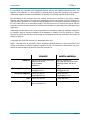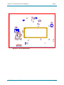
1
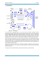
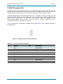
Cosmic Board for phyCORE-Vybrid
System on Module and Carrier Board
Hardware Manual
Document No: L-790e_1
Product No: PCL-052/POB-001
SOM PCB No: 1395.0
CB PCB No: 1393.1
Edition: August 30, 2013
A product of a PHYTEC Technology Holding Company
L-790e_1
Cosmic Board
In this manual are descriptions for copyrighted products that are not explicitly indicated as such. The
absence of the trademark (™) and copyright (©) symbols does not imply that a product is not protected.
Additionally, registered patents and trademarks are similarly not expressly indicated in this manual.
The information in this document has been carefully checked and is believed to be entirely reliable.
However, PHYTEC America LLC assumes no responsibility for any inaccuracies. PHYTEC America LLC
neither gives any guarantee nor accepts any liability whatsoever for consequential damages resulting from
the use of this manual or its associated product. PHYTEC America LLC reserves the right to alter the
information contained herein without prior notification and accepts no responsibility for any damages which
might result.
Additionally, PHYTEC America LLC offers no guarantee nor accepts any liability for damages arising from
the improper usage or improper installation of the hardware or software. PHYTEC America LLC further
reserves the right to alter the layout and/or design of the hardware without prior notification and accepts no
liability for doing so.
© Copyright 2011 PHYTEC America LLC, Bainbridge Island, WA.
Rights - including those of translation, reprint, broadcast, photomechanical or similar reproduction and
storage or processing in computer systems, in whole or in part - are reserved. No reproduction may occur
without the express written consent from PHYTEC America LLC.
EUROPE
NORTH AMERICA
PHYTEC Technologie Holding AG
Robert-Koch-Str. 39
D-55129 Mainz
GERMANY
PHYTEC America LLC
203 Parfitt Way SW, Suite G100
Bainbridge Island, WA 98110
USA
+49 (800) 0749832
[email protected]
1 (800) 278-9913
[email protected]
Technical Support:
+49 (6131) 9221-31
[email protected]
1 (800) 278-9913
[email protected]
Fax:
+49 (6131) 9221-33
1 (206) 780-9135
http://www.phytec.eu
http://www.phytec.de
http://www.phytec.com
Address:
Ordering Information:
Website:
© PHYTEC America LLC 2013
L-790e_1
Table of Contents
L-790e_1
Table of Contents
List of Tables. . . . . . . . . . . . . . . . . . . . . . . . . . . . . . . . . . . . . . . . . . . . . . . . . . . . . . . . . . ii
List of Figures . . . . . . . . . . . . . . . . . . . . . . . . . . . . . . . . . . . . . . . . . . . . . . . . . . . . . . . . .iii
Conventions, Abbreviations, and Acronyms . . . . . . . . . . . . . . . . . . . . . . . . . . . . . . . . . . . . . . . . . . . . iv
1 Introduction . . . . . . . . . . . . . . . . . . . . . . . . . . . . . . . . . . . . . . . . . . . . . . . . . . . . . . . . . . . . . . . . . . . . . . . 1
1.1 Cosmic Board Features . . . . . . . . . . . . . . . . . . . . . . . . . . . . . . . . . . . . . . . . . . . . . . . . . . . . . . 2
1.2 Block Diagram . . . . . . . . . . . . . . . . . . . . . . . . . . . . . . . . . . . . . . . . . . . . . . . . . . . . . . . . . . . . . 2
2 PCL-052/phyCORE-Vybrid System on Module . . . . . . . . . . . . . . . . . . . . . . . . . . . . . . . . . . . . . . . . . . . . 3
2.1 phyCORE-Vybrid Features . . . . . . . . . . . . . . . . . . . . . . . . . . . . . . . . . . . . . . . . . . . . . . . . . . . 3
3 Power . . . . . . . . . . . . . . . . . . . . . . . . . . . . . . . . . . . . . . . . . . . . . . . . . . . . . . . . . . . . . . . . . . . . . . . . . . . 5
3.1 Jumper Settings (JP1) . . . . . . . . . . . . . . . . . . . . . . . . . . . . . . . . . . . . . . . . . . . . . . . . . . . . . . . 5
3.2 USB Power (X6) . . . . . . . . . . . . . . . . . . . . . . . . . . . . . . . . . . . . . . . . . . . . . . . . . . . . . . . . . . . 5
3.3 Wall Power (X2). . . . . . . . . . . . . . . . . . . . . . . . . . . . . . . . . . . . . . . . . . . . . . . . . . . . . . . . . . . . 5
4 Ethernet (X3) . . . . . . . . . . . . . . . . . . . . . . . . . . . . . . . . . . . . . . . . . . . . . . . . . . . . . . . . . . . . . . . . . . . . . . 6
5 RS-232 Console (X10) . . . . . . . . . . . . . . . . . . . . . . . . . . . . . . . . . . . . . . . . . . . . . . . . . . . . . . . . . . . . . . 7
6 USB Connectivity. . . . . . . . . . . . . . . . . . . . . . . . . . . . . . . . . . . . . . . . . . . . . . . . . . . . . . . . . . . . . . . . . . . 8
6.1 USB Host (X3) . . . . . . . . . . . . . . . . . . . . . . . . . . . . . . . . . . . . . . . . . . . . . . . . . . . . . . . . . . . . . 8
6.2 USB OTG (X6). . . . . . . . . . . . . . . . . . . . . . . . . . . . . . . . . . . . . . . . . . . . . . . . . . . . . . . . . . . . . 8
7 SD Card (X18) . . . . . . . . . . . . . . . . . . . . . . . . . . . . . . . . . . . . . . . . . . . . . . . . . . . . . . . . . . . . . . . . . . . . . 9
7.1 Inserting and Removing an SD Card . . . . . . . . . . . . . . . . . . . . . . . . . . . . . . . . . . . . . . . . . . . . 9
8 HDMI (X16) . . . . . . . . . . . . . . . . . . . . . . . . . . . . . . . . . . . . . . . . . . . . . . . . . . . . . . . . . . . . . . . . . . . . . . 10
9 User Buttons . . . . . . . . . . . . . . . . . . . . . . . . . . . . . . . . . . . . . . . . . . . . . . . . . . . . . . . . . . . . . . . . . . . . . 11
10 System Reset Button (S5) . . . . . . . . . . . . . . . . . . . . . . . . . . . . . . . . . . . . . . . . . . . . . . . . . . . . . . . . . . 12
11 User LEDs . . . . . . . . . . . . . . . . . . . . . . . . . . . . . . . . . . . . . . . . . . . . . . . . . . . . . . . . . . . . . . . . . . . . . . 13
12 Boot Selection (JP2) . . . . . . . . . . . . . . . . . . . . . . . . . . . . . . . . . . . . . . . . . . . . . . . . . . . . . . . . . . . . . . 14
13 Expansion Connectors (X19, X20) . . . . . . . . . . . . . . . . . . . . . . . . . . . . . . . . . . . . . . . . . . . . . . . . . . . 15
14 OpenSDA Debug. . . . . . . . . . . . . . . . . . . . . . . . . . . . . . . . . . . . . . . . . . . . . . . . . . . . . . . . . . . . . . . . . 21
15 Technical Specifications . . . . . . . . . . . . . . . . . . . . . . . . . . . . . . . . . . . . . . . . . . . . . . . . . . . . . . . . . . . 22
16 Component Placement Diagrams . . . . . . . . . . . . . . . . . . . . . . . . . . . . . . . . . . . . . . . . . . . . . . . . . . . . 24
Revision History . . . . . . . . . . . . . . . . . . . . . . . . . . . . . . . . . . . . . . . . . . . . . . . . . . . . . . . . . . . . . . . . . . . 26
© PHYTEC America LLC 2013
i
List of Tables
L-790e_1
List of Tables
Table i-1. Abbreviations and Acronyms Used in This Manual . . . . . . . . . . . . . . . . . . . . . . . . . . . . iv
Table i-2. Types of Signals . . . . . . . . . . . . . . . . . . . . . . . . . . . . . . . . . . . . . . . . . . . . . . . . . . . . . . v
Table 3-1. Jumper Settings (JP1) . . . . . . . . . . . . . . . . . . . . . . . . . . . . . . . . . . . . . . . . . . . . . . . . . 5
Table 5-1. Connector X10 Pin Descriptions . . . . . . . . . . . . . . . . . . . . . . . . . . . . . . . . . . . . . . . . . 7
Table 12-1. Jumper Settings and Descriptions . . . . . . . . . . . . . . . . . . . . . . . . . . . . . . . . . . . . . . 14
Table 13-1. Power Signal Map . . . . . . . . . . . . . . . . . . . . . . . . . . . . . . . . . . . . . . . . . . . . . . . . . . 15
Table 13-2. System Signal Map . . . . . . . . . . . . . . . . . . . . . . . . . . . . . . . . . . . . . . . . . . . . . . . . . 15
Table 13-3. JTAG Signal Map . . . . . . . . . . . . . . . . . . . . . . . . . . . . . . . . . . . . . . . . . . . . . . . . . . . 15
Table 13-4. CAN Signal Map . . . . . . . . . . . . . . . . . . . . . . . . . . . . . . . . . . . . . . . . . . . . . . . . . . . . 16
Table 13-5. I2C Signal Map . . . . . . . . . . . . . . . . . . . . . . . . . . . . . . . . . . . . . . . . . . . . . . . . . . . . . 16
Table 13-6. UART Signal Map . . . . . . . . . . . . . . . . . . . . . . . . . . . . . . . . . . . . . . . . . . . . . . . . . . . 16
Table 13-8. ADC Signal Map . . . . . . . . . . . . . . . . . . . . . . . . . . . . . . . . . . . . . . . . . . . . . . . . . . . . 17
Table 13-9. DAC Signal Map . . . . . . . . . . . . . . . . . . . . . . . . . . . . . . . . . . . . . . . . . . . . . . . . . . . . 17
Table 13-7. QSPI Signal Map . . . . . . . . . . . . . . . . . . . . . . . . . . . . . . . . . . . . . . . . . . . . . . . . . . . 17
Table 13-10. SDHC Signal Map . . . . . . . . . . . . . . . . . . . . . . . . . . . . . . . . . . . . . . . . . . . . . . . . . 18
Table 13-11. LCD Signal Map . . . . . . . . . . . . . . . . . . . . . . . . . . . . . . . . . . . . . . . . . . . . . . . . . . . 18
Table 13-12. FlexBus Signal Map . . . . . . . . . . . . . . . . . . . . . . . . . . . . . . . . . . . . . . . . . . . . . . . . 19
Table 13-13. Miscellaneous Signal Map . . . . . . . . . . . . . . . . . . . . . . . . . . . . . . . . . . . . . . . . . . . 20
Table 15-1. Technical Specifications . . . . . . . . . . . . . . . . . . . . . . . . . . . . . . . . . . . . . . . . . . . . . . 23
Table 17-1. Revision History . . . . . . . . . . . . . . . . . . . . . . . . . . . . . . . . . . . . . . . . . . . . . . . . . . . . 26
© PHYTEC America LLC 2013
ii
List of Figures
L-790e_1
List of Figures
Fig. 1-1. Cosmic Board. . . . . . . . . . . . . . . . . . . . . . . . . . . . . . . . . . . . . . . . . . . . . . . . . . . . . . . . . . 1
Fig. 1-2. Cosmic Board Block Diagram . . . . . . . . . . . . . . . . . . . . . . . . . . . . . . . . . . . . . . . . . . . . . 2
Fig. 5-1. RS-232 Connector X10 Pin Numbering . . . . . . . . . . . . . . . . . . . . . . . . . . . . . . . . . . . . . . 7
Fig. 12-1. Jumper Numbering Scheme . . . . . . . . . . . . . . . . . . . . . . . . . . . . . . . . . . . . . . . . . . . . 14
Fig. 15-1. Cosmic Board Physical Dimensions. . . . . . . . . . . . . . . . . . . . . . . . . . . . . . . . . . . . . . . 22
Fig. 16-1. Cosmic Board Top . . . . . . . . . . . . . . . . . . . . . . . . . . . . . . . . . . . . . . . . . . . . . . . . . . . . 24
Fig. 16-2. Cosmic Board Bottom . . . . . . . . . . . . . . . . . . . . . . . . . . . . . . . . . . . . . . . . . . . . . . . . . 25
© PHYTEC America LLC 2013
iii
L-790e_1
Conventions, Abbreviations, and Acronyms
Conventions
The conventions used in this manual are as follows:
• Signals that are preceded by a “/” character are designated as active low signals. Their active
state is when they are driven low, or are driving low; for example: /RESET.
• Tables show the default setting or jumper position in bold, teal text.
• Text in blue indicates a hyperlink, either internal or external to the document. Click these links to
quickly jump to the applicable URL, part, chapter, table, or figure.
• References made to the phyCORE-Connector always refer to the high density Samtec connectors
on the underside of the Cosmic Board System on Module.
Abbreviations and Acronyms
Many acronyms and abbreviations are used throughout this manual. Use the table below to navigate
unfamiliar terms used in this document.
Table i-1. Abbreviations and Acronyms Used in This Manual
Abbreviation
Definition
BSP
Board Support Package (Software delivered with the Development Kit including an
operating system (Windows or Linux) preinstalled on the module and Development
Tools).
CB
Carrier Board; used in reference to the PCM-952/Cosmic Board Carrier Board
DFF
D flip-flop
EMB
External memory bus
EMI
Electromagnetic Interference
GPI
General purpose input
GPIO
General purpose input and output
GPO
General purpose output
IRAM
Internal RAM; the internal static RAM on the Freescale VFx00 processor
J
Solder jumper; these types of jumpers require solder equipment to remove and
place
JP
Solderless jumper; these types of jumpers can be removed and placed by hand with
no special tools
PCB
Printed circuit board
PDI
PHYTEC Display Interface; defined to connect PHYTEC display adapter boards or
custom adapters
PEB
PHYTEC Extension Board
PMIC
Power Management Integrated Circuit
PoE
Power over Ethernet
PoP
Package on Package
PoR
Power-on reset
RTC
Real-time clock
SMT
Surface mount technology
© PHYTEC America LLC 2013
iv
L-790e_1
Table i-1. Abbreviations and Acronyms Used in This Manual
Abbreviation
Definition
SOM
System on Module; used in reference to the PCM-052/Cosmic Board System on
Module
Sx
User button Sx (S1, S2, etc.) used in reference to the available user buttons, or DIP
switches on the Carrier Board
Sx_y
Switch y of DIP switch Sx; used in reference to the DIP switch on the Carrier Board
TRM
Technical Reference Manual
VBAT
SOM battery supply input
Different types of signals are brought out at the phyCORE-Connector. The following table lists the
abbreviations used to specify the type of a signal.
Table i-2. Types of Signals
Type of Signal
Description
Abbreviation
Power
Supply voltage
PWR
Ref-Voltage
Reference voltage
REF
USB-Power
USB voltage
USB
Input
Digital input
IN
Output
Digital output
OUT
Input with pull-up
Input with pull-up (jumper or open-collector output)
IPU
Input/output
Bidirectional input/output
IO
5V Input with pull-down
5V tolerant input with pull-down
5V_PD
LVDS
Differential line pairs 100 Ohm LVDS Pegel
LVDS
Differential 90 Ohm
Differential line pairs 90 Ohm
DIFF90
Differential 100 Ohm
Differential line pairs 100 Ohm
DIFF100
Analog
Analog input or output
Analog
© PHYTEC America LLC 2013
v
L-790e_1
Preface
This Cosmic Board Hardware Manual describes the System on Module's design and functions. Precise
specifications for the Freescale VFx00 processor can be found in the processor datasheet and/or user's
manual.
In this hardware manual and in the schematics, active low signals are denoted by a "/" preceding the signal
name, for example: /RD. A "0" represents a logic-zero or low-level signal, while a "1" represents a logicone or high-level signal.
Declaration of Electro Magnetic Conformity of the PHYTEC
Cosmic Board
PHYTEC System on Modules (SOMs) are designed for installation in electrical appliances or, combined
with the PHYTEC Carrier Board, can be used as dedicated Evaluation Boards (for use as a test and
prototype platform for hardware/software development) in laboratory environments.
CAUTION:
PHYTEC products lacking protective enclosures are subject to damage by ESD and, hence, may only be
unpacked, handled or operated in environments in which sufficient precautionary measures have been
taken in respect to ESD-dangers. It is also necessary that only appropriately trained personnel (such as
electricians, technicians and engineers) handle and/or operate these products. Moreover, PHYTEC
products should not be operated without protection circuitry if connections to the product's pin header
rows are longer than 3 m.
PHYTEC products fulfill the norms of the European Union's Directive for Electro Magnetic Conformity only
in accordance to the descriptions and rules of usage indicated in this hardware manual (particularly in
respect to the pin header row connectors, power connector and serial interface to a host-PC).
Implementation of PHYTEC products into target devices, as well as user modifications and extensions of
PHYTEC products, is subject to renewed establishment of conformity to, and certification of, Electro
Magnetic Directives. Users should ensure conformance following any modifications to the products as
well as implementation of the products into target systems.
The Cosmic Board is one of a series of PHYTEC System on Modules that can be populated with different
controllers and, hence, offers various functions and configurations. PHYTEC supports a variety of 8-/16and 32-bit controllers in two ways:
1. As the basis for Rapid Development Kits which serve as a reference and evaluation platform.
2. As insert-ready, fully functional phyCORE OEM modules, which can be embedded directly into the
user's peripheral hardware design.
Implementation of an OEM-able SOM subassembly as the "core" of your embedded design allows you to
focus on hardware peripherals and firmware without expending resources to "re-invent" microcontroller
circuitry. Furthermore, much of the value of the phyCORE module lies in its layout and test.
Production-ready Board Support Packages (BSPs) and Design Services for our hardware further reduce
development time and expenses. Take advantage of PHYTEC products to shorten time-to-market, reduce
development costs, and avoid substantial design issues and risks. For more information go to:
http://www.phytec.com/services/design-services/index.html
© PHYTEC America LLC 2013
vi
L-790e_1
Product Change Management
In addition to our HW and SW offerings, the buyer will receive a free obsolescence maintenance service
for the HW provided when purchasing a PHYTEC SOM.
Our Product Change Management Team of developers is continuously processing all incoming PCN's
(Product Change Notifications) from vendors and distributors concerning parts which are being used in our
products. Possible impacts to the functionality of our products, due to changes of functionality or obsolesce
of a certain part, are evaluated in order to take the right measures in purchasing or within our HW/SW
design.
Our general philosophy here is: We never discontinue a product as long as there is demand for it.
Therefore a set of methods has been established to fulfill our philosophy:
Avoidance strategies
• Avoid changes by evaluating longevity of a parts during design-in phase.
• Ensure availability of equivalent second source parts.
• Maintain close contact with part vendors for awareness of roadmap strategies.
Change management in case of functional changes
• Avoid impacts on Product functionality by choosing equivalent replacement parts.
• Avoid impacts on Product functionality by compensating changes through HW redesign or
backward compatibility
SW maintenance
• Provide early change notifications concerning functional relevant changes of our Products.
Change management in rare event of an obsolete and non replaceable part
• Ensure long term availability by stocking parts through last time buy management, according to
product forecasts.
• Offer long term frame contract to customers.
We refrain from providing detailed, part-specific information within this manual, which is subject to
changes, due to ongoing part maintenance for our products.
© PHYTEC America LLC 2013
vii
Chapter 1: Introduction
L-790e_1
1 Introduction
Fig. 1-1. Cosmic Board
The Cosmic Board for phyCORE-Vybrid is a low-cost, feature-rich software development platform
supporting the FreescaleTM Vybrid VF5xx and VF6xx processor families. At the core of the Cosmic board
is the PCL-052/phyCORE-Vybrid System On Module (SOM) in a direct solder form factor, containing the
processor, DRAM, NAND Flash, power regulation, supervision, transceivers, and other core functions
required to support the Vybrid processor. Surrounding the SOM is the POB-001/Cosmic Carrier Board,
adding power input, buttons, connectors, signal breakout, and HDMI connectivity amongst other things.
The PCL-052 System On Module is a connector-less, BGA style variant of the PCM-052/phyCORE-Vybrid
SOM. Unlike traditional PHYTEC SOM products that support high density connectors, the PCL-052 SOM
is directly soldered down to its Carrier Board using PHYTEC's Direct Solder Connect technology. This
solution offers an ultra-low cost Single Board Computer for the Vybrid processor, while maintaining most of
the advantages of the SOM concept.
Adding the phyCORE-Vybrid SOM into your own design is as simple as ordering the connectored version
(PCM-052) and making use of our Cosmic Carrier Board (POB-001), or RDK Carrier Board (PCM-952)
reference schematics.
A summary of the Cosmic Board features, along with a block diagram are presented below.
© PHYTEC America LLC 2013
1
Chapter 1: Introduction
L-790e_1
1.1 Cosmic Board Features
•
•
•
•
•
•
•
•
•
•
•
•
•
phyCORE-Vybrid System On Module
Board power over:
- USB OTG Connector
- Wall Adapter Input
High Speed USB Host Connector (standard A)
High Speed USB OTG Connector (micro AB)
10/100 Ethernet RJ-45 Jack
Micro SD Card Slot
Micro HDMI connector supporting 640x480 @ 24bpp
RS-232 Console Connectivity via DB-9
Boot Selection Jumpers (NAND or SD Card)
Hardware Debug via OpenSDA over USB (Cosmic+ kit only)
4x User Buttons
4x User LEDs
120-pin, 2mm header socket for easy access to Vybrid processor signals
1.2 Block Diagram
Fig. 1-2. Cosmic Board Block Diagram
© PHYTEC America LLC 2013
2
Chapter 2: PCL-052/phyCORE-Vybrid System on Module
L-790e_1
2 PCL-052/phyCORE-Vybrid System on Module
This chapter gives a brief introduction to the PCL-052/phyCORE-Vybrid System on Module (SOM),
highlighting its benefits and features. For more detailed information, please refer to the Hardware Manual
for the modular, connectored version of the SOM (PCM-052) by clicking here.
The phyCORE-Vybrid belongs to PHYTEC’s phyCORE System on Module (SOM) family. The
phyCORE SOMs represent the continuous development of PHYTEC SOM technology. Like its mini-,
micro-, and nanoMODUL predecessors, the phyCORE boards integrate all core elements of a
microcontroller system on a subminiature board and are designed in a manner that ensures their easy
expansion and embedding in peripheral hardware developments.
As independent research indicates that approximately 70% of all EMI (Electro Magnetic Interference)
problems stem from insufficient supply voltage grounding of electronic components in high frequency
environments, the phyCORE board design features an increased pin package. The increased pin package
allows dedication of approximately 20% of all connector pins on the phyCORE boards to ground. This
improves EMI and EMC characteristics and makes it easier to design complex applications meeting EMI
and EMC guidelines using phyCORE boards even in high noise environments.
phyCORE boards achieve their small size through modern SMD technology and multi-layer design. In
accordance with the complexity of the module, 0402-packaged SMD components and laser-drilled
Microvias are used on the boards, providing phyCORE users with access to this cutting edge
miniaturization technology for integration into their own design.
The PCM-052, connectored version of the phyCORE-Vybrid is a sub-miniature (41 x 51 mm) insert-ready
SOM populated with Freescale FVx00 processor. Its universal design enables its insertion into a wide
range of embedded applications. All processor signals and ports extend from the processor to high-density
pitch (0.5 mm) connectors aligning two sides of the board. This allows the SOM to be plugged like a "big
chip" into a target application.
The PCL-052, connectorless version of the phyCORE-Vybrid populating the Cosmic Board is identical to
the connectored version, with the exception of the connection interface. Instead of two high density
connectors aligning the edges of the board, the PCL-052 solders directly down to its Carrier Board with a
BGA style footprint.
Precise specifications for the processor populating the board can be found in the applicable processor
user's manual and datasheet. The descriptions in this manual are based on the Freescale FVx00
processor. No description of compatible processor derivative functions is included, as such functions are
not relevant for the basic functioning of the Cosmic Board.
2.1 phyCORE-Vybrid Features
•
•
•
•
•
•
•
Insert-ready, sub-miniature (41 mm x 51 mm) System on Module (SOM) subassembly in low EMI
design, achieved through advanced SMD technology
Populated with the Freescale FVx00 Single (Cortex-A5) or heterogenous Dual Core (Cortex-A5
and Cortex-M4) processor
Max. 500 MHz core clock frequency for the Cortex-A5, 167 MHz for the Cortex-M4
Boot from NAND Flash or SPI Flash
Controller signals and ports extend to two BGA-style connection interfaces aligning two sides of
the board, enabling it to be soldered directly into the target application
Single supply voltage of 3.3 V (max.1 A)
All controller required supplies generated on board
© PHYTEC America LLC 2013
3
Chapter 2: PCL-052/phyCORE-Vybrid System on Module
•
•
•
•
•
•
•
•
•
•
•
•
•
•
•
•
•
•
•
•
•
•
•
L-790e_1
Improved interference safety achieved through multi-layer PCB technology and dedicated ground
pins
256 MB (up to 2 GB) on-board NAND Flash1
128/256/512 MB DDR3 SDRAM 1
4 kB (up to 32 kB) I2C EEPROM1
32 MB (up to 128 MB) SPI Flash
Two RS-232 two-signal (Tx/Rx) serial interfaces, or one RS-232 interface with hardware flow
control, configured through software
Six UARTs
Dual USB OTG 2.0 High-Speed Controller with PHY
Two 10/100 MBit Ethernet interfaces with internal L2-Switch and IEEE1588 PTP for Realtime
Ethernet (available as RMII TTL signals or 10/100 differential pairs)
Four I2C interfaces with SMBUS support
Four Serial Peripheral Interfaces (SPI)
Two Quad SPI (QSPI) supporting XIP
Two FlexCAN interfaces with transceivers
Display interface with 24 data bits
I2S audio
Two 12-bit digital to analog converter (DAC) outputs
Two 10-channel, 12-bit analog to digital (ADC) inputs
JTAG
16-bit Trace port
Two active and two passive tamper security signals
4-bit Secure Digital Host interface (SD/MMC)
Real-Time Clock
-40 to 85 C operating temperature range
1. The maximum memory size listed is as of the printing of this manual. Please contact PHYTEC for more information
about additional, or new module configurations available.
© PHYTEC America LLC 2013
4
Chapter 3: Power
L-790e_1
3 Power
Power is supplied to the system using two methods:
1. USB power via connector X6
2. Wall power via connector X2
USB power provides an easy, single-cable solution for both power and console connectivity. System
functionality is limited when powering the board off of USB. Most features of the board will function under
USB power, with the exception of USB host and any add-on boards connected via the Expansion
Connectors. Select the power option by configuring jumper JP1 using Table 3-1 below.
3.1 Jumper Settings (JP1)
Table 3-1. Jumper Settings (JP1)
Jumper
Position
Description
1+2
Wall Power
2+3
USB Power
See Figure 1-1 for the location of jumper JP1. Pin 1 is marked on the PCB with a clipped corner on the
component outline silk screen.
3.2 USB Power (X6)
USB power can be used if the USB host interface is not required, nor any add-on boards connected to the
Expansion Connectors (X19, X20) are required.
Use a standard USB-A to micro-AB, or micro-B connected to a PC to power the board and provide console
access. A wall-outlet charger can be used to power the board but will eliminate the use of serial over USB.
Configure the board for USB power by setting JP1 to 2+3. See Figure 1-1 for the location of jumper JP1.
3.3 Wall Power (X2)
Wall power should be used when USB host, or expansion connector add-on boards are used. Both
scenarios draw additional power not available through the USB OTG connector at X6.
A suitable +5VDC +- 5% / 1A or greater wall power adapter should be used with a center positive contact.
An appropriate power supply can be ordered with the kit at the time you place your order.
Configure the board for wall power by setting JP1 to 1+2. See Figure 1-1 for the location of jumper JP1.
CAUTION:
Do not use a laboratory adapter to supply power to the Carrier Board! Power spikes during power-on
could destroy the phyCORE module mounted on the Carrier Board. Do not change jumper settings while
the Carrier Board is supplied with power.
© PHYTEC America LLC 2013
5
Chapter 4: Ethernet (X3)
L-790e_1
4 Ethernet (X3)
The 10/100 ETH1 interface, derived from the Vybrid processor RMII1 signals, is accessible at an RJ-45
connector at X3 (USB Dual Standard A and Ethernet).
LEDs are integrated on the connector for indication of LINK (green) and SPEED (yellow).
The Ethernet PHY on the SOM supports the HP Auto-MDIX function, eliminating the need for
considerations of a direct connect LAN cable or cross-over patch cable. The transceivers detect the TX
and RX signals of the connected devices and automatically configure their RX and TX pins accordingly.
© PHYTEC America LLC 2013
6
Chapter 5: RS-232 Console (X10)
L-790e_1
5 RS-232 Console (X10)
The DB9 connector X10 provides connectivity to the Vybrid SCI1 (UART) signals at RS-232 level. This
interface does not include the Vybrid's SCI1_RTS and SCI1_CTS signals for flow control. This connection
is provided primarily for console access, but could be reconfigured for other purposes if needed.
A standard straight-through serial cable connected to a PC is required to access this console port. This
port has the benefit of providing access to U-Boot and to early Linux boot log message, as opposed to the
console access provided over the USB port, which provides neither. Use appropriate serial
communications software such as minicom for Linux, or putty for Windows. Configure the port for
115200,8,N,1 (8 data bits, no handshake, 1 stop bit).
Figure 5-1 shows the pin numbering for the DB9 connector, while Table 5-1 gives a detailed description of
the signals at X10.
Fig. 5-1. RS-232 Connector X10 Pin Numbering
Table 5-1. Connector X10 Pin Descriptions
Pin
Signal
I/O
Description
1
N/C
-
Not connected
2
SCI1_TX_RS232
O
SCI1 transmit
3
SCI1_RX_RS232
I
SCI1 receive
4
N/C
-
Not connected
5
GND
-
GND
6
N/C
-
Not connected
7
N/C
-
Not connected
8
N/C
-
Not connected
9
N/C
-
Not connected
© PHYTEC America LLC 2013
7
Chapter 6: USB Connectivity
L-790e_1
6 USB Connectivity
6.1 USB Host (X3)
The USB1 interface signals route to the bottom connector of X3 (USB Dual Standard A and Ethernet). Note
that the top USB connector of X3 is a not used. Although the USB interface of the Vybrid processor
complies with USB 2.0 HS specification and supports dual role device configuration, due to its USB-A style
connector, USB1 is limited to Host operation only.
The USB1 interface on the Cosmic board is equipped with ESD protection. It has its own 5V supply that is
current limited by U4 (TPS2051B). It supports connection of different USB devices such as mass storage
device, keyboard, and mouse.
To use the USB Host interface the board must be configured to provide power from the wall adapter input
at X2 (see Figure 1-1). Set jumper JP1 to 1+2 to configure the board for wall power.
6.2 USB OTG (X6)
The USB0 interface signals route to connector X6 (USB Micro-AB). The USB interface of the Vybrid
processor complies with USB 2.0 HS specification. Firmware interaction configures the interface to act in
Host or Device mode, making it a dual role device but not a true OTG controller as described in more detail
in the Vybrid processor Reference Manual.
The USB0 interface on the Cosmic board is equipped with ESD protection. VBUS_USB0 is connected to
VBUS of the cable meaning USB0 is powered by the host.
This interface can be used both to power the board, and to provide serial console access. Connect a USB
Standard-A to Micro-B, or Micro-AB cable between a host PC and connector X6. To configure the board for
USB power, set jumper JP1 to 2+3 (see Figure 1-1). Once booted, the Cosmic Board shows up as a virtual
serial port over USB. Use appropriate serial communications software such as minicom for Linux, or putty
for Windows. Configure the port for 115200,8,N,1 (8 data bits, no handshake, 1 stop bit).
© PHYTEC America LLC 2013
8
Chapter 7: SD Card (X18)
L-790e_1
7 SD Card (X18)
The Cosmic board provides a Micro SD card slot at X18 for connection to the Vybrid's SDHC1 interface.
The interface is powered by an instant-on 3.3 V power supply and has card detect support (CDET) via the
Vybrid processor PTB28 signal.
In addition to mass storage usage, the processor can boot from this interface. As the default boot mode of
the phyCORE-Vybrid SOM, SD boot is selected by opening JP2 (see Figure 1-1).
7.1 Inserting and Removing an SD Card
Insert a micro SD Card into slot X18, label down and pins facing up. After aligning the card with the
connector, push to insert. The card will make a clicking sound and latch into the connector. To eject the
card, push the card in to release. The connector will click and the card will be safe to remove. To avoid
damaging the connector do not attempt to pull the card directly out without first pushing inward to release
the lock mechanism.
© PHYTEC America LLC 2013
9
Chapter 8: HDMI (X16)
L-790e_1
8 HDMI (X16)
A High-Definition Multimedia Interface (HDMI) transmitter is connected to the parallel display interface of
the processor. The interface is compliant with HDMI 1.4a specification and available through the micro
HDMI connector at X16. Connection to an HDMI display is limited to 640x480 @ 24bpp due to Vybrid
processor limitations and compatible display clock frequency limitations.
The 24-bit Vybrid LCD interface (3 x 8-bit RGB) along with the I2S-bus are converted to HDMI signals by
the HDMI transmitter at U1. The transmitter is configured by the processor via I2C and although operating
at 1.8V, can handle the 3.3V processor signals. Along with delivering Consumer Electronic Control (CEC)
the device also supports a low power or standby mode when HDMI is not being used. A port protection and
interface device at U13 provides ESD protection, integrated level shifting of HDMI signals, and a 50 mA /
5V current-limited supply to the HDMI sink device (monitor, TV, projector, etc).
For access to the HDMI output, a micro HDMI cable is required. For connection to general HDMI compliant
devices, an HDMI to Micro HDMI cable will typical be used.
The display signals that are connected to the HDMI interface (PTE0 to PTE28) are available at the
expansion connector so that they can be used for other purposes such as connecting to an LCD expansion
board. Refer to Chapter 13 for additional information.
© PHYTEC America LLC 2013
10
Chapter 9: User Buttons
L-790e_1
9 User Buttons
The Cosmic board is populated with four user accessible push buttons located at S1, S2, S3, and S4 to
enable user input (see Figure 1-1). Each button is connected to a GPIO on the Vybrid processor. A detailed
list of the user buttons is presented below.
S1
User Button 1 (BTN1). Pressing this button generates a debounced, active high signal to the
processor at MCU_PTB3. Holding this button will keep the output to MCU_PTB3 held high.
Releasing this button will keep the output to MCU_PTB3 held low.
S2
User Button 2 (BTN2). Pressing this button generates a debounced, active high signal to the
processor at MCU_PTB8. Holding this button will keep the output to MCU_PTB8 held high.
Releasing this button will keep the output to MCU_PTB8 held low.
S3
User Button 3 (BTN3). Pressing this button generates a debounced, active high signal to the
processor at MCU_PTB9. Holding this button will keep the output to MCU_PTB9 held high.
Releasing this button will keep the output to MCU_PTB9 held low.
S4
User Button 4 (BTN4). Pressing this button generates a debounced, active high signal to the
processor at MCU_PTB12. Holding this button will keep the output to MCU_PTB12 held
high. Releasing this button will keep the output to MCU_PTB12 held low.
© PHYTEC America LLC 2013
11
Chapter 10: System Reset Button (S5)
L-790e_1
10 System Reset Button (S5)
The Cosmic Board is equipped with a system reset button at S5. Pressing the button will toggle the
nRESET_IN signal low and generate a manual system reset driving RESETn on the phyCORE-Vybrid low.
The system reset signal, RESETn, is available on the Expansion connector (see Chapter 13 for more
information) and can be used to reset various other peripheral devices. Refer to the PCM-052/phyCOREVybrid Hardware Manual for details on the RESETn signal.
CAUTION:
When running Linux a proper system shutdown should be performed, or reboot executed instead of
pressing the reset button. Pressing the reset button (or cutting power) without properly shutting down can
cause file system errors and is not advised. Issue a poweroff or reboot command at the Linux prompt to
avoid file system damage. Only use the reset button when not running Linux, or if the system freezes up.
© PHYTEC America LLC 2013
12
Chapter 11: User LEDs
L-790e_1
11 User LEDs
The Cosmic board is populated with four user programmable LEDs located at D11, D10, D4, and D5 to
provide visual feedback to the user (see Figure 1-1). Each LED is connected to a GPIO on the Vybrid
processor. A detailed list of the user LEDs is presented below.
D11
LED1 (Green). Connected to processor signal MCU_PTB13. Drive signal MCU_PTB13 high
to turn this LED on and low to turn this LED off.
D10
LED2 (Green). Connected to processor signal MCU_PTB18. Drive signal MCU_PTB18 high
to turn this LED on and low to turn this LED off.
D4
LED3 (Red). Connected to processor signal MCU_PTB26. Drive signal MCU_PTB26 high to
turn this LED on and low to turn this LED off.
D5
LED4 (Red). Connected to processor signal MCU_PTB29. Drive signal MCU_PTB29 high to
turn this LED on and low to turn this LED off.
© PHYTEC America LLC 2013
13
Chapter 12: Boot Selection (JP2)
L-790e_1
12 Boot Selection (JP2)
Jumper JP2 provides a way to override the default boot option configured on the Vybrid SOM.
Fig. 12-1. Jumper Numbering Scheme
Figure 12-1 shows the jumper pin numbering scheme. Pin 1 on the board is marked with a number one on
the PCB silk screen. It is also visibly marked with a clipped corner on the component outline.
Table 12-1 shows the required jumper positions for configuring the desired boot device. Use jumper wires
to connect the pins of JP2 based on the settings described.
By default JP2 is open, configuring the Vybrid for SD card boot.
Table 12-1. Jumper Settings and Descriptions
Jumper
Setting
Boot Device
JP2
OPEN
SD Card
1+2
3+4
5+6
NAND
© PHYTEC America LLC 2013
14
Chapter 13: Expansion Connectors (X19, X20)
L-790e_1
13 Expansion Connectors (X19, X20)
Two 2x30 2mm Expansion connectors (X19 and X20) provide easy access to many of the phyCOREVybrid signals. All processor signals on the Expansion connector are 3.3 V. As an accessory, add-on
expansion boards such as LCD and WiFi are made available through PHYTEC to connect to the
Expansion connectors.
Most of the signals routed to the expansion connector have been configured for a given pin muxed
function. Using these signals are alternate functions requires BSP modifications.
Tables detailing signal mapping of the Expansion Connectors are provided below. These tables list only the
primary function intended on the Cosmic Board, but can be reconfigured for many other purposes. Refer to
the Vybrid Technical Reference manual on available operation modes.
Table 13-1. Power Signal Map
Signal
Expansion Connector Pin
Description
VCC_5V0
X19-1, X19-3
5V power from currently selected source
(wall or USB)
VCC_3V3
X19-2, X19-4
3.3V voltage domain
5V_IN
X19-5
5V power from wall adapter input
VCC_1V8
X19-6
1.8V voltage domain
VBUS_USB0
X19-8
5V power from USB OTG connector
GND
X19-7, X19-10, X19-59, X19-60,
X20-1, X20-2, X20-59, X20-60
Ground
Table 13-2. System Signal Map
Signal
Expansion
Board Pin
Type
Description
RESETn
X20-58
O
System reset signal; can be used to reset external
devices. This is an open-drain output with a 4.7K
pull-up on the SOM.
MCU_PTB11
X19-11
O
CKO2; free for external use
MCU_PTA12
X19-21
O
TRACECK; free for external use
Table 13-3. JTAG Signal Map
Signal
Expansion
Board Pin
Type
Description
MCU_PTA8
X19-14
I
JTCLK; connected to POB-001 K20 SW_CLK for
Serial Wire Debug
© PHYTEC America LLC 2013
15
Chapter 13: Expansion Connectors (X19, X20)
L-790e_1
Table 13-3. JTAG Signal Map
Signal
Expansion
Board Pin
Type
Description
MCU_PTA9
X19-16
I
JTDI; free for external use
MCU_PTA10
X19-18
O
JTDO; free for external use
MCU_PTA11
X19-20
I
JTMS; connected to POB-001 K20 SW_DO and
SW_DI for Serial Wire Debug
Table 13-4. CAN Signal Map
Signal
Expansion
Board Pin
Type
Description
MCU_PTB14
X19-22
I
CAN0_RX; connected to PCL-052 CAN transceiver
MCU_PTB15
X19-24
O
CAN0_TX; connected to PCL-052 CAN transceiver
MCU_PTB16
X19-31
I
CAN1_RX; connected to PCL-052 CAN transceiver
MCU_PTB17
X19-33
O
CAN1_TX; connected to PCL-052 CAN transceiver
Table 13-5. I2C Signal Map
Signal
Expansion
Board Pin
Type
Description
MCU_PTB14
X19-22
I/O
I2C0_SCL; connected to PCL-052 CAN transceiver
MCU_PTB15
X19-24
I/O
I2C0_SDA; connected to PCL-052 CAN transceiver
MCU_PTA22
X19-27
I/O
I2C2_SCL; connected to PCL-052 RTC and
EEPROM with external 2.2k pull-up and POB-001
HDMI transceiver
MCU_PTA23
X19-29
I/O
I2C2_SDA; connected to PCL-052 RTC and
EEPROM with external 2.2k pull-up and POB-001
HDMI transceiver
MCU_PTA30
X19-35
I/O
I2C3_SCL; free for external use
MCU_PTA31
X19-37
I/O
I2C3_SDA; free for external use
Table 13-6. UART Signal Map
Signal
Expansion
Board Pin
Type
Description
MCU_PTA20
X19-23
O
SCI3_TX serial transmit signal; free for external use
MCU_PTA21
X19-25
I
SCI3_RX serial receive signal; free for external use
© PHYTEC America LLC 2013
16
Chapter 13: Expansion Connectors (X19, X20)
L-790e_1
Table 13-7. QSPI Signal Map
Signal
Expansion
Board Pin
Type
Description
MCU_PTD0
X19-46
O
QSPIA_SCK; free for external use
MCU_PTD1
X19-48
O
QSPIA_CS0; free for external use
MCU_PTD2
X19-50
I/O
QSPIA_IO3; free for external use
MCU_PTD3
X19-52
I/O
QSPIA_IO2; free for external use
MCU_PTD4
X19-54
I/O
QSPIA_IO1; free for external use
MCU_PTD5
X19-56
I/O
QSPIA_IO0; free for external use
MCU_PTD6
X19-58
O
QSPIA_DQS; free for external use
MCU_PTD7
X19-26
O
QSPIB_SCK; free for external use
MCU_PTD8
X19-28
O
QSPIB_CD0; free for external use
MCU_PTD9
X19-30
I/O
QSPIB_IO3; free for external use
MCU_PTD10
X19-32
I/O
QSPIB_IO2; free for external use
MCU_PTD11
X19-34
I/O
QSPIB_IO1; free for external use
MCU_PTD12
X19-36
I/O
QSPIB_IO0; free for external use
MCU_PTD13
X19-38
O
QSPIB_DQS; free for external use
Table 13-8. ADC Signal Map
Signal
Expansion
Board Pin
Type
Description
ADC0SE8
X19-42
Analog
ADC input; free for external use
ADC0SE9
X19-41
Analog
ADC input; free for external use
ADC1SE8
X19-39
Analog
ADC input; free for external use
ADC1SE9
X19-40
Analog
ADC input; free for external use
Table 13-9. DAC Signal Map
Signal
Expansion
Board Pin
Type
Description
DACO0
X19-44
Analog
DAC output; free for external use
DACO1
X19-43
Analog
DAC output; free for external use
© PHYTEC America LLC 2013
17
Chapter 13: Expansion Connectors (X19, X20)
L-790e_1
Table 13-10. SDHC Signal Map
Signal
Expansion
Board Pin
Type
Description
MCU_PTC0
X19-45
O
SDHC0_CLK; free for external use
MCU_PTC1
X19-47
I/O
SDHC0_CMD; free for external use
MCU_PTC2
X19-49
I/O
SDHC0_DAT0; free for external use
MCU_PTC3
X19-51
I/O
SDHC0_DAT1; free for external use
MCU_PTC4
X19-53
I/O
SDHC0_DAT2; free for external use
MCU_PTC5
X19-55
I/O
SDHC0_DAT3; free for external use
MCU_PTC6
X19-57
I
SDHC0_WP; free for external use
Table 13-11. LCD Signal Map
Signal
Expansion
Board Pin
Type
Description
MCU_PTE0
X20-3
I/O
LCD0; connected to BOOTMOD1 with external 10k pull-up
on reset and POB-001 HDMI transmitter
MCU_PTE1
X20-5
I/O
LCD1; connected to BOOTMOD1 with external 10k pulldown on reset and POB-001 HDMI transmitter
MCU_PTE2
X20-7
I/O
LCD2; connected to POB-001 HDMI transmitter
MCU_PTE3
X20-9
I/O
LCD3; available for external use
MCU_PTE4
X20-11
I/O
LCD4; connected to POB-001 HDMI transmitter
MCU_PTE5
X20-13
I/O
LCD5; connected to POB-001 HDMI transmitter
MCU_PTE6
X20-15
I/O
LCD6; connected to POB-001 HDMI transmitter
MCU_PTE7
X20-17
I/O
LCD7; connected to POB-001 HDMI transmitter. This pin is
connected to RCON0 which will be driven low on reset.
MCU_PTE8
X20-19
I/O
LCD8; connected to POB-001 HDMI transmitter. This pin is
connected to RCON1 which will be driven low on reset.
MCU_PTE9
X20-21
I/O
LCD9; connected to POB-001 HDMI transmitter. This pin is
connected to RCON2 which will be driven high on reset.
MCU_PTE10
X20-23
I/O
LCD10; connected to POB-001 HDMI transmitter. This pin is
connected to RCON3 which will be driven low on reset.
MCU_PTE11
X20-25
I/O
LCD11; connected to POB-001 HDMI transmitter. This pin is
connected to RCON4 which will be driven low on reset.
MCU_PTE12
X20-27
I/O
LCD12; connected to POB-001 HDMI transmitter. This pin is
connected to RCON5 which will be driven based on the boot
settings (JP2).
MCU_PTE13
X20-29
I/O
LCD13; connected to POB-001 HDMI transmitter.
MCU_PTE14
X20-31
I/O
LCD14; connected to POB-001 HDMI transmitter
MCU_PTE15
X20-4
I/O
LCD15; connected to POB-001 HDMI transmitter. This pin is
connected to RCON6 which will be driven based on the boot
settings (JP2).
© PHYTEC America LLC 2013
18
Chapter 13: Expansion Connectors (X19, X20)
L-790e_1
Table 13-11. LCD Signal Map
Signal
Expansion
Board Pin
Type
Description
MCU_PTE16
X20-6
I/O
LCD16; connected to POB-001 HDMI transmitter. This pin is
connected to RCON7 which will be driven based on the boot
settings (JP2).
MCU_PTE17
X20-8
I/O
LCD17; connected to POB-001 HDMI transmitter. This pin is
connected to RCON8 which will be driven low on reset.
MCU_PTE18
X20-10
I/O
LCD18; connected to POB-001 HDMI transmitter. This pin is
connected to RCON9 which will be driven high on reset.
MCU_PTE19
X20-12
I/O
LCD19; connected to POB-001 HDMI transmitter. This pin is
connected to RCON10 which will be driven low on reset.
MCU_PTE20
X20-14
I/O
LCD20; connected to POB-001 HDMI transmitter. This pin is
connected to RCON11 which will be driven high on reset.
MCU_PTE21
X20-16
I/O
LCD21; connected to POB-001 HDMI transmitter
MCU_PTE22
X20-18
I/O
LCD22; connected to POB-001 HDMI transmitter
MCU_PTE23
X20-20
I/O
LCD23; connected to POB-001 HDMI transmitter. This pin is
connected to RCON12 which will be driven high on reset.
MCU_PTE24
X20-22
I/O
LCD24; connected to POB-001 HDMI transmitter This pin is
connected to RCON13 which will be driven high on reset.
MCU_PTE25
X20-24
I/O
LCD25; connected to POB-001 HDMI transmitter. This pin is
connected to RCON14 which will be driven high on reset.
MCU_PTE26
X20-26
I/O
LCD26; connected to POB-001 HDMI transmitter. This pin is
connected to RCON15 which will be driven high on reset.
MCU_PTE27
X20-28
I/O
LCD27; connected to POB-001 HDMI transmitter
MCU_PTE28
X20-30
I/O
LCD28; connected to POB-001 HDMI transmitter
Table 13-12. FlexBus Signal Map
Signal
Expansion
Board Pin
Type
Description
MCU_PTD16
X20-33
I/O
FB_AD16; connected to PCL-052 NAND Flash (U17)
MCU_PTD17
X20-35
I/O
FB_AD17; connected to PCL-052 NAND Flash (U17)
MCU_PTD18
X20-37
I/O
FB_AD18; connected to PCL-052 NAND Flash (U17)
MCU_PTD19
X20-39
I/O
FB_AD19; connected to PCL-052 NAND Flash (U17)
MCU_PTD20
X20-41
I/O
FB_AD20; connected to PCL-052 NAND Flash (U17)
MCU_PTD21
X20-43
I/O
FB_AD21; connected to PCL-052 NAND Flash (U17)
MCU_PTD22
X20-45
I/O
FB_AD22; connected to PCL-052 NAND Flash (U17)
MCU_PTD23
X20-32
I/O
FB_AD23; connected to PCL-052 NAND Flash (U17)
MCU_PTD24
X20-34
I/O
FB_AD24; connected to PCL-052 NAND Flash (U17)
MCU_PTD25
X20-36
I/O
FB_AD25; connected to PCL-052 NAND Flash (U17)
MCU_PTD26
X20-38
I/O
FB_AD26; connected to PCL-052 NAND Flash (U17)
MCU_PTD27
X20-40
I/O
FB_AD27; connected to PCL-052 NAND Flash (U17)
© PHYTEC America LLC 2013
19
Chapter 13: Expansion Connectors (X19, X20)
L-790e_1
Table 13-12. FlexBus Signal Map
Signal
Expansion
Board Pin
Type
Description
MCU_PTD28
X20-42
I/O
FB_AD28; connected to PCL-052 NAND Flash (U17)
MCU_PTD29
X20-44
I/O
FB_AD29; connected to PCL-052 NAND Flash (U17)
MCU_PTD30
X20-46
I/O
FB_AD30; connected to PCL-052 NAND Flash (U17)
MCU_PTD31
X20-48
I/O
FB_AD31; connected to PCL-052 NAND Flash (U17)
MCU_PTC26
X19-19
I/O
FB_TA_b; connected to PCL-052 NAND Flash (U17)
MCU_PTC27
X19-15
I/O
connected to PCL-052 NAND Flash (U17)
MCU_PTC28
X19-9
I/O
connected to PCL-052 NAND Flash (U17)
MCU_PTB24
X19-11
I/O
FB_CS4_b; connected to PCL-052 NAND Flash (U17)
MCU_PTB25
X19-17
I/O
FB_CS1_b; connected to PCL-052 NAND Flash (U17)
MCU_PTB27
X19-13
-
connected to PCL-051 NAND Flash (U17)
Table 13-13. Miscellaneous Signal Map
Signal
Expansion
Board Pin
Type
Description
MCU_PTB19
X20-47
I/O
This pin is connected will be driven low on reset.
MCU_PTB20
X20-49
I/O
free for external use
MCU_PTB21
X20-51
I/O
free for external use
MCU_PTB22
X20-53
I/O
free for external use
MCU_PTB23
X20-55
I/O
free for external use
MCU_PTC30
X20-57
I/O
free for external use
MCU_PTB0
X20-50
I/O
free for external use
MCU_PTB1
X20-52
I/O
free for external use
MCU_PTB2
X20-54
I/O
free for external use
MCU_PTC31
X20-56
I/O
free for external use
© PHYTEC America LLC 2013
20
Chapter 14: OpenSDA Debug
L-790e_1
14 OpenSDA Debug
USB Micro-B connector X5 provides OpenSDA and CMSIS-DAP access to the Vybrid processor for
debugging purposes on the Cosmic board. OpenSDA and CMSIS-DAP debugging are implemented
through a Freescale K20 processor (U3) on the Carrier Board.
The K20 circuit communicates to the host PC via USB and then to the processor via the Vybrid Debug
Access Port (DAP) signals MCU_PTA8 and MCU_PTA11. The system can be reset directly with the K20's
GPIO signal PTB1. Use the debugger's system reset function to reset the Vybrid processor.
A USB Standard-A to Micro-B cable connected between the Host-PC and X5 allows the processor to be
interactively controlled with debugging software such as ARM Development Suite (DS-5™). Refer to the
Quickstart for the Cosmic Board for more information.
NOTE:
OpenSDA debug circuit is only populated on the Cosmic+ kit version.
© PHYTEC America LLC 2013
21
Chapter 15: Technical Specifications
L-790e_1
15 Technical Specifications
The physical dimensions of the Cosmic Board for phyCORE-Vybrid are presented in Figure 15-1. A
summary of technical specifications is provided in Table 15-1.
Fig. 15-1. Cosmic Board Physical Dimensions
© PHYTEC America LLC 2013
22
Chapter 15: Technical Specifications
L-790e_1
Table 15-1. Technical Specifications1
Dimensions 100 x 72mm
Weight 64.2g / 2.26oz typ.
Storage Temperature -40 °C to +125 °C
Operating Temperature 0 °C to +70 °C (commercial)
Humidity 95% r.F. not condensed
Operating Voltage +5VDC +- 5%
Power Consumption 1.83W typ.; Linux booted from uSD card, running ping test
1. These specifications describe the standard configuration of the Cosmic Board as of the printing of this manual.
© PHYTEC America LLC 2013
23
Chapter 16: Component Placement Diagrams
L-790e_1
16 Component Placement Diagrams
PCBX6
Edge
1
C46
R55
X14
C26 R52
R29
R78
R79
U13
R80
X3
R63
R77
R81
U4
U12
C42
R48
C8 R15
X17
underside space 12,5mm
X4
underside space 6,3mm
U7
R69
L5
Clearance pad to trace >508µm
R68 R67 C41 R72
R26 R27
R82 C54 R84
S5
C40
X15
D8
C21
C24
C50
TP7
C10
R75
R76
R41
S4
JP2
TP4
C17
S3
NoU1
Vias
R65
S2
R64R66
R7
R3
C30
R8
R4
C32
R9
R5
C33
R10
R6
C34
S1
C23
C20
X8
C53
R83
X16
L4
C3
X20
X19
C7
C9
D9
C12
D7
JP1
C1 C6
C25
X18
C39
PCBX5
Edge
D12
C45
R53
C35
D6
U6
R2
X13
D5 R30
D4 R33
D10 R31
D11 R32
C16
X2
C14
X1
X12
Fig. 16-1. Cosmic Board Top
© PHYTEC America LLC 2013
24
Chapter 16: Component Placement Diagrams
L-790e_1
C18
L3
C43
D3
TP6
C37
L1
R73 U2
C27
R44
R43
R42
C28
C38
C22
D2
C19
C29
R28
R85
R86 R50
U5
C11
R49
R45 C31
C48
C4 C49
R57
R58
C5
R1
R12 R13
R60
R61
C13
C2
U9 U10
C15
TP5
R51
R40
R39
R19
R38
R37
R36
L2
U8
R59
D1
TP1
TP3TP2 U11
R74
R11
R47
R18
R54
R71 R14
C52 C51
R17
U3 R16
R46
R70
C36
XT1
C58C56
C55 C57
R22 R24 R23
R25 R20 R21
Fig. 16-2. Cosmic Board Bottom
© PHYTEC America LLC 2013
25
Revision History
L-790e_1
Revision History
Table 17-1. Revision History
Date
Version Number Changes in this Manual
09/01/2013
L-790e_1
© PHYTEC America LLC 2013
Release
26