1
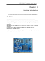
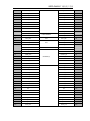
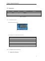
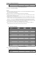
SEED-DIM3517 Hardware User Manual Documents Version and serial number SEED-DIM3517 hardware user’s manual Documents History Version History Author Updated date REV A Initial 田晓林 2010-7-30 Author Updated date Software Edition Version History SEED-DIM3517 Initial 2011-7 2010-10-22 AM3517 Solutions DSP Embedded Controller SEED-DIM3517 Hardware Users’ Manual SEED-DIM3517 Hardware Users’ Manual Version:A 2011.77 http://www.seeddsp.com IMPORTANT NOTICE SEED Electronic Technology Ltd reserves the right to make changes to its products or to discontinue any product or service without notice. Customers are advised to obtain the latest version of relevant information to verify that the data being relied on is current before placing orders. 4 SEED-DIM3517 Hardware Users’ Manual Preface Read This First Introduction This manual is the users’ guide for the SEED-DIM3517 hardware which based on AM3517 embedded multi-media system solutions. It described the hardware feature, principle and usage of SEED-DIM3517 in detail. Warranty The warranty period for all hardware and software products manufactured by SEED International is one year after shipment. SEED International guarantees free of charge repair or replacement for the manufacturer caused damaged products during warranty period. Software updates will be sent free of charge to the customer during warranty period. Trademarks SEED is trademark of SEED International. TI is trademark of Texas Instruments. If You Need Assistance … Web: http://www.seeddsp.com/eng Beijing Headquarter Address: Unit 1201, Pan-Pacific Plaza, No. 12A, South Street Zhongguancun, Haidian District, Beijing, P.R.China Zip: 100081 Tel: +86-010-62109765 Fax: +86-010-62109678 E-mail: [email protected] To help us Improve Our Documentation … If you would like to make suggestions or report errors in documentation, please email us. Be sure to include the following information that is on the title page: the full title of the book, the publication data, and the literature number. Email: [email protected] 6 SEED-DIM3517 Hardware Users’ Manual Contents Read This First Warranty Trademarks If You Need Assistance … To help us Improve Our Documentation … Chapter 1 1.1 Feature 1.2 Function Introduction Chapter 2 Board components 2.1 AM3517 Processor 2.1.1 AM3517 2.1.2 External Memory 2.2 SEED-DIM3517 Perpheral and Interface module 2.3 Power Module Chapter 3 Physical description 3.1 PCB layout 3.2 Connector 3.2.1 J4 emulation interface 3.2.2 J3 DIMM connector interface Appendix Appendix A: Board Size Appendix B reference material: SEED-DIM3517 Hardware Users’ Manual Chapter 1 Function Introduction This article mainly introduce the feature and system block diagram of SEED-DIM3517 1.1 Feature SEED-DIM3517 is an evaluation module based on AM3517 from Texas Instruments. AM3517 is a high-performance ARM Cortex-A8 microprocessor with speeds up to 600 MHz. The device offers 3D graphics acceleration while also supporting numerous peripherals, including DDR2, CAN, EMAC, and USB OTG PHY that are well suited for industrial applications. SEED-DIM3517 adopts DIMM design of “card Plug-in”, suitable for various of industrial applications. On-board resources: AM3517, NAND FLASH, DDR2, Power, EMAC PHY, JTAG…etc. DIMM Interface: 1.8V DIMM contactor. Peripherals: USB, VPFE, network port, 2D/3D graphics acceleration, HDQ\1-Wire, UART, I2C, SPI, MMC\SD\SDIO, McBSP, HECC, DSS, GPIO…etc. Chapter 1: Function Introduction Figure 1. SEED-DIM3517 Front View Figure 2. SEED-DIM3517 Back SEED-DIM3517 Hardware Resources: Processor:AM3517 NAND FLASH:K9F4G08U0A 4Gb DDR2:K4T1G164QE-HCE7 1Gb X 2 Ethernet port : PHY On-board RTC DIMM Connector interface(refer table 1) Power 1.2 Function Introduction System Block Diagram: 2 SEED-DIM3517 Hardware Users’ Manual Figure 1: SEED-DIM3517 Block Diagram SEED-DIM3517 硬件用户手册 Chapter 2 Board components This article mainly introduces the feature of the components on SEED-DIM3517 board. The hardware includes Professor, Interface and power. 2.1 AM3517 Processor 2.1.1 AM3517 AM3517/05 is a high-performance ARM Cortex-A8 microprocessor. The device offers 3D graphics acceleration while also supporting numerous peripherals, including DDR2, CAN, EMAC, and USB OTG PHY that are well suited for industrial applications. The CPU of SEED-DIM3517 is AM3517, it is a high-performance ARM Cortex-A8 microprocessor with speeds up to 600 MHz, with package of 491-pin BGA (17x17, 0.65mm pitch) for Non_invasive Debug [ZCN suffix]. AM3517 integrates various of peripherals, such as High-End CAN Controller and 10/100 Mbit Ethernet MAC (EMAC) etc, making it be of a help for designers to reduce the system development cost. The abundant interfaces facilitates the designers to do network and Serial Communication, suitable for Home and Industrial automation, Single Board Computers, and, it is available for graphic and high-end calculator functions when the power less than 1W. The processor 3.3V I/O reduce the system cost by canceling the requirement of level translator. AM3517 is the combiner of AM3505 with the PowerVR SGX Graphic engine, that enables the device to offer 3D graphics acceleration while also supporting numerous peripherals, including DDR2, CAN. The processing speed of graphic engine can reach 10Mpolygon per second, and support OpenGL ES 2.0. Image rotation, image enlarges or shrinks, even all in mouser actions can be implemented on the hardware, without consuming the basic frequency of ARM core Chapter 2 2.1.2 On-board components External Memory SEED-DIM3517 external memory: 4Gb NAND FLASH and 1Gb X 2 DDR2. NAND FLASH connects GPMC_NCS0, DDR2 connects SDRC_NCS0. 2.2 SEED-DIM3517 Peripheral and Interface module SEED-DIM3517 CPU board resources: RTC, JTAG, Ethernet PHY and standard DIMM connector. All the peripherals connections are expanded through DIMM connector. The detailed DIMM connector defined as following. Pin Signal 1 +5V 3 +5V 5 Function Signal Pin +5V 2 +5V 4 +5V +5V 6 7 GND GND 8 9 GND GND 10 11 GND GND 12 13 VBAT VBAT 14 15 NC \RST 16 17 NC GND 18 19 GND GND 20 21 USB0_DP RX+ 22 23 USB0_DM RX- 24 25 GND GND 26 27 USB1_DP TX+ 28 29 USB1_DM TX- 30 31 GND GND 32 33 USB0_ID LEDL- 34 35 USB0_DRVBUS LEDR- 36 37 USB0_VBUS GND 38 39 GND GND 40 MMC1_D4 42 POWER GND POWER RESET&NMI GND USB EMAC GND NC 41 CCDC_PCLK VIDEO IN&HECC 2 SEED-DIM3517 硬件用户手册 43 MMC1_D5 CAN_TXD 44 45 CAN_RXD NC 46 47 CCDC_D0 CCDC_D1 48 49 CCDC_D2 CCDC_D3 50 51 CCDC_D4 CCDC_D5 52 53 CCDC_D6 CCDC_D7 54 55 NC NC 56 57 NC NC 58 59 NC CCDC_FIELD 60 61 CCDC_HD CCDC_VD 62 63 UART3_TXD UART1_TXD 64 65 UART3_RXD UART1_RXD 66 67 I2C1_SDA I2C1_SCL 68 69 MCSPI1_CLK MCSPI1_SOMI 70 71 MCSPI1_CS1 MCSPI1_SIMO 72 73 GPIO_174 GPIO_176 74 75 GND GND 76 77 GPMC_CS0 NC 78 79 GPMC_CS1 NC 80 81 GPMC_CS2 UART2_TX 82 83 GPMC_CS4 UART2_RX 84 85 UART2_CTS NC 86 87 UART2_RTS NC 88 89 NC GPIO_3 90 91 GPIO_6 GPIO_56 92 93 GPIO_128 GPIO_186 94 95 MMC2_D7 MMC2_D6 96 97 MMC2_D5 MMC2_D4 98 99 MMC2_D3 MMC2_D2 100 101 MMC2_D1 MMC2_D0 102 103 MMC2_CMD MMC2_CLK 104 105 MMC1_D3 MMC1_D2 106 107 MMC1_D1 MMC1_D0 108 109 MMC1_CMD MMC1_CLK 110 111 NC NC 112 113 NC NC 114 115 NC NC 116 117 NC NC 118 119 TV_OUT1 32K_CLKOUT 120 121 SYS_BOOT5 SYS_BOOT2 122 123 SYS_BOOT3 SYS_BOOT0 124 125 GPIO_177 GPIO_170 126 UART1&UART3 I2C1 SPI1 GND EMAF&SD_0 Chapter 2 On-board components 127 GPIO_182 \VOUT_RST 128 129 GPIO_178 NC 130 131 GPIO_179 NC 132 133 GND NC 134 135 MCBSP3_CLKX MCBSP4_CLKX 136 137 MCBSP3_FSX MCBSP4_FSX 138 139 MCBSP3_DX MCBSP4_DX 140 141 MCBSP3_DR MCBSP4_DR 142 143 GND GND 144 145 NC NC 146 147 MCBSP2_DX NC 148 149 GND GND 150 151 NC NC 152 153 NC NC 154 155 MCBSP2_FSX GND 156 157 NC NC 158 159 MCBSP2_CLKX NC 160 161 NC NC 162 163 MCBSP2_DR NC 164 165 GND GND 166 167 NC NC 168 169 NC NC 170 171 GND GND 172 MCBSP3~4 GND MCBSP2 GND DSS 173 DSS_PCLK DSS_VSYNC 174 175 DSS_HSYNC DSS_ACBIAS 176 177 DSS_D15 DSS_D14 178 179 DSS_D13 DSS_D12 180 181 DSS_D11 DSS_D10 182 183 DSS_D9 DSS_D8 184 185 DSS_D7 DSS_D6 186 187 DSS_D5 DSS_D4 188 189 DSS_D3 DSS_D2 190 191 DSS_D1 DSS_D0 192 193 DSS_D17 DSS_D16 194 195 DSS_D19 DSS_D18 196 197 DSS_D21 DSS_D20 198 199 DSS_D23 管脚 信号 功能 DSS_D22 200 信号 管脚 Table 1. DIMM connector definition 4 SEED-DIM3517 硬件用户手册 2.3 Power Module The power on SEED-DIM3517 is TPS65023. It provides the board +1.2V, +3.3V, +1.8V and RTC power. From DIM pin input power: +5V Onboard Power: +3.3V,+1.8V,+3.3VA,+1.2VRTC,DDR_VREF,VBAT, +EMAC_1.8VA,+EMAC_1.8VPLL Main functions of these power: +3.3V:Work voltage for NAND, ENTHNET_PHY and IO voltage of AM3517. +1.8V:IO voltage of AM3517 and the work voltage of DDR2 +1.2VRTC:RTC voltage for AM3517 DDR_VREF:+0.9V Reference voltage of DDR2 VBAT: +3.3V, spare work voltage. +EMAC_1.8VA:work voltage of ENTHNET_PHY +EMAC_1.8VPLL:work voltage of ENTHNET_PHY SEED-DIM3517 Hardware Users’ Manual Chapter 3 Physical description 3.1 PCB layout SEED-DIM3517 front view J1 J2 J3 Figure 1. SEED-DIM3517 front view SEED-DIM3517 rear view: Figure 2.SEED-DIM3517 rear view 1 Chapter 3 physical description 3.2 Connector Name Type pin location function J1 button 5 top layer system reset J4 Connector 14 top layer AM3517 JTAG J3 Connector 200 top layer DIMM connector interface Table 1. Connector 3.2.1 J4 emulation interface JTAG emulator interface image: Figure 3. JTAG emulation interface J4 pin definition for JTAG emulation interface: Signal Pin Pin Signal TMS 1 2 TRST TDI 3 4 GND +3.3V 5 6 NC TDO 7 8 GND RSVD 9 10 GND TCK 11 12 GND EMU0 13 14 NC Table 2. JTAG pin definitions 3.2.2 J3 DIMM connector interface USB interface definition : 2 SEED-DIM3517 Hardware Users’ Manual Signal Pin Pin Signal USB0_DP 21 33 USB0_ID USB0_DM 23 35 USB0_DRVBUS GND 25 37 USB0_VBUS USB1_DM 29 27 USB1_DP GND 31 39 GND Table. USB pin definitions Description: USB USB (Universal Serial Bus) is an industry standard which defines the cables, connectors and protocols used for connection, communication and power supply between computers and electronic devices. USB was designed to standardize the connection of computer peripherals such as mice, keyboards, digital cameras, printers, portable media players, disk drives and network adapters to personal computers, both to communicate and to supply electric power. Up to now, there are three technology generations for USB: Generation 1: USB 1.0/1.1: Released in January 1996. Specified data rates of 12 Mbit/s Generation 2: USB 2.0, Released in April 2000, Added higher maximum bandwidth of 480 Mbit/s (60 MB/s) (now called "Hi-Speed"), compatible with USB 1.0/1.1 interface Generation 3: USB 3.0, USB 3.0 has transmission speeds of up to 5 Gbit/s, which is 10 times faster than USB2.0 (480 Mbit/s). USB 3.0 significantly reduces the time required for data transmission, reduces power consumption, and is downward compatible with USB 2.0. The USB 3.0 Promoter Group announced on 17 November 2008 that the specification of version 3.0 had been completed and had made the transition to the USB Implementers Forum (USB-IF), the managing body of USB specifications. This move effectively opened the specification to hardware developers for implementation in future products. USB On-The-Go, often abbreviated USB OTG, is a specification that allows for USB devices which would normally act as slaves, (e. g. digital audio players or mobile phones) to switch roles and become the host themselves. Description: USB0 connect USB OTG, this interface PHY is provided by AM3517. USB1 signal act as USB HOST interface, it offers PGY through chip USB3320QFN32. EMAC Interface definitions: Signal 3 Pin Pin Signal RX+ 22 32 GND RX- 24 34 LEDL- GND 26 36 LEDR- TX+ 28 38 GND Chapter 3 physical description TX- 30 40 GND Table 1. EMAC pin definitions Descriptions: network use RMII Details: RMII: Reduced Media Independent Interface, it is one of the standard Ethernet interfaces, less I/O transportation than MII. RMII uses two lines to transmit data, MII uses 4 lines to transmit data. MII/RMII is a kind of interface, for 10M link speed, the MII is 2.5M, RMII is 5M; for 100M link speed, MII is 25M, RMII is 50M. MII/RMII is used to transmit Ethernet package, the interface of MII/RMII is 4/2bit, codec will be available on UTP and optical fiber after serial-parallel conversation in the PHY of Ethernet, frame format: IEEE 802.3(10M)/IEEE 802.3u(100M)/IEEE 802.1q(VLAN). The frame format of Ethernet: Preamble+ Start of frame delimiter+ MAC destination+ MAC source+ Ethertype or length+data+ padding(optional)+32bitCRC If there exists vlan, you need to add vlan tag with 2 byte after “Ethertype or length”, in which, 12bit means vlan id, 4bit meant the priority of the data DSS interface definitions: Signal 管脚号 管脚号 信号 GND 172 171 GND DSS_D14 178 177 DSS_D15 DSS_D12 180 179 DSS_D13 DSS_D10 182 181 DSS_D11 DSS_D8 184 183 DSS_D9 DSS_D6 186 185 DSS_D7 DSS_D4 188 187 DSS_D5 DSS_D2 190 189 DSS_D3 DSS_D0 192 191 DSS_D1 DSS_D16 194 193 DSS_D17 DSS_D18 196 195 DSS_D19 DSS_D20 198 197 DSS_D21 DSS_D22 200 199 DSS_D23 DSS_VSYNC 174 173 DSS_PCLK DSS_ACBIAS 176 175 DSS_HSYNC Table 1. DSS PIN definitions Note:Support LCD and TV display UART interface definitions: Signal UART1_TXD Pin 64 Pin 63 Signal UART3_TXD 4 SEED-DIM3517 Hardware Users’ Manual UART1_RXD 66 65 UART3_RXD UART2_TX 82 85 UART2_CTS UART2_RX 84 87 UART2_RTS Table 1. UARTpin definitions Descriptions: UART (Universal Asynchronous Receiver/Transmitter), this BUS support bi-directional communication, realize Duplex Transmissions and data receiving. In the embedded design, UART is used to communicate with PC, including Monitoring debugger and other components, such as EEPROM. Note:The Initialization serial is UART3 in this core. MCBSP interface definitions: Signal Pin Pin Signal MCBSP4_CLKX 136 135 MCBSP3_CLKX MCBSP4_FSX 138 137 MCBSP3_FSX MCBSP4_DX 140 139 MCBSP3_DX MCBSP4_DR 142 141 MCBSP3_DR MCBSP2_DR 163 147 MCBSP2_DX MCBSP2_CLKX 159 155 MCBSP2_FSX Table 2. MCBSP Pin Definitions Description: McBSP is Multichannel Buffered Serial Port of Digital Signal Processors, produced by Texas Instruments. McBSP expands the function of the standard serial interface, so, it has the same basic function with standard serial interface. It can communicate with other serial devices such as DSP, encoder… Note:MCBSP doesn’t support A-LAW and U-LAW MCBSP2 can used as Audio data, Audio buffer and sidetone MCBSP3 can be used as Bluetooth speech data and sidestone MCBSP4 can be used as DBB speech data VIDEO IN interface definition: Signal Pin Pin CCDC_PCLK 41 61 CCDC_HD CCDC_D1 48 47 CCDC_D0 CCDC_D3 50 49 CCDC_D2 CCDC_D5 52 51 CCDC_D4 CCDC_D7 54 53 CCDC_D6 CCDC_VD 62 60 CCDC_FIELD Table 1. VIDEO IN pin definition Note:This interface is used to connect the camera MMC\SD interface definition: 5 Signal Chapter 3 physical description Signal Pin Pin Signal MMC2_D6 96 95 MMC2_D7 MMC2_D4 98 97 MMC2_D5 MMC2_D2 100 99 MMC2_D3 MMC2_D0 102 101 MMC2_D1 MMC2_CLK 104 103 MMC2_CMD MMC1_D2 106 105 MMC1_D3 MMC1_D0 108 107 MMC1_D1 MMC1_CLK 110 109 MMC1_CMD Table 2. MMC\SD PIN Definition Description:SD card(Secure Digital Memory Card)is a non-volatile memory card format developed by the SD Card Association for use in portable devices. The SD technology is used by more than 400 brands across dozens of product categories and more than 8,000 models, and is considered the de-facto industry standard. MultiMediaCard (MMC) is a flash memory memory card standard. Unveiled in 1997 by Siemens AG and SanDisk, it is based on Toshiba's NAND-based flash memory, and is therefore much smaller than earlier systems based on Intel NOR-based memory such as CompactFlash. MMC is about the size of a postage stamp: 24 mm × 32 mm × 1.4 mm. MMC originally used a 1-bit serial interface, but newer versions of the specification allow transfers of 4 or 8 bits at a time. It has been more or less superseded by SD (Secure Digital) card, but still sees significant use because MMCs can be used in most devices that support SD cards. A SDIO (Secure Digital Input Output) card is a combination of an SD card and an I/O device. This kind of combination is increasingly found in portable electronics devices. Hosts that support SDIO (typically PDAs like the Palm Treo, but occasionally laptops or mobile phones) can use small hosts designed for the SD form factor, like GPS receivers, Wi-Fi or Bluetooth adapters, modems, Ethernet adapters, barcode readers, IrDA adapters, FM radio tuners, TV tuners, RFID readers, digital cameras, or other mass storage media such as hard drives. Note:This core initializes SD as MMC\SD1. I2C interface definition : Signal I2C1_SCL Pin 68 Pin 67 Signal I2C1_SDA Table 3. I2C pin definition 6 SEED-DIM3517 Hardware Users’ Manual Description: I2C(Inter-Integrated Circuit) Inter-Integrated Circuit; generically referred to as "two-wire interface") is a multi-master serial single-ended computer bus invented by Philips that is used to attach low-speed peripherals to a motherboard, embedded system, or cellphone or other electronics. Since the mid 1990s several competitors (e.g. Siemens AG (later Infineon Technologies AG), NEC, Texas Instruments, STMicroelectronics (formerly SGS-Thomson), Motorola (later Freescale), Intersil, etc.) brought I²C products on the market, which are fully compatible with the NXP (formerly Philips' semiconductor division) I²C-system. As of October 10, 2006, no licensing fees are required to implement the I²C protocol. However, fees are still required to obtain I²C slave addresses allocated by NXP. SMBus, defined by Intel in 1995, is a subset of I²C that defines the protocols more strictly. One purpose of SMBus is to promote robustness and interoperability. Accordingly, modern I²C systems incorporate policies and rules from SMBus, sometimes supporting both I²C and SMBus with minimal re-configuration required. I²C uses only two bidirectional open-drain lines, Serial Data Line (SDA) and Serial Clock (SCL), pulled up with resistors. Typical voltages used are +5 V or +3.3 V although systems with other voltages are permitted. SPI Interface Definition: Signal Pin Pin Signal MCSPI1_SOMI 70 69 MCSPI1_CLK MCSPI1_SIMO 72 71 MCSPI1_CS1 GPIO_176 74 73 GPIO_174 Table 4. SPI pin definition Description: SPI:The Serial Peripheral Interface Bus or SPI (pronounced li ke "S.P.I." or "spy") bus is a synchronous serial data link standard named by Motorola that operates in full duplex mode. Devices communicate in master/sla ve mode where the master device initiates the data frame. Multiple slave devic es are allowed with individual slave select (chip select) lines. Sometimes SPI is called a "four-wire" serial bus, contrasting with three-, two-, and one-wire seri al buses. The SPI bus specifies four logic signals: SCLK: Serial Clock (output from master); MOSI; SIMO: Master Output, Slave Input (output from master); MISO; SOMI: Master Input, Slave Output (output from slave); SS: Slave Select (active low, output from master). Alternative naming conventions are also widely used: 7 Chapter 3 physical description SCK; CLK: Serial Clock (output from master) SDI; DI, DIN, SI: Serial Data In; Data In, Serial In SDO; DO, DOUT, SO: Serial Data Out; Data Out, Serial Out nCS, CS, CSB, CSN, nSS, STE: Chip Select, Slave Transmit Enable (active low, output from master) The SDI/SDO (DI/DO, SI/SO) convention requires that SDO on the master be connected to SDI on the slave, and vice-versa. Chip select polarity is rarely active high, although some notations (such as SS or CS instead of nSS or nCS) suggest otherwise. Note: GPIO_176 and MCSPI1_CS2 multiplexing; GPIO_174 and MCSPI1_CS0 multiplexing. 8 SEED-DIM3517 Hardware Users’ Manual Appendix Appendix A: Board Size DIM3517 board size: A-1 附录 Appendix B reference material: TI website http://focus.ti.com/docs/prod/folders/print/am3517.html Thanks This document is provided by the Research and Development department, we appreciate your comments and suggestions during your reading. This document will be updated on the website of SEED International Ltd, please check it at regular time. www.seeddsp.com/eng B-1