1
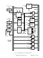
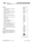
VME INTERFACE BOARD
This document describes the VME interface board Revision 7A dated 12/11/97, targeted to operating
Gen II controllers at full speed. The VME interface board is a 6U wide board that supports the full
32-bit address and data paths of the two connector VMEbus specification C.1. It continues the
evolution of two previous VME interface boards by incorporating their features, including support for
the faster fiber optic protocol of Gen II controllers, a fast FIFO data buffer on incoming data from the
timing board, a x2 faster DSP, more generalized support for VMEbus arbitration and interrupt generation, and a parallel data path for incoming data to be transmitted off-board.
A block diagram of the VME board is shown in Fig. 1, and a functional description of the board
follows. Part numbers are located on an accompanying parts drawing. The Motorola DSP56002 chip
U15 manages the board functions, serving as a communications node and address generator in direct
memory access (DMA) mode when the board is writing images to the VMEbus. It operates at an
internal clock speed of 64 MHz, using an internal phase locked loop (PLL) circuit that multiplies the
external VMEbus system clock of 16 MHz by four. It operates at an instruction processing speed of 32
MHz, or 31.25 nanosec per single word instruction. A OnCE connector is installed on the board for
use of the Motorola supplied in-circuit emulator as an aid to writing DSP code.
The VME interface board DSP transmits to the timing board using its internal synchronous serial
interface (SSI) at a speed of 4 MHz though the ODL50 series fiber optic transmitter U44. It receives
data from the timing board at a speed of 50 MHz (for Gen II controllers) or 40 MHz (for Gen I) from
the fiber optic serial receiver chip U34 using the clock recovery circuit U35 to generate a synchronous
clock, a serial to parallel shift register circuit implemented in PAL U29, and a first-in first-out (FIFO),
1k x 18 bit memory U30 and U36. The FIFO generates a DSP interrupt through the PAL U26 on line
B and de-asserts its empty flag that is monitored by the DSP if it has any contents. The DSP is
programmed to respond to interrupts when it expects commands and replies from the timing board,
and to monitor the empty or half full flags when image data is expected. The serial shift register PAL
U29 is currently does not support 18-bit image data.
A single memory-mapped VMEbus address is used to write commands to the DSP, determined by the
addressing jumpers JA1 - JA31. Long word (32-bit data) writes of either extended (32-bit address
space) or standard (24-bit address space) accesses to the address will causes the comparators U12,
U16, U18 and U20 and the PAL U14 to be asserted, generating a high going pulse on BRDSEL, in turn
generating a DSP interrupt level A signal with the flip flop U24A. The DSP jumps to an interrupt
service routine that reads the 24-bit data word that has been latched onto U32, U38 and U40 by the
RDCLK signal generated from BRDSEL and processes it as a command word. A write to the
command address +4 will cause a DSP reset signal to be generated, allowing the board to be reset by
software.
The DSP writes data to the VMEbus by writing the 32-bit VMEbus address and either 24- or 32-bit
data to latches that are asserted onto the VMEbus when the bus arbitration logic indicates that the bus
is available. The high address lines A16-A31 are written to the latches U21 and U23 only when they
change. The low address lines A01-A15 are written to the latches U17 and U19 and the data D0-D23
are written to the latches U25, U28 and U31 whenever the DSP writes to the VMEbus. Upon writing
to these latches the bus arbitration circuit (PAL U9 = C, U6 and U8) makes a request for ownership of
VMEbus Interface Board, pg. #1
Updated Jan. 13, 1999
BG#IN, AS, DTACK
VME BUS
ARBITRATION
DSP-WR
TO TIMING BOARD
BR#, BG#OUT
D0-D7
FIBER OPTIC
TRANSMITTER
# = 0 TO 3
VMEbus
IRQA
IRQB
VME
SSI
WRAM
DSP56002
PA
AM0-AM5
VME
PA
DSP-WR
A0-A14
A01-A15
VME
FROM
TIMING BOARD
RSTWDT
RESET
IRQ5
INTERRUPT
RQINTR
FIBER OPTIC
RECEIVER
D0-D23
PROCESSOR
D00-D07
VME
ADDRESS
A01-A31
32K X 24
SRAM
SHIFT
IRQA, BRDSEL
RDCOM
DECODE
REGISTER
1K X 16
FIFO
IRQB
RST-FIFO
RDFIFO
D0-D7
BOOT
ROM
A0-A15
Misc.
DSP
ADDRESS
DECODE
ADDRESS
BUS
A00 - A15
WRHADR
D00-D15
AM0-AM5
Misc.
RDFIFO
WRHADR
WRHDATA
RDCOM
RST-FIFO
RQINTR
DSP-WR
WRAM
RSTWDT
CE-ROM
A16-A31
VME
DSP-WR
DATA BUS
D00-D23
D00-D31
VME
BRDSEL
D00-D23
RDCOM
WRHDATA
D16-D31
VME
Fig. 1: Block diagram of the VME interface board.
VMEbus Interface Board, pg. #2
Updated Jan. 13, 1999
the bus. A bus request BR# is asserted (# = 0 to 3), the VMEbus bus arbiter responds with a bus grant
BG#, and the VME/I signal asserts the address and data onto the bus by enabling the outputs of the
latches. The address modifiers AM0 to AM5, and the control lines LWORD/I and WRITE/I are
asserted by a latch from values written previously by the DSP. The bus arbitration logic then asserts
the data and address strobe lines with U1, and terminates the bus cycle when DTACK/I low is
detected.
Two modes are implemented for efficient transfer of pixel data to the VMEbus. In both cases the pixel
data is written from the FIFOs directly to the latches in 32-bit per word mode, bypassing the DSP. One
mode, termed "rdfifo" in supporting signal names and DSP code, is activated whenever the range of
addresses Y:$8000 to Y:$FFFF is written to if when the address X:SETRDFIFO has been written to,
causing the PAL U7 to move two 16-bit words directly from the FIFO to the bus latches. The second
efficient way of writing image data is using the block transfer mode of VMEbus data transfer wherein
the addresses are not written to the bus on every data transfer, but only at the beginning of a block
transfer. This mode carries the "blt" designation in signal names and DSP code, following its VMEbus
name. The memory being written on the VMEbus to must support the block transfer mode to use this
mode.
Normally replies and commands are written as long words to the VMEbus by asserting LWORD/I.
However, only the 24 least significant bits are valid because that is the word length of the DSP. The
remaining 8 most significant bytes are written as all high, $FF, because they’re pulled up by the
VMEbus terminators. In image transfer mode the data is normally written in 32-bits format in one
transfer by writing the most significant 16-bits to the latches U37 and U39 prior to writing the least
16-bits to the normal VMEbus address space, and the entire 32-bit data word will be transferred in one
cycle over the VMEbus. In "rdfifo" and "blt" modes this is done in hardware by PALs, or the user can
do the same thing in software by writing to the appropriate registers.
Additional circuits complete the board. There is a memory bank of fast static RAM for buffering
incoming image data, 32k x 24-bits in size. There is a byte-wide ROM that contains boot code that is
loaded into the DSP after it exits the reset state, and can contain application code that is loaded on
command. The PAL U7 does the address decoding of all the DSP commands to effect the operations
discussed. Its memory map is given below. There is a watchdog timer and power monitor circuit U27
that resets the DSP if incoming power falls below 4.75 volts, and a jumper that can be set to reset the
DSP if the RSTWDT (reset watchdog timer) command is not executed at least once every 62.5
milliseconds. There is an interrupt processor circuit that will generate interrupts when the DSP issues
the appropriate command, and supports the generation of a byte-sized vector during interrupt
processing. The interrupt vector is specified by writing to the WRAM register. There is a connector
mounted on the front panel, CON24, that can be used to pass 16-bit image data from the output of the
FIFO to another board without passing through the VMEbus, with a handshaking flag to indicate when
data from a frame is being transferred.
DSP Memory Map and Control Bits Definitions
The DSP memory map follows, with an explanation of what each command does. Often users will
have to consult provided DSP source code and even the board schematic to fully comprehend the
instruction processing. The names of the operation are the same labels equated to the addresses in the
DSP source code.
VMEbus Interface Board, pg. #3
Updated Jan. 13, 1999
WRAM
X:$FFB0
RDFIFO
X:$FFB1
WRHADR
X:$FFB2
WRHDATA
X:$FFB3
RDCOM
X:$FFB4
RQINTR
RSTWDT
RSTFIFO
SELBLT
SETRDFIFO
CLRRDFIFO
X:$FFB5
X:$FFB6
X:$FFB7
X:$FFB8
X:$FFB9
X:$FFBA
Write address modifiers AM0-AM5, and VME control signals
WRITE/I and LWORD/I to a latch for assertion during
VMEbus bus master cycles. D0-D5 = AM0-AM5, D6 =
WRITE/I, D7 = LWORD/I and D16-D23 = interrupt vector.
Read 18-bit word from the FIFO. It contains image or
command/reply data from the timing board.
Write the high VME address bits A16-A31 to latches for
assertion onto the VMEbus on the next VMEbus master
cycle.
Write the DSP data lines D0-D15 on latches for assertion onto
the VMEbus data lines D16-D31 on the next bus master cycle
if a 32-bit data transaction has been requested by sending the
WORD-LENGTH bit of the DSP port B to 32-bit size.
Read incoming commands from the VMEbus data lines
D00-D23 to the DSP.
Write to this address to request VMEbus interrupt service.
Write to this address to reset the watchdog timer.
Write to this address to reset the FIFO.
Begin writing a block in block transfer mode
Select for operating the "rdfifo" automated mode
De-select the "rdfifo" mode
Memory read and writes operations to the memory spaces P:, X: and Y: get interpreted in different
ways depending on the address of the operation. Reads or writes to the following two memory ranges
cause either access to the VMEbus and a full arbitration and data transaction to occur, or an access to
the on-board EEPROM memory Y:$8000 to $FFFF Read or write to or from the VMEbus.
P:$8000 to $FFFF Read or write to on-board EEPROM memory.
A fast static RAM memory bank (SRAM) that is 32k x 24 bits in size is located on the board, and split
into three separate memory spaces. P: and X: operations each access 8k segments of the memory, and
Y: operations access the remaining 16k segment. SRAM in inaccessible for P: address below $200 and
X: or Y: addresses below $100 because these memory operations access internal DSP memory instead.
P:$200 to $1FFF
X:$100 to $1FFF
Y:$100 to $3FFF
Read or write to or from external SRAM memory.
Read or write to or from external SRAM memory.
Read or write to or from external SRAM memory.
The following bits are controlled directly by the DSP port B. The are configured as general purpose
I/O pins, variously as inputs or outputs, and used to control various board functions. They are
controlled by the following programmeable pins -
VMEbus Interface Board, pg. #4
Updated Jan. 13, 1999
Bit #
Name
0
BLT
1
REM_RST
I/O
Output
Output
2
MODE
Output
3
4
AUX1
H4
Output
5
H5
Output
6
7
AUX5
REQBUS/I
Output
8
9
AUX2
AUX3
Output
Input
10
11
12
13
AUX4
HASBUS
Input
WORD-LENGTH Output
DONEVME Input
14
HF/I
Input
Function
Set to enable block transfer mode to the VMEbus.
Set to reset the remote circuit board. It is mapped to pin #17 of
the external data connector CON24.
Set to receive 32-bit command/reply data and clear to receive
16-bit image data. 18-bit image data is not supported.
Unused.
Value of data strobe signal DS0/I asserted on VMEbus cycles. It
is asserted as a zero, indicating 32-bit data transfers.
Value of data strobe signal DS1/I asserted on VMEbus cycles. It
is asserted as a zero, indicating 32-bit data transfers.
Unused.
Clear to request VME bus ownership. This can be used to gain
VME bus mastership ahead of a block of transfers for
improved speed compared to requesting the bus on every
transfer.
Can be used to generate an FYNC signal from the DSP.
Connected to signal FSYNC inside PAL U29 for the DSP to
monitor it. See the adaptive optics port discussion below.
Unused.
Set to indicate that the board is the current VMEbus master.
Set to write 32-bit data words to the VMEbus, clear for 24-bit.
Set to indicate that the board is finished with the VMEbus transaction and available for the next one.
Cleared to indicate that the input FIFO is half full.
Continuing on, the following bits are controlled by the DSP, but from port C, available by reading or
writing from or to the address X:$FFE5 = X:PCD. As of this writing DSP code has not been written to
implement the bus arbitration options other than the prioritized, jumper selected one.
0
BCLR
Input
Routed from VMEbus arbitration signal BCLR for implementation of Round Robin bus arbitration protocol.
1
BR0
Input
Routed from VMEbus arbitration signal BR0 for implementation
of FAIR bus arbitration protocol.
2
BR1
Input
Routed from VMEbus arbitration signal BR1 for implementation
of FAIR bus arbitration protocol.
3
BR2
Input
Routed from VMEbus arbitration signal BR2 for implementation
of FAIR bus arbitration protocol.
4
BR3
Input
Routed from VMEbus arbitration signal BR3 for implementation
of FAIR bus arbitration protocol.
5
Unused
6
Serial transmitter clock, not general purpose I/O.
7
EF/I
Input
Cleared to indicate that the input FIFO is empty.
8
Serial transmitter data, not general purpose I/O.
VMEbus Interface Board, pg. #5
Updated Jan. 13, 1999
15K SIP
VMEbus command address A01-A31.
A jumper installed clears the address bit to a zero.
The default address indicated is $1a000000.
M0
M1
M2
L0
L1
L2
N
15K SIP
IACK0
IACK1
IACK2
15K SIP
ADR sets the Address Modifier mode for processing incoming VMEbus commands.
M0-M2, L0-L2 and N set the speed of the fiber optic receiver.
The default shown is 50 MHz. Other speeds are shown in the text.
IACK0-IACK2 sets the interrupt acknowledge level processed by the board,
digitally encoded. IACK0 maps to A03 and IACK2 maps to A01, a silk screen bug.
Interrupt request level, 0 to 7. Only one jumper should be installed, and it must
match the acknowledge level of jumpers IACK0-IACK2.
Bus request and grant levels, allowing a choice of levels 0 to 3. The default
level 3 is shown.
These are located right above the ROM socket.
EEPROM (28C256), write disabled
EEPROM, write enabled
UV ROM (27C256)
The reset watch dog timer jumper is located to the right of the DSP.
This selection disables the watch dog timer.
This selection enables the watch dog timer, requiring a RSTWDT instruction
at least every 62.5 milliseconds.
When installed this jumper selects the serial receiver
for operation with Gen I controllers.
Jumper Settings
There are many jumpers on the board to select operating modes and addresses. The default settings are
as follows Command address = $1a000000
Fiber optic speed = 50 MHz
Address modifiers = $
Interrupt level = 7
Bus request level = 3
ROM = write disabled EEPROM
Watch dog timer = disabled
Reset address = command address + 4
VMEbus Interface Board, pg. #6
Updated Jan. 13, 1999
Generation II = selected
The figure shows the schematics of the jumper blocks with the default jumper settings. The command
address is determined by four rows of jumpers, labeled in the silk screen on the board by the upper and
lower address bit number on each end. Installing a jumper selects a zero for the address bit. The
VMEbus specification requires that address modifier lines AM0-AM5 be set on all bus transfers. The
jumper labeled ADR near the PAL U14 selects between the three following address modes
Jumper on the top two pins: AM = $39, Standard (24-bit) non-priviledged data access
Jumper on the bottom two pins: AM = $09, Extended (32-bit) non-priviledged data access
No jumper installed: AM = $09 or $39, either standard or extended non-priviledged data access
A group of jumpers located behind the fiber optic components selects the speed of the fiber optic
receiver, the interrupt acknowledge level and the address modifier. The jumper settings for three
fiber optic speeds are shown in the table below.
M0
M1
M2
L0
L1
L2
N
4 MHz (self-test)
open
open
jumper
open
open
jumper
jumper
40 MHz (Gen I) 50 MHz (default)
jumper
jumper
jumper
jumper
jumper
jumper
open
jumper
jumper
jumper
jumper
jumper
open
open
The default setting is 50 MHz, which is the frequency of the timing board transmitter on Generation II
controllers. The 4 MHz setting is used to exercise the interface board in a loopback self-test that maps
the 4 MHz transmitter of the board directly to the receiver. The 4 MHz jumper setting may be of
interest if a self-test feature is ever implemented since the fiber optic transmitter speed is 4 MHz. The
40 MHz is used to operate Generation I timing board serial transmitter, though the serial receiver PAL
does not now support this.
Interrupt request levels are selected by the jumper block IRQ0 to IRQ7 located near the VMEbus
connectors. Installing a jumper simply selects that level, with level 7 being the highest priority. The
interrupt acknowledge level from 0 to 7 is selected by the three jumpers IACK0 to IACK2 located in
the fiber optic receiver area, binary encoded. The interrupt request and acknowledge levels must be set
to be the same number for normal interrupt processing.Installing a jumper represents a zero (0) and no
jumper represents a one (1). But there is a bug in the silk screen labelling on the board wherein the
IACK0 and IACK2 labels have been switched. IACK2 is the least significant bit and IACK0 is the
most significatn bit. The default setting for the board is for interrupt level 7, so a jumper is placed on
the IRQ7 line and no jumpers are placed on IACK0-2.
Mastership of the bus must first be established for the interface board to transfer data over the
VMEbus. This is done by requesting the bus at one of four priority levels, selected by jumpering one
VMEbus Interface Board, pg. #7
Updated Jan. 13, 1999
of the levels BR0 to BR3. For proper operation, the same level must be selected in the bus grant
jumper block by placing jumpers two jumpers, one on the left side and one on the right side of the bus
grant jumper at the desired bus request level. Jumpers must also be placed on the center pair of jumper
posts for the other request levels to pass the unwanted bus grant signals through the board onto other
boards in the system that may need them.
Three options exist with the ROM memory part located below the fiber optic components. These are
to install an electrically erasable ROM that is write disabled, the same part but write enabled, and a UV
erasable, read only ROM. The jumper settings for these three cases is shown in the figure.
A reset watch dog timer circuit is installed to reset and reboot the board, including the DSP, if the
software is not executing properly. To enable the watchdog timer circuit a jumper needs to be placed
on the right hand side of the little RSTWDT block below PAL U7, and instructions must be placed in
the DSP code to insure that the corresponding DSP memory location is written to at least every 62.5
milliseconds.
Finally, a jumper below the DSP can be installed to select Generation I serial receiver data formats,
although the serial receiver PAL to do this has not yet been developed at the time of this writing. Users
desiring this feature should contact the designers for help.
Adaptive Optics Port
A 24-pin IDC connector (male) J4 is installed to serve as a parallel image data port that can be
connected directly to image processing hardware, and is called the ’C80 data port since it was
designed to interface to thye Texas Instruments ’C80 family of DSPs. The pinout of the connector is
given below 1
3
5
7
9
11
13
15
17
19
21
23
D06
D04
D02
D00
D14
D12
D10
D08
REM-RST
FIFORD
EF*
FSYNC
2
4
6
8
10
12
14
16
18
20
22
24
D07
D05
D03
D01
D15
D13
D11
D09
No connection
GND
GND
GND
The lines D00 to D15 contain image data transmitted over the fiber optics data link from the timing
board after they have been bufferred by the FIFO on the VME board.
VMEbus Interface Board, pg. #8
Updated Jan. 13, 1999
REM-RST
FIFORD
EF*
FSYNC
An output signal from the DSP bit D1 of the parallel port B used for initializing
the hardware connected to the ’C80 port.
A low true signal input to the VME board routed to the RD* pin of the FIFO.
The FIFOs are generic type 7202 1k word deep devices with 12 nanosec access
times, requiring that the FIFORD signal be at least this long.
A low true output from the VME board that indicates that the FIFO is empty.
Output from the VME board, this signal will equal the value of the incoming
serial data word bit D0 if D15 = 1 and the AUX2 bit #8 of parallel port B equals
1. It is intended to be as a synchronization signal to that is high when image data
is being transmitted.
Note that 16-bit image data is processed by the port if the VME board is not set to generate the frame
sync signal FSYNC. If a frame sync is needed then the most significant bit of the image D15 is used
to encode the frame sync information and only 15-bit image data can be transmitted.
To effectively use this port capability with the timing board its PALs U12 and U17 must be revision
4.1 or later. All timing board manufactured and delivered on or after May 15, 1998 have this or later
revision PALs, so users of boards manufactured earlier than that date should request current revision
PALs if they want to use this capability. The detailed functionality of the timing board PALs is
described in the timing board user’s manual, and DSP code is given below to operate both the timing
and VME boards in this mode.
In the following code segments PBDDR = $FFE2 is the address of the port B data direction address
register, and PBD = $FFE4 is its data register. The VME board DSP code needs to initilize the Port B
bit #8 to an output, as follows BSET
#8,X:PBDDR
; Set bit #8 - AUX2 to an output
Similarly, in the timing board readout code, two lines need to be set to outputs and initialized FD15 EQU
FMODE EQU
BSET
BSET
BSET
10
12
#FD15,X:PBDDR
#FMODE,X:PBDDR
#FMODE,X:PBD
; Value of forced data bit 15
; Forced data bit 15 mode if set
; Set this bit to an output
; Set this bit to an output
; Put board in forced bit mode
The RDCCD routine should set SYNC high at the beginning of the frame readout BSET
MOVEP
BCLR
#FD15,X:PBD
#>1,Y:WRFO
#FD15,X:PBD
; Force D15 = 1
; Transmit D0 = 1 to the VME board
; Force D15 = 0
and then clear SYNC at the end of the frame readout VMEbus Interface Board, pg. #9
Updated Jan. 13, 1999
REP
NOP
BSET
MOVEP
BCLR
REP
NOP
#20
; Wait for the last pixel transmission
#FD15,X:PBD
#0,Y:WRFO
#FD15,X:PBD
#10
; Force D15 = 1
; Transmit D0 = 0 to the VME board
; Force D15 = 0
; Wait for the last pixel transmission
and possibly put the timing board in non-forced data bit D15 mode if images are not to be transmitted
continuously BCLR
#FMODE,X:PBD
; Take the board out of forced bit mode
Application commands
The DSP software chapter describes the commands that are located in the "vmeboot" program that is
loaded from EEPROM after the DSP is reset, and are in common with the other DSP boards in the
system. These are the read and write memory commands (RDM and WRM), the test data link
command (TDL) and the load application command (LDA). Every command to the interface board is
prefaced with a header word, consisting of a source byte, a destination byte and a number of
commands words byte. The interface board is number one, as determined by the DSP boot code. All
commands with a one for the destination byte are processed by the VME interface board; commands
with destination bytes of two or three are passed to the timing board through the fiber optic data link,
and destination bytes of zero are passed to the host computer through the VMEbus. Headers with
destination bytes outside this range are ignored, as processing continues on to the next word in the
command string. Replies are made to the VMEbus by writing to an address space specified with the
Set Reply Address (’SRA’) command, which is of the form
$000104
’SRA’
high 16-bits of address
low 16-bits of address
Replies to commands will always consist of a header containing source, destination and command
length bytes, followed by at least one word that may contain data or ASCII codes. The SRA command
will generate a reply to the VMEbus starting at the address specified in its argument list, and the next
command reply will start eight bytes away. The reply to many commands is a simple ASCII ’DON’
meaning that the command was executed successfully, or an ’ERR’ meaning that it was not successful.
The replies will be written starting at the address indicated by ERA and incremented over a 128 byte
range, after which it will restart at the address specified by SRA. Users may either use this circular
addressing scheme or may issue frequent SRA commands to keep the address from circling. An
addressing limitation is that the 128 byte reply area must not cross a 64k byte VMEbus address
boundary. All replies also result in an optional interrupt being requested by the interface board so the
device driver can efficiently process the replies. A timeout feature writes a ’TIM’ reply if a complete
command is not received in 50 milliseconds, controlled by the TIMEOUT constant.
VMEbus Interface Board, pg. #10
Updated Jan. 13, 1999
Several commands are implemented in the application code "vme1.asm’. The RDC and ABR
commands are also implemented by the timing board, but execute differently. These commands are as
follows:
RDC
ABR
Read CCD - Set up interface board to read out CCD. All further data from the
timing or utility boards will be interpreted as 16-bit/pixel image data.
Switching back to 32-bit command/reply mode will occur after the VME
interface board has counted the number NPXLS of data points.
Abort Readout, and place interface board in command processing mode. Issue
an abort readout command to the timing board.
SRA is a boot command, and the remaining ones are application commands. A single word is encoded
to contain status information about the board processing state. It is located at the data memory word
X:0, which can be read or written from the host with RDM or WRM command.
Host computer command:
Interface board reply:
$000103
$010002
’RDM’
value
$200000
The following bits are defined for X:STATUS = X:0 bit 0 Set by the DSP program if it is in readout mode, cleared if in command processing mode.
bit 2 Set if an SRA command has been executed since the last DSP boot. If not then replies will not
be generated.
bit 3 Set if a command being processed was received from the timing board, cleared if it came from
the host computer. This is used internally for command processing.
An options word defined at X:1 is used to set firmware execution options. It can be written to or read
with the commands:
Host computer command:
Host computer command:
Interface board reply:
$000104
$000103
$010002
’WRM’
’RDM’
value
$200001
$200001
value
The following bits are defined for X:OPTIONS = X:1 bit 1
Set to require that the interface board request VMEbus interrupt service after
each command reply and after the all the images have all been transferred.
Default is no interrupts.
bit 2
Set to require that the DSP translate the incoming 16-bit straight binary image
data to twos complement format for compatibility with the FITS. It will convert
data over the range from [0 to 64k] -> [-32k to +32k]. Default is no conversion.
"vme1" Application Program # 1
This application reads from a single readout, being the simplest of the applications. It can be
VMEbus Interface Board, pg. #11
Updated Jan. 13, 1999
downloaded from the host computer or loaded from on-board ROM memory with the command ’LDA
1’. The number of pixels to be read is stored in the DSP memory location Y:1. However, if the number
of pixels to be read exceeds the 24-bit range of the DSP data values (16 Mpixels) then the number of
columns to be read can be written to Y:2 and the number of rows to Y:3, with the product of the two
numbers being calculated by the DSP to determine the number of pixels to be read up to 8 Gpixels. If
the number of pixels is non-zero then it will determine the number of pixels to be read. The starting
VMEbus address where the image data will be written to is set by the host computer by writing to a
table in DSP memory. The address lines A0-A9 must be zero for this program to work properly, that
is, the image buffer must start on a 1024 byte (1k) boundary. This table is not overwritten by the DSP
program, so only needs to be written only once. The table begins at Y:VME_TBL = Y:$40 and a
contains a pair of addresses containing the high and low 16-bits of the 32-bit VMEbus address. A
shadow buffer is maintained by the DSP starting at address Y:$60 that contains the current addresses
being written to by the DSP, and is initialized to the starting address table at the beginning of readout.
For setting this up the host computer should issue the commands $000104
$000104
$000104
$000104
$000104
’WRM’
’WRM’
’WRM’
’WRM’
’WRM’
$400040
$400041
$400001
$400002
$400003
highest 16-bits of VMEbus address
lowest 16-bits of VMEbus address
NPXLS - Total number of pixels to be read
NCOLS - Number of columns to be read
NROWS - Number of rows to be read
Readout will begin once the interface board receives an RDC command. The interface board will be
placed in readout mode whereby any data received from the timing board over the fast fiber optic data
link will be interpreted as image data until the desired number of pixels is received. Image data is
allowed to accumulate in the image FIFO buffer in 512 pixel blocks, then transferred a block at time
as quickly as possible over the VME bus. The image data will be written back to the VMEbus at 16
bits per pixel in 32-bit words, setting the VMEbus control lines DS0 = DS1 = LWORD = 0, except for
the last portion of the image that is less than or equal in size to half the FIFO buffer (512 pixels) which
gets written to the VMEbus in 16-bit words. The number of pixels received since the start of readout
can be read from the location Y:NBLOCKS = Y:4, as follows:
$000104
’RDM’
$400004
NBLOCKS - Number of 512-pixel blocks
read so far
Processing this command interrupts the processing of image data with a fair amount of overhead, so
should not be executed too often in high data rate applications.
As of this writing the abort command ABR has not been implemented.
VMEbus Interface Board, pg. #12
Updated Jan. 13, 1999