1
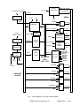
the bus. A bus request BR# is asserted (# = 0 to 3), the VMEbus bus arbiter responds with a bus grant
BG#, and the VME/I signal asserts the address and data onto the bus by enabling the outputs of the
latches. The address modifiers AM0 to AM5, and the control lines LWORD/I and WRITE/I are
asserted by a latch from values written previously by the DSP. The bus arbitration logic then asserts
the data and address strobe lines with U1, and terminates the bus cycle when DTACK/I low is
detected.
Two modes are implemented for efficient transfer of pixel data to the VMEbus. In both cases the pixel
data is written from the FIFOs directly to the latches in 32-bit per word mode, bypassing the DSP. One
mode, termed "rdfifo" in supporting signal names and DSP code, is activated whenever the range of
addresses Y:$8000 to Y:$FFFF is written to if when the address X:SETRDFIFO has been written to,
causing the PAL U7 to move two 16-bit words directly from the FIFO to the bus latches. The second
efficient way of writing image data is using the block transfer mode of VMEbus data transfer wherein
the addresses are not written to the bus on every data transfer, but only at the beginning of a block
transfer. This mode carries the "blt" designation in signal names and DSP code, following its VMEbus
name. The memory being written on the VMEbus to must support the block transfer mode to use this
mode.
Normally replies and commands are written as long words to the VMEbus by asserting LWORD/I.
However, only the 24 least significant bits are valid because that is the word length of the DSP. The
remaining 8 most significant bytes are written as all high, $FF, because they’re pulled up by the
VMEbus terminators. In image transfer mode the data is normally written in 32-bits format in one
transfer by writing the most significant 16-bits to the latches U37 and U39 prior to writing the least
16-bits to the normal VMEbus address space, and the entire 32-bit data word will be transferred in one
cycle over the VMEbus. In "rdfifo" and "blt" modes this is done in hardware by PALs, or the user can
do the same thing in software by writing to the appropriate registers.
Additional circuits complete the board. There is a memory bank of fast static RAM for buffering
incoming image data, 32k x 24-bits in size. There is a byte-wide ROM that contains boot code that is
loaded into the DSP after it exits the reset state, and can contain application code that is loaded on
command. The PAL U7 does the address decoding of all the DSP commands to effect the operations
discussed. Its memory map is given below. There is a watchdog timer and power monitor circuit U27
that resets the DSP if incoming power falls below 4.75 volts, and a jumper that can be set to reset the
DSP if the RSTWDT (reset watchdog timer) command is not executed at least once every 62.5
milliseconds. There is an interrupt processor circuit that will generate interrupts when the DSP issues
the appropriate command, and supports the generation of a byte-sized vector during interrupt
processing. The interrupt vector is specified by writing to the WRAM register. There is a connector
mounted on the front panel, CON24, that can be used to pass 16-bit image data from the output of the
FIFO to another board without passing through the VMEbus, with a handshaking flag to indicate when
data from a frame is being transferred.
DSP Memory Map and Control Bits Definitions
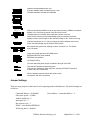
The DSP memory map follows, with an explanation of what each command does. Often users will
have to consult provided DSP source code and even the board schematic to fully comprehend the
instruction processing. The names of the operation are the same labels equated to the addresses in the
DSP source code.
VMEbus Interface Board, pg. #3
Updated Jan. 13, 1999