1
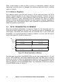
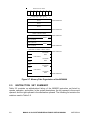
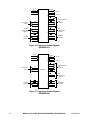
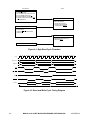
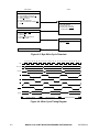
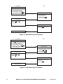
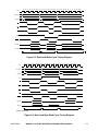
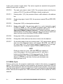
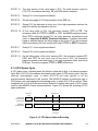
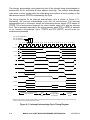
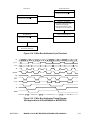
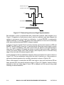
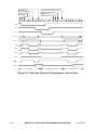
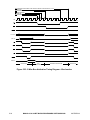
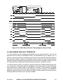
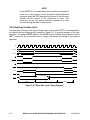
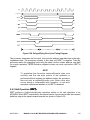
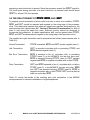
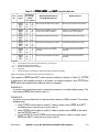
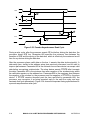
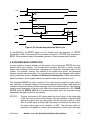
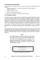
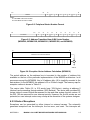
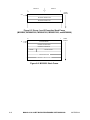
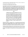
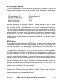
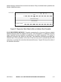
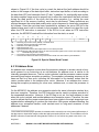
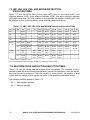
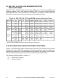
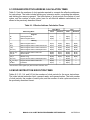
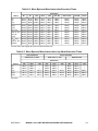
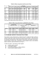
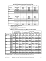
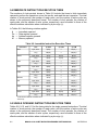
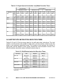
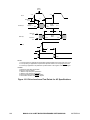
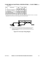
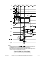
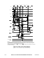
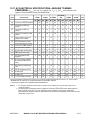
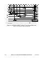
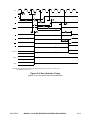
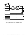
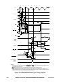
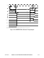
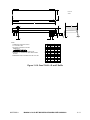
S0
S1
S2
S3
S4
S5
S6
S7
S0
CLOCK
6
9
.
ADDR
AS
UDS/LDS
18
R/W
47
DTACK
23
53
DATA
Figure 5-36. Synchronous Write Cycle
A key consideration when designing in a synchronous environment is the timing for the
assertion of DTACK and BERR by an external device. To properly use external inputs, the
processor must synchronize these signals to the internal clock. The processor must
sample the external signal, which has no defined phase relationship to the CPU clock,
which may be changing at sampling time, and must determine whether to consider the
signal high or low during the succeeding clock period. Successful synchronization requires
that the internal machine receives a valid logic level (not a metastable signal), whether the
input is high, low, or in transition. Metastable signals propagating through synchronous
machines can produce unpredictable operation.
Figure 5-37 is a conceptual representation of the input synchronizers used by the M68000
Family processors. The input latches allow the input to propagate through to the output
when E is high. When low, E latches the input. The three latches require one cycle of CLK
to synchronize an external signal. The high-gain characteristics of the devices comprising
the latches quickly resolve a marginal signal into a valid state.
EXT
SIGNAL
D
G
Q
D
G
Q
D
Q
INT
SIGNAL
G
CLK
CLK
Figure 5-37. Input Synchronizers
5-38
M68000 8-/16-/32-BIT MICROPROCESSORS USER'S MANUAL
MOTOROLA


![CPU32 Reference Manual [330 pages!]](http://vs1.manualzilla.com/store/data/005686632_1-79fc9549061344d5fca8ab86e2038cb9-150x150.png)