1
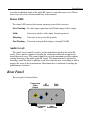
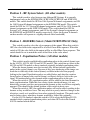
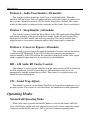
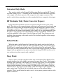
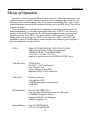
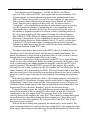
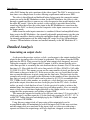
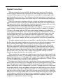
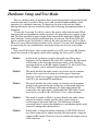
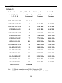
Standards Converter
with
RF Modulator
Model’s SCRF
User and Technical
Manual
Copyright 2006-9 Aurora Design LLC.
Revision 2.2
6 August, 2009
All specifications subject to change
www.tech-retro.com
Introduction
Introduction
This manual covers the operation and technical aspects of the Single-Standard
Converter with RF Modulator. The Converter is designed to accept an NTSC or
PAL/SECAM video signal and convert to one of several different output standards
depending on the model. The converted video is sent to the built-in RF Modulator,
along with the audio, and to a composite video output connector.
Features
• Compact, low power, surface mount design
• Front panel Status LED
• Internal user switch selectable options control
• Flexible built-in RF Modulator:
- Up to 30 selectable carrier frequencies
- Programmable between 30-880MHz (actual channels vary by model)
- Supports positive/negative video and AM/FM audio modulation schemes
• Converter bypass mode for use as stand alone RF Modulator
• Extremely stable output: +/- 3% levels, +/- 50ppm timing
• Output clock line locked to input clock for perfect conversions
• 10 bit video D/A for greater than 54dB dynamic range
• 4Mb FLASH Image Memory for storing a custom image
• 100K gate equivalent FieldProgrammableGateArray (250K on SCRF405A-NTSC)
• EEPROM memory for FPGA firmware, field upgradeable
• Extremely accurate algorithms used for conversions:
- Three line interpolation on all standards
- All internal calculations done to a minimum 12 bit precision
• Unique partial-field memory for stable output syncs
• Externally adjustable RF channel and audio modulation depth control
• Automatic Sleep Mode for low power standby operation
• Versatile I/O:
- Composite Video Input (NTSC/PAL, 1Vpp, 75 ohm)
- Composite Video Output (various standards depending on model, 1Vpp, 75 ohm)
- Stereo Audio Inputs (-10dBV nominal, 0.2Vpp-5Vpp, 20k ohm)
- RF Output (76dBμV, 75 ohm, approx. 6mV)
- DC power (7-14Vdc, 250ma)
3
Introduction
Front Panel
The front panel is shown below:
Composite
Video
Input
Left
Audio
Input
Status
LED
Right
Audio
Input
Audio
Level
Composite Video Input:
The Composite video input signal required depends on the operating mode and
model of the converter. If the converter is enabled (not bypassed), then a video
source conforming to the NTSC or PAL/SECAM video standards must be supplied
to the Composite (RCA or BNC) input connector. An NTSC source must be used
with 30 fps models and a PAL/SECAM source must be used with 25fps models. The
converter will use this video signal to convert to the model’s output standard. For
example, the SCRF405A converter with convert a PAL/SECAM source to 405/25i
video. Connecting a video signal not conforming to the NTSC or PAL video
standards will result in erratic operation in this mode.
If the converter is set to bypassed, then the video signal on this connector is sent
to the modulator with no signal processing, other than an audio trap filter. Any video
signal can be supplied in this mode, although it is the users responsibility to verify this
video signal to obtain the desired result from the modulator.
Audio Inputs:
Two RCA connectors are provided for audio input. The two connectors are
summed internally into a mono signal that is fed to the RF modulator. If only a mono
source is available, it can be connected to either of the audio input connectors, or
both through a “Y” cable if higher input gain is required. The inputs can accept a
wide range of audio input levels, but are designed to work optimally with standard,
consumer level -10dBV audio signals. Due to the variance of audio output levels from
many devices however, an audio input gain control is provided which allows the user
4
Introduction
to set the modulation depth of the audio RF carrier to suite the source level. Please
refer to Specifications sections found later in this manual.
Status LED:
The status LED conveys the current operating state of the converter.
Slow Flashing: No video input signal detected. Default image will be output.
Solid:
Converter locked to video input. Normal operation.
Pulsating:
Converter in low power Sleep mode.
Fast Flashing: Converter storing default image to internal FLASH
Audio Level:
The Audio Level control is used to set the modulation depth of the audio RF
carrier. This control is required to handle the variations in the audio output levels
from different devices. This control should be set to the maximum possible without
causing distortion of the audio in the RF signal. The potentiometer is adjusted by
inserting a small flat blade or phillips screw driver into the hole, and turning it until it
engages the rotor of the potentiometer. Maximum drive is obtained by turning the
potentiometer clockwise.
Rear Panel
The rear panel is shown below:
Composite
Video
Output
RF
Output
9Vdc
Input
RF Channel
User
Select
Pushbutton
5
Introduction
Composite Video Output:
This RCA or BNC connector provides the video output from the converter. This
output should terminate into a 75 ohm load. This output is only valid when the
converter is not set to bypass mode. If the converter is set to bypass mode, no signal
will be present at this output. For complete information about the characteristics of
this output, please refer to the Specifications section found later in this manual.
RF Channel Select:
The RF Channel Select control is used to select the output frequency, or channel,
of the RF output. The specific frequency or channel for each position is unique to the
model of converter, and can be found on the bottom label of the converter, and in the
Supported RF Systems section found later in this manual. When the switch is set to
‘0’, the RF modulator is disabled and put into a low power state. In this mode, the
unit will still output a converted video signal on the composite output connector. This
control is adjusted by inserting a small flat blade or phillips screw driver into the hole,
and engaging the slots in the switch.
RF Output:
This F connector provides the RF output from the modulator. This output should
terminate into a 75 ohm load. It should only be used to connect directly to the
antenna terminals of a television set, and never be used for broadcast purposes. For
complete information about the characteristics of this output, please refer to the
Specifications section found later in this manual.
User Pushbutton:
The User Pushbutton is used to store a default image into the internal FLASH
memory. On the SCRF525M-SC, it is additionally used to control the color phasing
of the output, rotating by one field each time the button is pushed momentarily.
To store a default image, the converter must be in it’s normal operating mode,
with a valid video input connected, and a Solid Status LED. If a valid video input is
not connected, the button will have no effect. With a stable, stationary video input
applied, the user button may be pressed and held for 2 seconds by inserting a paper
clip, or other small tool into the hole in the back of the unit. The Status LED will
begin to flash quickly, indicating storing of the image FLASH is taking place. This
process can take about 15 seconds, and the video signal must not be disturbed during
this process. Once the image is stored, the Status LED will return to solid.
Once an image is stored, whenever there is no video input connected to the unit,
the default image stored in the FLASH will be outputted.
6
Introduction
Caution! Because of the nature of the partial-field memory contained in this unit,
the default image is stored in bands of several lines at a time. If the connected video is
not stationary during the storing process, the resulting image will be distorted. The
best way to provide a stationary image for storing is to use the output from a
computer video card, or a DVD/PVR player in pause. A typical VCR without a TBC
in pause is not suitable for this use.
Power:
The converter requires a power source of between 7.0 and 14 volts DC at 250
mA. A 9 volt DC power supply is recommended to reduce power consumption.
Voltages over 16 volts will damage the unit. The unit has a reverse polarity diode in
series with the input, so it will not be damaged by reversal of polarity. The unit uses a
standard 2.1mm X 5.5mm, center positive, coaxial power connector as found on
most consumer electronic equipment.
Internal Options
The internal Options switch and AM Audio RF Carrier control are shown below:
1 2 3 4 5 6
ON
R9
R10
U2
R45
C32
R4
U7
J5
C66
AM Audio
Carrier
Adjust
Option
Switch
Programing
Port
R3
U1
Back of unit
(Outputs)
S1
R8
L2
L3
Sound C 5 3
Trap
Adjust
R30 R36
Sound Trap
Adjust Test Point
C6
6
C65 C71
R53
7
J6
Front of unit
(Inputs / LED)
Introduction
The internal Option Switch S1 has six controls allowing the user to set the
operating mode of the converter. In order to change the switch settings, the cover
must be removed from the unit. To do this, first remove all cables from the unit,
including the power cable. Place the unit on it’s top, and remove the two, small
phillips screws from the bottom. Flip the unit back over, and remove the top.
Caution! In the subsequent steps, make sure you are touching one of the outer
metal rings on the phono or RF connectors to discharge any static electricity that
may be present before proceeding. There are static sensitive devices inside the
converter that can be damage if subjected to a static discharge. Failure to follow this
procedure will result in damage to the unit!
Using a small tool such as a paper clip, carefully slide the desired switch to it’s
new position being careful to not put an undue amount of force on the switch that
might damage it or the circuit board. Once the desired switch settings have been
achieved, replace the cover on the unit, and reinstall the two phillips screws.
Position 1 - Chroma Gain: (Model SCRF525M-SC Only)
This switch is used to control the Chroma Gain of the converter. In the OFF
position, the gain is set to standard CCIR levels resulting in the output matching the
input’s chroma levels. In the ON position, the gain is adjusted by +33% resulting in
the output levels bein higher than the input levels. For instance, in this position,
standard SMPTE 75% color bars will appear as fully saturated 100% color bars on
the output.
Position 1 - Cross Color Filter: (Model SCRF405A-NTSC Only)
This switch is used to control the Cross Color Filter. In the OFF position, the filter
is disabled, and the luminance channel is not modified. In the ON position, a -12dB
filter at the chroma subcarrier frequency is added. This filter may help reduce dot
crawl effects in the composite output. The filter characteristics match thos of the
orignal BBC specification.
Position 1 - Not Used: (All other models)
This switch is currently not used and is for future expansion.
Position 2 - Color Select: (SCRF525M-SC & SCRF405A-NTSC)
This switch is used to select the output mode of the converter between color and
monochrome. In the OFF position, the converter will output a color signal. When this
switch is ON, the converter will output a monochrome signal.
8
Introduction
Position 2 - RF System Select: (All other models)
This switch is used to select between two different RF Systems. It is currently
implemented only on the SCRF441NM, SCRF343M, SCRF819F and SCRF819L
models. This switch should be OFF for 1946 System M channel assignments, and ON
for 1940 System M channel assignments on the SCRF441NM model. This switch
should be OFF for 1937 System M channel assignments, and ON for 1934 System M
channel assignments on the SCRF343M model. This switch should be OFF for
System F or L channel assignments, and ON for System E channel assignments on
the SCRF819F and SCRF819L models respectively. (Note: the System E channels
on these models will operate at a slightly reduced video bandwidth)
Position 3 - RGB/RBG Select: (Model SCRF525M-SC Only)
This switch is used to select the color sequence of the output. When this switch is
OFF, the color fields in the output will be in a Red-Green-Blue sequence. When this
switch is ON, the color fields in the output will be in a Red-Blue-Green sequence. This
switch should be set to match the order of the filters in the color wheel.
Position 3 - Equalization Pulses: (All other models)
This switch is used to enable/disable equalization pulses in the vertical (frame) sync
for the 819/25i, 455/25i, 405/25i and 343/30i models. This switch has no effect on the
441/30i and 441/25i models as these standards originally included equalization pulses.
When the former formats were first created, they did not include equalization
pulses in the vertical (frame) sync. Because of this, poor interlacing of the image can
result due to difficulty of the vertical (frame) oscillator in the television properly
locking to the signal. Equalization pulses are added before and after the serration
(broad) pulses to improve the vertical (frame) oscillator's ability to lock to the sync
signal. All modern analog video formats utilize equalization pulses in the sync.
When this switch is ON, equalization pulses will be added to the listed formats for
better synchronization. While this does create a better interlaced image, it is not
historically accurate, and does not represent the formats as they would have originally
appeared. This should be the default position of this switch in most cases.
When this switch is OFF, the equalization pulses will not be added, resulting in the
formats as they would have been. This may result in a poorly interlaced image on the
television, exactly as it would have been when originally broadcast. This mode can be
used to better convey what these formats would have looked like originally.
For the 819/25i standard, when this switch is ON it selects the Belgian 819/25i
standard which contained equalization pulses, and when OFF selects the French
819/25i standard which did not.
9
Introduction
Position 4 - Audio Tone Disable: (All models)
This switch is used to disable the Audio Tone in the default mode. When this
switch is OFF the Audio Tone will output when no valid video source is connected to
the converter. When this switch is ON, the Audio Tone will be disabled. This can be
usefull if other audio is connected to the converter and the Audio Tone is not desired.
Position 5 - Sleep Disable: (All models)
This switch is used to disable the Sleep Mode. In the OFF position the Sleep Mode
will operate normally as discussed in the next section. In the ON position, the Sleep
Mode will be disabled, and the unit will not go to sleep. This can be usefull when
using the unit as a test pattern generator and no video input signal is connected.
Position 6 - Converter Bypass: (All models)
This switch is used to bypass the internal Standards Converter, and use the unit as
a stand alone RF Modulator. In the OFF position, the converter and modulator
operate normally. In the ON position, the converter is bypassed, and the video signal
on the composite input connector is sent directly to the modulator.
R45 - AM Audio RF Carrier Control:
This trimmer is used to set the initial level of the audio carrier for RF Systems that
use AM modulation. For RF Systems that use FM modulation, the level is set
automatically, and this trimmer has no effect. This control is set at the factory and
should never need adjustment.
C53 - Sound Trap Adjust:
This trimmer is used to set the Sound Trap Filter to keep video frequencies out of
the audio carrier. This control is set at the factory and should never need adjustment.
Operating Modes
Normal Full Operating Mode:
When valid video is present and an RF Channel is selected, the Status LED will
show a Solid light, and the unit will output converted video on the composite output
connector and on the RF connector. This is the most common operating mode.
10
Introduction
Converter Only Mode:
This mode is similar to the Normal Full Operating Mode except the RF Channel
selection switch is set to ‘0’ disabling the RF modulator. In this mode the converted
video output will only be present on the composite video output connector. This
mode is useful when connecting to a video monitor that has a composite video input.
RF Modulator Only Mode (Converter Bypass):
In this mode the standards converter is bypassed and placed into a low power
mode. The video on the composite input connector is only processed by an audio trap
filter before being sent to the modulator along with the audio that is present on the
audio input connectors. This mode is useful when only an RF Modulator is required
as with the use of custom or nonstandard video signals, or for experimentation. Since
the video is sent unprocessed to the modulator, it is the responsibility of the user to
verify the suitability of this signal. Also the Sleep and Audio Tone features are not
available when operating in this mode, and will be disabled regardless of the settings
in the Option Switch.
Default Mode:
When the unit is in the Normal or Converter Only modes, and no valid video is
connected to the composite input, the unit will output the image stored in the image
FLASH on it’s outputs and an audio tone will be injected into the audio path. This
can be used to verify operation of the unit, or aid in setup of the television. The unit is
shipped with an appropriate test pattern stored in the image FLASH, but this can be
over written at any time as previously explained.
Sleep Mode:
Since no power switch is supplied on this unit, an automatic Sleep Mode will be
entered whenever the video input is not present for more than 1 hour. This feature is
available when operating in the Normal or Converter Only modes. It is not available
in the RF Modulator Only mode. With this feature, the RF Modulator is shut down,
along with the standards converter, image FLASH, and the video output. Only the
video decoder is left active to signal when a valid video input is again supplied to the
unit to wake it up. This Mode can be disabled using one of the internal option
switches, This is usefull when the unit is used as a test pattern generator and no video
input is connected.
11
Introduction
Typical Connections
In normal usage, the desired RF Channel is chosen on the RF Channel Select
switch as previously described. The power adapter is connected to the converter and
to the AC power source. A valid NTSC or PAL/SECAM video source should then
be connected to the video input. The video source can be anything from a VCR to a
DVD to an off-air broadcast. For the best quality, a DVD or PVR is recommended.
The video output can then be connected to the input of a video monitor, or the RF
output can be connected to the antenna terminals of a television. A balance
transformer may be needed to convert the 75 ohm output of the unit to the
appropriate signal type for the television.
Caution! The RF output from the internal modulator uses a double side band
modulation technique, and is not suitable for broadcast without filtering. Also, due to
the method of frequency division provided in the RF modulator IC’s, their outputs
are rich in harmonics. It is intended to only be connected directly to a television’s
antenna input. At no time should the RF output from this unit be connected to an
antenna for the purpose of broadcasting the signal. While no damage will result to the
unit, it is against the law in most countries to use a modulator in such a manor.
The audio from the source device (VCR, DVD, etc.) should be routed to the
converters audio inputs. Two inputs are provided with low cross talk so a stereo audio
signal can be fed to the unit. The two channels are combined into a mono signal. If
only a mono audio source is available, it can be fed to either input. For additional
audio gain, a “Y” cable can be used with a mono source to feed both inputs.
The use of high quality video cables is recommended for best results. Cables
conforming to 75 ohm impedance should be used on the video inputs and outputs.
Cables of lesser quality can be used for the audio channels.
There should now be a solid status light on the front panel indicating a locked
video signal as described previously, and a stable image on the television.
To help aid in setup, when no video input is presented to the converter, it will
output a default image. This can be useful in making final adjustments to the
television.
The audio level control can be adjusted to set the audio RF modulation depth for
the connected source. This control should be set to the maximum setting without
causing distortion of the audio. If the audio is distorted, this control should be lowered
slightly. If the audio is low in volume or noisy, this control should be raised. It can be
adjusted my inserting a small flat blade screw driver in the hole in the front panel. A
clockwise turn will increase the level, while the opposite will decrease the level.
An additional benefit of the converter can be found in it’s video processing path.
Since most early television sets did not have Vertical Blanking Interval Suppression,
or Chroma Traps, retrace lines and moire patterns can be visible when using modern
video signals. The converter will suppress the VBI signals eliminating retrace lines,
and contains a 4 line adaptive comb filter to remove the chroma signal eliminating
moire patterns.
12
Introduction
Theory of Operation
In order to convert between different video standards of the same frame rate, only
spatial correction is required. Spatial correction involves changing the resolution, size
and aspect ratio of the incoming video to the output video format. This can be easily
achieved through standard digital methods utilizing scalers and FIR filters. This will be
discussed in detail.
It was decided that no off the shelf components existed that would provide the
desired functionality, so a FieldProgrammableGateArray, or FPGA, was chosen to
provide all the digital functionality. By adding input/output circuitry, memory, and
ancillary circuitry to the FPGA, the entire system could be realized. The basic
building blocks to the design are; FPGA, video decoder (ADC), video DAC, RF
modulators, image FLASH memory, audio amplifier, and multiple power supplies. A
brief description of each part follows:
FPGA:
Xilinx XC3S100E-4VQ100 (XC3S250E-4VQ100)
100K gate equivalent (250K gate equivalent)
72Kb Block RAM (216K Block RAM)
1.2V Core / 2.5V Aux / 3.3V I/O
(number is parenthesis are for SCRF405A-NTSC only)
Video Decoder:
TI TVP5150A
9bit ADC’s, 2X Over-Sampled
Line Locked Clock
4 Line Adaptive Comb Filter
Multiplexed 8bit YCrCb output bus
Video DAC:
Proprietary Design
10bit effective DAC
35 MSPS maximum conversion rate
56 dB SNR
RF Modulators:
Freescale MC44BS373CA
(One for video and FM audio, one for AM audio)
30-880MHz Frequency Range
Automatic Black Level Clamping
76dBμV Output Level
Image Memory:
Atmel AT49BV040B-VI
512K X 8 FLASH ROM
13
Introduction
Topology
A block diagram of the circuitry is shown below:
Options
Selector/
PushButton
Composite
Input
Video
ADC
and
Decoder
Image
Memory
(FLASH)
FPGA
PartialField
Memory
Video
PLL
Video
DAC,
Filter
and
Driver
Composite
Output
Video
Switch/
Sound
Trap
Audio
Input
Audio
Amplifier
RF
Modulators
RF
Output
The incoming video is digitized and processed by the TVP5150A using a
14.318MHz reference crystal to the ITU-601 (formerly known as CCIR601)
specification. All internal timing is generated using this crystal. The video is quantized,
processed for brightness, contrast, chroma gain and hue, among others, and output at
the ITU rate of 27MHz on an 8 bit, time multiplexed bus, with alternating luma and
chroma samples. No other signals are required from this circuit as the ITU
specification describes a method for encrypting the horizontal and vertical timing
information directly into the digital data using timing reference makers, or TRS codes.
A brief description of the ITU-601/656 specification is as follows:
Fundamental quantization frequency: 13.5MHz
Pixel Resolution: 720 H x 486 V NTSC / 720 H x 576 PAL
Image Aspect Ratio: 4:3
Pixel Aspect Ratio: 1.1 NTSC / 0.9 PAL
Horizontal Frequency: 15,734 Hz NTSC / 15,625 Hz PAL
Vertical Frequency: 29.97 Hz NTSC / 25 Hz PAL
Clocks per Line: 1716 NTSC / 1728 PAL (27MHz clock)
Clocks per Frame: 900900 NTSC / 1080000 PAL (27 MHz clock)
14
Introduction
Note that the vertical frequency is 29.97Hz for NTSC, not 30Hz as
expected. This is due to the NTSC color system that was first ratified in 1953.
All monochrome television transmissions prior to this standard used exactly
30Hz, or 30 frames per second, so as to be in sync with the AC line frequency.
This is done to reduce distortions in the image due to induced AC fields or
“hum” from the power supplies of these early sets. In order to devise a
“compatible” color system that would show a monochrome signal on existing
sets, RCA proposed a method of modulating the color components of the
video signal onto a subcarrier in the video. For reasons beyond the scope of
this manual, a frequency needed to be chosen so that no standing patterns in
the color signal would result. This required lowering the vertical frequency
from 30Hz to 29.97Hz. While this change caused no adverse side effects on
televisions, it has created a legacy of problems for modern video equipment.
Instead of being able to use integer numbers like 24, 25 and 30, we now have
to include 29.97 which makes many calculations and conversion extremely
difficult. For digital processing, the ratio 1000/1001 has been established as the
conversion between 30 and 29.97 video.
The digital video data is then routed to the FPGA where it is further processed.
The data is sent to the internal partial-field memory in round robin fashion. The
partial-field memory is large enough to hold many lines of video, so there is always
enough data to keep an uninterrupted flow to the output.
All the above processing is done synchronous to the ITU clock, so no additional
clocks are necessary at this point. Before any further processing can be done, a new
clock, synchronous to the output standard but integrally related to the ITU clock
must be generated. The internal DCM’s are used for this purpose. By carefully
choosing the ratio’s, and cascading two DCM’s together, the exact frequency for the
output standard can be generated in the FPGA. This clock needs to run at least three
times the actual pixel clock desired for reasons that are shown below, but it is actually
run at six to twelve times to provide for oversampling, and running the proprietary
DAC.
With this new output synchronous clock, a video timing generator, or flywheel is
created in the FPGA to generate all timing signals for the model’s output standard.
All horizontal, vertical, pixel count and line count generation is done in this process.
Additional, frame timing signals in the form of equalization and serration pulses can
be generated. This is the main “heartbeat” process for the entire design.
Using these timing signals, the video data that was stored in the partial-field
memory synchronous to the incoming ITU video clock can now be clocked out
synchronous to the new output clock. The data only needs to be downscaled
vertically before being output to the video DAC. This is done by reading three pixels
out of adjacent lines, and interpolating the desired output pixel. Since three pixels
need to be read out of the memories for each pixel sent to the DAC, this is why a
three times clock is required.
With all the above timing now generated, the output video can be created. The
signals from the flywheel are routed to the video output DAC at the appropriate times
in the signal, while the processed video from the partial-field memory is routed to the
15
Introduction
video DAC during the active portions of the video signal. The DAC is run at a two to
four times over sampled rate to reduce filtering requirements and increase SNR.
The video is then filtered and buffered before being sent to the composite output
connector and to the RF Modulator section. In the RF Modulator, the video is sent
through a sound trap filter to remove any video frequencies that would interfere with
the audio RF carrier. Also in this section, a video switch is provided ahead of the
sound trap filter that allows the video input to the RF Modulator to come from the
output of the DAC, or directly from the composite video input connector as used in
the bypass mode.
Audio from the audio input connectors is combined, filtered and amplified before
being sent to the RF Modulator. An externally adjustable potentiometer sets the gain
of the audio amplifier, thereby setting the modulation depth of the audio RF carrier.
An internal potentiometer sets the initial audio RF carrier level for AM modulation
schemes. FM modulation schemes are handled internally to the RF Modulator IC’s.
Detailed Analysis
Generating an output clock:
As shown in the previous section, a clock, synchronous to the output standard, but
related to the incoming video clock must be generated. This is done using the DCMs
built into the FPGA. First we need to decide what output clock frequency we need.
Taking the example of 625 input with 405 output, it will be shown that the active
video time per line is essentially the ratio between the two formats. For 625 the active
line time is 51.95μs while the 405 active line period is 80.30μs. 405/625 is 0.65 while
51.95/80.30 is 0.65. This means we can use the same number of pixels per line in the
405 format as there are in the 625. If this were not the case, we would need to take
into account the difference in pixel counts into the final ratio. The final ratio for this
example only needs to account for the difference in the number of lines, therefore the
base ratio we need is 405/625 which can be reduced to 81/125. If we multiplied the
ITU 27MHz clock by this number, we would get a clock that has two counts per
pixel in the output, since there are two clocks per pixel in the ITU clock. As stated
earlier, we need a clock that has at least 3 clocks per pixel in order to achieve the
minimal three line interpolation necessary for good image quality. Also, we actually
want a clock two to four times higher than this so the output can be over sampled,
easing the filter requirements, and yielding a higher SNR.
This means the output clock needs to use the base ratio times 3/2 (to get to the 3
clocks per pixel), and then again by 4. So the final ratio required is 81/125 * 3/2 * 4
or 486/250. Taking this ratio and multiplying by the 27MHz ITU clock, the output
clock becomes 104.98MHz.
Using this new output clock, all processing of the output pixels can be
accomplished while still maintaining a lock to the input clock. If this were not done,
and the output clock was unrelated to the input clock, as is the case with using a
separate oscillator, the output image will have duplicate, dropped, or torn frames.
16
Introduction
Spatial Correction:
With an output clock now available, the image can be processed. In order to
convert between different video standards, the video image must first be spatially
converted. Many aspects need to be taken into account such as image aspect ratio,
and the number of active lines. The distinction of image aspect ratio is made here to
differentiate it from pixel aspect ratio which only has to do with how the analog data
is quantized.
Since this converter is limited to the type of input and output video handled, no
spatial correction needs to take place in the horizontal direction. This means that all
720 input pixels will be included in the output line, but at the output clock rate. Only
spatial correction in the vertical direction needs to take place.
On first inspection, it would appear that this correction can easily be achieved by
simple adding or dropping lines to get the desired result. For example, if you have
576 lines in the input, and need 384 lines in the output, dropping every third line
would appear to be adequate. This is known as decimation. Unfortunately, one third
of the original information is lost, not being included in the output in any way, and
since the input lines were spaced differently than the output lines, aliasing of the
image will occur. This is most noticeable as stair stepping or jagged edges around
objects. To avoid this situation, all lines in the input need to be used to generate the
output.
A simple solution for the above case would be to use the first line of the input as
the first line in the output, and then average the next two lines of the input to create
the second line in the output. This is known as two line interpolation. While it
provides a vastly superior image to straight decimation, it has several draw backs.
First, the output lines will have different frequency content because one line in the
output is the same as a line of the input with all vertical frequencies intact, while the
next line in the output is the average of two lines of the input, with the frequencies
filtered down. Also, since this is just a simple averaging filter, aliasing can occur,
introducing image data that does not actually exist.
Then consider the case where the output is not a clear division of the input. In the
example there were exactly 2/3 the number of lines in the output as there were in the
input. Now take the case of 625 input to 441 output. This requires scaling 576 input
lines to 406 output lines or a 406/576 ratio, which can be reduced to 203/288. Not an
easy ratio to handle with a simple two line interpolator.
By taking more lines into account, a much more accurate representation of the
desired ratio can be achieved. By comparing the desired spatial position of the output
line to the input lines, and taking a weighted average of several lines around this
point, a high quality filter, or interpolator is realized. Through actual tests, it has been
shown that carefully chosen weighting coefficients used with four lines gives the best
results. It has also been shown that no perceptible loss of image quality occurs when
only three adjacent lines are used. Since this converter processes all pixels within the
FPGA itself, it can easily handle three or four line interpolation. Because of the higher
clock frequency, and therefore higher power consumption required for four line
interpolation, and because of the imperceptible difference in quality, a three line
interpolator is implemented in this converter.
17
Introduction
Outputting Pixels:
Once the output pixels are generated, they are up-sampled by a factor of two to
four by creating pixel values in-between the actual ones. These are then sent on to the
DAC converter, in this case a proprietary converter that uses a combination of R2R
ladder and PWM techniques. This creates an effective higher sampling frequency
which allows for lower order filters with less group delay distortion.
RF Modulator:
Due to limitations in the currently available RF Modulator IC’s, two IC’s are used
with their outputs combined before being sent out the RF connector. This
arrangement allows for positive and negative video modulation coupled with AM and
FM audio modulation. Further, in the case of AM audio, any carrier separation
between the audio and video can be achieved. The FM audio carrier is limited to +/4.5, 5.5, 6.0 and 6.5MHz from the video carrier.
The reference clock for both modulators is derived from a process in the FPGA.
This way no external crystals are required, and both modulators are locked to the
same frequency. This reference clock is used by the modulators for an internal PLL
with an external loop filter. High quality film capacitors are used in the loop filter to
minimize microphonics as is the case with any ceramic capacitor.
The FPGA programs the modulators as to frequency, modulation type, etc. The
video modulator receives it’s input from a switch that allows the FPGA to route
video from the converter output, or from the video input connector. The video signal
goes through a sound trap filter to eliminate any frequencies that could interfere with
the audio carrier. The video modulator contains a DC restorer circuit that sets the
correct carrier levels.
Audio from the two audio connectors is combined and amplified by an op-amp
before being sent to both modulators. For FM audio, the same modulator that is used
for the video is enabled, and the carrier spacing set. Initial carrier level is set by the
FPGA and depth is set by a gain control provided in the op-amp circuitry. For AM
audio, the audio section in the video modulator IC is shut down, and the audio is fed
to the video input of the second modulator IC. Feeding the output of the op-amp
directly into the video input of the second modulator overrides the internal DC
restorer. This allows full control over the AM audio, including initial level and depth.
To set the initial carrier level, a DC offset control is provided in the op-amp
circuitry that allows the setting of the input bias. Modulation depth is set by the same
gain control.
The outputs of the two modulators are then combined through a balanced
network that maintains a 75 ohm impedance and sent to the RF connector.
18
Introduction
Hardware Setup and Test Mode
There is a hidden mode of operation that is used during initial setup and test of the
converter that may be useful to those users with a technical understanding of the
operation of a standards converter. No harm can be done to the unit by simply
entering this mode, but care should be taken if the following alignment procedure is
attempted.
To enter the Setup and Test Mode, remove the power cable from the unit, While
depressing the user pushbutton on the rear panel, reconnect the power supply to the
unit. The user push button must remain depressed until the front panel Status LED
starts blinking. At this point the pushbutton may be released. The Status LED will
repeat a pattern of two fast flashes to indicate the unit is in the Setup and Test Mode.
There are seven different behaviors that can be selected. You can scroll through these
by depressing the user pushbutton to increment to the next test in a round robin
fashion.
Note, the RF Modulator Only switch should set to OFF, and a valid RF channel
should be selected on the option switch when running the Setup and Test Mode.
Mode 1:
In this mode, a frequency equal to the audio trap filter center
frequency will be output by the video D/A converter. By placing an
oscilloscope on the test point shown previously, or by viewing a
spectrum analyzer on the RF output, trimmer C53, the Sound Trap
Filter Trimmer, can be adjusted for minimum signal.
Mode 2:
This mode disables the audio carrier, and can be used to examine
just the video carrier level using an oscilloscope or Spectrum
Analyzer. It will force negative video modulation and disable the
video D/A for maximum RF modulation.
Mode 3:
This mode disables the video carrier, and can be used to examine
just the audio carrier using an oscilloscope or Spectrum Analyzer.
It will force AM audio modulation. No audio signal should be
connected to the audio inputs. Additionally the AM Audio Carrier
level can be set at R45, the AM Audio Carrier Adjust trimmer.
Mode 4:
This mode is similar to Mode 3 in that it disables the audio carrier,
and can be used to examine just the video carrier using an
oscilloscope or Spectrum Analyzer. The difference is normal
converted video is sent to the modulator so modulation depth can be
inspected, among other characteristics.
Mode 5:
In this mode, a video test pattern consisting of a PLUGE followed
by a linear ramp will be output from the unit on both the composite
output and RF output. This test is used to validate the output section
of the converter.
19
Introduction
Mode 6:
In this mode, a video test pattern consisting of a multi-burst will be
output from the unit on both the composite output and RF output.
This test can be used to align a television set for frequqncy reponse.
There are 7 bands of assending frequency, each ratiometrically
derrived from the Interpolator clock frequency listed in the Support
Conversions section. The seven ratios are as follows: 1/48, 1/36,
1/24, 1/18, 1/12, 1/9 and 1/6,
Mode 7:
This mode selects normal operation. This can be used to verify
adjustments made in the prior modes on actual input video and
audio without having to leave the Setup and Test Mode.
Updating Firmware
If it ever becomes necessary to update the firmware in the unit, this can be
accomplished through the programming port next to the Option Switch as previously
shown. The connector is a standard 8 pin, double row, 2mm connector. A custom
cable with a mating connector is used in conjunction with a Xilinx Parallel III or
Parallel IV download cable and the appropriate software. A full description of the
hardware, software, and procedure to FLASH the unit can be found in the
supplemental programming guide for the converter.
20
Specifications
Specifications
Video Input:
Supported Standards:
NTSC 29.97fps / PAL 25fps / SECAM 25fps
Video Quantization:
9bit A/D, 8 bit data
Video Input:
Composite - 1Vpp, 75 ohm impedance
Video Output:
Video Output:
Composite - 1Vpp into 75 ohms
Video Quantization:
10 bit Effective D/A
Video Levels:
+/- 3% of output standard
Video Timing:
+/- 50 ppm, Line/PLL locked, < 2ns jitter typical
Video SNR:
56dB typical
Audio Input:
Audio Input:
Unbalanced, 20K impedance
-10dBV nominal input level
0.2Vpp to 5Vpp maximum
Audio Response:
50Hz to 15kHz, +/- 2dB
RF Output:
RF Output:
76dBμV (6.3mV) typical into 75 ohms
Crystal/PLL frequency generation
Video SNR:
56dB typical
Modulation Depth:
99% maximum
Audio SNR:
54dB typical
21
Specifications
General:
Dimensions:
2.60” X 2.60” X 1.00” (66mm X 66mm X 25mm)
Weight:
2.5oz (70g)
Power Requirements:
9Vdc typical, 7-14Vdc maximum
2.0 watts typical (Full Operation)
1.0 watt typical (Sleep Mode)
Humidity:
20% - 80% non-condensing
Temperature:
10C - 45C ambient (50F - 110F)
22
Supported Conversions
Supported Conversions
NTSC to 525/30i Sequential Color:
Image / Pixel Aspect Ratios:
Interpolator Clock / Oversample:
Active Pixels / Lines :
Horizontal / Vertical Frequency:
Video Characteristics:
4:3 / 1.13 [0.88]
40.5 MHz / 2X
720 / 480
15,735 Hz / 29.97 Hz
6.7 MHz [5.3 MHz], 1Vpp into 75 ohms,
composite sync, 70/30 video/sync ratio
NTSC to 441/30i:
Image / Pixel Aspect Ratios:
Interpolator Clock / Oversample:
Active Pixels / Lines:
Horizontal / Vertical Frequency:
Video Characteristics:
4:3 / 1.35 [1.04]
34.0 MHz / 3X
720 / 406
13,217 Hz / 29.97 Hz
5.7 MHz [4.4 MHz], 1Vpp into 75 ohms,
composite sync, 70/30 video/sync ratio
NTSC to 343/30i:
Image / Pixel Aspect Ratios:
Interpolator Clock / Oversample:
Active Pixels / Lines :
Horizontal / Vertical Frequency:
Video Characteristics:
4:3 / 1.70 [1.37]
26.5 MHz / 4X
720 / 316
10,280 Hz / 29.97 Hz
4.4 MHz [3.5 MHz], 1Vpp into 75 ohms,
composite sync, 70/30 video/sync ratio
PAL/SECAM to 819/25i: (France)
Image / Pixel Aspect Ratios:
Interpolator Clock / Oversample:
Active Pixels / Lines:
Horizontal / Vertical Frequency:
Video Characteristics:
4:3 / 0.73 [0.59]
53.2 MHz / 2X
720 / 738
20,475 Hz / 25.0 Hz
8.9 MHz [6.9MHz], 1Vpp into 75 ohms,
composite sync, 70/30 video/sync ratio
PAL/SECAM to 819/25i: (Belgium)
Image / Pixel Aspect Ratios:
Interpolator Clock / Oversample:
Active Pixels / Lines:
Horizontal / Vertical Frequency:
Video Characteristics:
4:3 / 0.73 [0.59]
53.2 MHz / 2X
720 / 760
20,475 Hz / 25.0 Hz
8.9 MHz [6.9MHz], 1Vpp into 75 ohms,
composite sync, 70/30 video/sync ratio
23
Supported Conversions
PAL/SECAM to 455/25i:
Image / Pixel Aspect Ratios:
Interpolator Clock / Oversample:
Active Pixels / Lines:
Horizontal / Vertical Frequency:
Video Characteristics:
4:3 / 1.29 [1.03]
29.5 MHz / 3X
720 / 410
11,375 Hz / 25.0 Hz
4.9 MHz [3.8 MHz], 1Vpp into 75 ohms,
composite sync, 70/30 video/sync ratio
PAL/SECAM to 441/25i:
Image / Pixel Aspect Ratios:
Interpolator Clock / Oversample:
Active Pixels / Lines:
Horizontal / Vertical Frequency:
Video Characteristics:
6:5 / 1.29 [1.03]
24.4 MHz / 4X
648 / 418
11,025 Hz / 25.0 Hz
4.1 MHz [3.2 MHz], 1Vpp into 75 ohms,
composite sync, 70/30 video/sync ratio
PAL/SECAM to 405/25i:
Image / Pixel Aspect Ratios:
Interpolator Clock / Oversample:
Active Pixels / Lines:
Horizontal / Vertical Frequency:
Video Characteristics:
4:3 / 1.43 [1.14]
26.3 MHz / 4X
720 / 378
10,125 Hz / 25.0 Hz
4.4 MHz [3.4 MHz], 1Vpp into 75 ohms,
composite sync, 70/30 video/sync ratio
PAL/SECAM to 405/25i NTSC Color:
Image / Pixel Aspect Ratios:
Interpolator Clock / Oversample:
Active Pixels / Lines:
Horizontal / Vertical Frequency:
Video Characteristics:
Chroma Subcarrier Frequency:
4:3 / 1.43 [1.14]
26.6 MHz / 4X
720 / 378
10,125 Hz / 25.0 Hz
4.4 MHz [3.4 MHz], 1Vpp into 75 ohms,
composite sync, 70/30 video/sync ratio
2,657,812.5 Hz
Note: numbers in brackets [] are effective parameters.
24
Supported RF Systems
Supported RF Systems
System A:
Positive video modulation, AM audio modulation, audio carrier level -6dB
Switch Positions
1-2-3-4
Channel
Assignment
Video
Frequency
Audio
Frequency
OFF-OFF-OFF-OFF
Disabled
OFF-OFF-OFF-ON
1
45.00 MHz
41.5 MHz
OFF-OFF-ON-OFF
2
51.75 MHz
48.25 MHz
OFF-OFF-ON-ON
3
56.75 MHz
53.25 MHz
OFF-ON-OFF-OFF
4
61.75 MHz
58.25 MHz
OFF-ON-OFF-ON
5
66.75 MHz
63.25 MHz
OFF-ON-ON-OFF
6
179.75 MHz
176.25 MHz
OFF-ON-ON-ON
7
184.75 MHz
181.25 MHz
ON-OFF-OFF-OFF
8
189.75 MHz
186.25 MHz
ON-OFF-OFF-ON
9
194.75 MHz
191.25 MHz
ON-OFF-ON-OFF
10
199.75 MHz
196.25 MHz
ON-OFF-ON-ON
11
204.75 MHz
201.25 MHz
ON-ON-OFF-OFF
12
209.75 MHz
206.25 MHz
ON-ON-OFF-ON
13
214.75 MHz
211.25 MHz
ON-ON-ON-OFF
14
219.75 MHz
216.25 MHz
ON-ON-ON-ON
Disabled
25
Supported RF Systems
System E:
Positive video modulation, AM audio modulation, audio carrier level -6dB
Switch Positions
1-2-3-4
Channel
Assignment
Video
Frequency
Audio
Frequency
OFF-OFF-OFF-OFF
Disabled
OFF-OFF-OFF-ON
1
46.00 MHz
42.00 MHz
OFF-OFF-ON-OFF
2
52.40 MHz
41.25 MHz
OFF-OFF-ON-ON
4
65.55 MHz
54.40 MHz
OFF-ON-OFF-OFF
5
164.00 MHz
175.15 MHz
OFF-ON-OFF-ON
6
173.40 MHz
162.25 MHz
OFF-ON-ON-OFF
7
177.15 MHz
188.30 MHz
OFF-ON-ON-ON
8A
185.25 MHz
174.10 MHz
ON-OFF-OFF-OFF
8
186.55 MHz
175.40 MHz
ON-OFF-OFF-ON
9
190.30 MHz
201.45 MHz
ON-OFF-ON-OFF
10
199.70 MHz
188.55 MHz
ON-OFF-ON-ON
11
203.45 MHz
214.60 MHz
ON-ON-OFF-OFF
12
212.85 MHz
201.70 MHz
ON-ON-OFF-ON
B1*
47.80 MHz
45.00 MHz
ON-ON-ON-OFF
B2*
52.80 MHz
50.00 MHz
ON-ON-ON-ON
Disabled
Note: B1 - Berlin transmitter from 1938 to September 1939
B2 - Berlin transmitter from September 1939 to November 1943
26
Supported RF Systems
System F:
Positive video modulation, AM audio modulation, audio carrier level -6dB
Switch Positions
1-2-3-4
Channel
Assignment
Video
Frequency
Audio
Frequency
OFF-OFF-OFF-OFF
Disabled
OFF-OFF-OFF-ON
1
41.25 MHz
46.75 MHz
OFF-OFF-ON-OFF
1A
42.25 MHz
47.75 MHz
OFF-OFF-ON-ON
2
48.25 MHz
53.75 MHz
OFF-ON-OFF-OFF
2A
49.75 MHz
55.25 MHz
OFF-ON-OFF-ON
3
55.25 MHz
60.75 MHz
OFF-ON-ON-OFF
4
62.25 MHz
67.75 MHz
OFF-ON-ON-ON
4A
82.25 MHz
87.75 MHz
ON-OFF-OFF-OFF
5
175.25 MHz
180.75 MHz
ON-OFF-OFF-ON
6
182.25 MHz
187.75 MHz
ON-OFF-ON-OFF
7
189.25 MHz
194.75 MHz
ON-OFF-ON-ON
8
196.25 MHz
201.75 MHz
ON-ON-OFF-OFF
9
203.25 MHz
208.75 MHz
ON-ON-OFF-ON
10
210.25 MHz
215.75 MHz
ON-ON-ON-OFF
11
217.25 MHz
222.75 MHz
ON-ON-ON-ON
12
224.25 MHz
229.75 MHz
27
Supported RF Systems
System M (1946 - AM or FM Audio):
Negative video modulation, AM or FM audio modulation depending on model,
AM audio carrier level -6dB, FM audio carrier level -12dB
Switch Positions
1-2-3-4
Channel
Assignment
Video
Frequency
Audio
Frequency
OFF-OFF-OFF-OFF
Disabled
OFF-OFF-OFF-ON
1
45.25 MHz
49.75 MHz
OFF-OFF-ON-OFF
2
55.25 MHz
59.75 MHz
OFF-OFF-ON-ON
3
61.25 MHz
65.75 MHz
OFF-ON-OFF-OFF
4
67.25 MHz
71.75 MHz
OFF-ON-OFF-ON
5
77.25 MHz
81.75 MHz
OFF-ON-ON-OFF
6
83.25 MHz
87.75 MHz
OFF-ON-ON-ON
7
175.25 MHz
179.75 MHz
ON-OFF-OFF-OFF
8
181.25 MHz
185.75 MHz
ON-OFF-OFF-ON
9
187.25 MHz
191.75 MHz
ON-OFF-ON-OFF
10
193.25 MHz
197.75 MHz
ON-OFF-ON-ON
11
199.25 MHz
203.75 MHz
ON-ON-OFF-OFF
12
205.25 MHz
209.75 MHz
ON-ON-OFF-ON
13
211.25 MHz
215.75 MHz
ON-ON-ON-OFF
14
471.25 MHz
475.75 MHz
ON-ON-ON-ON
15
477.25 MHz
481.75 MHz
28
Supported RF Systems
System M (1940):
Negative video modulation, AM audio modulation, audio carrier level -6dB
Switch Positions
1-2-3-4
Channel
Assignment
Video
Frequency
Audio
Frequency
OFF-OFF-OFF-OFF
Disabled
OFF-OFF-OFF-ON
1
51.25 MHz
55.75 MHz
OFF-OFF-ON-OFF
2
67.25 MHz
71.75 MHz
OFF-OFF-ON-ON
3
73.25 MHz
77.75 MHz
OFF-ON-OFF-OFF
4
79.25 MHz
83.75 MHz
OFF-ON-OFF-ON
5
85.25 MHz
89.75 MHz
OFF-ON-ON-OFF
6
97.25 MHz
101.75 MHz
OFF-ON-ON-ON
7
103.25 MHz
107.75 MHz
ON-OFF-OFF-OFF
8
163.25 MHz
167.75 MHz
ON-OFF-OFF-ON
9
181.25 MHz
185.75 MHz
ON-OFF-ON-OFF
10
187.25 MHz
191.75 MHz
ON-OFF-ON-ON
11
205.25 MHz
209.75 MHz
ON-ON-OFF-OFF
12
211.25 MHz
215.75 MHz
ON-ON-OFF-ON
13
235.25 MHz
239.75 MHz
ON-ON-ON-OFF
14
241.25 MHz
245.75 MHz
ON-ON-ON-ON
15
259.25 MHz
263.75 MHz
29
Supported RF Systems
System M (1937):
Negative video modulation, AM audio modulation, audio carrier level -6dB
Switch Positions
1-2-3-4
Channel
Assignment
Video
Frequency
Audio
Frequency
OFF-OFF-OFF-OFF
Disabled
OFF-OFF-OFF-ON
1
45.25 MHz
49.75 MHz
OFF-OFF-ON-OFF
2
51.25 MHz
55.75 MHz
OFF-OFF-ON-ON
3
67.25 MHz
71.75 MHz
OFF-ON-OFF-OFF
4
79.25 MHz
83.75 MHz
OFF-ON-OFF-ON
5
85.25 MHz
89.75 MHz
OFF-ON-ON-OFF
6
97.25 MHz
101.75 MHz
OFF-ON-ON-ON
7
103.25 MHz
107.75 MHz
ON-OFF-OFF-OFF
8
157.25 MHz
161.75 MHz
ON-OFF-OFF-ON
9
163.25 MHz
167.75 MHz
ON-OFF-ON-OFF
10
181.25 MHz
185.75 MHz
ON-OFF-ON-ON
11
187.25 MHz
191.75 MHz
ON-ON-OFF-OFF
12
205.25 MHz
209.75 MHz
ON-ON-OFF-ON
13
211.25 MHz
215.75 MHz
ON-ON-ON-OFF
14
235.25 MHz
239.75 MHz
ON-ON-ON-ON
15
241.25 MHz
245.75 MHz
30
Supported RF Systems
System M (1934):
Negative video modulation, AM audio modulation, audio carrier level -6dB
Switch Positions
1-2-3-4
Channel
Assignment
Video
Frequency
Audio
Frequency
OFF-OFF-OFF-OFF
Disabled
OFF-OFF-OFF-ON
1
44.75 MHz
47.00 MHz
OFF-OFF-ON-OFF
2
49.75 MHz
52.00 MHz
OFF-OFF-ON-ON
3
54.75 MHz
57.00 MHz
OFF-ON-OFF-OFF
4
62.75 MHz
65.00 MHz
OFF-ON-OFF-ON
5
67.75 MHz
70.00 MHz
OFF-ON-ON-OFF
6
72.75 MHz
75.00 MHz
OFF-ON-ON-ON
7
77.75 MHz
80.00 MHz
ON-OFF-OFF-OFF
8
82.75 MHz
85.00 MHz
ON-OFF-OFF-ON
9
112.75 MHz
115.00 MHz
ON-OFF-ON-OFF
10
117.75 MHz
120.00 MHz
ON-OFF-ON-ON
11
122.75 MHz
125.00 MHz
ON-ON-OFF-OFF
12
127.75 MHz
130.00 MHz
ON-ON-OFF-ON
13
132.75 MHz
135.00 MHz
ON-ON-ON-OFF
14
137.75 MHz
140.00 MHz
ON-ON-ON-ON
15
142.75 MHz
145.00 MHz
Note: There were no official channel assignments at this time, only the bands of 4256MHz, 60-86MHz and above 110MHz were allocated to television.
31
Supported RF Systems
Available Models
Model No. SCRF-343M
NTSC to 343/30i with all System M (1937) and System M (1934) channels
Model No. SCRF-343A
NTSC to 343/30i with all System A channels (1)
Model No. SCRF-441NM
NTSC to 441/30i with all System M (1946) and System M (1940) channels
Model No. SCRF-525M-SC
NTSC to 525/30i sequential color with all System M (FM audio) channels
Model No. SCRF-405A-NTSC
PAL/SECAM to 405/25i NTSC Color with all System A channels
Model No. SCRF-405A
PAL/SECAM to 405/25i with all System A channels
Model No. SCRF-441PE
PAL/SECAM to 441/25i with System E channel 1 and B1/B2
Model No. SCRF-455E
PAL/SECAM to 455/25i with System E channel 1
Model No. SCRF-819E
PAL/SECAM to 819/25i with all System E channels (2)
Model No. SCRF-819F
PAL/SECAM to 819/25i with all System F and System E (2) channels
Notes
(1) This unit is useful for operating 405/25i televisions in parts of the world that use
NTSC video and 60Hz AC power. By adjusting the vertical (frame) oscillator in
the television, NTSC video can be used to operate these televisions.
(2) The System E channels for the SCRF819E model are full video bandwidth. The
System E channels for the SCRF819F and SCRF819L models are reduced
bandwidth.
32
Firmware Revision History
Firmware Revision History
Revision 2.1, February 21, 2007:
1) Updated to support revision “B” image FLASH memories.
Revision 2.0, January 16, 2007:
1) Updated for revision 2.0 hardware.
2) Added externally adjustable RF channel select switch.
3) Added audio test tone in default mode.
Revision 1.8, August 26, 2006:
1) Updated 441/25i standard to match German specifications.
2) Added channels B1 and B2 to System E for Berlin transmitter.
Revision 1.7, June 18, 2006:
1) Increased internal fpga clock frequency to ease filter design.
Revision 1.6, June 12, 2006:
1) Added Sleep Disable feature to Option switch position 7.
2) Modified SCRF-819F and SCRF819L units for dual RF system capability.
Revision 1.5, May 18, 2006:
1) Increased accuracy of sine wave generator for internal test modes.
2) Added functionality to Test Mode 2 to measure SNR of D/A.
Revision 1.4, May 8, 2006:
1) Improved the high frequency video response of the unit.
Revision 1.3, May 3, 2006:
1) Improved timing to image FLASH.
2) Added a sixth test mode to aid in modulation depth measurements.
Revision 1.0, April 6, 2006:
1) Initial release.
Note: Hardware/Firmware revision level can be found on bottom label of unit.
33