1
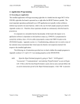
Personal Mechatronics Lab FPGA Interface Board User Manual August 2010 FPGA Interface Board User Manual Table of Contents General Notes ............................................................................................................................................... 3 1 Modular Arrangement of the Board ..................................................................................................... 3 2 Powering the Board .............................................................................................................................. 5 3 Developing Firmware ............................................................................................................................ 6 3.1 Creating FPGA Firmware ............................................................................................................... 6 3.2 Creating PIC18 Firmware .............................................................................................................. 6 4 FPGAConfig Software ............................................................................................................................ 7 5 Board Modes ....................................................................................................................................... 10 5.1 FTDI Programming, User Code Mode ......................................................................................... 10 5.2 PIC Programming Mode .............................................................................................................. 10 5.3 Special Case: Non‐Programmable, User Code Mode .................................................................. 11 5.4 Invalid: Non‐Programmable, No User Code Mode ..................................................................... 11 6 Configuring the FPGA .......................................................................................................................... 11 6.1 FTDI Mode ................................................................................................................................... 11 6.2 PIC Mode ..................................................................................................................................... 12 6.3 Other Configuration Modes ........................................................................................................ 12 6.4 Troubleshooting .......................................................................................................................... 12 7 Sending Signals .................................................................................................................................... 13 7.1 Default FPGA Firmware ............................................................................................................... 13 7.2 Advanced FPGA Firmware ........................................................................................................... 14 7.3 FPGA Pin Assignments ................................................................................................................ 14 Personal Mechatronics Lab 2 FPGA Interface Board User Manual General Notes The FPGA Interface Board is an educational tool that allows a user to create and modify multiple digital connections without the use of physical wires. With this board, users gain first‐hand experience with FPGA chips and are exposed to the chips’ functions and configuration techniques. The board enables users to quickly connect different logic signal inputs and outputs from external devices or boards and achieve integration for the purpose of design verification and prototyping in the early stages of the design process. The FPGA used on this board is the Xilinx Spartan‐3E XC3S250E‐4TQG144C. The board’s main function is to give users the freedom to configure an FPGA to interface and connect signals from different terminals and headers. The user can write a configuration bit file to the board’s serial flash memory either through an FTDI chip or a PIC18 microcontroller. Once the FPGA is powered on or reset, it will read the serial flash and configure itself as required. 1 Modular Arrangement of the Board 1 2 3 4 5c 5b 5a Personal Mechatronics Lab 3 FPGA Interface Board User Manual 6 Module 1 – Power 2 – Programmer 3 – FPGA 4 – DIP Switches 5 – Interface 5a – DevBugger Board 5b – Utility Board 5c – Driver Board 6 – Voltage Translation Personal Mechatronics Lab Description Provides the necessary power for the controller side of the board. It has a 2.1 mm jack for a 12 V adapter, voltage converters, USB socket and the PWR and FPGA LEDs. Contains all necessary components to program the FPGA’s external M25PE20 flash memory. This module includes an FTDI chip with its external EEPROM, a PIC18F2550, PIC mode switches, programming mode switch, and the FTDI and PIC LEDs The main FPGA module with the Spartan‐3E, external flash memory, female headers for connection to the Translator Board, a jumper to disable the FPGA, and parallel cable and JTAG headers. This module contains the two 12‐position DIP switches for configuring inputs to the FPGA. This module contains all of the parts which allow the FPGA Interface Board to connect to the other boards. The interface to the DevBugger Board is provided through 20x2 and 5x2 box headers for connection through ribbon cables. The interface to the Utility Board is provided through a single 5‐ position wire push terminal. The interface to the Driver Board is provided through a number of 2, 3, 4 and 5‐position wire push terminals. One per motor. This module consists of the removable stack board named the Translator Board. It is responsible for bi‐directionally translating external 5V signals to the 3.3V I/O standard used by the FPGA. 4 FPGA Interface Board User Manual 2 Powering the Board The FPGA Interface Board can be powered through the Power module in two different ways. • Power Adaptor: The board can be powered using the 12 V power adaptor located in the top left corner of the Power module. The voltage is regulated down to 5V, 3.3V, 2.5V, and 1.2V using four different regulators. The 5V line is required mostly for the PIC18 and its surrounding components. The 3.3V line is used throughout the board. The 2.5V and 1.2V lines are used by the FPGA alone. • Powering through USB: The board can also be powered using a USB connection alone. The USB socket is positioned in the top right corner of the Power module. In this case the supplied voltage is 5V from the PC and is regulated down to 3.3V, 2.5V and 1.2V. The board can be powered by both the adaptor and USB at the same time. Once the board is turned on, the PWR LED will light up. The obvious advantage of using the USB connection to a PC is the ability to configure the FPGA as well as program the PIC18. However, when a PC is not available, the 12V power adaptor socket provides the advantage of portable board use. If a power‐to‐USB adaptor is available, it can also be used with a USB cable to power the board. Note: When the board is not connected to a PC through USB, the only way to configure the FPGA is through the Parallel Cable Header or JTAG Header. The only way to program the PIC18 is through another board such as the DevBugger board. Fig 1. The Power module of the FPGA Interface board includes a 12 V adaptor socket, four voltage regulators, a USB socket, a bridge rectifier, power switch, two LEDs and a number of capacitors. Personal Mechatronics Lab 5 FPGA Interface Board User Manual 3 Developing Firmware The FPGA Interface Board is very dynamic as it allows the user to completely reconfigure the firmware on both the FPGA and the PIC18. Given the right tools, the user has the ability to design exactly the interface board that their project requires. 3.1 Creating FPGA Firmware In order to develop firmware for the board’s FPGA chip, the user must be familiar with Xilinx ISE Design Suite software. This software is available free from www.xilinx.com through the creation of an account. Xilinx ISE Design Suite comes with a number of tools which are vital to creating a configuration for Xilinx FPGAs. Xilinx’ website provides a number of tutorials and resources which are useful for becoming familiar with FPGAs and Xilinx ISE. Experiment #1 in the laboratory exercises also provides a detailed description of a number of these tools as well as the necessary steps to create a basic FPGA firmware. The Project Navigator is the main tool used. Here, the user can organize their modules and constraint files. Modules can be coded in a number of HDL languages or created through a schematic. The ISim tool allows the user to simulate their design and observe their modular outputs as they depend on different input combinations. The PlanAhead tool allows the user to sort out the physical location of their top module signals on the actual FPGA chip. It can also be used to designate IO standards such as voltage levels for the FPGA pins. The final FPGA configuration can be created in the Project Navigator through the Generate Programming File function. The file is called “bitstream” and is designated with a “.bit” extension. This is the file which can be loaded onto an FPGA’s external serial flash memory and read by the FPGA. 3.2 Creating PIC18 Firmware In order to develop firmware for the board’s PIC18F2550, the user must be familiar with Microchip MPLAB IDE software. This software is available free from www.microchip.com. Along with the official website, there are a large number of great online resources and communities which focus on microcontrollers and microcontroller‐related projects. The DevBugger Board in particular is developed to introduce the most basic users to the power of microcontrollers. Firmware for the FPGA Interface Board’s PIC18 can be developed within MPLAB IDE and comes in the form of a HEX file. It can be programmed to the PIC through the board’s Bootloader feature (section 7.2) or an external board such as the DevBugger Board. In the case of using an external board, the PIC18 must be removed from the FPGA Interface Board and then once again placed back inside the Programmer module. Personal Mechatronics Lab 6 FPGA Interface Board User Manual 4 FPGAConfig Software The FPGA Interface Board’s accompanying software, named FPGAConfig, allows the user to transfer both FPGA and PIC18 firmware to their respective chips on the board. From top to bottom, the software is divided into four modules – Connection Status, FPGA Configuration, PIC18 Firmware Modification, and Function Status. Fig 2. The FPGAConfig software application allows users to connect to the FPGA Interface Board, program, verify, and read bitstream files to/from the flash memory, append PIC18 user code and launch Microchip PDFSUSB to program the PIC18. Connection Status Module Connect to Device This function lets the user to connect to the FPGA Interface Board and recognize the mode that the board is currently in – either FTDI or PIC. FPGAConfig must recognize a connection before being able to perform any operations within the FPGA Configuration module. Personal Mechatronics Lab 7 FPGA Interface Board User Manual FPGA Configuration Module Open Bitstream … This function allows the user to select a file from their PC with a “.bit” extension. This file becomes the reference file for programming to the board and verifying the current board configuration. Program Bit File to FPGA This function will transfer the FPGA configuration held within the selected bitstream to the FPGA’s external serial flash memory. The data will be transferred either through the FTDI chip (in FTDI configuration mode) or the PIC18 (in PIC configuration mode). After programming the memory, this function will restart the FPGA, forcing the chip to read the new configuration from the memory chip. Verify Program This function will read the flash memory’s current contents and compare them against the selected bitstream file in order to confirm that the FPGA will configure itself to the exact file of the user’s choice. After verification, the FPGA is restarted. Erase Configuration This function will erase all data from the FPGA’s external flash memory. Restarting the FPGA or powering on the board when the flash memory is empty will not place any configuration onto the FPGA. Verify Blank This function will read the flash memory’s current contents and compare them against a blank configuration. Read Configuration and Save to File This function will read the flash memory’s current contents and then save them in a “.bit” extension file in the location of the user’s choice. The newly‐created file can be reprogrammed back onto the flash memory in order to restore the FPGA’s previous function. PIC18 Firmware Modification Module Open User Hex … This function allows the user to select a file from their PC with a “.hex” extension. This file should be a user code hex file which was exported from MPLAB IDE. It’s important that the user code has an origin of 0x2500 or else the Append Hex File to FPGA Programming Firmware function will fail. For more information please see section 7. Append Hex File to Default PIC18 Firmware This function copies the code out of the selected user hex file starting from 0x2500 until the first empty line and adds it to the default PIC18 firmware file located in the FPGAConfig main software folder under Bootloader App/PICFPGA.hex. Once the two files are merged, the resulting file can be saved in the location of the user’s choice. If an “Invalid User Hex” message is encountered, this means that the exported user code hex file ends before the address 0x2500 is encountered. It is vital that the user hex file has an origin of 0x2500. Personal Mechatronics Lab 8 FPGA Interface Board User Manual Download Firmware to PIC18 This function launches Microchip’s PDFSUSB application which enables the user to select a hex file and program it to a connected PIC18. Once the user hex file has been combined with the default firmware, this application can be used to select the newly‐created firmware and program it onto the PIC18. It’s important that the user first puts the PIC18 into Bootloader mode. This can be done by holding the push button switch below the external IO pins while the board is powered on, or while the PIC is being reset. After PDFSUSB programs the PIC18, either the PIC or the entire FPGA Interface Board must be reset in order for the new firmware to take effect. Fig 3. Microchip’s PDFSUSB application can be launched from FPGAConfig to detect the PIC18 in Bootloader mode and program it with a hex file of the user’s choice. Once the user code has been merged with the default PIC18 firmware through the append function, this application can be used to transfer the combined hex file to the PIC18. Note: The instructions above the Download Firmware button in FPGAConfig must be followed in order for PDFUSB to detect the PIC in Bootloader mode. If the PIC is correctly placed in Bootloader mode, PDFUSB’s drop down menu should find the device and the final HEX can be loaded with the Load HEX File button and downloaded with the Program Device button. Personal Mechatronics Lab 9 FPGA Interface Board User Manual Note: Problems detecting the device in PDFSUSB were observed on Windows Vista and Windows 7. These stemmed from the PC’s ability to turn off USB devices that it felt were being unused at the moment. To fix this issue: Connect the FPGA Interface Board to the PC and navigate to the devices menu. Right‐click and select “Properties” on the FPGA board. In the Hardware tab, click on “Properties” and then on “Change Settings”. Under “Power Management”, uncheck “Allow the computer to turn off this device to save power” and click OK. A reconnection of the board may be necessary. Running PDFSUSB.exe externally (from the Start Menu or folder) as Administrator may also be required. Function Status Module This module contains a configuration status label which tells the user when FPGAConfig has finished a certain process. The configuration status label also displays certain error messages when the program is unable to complete a process. Error messages are also often displayed in pop‐up windows. This module also displays a progress bar to let the user know of any function’s progress. Note that during an Erase Configuration command (a relatively quick process), the progress bar moves particularly fast and may be missed, in this case check the status label for “Device Erased”. 5 Board Modes The FPGA Interface Board currently has two main modes which it can be put into. These are selected by the two slide switches in the Programming module of the board. It’s important to understand the two modes to successfully configure and enable the FPGA as required. 5.1 FTDI Programming, User Code Mode This mode is the primary mode the user should be in when using the FPGA Interface Board. It is selected by having both switches in the DOWN position. The large switch signifies that the FPGA will be programmed in FTDI mode while the smaller one shows that the FPGA will be enabled and that the PIC18 will not attempt to program the FPGA itself but will instead execute its user code. If no user code has been appended to the PIC18 firmware, the PIC will do nothing. 5.2 PIC Programming Mode This mode is selected by having both switches in the UP position. The larger switch signifies that the PIC, not FTDI, will attempt to program the FPGA while the smaller one shows that instead of running its user code, the PIC will be in its “FPGA‐programming” mode. The FTDI is held in reset. Once the bitstream has been programmed, the PIC will reset the FPGA. However the PIC still controls signals on the SPI bus and may conflict with FPGA operation. The PIC/FPGA ENABLE Mode is designed to avoid this problem and is described below. Personal Mechatronics Lab 10 FPGA Interface Board User Manual 5.3 Special Case: NonProgrammable, User Code Mode This mode is selected by having the larger switch in the UP position, signifying the PIC’s control over the flash memory, and the smaller switch in the DOWN position, showing that the PIC enables the FPGA and continues on to run user code. Although recognized by FPGAConfig in PIC mode, the board cannot program the FPGA in neither PIC nor FTDI mode while the switches are in this position. Functionally, this mode should only be entered to enable the FPGA after it has been programmed in PIC/PIC PROG mode. 5.4 Invalid: NonProgrammable, No User Code Mode This mode is selected by having the larger switch in the DOWN position, signifying the FTDI’s attempt to program the flash memory, and the smaller switch in the UP position, showing that the PIC is also attempting to program the flash memory. Although starting the board in this mode will enable the FPGA, this mode will not be able to program the FPGA nor run user code from the PIC18. As such, the user should refrain from entering this mode. 6 Configuring the FPGA The FPGA Interface Board allows the user to program a configuration onto the FPGA in a number of different ways. These include the two main FTDI and PIC modes, as well as additional access to the FPGA programming pins through female headers. 6.1 FTDI Mode The FTDI programming mode is significantly faster and more reliable that the PIC programming mode. At the same time, this mode has the PIC running user code with no conflicts on the serial bus controlling the FPGA. As such, the user is advised to remain in this mode whenever possible. With this mode, the bitstream is first transferred through USB from the PC to the FTDI FT2232D chip. The data is then sent from the FTDI chip to the M25PE20 flash memory. When programming in FTDI mode, it’s important to make sure that the board is in FTDI/FPGA ENABLE mode. This can be done by having both switches in the programming module in the DOWN position as in Section 5.1. Because programming in FTDI mode also requires the board to be in FPGA ENABLE mode, there is no need for any additional input from the user once the bitstream is programmed and the FPGA will automatically reset as the PIC runs user code. Personal Mechatronics Lab 11 FPGA Interface Board User Manual 6.2 PIC Mode The PIC programming mode is both slower and slightly less reliable that the FTDI programming mode. In this mode, the PIC18 uses its FPGA‐programming firmware (available as the default PICFPGA.hex) to program the FPGA’s flash memory. With this mode, the bitstream is sent through the USB from the PC to the PIC18 in smaller packets than the FTDI transfer. The data is then written to the serial memory chip by the PIC18. When programming in PIC mode, it’s important that the board is in PIC/PIC PROG mode as shown in Section 5.2. Once the PIC finishes programming the memory, the FPGA is reset. However the FPGA may fail to correctly read from the flash memory because the PIC18 still has control over some of the signals. As a result, it’s important that the user switches to PIC/FPGA ENABLE mode (Section 5.3) to successfully enable the FPGA. 6.3 Other Configuration Modes Apart from allowing the user to program the FPGA through the PIC and FTDI modes, the FPGA Interface Board also provides two female headers which can be used to configure the FPGA. Parallel Cable Header The parallel cable header gives the user direct access to the SPI bus through which the FTDI and PIC program the serial memory. This is a master slave bus when the FTDI, PIC, and FPGA are all masters, while the M25PE20 memory is a slave. Advanced users may be able to connect other devices as masters to the bus. This header may also be used for debugging a particular board by attaching another FPGA Interface Board nearby, connecting the two SPI buses through the parallel cable headers, and disabling the FPGA on the working board through the jumper. If the FPGA on the faulty board is still functional, it should configure itself from the functional board’s memory. JTAG Header The JTAG (Joint Test Action Group) header provides a way for advanced users to program the FPGA without using the SPI master slave bus. Using this method, which is supported by most FPGA vendors, a configuration can be downloaded directly to the FPGA from the PC. The JTAG signals – TDI, TDO, TMS, TCK – are tied to special JTAG programming pins on the FPGA – 144, 109, 108, 110 respectively. For more information, see the “Spartan‐3 Generation Configuration User Guide” from Xilinx. 6.4 Troubleshooting If the user experiences difficulty – either through inability to program the memory chip or the FPGA’s inability to configure from the memory – the following procedure should be followed: ‐ Close all existing sessions of FPGAConfig ‐ Turn the board off, place it in FTDI/FPGA ENABLE mode and power on ‐ Open a new session of FPGAConfig and connect to the board ‐ Erase the current configuration and verify that it is blank Personal Mechatronics Lab 12 FPGA Interface Board User Manual 7 Sending Signals Once the board has been successfully configured with a bitstream, signals can be sent to and from the FPGA through the 5x2 box header, 20x2 box header, 24 DIP switches, and wire push terminals. The following two subsections will explain the FPGA Interface Board’s provided default and advanced firmware configurations. Section 7.3 provides advanced users with a table which can be used to place terminal, header, and switch signals at the correct FPGA pin numbers. 7.1 Default FPGA Firmware The default FPGA firmware is the FPGA configuration that is already on the FPGA Interface Board at the very beginning. In case the board is reprogrammed, the default firmware can always be found in the FPGA Interface Board\Firmware folder. The purpose of this firmware is to provide the user with as many different routing combinations as possible from the 20x2 box header (which connects to the DevBugger Board) to the wire push terminals (which connect to the Driver Board and Utility Board). The user can send signals to the FPGA from the 24 DIP switches and adjust its configuration as required to best match their intended connections. By default, the Utility Board terminals are tied to PORTE on the 40‐pin header. The utility signals – SQR, CHA, CHB – correspond to RE0, RE, RE1 respectively. CHA and CHB are DevBugger outputs, while SQR is an output. The bottom‐most DIP switch must be HIGH to enable the Utility signals. The Driver Board connects to the remaining DevBugger signals as follows: ‐ Each motor has two DIP switches which select the PORT from which the motor receives its signals. For example keeping the two BIP switches 00 means the bipolar motor is controlled by PORTA. 01 corresponds to PORTB, 10 to PORTC and 11 to PORTD. ‐ Each PORT has three DIP switches to select which of its pins is designates as ‘first’. For example, setting the three PORTB pins to 000 means that any motor connected to PORTB will receive RB0 at the top‐most terminal. Setting the switches to 010 means that any motor connected to PORTB will instead receive RB2 as the top‐most terminal signal. ‐ For further understanding, consider that with all of the DIP switches set to 0, RA0 will control the Unipolar CLK, the DC Motors DC1‐DIR, the Bipolar CLK, the Brushless ON/OFF, and the Servo CLK. This type of firmware gives the user a lot of freedom when connecting signals. As an interfacing example, consider the need to connect the signals RC3:6 to the DC Motor terminals. The following steps would need to be taken: ‐ Set the DCs two DIP switches to 10 to select PORTC ‐ Set the PORTC switches to 011 to select RC3 as the first pin The connections are now established as required. Personal Mechatronics Lab 13 FPGA Interface Board User Manual 7.2 Advanced FPGA Firmware Similar to the default firmware, the advanced firmware tries to give the user as much freedom as possible while also adding the connections from the 5x2 box header. In this case, the header would be connected to the external I/O pins of the PIC18 on the DevBugger Board. By adjusting the two bottom‐ most switches, the user has the ability to configure the FPGA on‐the‐go and connect different PIC18 signals to different motors and/or the utility board. The following table should be used when adjusting these two switches. Connecting any terminals to the 5x2 box header will disable the connection between that terminal and the 20x2 header. Switch 11 0 DC Motors B3 – DC1 DIR B4 – DC1 CLK B6 – DC2 DIR B7 – DC2 CLK 1 Brushless + Servo B3 – ON/OFF B4 – FWD/REV B6 – CLK B7 ‐ none Switch 12 0 1 Bipolar Stepper Utility Board A4 – CLK A4 – SQR C2 – SS C2 – CHA C6 – DIR C6 – CHB 7.3 FPGA Pin Assignments DIP Switch FPGA Pin # 10‐Pin Header FPGA Pin # top 1 57 Ground ‐ top 2 69 VCC ‐ top 3 78 RE3 ‐ top 4 84 RB4 94 top 5 89 RB6 96 top 6 95 RB3 97 top 7 101 RB7 103 top 8 107 RC6 104 top 9 111 RC2 105 top 10 114 RA4 112 top 11 119 Utility Terminal FPGA Pin # top 12 120 Square 43 bottom 1 129 Ground ‐ bottom 2 136 Channel A 50 bottom 3 141 Ground ‐ bottom 4 10 Channel B 51 bottom 5 12 Servo Terminal FPGA Pin # bottom 6 18 Clock 52 bottom 7 29 Ground ‐ bottom 8 36 Bipolar Terminal FPGA Pin # bottom 9 38 Clock 143 bottom 10 41 Start/Stop 68 bottom 11 47 Direction 66 bottom 12 48 Ground ‐ Personal Mechatronics Lab 14 FPGA Interface Board User Manual 40‐Pin Header FPGA Pin # DC Terminal FPGA Pin # Ground ‐ DC1 Direction 31 VCC ‐ DC1 Clock 77 KPD ‐ DC2 Direction 76 RA0 4 DC2 Clock 75 RA1 3 Ground ‐ RA2 2 Unipolar Terminal FPGA Pin # RA3 142 Clock 74 RA4 140 S0 59 RA5 139 S1 58 RA6 135 Ground ‐ RA7 134 Brushless Terminal FPGA Pin # RB0 35 On/Off 54 RB1 34 Fwd/Rev 53 RB2 33 Ground ‐ RB3 32 RB4 26 RB5 25 RB6 23 RB7 21 RC0 126 RC1 125 RC2 124 RC3 123 RC4 122 RC5 117 RC6 116 RC7 113 RD0 20 RD1 17 RD2 16 RD3 15 RD4 14 RD5 8 RD6 7 RD7 5 RE0 132 RE1 131 RE2 130 Personal Mechatronics Lab 15