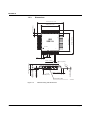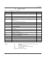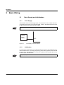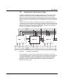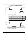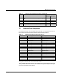
1
AUTOMATIONWORX
User Manual
UM EN IBS SRE 1A
Order No.: 2888741
INTERBUS Register Expansion Chip
IBS SRE 1A
AUTOMATIONWORX
User Manual
INTERBUS Register Expansion Chip IBS SRE 1A
06/2006
Designation:
UM EN IBS SRE 1A
Revision:
01
Order No.:
2888741
This user manual is valid for:
Designation
Order No.
IBS SRE 1A
2746595
7295_en_01
PHOENIX CONTACT
IBS SRE 1A
Please Observe the Following Notes
In order to ensure the safe use of the product described, we recommend that you read this
manual carefully. The following notes provide information on how to use this manual.
User Group of This Manual
The use of products described in this manual is oriented exclusively to qualified electricians
or persons instructed by them, who are familiar with applicable standards and other
regulations regarding electrical engineering and, in particular, the relevant safety concepts.
Phoenix Contact accepts no liability for erroneous handling or damage to products from
Phoenix Contact or third-party products resulting from disregard of information contained
in this manual.
Explanation of Symbols Used
The attention symbol refers to an operating procedure which, if not carefully followed, could
result in damage to hardware and software or personal injury.
The note symbol informs you of conditions that must strictly be observed to achieve
error-free operation. It also gives you tips and advice on the efficient use of hardware and
on software optimization to save you extra work.
The text symbol refers to detailed sources of information (manuals, data sheets, literature,
etc.) on the subject matter, product, etc. This text also provides helpful information for the
orientation in the manual.
We Are Interested in Your Opinion
We are constantly striving to improve the quality of our manuals.
Should you have any suggestions or recommendations for improvement of the contents
and layout of our manuals, please send us your comments.
PHOENIX CONTACT GmbH & Co. KG
Documentation Services
32823 Blomberg
Germany
Phone
Fax
E-mail
PHOENIX CONTACT
+49 - 52 35 - 30 0
+49 - 52 35 - 34 20 21
[email protected]
7295_en_01
IBS SRE 1A
General Terms and Conditions of Use for Technical Documentation
Phoenix Contact GmbH & Co. KG reserves the right to alter, correct, and/or improve the
technical documentation and the products described in the technical documentation at its
own discretion and without giving any notice.
The provision of technical documentation (in particular data sheets, installation
instructions, manuals, etc.) does not constitute any further duty on the part of
Phoenix Contact GmbH & Co. KG to furnish information on alterations to products and/or
technical documentation. Any other agreement shall only apply if expressly confirmed in
writing by Phoenix Contact GmbH & Co. KG. Please note that the supplied documentation
is product-specific documentation only.
Although Phoenix Contact GmbH & Co. KG makes every effort to ensure that the
information content is accurate, up-to-date, and state-of-the-art, technical inaccuracies
and/or printing errors in the information cannot be ruled out.
Phoenix Contact GmbH & Co. KG does not offer any guarantees as to the reliability,
accuracy or completeness of the information provided. Phoenix Contact GmbH & Co. KG
accepts no liability or responsibility for errors or omissions in the content of the technical
documentation (in particular data sheets, installation instructions, manuals, etc.).
As far as is permissible by applicable jurisdiction, no guarantee or claim for liability for
defects whatsoever shall be granted in conjunction with the information available in the
technical documentation, whether expressly mentioned or implied. This information does
not include any guarantees on quality, does not describe any fair marketable quality and
does not make any claims as to quality guarantees or guarantees on the suitability for a
special purpose.
Phoenix Contact GmbH & Co. KG reserves the right to alter, correct, and/or improve the
information and the products described in the information at its own discretion and without
giving any notice.
7295_en_01
PHOENIX CONTACT
IBS SRE 1A
Statement of Legal Authority
This manual, including all illustrations contained herein, is copyright protected. Use of this
manual by any third party is forbidden. Reproduction, translation, or electronic and
photographic archiving or alteration requires the express written consent
of Phoenix Contact. Violators are liable for damages.
Phoenix Contact reserves the right to make any technical changes that serve the purpose
of technical progress.
Phoenix Contact reserves all rights in the case of patent award or listing of a registered
design. Third-party products are always named without reference to patent rights. The
existence of such rights shall not be excluded.
Internet
Up-to-date information on Phoenix Contact products can be found on the Internet at:
www.phoenixcontact.com
Make sure you always use the latest documentation.
It can be downloaded at:
www.download.phoenixcontact.com
A conversion table is available on the Internet at:
www.download.phoenixcontact.com/general/7000_en_00.pdf
PHOENIX CONTACT
7295_en_01
Table of Contents
1
2
3
4
Introduction ................................................................................................................................ 1
1.1
Serial Register Expansion Chip ............................................................................ 1
1.2
Area of Application ................................................................................................ 1
1.3
Housing Type ........................................................................................................ 2
1.3.1
Pin Assignment ...................................................................................... 2
1.3.2
Pin Table ............................................................................................... 3
1.3.3
Dimensions ............................................................................................ 4
1.3.4
Signal Description .................................................................................. 5
Basic Wiring ...............................................................................................................................6
2.1
Clock Supply and Initialization .............................................................................. 6
2.1.1
Clock Supply .......................................................................................... 6
2.1.2
Initialization ............................................................................................ 6
2.2
Connection to the Protocol Chips.......................................................................... 7
2.2.1
Serial Interface Timing ........................................................................... 8
2.3
Setting the Data Length ...................................................................................... 10
Microprocessor Access ...........................................................................................................11
3.1
Timing for the Microprocessor Interface ............................................................. 12
3.2
Address Area Assignment................................................................................... 13
3.2.1
INTERBUS Data Registers .................................................................. 14
3.2.2
Configuration Register ......................................................................... 14
3.3
Interrupt Operation .............................................................................................. 16
Technical Data and Ordering Data ..........................................................................................17
7295_en_01
4.1
Technical Data .................................................................................................... 17
4.2
Ordering Data...................................................................................................... 17
PHOENIX CONTACT
i
IBS SRE 1A
ii
PHOENIX CONTACT
7295_en_01
Introduction
1
Introduction
This manual describes the IBS SRE 1A register expansion chip for the INTERBUS SUPI
protocol chip family. It can be used to easily expand the data length of the protocol chips if
the internal data registers are insufficient. The maximum of six additional data words can
be accessed via a microprocessor.
This manual and the manuals for INTERBUS SUPI protocol chips can be used to
implement custom INTERBUS devices, which should be subjected to a conformance test.
INTERBUS is a serial sensor/actuator bus. It comprises a central intelligent controller
board (controller or IB master) in a host system and distributed I/O modules.
IBS SUPI protocol chips are used for integrating I/O modules in an INTERBUS network. In
this document, "IBS SUPI" refers to all INTERBUS protocol chips in the SUPI range.
On the I/O side, the IBS SUPI has a multi-function interface (MFP Multi-Function Pins).
Depending on the function of the INTERBUS device, the MFP interface can be configured
as a direct I/O interface or as a processor interface.
Electrostatic discharge
The chip can be damaged or destroyed by electrostatic discharge. When handling the
chip, observe the necessary safety precautions against electrostatic discharge (ESD)
according to EN 61340-5-1 and EN 61340-5-2.
1.1
Serial Register Expansion Chip
The Serial Register Expansion chip (SRE) is an ASIC in 0.8-µm gate array technology with
approximately 4000 gate equivalents. It has one serial input and one serial output as well
as a microprocessor interface for accessing the internal INTERBUS data registers. The
IBS SRE 1A was specially developed as a register expansion for IBS SUPI INTERBUS
protocol chips. However, it can also be used in other applications.
For the ordering data, please refer to "Technical Data and Ordering Data" on page 1-17.
1.2
Area of Application
The IBS SRE 1A is suitable for use in industrial applications.
Table 1-1
Area of application
Value
Amount
Minimum
7295_en_01
Typical
Maximum
Supply voltage
4.5 V
5.0 V
5.5 V
Temperature
-40°C
+25°C
+85°C
PHOENIX CONTACT
1
IBS SRE 1A
1.3
Housing Type
The IBS SRE 1A is housed in a QFP44 housing.
1.3.1
Pin Assignment
2 5
G N D
3 5
S D I
2 0
/C lK R O
/IR Q
V C C
4 0
A 2
V C C
G N D
L a O u D
1 5
/L a In D
/R D
G N D
/W R
D 7
D 6
D 5
D 4
G N D
1 0
G N D
V C C
D 3
D 2
D 0
PHOENIX CONTACT
5
D 1
1
2
A 1
A 0
/R e s R e g
Figure 1-1
/C lk R I
A 3
IB S
S R E 1 A
re s e rv e d
G N D
V C C
/E N D R R
/E N D R W
/E N C R
G N D
G N D
V C C
3 0
O S C
S D O
/R e s U
K 0
K 1
K 2
(Quad Flat Pack)
7 2 9 5 A 0 0 1
QFP44 housing with pin assignment
7295_en_01
Introduction
1.3.2
Table 1-2
7295_en_01
Pin Table
QFP44 pin table
Pin No.
Pin Name
Pin No.
Pin Name
1
D0
23
VCC
2
D1
24
/ENDRR
3
D2
25
/ENDRW
4
D3
26
/ENCR
5
VCC
27
GND
6
GND
28
GND
7
GND
29
VCC
8
D4
30
/ResU
9
D5
31
K0
10
D6
32
K1
11
D7
33
K2
12
/WR
34
OSC
13
/RD
35
SDO
14
A0
36
/ClkRO
15
A1
37
/IRQ
16
GND
38
Test
17
VCC
39
VCC
18
A2
40
GND
19
A3
41
LaOuD
20
/ClkRI
42
/LaInD
21
SDI
43
/ResReg
22
GND
44
GND
PHOENIX CONTACT
3
IBS SRE 1A
1.3.3
Dimensions
1 3 .9 m m ( 0 .5 4 7 in .) + /- 0 .2 5
1 m m
( 0 .0 3 9 in .)
1 0 m m ( 0 .3 9 4 in .) + /- 0 .1
3 0
2 5
3 5
1 3 .9 m m
1 0 m m
4 0
( 0 .3 9 in .)
IB S
S R E 1 A
( 0 .5 4 7 in .)
2 0
1 5
In d e x -M a rk e
1
5
0 .8 m m
1 0
( 0 .0 3 1 in .)
1 m m
( 0 .0 3 9 in .)
0 .2 m m ... 0 .4 5 m m
0 .2 m m ( 0 .0 0 8 in .)
( 0 .0 0 8 in . ... 0 .0 1 8 in .)
( 0 .0 0 6 in .)
0 .6 5 m m ... 1 .0 3 m m
0 .1 m m
( 0 .0 0 4 in .)
( 0 .0 2 6 in . ... 0 .0 4 1 in .)
S E A T IN G
0 .1 5 m m
0 .0 5 m m ... 0 .5 m m
( 0 .0 0 2 in . ... 0 .0 2 in .)
1 .9 m m ... 2 .2 m m
( 0 .0 7 5 in . ... 0 .0 8 7 in .)
m a x . 2 .4 5 m m
( 0 .0 9 7 in .)
m a
x .
1 0
°
P L A N E
7 2 9 5 A 0 0 2
Figure 1-2
4
PHOENIX CONTACT
QFP44 housing with dimensions
7295_en_01
Introduction
1.3.4
Table 1-3
Signal Description
Signal description for the IBS SRE 1A
Designation
Meaning
Type
OSC
Oscillator input
ST
K0
K1
K2
Configuration inputs for the internal registers
ST
D0 - D7
Data bus for the microprocessor interface
BD
A0 - A3
Address bus for the microprocessor interface
CI
/RD
/WR
/IRQ
/Read
/Write
/Interrupt Request
CI
CI
B2
/ENCR
Enable signal for the configuration register1
CI
1
CI
Control bus for the microprocessor interface
/ENDRR
/READ enable signal for the data registers
1
/ENDRW
/WRITE enable signal for the data registers
CI
SDI
Data input for the IBS SRE 1A (should be connected to data output ToExR1 or
ToExR2 of the IBS SUPI)
ST
SDO
Data output for the IBS SRE 1A (should be connected to data input FromExR of
the IBS SUPI)
B2
/ClkRI
Clock input for the internal shift registers for SRE 1A
CI
/ClkRO
Clock output for the internal shift registers for other IBS SRE 1A chips or
conventional shift registers
B2
LaOuD
Transmission signal for output data for the IBS SRE 1A
INTERBUS → OUT memory area
ST
/LaInD
Transmission signal for input data for the IBS SRE 1A
IN memory area → INTERBUS
ST
/ResReg
Reset signal for the internal data registers of the IBS SRE 1A
ST
/ResU
Initialization reset
STpu
Test
Leave open; test pin for in-circuit test by the ASIC manufacturer
B2
VCC
Supply voltage +5 V
GND
Ground
1
In normal microprocessor mode, these signals should be grouped as the chip select for the IBS SRE 1A.
Cell types:
BD:
CI:
ST:
STpu:
B2:
Bidirectional, with Schmitt trigger inputs and 2 mA driver outputs
CMOS input
CMOS Schmitt trigger input
CMOS Schmitt trigger input with internal pull-up
2 mA driver output
Electrical data: See section 4 on page 17
7295_en_01
PHOENIX CONTACT
5
IBS SRE 1A
2
Basic Wiring
2.1
2.1.1
Clock Supply and Initialization
Clock Supply
The IBS SRE 1A has a Schmitt trigger input. The required clock can be either that of the
connected microprocessor or that of the IBS SUPI. However, if the IBS SUPI clock is used,
the IBS SUPI must be clocked using an oscillator.
The quartz circuit of the IBS SUPI must not be modified.
1 6 M H z
q u a rtz
o s c illa to r
O S C
5 1 0 4 B 0 0 3
Figure 2-1
2.1.2
Clock supply for the IBS SRE 1A
Initialization
In order to place the IBS SRE 1A in a defined state after power up, the initialization input
/ResU should be set to "Low" during the power up phase. During operation, /ResU should
be set to "High". The simplest option is to connect the /ResU input of the IBS SRE 1A with
the /ResU input of the IBS SUPI.
The power up phase must be at least 125 ns.
6
PHOENIX CONTACT
7295_en_01
Basic Wiring
2.2
Connection to the Protocol Chips
In addition to the serial data inputs and outputs, the IBS SRE 1A has a microprocessor
interface for parallel access to internal INTERBUS data registers. Connection to the
IBS SUPI is via the serial data inputs and outputs and the associated control signals
(Latch, Clock, Reset). Since the IBS SRE 1A was developed as an expansion chip for the
IBS SUPI, the inputs and outputs for data and control signals can be connected together
directly.
The IBS SRE 1A is connected to the IBS SUPI according to the specifications for the
connection of a register expansion in the IBS SUPI user manual. The serial data input SDI
of the IBS SRE 1A is connected to the shift register data output ToExR1 or ToExR2 of the
IBS SUPI. The serial data output SDO of the IBS SRE 1A should be connected to pin
FromExR of the IBS SUPI. This closes the data ring.
F ro m E x R
/L a In D
L a O u D
/R e s R rg
S U P I
C lk E x R
C lk R I
T o E x R 1
o d e r
T o E x R 2
S D I
C lk R O
S R E 1 A
S D O
K 0 ,K 1 ,K 2
D 0 -D 7
A 0 -A 3
/C S /W R /R D /IR Q
D 0 -D 7
C lk R I
S D I
C lk R O
S R E 1 A
S D O
K 0 ,K 1 ,K 2
A 0 -A 3
/C S /W R /R D
D 0 -D 7
A 0 -A 3
/C S /W R /R D /IR Q
D A T A
A D D R E S S
C O N T R O L
5 1 0 4 B 0 0 4
Figure 2-2
Connection to the IBS SUPI
It is also possible to connect up to six expansion chips in succession or to use other
conventional shift registers. The signals LaOuD, /LaInD, and /ResReg should be assigned
in parallel to all IBS SRE 1A chips. The /ClkExR clock output of the SUPI should be
connected to the ClkRI clock input of the IBS SRE 1A. For the clock supply of other
IBS SRE 1A chips or conventional shift registers, the /ClkRO clock output of the
IBS SRE 1A should be used.
7295_en_01
PHOENIX CONTACT
7
IBS SRE 1A
2.2.1
Serial Interface Timing
The timing for the serial interface matches the timing for the IBS SUPI register expansion.
The timing for the serial interface of the IBS SRE 1A can be found in the diagrams below.
/C lk R I
t1
S D I
n
n + 1
t2
Figure 2-3
8
PHOENIX CONTACT
5 1 0 4 B 0 0 5
Timing for the serial IN interface of the IBS SRE 1A
Symbol
Explanation
Time
t1
SDI valid after the rising edge of /ClkRI min.
1.1 ns
t2
SDI valid before the rising edge of /ClkRI min.
12 ns
7295_en_01
Basic Wiring
/C lk R I
t2
t1
/C lk R O
t4
t3
S D O
5 1 0 4 B 0 0 6
Figure 2-4
7295_en_01
Timing for the serial OUT interface of the IBS SRE 1A
Symbol
Explanation
Time
t1
Minimum delay /ClkRI after /ClkRO
9.9 ns
t2
Maximum delay /ClkRI after /ClkRO
15.5 ns
t3
SDO valid after the rising edge of /ClkRI min.
16.6 ns
t4
SDO valid after the rising edge of /ClkRO min.
1.1 ns
PHOENIX CONTACT
9
IBS SRE 1A
2.3
Setting the Data Length
The data length of the serial register expansion chip can be set to 0 to 6 words. The data
length of the IBS SRE 1A can be configured via hardware and via software.
For configuration via hardware, the data length is set by wiring the three pins K0, K1, and
K2.
These pins can be used to make the following settings:
Table 2-1
Configuration of the data length
K2
K1
K0
Data Width
0
0
0
0 words
0
0
1
1 word
0
1
0
2 words
0
1
1
3 words
1
0
0
4 words
1
0
1
5 words
1
1
0
6 words
As an option, the data width can be set by writing to the CONF register of the IBS SRE 1A
(addressing, see section 3.2.2 on page 14).
10
PHOENIX CONTACT
7295_en_01
Microprocessor Access
3
Microprocessor Access
The IBS SRE 1A is addressed by a microprocessor such as an I/O component
(e.g., RAM). The IBS SRE 1A has an 8-bit bidirectional data bus (D0 to D7), a 4-bit
address bus (A0 to A3), active-low control signals Chip Select /CS (/ENCR, /ENDRR,
/ENDRW), Read (/RD), and Write (/WR) and an active-low interrupt request line (/IRQ).
The separate enable signals can be used to specifically enable individual data areas of the
IBS SRE 1A.
The meaning of the signals can be found in the following table.
Table 3-1
Meaning of chip select signals
Enable Signal
Meaning
/ENCR
Enable signal for the configuration register
/ENDRR
Enable signal for read access to the data registers
/ENDRW
Enable signal for write access to the data registers
In normal microprocessor mode, these signals should be grouped as the chip select for the
IBS SRE 1A.
S R E 1 A
/E N C R
/C S
/E N D R R
/E N D R W
7 2 9 5 A 0 0 7
Figure 3-1
Chip select signal for the IBS SRE 1A
The timing in Figure 3-2 must be observed exactly. In the event of access problems
when using a Motorola processor (e.g., problems with configuration register access), the
problems can be solved by connecting pin /ENCR to GND.
7295_en_01
PHOENIX CONTACT
11
IBS SRE 1A
3.1
Timing for the Microprocessor Interface
Write access
/C S
A 3 ..0
t1
t2
t5
/W R
t4
t3
V a lid d a ta
D 7 ..0
5 1 0 4 B 0 1 0
Figure 3-2
Timing for write access
Table 3-2
Timing for the microprocessor interface - write access
Symbol
Explanation
Minimum
Time
t1
Addresses and /CS valid before negative edge of /WR
5 ns
t2
Addresses and /CS valid after positive edge of /WR
5 ns
t3
Valid data before positive edge of /WR
15 ns
t4
Valid data after positive edge of /WR
10 ns
t5
/WR pulse width
30 ns
Read access
/C S
A 3 ..0
t6
t1
t7
0
/R D
t9
t8
V a lid d a ta
D 7 ..0
5 1 0 4 B 0 1 1
Figure 3-3
12
PHOENIX CONTACT
Timing for read access
7295_en_01
Microprocessor Access
Table 3-3
Timing for the microprocessor interface - read access
Symbol Explanation
Time
Minimum Maximum
t6
Addresses and /CS stable before negative edge of
/RD
10 ns
t7
Addresses and /CS stable after positive edge of /RD
10 ns
t8
Valid data after negative edge of /RD
25 ns
t9
Data bus high resistance after positive edge of /RD
26 ns
t10
/RD pulse width
3.2
30 ns
Address Area Assignment
Four address lines (A0 - A3) are available for the IBS SRE 1A. The address area that can
be accessed via the microprocessor interface has the following structure:
Table 3-4
Address area assignment for the IBS SRE 1A
Relative Address
Write Register
Read Register
0
IBS IN byte 0
IBS OUT byte 0
1
IBS IN byte 1
IBS OUT byte 1
2
IBS IN byte 2
IBS OUT byte 2
3
IBS IN byte 3
IBS OUT byte 3
4
IBS IN byte 4
IBS OUT byte 4
5
IBS IN byte 5
IBS OUT byte 5
6
IBS IN byte 6
IBS OUT byte 6
7
IBS IN byte 7
IBS OUT byte 7
8
IBS IN byte 8
IBS OUT byte 8
9
IBS IN byte 9
IBS OUT byte 9
10
IBS IN byte 10
IBS OUT byte 10
11
IBS IN byte 11
IBS OUT byte 11
12
CONFREG
CLEAR IRQ
13
Unused
Unused
14
Unused
Unused
15
Unused
Unused
All registers of the IBS SRE 1A have the default value "0".
The INTERBUS data registers are set to their default value via the initialization input /ResU
and by an INTERBUS reset. However, the CONFREG configuration register can only be
reset via the initialization input (/ResU).
7295_en_01
PHOENIX CONTACT
13
IBS SRE 1A
3.2.1
INTERBUS Data Registers
The INTERBUS data registers with addresses 0 to 11 are designed for the exchange of
I/O data between a slave application and the INTERBUS master. The "IB IN byte" data
registers should be written by the slave application. This data is IN data for the INTERBUS
master, whereas the "IB OUT byte" data registers should be read by the slave application.
This data is OUT data for the INTERBUS master.
The value of the data registers falls as the address rises, i.e., for a device with a data width
of 8 bytes, the byte with address 0 is the high byte and the byte with address 7 is the low
byte.
The value of the data in the memory areas of the IBS SUPI and any other register
expansion chips is shown below:
High byte
Low byte
3.2.2
High byte of the IBS SUPI
.
Memory area of the IBS SUPI
.
Low byte of the IBS SUPI
.
High byte of the first IBS SRE 1A
.
Memory area of the first register expansion chip
.
Low byte of the first IBS SRE 1A
.
High byte of the second IBS SRE 1A
.
Memory area of the second register expansion chip
.
Low byte of the second IBS SRE 1A
.
.
.
.
.
.
.
.
.
High byte of the last IBS SRE 1A
.
Memory area of the last register expansion chip
Low byte of the last IBS SRE 1A
Configuration Register
The "CONFREG" configuration register at relative address 12 can be used to set the data
length of the IBS SRE 1A via the software. However, it must be noted that the correct data
length of the entire device is stored in the identification register of the IBS SUPI (ID8 to 12).
In addition, an interrupt for alternative synchronization with a microprocessor can be
enabled in the configuration register. However, it is preferable that the interrupt of the
IBS SUPI is used for synchronization with the application.
14
PHOENIX CONTACT
7295_en_01
Microprocessor Access
D 7
D 6
D 5
D 4
D 3
D 2
D 1
D 0
S w itc h D a ta L e n g th
D a ta L e n g th
In te r r u p t E n a b le
U n u s e d
5 1 0 4 B 0 0 8
Figure 3-4
Switch Data Length
Structure of the configuration register
0 external, 1 internal
This bit is used to separate the hardware connections of the pins and redirect them to bits
D3 to D1.
Table 3-5
Data Length
D0
Data Length Setting
0
K0 to K2 (physical pins)
1
D1 to D3 (bits in the configuration register)
These bits are used to set the data length.
Table 3-6
Interrupt Enable
Setting the data length via the register
D3
D2
D1
Data Length
0
0
0
0 words
0
0
1
1 word
0
1
0
2 words
0
1
1
3 words
1
0
0
4 words
1
0
1
5 words
1
1
0
6 words
This bit is used to enable the interrupt request of the IBS SRE 1A.
Table 3-7
7295_en_01
Internal or external configuration of the data length
Enable bit for the interrupt
D4
Interrupt Request
0
Disabled
1
Enabled
PHOENIX CONTACT
15
IBS SRE 1A
3.3
Interrupt Operation
Since the connected microprocessor typically reads and writes the INTERBUS data
registers asynchronously to the INTERBUS cycle, inconsistent data may be transmitted if
the read and write process falls in the latch phase of an INTERBUS cycle.
The latch phase completes the check sequence of every INTERBUS cycle. In this phase,
the stored OUT data is saved to the IB OUT data registers and the data in the IB IN data
registers is transferred to INTERBUS.
In order to prevent the transmission of inconsistent data, the IBS SUPI has an interrupt
logic for synchronization, which provides a range of INTERBUS cycle-synchronous events
as interrupt sources (see also IBS SUPI user manual).
In addition, it is possible to request certain events using polling bits (see also IBS SUPI
user manual).
If the IBS SUPI cannot be used for synchronization, an interrupt request signal is available
for synchronizing CPU access to the INTERBUS data registers of the IBS SRE 1A.
The interrupt is enabled by writing a "1" in bit D4 in the CONF register with relative address
12 (only once during initialization).
/IRQ is activated on every rising edge of the /LaInD transmission signal. After every
interrupt request (/IRQ goes to low), a read access to relative address 12 is required. The
contents of this register are not relevant. Once relative address 12 has been read, the /IRQ
line goes to inactive (high). Data can now be read from the IB OUT data registers, and the
IB IN data registers can be written by the CPU.
After an interrupt request (/IRQ low), the CPU is available for reading the IB OUT data
registers and the relative address 12 as well as for writing the IB IN data registers for the
following minimum time:
t = [(6 + n) x 13 x tBit] - 26.67 µs
Where
tBit:
n:
t:
Length of an INTERBUS bit (typical: 2 µs)
Number of data bytes in the entire network
Permissible access time for the CPU
Please note that the minimum time t applies if the INTERBUS network comprises only the
user's device.
Example:
Implemented device: 4 bytes (32 bits). The IN and OUT direction should be used.
The worst-case time is therefore:
→ t = 233 µs
The CPU has a maximum of 233 µs after an interrupt request to read the CLEAR IRQ
register and the IB OUT data registers and to write the IB IN data registers.
16
PHOENIX CONTACT
7295_en_01
Technical Data and Ordering Data
4
Technical Data and Ordering Data
4.1
Technical Data
Electrical Data
Power supply VCC
4.5 V ... 5.5 V DC
Input voltages
-0.3 V ... VCC +0.3 V
Current consumption1
≈10 mA
Temperature range
-40°C ... +85°C (industrial)
CMOS input voltage
3.5 V ... VCC +0.3 V
-0.3 V ... +1.5 V
High
Low
Schmitt trigger inputs
2.4 V ... 4.0 V
1.0 V ... 2.4 V
0.5 V
Positive switching threshold
Negative switching threshold
Hysteresis
CMOS output voltage
High
Low
3.7 Vmin
0.4 Vmax
CMOS output current
1
4.2
2 mA
All inputs are static. All outputs are unwired. The oscillator is operating.
Ordering Data
Chip
Description
INTERBUS register expansion chip
with QFP44 housing
Documentation
Description
Type
Order No.
Pcs./Pck.
IBS SRE 1A
2746595
96
Type
Order No.
Pcs./Pck.
User manual for the IBS SUPI 3 INTERBUS protocol
chip
IBS SUPI 3 UM E
–
1
User manual for the IBS SUPI 3 OPC INTERBUS
protocol chip
IBS SUPI 3 OPC UM E –
1
User manual for the IBS SUPI 2 INTERBUS protocol
chip
IBS SUPI 2 HB E
1
2758787
Make sure you always use the latest documentation.
It can be downloaded at www.download.phoenixcontact.com.
A conversion table is available on the Internet at
www.download.phoenixcontact.com/general/7000_en_00.pdf.
7295_en_01
PHOENIX CONTACT
17
IBS SRE 1A
18
PHOENIX CONTACT
7295_en_01