1
Freescale Semiconductor, Inc.
QSPI Architecture
8.1.4 Programmable Queue Pointers
Each of the four queues has a programmable queue pointer that contains the RAM address
for the next data to be transmitted or received. The MCU can configure the QSPI to switch
from one task to another by writing the address of the next task to the queue pointer during
queue setup.
Freescale Semiconductor, Inc...
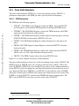
8.1.5 Four Transfer Activation Triggers
QSPI transfers are activated by any of four transfer triggers from the protocol timer or the
MCU. Each timer or MCU transfer trigger initiates a transfer of successive data from
RAM, starting at the address pointed to by the queue pointer for that trigger.
8.1.6 Programmable Delay after Transfer
Some serial peripherals require additional chip-select hold time after a transfer is
completed. To simplify the interface to these devices, a delay of 1 to 128 serial clock
cycles between queues can be programmed at the completion of a queue transfer.
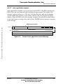
8.1.7 Loading a Programmable Address at the End of Queue
A queue can be configured so that its last data entry is written to its queue pointer, thus
programming the start address for the next queue trigger from the queue itself. This
enables wrapping to the beginning of the queue or branching from one sequence to
another when a new transfer trigger activates the queue.
8.1.8 Pause Enable at Queue Entry Boundaries
A queue transfer can be programmed to terminate at queue entry boundaries by inserting a
PAUSE command in the control halfword of the queue entry at that boundary. This
feature enables each of the four transfer triggers to provide programmable multiple-task
support and considerably reduces MCU intervention.
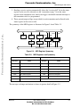
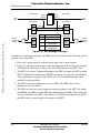
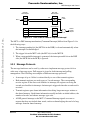
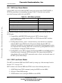
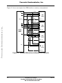
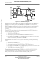
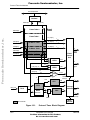
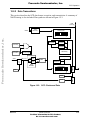
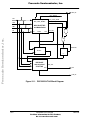
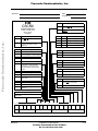
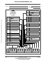
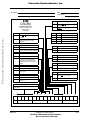
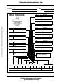
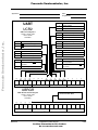
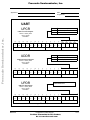
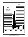
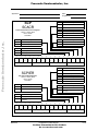
8.2 QSPI Architecture
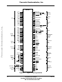
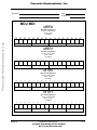
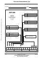
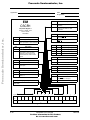
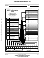
This section describes the QSPI pins, control registers, functional modules, and
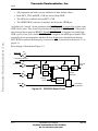
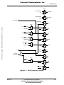
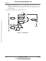
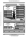
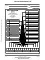
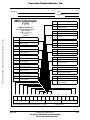
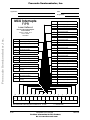
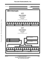
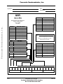
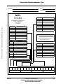
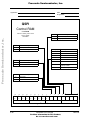
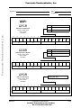
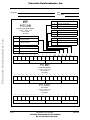
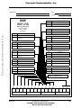
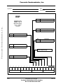
special-purpose RAM. Most of these components are shown in the QSPI flow diagram in
Figure 8-1.
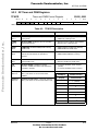
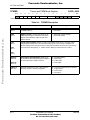
The QSPI port can also function as GPIO, which is governed by three control registers
that are also described.
Motorola
Queued Serial Peripheral Interface
For More Information On This Product,
Go to: www.freescale.com
8-3