1
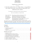
AD7280 Capability Demonstration
A Major Qualifying Project
Submitted to the Faculty
of the
WORCESTER POLYTECHNIC INSTITUTE
in partial fulfillment of the degree requirements for the
Degree of Bachelor of Science
in
Electrical and Computer Engineering
by
____________________________
Alex Levy
____________________________
Shaun Tirrell
____________________________
Jieyu Wu
Project Number: AW-001
Date: 10/19/08
Sponsoring Organization:
Analog Devices, Inc.
Project Advisors:
____________________________
Professor Alexander Wyglinski, Advisor
____________________________
Professor Richard Vaz, Advisor
Abstract
This report presents a demonstration product created for Analog Devices, Inc.'s AD7280. The
AD7280 is a lithium ion battery monitoring system that typically uses several chips in series. This design
makes use of an array of current mirrors to allow the AD7280s to be used in parallel. A GUI was also
created to allow user interaction. Finally, a battery simulation was created so that adjustable inputs could
be applied to the system, thus greatly improving the effectiveness of the demonstration.
Page 2 of 278
Acknowledgments
This project would not have been as successful if it were not for a number of individuals whose
assistance and guidance helped the project move along as smooth as possible. Whether it be assisting
us with a certain aspect of the project, providing guidance, or simply making sure we were comfortable,
their help was greatly appreciated. While we can‟t be sure we‟ve thanked everyone, the following is at
least a partial list of those individuals and organizations who were especially deserving of recognition for
their help and support they provided during our time in Limerick.
We would like to thank Analog Devices, Inc. for sponsoring this project and giving us this opportunity.
We would especially like to thank John Reidy for acting as our primary liaison and coordinator throughout
the project. A very special thanks to Shane Rabbitte whose help and guidance were essential to the
project. Additionally, his help with getting us acclimated to the company environment was greatly
appreciated. We would also like to thank John Wynn, Ger Blaney, Claire Leahey and the entire test
engineering group for their help and resources that they provided. These people helped the project go as
smooth as possible.
Thanks to Declan Burke and Litho Circuits for doing the layout and assembly of our PCB. A Special
thanks to Declan for mediating between us and the manufacturing center, and for completing the layout
as quickly as possible.
Thank you to Bright Solutions Ltd for repeatedly fixing our evaluation boards when they were broken.
They were very accommodating and fixed the boards as fast as possible.
Of course, thank you to Worcester Polytechnic Institute and especially the Interdisciplinary and Global
Studies Division for giving us this great opportunity and arranging all the details that allowed this project
to happen. A special thanks to Professor Alexander Wyglinski and Professor Richard Vaz for advising us
during this project. Their frequent correspondence and weekly teleconferences provided the guidance
and challenges we needed to maintain a high level productivity. Additionally, their enthusiasm and
positive attitudes helped to make what we thought was a great Major Qualifying Project experience.
Page 3 of 278
Finally, thank you to Charlotte Tuohy for all of her help. Charlotte secured our living arrangements,
and made sure we had everything we needed upon arrival to Ireland. She was always helpful whenever
we needed anything, and really helped make our time in Limerick as comfortable as possible.
Page 4 of 278
Executive Summary
It is known that the world's fossil fuel supply is running out. There are also many
environmental hazards associated with the use of and drilling for fossil fuels. One solution to these
problems is hybrid cars. Hybrid cars run on a combination of gasoline and rechargeable batteries. This
increases fuel mileage and reduces the total amount of fossil fuels that is needed per hybrid car. One
new and efficient kind of rechargeable battery that can be used in hybrid cars are lithium-ion batteries.
However, these batteries are not perfect and need to be monitored due to certain complications that can
result from low charge, over charge, low temperature, or high temperature.
The company Analog Devices, Inc has come up with a device called the AD7280 that
serves exactly this purpose. The AD7280 is an analog to digital converter that can monitor the
temperature and charge of six lithium-ion battery cells. A typical hybrid car would use one hunderd of
these lithium-ion battery cells to help power the vehicle. A fully charged lithium-ion battery cell has up to
a four-volt potential meaning the series addition of all 100 battery cells can be up to 400 volts. The
AD7280 is capable of monitoring up to 5000 of these cells using its ability called the daisy chain. In
typical applications, such as in a hybrid car, 100 battery cells are used. In the daisy chain mode, the
devices are connected in a series configuration and communicate on seven data lines using current as
signals. They run on a differential voltage with the total absolute voltage being 400 volts. This means
that when Analog Devices tries to demonstrate the AD7280 to potential customers, a 400-volt supply is
required to present the product's full capabilities. Such a high voltage supply causes complications with
safety and portability. Our project is to create a system that can show off the capabilities the AD7280 and
eliminate the safety and portability complications.
The solution to this high-voltage demonstration problem, and the major design problem of
this project, is to rearrange the configuration and put the AD7280s in parallel, meaning all of them run on
the same, lower voltage. This was accomplished using a current mirror circuit that allows the current
signal data to be mimicked across different voltage levels. Two AD7280s would remain in series to prove
that the concept works while the next two AD7280s are in parallel with the previous two, communicating
through the current mirrors. Since the parallel configuration only requires enough voltage to run two
AD7280s plus the current mirrors, a supply of only 51 volts is needed to operate an arbitrary number of
AD7280s. The two AD7280s in series will use 45 volts as Vdd while the current mirrors operate at three
volts outside of ground and Vdd, totaling 51 volts. This is a great improvement over the 400 volt supply
required for the series configuration with respect to both safety and portability as a much smaller supply is
possible.
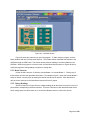
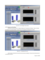
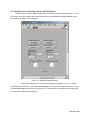
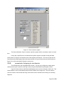
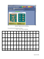
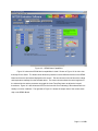
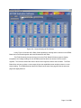
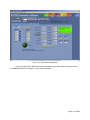
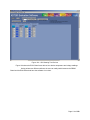
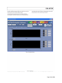
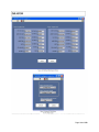
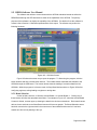
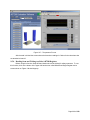
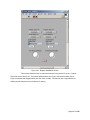
Another major part of our system was designing a graphical user interface (GUI). The
GUI needed to be presentable and easy to read to maximize the effectiveness of a demonstration. The
final GUI was designed using the National Instruments LabVIEW software. The design can be displayed
and interfaced with on a computer. It is capable of displaying all the capabilities of the AD7280s in a user
friendly manner. This GUI shows all the voltages being read from the battery cells, their temperature
readings, all of the control registers, and some alert indicators. This GUI allows the user or the presenter
to modify and read all the control registers to show the behavior of the AD7280s under any conditions
Page 5 of 278
desired. The software communicates to the AD7280s through the USB and a development board. The
development board is connected to a demonstration board containing the AD7280s, which was also
designed for this project, through a 96-pin connector.
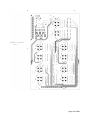
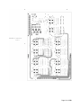
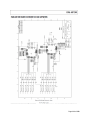
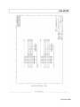
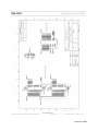
The demonstration board is a PCB that was designed to have the AD7280s in the parallel
configuration as previously described. It has a total of ten AD7280s and four current mirror circuits
connecting the AD7280 series pairs together. Along with an additional driver board, the demonstration
board can perform the previously stated functions with all of the functionality and components
consolidated into two boards. The driver board connects to the demonstration board through a 64-pin
connector. It acts as the lithium-ion battery cells that the AD7280 monitors by controlling the voltage that
is read by the AD7280s using resistors. There are also a set of potentiometers on the driver board that
are used to adjust resistances to show the AD7280's ability to read a range of voltages. It also has the
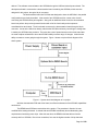
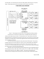
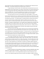
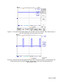
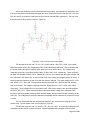
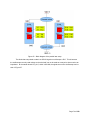
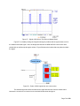
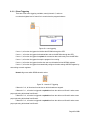
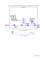
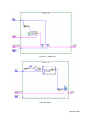
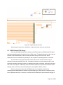
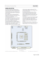
ability to measure current going through the system. Figure 1 shows a top level block diagram of the
whole system.
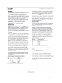
Figure 1 – System-level block diagram of our project
With the demonstration PCB and driver board, an effective showcase of the AD7280's capabilities
can be done.
The DEMO board PCB was received late in the project. The procedure in Section 9.6 was
modified before testing the board. It worked with two AD7280s immediately but troubleshooting was
required when introducing more chips. After this was done, the DEMO board was able to function
correctly with four AD7280s. Due to time constraints, four was the highest number of chips that were
Page 6 of 278
tested. Since each of the current mirrors and AD7280 pairs are in parallel, the DEMO board will work with
ten AD7280s, as intended. The driver board that was built to drive the DEMO board inputs was
successfully completed and enclosed in a box with potentiometer knobs and a 64-pin connector. This
had to be converted to drive the AD7280 EVAL board for two reasons. First, time constraints prevented
the DEMO board from being fully tested, and second, post-manufacturing rework which caused the
DEMO board to no longer be as presentable as would be required for a marketing presentation. The
converted driver board, EVAL board, and GUI were then all used into the system. When this was done,
the software correctly read the adjustable voltages given to it by the driver board and the GUI performed
as intended.
Page 7 of 278
Contents
Abstract ......................................................................................................................................................... 2
Acknowledgments ......................................................................................................................................... 3
Executive Summary ...................................................................................................................................... 5
Contents ........................................................................................................................................................ 8
Table of Figures .......................................................................................................................................... 12
Table of Tables ........................................................................................................................................... 15
1.
2.
Introduction .......................................................................................................................................... 16
1.1.
Project Objectives ................................................................................................................... 19
1.2.
Vision....................................................................................................................................... 19
1.3.
Specific Technical Goals ......................................................................................................... 19
Background Research ......................................................................................................................... 22
2.1.
Li-ion Battery Technology ....................................................................................................... 22
2.2.
Thermistors ............................................................................................................................. 24
2.3.
Analog to Digital Converters ................................................................................................... 24
2.4.
The AD7280 ............................................................................................................................ 27
2.5.
LabVIEW ................................................................................................................................. 30
2.6.
Converter Evaluation & Development Board .......................................................................... 32
2.7.
AD7280 Evaluation Board ....................................................................................................... 32
2.8.
Current Mirrors ........................................................................................................................ 34
2.9.
Chapter Summary ................................................................................................................... 35
3.
Project Planning .................................................................................................................................. 37
4.
System Specifications ......................................................................................................................... 38
5.
4.1.
Overview ................................................................................................................................. 39
4.2.
System-Level Inputs ................................................................................................................ 40
4.3.
System-Level Outputs ............................................................................................................. 41
4.3.1.
Driver Board Outputs ................................................................................................. 41
4.3.2.
DEMO Board Outputs ................................................................................................ 41
4.3.3.
CED Board Outputs ................................................................................................... 42
4.3.4.
Laptop Running GUI .................................................................................................. 42
Design Methods .................................................................................................................................. 43
5.1.
Product Requirements ............................................................................................................ 43
Page 8 of 278
5.2.
DEMO Board ........................................................................................................................... 44
5.3.
Driver Board ............................................................................................................................ 44
5.4.
Parts Selection ........................................................................................................................ 46
5.5.
6.
5.4.1.
Current Mirrors ........................................................................................................... 47
5.4.2.
Driver Board Components ......................................................................................... 47
5.4.2.1.
XP Power AED36US48 Power Supply ....................................................... 48
5.4.2.2.
AD817 High Current Opamp ...................................................................... 48
5.4.2.3.
TL783 Adjustable Voltage Regulator.......................................................... 48
5.4.2.4.
ADP3338 3.3V Voltage Regulator .............................................................. 48
5.4.2.5.
MAX660 Voltage Converter ........................................................................ 49
Software Development ............................................................................................................ 49
5.5.1.
Board Selection.......................................................................................................... 50
5.5.2.
Voltage Readings ...................................................................................................... 50
5.5.3.
Temperature Readings .............................................................................................. 51
5.5.4.
Reading from and Writing to all the AD7280 Registers ............................................. 52
5.5.5.
Automatically Configuring the Alert Function ............................................................. 54
5.5.6.
Save All Converted Data ........................................................................................... 55
5.5.7.
Show 10 Chips ........................................................................................................... 57
5.5.8.
Selectable Detailed Display of all Devices ................................................................ 57
Implementation/Results ....................................................................................................................... 59
6.1.
6.2.
Testing..................................................................................................................................... 59
6.1.1.
Initial Series Testing .................................................................................................. 59
6.1.2.
Current mirror verification. ......................................................................................... 65
6.1.3.
Initial Parallel Testing ................................................................................................. 72
6.1.4.
EVAL Board Final Testing ......................................................................................... 79
Software Implementation ........................................................................................................ 83
6.2.1.
Examining the Lower Level Code .............................................................................. 84
Page 9 of 278
6.2.1.1.
Event Triggering ......................................................................................... 85
6.2.1.2.
Button Triggering Event .............................................................................. 86
6.2.1.3.
Runtime-Actions ......................................................................................... 88
6.3.
DEMO Board PCB Design .................................................................................................... 101
6.4.
DEMO Board Troubleshooting .............................................................................................. 102
6.5.
Driver Board Build ................................................................................................................. 105
6.6.
Driver Board Troubleshooting ............................................................................................... 107
6.7.
Interfacing the Driver Board with the EVAL Board ................................................................ 107
7.
Recommendations/Future work ........................................................................................................ 108
8.
Conclusions ....................................................................................................................................... 110
9.
Appendix ........................................................................................................................................... 115
9.1.
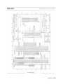
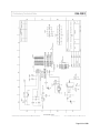
DEMO Board Schematics ..................................................................................................... 115
9.2.
DEMO Board PCB Layout..................................................................................................... 138
9.3.
Driver Board Schematics ...................................................................................................... 153
9.4.
Datasheets ............................................................................................................................ 157
9.5.
9.4.1.
AD7280 Lithium Ion Battery Monitoring System Datasheet .................................... 157
9.4.2.
EVAL Board Datasheet ............................................................................................ 190
9.4.3.
CED Datasheet ........................................................................................................ 210
9.4.4.
BCV61 NPN Current Mirror ..................................................................................... 234
9.4.5.
BCV62 PNP Current Mirror...................................................................................... 240
9.4.6.
AD8210 Current Shunt Monitor Datasheet .............................................................. 248
DEMO Software User Manual ............................................................................................... 264
9.5.1.
Board Selection........................................................................................................ 264
9.5.2.
Voltage Readings .................................................................................................... 265
9.5.3.
Temperature Readings ............................................................................................ 265
9.5.4.
Reading from and Writing to all the AD7280 Registers ........................................... 266
9.5.5.
Automatically Configuring the Alert Function ........................................................... 269
9.5.6.
Save All Converted Data ......................................................................................... 270
9.5.7.
Show 10 Chips ......................................................................................................... 271
Page 10 of 278
9.5.8.
Selectable Detailed Display of all Devices .............................................................. 272
9.6.
DEMO Board Test Procedures ............................................................................................. 273
9.7.
Driver Board Test Procedures............................................................................................... 275
10. References ........................................................................................................................................ 276
Page 11 of 278
Table of Figures
Figure 1 – System-level block diagram of our project ................................................................................... 6
Figure 2 – Hybrid car. The blue section in the back of the car is the gas tank. The large yellow and black
box block in the center of the vehicle is the battery bank. The grey cylindrical object is the electric motor.
The yellow block represents the gas engine. Finally, the green object represents the transmission of the
vehicle. Reprinted with permission from [1]. .............................................................................................. 18
Figure 3 – Gas car. The colored sections of the vehicle represent the same objects as in Figure 2. Note
the lack of the battery, as well as the electric motor it would power if either were present. Reprinted with
permission from [1]...................................................................................................................................... 18
Figure 4 – Series configuration of the AD7280. This is the configuration that will be used in a real-world
application. .................................................................................................................................................. 20
Figure 5 – Parallel configuration of the AD7280. This is the configuration that our project intends to utilize.
.................................................................................................................................................................... 21
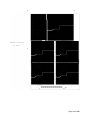
Figure 6 – Chart of capacity vs. cell voltage. Note the particularly sharp knee on the li-ion cell as it nears
full discharge compared with other technologies. Reprinted with permission from [2]. ............................. 23
Figure 7 – Simple voltage divider network with a resistor and a thermistor. As the temperature of the
thermistor varies, so too will it‟s resistance, and thus the voltage output will fluctuate. Note that the
indicated value of 10k on the thermistor is a nominal resistance, and will vary as described in the
product‟s datasheet. .................................................................................................................................... 24
Figure 8 – Block diagram describing an ADC. ............................................................................................ 25
Figure 9 – Three-bit ADC output. Compare the dotted line, indicating an ideal transfer function, with the
solid black line that indicates the actual output code with three-bit accuracy............................................. 25
Figure 10 – Three-bit ADC with a ½ bit offset inherent in the design. The dotted line is an ideal transfer
function, as in Figure 9, and the solid line indicates the code interpreted by the ADC. ............................. 26
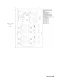
Figure 11 – Block diagram representation of the AD7280, including inputs and outputs. Reprinted from
[3] with permission. ..................................................................................................................................... 27
Figure 12 – Functional representation of the daisy chain interface used by the AD7280. Modified from [3]
with permission. .......................................................................................................................................... 28
Figure 13 – SubVI call ................................................................................................................................. 30
Figure 14 – LabVIEW adder code ............................................................................................................... 31
Figure 15 – Some LabVIEW displays ......................................................................................................... 31
Figure 16 – Block Diagram for the CED Board. Reprinted from [4] with permission. ................................ 32
Figure 17 – Block diagram of the EVAL board. Figure reprinted from [5] with permission. ....................... 33
Figure 18 – NPN (left) and PNP (right) current mirrors. .............................................................................. 34
Figure 19 – Current mirror pair. .................................................................................................................. 35
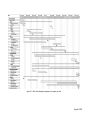
Figure 20 – Gant chart showing the progress of our project over time ....................................................... 38
Figure 21 – System-level block diagram of the project. .............................................................................. 40
Figure 22- System Level Diagram .............................................................................................................. 41
Figure 23 – DEMO Board Block Diagram ................................................................................................... 42
Figure 24 – CED Board Block Diagram ...................................................................................................... 42
Figure 25 – System Block Diagram of GUI and Computer ......................................................................... 42
Figure 26 – Current mirror input to the adjustable resistor network. The supply to the system is +48V,
which is much higher than the current mirror can accept. We bring the effective voltage down by using
two 20V zener diodes in series, and then dropping the remainder of the voltage across a resistor. This
ensures that the current going through I_INPUT is constant. Second order effects add non-idealities that
were small enough for our project that we ignored them. ........................................................................... 46
Figure 27 – Current mirror schematics for the BCV61 and BCV62, manufactured by Infineon. ................ 47
Figure 28 – GUI Main Screen ..................................................................................................................... 50
Figure 29 – Cell Voltage Value Screen ....................................................................................................... 51
Figure 30 – Temperature Screen .................................................................................................................. 51
Figure 31 – Register Read/Write Screen .................................................................................................... 52
Figure 32 – How to select a device ............................................................................................................. 53
Page 12 of 278
Figure 33 – How to select a register ........................................................................................................... 54
Figure 34 – Button to click on to configure alert condition .......................................................................... 55
Figure 35 – Button to click on to save data ................................................................................................. 56
Figure 36 – showing 60 cell voltage and temperature readings ................................................................. 57
Figure 37 – All capabilities of the AD7280 are displayed on this screen. ................................................... 58
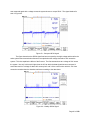
Figure 38 – This picture shows what happens when the Alert Test Point Is Probed. Alert can either be a
high or low, and on this picture it is a high. ................................................................................................. 59
Figure 39 – This picture shows what happens when the CNVST Test Point Is Probed. CNVST is either a
high or a low, and in this picture it is a high. ............................................................................................... 60
Figure 40 – This picture shows what happens when the CS test point is probed. Chip Select is active low
and is pulled low periodically. ..................................................................................................................... 60
Figure 41 – This picture shows what happens when the PD Test Point Is Probed. PD is either a high or a
low and is active high, and in this picture it is a high. ................................................................................. 61
Figure 42 - This picture shows what happens when the SCLK Test Point Is Probed. During operation, the
PFGA sends bursts of clocks periodically. We see that a 1 MHz clock is being busted every
approximately. 30ms ................................................................................................................................... 61
Figure 43 – This picture shows what happens when the SDIhi SDOlo Test Point Is Probed with 10ms time
scale with 10ms time scale. Every few 20 to 30ms, a stream of bits is sent. ............................................ 62
Figure 44 – This picture shows what happens when the SDIlo SDOhi Test Point Is Probed with 10ms time
scale. Every few 20 to 30ms, a stream of bits is sent. ............................................................................... 62
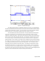
Figure 45 – Data array from CED with Turning off Temperature Readings to Collapse the Data Stack.... 63
Figure 46 – Data array from CED before problem fixed without with Turning off Temperature Readings to
Collapse the Data Stack.............................................................................................................................. 63
Figure 47 – Data array from CED after problem fixed ................................................................................ 64
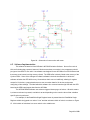
Figure 48 – NPN (left) and PNP (right) current mirror test circuits ............................................................. 65
Figure 49 – First full current mirror experiment ........................................................................................... 66
Figure 50 – Second full current mirror experiment ..................................................................................... 67
Figure 51 – Third full current mirror experiment.......................................................................................... 68
Figure 52 – First current mirror circuit using all seven data lines. .............................................................. 69
Figure 53 – Second current mirror circuit using all seven data lines. Send signal connected to the base of
the receiving current mirror transistor ......................................................................................................... 71
Figure 54 – Test integration of current mirrors............................................................................................ 73
Figure 55 – Block diagram of the parallel test setup. .................................................................................. 74
Figure 56 – Data from the master board (top) and the slave board (bottom). Note that the slave is not
receiving data. ............................................................................................................................................. 75
Figure 57 – Signal of SCLK from Test Point on Master Board ................................................................... 76
Figure 58 – Probe of SCLK signal after one current mirror ........................................................................ 76
Figure 59 – Picture of SCLK test point output from the Master Board ....................................................... 78
Figure 60 – Signal of SCLK Signal after One Current Mirror ...................................................................... 78
Figure 61 – SCLK from the slave board...................................................................................................... 79
Figure 62 – Healthy SCLK Signal ............................................................................................................... 80
Figure 63 – Corrupted SCLK signal ............................................................................................................ 81
Figure 64 – Healthy SDOlo Signal .............................................................................................................. 81
Figure 65 – Corrupted SDOlo Signal .......................................................................................................... 82
Figure 66 – Schematic of current mirror with zener. ................................................................................... 83
Figure 67 – Read/Write Single Register triggering ..................................................................................... 84
Figure 68 - VI Hierarchy .............................................................................................................................. 84
Figure 69 - num triggering ........................................................................................................................... 85
Figure 70 - Numeric 5 Triggering ................................................................................................................ 85
Figure 71 - Autorun Triggering .................................................................................................................... 87
Figure 72 - Initialize Triggering ................................................................................................................... 87
Figure 73 - Autoconfig Registers Triggering ............................................................................................... 87
Page 13 of 278
Figure 74 - Read/Write Single Register Triggering ..................................................................................... 88
Figure 75 - Board Action Buttons Triggering............................................................................................... 88
Figure 76 - CED Init .................................................................................................................................... 88
Figure 77 - After CED Init ............................................................................................................................ 89
Figure 78 - Prepare Data ............................................................................................................................ 89
Figure 79 - I/O config ................................................................................................................................. 90
Figure 80 - Manual Send to ....................................................................................................................... 91
Figure 81 - Simple Write ............................................................................................................................ 92
Figure 82 -– Simple write ............................................................................................................................ 93
Figure 83 - write ......................................................................................................................................... 93
Figure 84 – Calling Read Write Single ...................................................................................................... 94
Figure 85 – Read part of Read Write Single ............................................................................................. 94
Figure 86 – Write part of Read Write Single.............................................................................................. 95
Figure 87 – Write Reg ................................................................................................................................ 95
Figure 88 – Read Reg ................................................................................................................................ 96
Figure 89 – Simple Read ........................................................................................................................... 97
Figure 90 – Upload ..................................................................................................................................... 97
Figure 91 – Autoconfig loop ........................................................................................................................ 98
Figure 92 – Upload data and place data into array .................................................................................... 98
Figure 93 – Calculate voltages and temperatures from code ................................................................... 100
Figure 94 – Append all data and save ...................................................................................................... 101
Figure 95 – A picture of the DEMO board without any chips inserted into the clamps. ........................... 102
Figure 96 – Screenshot of two out of four boards working ....................................................................... 104
Figure 97 – Screenshot showing all four devices working properly .......................................................... 105
Figure 98 – A schematic representation of the resistor network we set up for the adjustable voltage
outputs. As R3 increases, the total resistance increases, leading to a larger voltage drop across the
combination of three resistors at constant current. ................................................................................... 106
Figure 99 – Current mirror setup used to control the current going through the adjustable resistor network.
A constant current was required in order to allow one output to vary without affecting the others. ......... 106
Figure 100 – Finalized Front Page ............................................................................................................ 110
Figure 101 - DEMO Board Capabilities..................................................................................................... 111
Figure 102 – Screen Showing All Ten Devices......................................................................................... 112
Figure 103 – EVAL Board Capabilities ..................................................................................................... 113
Figure 104 – GUI Showing Two Devices .................................................................................................. 114
Figure 105 – GUI Main Screen ................................................................................................................. 264
Figure 106 – Cell Voltage Value Screen ................................................................................................... 265
Figure 107 – Temperature Screen .............................................................................................................. 266
Figure 108 – Register Read/Write Screen ................................................................................................ 267
Figure 109 – How to select a device ......................................................................................................... 268
Figure 110 – How to select a register ....................................................................................................... 269
Figure 111 – Button to click on to configure alert condition ...................................................................... 270
Figure 112 – Button to click on to save data ............................................................................................. 271
Figure 113 – showing 60 cell voltage and temperature readings ............................................................. 272
Figure 114 – shows all capabilities of AD7280 in one screen. ................................................................. 273
Page 14 of 278
Table of Tables
Table 1 – Listing of the AD7280‟s daisy chain communication pins. .......................................................... 28
Table 2 – List of registers in the AD7280. Table continues on next page. ................................................ 29
Table 3 – Address labels for AD7280 ......................................................................................................... 30
Table 4 – Listing of requirements for ADI and potential customers. ........................................................... 39
Table 5 – How to read the saved data ........................................................................................................ 56
Table 6 – Results of the experiment shown in Figure 52 ............................................................................ 70
Table 7 – Results of the experiment shown in Figure 53............................................................................ 72
Table 8 – How to read the saved data ...................................................................................................... 271
Page 15 of 278
1. Introduction
Over the past several years, it has become evident that the Earth's natural fossil fuel resources
are starting to reach what is known as peak oil, [6] or Hubbert's Peak [7]. M. King Hubbert first proposed
in 1956 that eventually, due to the irreplaceability of fossil fuels, we would eventually reach a point where
oil production drops off not because of reduced demand for energy, but because of physical limits on how
much can be extracted from the ground. Crude oil prices have skyrocketed over the past ten years,
climbing close to 700% in 2008 dollars [8]. Additionally, environmental concerns have begun to
encourage conservation efforts both in the United States and abroad.
Environmental concerns exist for both the use of, and drilling for, fossil fuels. A fossil fuel is
defined as "An energy source formed in the Earth's crust from decayed organic material. The common
fossil fuels are petroleum, coal, and natural gas” [9]. They are drilled for and mined in various locations
throughout the world. There are several environmental concerns regarding the drilling for fossil fuels. For
one, it is possible to corrupt the ground water supply as "drilling can break the barrier between fossil fuel
and groundwater reserves" [10]. It can also harm the physical environment and existing plants and
wildlife because “when oil and gas are removed from a reserve under the earth, this leaves what is
essentially a large hole underground. When there is no longer anything to support the land above, the
land can collapse" [10]. Additionally there have been known to be complications and oversights with the
handling of fossil fuels as “oil can enter the sea from spent drilling sites [and] oil refineries can also
discharge oil into the environment as waste" [11]. These concerns with the actual acquiring of fossil fuels
are not the only ones that exist when is comes to the overall use of fossil fuels.
There are also environmental concerns with the burning and combustion of fossil fuels. The
combustion of fossil fuels emits carbon dioxide which “is considered a greenhouse gas as it traps heat
(infrared energy) radiated by the Earth into the atmosphere and thereby contributes to the potential for
global warming" [12]. Additionally, “burning fossil fuels also releases sulphur (sic) dioxide and nitrogen
oxides. These gases contribute to the greenhouse effect, form acid rain, and can make the air unhealthy
to breathe in urban areas where their concentrations are normally highest" [11]. All of these
environmental concerns are on top of the fact that the world fossil fuel reserves are running low. At the
rate of consumption in 2003 and with the amount of fossil fuels left on the planet, there remains
approximately 1,000 billion barrels of oil, enough to last 38 years, 5,400 trillion cubic feet of natural gas,
enough to last 59 years, and 1,000 billion metric tons of coal, enough to last 245 years [10]. Obviously
with these supply concerns in addition to the environmental hazards, a solution needs to be found. One
of the solutions is hybrid vehicles.
It is a known fact that hybrid vehicles use fuel more economically then a standard car. Of the
three most common forms of fossil fuels, petroleum, the fuel used by cars, “ranked a close second
(behind coal) as a source of carbon dioxide emissions from the consumption and flaring of fossil fuels in
2005, accounting for 39.0 percent of the total” [13]. This total is 28192.74 million metric tons [14] of
carbon dioxide emitted worldwide in 2005. In a study done at the Massachusetts Institute of Technology
(MIT), it was found that “hybrids, plug-in hybrids, and other advanced vehicle systems could be
incorporated into the U.S. fleet rapidly enough to make a significant dent in total fuel use by 2035" [15].
Page 16 of 278
This has the caveat that great efforts are made to “increase the [emphasis on reducing fuel consumption],
increase the market penetration rate of advanced propulsion technologies, and find ways to reduce the
rate of growth in demand” [15]. If these things are done, say the MIT researchers, the “total fuel use in
2035 could end up being less than half what it would be if we take no action, with greenhouse gas (GHG)
emissions reduced by almost as much” [15].
It is anticipated that as the population continues to grow and demand for energy climbs ever
higher, gas prices and environmental concerns will play increasingly more important roles in modern
society. One of the most visible solutions in American society is the hybrid electric vehicle (HEV) that
came into prominence in August 2000 with the launch of the Toyota Prius. The 2008 model of the Prius
gets 48 miles per gallon (mpg) city driving, 45 mpg highway [16], while the 2008 national average in the
United States is 24.8 mpg [17]. With such a large gap in mpg between the average car and the
possibilities of hybrid cars, it follows that hybrid vehicles can potentially help to solve the world's energy
crisis.
While there are several different variations on exactly how it is achieved, all HEVs rely upon a
gasoline engine to supplement power to a battery-powered electric motor, and also to recharge the
battery when the energy stored in it has become depleted. See Figure 2 for a pictorial description of the
power train of a hybrid vehicle. Note that electric motors are at their most efficient at low speeds [18],
while gasoline internal combustion engines are very efficient at high speeds [19], so combining the two
allows for maximum gas mileage. Additionally, HEVs are able to partially recharge their batteries during
braking by effectively running the electric motor in reverse, thus producing a current into the battery [20].
Given that HEVs are reliant upon batteries, and that moving a mass as large as a car requires a
large amount of energy, a high capacity, fast-recharging, stable, safe battery is required. For the
moment, the industry has decided upon lithium ion (li-ion) battery technology to fulfill this need. Li-ion
technology has relatively lightweight materials, high energy density, provides large instantaneous power
supply, does not exhibit a memory effect1, and allows for many charge/discharge cycles without aging.
1
A memory effect is a term generally used to describe how NiMH and NiCd batteries lose
capacity when they are not completely discharged before being recharged. A memory-like effect can also
be seen when batteries are overcharged, which causes them to experience what is known as a voltage
depression where the voltage provided by the battery drops quickly over time, even at low current draw.
Overcharging and the resulting voltage depression does not actually reduce the energy capacity of the
battery, but devices monitoring the batteries will falsely indicate that they need to be recharged before
they are truly out of energy.
Page 17 of 278
Figure 2 – Hybrid car. The blue section in the back of the car is the gas tank. The large yellow
and black box block in the center of the vehicle is the battery bank. The grey cylindrical object is the
electric motor. The yellow block represents the gas engine. Finally, the green object represents the
transmission of the vehicle. Reprinted with permission from [1].
Figure 3 – Gas car. The colored sections of the vehicle represent the same objects as in Figure 2. Note
the lack of the battery, as well as the electric motor it would power if either were present. Reprinted with
permission from [1].
However, there are several disadvantages to li-ion technology. First, due to the high energy
density, if manufacturing errors or high stresses occur, li-ion cells are prone to catching fire, and even
explosions [21]. In an automotive application, this is to be avoided at all costs. Additionally, while there is
no memory effect associated with lithium-based batteries, they do lose capacity as they age. At higher
temperatures, the aging process is particularly damaging [22]. Finally, there is no such thing as a deep
discharge2 li-ion battery. If the cells are discharged too far, they become unstable when recharged, and
again, they can explode. As a result, while li-ion batteries carry great potential, they need to be monitored
constantly to ensure that they are not damaged. For our project, we attempt to design a device intended
to demonstrate the capabilities of the AD7280, a chip manufactured by Analog Devices, Inc., which is
capable of monitoring both the voltage and temperature of up to six cells in a li-ion battery [3].
2
Deep discharge batteries are designed to be discharged to 20% or less of their total capacity.
Page 18 of 278
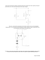
1.1. Project Objectives
The objectives of this project are to create a li-ion battery simulator that can effectively
demonstrate the capabilities of the AD7280 battery monitoring system during trade shows and in other
customer-sensitive environments. The AD7280 is manufactured by Analog Devices, Inc. (ADI). The true
application of this system uses 400 volts to monitor 100 individual 4-volt battery cells in a HEV. This
voltage is too high to be safely worked within a demonstration setting. In order for ADI to effectively and
safely demonstrate the capabilities of this product to potential customers, a lower voltage needs to be
used. To do this, the series configuration that builds up to a 400-volt or greater potential needs to be
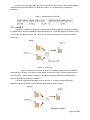
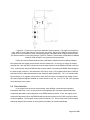
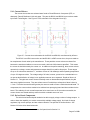
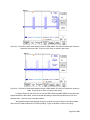
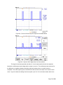
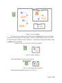
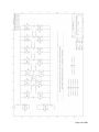
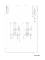
converted to a parallel configuration that uses a much lower (and safer) voltage. Referring to Figure 4,
notice that in the actual application each consecutive AD7280 is given inputs which are at a higher
voltage than the previous chip. Contrast this with Figure 5, the parallel configuration of AD7280s, which
allows us to monitor many cells at a safe voltage. Due to user interface, size, and weight considerations,
this project monitors only 60 cells instead of the anticipated 100 or more that would be used by an
automotive company. This new configuration will be laid out on a printed circuit board and will be
portable, with its own on board power supply to both power the monitoring system, and simulate the
battery voltages. The use of a USB interface between the system and computer software will be
investigated and applied if possible. The interface will be used to set the simulated voltages, as well as to
transmit data about the voltage and temperature outputs from the AD7280s. That data will then be
displayed on the computer screen. If a USB interface is not found to be feasible, another means will be
realized to control the voltage inputs to the AD7280s.
1.2. Vision
These objectives, when realized, will allow Analog Devices to demonstrate the full capabilities of
the AD7280. Our mission is to achieve these objectives by creating and designing a stand-alone printed
circuit board (PCB) that requires a voltage supply of less than 60 volts to monitor 60 cells and uses a
presentable GUI that will make the product appealing to the customer. The market base of the hybrid and
plug-in car industry continues to broaden, and by achieving our objectives we can contribute to the growth
of an evolving and globally important industry. In order to make inroads into the marketplace, though, a
working product needs to be developed and effectively marketed to major automotive suppliers. In our
case, a "working product" will be in the form of a device that can be brought to a trade show, or to a
customer's headquarters, and will demonstrate the ability of the AD7280 to monitor li-ion battery cell
voltage and temperature.
1.3. Specific Technical Goals
The goals we intend to fulfill follow. Our completed design must meet each of the following
design objectives:
Ability to be Safely Demonstrated - The final design will use no more than 60 volts. To do this,
the series of 60 cells application will be converted to a parallel application, which will allow each individual
board to have sufficient voltage and still be safe for demonstration.
Page 19 of 278
Durability - This device is going to be frequently transported and manipulated by non-experts
(customers and managers, among others). As such, it needs to be able to take a beating and still
perform to specification. We intend to accomplish this by having the board built professionally.
Clarity – Clarity is important for our project in two ways. First, after being introduced to the topic
there should be no question about what is being demonstrated. Second, the GUI should be easily
understood, including both the human computer interaction (HCI) and data output sections. This means
that people should not have difficulty understanding what the buttons on the GUI do, and they should be
able to understand what the GUI is displaying at all times.
Presentable Design - The PCB should be as small and as well laid out as possible. It should
also be able to use a portable power supply. Additionally, the device should appear professionally made.
User Interface - The battery monitoring device GUI should be presentable and appealing to
potential customers. To do this, the interface that was previously developed in LabVIEW will be modified
to account for both the new parallel configuration, as well as to show off the performance of the AD7280
in an eye-catching manner.
Adjustable voltage inputs - One major feature required by ADI is the ability to show off the
alarm features of the AD7280. If the cell voltage or temperature goes outside of the allowable ranges, the
AD7280 is supposed to raise alarm flags so that an outside micro-controller can take appropriate actions.
This is especially important when talking about li-ion batteries in the automotive industry, as li-ion
batteries have been known to catch fire. Obviously, this is to be avoided when driving down the highway
at 100 kph. The adjustable voltages are supposed to simulate both normal and alarm conditions, which
should be reflected by the GUI flashing warning lights. These voltage inputs are going to be supplied
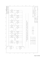
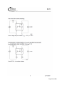
from what will be referred to as a driver board from now on.
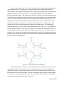
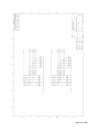
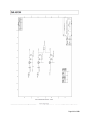
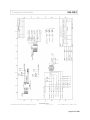
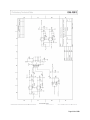
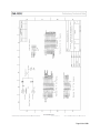
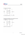
Figure 4 – Series configuration of the AD7280. This is the configuration that will be used in a real-world
application.
Page 20 of 278
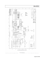
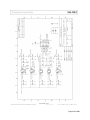
Figure 5 – Parallel configuration of the AD7280. This is the configuration that our project intends to utilize.
Page 21 of 278
2. Background Research
This chapter lists the various underlying technology of which our project makes use. It describes
each technology in sufficient detail that a person unfamiliar with the concept will be able to understand the
rest of the paper. Readers who are familiar with a given topic can feel free to move on to the next without
fear.
2.1. Li-ion Battery Technology
Batteries are an electrochemical energy storage system. They came into existence in the year
1800, created by Alexander Volta [23]. Batteries are made of one or more cells, each of which has the
basic elements of an anode, a cathode, and an electrolyte or separator which prevents the anode and
cathode from coming into direct contact. When discharging, electrons flow from the anode, though the
load, to the cathode. In a rechargeable battery, the opposite holds true during the charging cycle [24].
Including Volta‟s original battery, batteries have been created using such varied anode/cathode pairs as
zinc/silver [23], sponge metallic lead/lead dioxide (lead acid), cadmium/nickel oxyhydroxide (NiCd), rare
earth metal/nickel oxyhydroxide (NiMH), and many other chemicals [25].
Each combination has its own particular advantages and disadvantages. Some chemistries have
higher voltages (corresponding to higher energy density), some are able to provide higher currents for
longer periods of time without voltage drop, and some are lighter or can be manufactured more easily
than others. Of course, depending on the materials and processes used to construct the batteries,
different batteries will have higher costs [25].
Batteries based upon lithium metal were first proposed in 1912 [26]. These batteries were nonrechargeable, and did not even become commercially available until the 1970‟s [26]. When rechargeable
lithium metal batteries were investigated during the 1980‟s, safety problems plagued the research, and
the products were never successfully released [26]. The problem with lithium-based batteries is that,
along with being the lightest metal, lithium metal has the single highest energy density. When repeated
charging and discharging of the batteries caused changes on the lithium anode, which in turn reduced the
thermal stability of the battery [26]. Quoting from [26], “When this occurs, the cell temperature quickly
approaches the melting point of lithium, resulting in a violent reaction called „venting with flame‟.”
In 1976, around the same time that lithium metal batteries were first commercially offered, the
lithium ion chemistry was put forth as another alternative [27]. The first commercial li-ion battery
appeared in 1991 [26]. While li-ion batteries have slightly lower energy density than lithium metal
batteries, they are much safer. Protection circuitry attached to each cell during manufacturing guarantees
that the cells will not overheat violently, thus preventing a safety hazard [24]. Example circuitry is a
temperature controlled switch that opens if the temperature grows too high. The opened switch does not
allow further current to flow, which reduces the heat buildup inside the battery. Alternatively, the battery
can be fitted with a membrane which punctures after a pressure buildup inside the battery. If this ever
happens, the battery is permanently damaged and cannot be used [22]. Some cells are believed to be
damaged during manufacture by small metal fragments puncturing the separator between the anode and
cathode. Growth of these puncture holes over time, many charge/discharge cycles, and many thermal
Page 22 of 278
expansions is believed to be the cause of the frequent reports of li-ion batteries catching fire or exploding
in laptops [21].
On top of limiting manufacturing errors, correct charging/discharging schemes are vital to the
safety and length of life of li-ion batteries. A nominally full li-ion cell will put out approximately 3.7V
(citation needed). If the cell is discharged below 2.5V, the internal protection on the battery will open and
cause the battery to appear dead [22]. Some specialized chargers are able to correct this phenomenon,
but if the cell voltage is below 1.5V, even special equipment such as this cannot be used for safety
reasons [22]. Additionally, for safety reasons, most protection circuitry on a li-ion cell does not allow a
charge over 4.2V [22].
As stated above, discharging li-ion batteries below a certain threshold is detrimental to their
lifetime. Additionally, it is very difficult to know when this threshold is approaching, as the
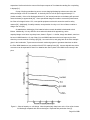
capacity/voltage curve has a very sharp knee, shown in Figure 6. A similar, though less drastic, trend can
be seen in NiMH batteries. On top of that, li-ion and NiMH batteries tend to have longer service lives
when they are not stored at full charge [22] [28]. As a result of this, and going back to the Prius example
given in the introduction, Toyota uses an electronic monitoring system to guarantee that does not allow
the Prius‟ NiMH batteries to vary outside of the 45-75% capacity limits [28]. It seems logical that a similar
occurrence can be expected for when li-ion batteries are used in place of the NiMH ones currently in the
prius.
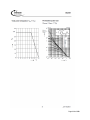
Figure 6 – Chart of capacity vs. cell voltage. Note the particularly sharp knee on the li-ion cell as it nears
full discharge compared with other technologies. Reprinted with permission from [2].
Page 23 of 278
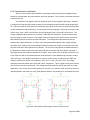
2.2. Thermistors
Thermistors are resistive devices whose resistance changes with temperature [29]. They can be
created with either positive or negative temperature coefficients. This makes them useful devices for
sensing temperature if the relationship between temperature and resistance is well known. For instance,
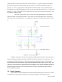
a voltage divider can be created using a resistor with a fixed value and a thermistor, as shown in Figure 7.
Assuming a positive temperature coefficient, as the temperature increases the thermistor resistance
increases, and so the voltage output will also increase proportional to the ambient temperature. This
output voltage can then be sent to a controller or microprocessor which can respond accordingly.
Figure 7 – Simple voltage divider network with a resistor and a thermistor. As the temperature of the
thermistor varies, so too will it‟s resistance, and thus the voltage output will fluctuate. Note that the
indicated value of 10k on the thermistor is a nominal resistance, and will vary as described in the
product‟s datasheet.
2.3. Analog to Digital Converters
The primary purpose of an analog to digital converter (ADC) is to convert analog signals to
discrete digital numbers in forms of bits [30]. This digital format can then be read by a microcontroller or a
computer. This device is seen in many monitoring systems such as battery voltage monitoring,
temperature monitoring, and others [3].
Some important concepts about the ADC include full scale voltage range, and resolution. Full
scale voltage range is the maximum analog input that can be placed upon the ADC [30]. Some typical
values on full scale voltage range ranges from 3 to 10 volts. Resolution is the number of discrete
representation the number of discrete values the ADC can produce over the range of analog values which
is based on the number of bits the ADC is capable of processing [30]. For example, a 2-bit ADC has 4 or
2^2 possible representations. If the full scale range of the ADC is 3 volts, this ADC will recognize analog
inputs of 0 volt, 1 volt, 2 volt, or 3 volts. Anything in between those 4 discrete points will be rounded to
the nearest level [30].
Page 24 of 278
Figure 8 – Block diagram describing an ADC.
So if the analog input is 2.7 volts, the 2 bit ADC will return a value of 3 Volts. And if the Analog
Input is 0.9 volts, the 2 bit ADC will return a value of 1 Volt.
The value that the ADC returns is usually in form of a code which represents a certain
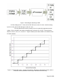
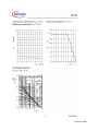
voltage. Given a 3 bit ADC, the number of possible return values are 2^3 or 8 [30]. These values are
000, 001, 010, 011, 100, 101, 110, and 111. Figure 9 shows a plot of these codes vs. the fractions of the
full scale resolution.
Figure 9 – Three-bit ADC output. Compare the dotted line, indicating an ideal transfer function, with the
solid black line that indicates the actual output code with three-bit accuracy.
Page 25 of 278
The dotted line in Figure 9 shows an ideal transfer function in which every representation in code
corresponds exactly to the appropriate analog input if the accuracy was infinite. The solid black line
indicates the actual output code for a given input at three-bit accuracy. However, since the accuracy is
limited, this transfer function rounds everything down causing a quantization error. For example when the
analog input voltage in Figure 9 is 1/9 of the full scale voltage range, the ADC will code this reading 000.
However, because 1/9 is much closer to 1/8 than 0, we need the ADC to code this reading as 001.
Therefore we introduce to the ADC a bit shift offset to deal with this. Figure 10 illustrates an example of
this offset.
Figure 10 – Three-bit ADC with a ½ bit offset inherent in the design. The dotted line is an ideal transfer
function, as in Figure 9, and the solid line indicates the code interpreted by the ADC.
Using the ½ bit shift, when the analog input voltage in the theoretical ADC indicated in Figure 10
is 1/16 and 3/16 of the full scale voltage range, the ADC will code this reading as 001. Similar readings
are made throughout the input range. The output of this theoretical ADC introduces a rounding of the
input to the nearest discrete representation.
Another important characteristic about ADCs is sampling to acquire data of the analog input
signal. The frequency at which the ADC samples at determines the rate at which new digital values are
acquired from the analog input signal. The higher the frequency with which the input signal changes, the
higher the sampling frequency is required by the ADC. The Nyquist theorem states that the ADC
sampling frequency must be at least twice the highest frequency inside the analog input signal [31].
Page 26 of 278
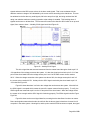
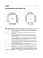
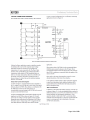
2.4. The AD7280
The AD7280 is a 12-bit ADC from ADI [3]. Its purpose is to monitor li-ion and NiMH
batteries. The AD7280 has six voltage inputs for six cell voltages as well as 6 thermistor inputs for
temperature monitoring of the cells. The analog inputs are ranged from 0 to 5 volts. The device has
configurable alert output which gives warning for situations in which the cells are not desired to be in such
as low voltage or over voltage, and high temperature. The device is powered by the input voltages
stacked together and it operates from 7.5V to 30V. The AD7280 communicates with a microcontroller
through serial interface via the SDIN and SDOUT pins [3].
The AD7280 also has an ability called the daisy chain. The daisy chain ability allows multiple
AD7280 to communicate with each other. Up to 50 devices can be linked together allowing for the
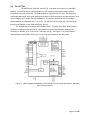
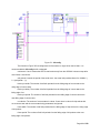
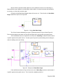
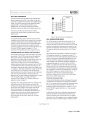
monitoring of 300 cells, up to 1110 volts (3.7 volts each cell) [3]. See Figure 11 for a block diagram
representation of the AD7280, and Figure 12 for a visual representation of the daisy chain.
Figure 11 – Block diagram representation of the AD7280, including inputs and outputs. Reprinted
from [3] with permission.
Page 27 of 278
Figure 12 – Functional representation of the daisy chain interface used by the AD7280. Modified
from [3] with permission.
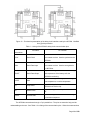
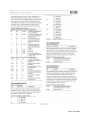
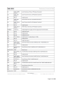
Table 1 – Listing of the AD7280‟s daisy chain communication pins.
Pin
Pin Name
Abbreviation
Pin Function
Input from the uProcessor which is transmitted
SCLK
Serial Clock
from master to slave. Used to synchronize the
AD7280s.
Input from the uProcessor which is transmitted
SDIN
Serial Data Input
from master to slave. Used to set registers in
the AD7280s.
Output containing information about the voltage
SDOUT
Serial Data Output
and temperature of the battery cells the
AD7280 is monitoring.
ALERT
Alert
CS
Chip Select
PD
Power Down
CNVST
Convert Start
Output indicating over-voltage, under-voltage,
over-temperature, or under-temperature.
Input indicating whether or not the relevant
AD7280 is the active chip.
Input indicating that the chip should shut itself
off.
Input indicating when the AD7280 should begin
a conversion sequence.
The AD7280s communicate through a 7-pin parallel bus. The pins are named to help provide
understanding to the user. See Table 1 for a listing of the communication pins. When the master strobes
Page 28 of 278
CNVST, the slave converts the data from the inputs attached to the slave and sends this data from the
SDOUT pin to the master.
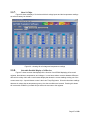
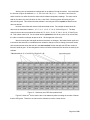
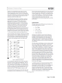
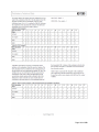
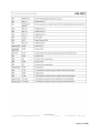
Each AD7280 device has the registers listed in Table 2.
Table 2 – List of registers in the AD7280. Table continues on next page.
Registers CELL VOLTAGE 1 to CELL VOLTAGE 6 gives the voltage readings in code for cells 1
through 6, respectively. Similarly, registers CELL TEMP 1 to CELL TEMP 6 gives the thermistor readings
in code for cells 1 through 6. The registers OVER VOLTAGE, UNDER VOLTAGE, OVER TEMP, and
UNDER TEMP are user configured for conditions that the user feels the need to set off the ALERT
register. The CB TIMER 1 to CB TIMER 6 allows to the user to program individual ON times for each of
the Cell Balance outputs between 0 to 30 minutes with 1 minute resolution. Lastly, the PD TIMER allows
the device to power down after a certain period of being ON.
Page 29 of 278
During the use of the daisy chain, bits D23-D18 are used to select devices. Device select address
should be written and read LSB first [3]. Reference Table 3 for a complete listing of addressing
information.
Table 3 – Address labels for AD7280
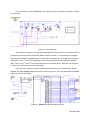
2.5. LabVIEW
LabVIEW is a platform for graphical programming developed by National Instruments that allows
the programmer to program embedded systems graphically [32]. A LabVIEW program is called a VI, and
a VI call other VIs during its runtime [32]. When a VI is called by another VI, the called VI is named a
SUBVI [32].
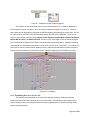
Figure 13 – SubVI call
Figure 13 shows that in the main VI, there are 3 variables (called Numeric in LabVIEW
nomenclature) A, B and C. The SUBVI named “SUBVI” is called in this main VI and this SUBVI takes 2
inputs and gives 1 output. So the 2 variables, A and B are provided as inputs for the SUBVI and the
output of the SUBVI is stored in the variable C.
Like other programming languages such as Java or C++, a platform compiler parses the
LabVIEW code and generates machine code that the platform CPU can execute.
Page 30 of 278
Figure 14 – LabVIEW adder code
Given the LabVIEW code shown on Figure 14, the equivalent C code for that would be int C, A,
B; C = A + B;. Basically the code in Figure 14 and the C code both tells an interpreter to take the value
stored in memory A and the value store in B and sum those 2 values and store the result to memory C.
The compiler would compile the LabVIEW code shown on Figure 14 to something that the CPU
can run the same way the C compiler compiles C code [33]. For our project, we used an X86 architecture
on a windows platform, so our compiler would create executable files from the LabVIEW code.
Similar to other programming languages such as C, C++, and Java, LabVIEW has a runtime
library. According to [33], the LabVIEW runtime library
contains approximately 750 exported functions that offer UI features like
graphing, memory management functions for the dynamic arrays, and yes, even string
formatting libraries similar to printf. This runtime library servers the same function for
LabVIEW executables that the MFC libraries offer to executables built in C. The
applications that you build in LabVIEW call into this runtime library to access helper
functions and use routines and graphics that are commonly used. The applications that
you build in LabVIEW call into this runtime library to access helper functions and use
routines and graphics that are commonly used. The only difference between C and
LabVIEW is that with C programs you often don't have to install these libraries because
they are included with the OS, but with LabVIEW, your installer must include these
libraries. LabVIEW executables are roughly the same physical size on disk as an
equivalent C application, but because the LabVIEW runtime libraries need to be installed,
the LabVIEW installers look like they are larger.
The reason that LabVIEW is used for this project is its ability to easily generate image objects.
Figure 15 – Some LabVIEW displays
Page 31 of 278
Figure 15 shows some of the capabilities of LabVIEW. On this figure we see LEDs, some
variables, meters and slide indicators, and a graph. All these items are part of a library that the
programmer can grab from at will. Therefore, due to the ease of interacting with graphical objects,
LabVIEW is used for the presentation software.
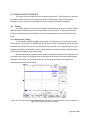
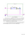
2.6. Converter Evaluation & Development Board
Usually, a development board with USB capability and some I/O capability is provided so that a
computer running LabVIEW can interface with a specific device, like the AD7280. National Instruments
sells some of these boards. For this project, we are using a board called the Converter Evaluation &
Development (CED) board developed by analog devices. “The CED1 board is part of a next generation
platform from Analog Devices Inc., intended for use in evaluation, demonstration and development of
systems using Analog Devices precision converters. It provides the necessary communications between
the converter and the PC, programming or controlling the device, transmitting or receiving data over a
USB link.” [4].
Figure 16 – Block Diagram for the CED Board. Reprinted from [4] with permission.
As shown in Figure 16, the CED board uses a 7 volt power supply and takes serial inputs and
outputs to the PC through USB. It has a Cyclone FPGA to regulate this task. We connected board
through the 96-way Connector to the Evaluation Board (EVAL board) which has 2 AD7280s in daisy chain
in series so that a PC can talk to the AD7280s.
2.7. AD7280 Evaluation Board
The EVAL board contains 2 AD7280s linked in serial daisy chain as shown on figure 2.
The master chip is connected to the 96-way edge connector which connects to the CED board as
Page 32 of 278
previously stated. This connection has CS, SCLK, SDI, SDO, CNVST, ALERT, PD and a 7 volt power
supply. All these data and control lines communicate to the SPI interface of the CED [5].
Figure 17 – Block diagram of the EVAL board. Figure reprinted from [5] with permission.
The slave device is connected to the master device in a standard daisy chain; therefore the
master can know what inputs go into slave. The master device has a 7-way connector (J2 on EVAL
Board Schematic) for cell voltage inputs and the slave device has a 6-way connecter (J3 on EVAL Board
Schematic) for cell voltage inputs. This board also supplies both these devices with thermistor inputs as
well as cell balancing circuitry [5].
The EVAL board can also be placed in a daisy chain with other EVAL boards. This is done by
turning the master chip of an EVAL board to be a slave by moving a resistor R88 to the slot R89 (from
EVAL Board Schematic) turning the board to be a slave board. Then connect the bottom 12-way
connector (J15 on EVAL Board Schematic) shown on figure 2 of the slave board to another EVAL Board‟s
top 12-way connector (J16 on EVAL Board Schematic) [5].
Additionally, the EVAL Board provides several test points that are useful for debugging purposes.
These test points are: Alert1, SDO1, SDI1, CNVST1, SCLK1, PD1, CS1, VREG1, VREF1, Alert2, SDO2,
SDI2, CNVST2, SCLK2, PD2, CS2, VREG2, and VREF2. These points can be probed with an
oscilloscope from the analog ground of the whole board. Also the way that the CED reads conversion
Page 33 of 278
data from the AD7280s is by grabbing a chunk of addresses of the AD7280s and sends that data value of
these addresses to the PC [5].
2.8. Current Mirrors
One interesting concept that will be very important to the success of the project is current mirrors.
A current mirror is an “electronic circuit that generates, at a high-impedance output node, an inflowing or
outflowing current that is a scaled replica of an input current flowing into or out of a low-impedance input
node” [34]. It is used to mimic the current in active devices regardless of voltage and loading. They are a
set of matched transistors, in this case bipolar junction transistors (BJTs), that are connected as shown in
Figure 18:
Figure 18 – NPN (left) and PNP (right) current mirrors.
The NPN mirror is said to be a “current-sinking type, because the regulating transistor [Q1]
conducts current to the load from ground” [35]. The PNP mirror is said to be in a “current sourcing
configuration, where the regulating transistor [Q2] connects the load to the positive terminal of the DC
power supply” [35]. The way that these current mirrors work is the transistors Q1 and Q4 draw current
from resistors R1 and R4, respectively. This causes a certain emitter-base voltage due to what is
essentially a diode drop. Since the bases of the Q1 & Q2 and Q3 & Q4 are connected, and assuming the
transistor pairs are matched, the same emitter-base voltage will appear at the output transistors Q2 and
Q3. This means the same current flows in I2 and I3 as flows in I1 and I4, respectively. This current is
ideally independent of the voltage across the input resistors, R1 and R4 because the base-emitter
voltages of the transistors is largely unaffected by these voltages [36]. This behavior for the NPN current
mirror, and similarly for the PNP current mirror can be derived in the following way:
The current I1 can be found using Ohm's Law: I1 = (Vb – Vbe)/R. Using Kirchhoff's
Current Law at the collector of Q1: I1 = Ic1 + Ib1 + Ib2. It is given from the diagram that the base-emitter
Page 34 of 278
voltage for both Q1 and Q2 are the same so it can be said that I1 = (β +2)Ib2, where β is the transistor
gain, which is equal in Q1 and Q2 because they are matched. It can also be said that Ic2 = β * Ib2 =
(β)*I1/(βf + 2) = Ir1/{1 + (2/β)} because of the same base-emitter voltages. Since β is assumed to be
much greater then 2, as it should approach infinity, the conclusion can be drawn that Ic2 = I1, which is the
same as I1 = 12 [37]. This would hold in an ideal case but in reality the currents are not the same. They
are, however, nearly the same.
The current mirrors will be used to convert the series implementation of the AD7280
evaluation boards to a parallel configuration. One of each of the NPN and PNP current mirrors will be
used for each of the seven data lines. The configuration of these current mirror pairs is shown in Figure
19.
Figure 19 – Current mirror pair.
As Figure 19 shows, the current mirrors operate outside of ground and Vdd. This is because the
collector voltage must be higher the emitter voltage for the NPN current mirror for current to flow, and
vice-versa for the PNP current mirror. Using the same logic as stated previously, it can be similarly
derived that the current that is seen at the up_send node will also be seen at the up_receive node. This
is the key to our projects goal of changing the series configuration of the AD7280 evaluation boards to a
parallel configuration as the current mirror scheme does not require sequential evaluation boards to
operate at different voltages.
2.9. Chapter Summary
In this chapter we have presented the fundamental building blocks which are used in our project.
Li-ion batteries are obviously the critical input of our project, although we simulate them for the
Page 35 of 278
demonstration board. This simulation is critical, because a demonstration cannot be allowed to last for
the duration of multiple charge/discharge cycles of a li-ion battery.
Page 36 of 278
3. Project Planning
To determine the best approach for completing all of the project requirements with respect to both
the product itself and the report, much thought was put into prioritizing and logistics. As with most group
efforts, it was decided that several components of the final product should be developed simultaneously.
The Gantt chart shown in Figure 20 illustrates the different components of the project and the relative
timing of their execution.
The Gantt charts shows there were four main phases of the project in addition to the final report.
The four phases were research, design, test and implementation, and integration. At times these phases
did overlap, which was necessary to further understanding of the concepts. These phases were further
broken down into two divisions, hardware and software. The hardware included designing, testing, and
implementing the current mirror circuit, designing the PCB for the demonstration board, and designing
and testing the driver board. Each of these needed to be individually tested, verified, and scrutinized as
the components were inserted into the system. The software included learning, developing, and
implementing software in LabVIEW. This also included designing the GUI. This component was
continuously developed throughout the project to accommodate further advances in hardware.
The Gantt chart above shows many components of the project were executed in parallel. Each
component had a person assigned to the task. In some cases, however, more then one person was
assigned a task due to the specialties that were involved in completing the task. Both the hardware and
software portions could be developed simultaneously as one did not always rely on the other. At certain
points during the project, integration of hardware and software had to be done to continue progress. An
example of this is testing the integration of the current mirrors into the system to troubleshoot the concept.
This was required to complete the demonstration board design.
Using these planning strategies, the group was able to complete tasks in the most efficient manner.
Additionally, assigning responsibility to each task allowed for effective communication of goals and
accountability. The parallel structure of completing tasks lead to productive use of time, and a successful
team effort.
Page 37 of 278
Figure 20 – Gant chart showing the progress of our project over time
Page 38 of 278
4. System Specifications
This section is devoted to detailing a broad overview of our project in terms of both hardware and
software. We first present a top-level description of what is happening, and then break each major
system into smaller, more detailed, components.
4.1. Overview
With the end goal of having this project provide a demonstration board (DEMO board) for use by
both the marketing department of ADI at a trade show, and the engineering departments of potential
customers, we first need to define what is going to be of use to each of these groups. For instance, when
taking the DEMO board to trade shows, there is a need for low voltages to promote safety in an
uncontrolled environment. However, when testing the AD7280, engineering groups need the full voltage
range that is required in the real application. As a result, the boards need to be able reconfigurable to
achieve either goal. The engineering teams also have a higher number of required AD7280s than the
marketing teams would, so smaller boards need to be built with the option of connecting them together.
The reason the marketing department needs the lower chip count is to be able to effectively get their point
across with as little information as possible. This is made easier if there are fewer data points to examine.
This does not help the engineering department, though, because they need to test the setup as it is
intended to be used in the real world. One final distinction between the two departments is how the data
should be presented. The marketing department requires an effective GUI, as explained previously, but
the engineering team is going to need to store the data in numeric form. We therefore needed to develop
both of these methods in the software. These results are summarized in Table 4.
Table 4 – Listing of requirements for ADI and potential customers.
ADI Marketing Dept
Safety (low voltage)
Customer Engineering Dept
Conclusion
Realistic product representation
Reconfigurable board
(full voltage range)
necessary
10 chips
20+ chips
Effective/attractive GUI
Good data acquisition
Ability to link multiple copies of
the board together
Selectable graphical or
spreadsheet output
To aid in giving the reader an understanding of how the boards we‟re developing are intended to
be used, refer to Figure 21. Figure 21 shows that we have a computer controlling a Converter Evaluation
& Development (CED) board, which communicates with the primary DEMO board. The DEMO board
may or may not be connected with additional DEMO boards during the engineering process. This last
DEMO board in the chain is driven by the driver board.
Page 39 of 278
Figure 21 – System-level block diagram of the project.
4.2. System-Level Inputs
The AD7280 is intended to measure both battery voltages and temperatures. The voltages are
taken differentially across each battery the chip is monitoring. The temperatures are typically monitored
using a voltage divider circuit where one of the resistors is a thermistor located very close to the battery,
as explained in Section 2.2. For our purposes, we have simulated batteries coming from the driver board.
To simulate the battery temperatures, we have thermistors mounted so that a cup of hot coffee can be
placed on top of them, causing the ambient temperature to rise, thus lowering their resistance, and
changing the voltage input to the AD7280.
Most of the inputs to the DEMO boards are battery voltages. When the ADI marketing
department is demonstrating the AD7280s, these inputs are going to be simulated by the driver board.
Customers will have to create their own boards to provide inputs to the DEMO board. The driver board‟s
schematic can be seen in Section 9.3. It can be seen that the driver board connects to the DEMO board
through the use of a 64-pin DIN-41612 connector. Note that many of the outputs from the driver board
are electrically identical, and provide a constant DC voltage to the majority of the inputs on the DEMO
board. In fact, on the DEMO board there are only two chips which receive a varying voltage. The voltage
on these chips can be varied by turning potentiometers located on the case of the driver board. The
rationale for this is that the customer wants to be able to see that identical inputs result in identical
outputs (thus, we have eight chips with the same inputs), but they also want to see that the chips respond
to changing voltages appropriately. When the customer‟s engineering department uses the DEMO board,
they will be applying different voltages to each input.
There is one special output from the driver board. This input is used to send a small voltage to a
current monitoring chip, the AD8210. The AD8210 is not a major part of our project, but we were
requested to include it on our DEMO board so that we could demonstrate it‟s capabilities in addition to the
AD7280. The AD8210 works by placing a shunt resistor in series with the load. Normally, the expected
load is inductive, such as an electric motor. For our simulations, however, we‟ve placed a variable
Page 40 of 278
resistance in series with the shunt resistance. The voltage is sensed by the AD8210, which then reports
a voltage output on a scale of 0-5V. Because we needed a way to communicate the voltage output to the
computer for display, we have replaced one of the temperature measurement inputs of the AD7280 with
the AD8210 output. Luckily for our project, the output from the AD8210 is on the same voltage range (0
to 5V) as the input to the AD7280 thermistor measurement.
4.3. System-Level Outputs
Our project has several subsystems. We consider each EVAL board equivalent (two AD7280s
and a set of current mirrors), the driver board, the CED board, and the GUI to be a subsystem. Each of
these subsystems communicates with the others, but the actual outputs from the system are fairly simple.
For the purposes of our demonstration, the only outputs are LED indicators and the laptop monitor. The
LEDs indicate alarm conditions, as well as cell balancing outputs from the AD7280. The laptop monitor
provides more detailed information, such as exactly what voltage each input to the AD7280s is currently
reading, the temperature at the thermistors, and a software alert flag.
Driver Board
Demo Board
CED Board
Laptop running
GUI
Figure 22- System Level Diagram
4.3.1. Driver Board Outputs
On the driver board there are three resistor networks, each of which outputs to the DEMO board.
The first resistor network provides twelve constant voltages, linearly increasing from GND to +45V. The
second resistor network also provides twelve voltages, but these are adjustable by making use of the
potentiometers on the box of the driver board. The final resistor network has one output voltage which is
sent to the current sensing chip on the DEMO board.
4.3.2. DEMO Board Outputs
The DEMO Board has five sets of two AD7280s operating in parallel. The devices communicate
with each other by means of current mirror circuits placed between the higher-potential chip of one set
and the lower-potential chip of the other set. As shown on Figure 23, this board provides outputs in the
form of an Alert LED, Cell Balancing circuitry, and Serial Communication.
Page 41 of 278
Five sets of two
AD7280s
(ten devices total)
Alert LED
Cell Balancing
Transistors and
LEDs
Current Sensing
AD8210 Chip
Serial I/O
Figure 23 – DEMO Board Block Diagram
4.3.3. CED Board Outputs
As shown on Figure 24, the CED Board has a Cyclone FPGA on it that acts as a translator
between the AD7280s and the USB port on the laptop.
Serial I/O
Data
Cyclone FPGA
Data
USB I/O
Figure 24 – CED Board Block Diagram
4.3.4. Laptop Running GUI
The laptop communicates with the CED using its integrated USB I/O port. Based on the data that
comes from the CED board, the laptop will display voltage and temperature readings from the AD7280s,
the alert LED, and the current reading from the current sense chip. The laptop also has the ability to write
to and read from the AD7280 control registers.
AD7280
Voltage
Readings
AD7280
Temperature
Readings
USB I/O
Laptop
AD7280
Control
Register Write/
Read
Alert Display
Current
Reading from
Current Sense
Chip
Figure 25 – System Block Diagram of GUI and Computer
Page 42 of 278
5. Design Methods
This chapter describes the thought process and preliminary steps that were taken to design the
final product. It is broken down into three sub-sections: product requirements, parts selection, and
software development. Each of these sub-sections details the thought and reasoning that went into
making each decision. They also describe the methods that were used to determine that something was
to be included in the final design.
5.1. Product Requirements
When designing the overall system and thinking of what it needed to do, a number of
requirements were determined to be important and needed to be especially considered in the design.
Our ultimate goal is to effectively demonstrate the capabilities of the AD7280 to potential ADI customers.
This means it needs to not only be fully functional, but also appealing to the eye, easy to understand, and
easy to use. These factors were broken down into two main categories: appeal and ease of use. A great
deal of focus was put on these factors when designing the product.
To make the product the most appealing as possible, several things had to be taken into
consideration. The first of these is the GUI that is used to display the product's functionality. The GUI
should be visually appealing so it catches the eye of a customer viewing the demonstration. This involves
an attractive and professional design with a color scheme and information that is easily read and
interpreted. In addition to this, the product must operate on a safe voltage potential to ensure the
customer would be safe using the product. The ability to be safely used adds to the appeal of the system.
Finally, the system needs to be visually pleasing. In order to satisfy this requirement the driver board
needs to be enclosed in a box that highlights the demonstration board and can be easily connected to.
The demonstration board should also be visually pleasing and the system should be designed to visually
display its capability in the most appealing way possible.
To add to its charm, the system should be easy to use and its operation and outputs should be
easy to read and interpret. To accomplish this, the GUI should have an intuitive display that highlights
important aspects of the demonstration. The information that is being displayed should be easily read
and interpreted. Since the board is likely to be used by customers with only a basic knowledge of the
system, it should be easy to teach someone how to use the product. This is accomplished by designing
intuitive and user friendly software. The software should be well documented and easy to understand.
Since the demonstration board does not use the AD7280s in the way they will be used in their full
application, the board should be easily reconfigurable to switch between series and parallel configurations
as needed.
These characteristics that enhance the appeal and ease of use of the system needed to be
considered when designing the system. They had to be included to accomplish the goal of effectively
demonstrating the AD7280. By defining these product requirements a concrete direction could be
determined and the system could be further developed.
Page 43 of 278
5.2. DEMO Board
The DEMO board grew as an extension of the EVAL board. The EVAL board was designed for
customers to gain an understanding of the functionality of the AD7280. The DEMO board is intended to
show that larger numbers of AD7280 chips can be used, as well as reduce the amount of off-board
interconnects that are required between sets of AD7280 chips. For instance, with one DEMO board, the
same functionality can be shown as with using five EVAL boards. With those five EVAL boards, however,
four sets of headers need to be installed, whereas one DEMO board could exhibit this functionality
without any off-board connections. The DEMO board does have the ability, however, to use headers to
connect multiple copies together, but the number of times this is required is greatly reduced. See Section
9.1 for the full schematic of the DEMO board.
Due to the fact that the DEMO board was extending the EVAL board, most of the design was
copied directly from the EVAL board. For instance, on the DEMO board, the digital logic communications
to the CED board, the digital logic power supplies, all digital/analog isolation, the first two AD7280 chips,
and the passive components associated with the first two AD7280s are exact duplicates of the EVAL
board. Each subsequent set of two AD7280s (and their associated passive components) is also a copy
of the first set. The biggest difference in schematic design is the ability to configure the sets of AD7280s
to be either in series or in parallel.
The reconfigurable nature of the AD7280s is a result of having two options during the assembly of
the board. One PCB is made for both options, but only certain components are inserted for either option.
The most prominent example of this is the current mirror section of the circuit. The components on those
pages of the schematic all have notes associated with them stating that they should only be inserted if a
series of parallel configuration is desired.
When a parallel configuration is desired, a set of seven NPN and seven PNP current mirrors are
inserted such that they act as voltage level shifters. The AD7280 is only designed to operate with each
subsequent chip receiving voltages at ever-increasing potentials. The chips communicate by sending
varying amounts of current instead of setting high or low voltages. Normally, that would be very clever,
but when the chips are in parallel, it means that they do not work properly because the voltages in
subsequent chips are lower, not higher. By using the current mirrors, we are able to allow the AD7280s
to source and sink current normally, regardless of whether they are at a higher or lower potential than the
next chip.
If, on the other hand, a series configuration is necessary, the current mirror setup is easily
bypassed by simply not inserting the current mirrors, and instead placing 0Ω resistors between the
relevant communication pins. This configuration is electrically the same as if five EVAL boards were
placed in series with one another.
5.3. Driver Board
The driver board was designed so as to easily integrate with, and supply the correct voltage
inputs to, the DEMO board. To do this, we first established a voltage range on which it would operate.
As we discuss in Section 5.4.2, we chose to power the driver board using a 48V DC power supply. This
Page 44 of 278
power supply was used to provide appropriate voltages to the 64 outputs that were needed to drive the
DEMO board. The schematic showing the driver board is shown in Section 9.3.
To begin the design of the driver board, we first decided that we would provide the inputs to the
DEMO board from three resistor networks, one constant, and two variable. The constant network has the
+45V rail as the input (the other end is grounded), and the outputs are sent to eight of the ten AD7280
chips on the DEMO board. The reason for sending the same voltages to so many chips is that we
wanted to show that the output from the AD7280 is consistent when the same input is applied.
The second output is sent to the current monitoring circuit using the AD8210. This circuit has
fewer components than the other two, consisting of only two fixed resistors and a potentiometer in series
with each other. The first fixed resistor shall be referred to as the protection resistor, and the second will
be called the sensing resistor. The sensing resistor is a relatively small shunt resistor tied to ground on
one side. The other end of the sensing resistor is where the output from the circuit is taken. The
protection resistor is a relatively large resistance, and is in place to make sure that the total resistance
stays high. We wanted to guarantee that the +3.3V regulator that was supplying the input would be able
to supply enough current, and did not want to load it down. When the pot is set to a high resistance,
relatively little voltage is dropped across the sensing resistor, and the output is low. Similarly, when the
pot is set to low resistance, the sensing resistor would have a large voltage drop across the terminals,
and a high signal is sent to the AD8210.
The outputs from the final variable resistor network are sent to the remaining two AD7280 chips.
These outputs are used to show that the AD7280s can dynamically react to input voltage changes. This
circuit is significantly more complicated than the other two. The input, first of all, to the resistor network is
not a voltage from one of the rails, but rather a pseudo-constant current. We made a constant current
source by using another current mirror, as shown in Figure 26. The off-page connector labeled “I_INPUT”
is the current input node attached to the variable resistor string.
The next step in the design was to overcome the challenge of providing sufficient current to the
VDD pins of the AD7280s without causing the voltage to sag in the resistor networks. We achieved this
goal by buffering the voltage outputs of the VDD outputs using opamps. The opamp buffers work to keep
the output stable under any load. Each resistor network had two opamps on it, one supplied with +48V
and +24V, the other supplied with +24V and GND, for the positive and negative supplies respectively.
The higher-potential opamp supplied the current to the higher-potential chip in each set of AD7280s, and
the lower-potential opamp similarly supplied the power for the lower-potential chip. The non-inverting
inputs to the opamps were guaranteed to never exceed their power supplies, and by connecting the
inverting inputs directly to the outputs, we were able to guarantee that the correct output would be applied
to the AD7280 inputs.
In order to provide the +24V rail needed for the opamps, we inserted an adjustable output voltage
regulator with a high voltage input capability. To adjust the output, we were able to use the formula
VOUT=VREF(1+R2/R1), where VREF is the voltage difference between the output and ADJ pins on the
device, R1 is the resistance between those same pins, and R2 is the resistance to GND from ADJ [38].
Page 45 of 278
Figure 26 – Current mirror input to the adjustable resistor network. The supply to the system is
+48V, which is much higher than the current mirror can accept. We bring the effective voltage down by
using two 20V zener diodes in series, and then dropping the remainder of the voltage across a resistor.
This ensures that the current going through I_INPUT is constant. Second order effects add non-idealities
that were small enough for our project that we ignored them.
Finally, the communications between sets of AD7280s in parallel need some biasing voltages
both greater than the highest input and lower then the lowest input. As a result, we supply the resistor
networks with +45V and GND, and bias the communications sections of the DEMO board with +48V and
-3.3V. Achieving the +48V and GND rails was a simple matter of connecting the DEMO board straight to
the power supply connector. We realized the +45V rail by using a 3.3V regulator which had it‟s GND pin
connected to zener diodes which biased up the voltage by approximately 42V. The -3.3V rail was made
by first using a +3.3V regulator, which had it‟s output tied to the input of a charge-pump voltage inverter.
All of these regulators together enabled us to have access to +48, +45, +24, +3.3, 0, and -3.3V anywhere
we needed them in the system.
5.4. Parts Selection
In any system such as the one we developed, many different components are required to
interoperate effectively. Here, we discuss some of the highest profile, and most important individual
components that made up the subsystems of our DEMO and driver boards. In fact, the majority of the
components that were used on the DEMO board were directly copied from the EVAL board upon which
we were expanding. The exception to this is listed in Section 5.4.1. On the other hand, the driver board
was being designed from scratch, so all components needed to be selected individually.
Page 46 of 278
5.4.1. Current Mirrors
The current mirrors that were selected were found at Farnell Electronic Component (FEC, or
alternately, Farnell) Distributor's Irish web page. They are the BCV61 and BCV62 current mirrors made
by Infineon Technologies3. See Figure 27 for a schematic of the integrated circuit (IC).
Figure 27 – Current mirror schematics for the BCV61 and BCV62, manufactured by Infineon.
The BCV61 is an NPN current mirror and the BCV62 is a PNP current mirror, they were made to
be complements of each other by the manufacturer. These particular current mirrors we chosen first
because the transistors inside are a one-to-one match, within the 30% tolerance specified . This means
the current in should be exactly the current out. In addition to the perfect matching, these current mirrors
operate in the voltage, current and temperature ranges that will be used for this project. Those ranges
are up to 30 volts across transistor T1, a collector current of 100 milliamps, and an operating temperature
of up to 150 degrees celcius. The voltage rating of 30 volts, however, proved to be a miscalculation on
our part as the distribution of voltage in our application was not as we expected. Details of this are in
Section 6.1. Though these current mirrors technically meet our demands and specifications, they did
raise some logistical concerns. They are surface mount IC's which have a footprint of about 2.9mm by
1.3 mm. This led to issues with testing as the pins were too small to fit into a solder-less bread board. To
compensate, the current mirrors needed to be soldered onto prototyping board and wires soldered to the
board. The soldering of such a small component led to some burnt out IC's but when successful, the
current mirrors were tested and they worked to within a tolerable amount of error.
5.4.2. Driver Board Components
The driver board we developed needed to be able to supply a large number of voltage outputs. In
order to have that capability, we used a commercially available voltage supply, four kinds of voltage
regulators, high current opamps, and two resistor networks. The specifics are outlined below. See
Section 9.3 for the driver board schematic.
3
See Section 9.4 for the datasheets of all parts listed in Section 5.4.
Page 47 of 278
5.4.2.1. XP Power AED36US48 Power Supply
The power supply we selected for our driver board was the AED36US48, manufactured by XP
Power. This is a 48V, 36W DC power supply that can be provided with either 50 Hz 240V, or 60 Hz 120V
AC power. The reason we selected this particular supply are because of the high voltage output and
relatively low cost of the product. The AD7280s require voltage inputs between 7.5 and 30V [3]. Our
DEMO board has two AD7280s in series, so the driver board needed to output at least 15V, and at most
60V. Given that we did not want the output voltages to be too dangerous, we selected the 48V output.
Additionally, we knew that in the worst case scenario, the ten total chips we were using on the
DEMO board would require 10mA each at the same time. Other parts of the circuit, of course, would also
be drawing power at that time as well, such as the resistor network we set up to provide voltage inputs
from the driver board. When we took all such factors into account, plus a safety factor of 25%, we
realized that the AED36US48‟s specified output of 750mA would easily fit our needs without any worries
about reaching current limits or blowing fuses.
5.4.2.2. AD817 High Current Opamp
Most of the voltage inputs to the AD7280s from the driver board were voltages across a series of
resistors on the driver board. The AD7280 chip has high impedance inputs, so this was not a problem.
The issue was that the driver board also needed to supply VDD for the chips, which can take as much as
10mA during an A/D conversion [3]. If we were to use the same scheme of taking the voltage from the
resistor chain, it would get loaded down by the low impedance, we would lose regulation, and the product
would not work as we wanted. As a result, we buffered the inputs to the VDD pins of the AD7280 using the
AD817. The AD817 is a high speed, low power, side supply range amplifier capable of outputting 50mA
[39]. The high current output was critical for this project because we had ten chips, and in a worst-case
scenario, they could draw a total of 100mA. Realistically, this will never happen because they are
designed to not all convert at the same time, but we decided to be very careful with our requirements.
Note that we used four AD817 chips on our driver board, as shown in Section 9.3. Two of the chips were
on a string of resistors that provided constant voltage outputs to eight chips. The other two AD817 chips
supplied power from a string of adjustable resistors to two AD7280 chips This resulted in a design that
never needs more than 80% of the maximum output current capability from the AD817.
5.4.2.3. TL783 Adjustable Voltage Regulator
In order to supply the AD817 opamps with the necessary +24V rail shown in Section 9.3, we used
the TL783. The TL783 Adjustable Voltage Regulator is a high voltage input, variable voltage output
regulator supplied by Texas Instruments. It is capable of accepting up to 125V between the input and ADJ
pins, and the output can be adjusted depending on the resistances between the output and ADJ pins, and
between the ADJ pin and circuit GND [38]. This was very convenient for our project, as it meant we could
fine tune the output to exactly what we wanted using a trim pot. As was discussed in Section 5.3, the
output voltage followed the equation VOUT=VIN(1+R2/R1). We kept R1 constant at 82Ω and varied R2.
5.4.2.4. ADP3338 3.3V Voltage Regulator
The inputs to the AD7280 were never going to reach +48V because we needed some voltage to
bias the current mirror circuit on. We needed approximately 3V on both the high and low ends of the
Page 48 of 278
voltage scale to do this. ADI supplies a 3.3V regulator with sufficient current capability for our needs, the
ADP3338. We were working with ADI, and so were able to get these components for free. Due to the fact
that we needed both +3V and +45V, we needed two of these chips. The first problem we had, though, is
that the ADP3338 cannot accept +48V as an input. To get around this issue, for the +45V regulator we
placed zener diodes between the GND pin and actual circuit GND. This allowed us to input the 48V
directly from the AED36US48 and achieve +45V output. In reality, the output voltage was +44V due to
the zeners we had selected, which was close enough for our purposes. In the case of the +3.3V
regulator, we put the zeners in series with the inputs to reduce the effective voltage input. Note that,
because we wanted GND on the driver board to be the same as GND on the DEMO board, we did not
use the +3.3V to GND as our biasing voltage, but instead used GND to -3.3V.
5.4.2.5. MAX660 Voltage Converter
In order to achieve the -3.3V mentioned in Section 5.4.2.4, we used the MAX660, a Monolithic
CMOS Voltage Converter. The MAX660 is capable of taking any positive voltage between +1.5 to +5.5V
and invert it to the respective negative voltage -1.5 to -5.5V [40]. On our driver board, we supplied the
MAX660 with the +3.3V output from one of the ADP3338 chips mentioned in Section 5.4.2.4 to enable an
output of -3.3V. This -3.3V was then sent to the DEMO board to be used for biasing the current mirrors
on, as described previously.
5.5. Software Development
We need to create a software that can show that many AD7280s can be placed in a Daisy Chain
and communicate with each other. This software also needs to be able to show the thermistor and
voltage inputs for all the devices that are connected. Also, this software needs to show off the ability for
the user to access the control registers of the AD7280s such as alert, power down, under voltage, over
voltage, under temperature, over temperature and cell balance. Therefore, we came up with the following
solution.
The software was written to communicate with the AD7280 evaluation boards through the CED
board and to show off the capabilities of the AD7280. The primary purpose of this software is to display
the capability of the AD7280s. For details of how this software is created, refer to Section 6.3 Software
Implementation of this report. The software can perform the following functions.
Page 49 of 278
Figure 28 – GUI Main Screen
Figure 28 shows the screen as you open the program. To Start using the program, click the
button Initialize and then click the button Autorun. The Initialize button downloads the software to the
AD7280 through the CED board. The Autorun button starts the reading of convertion data from the
AD7280s. While the program is in Autorun mode, hit Stop Board Actions shown on Figure 28 before
configuring registers, writing/reading to registers or saving data.
5.5.1. Board Selection
On the left side, there are 11 Buttons, Activate Board 1 to Activate Board 11. Clicking any of
these buttons will show the apropriate board data. For example on figure 3, when the Activate Board 2
button is clicked, a screen pops up showing the data for the devices on board 2. Each board has 2
devices, hence each tab on the Show Board screens will have 2 graphs.
5.5.2. Voltage Readings
Shown on board 2 on Figure 29 is the voltage readings for all the inputs for board 2 in form of a
plot and their coresponding numerical indicators. There are 2 devices on each board and each device
has 6 voltage inputs, therefore there are 12 numerical indicators shown in volts on this screen.
Page 50 of 278
Figure 29 – Cell Voltage Value Screen
5.5.3. Temperature Readings
Each board screen has 2 tabs, Voltage Readings and Temperature Readings. Figure 30 shows
what happens to the Show Board 2 screen when the Temperature Readings tab is clicked.
Figure 30 – Temperature Screen
After that tab is clicked the screen shows the thermistor readings in Celsius for the thermistor that
are attached to board 2.
Page 51 of 278
5.5.4. Reading from and Writing to all the AD7280 Registers
Before using this function, Stop All Board Actions should be clicked for safety measures. To use
this function, click on the button on the upper left hand corner called Write/Read Single Register and a
screen shown on Figure 31 should popup.
Figure 31 – Register Read/Write Screen
This function allows the user to read from and write to any device for up to 11 boards.
That is Device 0 to Device 22. The buttons labeled Device 0 on Figure 31 are drop down menus. Figure
32 shows what happens when the user clicks on them. The buttons on the right side are for reading and
the buttons on the left side are for writing.
Page 52 of 278
Figure 32 – How to select a device
After clicking on the drop down menu, the user can select which device to write to or read from.
The button Control High is also another dropdown menu. Figure 33 shows what happens when
that button is pressed.
Page 53 of 278
Figure 33 – How to select a register
The button indicated in Figure 33 selects a specific register that the user wants to write to or read
from.
Lastly, after a specific device is selected and a specific register is selected, clicking the Read
button shown on Figure 31 will read the value of that register on that device. The user can also use the
Device Select (W) and Register Select (W) buttons shown on Figure 33 and click on the Write button on
figure X5 to write to that specific Register on that device.
5.5.5.
Automatically Configuring the Alert Function
The AD7280 has a user-configurable alert function. The user can configure the voltage inputs
and thermistor inputs in which an alert flag is set by using the Write/Read Single Register function.
Figure 34 shows a button called Autoconfig Registers and a numeric indicator circled in red. This
button allows the user to automatically setup the alert condition with a single click. The user needs to
enter the number to devices that are being used on that numeric indicator before clicking on Autoconfig
Registers.
Page 54 of 278
Figure 34 – Button to click on to configure alert condition
Currently, this function is set in such a way that if any input cell voltage is less than 2.5 volts and
greater than 5 volts, then the alert flag gets set. This also triggers the LED, D10 on the evaluation board
indicating that the alert flag is set. Temperature conditions in which the alert flag is set is not part of this
function so the thermistor alert triggering is set to default which is alert when temperature is outside of this
range -50 degree C to 150 degree C.
Once Autoconfig Registers is pressed, a screen will show up confirming that the button has been
pressed. Press the Write button on that screen for this function to take effect.
5.5.6.
Save All Converted Data
Before pressing the button, remember to toggle Autorun and Stop Board Actions off. Pressing
the Save All Converted Data indicated in Figure 35 button will prompt you to save to a directory that you
select. It is recommended to open the saved file as an excel spreadsheet.
Page 55 of 278
Figure 35 – Button to click on to save data
The saved file has the format shown in Table 5.
Table 5 – How to read the saved data
Device
1
Device
2
…
Cell 1
Cell 2
Cell 3
Cell 4
Cell 5
Cell 6
Cell 1
Cell 2
Cell 3
Cell 4
Cell 5
Cell 6
Volt
Volt
Volt
Volt
Volt
Volt
Temp
Temp
Temp
Temp
Temp
Temp
Data
Point
1
Data
Point
1
Data
Point
1
Data
Point
1
Data
Point
1
Data
Point
1
Data
Point
1
Data
Point
1
Data
Point
1
Data
Point
1
Data
Point
1
Data
Point
1
…
Data
Point
2
Data
Point
2
Data
Point
2
Data
Point
2
Data
Point
2
Data
Point
2
Data
Point
2
Data
Point
2
Data
Point
2
Data
Point
2
Data
Point
2
Data
Point
2
…
Data
Point
3
Data
Point
3
Data
Point
3
Data
Point
3
Data
Point
3
Data
Point
3
Data
Point
3
Data
Point
3
Data
Point
3
Data
Point
3
Data
Point
3
Data
Point
3
…
…
…
…
…
…
…
…
…
…
…
…
…
…
Page 56 of 278
5.5.7.
Show 10 Chips
Figure 36 shows a display of 10 devices with their voltage inputs and their temperature readings
as well as a battery bar indicator.
Figure 36 – showing 60 cell voltage and temperature readings
5.5.8.
Selectable Detailed Display of all Devices
Figure 37 shows a screen that displays all the function of an AD7280 displaying all its control
registers, alert indicator, temperatures, and voltages. It even has a selector to select between difference
devices in the daisy chain and a current sense display that shows the current readings coming out of the
current sense chip. A special button to note is the Invert Temp Reg button. Since the thermistor readings
decrease in voltage drop as temperature goes up, the alert conditions are inverted. Pressing this button
will correct this condition by inverted all input values the user sets to the registers.
Page 57 of 278
Figure 37 – All capabilities of the AD7280 are displayed on this screen.
Page 58 of 278
6. Implementation/Results
This section covers the steps we took to make this project work. This will include how we wrote
the software, details of current mirror behavior for different configurations, steps we did to get the
AD7280s to work in series, how we designed the PCB, and how we tested each subsystem.
6.1. Testing
This section details how each block of hardware and software was prototyped. We also explain
particulars about troubleshooting and the revision history of various blocks. In cases where we were
stuck for extended periods, several different revisions were attempted until a successful solution was
found.
6.1.1. Initial Series Testing
To test the daisy chaining capability of two boards, we connected the J15 connector of a slave
EVAL board to J16 connector of a master EVAL board. We then used a configuration that we were told
that allows the software to see all four devices (two devices per board). This configuration is turning off
temperature readings this supposed to cause voltage readings from the slave board to show up in place
of the temperature readings of the master board.
We were not getting any readings for the second board despite implanting this configuration. So
we checked to see if there is a hardware issue by probing the test points to the communication signals
between the two boards. The following are pictures we took of the waveforms of the signals that
communicates between the two boards.
Figure 38 – This picture shows what happens when the Alert Test Point Is Probed. Alert can either be a
high or low, and on this picture it is a high.
Page 59 of 278
Figure 39 – This picture shows what happens when the CNVST Test Point Is Probed. CNVST is either a
high or a low, and in this picture it is a high.
Figure 40 – This picture shows what happens when the CS test point is probed. Chip Select is active low
and is pulled low periodically.
Page 60 of 278
Figure 41 – This picture shows what happens when the PD Test Point Is Probed. PD is either a high or a
low and is active high, and in this picture it is a high.
Figure 42 - This picture shows what happens when the SCLK Test Point Is Probed. During operation, the
PFGA sends bursts of clocks periodically. We see that a 1 MHz clock is being busted every
approximately. 30ms
Page 61 of 278
Figure 43 – This picture shows what happens when the SDIhi SDOlo Test Point Is Probed with 10ms time
scale with 10ms time scale. Every few 20 to 30ms, a stream of bits is sent.
Figure 44 – This picture shows what happens when the SDIlo SDOhi Test Point Is Probed with 10ms time
scale. Every few 20 to 30ms, a stream of bits is sent.
Looking at Figure 43 and Figure 44, we see that SDIhi SDOlo and SDIlo SDOhi are sending data
signals between the two boards, so the two boards are talking to each other and therefore it was not a
hardware issue. We next move to test the software.
We figured that a good starting point in figuring out what is wrong would be to see what the data
array from the VI Manual Receive from CED is reading. Figure 45 shows the values of this array.
Page 62 of 278
Figure 45 – Data array from CED with Turning off Temperature Readings to Collapse the Data Stack
We noticed on Figure 45 that starting from the column of index 48; the data repeats itself as if it
was from index 0. Also the first row of Figure 45 has a repetition of 0, 0, 128, 128, 0, 0, 128, 128, 0, 0…
The value 128 has to do with device select, and since there are 4 devices attached and there are only two
different device select values, we concluded that something in the software is not telling the CED to
upload the data from the other two devices.
Figure 46 – Data array from CED before problem fixed without with Turning off Temperature Readings to
Collapse the Data Stack
Page 63 of 278
We then turn the temperature readings back on as Kate‟s trick had not worked. We noticed that
the first row of Figure 46 showed 0, 0, 1, 2, 128, 128, 129, 130, 0, 0, 1… The values 1 and 2 are 0+1,
and 0+2 which is an offset from device select which indicates temperature readings. The same can be
said for the values 129, and 130 which is 128+1, and 128+2. We are however still seeing only two
devices being read. This confirms that the software is not telling the CED to upload the data from the
other two devices.
Next we noticed that each device holds twelve data values. For example the data values for
device one is contained in indexes 1, 3, 5, 7, 9, 11, 13, 15, 17, 19, 21, 23 from Figure 11. The data
values for device two are contained in indexes 25, 27, 29, 31, 33, 35, 37, 39, 41, 43, 45, 47 from Figure
46. That makes a total of 24. So we looked into the upload data code for any value of 24, and we saw
the value conversion results per set are set to 24. We changed this value to 48.
We tried running the code again and there have been no changes. We looked further again and
it turned out that there were 2 variables that we needed to change in order to change conversion results
as there was another value that was 24 in the start real time function that tells the CED the number of
frames it needs to grab. So we changed the number of frames to 48 and all four devices are seen by the
software.
Figure 47 – Data array from CED after problem fixed
Figure 47 shows a 3rd device select value in the data array after increasing the number of frames
that the CED grabs. Therefore, we now have the software to test the current mirrors.
Page 64 of 278
6.1.2. Current mirror verification.
After the current mirrors were soldered to a prototyping board and they were capable of being
placed into a bread board, they were tested to verify their operation. Figure 48 is the circuit that was used
to perform this test.
The resistors R1 through R4 were not always the same for the duration of the project. However,
in a single set of tests they did remain the same, R3 would always equal R4 and R1 would always equal
R2. This was needed to prove that the current flowing through the current mirror to ground was the same
on both ends with the highest efficiency. A test was performed by applying a Vdd to two of the pins of the
current mirror, pins 1 and 2 of the NPN current mirror and pins 3 and 4 of the PNP current mirror. The
voltage is applied at these pins due to the nature of NPN and PNP transistors. In both cases the other
two go through a resistor to ground. The voltage needs to be higher at the collector then the emitter for
NPN transistors and vice-versa for the PNP transistors. The voltage was measured across the two
resistors with a digital multimeter. A current mirror was proclaimed acceptable if the voltage readings
were within 10%, meaning the current flowing through the resistors were within 10% because Ohm's law
says that V=IR and in this experiment R is constant. The 10% error was deemed acceptable because in
the application of these current mirrors the values that will be used are 200 micro amps to represent a
high signal and 20 micro amps to represent a low signal. If the current mirror is off by the maximum 10%,
a high signal can still not be misinterpreted as a low because the cutoff between high and low is close to
100 micro amps. An example of a test done on a pair of current mirrors, one NPN and one PNP, and
using the symbols from above, is the following: Vdd = 5V, R1 = R2 = R3 = R4 = 5kΩ. The voltage
measured across R3 and R4 was 4.463V and 4.465V, respectively. This is a good current mirror and the
error is less the a tenth of one percent. The voltage measured across R1 and R2 was 4.457 and 4.624,
respectively. This current mirror is also good as it is only off by 3.61 percent. Each of the current mirrors
used was tested in this manner to verify good operation before it was placed into a more advanced circuit.
Figure 48 – NPN (left) and PNP (right) current mirror test circuits
Page 65 of 278
After it was certain the current mirrors were working properly, a circuit had to be designed to use
them as a level shifter that can draw and supply the same current from the 45-volt level to the 3-volt level.
The 45V and 3V are relative to earth round and are used as Vdd and GND, respectively. The first circuit
that was tested for this purpose is shown in Figure 49:
Figure 49 – First full current mirror experiment
This test was done with Vdd = 10, R1 = R5 = 22kΩ, and R2 = R3 = R4 = 1.5kΩ. A successful
experiment would result in the voltages across R2, R3 and R4 all being the same. This would show that
the current flowing through the input ad output parts of the circuit are the same. The voltages were
measured across R2, R3 and R4 and were 0.008V, 0.006V, and 0.134V, respectively. These values are
not within the allowable amount of error. Additionally, they are not consistent with the higher voltages that
were expected in this experiment. It was fount that most of the voltage was dropped across R5, 9.30V. A
second experiment was done on this circuit with the resistors changed. They were changed to R1 = R5 =
5kΩ, and R2 = R3 = R4 = 1kΩ. The experiment had the same goal as the previous one and, similarly,
was not a success. The voltages measured across R2, R3 and R4 were 1.23V, 0.204V, and 1.392V,
respectively. These voltages are not a successful result. Most of the voltage in this case was dropped
across R1, with 7.97V. These experiments did not work because the voltage at the collectors of the
transistors was not regulated, meaning neither was the current, and the resistor R3 was connected to the
wrong pin. The voltage at the collectors needed to be regulated and R3 needed to be connected from pin
1 to Vdd.
The next experiment that was done had the resistors in the correct place but was still not the
correct circuit. The schematic of the circuit is shown in Figure 50.
This test was done with Vdd = 5V and R1 = R2 = R3 = R4 = 5kΩ. In a successful experiment the
voltages across R2 and R3 would be the same. Vdd was applied and the voltages across all of the
Page 66 of 278
resistors were measured with a digital multimeter. The voltges were found to be 3.071V, 1.414V, 1.609V,
and 3.272 across R1, R2, R3, and R4, respectively. This means the percent error between the currents
going through R2 and R3 is 12.1% which immediately makes the test unsuccessful. A few minor changes
were made to the circuit to further the understanding of the concepts. First, all of the resistors were
changed to 1kΩ. In this case, the voltages across R1, R2, R3, and R4 were found to be 3.065V, 1.379V,
1.587V, and 3.273V, respectively. This resulted in a higher error of 13.1% relative to the error of 12.1%
found in the previous experiment. This shows that the decrease in resistance resulted in a higher error.
Additionally, it showed that the voltages across R1 and R4 remained very close to the same, meaning the
voltage at the collectors of the transistors was close to the same in both experiments. The next change
that was made to the experiment in Figure 50 was Vdd was changed to 10V and the -5V supply was
changed to -10V. This resulted in readings of 6.76V, 2.575V, 2.856V, and 7.04V across R1, R2, R3, and
R4, respectively. The error between the currents was 9.8%. This would seem be a good experiment but
the increase in voltage spread across the whole circuit is the reason it appeared to be a success. Taking
the readings from R1 and R4, it was revealed that the error in those readings was 4.0%. In the first two
experiments the error in these voltage readings was 6.1% and 6.4%, respectively. It appears that the
reduction in error between the voltages at the collectors of the transistors is what reduced the error in the
voltage readings across the resistors R2 and R3. This means that the voltages across R1 and R4 should
be the same in the circuit for the current mirrors to work as desired which suggests regulating the voltage
at the collectors of the transistors.
Figure 50 – Second full current mirror experiment
The next test that was attempted includes two additional transistors that are used for their
diode drop properties. This will regulate the voltages at the collectors of the transistors to the fixed value
of a diode drop. The schematic of this circuit is shown in Figure 51.
Page 67 of 278
This test was done with Vdd = 5, R1 = R2 = 1kΩ, and R3 = R4 = 660kΩ using a resistance of two
330kΩ resistors in series. The resistances were measured with a digital multimeter and found to be
closer to 664kΩ. Such a high resistance was used to simulate a high impedance input and output that the
application of this current mirror circuit will use. The two transistors Q5 and Q6 act as diodes and
therefore drop a diode voltage. This means that the collectors of the PNP current mirror transistors are at
a diode drop above Vdd and the collectors of the NPN current mirror transistors are at a diode drop below
ground. A successful experiment would result in the voltages across R3 and R4 being the same. The
voltage across the the resistors R1,R2, R3 and R4 were measured and were 4.325V, 4.235V, 5.250V,
and 5.663V, respectively. The percent error between R3 and R4 was 7.3%. To verify the successful
operation of this circuit, the 664kΩ resistors were replaced with 330kΩ resistors. The voltages were
measured and found to be 5.247V across R3 and 5.668 across R4, off by only 7.4%. This is determined
to be a successful experiment. As a result, our current mirror circuit block was modeled after this circuit.
A point of significance is the voltages across R1 and R2 were off by only 2.1%. This is the reason for the
smaller error of 7.3% between the voltage measurements across R3 and R4. The diode drops across the
transistors Q5 and Q6 are the closest relative to each other that can logistically be obtained so this is how
it will be done in the final applications.
Figure 51 – Third full current mirror experiment.
After determining a current mirror circuit that would operate as desired, a fixture of seven of these
circuits had to be built. Seven because there are seven data lines going from one set of AD7280s in
parallel to the next set. Of these seven data lines, five of them are up sends, meaning the data is sent
from the master to one of the slave boards. The other two data lines are down sends, meaning the data
is sent from one of the slave boards to the master. The schematic for the first circuit that was designed
and soldered to prototyping board is shown in Figure 52.
Page 68 of 278
Figure 52 – First current mirror circuit using all seven data lines.
This circuit shown in Figure 52 uses the diode-drop transistors and pins 3 and 4, the collectors,
are all connected to the corresponding diode-drop transistor. This regulates the voltage at the collectors
of the transistors as explained previously. This circuit was tested using down send and up receive
terminated at Vdd and down receive and up send terminated at ground. The Vdd that was used was 5V
and the terminating resistors in both cases were 664kΩ. The complete results of this experiment can be
seen in Table 6. This circuit was tested successfully as each of the current mirror pairs yielded an error of
less then 10%, in fact, the average error was only 3.67%. However, before this circuit was attempted in
the parallel configuration, it was realized that there was a problem. The connections of all of the pins 1
and 2 for all of the current mirrors needed to be switched. This is because in our application the send
signal must be the one that is directly connected to the bases of the transistors in the current mirrors.
This ensures that the current in a current mirror is the current out as both of the base currents are the
same. The reason it worked in the test is because the resistors were a passive load so there was no
defined send signal and receive signal. In the application the load will be active so the send signal must
be connected to the transistor bases.
Table 6 – Results of the experiment shown in Figure 52
A second current mirror circuit was designed and soldered on to prototyping board. The circuit is
the same as Figure 52 except each of the pins 1 and 2 of the current mirrors are switched. This new
circuit schematic is shown in Figure 53.
Figure 53 – Second current mirror circuit using all seven data lines. Send signal connected to the base of the receiving current mirror transistor
The circuit in Figure 53 was fabricated and tested. It was tested in the same way as previous,
with VDD = 5V and the down send and up receive terminated at VDD and down receive and up send
terminated at ground, each through 664kΩ resistors. For the complete results of this experiment, see
Table 7. This board was tested successfully as all of the readings were off by less the 10%. The average
error was 5.9% which is slightly higher than the average error in the previous circuit but still well within
specifications. Since the send signal is connected to the transistor bases, as stated previously, this is the
circuit that will be inserted into the parallel configuration
Table 7 – Results of the experiment shown in Figure 53.
6.1.3. Initial Parallel Testing
After finding a current mirror circuit that will work as desired and designing the software to be
capable of handling the new parallel configuration, the current mirror circuit was inserted into the system.
The seven data lines from the master board were connected to the PNP current mirrors and the seven
data lines from the slave board were connected to the NPN current mirrors. Figure 54 is a block diagram
of the parallel test configuration:
There is one current mirror pair for each of the seven data lines. The arrows in Figure 54 show
the flow of current going from the slave towards the master. According to the test data that was obtained
in the individual tests, this circuit will output a current that has better than 10% error compared with its
input. The power rails were set up using two dual rail power supplies, allowing for four different voltage
levels and a ground. The power rails were 0V, 3V, 23V, 43V, and 46V. The symbolic representations of
those voltages are GND-3, GND, VDD/2, VDD, and VDD+3. A block diagram of the circuit is the shown in
Figure 55.
Initially when the voltage was applied to this system the current limit indicator on the power
supplies would activate. This would seem to mean there is a short somewhere in the circuit. Because of
this, the circuit was rewired several times in an attempt to eliminate the short circuit. At one point in the
rewiring a short was actually created and the AD7280s on the slave evaluation board were destroyed. At
this point new AD7280s were obtained and professionally mounted to the evaluation board. The new
board was tested and it was confirmed to function properly on its own. With the new board in and the
system verified to be wired correctly, the current limit indicator on the power supplies still activated when
the voltage was applied. The current limit was set to 20mA for the entire system. When the limit was
relaxed to 22mA the indicator would flicker on and off. This would seem to mean that 22mA is close to
how much current the system actually draws. The limit was then relaxed to 30mA and the indicator did
not go on after that point. The current drawn by the entire system was about 22mA at the given voltage,
as indicated by the power supply reading. There was no short.
Figure 54 – Test integration of current mirrors.
When the voltage was applied to the system at the levels previously indicated and there were no
setbacks, an attempt was made to download the code to the board and attempt to read data. The
software showed that the first board was reading data but the second board, connected through the
current mirrors, was not.
This contrasted the results from the series test where both boards and all four AD7280s would
read data correctly. This means that the error must be related to the current mirrors being introduced into
the system. An analysis of the data line SCLK was done due to the nature of a clock signal being a
periodic square wave that is easily identifiable. Probing was done with an oscilloscope through a diode
on the send signal, a test point on the receive signal, and through a resistor in between the current
mirrors.
Page 73 of 278
Figure 55 – Block diagram of the parallel test setup.
The diode that was probed to obtain an SCLKhi signal on oscilloscope s D15. This is because
the oscilloscope can only read voltage so the wire itself can not be used as a test point, there must be an
impedance. At the master board J16, pin 5, which is SCLKhi, the signal seen on the oscilloscope can be
seen in Figure 57.
Page 74 of 278
Figure 56 – Data from the master board (top) and the slave board (bottom). Note that the slave is not
receiving data.
Page 75 of 278
Figure 57 – Signal of SCLK from Test Point on Master Board
Figure 57 is a healthy looking clock signal meaning the problem with the system does not lie in
the master board send signal. Next, the bridge wire between the NPN and PNP current mirror was
probed with an oscilloscope through a resistor. Figure 58 shows the location that was probed to obtain
the signal:
Figure 58 – Probe of SCLK signal after one current mirror
The obtained signal should be the same as the signal that was sent from the master board
because the current in the current mirror circuit should be the same throughout.
Page 76 of 278
The signal displayed in the output of the first current mirror is not what was expected as a signal
similar to Figure 57 should have been what was seen. The obtained signal just looks like noise. This
result means either the signal has been corrupted after coming through the first current mirror or the
probe location is invalid. Since the signal is being measured from a resistor it is known the signal
obtained should be a scaled version of what was seen at the master board meaning the probe location is
valid. A probe after the second current mirror was done to verify the result. The SCLK signal was
measured at the test point on pin 5 of J15, the input to the slave board.
The probe was placed on the SCLK test point on the PCB. The received signal should a scaled
version of Figure 57. This data line was probed at the test point shows the signal coming from the
second current mirror.
The signal coming from the second current mirror does not look like the signal that was seen at
the output of the master board or the signal that was seen between the two current mirrors, but rather a
signal that is nothing much more then ambient noise. After seeing these results of the AC analysis of the
current mirror circuit, a new approach had to be devised to gain a better understanding of the system.
The main concern was the current mirror data sheets specified the use of both AC and DC current
mirroring but the tests to verify the current mirror operation were all done using DC supplies. There was
no initial test done to verify operation using AC supplies which is what is used in the application of the
current mirrors. Further investigation needed to be done.
We looked closer into the current mirror data sheet and noticed that the current mirrors can only
operate up to 30 volts across the transistor at pins 2 and 3. The voltage across them in the full test that
was done with all seven data lines was close to 44 volts on the sending current mirror. This voltage is
well out of specification and is the reason that the current mirror circuit did not perform as expected in the
test.
A new current mirror circuit was built because the previous one had been destroyed due to the
over-voltage. The circuit was tested with the DC analysis as before and passed with similar results. The
voltage across the system was setup lowered to 26 volts with the rails on the power supplied set at 0V,
3V, 13V, 23V, and 26V that are represented by GND-3, GND, Vdd/2, Vdd, and Vdd+3, respectively.
Again, the SCLK was chosen for AC analysis because of its predictability. The same locations as the
previous test were probed. The signal measured from the master board at pin 5 on J16 is shown in
Figure 59.
As before, Figure 59 shows a healthy clock signal. The goal is for the rest of the probe locations
to result in the same display. The next probe was taken off of a resistor between the two current mirrors.
Figure 60 shows the display of the oscilloscope.
Page 77 of 278
Figure 59 – Picture of SCLK test point output from the Master Board
Figure 60 – Signal of SCLK Signal after One Current Mirror
This signal is what was expected and desired. It is a bit attenuated but that is also expected
because the oscilloscope reads voltage and the output is a current. The oscilloscope cannot account for
the difference in impedance between the diode probe and resistor probe so a scaled version is
acceptable. Since this signal is good, it should also be what is seen at the output of the second current
mirror. Figure 61 shows the reading from the test point on pin 5 of J15 on the slave board, which is the
Page 78 of 278
signal after going through the current mirror circuit, as well as the diode on pin 5 of J16 on the master
which is the signal that is sent to the input of the current mirror:
Figure 61 – SCLK from the slave board
Note the difference in scale of the oscilloscope in this figure versus the previous figures. This is a
good signal. Also not the attenuation of the signal received by the slave board. This is, again, a result of
different impedances on the test points which is acceptable. The figure shows that the output of SCLK
from the master is very similar to the input of SCLK to the slave coming from the current mirrors. This is
when it was realized that the current mirrors being used before had been destroyed due to their being
used out of specification.
We then tested the four additional current mirror pairs in the up send configuration using the
SCLK signal. This is because the master device has five send pins, which send data from low potential to
high potential, and 2 receive pins which receive signals from a higher potential to a lower potential. The
five send signals worked as desired as results similar to the previous experiment were seen from each
current mirror pair. The same test could not be done on the two receive pins because it is not known
what signal to expect when only one of them are connected in the system. Instead, the whole current
mirror circuit was connected after verifying the voltage on the power supplies were low enough to safely
operate the current mirrors. The devices were connected and an attempt to read data was made. At the
low voltage and using the thoroughly tested current mirror circuit, data was successfully read from both
the master board and slave board in the parallel configuration for the first time.
6.1.4. EVAL Board Final Testing
During the testing of the system in parallel with the current mirrors, the received signal through
the current mirrors would break down at a certain voltage rendering is useless. This voltage at which the
received signal breaks down is 20.5V across pins 2 and 3 on the PNP current mirrors in the up send
Page 79 of 278
signals and across the NPN current mirrors in the down send signals. That is not consistent with the
absolute maximum voltage of 30V allowable by the current mirrors according to the data sheet. This can
be attributed to the fact that very small signals, 200 micro amps for a high, are being used and the 30V
rating is an absolute maximum meaning operation at that voltage is unstable. This breaking down of
signals can be seen on all data lines. The first test of this was on the data line SCLK which is an up send
signal, from master to slave. A healthy SCLK signal would look Figure 62.
Figure 62 – Healthy SCLK Signal
This is the signal that was sent and measured from the master board through a diode at pin 5 of
J16 regardless of the voltage put across the system. It is also the signal received at the pin 5 of J15 test
point on the slave board before the voltage across pins 2 and 3 of the PNP current mirrors reaches
20.5V. When the voltage across the entire system rose above 26V, the voltage across pins 2 and 3 of
the current mirror reached 20.5V. At that point the SCLK signal received by the slave board at pin 5 of
J15 looked like Figure 63.
Figure 63 shows that there is a limit to the voltage that can be across the system. After this limit
the SCLK signal is corrupted which means the rest of the system cannot function properly. To verify, the
SDOlo signal was measured at pin 8 on the J15 test point on the slave board. When the voltage across
the system is low enough and the SCLK signal is functioning properly, The SDOlo signal looks like Figure
Figure 64.
Figure 64 shows a down send signal data line, meaning that the data flows from slave to master.
Down send signals measured at the slave should look like the above signal unless there is some kind of
corruption in the entire system. Knowing this, and the point at which SCLK becomes corrupted, the signal
Page 80 of 278
was measured again with a voltage across the system known to corrupt SCLK. The signal obtained is
seen in Figure 65.
Figure 63 – Corrupted SCLK signal
The figure shows that the SDOlo signal has been corrupted by the high voltage and therefore the
entire system data communication becomes corrupted when the voltage rises above 26V across the
system. This also explains the failure of the first test. The first test was done at a voltage of 48V across
the system. Not only is this much higher than the 26V at which the data signals become corrupted, it
would also result in a voltage of about 44V across pins 2 and 3 of the current mirror which is 14V more
across the transistor then the absolute maximum according to the data sheet.
Figure 64 – Healthy SDOlo Signal
Page 81 of 278
Figure 65 – Corrupted SDOlo Signal
The voltage across the system in our application needs to be 51V which, if not compensated for,
will result in the same failure as the first test on the current mirrors where the absolute maximum rating is
surpassed and the signals were corrupted. To solve this problem a zener diode was placed in between
the two current mirrors. The schematic of a single current mirror is shown in Figure 66.
The zener diode that was used in the test was 20V. This value means the first 20V across the
system has to be dedicated to the zener diode but the system would be able to operate at a higher
voltage then it was previously able to. When the 20V zener diode was inserted, a test was performed on
SCLK to find out at what voltage the signal breaks down. The break down voltage was found to be 42V.
This is a better result as it is now known that the zener diode increases the amount of voltage that the
system can handle. There is, however, now a higher minimum voltage that can be put across the system.
This voltage is 26V, giving a 16-volt resolution. If the system was given a voltage under 26V there would
be no reading by the software because it would be below the threshold. The 16V resolution is still an
improvement over the circuit with no zener diode, however. The resolution in that case was 5 volts as
each AD7280 needs at least 7.5V to operate and the current mirrors operate 3 volts out of ground and
Vdd meaning the system could only operate between the voltages of 21V and 26V. In the application of
this system the zener diode will need to be higher than 20V to be able to raise the total voltage across the
system to 51V but the tests show that the concept of inserting a zener diode works.
Page 82 of 278
Figure 66 – Schematic of current mirror with zener.
6.2. Software Implementation
This software is based on Kate O‟Riodan‟s AD7280 Evaluation Software. Some of her code is
left here for debugging purposes, however if this document does not mention it, the programmer should
just ignore it because it‟s not used. Her software was designed for two AD7280s on one EVAL Board and
there were some issues involving memory refresh. The CED buffer is directly linked to the memory of the
Cyclone FPGA. Some of the changes from Kate‟s software include the characteristic in which this
software refreshes the CED buffer every 10 seconds so that it can run indefinitely, allowing for register
access for 22 devices, a popup board screen to see conversion data for 22 devices, and an auto
configuring of alert settings. The idea behind this software is to communicate through USB with the CED
board as the CED board reports data from the AD7280s.
The AD7280 DEMO Software uses a button triggered interrupt type of actions. What this means
is, whenever a button is pressed, a variable is set and depending on the numeric value of that variable a
specific action is performed.
For example, for the Read/Write Single Register button is pressed then the Read/Write Single
Register variable is triggered to a value of “true” and that activates a block of code is run shown on Figure
67. All this block of code does is to set a value 4 to the variable num.
Page 83 of 278
Figure 67 – Read/Write Single Register triggering
This software is also hierarchical based, which means that there is a VI called AD7280main.VI
that is always running and it calls on other VIs during its operation as shown on Figure 68. These VIs
when called can do anything from modifying the AD7280 registers to displaying conversion data. The VIs
on lowest level are used for FPGA communication through the USB to the CED board. These VIs are
shown in green and blue and they are Configure Power Supplies, Program Board, Search for Boards,
Manual Receive From, and Manual Send to. All other VI, the ones shown in blue and white are higher
level VI that takes the data from the FPGA VI and does parsing and plotting with it. Parsing is extracting
required data from information returned from a lower level VI that is not in a useful form. For example, if a
lower level VI returns a stream of bits, another function is required to break down the stream of bits and
acquire useful information from just a stream of bits. Plotting is displaying the information on a chart.
Figure 68 - VI Hierarchy
6.2.1. Examining the Lower Level Code
The following is documentation of how the button pressing relates to certain actions being
triggered as well as what the code does as it runs continuously. As stated before, this software has a
main VI always running in the background and events get triggered based on the user pressing certain
buttons causing interrupts.
Page 84 of 278
6.2.1.1. Event Triggering
There are a few event triggering variables, namely Numeric 5, and num.
num has the highest level of control for it controls how the program behaves.
Figure 69 - num triggering
If num = 0, a function is triggered to initialize the AD7280s through the CED.
If num = 1, a function is triggered to download the code to the AD7280s through the CED.
If num = 2, a function is triggered to upload the conversion data continuously from the AD7280s.
If num = 3, a function is triggered to stop the program from running.
If num = 4, a function is triggered to allow the user to write/read all critical AD7280 registers.
If num = 5, a function is triggered to automatically configure the alert settings AD7280 registers by
auto-writing to certain registers.
Numeric 5 governs which DEMO-board is active.
Figure 70 - Numeric 5 Triggering
If Numeric 5 = 0, all functions from devices on all the boards are stopped.
If Numeric 5 = 1, a function is triggered to upload data from the devices on Board 1 and a screen
pops up showing all the data from Board 1.
If Numeric 5 = 2, a function is triggered to upload data from the devices on Board 2 and a screen
pops up showing all the data from Board 2.
If Numeric 5 = 3, a function is triggered to upload data from the devices on Board 3 and a screen
pops up showing all the data from Board 3.
Page 85 of 278
If Numeric 5 = 4, a function is triggered to upload data from the devices on Board 4 and a screen
pops up showing all the data from Board 4.
If Numeric 5 = 5, a function is triggered to upload data from the devices on Board 5 and a screen
pops up showing all the data from Board 5.
If Numeric 5 = 6, a function is triggered to upload data from the devices on Board 6 and a screen
pops up showing all the data from Board 6.
If Numeric 5 = 7, a function is triggered to upload data from the devices on Board 7 and a screen
pops up showing all the data from Board 7.
If Numeric 5 = 8, a function is triggered to upload data from the devices on Board 8 and a screen
pops up showing all the data from Board 8.
If Numeric 5 = 9, a function is triggered to upload data from the devices on Board 9 and a screen
pops up showing all the data from Board 9.
If Numeric 5 = 10, a function is triggered to upload data from the devices on Board 10 and a
screen pops up showing all the data from Board 10.
If Numeric 5 = 11, a function is triggered to upload data from the devices on Board 10 and a
screen pops up showing all the data from Board 11.
6.2.1.2. Button Triggering Event
The way to trigger these numeric variables is by the use of buttons as discussed in the
previous section. These seventeen buttons are Autorun, Auto Config Registers, Write/Read Single
Register, Initialize, Stop Board Actions, and Activate Board 1 to Activate Board 11. The buttons can be
seen as boolean variables, and when they are pressed they are true and when they are unselected, they
are falese.
When Autorun is true as shown on figure 20 the variable, Numeric 4 is incremented until
Numeric 4 = 500. If Numeric 4 = 500 then Numeric 4 is set to 0. If Numeric 4 is less than 498 then num
is set to 2, which triggers a function to upload the conversion data continuously from the AD7280s. If
Numeric 4 is less than 500 and is greater than 498, num is set to 1 which triggers a function to redownload the code to the AD7280s through the CED.
Page 86 of 278
Figure 71 - Autorun Triggering
The reason for this to toggling is if the CED continuously upload data then it will the CED buffer
will be full thus causing the device to stop working. Therefore, re-downloading the code once in a while
will clear up the buffer. Another reason for setting num = 1 periodically is to ensure that the CED is ready
to upload data after each refresh.
If Initialize is true, then num is set to 0 as shown on Figure 61.
Figure 72 - Initialize Triggering
If Autoconfig Registers is true then num is set to 22.
Figure 73 - Autoconfig Registers Triggering
If Write/Read Single Register is true then num is set to 23.
Page 87 of 278
Figure 74 - Read/Write Single Register Triggering
If any of Activate Board 1 to Activate Board 2 and Stop Board Button is true then Numeric 5 will
be set to the appropriate value shown on figure 24.
Figure 75 - Board Action Buttons Triggering
6.2.1.3. Runtime-Actions
The way that the CED reads conversion data from the AD7280s is by grabbing a chunk
of addresses of the AD7280s and sends that data value of these addresses to the PC.
As the program starts, num = 0, therefore the SUBVI, CED init gets called.
Figure 76 - CED Init
As the code steps into CED init, as shown by Figure 77, four other sub-VIs are called.
All the SUBVI in this VI are FPGA communicators. As stated above, the VIs in blue are for FPGA
communication. As shown on figure 26, this VI uses the functions to Search for Boards, then Program
the Board, then Configure Power Supply, and then enables the board to output with Manual Send to.
In most practical application, this VI and all its SUBVIs should be left unchanged.
Stepping out of CED init is shown in Figure 78.
Page 88 of 278
We set 1 to num because since the board is initialized, we can prepare the board to upload data.
Figure 77 - After CED Init
Figure 78 - Prepare Data
Page 89 of 278
Figure 79 - I/O config
The function in Figure 79 first configures the I/O as shown on figure 28 on the left side. It is
recommended this I/O config be left unchanged.
continuous: If true it causes the CED to read continuously from the AD7280. It does not stop after
num frames / num blocks.
sclk period: Controls the period of the serial clock - the actual sclk period achieved is: 120Mhz / (
2 * (sclk period + 1) )
block sync width: The number of half sclk periods form the falling edge of convert start to the
rising edge of convert start.
block sync delay: The number of half sclk periods from the falling edge of convert start to the
falling edge of cs.
block sync period: The number of half sclk periods form the falling edge of convert start to the
next falling edge of convert start.
num blocks: The number of convert starts in a burst. If zero there is a burst of chip selects with
out a convert start and the convert start timing parameters are ignored.
frame width: The number of half sclk periods form the falling edge of chip select to the rising edge
of chip select.
frame period: The number of half sclk periods from the falling edge of chip select to the next
falling edge of chip select.
Page 90 of 278
num frames: The number of chip selects in following each convert start (or in a burst if num
blocks is zero).
A very important thing to note is the number 264 shown on the left side of Figure 79. This shows
the number of frames of registers that the CED grabs. Each device uses 12 frames, so 264 frames
means this software is currently used for 22 devices. Therefore, to tell the CED to get more addresses,
just increment this number in steps of 12.
After that the SUBVIs Simple Write, I/O config, and Start Read is called as shown on
figure 28. The VI start read causes the CED to start reading from the AD7280 according to the
configuration of the serial I/O circuitry of the CED provided in the most recent call to I/O config VI. The
values are stored in the RAM of the CED which is configured as a FIFO.
Figure 80 - Manual Send to
Stepping into start read, we see the FPGA communication VI, Manual Send To, being
called on Figure 29. And a value of 1000000000000ob is sent to the CED telling it to start grabbing
registers.
Figure 28 also shows the VI, Simple Write being called. I/O config.VI configures the
serial I/O circuitry in the CED according to the parameters contained in the I/O config control.
Stepping into I/O config, we see the FPGA communication VI, Manual Send To, being called on
Figure 28. And a values of I/O config as an array is sent to the CED telling it to start grabbing registers.
Page 91 of 278
Figure 81 - Simple Write
Figure 28 also shows the VI, Simple Write being called. As shown in Figure 81, Simple Write
configures the serial I/O circuitry for the CED to burst for the correct length and writes the 24 bit data
words contained in data to the AD7280. The I/O config parameters are used except for num frames,
continuous and num blocks which are over written with the number of data words, false and zero
respectively. Simple Write calls the SUBVIs Write and I/O config.
As shown on Figure 83, write writes the 24 bit data words contained in the data array to
the AD7280 according to the configuration of the serial I/O circuitry of the CED provided in the most
recent call to I/O config VI using the FPGA communication VI, Manual Send To.
Page 92 of 278
Figure 82 -– Simple write
Figure 83 - write
Page 93 of 278
After the CED is prepared for data upload, the user is allowed to choose to do a few things: 1)
Read and Write certain registers, 2) Autoconfig the Alert condition, 3) Autorun and show the boards that
are running, or 4) Save the conversion data
Clicking the Write/Read Single Register button will set num to 4. This will call the VI Read Write
Single, shown as a scope icon in Figure 84.
Figure 84 – Calling Read Write Single
This VI has 2 buttons indicated by the green TF Booleans shown on Figure 85 and Figure 86.
There are also selectors also shown on Figure 85 and Figure 86 for device select and register select.
If the read Boolean shown on Figure 85 is true then the VI Read Reg is called to read the data of
a specific register and a specific device. The other part of Figure 85 is just bit shifting certain readings to
make the readings more user-friendly.
Figure 85 – Read part of Read Write Single
If the read Boolean shown on Figure 86 is true then the VI Write Reg is called to read the data of
a specific register and a specific device. This VI exits after a write is performed.
Page 94 of 278
Figure 86 – Write part of Read Write Single
Stepping into Write Reg on Figure 87, we see that this VI just writes a 24-bit word array with
address select, device select, and data to the subVI Simple Write.
Figure 87 – Write Reg
Stepping into Read Reg on Figure 88, we see that this VI just writes a 24-bit word array with
address select, device select, and a few bits that configure the device to return data, to the subVI Simple
Write. The returned data is then acquired by calling the SUBVI simple read.
Page 95 of 278
Figure 88 – Read Reg
Simple Read, shown in Figure 89, configures the serial I/O circuitry of the CED to read a single
24 bit data words the AD7280 by calling I/O config, and start read and then executes the read by calling
the SUBVI, upload. The I/O config parameters are used except for num frames, continuous and num
blocks which are over written with one, false and zero respectively.
Upload, shown on Figure 90, uploads the number of 24 bit words specified by upload size from
the FIFO on the CED. Buffer used gives how many words are left in the FIFO after the upload. The FIFO
size is 1048576 words. It calls the FPGA commands Manual Send To and Manual Received From.
These two FPGA SUBVI performs similar functions as serial I/O with Master Send Slave Receive and
Master Receive Slave Send.
Page 96 of 278
Figure 89 – Simple Read
Figure 90 – Upload
It is recommended that Write Reg and Read Reg and all their SUBVIs are left unchanged.
After Read Write Single finishes executing, it sets a finished flag which sets num to 1 on figure
33 allowing the user to choose other things to do.
Page 97 of 278
If the user clicks on Autoconfig Registers, num gets set to 6 and the sequence of codes on Figure
91 is executed.
Figure 91 – Autoconfig loop
This sequence of codes is a for-loop that iterates device select from device 0 to device N where N
is selected by the user stored in the Numeric Select Number of Devices. In each iteration, the registers
under voltage, and alert are configured to be 2.6 volts and ON respectively. The proper way to configure
alert is set 11 to the 7th and 6th bit respectively for all devices except the last slave device on the daisy
chain. Set 01 to the 7th and 6th bit for the last slave device on the daisy chain. When the loop is finished
1 is set to num so that the user can do other things.
If the user clicks Autorun, the Autorun code activates and num is set to 2 periodically. As this
happens, the subVI upload is called continuously shown in Figure 92. Thus, conversion data is uploaded
continuously from the AD7280s.
Figure 92 – Upload data and place data into array
Page 98 of 278
The output of upload is parsed so that the codes from the AD7280s are stored in a 2 dimension
array. This array is shown in the middle of Figure 92. The row index of this array has this pattern in
codes: Row0-Device 0 Voltage Inputs, Row1- Device 0 Temperature Inputs, Row2- Device 1 Voltage
Inputs, Row3- Device 1 Temperature Inputs, Row4- Device 2 Voltage Inputs, Row5- Device 2
Temperature Inputs, and so on. The column index of this array contains 6 elements, each element
represent the data of one cell. Finally, this data gets passed onto the SUBVI Calc Volts, shown on the
right side of Figure 92.
An important thing to note is the number 2 on the left hand side. This is the Sample sets per
upload. Increasing this variable will allow for more samples being uploaded at each instance of the
upload. This is only to be done when there are only a few devices (around 4) connected and
consequently the number of frames is lowered to 48 (for 4 devices). Increasing this when having many
devices in daisy chain will cause the chip to react slowly.
Stepping into Calc Volts in Figure 93, we see that simple algebra is used to convert the input
codes and output voltage values and temperature values. Each Calc Volts can handle 4 voltage code
inputs and 4 temperature code inputs.
Page 99 of 278
Figure 93 – Calculate voltages and temperatures from code
Lastly, if the user clicks the Save All Converted Data button, num will be set to 100. All
conversion data is appended into a 2 dimension array and is then written to excel as shown in Figure 94.
Page 100 of 278
Figure 94 – Append all data and save
After the data is saved, num is set back to 1 again to allow the user to do other things.
6.3. DEMO Board PCB Design
Given that the DEMO board was an extension of the EVAL board, our DEMO board PCB layout
was implemented by starting with the layout for the EVAL board. The digital logic portion and the first two
AD7280s on the DEMO board are laid out exactly the same as they were on the EVAL board.
Subsequent sets of two AD7280s copy that layout, and are placed in repeating patterns on the board.
The actual work for the layout was outsourced to Litho Circuits, because access to layout
software licenses was unavailable from ADI. Consultations between our group members and the Litho
employees took place frequently, however, to guarantee that certain components, particularly connectors,
were in the correct places. Additionally, these consultations allowed us to update Litho about schematic
changes, which could not be sent electronically due to incompatible software versions.
After the schematic and layout for the DEMO board were completed, the board was
manufactured and assembled on a schedule of eight working days. During this time, a temporary driver
board (TDB) was made from a connector to interface with the DEMO board, which had wires hanging off
Page 101 of 278
of it, and plugging into a breadboard. Information about testing the DEMO board can be found in Section
9.6, which details the steps we undertook to guarantee correct functionality.
6.4. DEMO Board Troubleshooting
The demonstration board PCB was received in the afternoon of October fourteenth. When it
arrived, there were 30 decoupling capacitors missing due to a shipping error. The value of the capacitors
is ten microfarads. The capacitors were received the next morning and were manually soldered on. An
image of the completed DEMO board can be seen in Figure 95. As the image shows, the AD7280s are
not present. This is because they are not yet inserted, but are to be held down by customized clamps
used for the AD7280 in previous applications.
The test procedure that was performed on the demonstration board can be seen in Section 9.6.
The first step was to verify that the TDB was operational. The appropriate pins of the TDB were inserted
into a bread board complete with a resistor string to mimic the same test that was done with the AD7280
Evaluation boards, detailed in Section 6.1.4.
A voltage of twenty volts was applied to the TDB. The voltage across each of the resistors was
measured and the matched to the corresponding pins on the 64-pin connector to verify it was soldered
correctly. This test was successful as each of the resistors yielded the same reading across them as the
64-pin connector.
Figure 95 – A picture of the DEMO board without any chips inserted into the clamps.
The next step was to insert two of the AD7280s into the sockets of the demonstration board to
simulate a single AD7280 Evaluation board with two AD7280s in series.
Page 102 of 278
The procedure in Section 9.6, step three, was followed. The same voltage from the previous test
of twenty volts was used to start. The voltages were successfully read. The voltage was increased in
five-volt increments and at each increment the voltages were read correctly. This step was a success
and a AD7280 Evaluation board had been successfully simulated.
Next, the demonstration board was to be reconfigured according to the test procedure in Section
9.6, step five. This would simulate two AD7280 Evaluations boards in series, as described in Section
6.1.1. The reason for this test was to verify multiple AD7280s could work in series as they are intended to
which was proved at an earlier time. It was the next logical step in the test procedure due to the fact that
when the current mirror circuit was first inserted in the system as described in Section 6.1.3, issues arose
because the implications of their insertion was unknown. This test was designed to prevent that from
happening again. Unfortunately, due to time constraints and supervisory issues, this test was not
performed.
The next step that was taken in testing the demonstration board was inserting four AD7280s
which simulates two AD7280 Evaluation boards in parallel, as detailed in Section 6.1.3. This is described
in Section 9.6, step seven. At this point, it was discovered that a change which had occurred in our copy
of the schematics had never been applied to the schematic that was sent for manufacture. There was a
floating node on the DEMO board as a result, which was simple to fix by soldering a wire between two
points on the board.
The power supplies were configured to apply twenty volts as the Vdd. This means ten volts
across each chip. The complete quad-rail supply had to be configured as well to account for the current
mirror circuit operating three volts outside of ground and Vdd. The rails were 0V, 3V, 10V, 20V, and 23V
to represent GND-3, GND, Vdd, Vdd/2, Vdd, and Vdd+3, respectively. The power was applied and code
was downloaded. When reading voltages, the first two chips read accurate voltages and the second two
chips read nothing at all, as shown in Figure 96.
When this occurred, a digital multimeter was used to verify that the correct voltages were seen
across known components. When the voltage across the current mirror circuit was probed, it was found
that one of the biasing transistors had a voltage of 0.3 volts across it while the other had 0.6 volts across
it. As explained in Section 6.1.2, these voltages need to be the same for the circuit to work. At those
points our efforts went into addressing that problem but we were unsure if we were actually addressing
the real problem or merely treating symptoms of a problem. The ground of the current mirrors are shifted
by 0.3 volts when the code to the board.
We changed the zener diodes from 30V to 20V diodes in hopes of duplicating our prototype
which we had working before. Unfortunately, the results remained the same. Then, after two days of
testing, without making any substantive progress, the current mirrors suddenly seemed to behave
normally. We believe the problem to was caused by loose connection issues, as we had inadvertently
bumped the wires on the TDB just before the system started working. Figure 97 shows a screen capture
of when we had four devices working in parallel.
Page 103 of 278
Due to the time constraints we were under, we unfortunately were not able to test the system with
a full ten chip setup. As such, we cannot absolutely guarantee that it works, but given that the schematic
from that point forth is a direct copy, we feel very confident that the ten chips would work correctly if given
the proper inputs.
Figure 96 – Screenshot of two out of four boards working
Page 104 of 278
Figure 97 – Screenshot showing all four devices working properly
6.5. Driver Board Build
Building the driver board was not nearly as complicated as building the DEMO board. First of all,
the sheer number of components necessary was significantly lower. Second, due to time constraints a
PCB was never manufactured. Instead, a strip board was used to speed up development time.
Actually assembling the driver board took a significant amount of time due to the nature of strip
board manufacturing. Each stage of the driver board was tested as it was completed, in accordance with
our testing procedure which is listed in Section 9.7. We began by attaching the power supply connector
to the board, followed by adding the voltage regulators, and finally adding the three resistor networks.
The first resistor network was a simple series connection of twelve resistors, each in parallel with a
capacitor to help regulate the outputs against any unexpected line fluctuations. The second resistor
network was more complicated because it needed to be adjustable.
Instead of twelve simple resistors in
series, we replaced each of those twelve fixed resistors with a fixed resistor in series with a resistor in
parallel with a potentiometer, as shown in Figure 98. The input to the network was a current on the order
of a milliamp which we set up by using a current mirror, as shown in Figure 99. We used a constant
Page 105 of 278
current source because we needed to guarantee that when we changed one of the outputs by turning the
potentiometer, we would not be influencing the other output voltages.
Figure 98 – A schematic representation of the resistor network we set up for the adjustable
voltage outputs. As R3 increases, the total resistance increases, leading to a larger voltage drop across
the combination of three resistors at constant current.
Figure 99 – Current mirror setup used to control the current going through the adjustable resistor network.
A constant current was required in order to allow one output to vary without affecting the others.
Page 106 of 278
The current sensing resistor network was the next block to be built. This was the easiest of the
three resistor networks, and also the least critical to our project, which is why it was left for the end. As
described in Section 5.3, we placed the three resistors in series between +3.3V and GND.
The final stage in assembling the driver board was to insert the buffer opamps and their
associated connections and bypass capacitors. This was left for the end because, even though we were
using sockets instead of soldering the opamps directly to the strip board, there was some fear that either
the plastic socket would melt when the soldering iron came too close by accident, or some other
connection would be more difficult to reach as a result of the bypass capacitors.
6.6. Driver Board Troubleshooting
The driver board was built as described in Section 6.5. As we went along, we tested each
subsystem. The first block we tested, then, was the power supply and the voltage regulators. After
successfully connecting the 48V power supply, we blew up one of the regulators because of a
manufacturing error. We realized what we‟d done after the fact, but it set us back by several hours.
After successfully rebuilding and testing the voltage regulator circuits, we moved on to the
constant voltage output resistor network. This was a simple procedure, and was completed without
incident.
Next, we moved on to the adjustable voltage output resistor network. Again, this was completed
without incident, as was the current sensing network. When it came time to insert and test the buffers for
the circuit, some project members were surprised to learn that the tantalum bypass capacitors we were
using are polarized. The resulting puff of smoke was enough to convince the team that we should cut out
all of the caps which were inserted improperly, and due to time constraints, just leave those who were
already in correctly.
6.7. Interfacing the Driver Board with the EVAL Board
The final test of whether or not the driver board worked with the larger system was to attach the
two using the 64-pin connectors. After the rework was performed on the DEMO board, though, the
decision was made by our managers at ADI that the EVAL board would have to suffice for the upcoming
trade show the Monday after our project finished. As such, we tested the driver board on a single EVAL
board with two chips instead of a DEMO board with ten chips. We did this by attaching a second 64-pin
connector to the one connected on the driver board, and soldering wires directly to the secondary
connector. These wires were then screwed into the connectors on the EVAL board. When we applied
power to the driver board, the EVAL board responded exactly as we had hoped. This validated the driver
board to the extent that ADI required.
Page 107 of 278
7. Recommendations/Future work
There are several recommendations we have regarding both engineering techniques that we
learned and future work. There are some improvements that can be made to our system in both
hardware and software that would benefit the demonstration for ADI. Additionally, there are some
mistakes that were made during the course of the project that we would like to pass on to future groups in
the hope that they do not make the same mistakes.
A very useful and important technique that we learned is to break down a system into smaller
subsystems, or blocks, and verify their operation before inserting them into the larger system. It is
strongly recommended to do so on as small a level as possible. We learned this lesson at more than one
time during this project. The best example of this is when the current mirrors were initially built and
inserted into the parallel system. When this was done the voltage across the system was too high and
the current mirror circuit was destroyed, as described in Section 6.1.3. Some time was wasted in trying to
determine what went wrong. Had the current mirror circuit been properly tested and built up on verified
tests before being inserted into the system, the problem would have been avoided.
We also learned that when prototyping high frequency equipment using small signals, the
environment needs to be noise free. This was a problem twice during our project. One occurrence was
caused by an external hard drive that was connected through a USB to the computer running the
evaluation software. It caused the current mirror circuit to propagate noisy signals and the software to
read noisy voltages. It was determined that the reason for the noise was the external hard drive. The
hard drive was unplugged from the USB and the noise on the oscilloscope vanished. When plugged back
in, the noise returned. This phenomenon was verified several times. Two possible reasons for this were
determined to be the long wires that were used in the preliminary system to connect different subsystems,
and the fact that the USB hub was communicating with both the external hard drive and the CED board,
so crosstalk was a possibility we had not thought of. Since we were using such small signals, the noise
was enough to give bad readings. We recommend using wires that are as short as possible to reduce
noise, and any unnecessary electronic devices or peripheral hardware should be removed from the area,
particularly devices connected to the computer that is running the test.
Although the hardware performed as desired, there are still some improvements that can be
made. First, the DEMO board has not yet been fully tested. It has been tested for up to four AD7280s
but is capable of handling ten. It is recommended that the board be tested for full functionality.
Connecting two DEMO boards together has also not been tested yet. Also, the change that was
mentioned in Section 6.4 regarding fixing a floating node needs to be implemented. A second revision
with these changes made would improve the DEMO board. Additionally, the second revision of the
DEMO board should include additional test points for troubleshooting and jumpers instead of 0Ω links to
isolate different blocks of the board. Next, while the driver board worked, it was not used for what was
Page 108 of 278
intended. It was intended to drive the DEMO board but instead was used to drive the EVAL board due to
time constraints. It is recommended to create a PCB from the driver board schematic and test it with the
DEMO board. This would also eliminate much of the noise that can be picked up on the long wires, as
was stated previously. One change that should be made to the driver board is the addition of a power
switch on the back of the box. Currently, the only way to turn off the system is to remove the power cord.
While that is usually fine, in the case of an electrical fire developing a switch would be faster to activate
than pulling a cord out of the box.
If more time was available, a second revision of the DEMO board would be made and a PCB of
the driver board would be made. The ultimate goal would be to have that system operational. Finally, it
is recommended that a different thermistor be placed on the DEMO board‟s second revision. The current
thermistor has a wide range of error, up to two degrees Celsius. A more accurate thermistor would
improve the board‟s appeal.
There are also several improvements that can be made to the software to make it more user
friendly. One improvement would be to create the ability to manipulate the voltage or temperature
registers using decimal numbers as opposed binary numbers. Also, in the future, the alert output should
be made available to be read in software as opposed to just outputting to an LED as it is now. Also, the
software was never tested for more than four AD7280s. This must be done to be sure that it will work
with the ten that are on the driver board. For the GUI, it is recommended that a total voltage reading be
displayed. This would show that the voltage across the resistor chain remains the same regardless of
variance. Additionally, an average temperature reading should be added. This would compensate for the
thermistors having a high margin of error.
If what is mentioned in these recommendations is done, the system will be as close to the system
we intended as possible. If time had not become a factor late in the project they would have been
included in our project. Additionally, the engineering techniques described are very useful and a major
part of what was taken away from this project.
Page 109 of 278
8. Conclusions
We ended up creating two versions of the GUI software, one for the EVAL Board and the other
for the DEMO Board. The DEMO Board had not been tested to work stably before we could leave so the
presentation coming up will be done with the EVAL Board. The presentation in November, 2008 will be
done with the DEMO Board once the DEMO Board has been tested fully and modified for errors.
The DEMO Board GUI was able to display temperature and voltage readings for ten AD7280s as
well as allow user access to all the control registers. The GUI also showed the value of all the control
registers, the current sense chip output and the alert condition.
Figure 100 – Finalized Front Page
Figure 100 shows the front page of the GUI, which shows a captivating image. This is what the
audience sees first.
Page 110 of 278
Figure 101 - DEMO Board Capabilities
Figure 101 shows the AD7280 device capabilities in detail. Shown on Figure 101 is a blue icon
that says Device Select. The button below allows the presenter to select different devices on the DEMO
Board and have the device data displayed on this screen. The two columns on the left show the voltage
and temperature readings from the selected device. The center columns shows the control registers of
the selected device and the presenter can toggle the Invert Temp Reg button to adjust the inverted
thermistors. Figure 101 also shows two LEDs on the lower left corner indicating if the selected Device is
healthy or on alert conditions. The right side of Figure 101 shows the output value of the current sense
chip on the DEMO Board.
Page 111 of 278
Figure 102 – Screen Showing All Ten Devices
Lastly, Figure 102 shows off the Daisy Chain capability by showing that ten devices on the DEMO
Board can be connected together and communicates with each other.
The EVAL Board only has two devices on it so the EVAL Board GUI was program to display
temperature and voltage readings for two AD7280s as well as allow user access to all the control
registers. The GUI also showed the value of all the control registers, and the alert condition. The EVAL
Board does not have not have a current sense chip so the capabilities screen would not show a current
sense reading. The DEMO Board and the EVAL Board has the same front page GUI but the other two
pages are slightly different.
Page 112 of 278
Figure 103 – EVAL Board Capabilities
Figure 103 shows EVAL Board GUI‟s device capabilities page and it shows everything from the
the DEMO Board GUI can except for current sense chip output.
Page 113 of 278
Figure 104 – GUI Showing Two Devices
Figure 104 shows the EVAL Board‟s two devices‟ two device temperature and voltage readings.
Having written two different software, the user can easily switch between the DEMO
Board and the EVAL Board and have the software to run them.
Page 114 of 278
9. Appendix
9.1. DEMO Board Schematics
Page 115 of 278
Page 116 of 278
Page 117 of 278
Page 118 of 278
Page 119 of 278
Page 120 of 278
Page 121 of 278
Page 122 of 278
Page 123 of 278
Page 124 of 278
Page 125 of 278
Page 126 of 278
Page 127 of 278
Page 128 of 278
Page 129 of 278
Page 130 of 278
Page 131 of 278
Page 132 of 278
Page 133 of 278
Page 134 of 278
Page 135 of 278
Page 136 of 278
Page 137 of 278
9.2. DEMO Board PCB Layout
Page 138 of 278
Page 139 of 278
Page 140 of 278
Page 141 of 278
Page 142 of 278
Page 143 of 278
Page 144 of 278
Page 145 of 278
Page 146 of 278
Page 147 of 278
Page 148 of 278
Page 149 of 278
Page 150 of 278
Page 151 of 278
Page 152 of 278
9.3. Driver Board Schematics
Page 153 of 278
Page 154 of 278
Page 155 of 278
Page 156 of 278
9.4. Datasheets
9.4.1. AD7280 Lithium Ion Battery Monitoring System Datasheet
Page 157 of 278
Page 158 of 278
Page 159 of 278
Page 160 of 278
Page 161 of 278
Page 162 of 278
Page 163 of 278
Page 164 of 278
Page 165 of 278
Page 166 of 278
Page 167 of 278
Page 168 of 278
Page 169 of 278
Page 170 of 278
Page 171 of 278
Page 172 of 278
Page 173 of 278
Page 174 of 278
Page 175 of 278
Page 176 of 278
Page 177 of 278
Page 178 of 278
Page 179 of 278
Page 180 of 278
Page 181 of 278
Page 182 of 278
Page 183 of 278
Page 184 of 278
Page 185 of 278
Page 186 of 278
Page 187 of 278
Page 188 of 278
Page 189 of 278
9.4.2. EVAL Board Datasheet
Page 190 of 278
Page 191 of 278
Page 192 of 278
Page 193 of 278
Page 194 of 278
Page 195 of 278
Page 196 of 278
Page 197 of 278
Page 198 of 278
Page 199 of 278
Page 200 of 278
Page 201 of 278
Page 202 of 278
Page 203 of 278
Page 204 of 278
Page 205 of 278
Page 206 of 278
Page 207 of 278
Page 208 of 278
Page 209 of 278
9.4.3. CED Datasheet
Page 210 of 278
Page 211 of 278
Page 212 of 278
Page 213 of 278
Page 214 of 278
Page 215 of 278
Page 216 of 278
Page 217 of 278
Page 218 of 278
Page 219 of 278
Page 220 of 278
Page 221 of 278
Page 222 of 278
Page 223 of 278
Page 224 of 278
Page 225 of 278
Page 226 of 278
Page 227 of 278
Page 228 of 278
Page 229 of 278
Page 230 of 278
Page 231 of 278
Page 232 of 278
Page 233 of 278
9.4.4. BCV61 NPN Current Mirror
Page 234 of 278
Page 235 of 278
Page 236 of 278
Page 237 of 278
Page 238 of 278
Page 239 of 278
9.4.5. BCV62 PNP Current Mirror
Page 240 of 278
Page 241 of 278
Page 242 of 278
Page 243 of 278
Page 244 of 278
Page 245 of 278
Page 246 of 278
Page 247 of 278
9.4.6. AD8210 Current Shunt Monitor Datasheet
Page 248 of 278
Page 249 of 278
Page 250 of 278
Page 251 of 278
Page 252 of 278
Page 253 of 278
Page 254 of 278
Page 255 of 278
Page 256 of 278
Page 257 of 278
Page 258 of 278
Page 259 of 278
Page 260 of 278
Page 261 of 278
Page 262 of 278
Page 263 of 278
9.5. DEMO Software User Manual
The software was written to communicate with the AD7280 evaluation boards as well as the
DEMO Board through the CED board and to show off the capabilities of the AD7280. The primary
purpose of this software is to display the capability of the AD7280s. For details of how this software is
created, refer to Section 6.3 Software Implementation of this report. The software can perform the
following functions.
Figure 105 – GUI Main Screen
Figure 105 shows the screen as you open the program. To Start using the program, click the
button Initialize and then click the button Autorun. The Initialize button downloads the software to the
AD7280 through the CED board. The Autorun button starts the reading of convertion data from the
AD7280s. While the program is in Autorun mode, hit Stop Board Actions shown on Figure 105 before
configuring registers, writing/reading to registers or saving data.
9.5.1. Board Selection
On the left side, there are 11 Buttons, Activate Board 1 to Activate Board 11. Clicking any of
these buttons will show the apropriate board data. For example on Figure 107, when the Activate Board
2 button is clicked, a screen pops up showing the data for the devices on board two. Each board has two
devices, hence each tab on the Show Board screens will have two graphs. The Board Selection screen
has been moved to the right most tab in the most recent of the software and the text for it has been
erased as it did not look pleasing to the eye.
Page 264 of 278
9.5.2. Voltage Readings
Shown on board two on Figure 106 is the voltage readings for all the inputs for board 2 in form of
a plot and their coresponding numerical indicators. There are 2 devices on each board and each device
has 6 voltage inputs, therefore there are 12 numerical indicators shown in volts on this screen.
Figure 106 – Cell Voltage Value Screen
9.5.3. Temperature Readings
Each board screen has 2 tabs, Voltage Readings and Temperature Readings. Figure 107 shows
what happens to the Show Board 2 screen when the Temperature Readings tab is clicked.
Page 265 of 278
Figure 107 – Temperature Screen
After that tab is clicked the screen shows the thermistor readings in Celsius for the thermistor that
are attached to board 2.
9.5.4. Reading from and Writing to all the AD7280 Registers
Before using this function, Stop All Board Actions should be clicked for safety measures. To use
this function, click on the button on the upper left hand corner called Write/Read Single Register and a
screen shown on Figure 108 should popup.
Page 266 of 278
Figure 108 – Register Read/Write Screen
This function allows the user to read from and write to any device for up to 11 boards.
That is Device 0 to Device 22. The buttons labeled Device 0 on Figure 108 are drop down menus.
Figure 109 shows what happens when the user clicks on them. The buttons on the right side are for
reading and the buttons on the left side are for writing.
Page 267 of 278
Figure 109 – How to select a device
After clicking on the drop down menu, the user can select which device to write to or read from.
The button Control High is also another dropdown menu. Figure 110 shows what happens when
that button is pressed.
Page 268 of 278
Figure 110 – How to select a register
The button indicated in Figure 110 Figure 33selects a specific register that the user wants to write
to or read from.
Lastly, after a specific device is selected and a specific register is selected, clicking the Read
button shown on Figure 108 will read the value of that register on that device. The user can also use the
Device Select (W) and Register Select (W) buttons shown on Figure 110 and click on the Write button on
figure X5 to write to that specific Register on that device.
9.5.5.
Automatically Configuring the Alert Function
The AD7280 has a user-configurable alert function. The user can configure the voltage inputs
and thermistor inputs in which an alert flag is set by using the Write/Read Single Register function.
Figure 111 shows a button called Autoconfig Registers and a numeric indicator circled in red.
This button allows the user to automatically setup the alert condition with a single click. The user needs
to enter the number to devices that are being used on that numeric indicator before clicking on Autoconfig
Registers.
Page 269 of 278
Figure 111 – Button to click on to configure alert condition
Currently, this function is set in such a way that if any input cell voltage is less than 2.5 volts and
greater than 5 volts, then the alert flag gets set. This also triggers the LED, D10 on the evaluation board
indicating that the alert flag is set. Temperature conditions in which the alert flag is set is not part of this
function so the thermistor alert triggering is set to default which is alert when temperature is outside of this
range -50 degree C to 150 degree C.
Once Autoconfig Registers is pressed, a screen will show up confirming that the button has been
pressed. Press the Write button on that screen for this function to take effect.
9.5.6.
Save All Converted Data
Before pressing the button, remember to toggle Autorun and Stop Board Actions off. Pressing
the Save All Converted Data indicated in Figure 112 button will prompt you to save to a directory that you
select. It is recommended to open the saved file as an excel spreadsheet.
Page 270 of 278
Figure 112 – Button to click on to save data
The saved file has the format shown in Table 8.
Table 8 – How to read the saved data
Device
1
Cell 1
Device 2
Cell 2
Cell 3
Cell 4
Cell 5
Cell 6
Cell 1
Cell 2
Cell 3
Cell 4
Cell 5
Cell 6
Volt
Volt
Volt
Volt
Volt
Volt
Temp
Temp
Temp
Temp
Temp
Temp
Data
Point 1
Data
Point 1
Data
Point 1
Data
Point 1
Data
Point 1
Data
Point 1
Data
Point 1
Data
Point 1
Data
Point 1
Data
Point 1
Data
Point 1
Data
Point 1
…
Data
Point 2
Data
Point 2
Data
Point 2
Data
Point 2
Data
Point 2
Data
Point 2
Data
Point 2
Data
Point 2
Data
Point 2
Data
Point 2
Data
Point 2
Data
Point 2
…
Data
Point 3
Data
Point 3
Data
Point 3
Data
Point 3
Data
Point 3
Data
Point 3
Data
Point 3
Data
Point 3
Data
Point 3
Data
Point 3
Data
Point 3
Data
Point 3
…
…
…
…
…
…
…
…
…
…
…
…
…
…
9.5.7.
…
Show 10 Chips
Figure 113 shows a display of 10 devices with their voltage inputs and their temperature readings
as well as a battery bar indicator.
Page 271 of 278
Figure 113 – showing 60 cell voltage and temperature readings
9.5.8.
Selectable Detailed Display of all Devices
Figure 114 shows a screen that displays all the function of an AD7280 displaying all its control
registers, alert indicator, temperatures, and voltages. It even has a selector to select between difference
devices in the daisy chain and a current sense display that shows the current readings coming out of the
current sense chip. A special button to note is the Invert Temp Reg button. Since the thermistor readings
decrease in voltage drop as temperature goes up, the alert conditions are inverted. Pressing this button
will correct this condition by inverted all input values the user sets to the registers.
Page 272 of 278
Figure 114 – shows all capabilities of AD7280 in one screen.
When setting registers note the following list:
Under Voltage and Over Voltage Registers:
Range: 1V to 5V, 8-bits total such that 11111111 = 5V and 00000000 = 1V
Under Temperature and Over Temperature Registers:
Range: -50C to 150C, 8-bits total thus, 11111111 = 150C and 00000000 = -50C
Alert in Daisy Chain:
To properly configure the alert register, for the last device on the daisy chain set the alert register
as 01000000
For all other devices including the master device set the alert register as 11000000
9.6. DEMO Board Test Procedures
The following list is the steps which were agreed would demonstrate if the DEMO board was
working properly when it returned from the manufacturer. The steps listed here were not followed
precisely due to three factors. First, we learned during the assembly of the board that they were not
soldering the AD7280 chips onto the board because of the clamping option that we used. This enabled
us to much more freely test the system without danger of damaging ten chips, we could test two to start
and build up. Secondly, due to managerial pressure, we skipped step four, which is related to testing the
DEMO board in the series configuration. Finally, the part numbers of the resistors were changed after
Page 273 of 278
this procedure was written. This turned out to not matter, anyway, as step four was skipped as stated
previously.
1. Make a temporary driver board (TDB) where the inputs to chips 3-10 are grounded. The TDB
should be a 64-pin connector attached to a breadboard with a resistor string, powered by the two
adjustable power supplies, not the portable supply.
a. Set the power supplies to apply Vdd=20V. Do not connect the TDB to the DEMO board.
b. Turn on power.
c.
Test the TDB. If it doesn‟t work, make it work.
d. Kill power supply output.
2. Connect the TDB to the demo board.
a. Raise Vdd from 20V to 50V in steps of 5V total by raising the two power supplies in
increments of 2.5V each.
b. If this works, we‟ve proven that we‟re able to successfully copy an EVAL board. Yippee.
3. Kill power supply output.
4. If the 50V from Section 2 does not smoke the first two chips, perform the following actions in
order:
a. Reconfigure the TDB so that we now apply 60V, distributed through chips 1-4. Chips 5-10
should still be grounded. Test the TDB.
b. Remove R222. Place it at R900.
c.
Place links in positions R950-956.
d. Remove R109-110.
e. Set the power supplies to apply Vdd=35V.
f.
Turn on power. Ramp up to 60V as described in Section 2(a).
g. If steps 4(a)-4(f) work, we‟ve proven that we‟re able to get two EVAL board equivalents to
work successfully in series.
5. Kill power supply output.
6. If the “two eval boards” work in series as described in Section 4, we are ready to test in parallel.
a. Reconfigure the temporary driver board to provide constant power to all 10 chips. Even chips
should receive the same input voltages, and odd chips should receive the same input
voltages.
b. Repeat steps 1(a)-1(d).
c. Undo the steps described in Section 4(b), 4(c), and 4(d).
d. Set the power supplies to apply Vdd=20V.
e. Connect the TDB to the demo board and turn on power.
f.
Ramp up to 50V as described in Section 2.
7. If nothing has broken up to this point, it means that the DEMO board works properly.
Page 274 of 278
9.7. Driver Board Test Procedures
The following steps were followed to guarantee that the driver board worked as expected.
1. Add voltage supply connector to strip board using at least 6 inches of slack wire. This part needs
to be external to the box. Verify +48V output with multimeter.
2. Attach regulators to strip board, each with 100kΩ temporary loads to GND. Verify correct output
voltages with multimeter.
3. Attach current sensing circuit to strip board with 100kΩ temporary load to GND. Vary input
current and observe output voltage changing.
4. Connect constant voltage resistor/capacitor string to strip board. Verify correct output voltages
with multimeter.
5. Attach opamps to voltage divider. Verify correct output voltages with multimeter.
6. Build adjustable voltage supply on a breadboard.
a. Using the desk top power supply, not the portable one, apply Vcc=10V and verify
expected circuit operation.
b. Insert a 20V zener into the controlling arm. Increase Vcc to 30V. Verify proper current
source operation.
c.
Insert the second zener into the controlling arm, and apply 48V. Verify proper current
source operation.
7. Attach the adjustable voltage supply to the strip board. Remember to give the pots at least 6
inches of slack wire for all connections. They need to be external to the box.
8. Add 64-pin connector to strip board using at least 6 inches of slack wire for all connections. This
part needs to be external to the box.
Page 275 of 278
10. References
[1] K. Nice and J. Layton. 20 July 2000). How hybrid cars work. [Online]. 2008(21 August), Available:
http://auto.howstuffworks.com/hybrid-car1.htm
[2] Axeon Power. (2005, Battery performance characteristics. [Online]. (5 September 2008), Available:
http://www.mpoweruk.com/performance.htm
[3] Analog Devices, "AD7280 datasheet," 2007.
[4] Analog Devices, "EVAL_CED1Z datasheet," 2007.
[5] Analog Devices. (2007, EVAL-AD7280 datasheet.
[6] R. Hirsch, R. Bezdek and R. Wendling. February 2005). Peaking of world oil production: Impacts,
mitigation & risk management. [Online]. 2008(4 September), Available:
http://www.netl.doe.gov/publications/others/pdf/Oil_Peaking_NETL.pdf
[7] M. K. Hubbert. June 1956). Nuclear energy and the fossil fuels. [Online]. Available:
http://www.hubbertpeak.com/hubbert/1956/1956.pdf
[8] P. Maidment, T. Puell and S. Reifman. 9 May 2008). Crude oil prices 1861-2008. [Online]. 2008(21
August), Available: http://www.forbes.com/2005/11/1/oil-prices-1861-today-real-vsnominal_flash.html?feed=rss_popstories
[9] United States Energy Information Administration. (2008, 25 April). EIA - energy glossary -F. [Online].
2008(19 September), Available: http://www.eia.doe.gov/glossary/glossary_f.htm
[10] Massachusetts Technology Collaborative. (2008, 15 May). Other envrionmental impacts of fossil
fuels. [Online]. 2008(19 September), Available:
http://www.mtpc.org/cleanenergy/important/envother.htm
[11] J. Dinsdale. (2008, 27 March). Energy. [Online]. 2008(19 September), Available:
http://www.environmentagency.gov.uk/yourenv/eff/1190084/resources_waste/energy/?version=1&lang=_e
[12] United States Energy Information Administration. (2008, 1 August). EIA - energy glossary -C.
[Online]. 2008(19 September), Available: http://www.eia.doe.gov/glossary/glossary_c.htm
[13] M. J. Grillot. (2007, June-October). EIA - international energy data and analysis. [Online].
2008(September 18), Available: http://eia.doe.gov/iea/overview.html
[14] United States Energy Information Administration. (2007, 18 September). World carbon dioxide
emissions from the consumption and flaring of fossil fules, 1980-2005. [Online]. 2008(18
September), Available: http://www.eia.doe.gov/pub/international/iealf/tableh1co2.xls
[15] N. Stauffer. (2008, 11 April). Cutting total fuel use by U.S. vehicles. [Online]. 2008(19 September),
Available: http://web.mit.edu/mitei/research/spotlights/hybrids.html
Page 276 of 278
[16] United States Department of Transportation. (2008, Summary of fuel economy performance.
Washington DC. [Online]. Available:
www.nhtsa.dot.gov/portal/site/nhtsa/menuitem.43ac99aefa80569eea57529cdba046a0
[17] United States Environmental Protection Agency. 11 October 2007). Fuel economy leaders: 2008
model year. [Online]. 2008(27 August), Available: http://www.epa.gov/fueleconomy/overallhigh.htm
[18] Electricians Toolbox. (2007, Motor formulas. [Online]. 2008(4 September), Available: http://www.electoolbox.com/Formulas/Motor/mtrform.htm
[19] A. Malikopoulos Ph.D. 19 March 2008). Brake specific fuel consumption (BSFC) map of the
international V8 CIDI engine. [Online]. 2008(4 September), Available: http://wwwpersonal.umich.edu/~amaliko/Research.htm
[20] Rocky Mountain Institute. (2008, Regenerative braking. [Online]. 2008(4 September), Available:
http://www.rmi.org/sitepages/pid193.php
[21] T. V. Wilson. 18 August 2006). What is causing lithium-ion laptop batteries to overheat or catch fire?
is my battery at risk. [Online]. 2008(4 September), Available:
http://computer.howstuffworks.com/dell-battery-fire.htm
[22] I. Buchmann. September 2006). How to prolong lithium-based batteries. [Online]. 2008(21 August),
Available: http://www.batteryuniversity.com/parttwo-34.htm
[23] M. Brain and C. W. Bryant. 1 April 2000). How batteries work. [Online]. (1 September 2008),
Available: http://electronics.howstuffworks.com/battery.htm
[24] M. Brain. 14 November 2006). How lithium-ion batteries work. [Online]. (1 September 2008),
Available: http://electronics.howstuffworks.com/lithium-ion-battery.htm
[25] PowerStream Technology. 17 August 2003). PowerStream battery chemistry FAQ. [Online]. (5
September 2008), Available: http://www.powerstream.com/BatteryFAQ.html
[26] I. Jurkelo Ph.D. January 2007). The lithium ion battery. [Online]. Available: http://earticles.info/e/a/title/The-Lithium-Ion-Battery/
[27] M. S. Whittingham. (1976, 1 January). Electrical energy storage and intercalation chemistry. Science
192(4244), pp. 1126.
[28] R. Cotta. 27 December 2006). Hybrid batteries: None the worse for wear? [Online]. (5 September
2008), Available: http://consumerguideauto.howstuffworks.com/hybrid-batteries-none-the-worsefor-wear-cga.htm
[29] RTI Electronics Inc. Glossary. [Online]. (18 September 2008), Available:
http://www.rtie.com/ntc/glossary.htm
[30] L. Staller. 24 February 2005). Understanding analog to digital converter specifications. [Online]. (4
September 2008), Available:
http://www.embedded.com/columns/technicalinsights/60403334?_requestid=5590
Page 277 of 278
[31] National Instruments. 13 February 2008). Analog sampling basics. [Online]. (5 September 2008),
Available: http://zone.ni.com/devzone/cda/tut/p/id/3016
[32] National Instruments. 25 April 2007). NI LabVIEW. [Online]. (5 September 2008), Available:
http://www.ni.com/labview/
[33] National Instruments. 25 April 2007). Inside LabVIEW - how the compiler works. [Online]. (2 October
2008), Available: http://www.ni.com/devzone/lvzone/dr_vi_archived6.htm
[34] Twysted Pair. (2001, Current mirror. Electronics Dictionary [Online]. (5 September 2008), Available:
http://www.answers.com/topic/current-mirror
[35] T. R. Kuphaldt. 2 July 2007). Lessons in electric circuits, volume III - semiconductors, ed. 5. (4
September 2008), Available: http://www.allaboutcircuits.com/vol_3/chpt_4/12.html
[36] J. R. Brews. (2006, PNP current mirror. [Online]. Available:
www.ece.arizona.edu/~brew/ece304spr07/WordDocs/PNP%20current%20Mirror.doc
[37] The Everything Development Company, User ac_hyper. 27 May 2003). Current mirror. [Online]. (5
September 2008), Available: http://everything2.com/index.pl?node_id=1176995
[38] Texas Instruments. April 2008). TL783 high voltage adjustable regulator. [Online]. Available:
http://focus.ti.com/lit/ds/symlink/tl783.pdf
[39] Analog Devices. 1995). AD817 high speed, low power wide supply range amplifier. [Online].
Available: http://www.analog.com/static/imported-files/data_sheets/AD817.pdf
[40] MAXIM Integrated Products. June 1996). MAX660 CMOS monolithic voltage converter. [Online].
Available: http://datasheets.maxim-ic.com/en/ds/MAX660.pdf
Page 278 of 278