1
MODEL-1883
Universal PROM Programmer
Operation Manual
Minato Electronics Inc
The first Edition Mar 2013
M1883EG-102A 201303.doc
MINATO ELECTRONICS INC
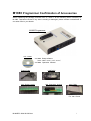
M1883 Programmer Confirmation of Accessories
When unpacking the package received from us, check if all the following items necessary for
M-1883 had been included. If any item is missing or damaged, please contact our distributor or
our sales office in your district.
M1883 Programmer
CD-ROM
・M1883 Setup software
(with USB driver、LPT driver)
・M1883 Operation Manual
Power Code
ZIP Socket POD1
USBCable
ISP Connector POD2
ISP Cable
For ISP Check
M1883EG-102A 201303.doc
i
For Safe Operation
Precaution for Safety
This operation manual includes safety indications here and there so that you can operate M1883
safety and correctly. For safe and correct operation of M1883 and also to prevent you, other
operators or workers from injury and property form damage, the following pictographs are used to
explain these safety indications.
Before reading this manual, fully understand these picotorgaphs and the meanings. Keep this
manual at hand refer to it as occasion arises.
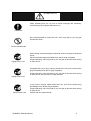
Explanation of Pictrographs
ii
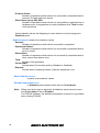
WARNING
Indicates a potential hazardous situation in which the
operator would be killed or seriously injured unless this
precaution is observed.
CAUTION
Indicates a potential situation in which the operator would
be injured or property would be damaged unless this
precaution is observed.
MINATO ELECTRONICS INC
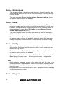
WARNING
When operating this unit, be sure to follow warnings and cautionary
instructions given by Minato Electronics Inc.
Compulsion
Do not disassemble or modify this unit. A fire may start or you may get
and electric shock.
Do Not Dissassemble
Unplug Power Cord
When finding a smoke,feeling an abnormal smell or hearing an abnormal
sound,
Pull out the power plug immediately from the AC plug receptacle.
If keep operating, a fire may start or you may get an electric shock owing
to short-circuit.
If dropped this unit or given a strong shock to the unit, pull out the power
plug immediately from the AC plug receptacle.
If keep operating, a fire may start or you may get an electric shock owing
to short-circuit. Consult with our repair window.
Unplug Power Cord
If any liquid or foreign matter enters this unit, pull out the power plug
immediately from the AC plug receptacle.
If keep operating, a fire may start or you may get an electric shock owing
to short-circuit.
Unplug Power Cord
Consult with our repair window.
M1883EG-102A 201303.doc
iii
WARRNING
This unit shall be operated by an operator who has fully understood the
operation manual of M1883.
Miss operation may damage this unit and other devices.
Compulsion
Before touching this unit, be sure to touch nearby large metal and
remove static electricity from your body so that this unit is not damaged
by static electricity.
Static electricity may damage this unit and other devices.
Compulsion
Clean the unit surface, the device socket and the air filter.
Operation without removing dusts from them will probably result in a fire
or a trouble. Try to clean them periodically.
Compulsion
Check the pass/fail judgement not only LED of programmer but also
Check sum on display of PC.
Compulsion
Attached AC cable is only used for Japan.
You need prepare for another suitable cable in your country.
Compulsion
iv
MINATO ELECTRONICS INC
Content
For Safe Opearation
Precaution for safety
Explanation of pictrograph
ⅴ--ⅷ
Content
For Users
How to use manual
Chapter 1
ⅱ
ⅱ
ⅱ
1
2
Outline of programmer、Specification、Installation
Outline of M1883
List of component
PC requirements
Feature of M1883 programmer
Update for programmer
4
4
5
6
9
Quick start
Installation of programmer software
Installation of programmer hardware
Run the control program
Programmimg a device
10
10
10
10
11
M1883 elements
12
Connection between M1883 to the PC
Using USB port
Using LPT port
13
13
13
In system serial programming by M1883
14
Selftest and calibration check
16
Technical specification
Hardware
Device support
Programming speed
Device operations
General
17
17
18
20
21
22
Installation
Software setup
Hardware setup
23
23
29
M1883EG-102A 201303.doc
v
Chapter 2
vi
M1883 Control Software((PG4UW) Operation Manual
M1883 Control software (PG4UW)
Explanation of maindisplay
33
34
File command
File / Load
File / Save
File / Load project
File / Save project
File / Reload file
File / Reload project
File / Project option
File / Load encryption table
File / Save encryption table
File / Exit without save
File / Exit and save
37
37
41
41
42
44
44
45
45
45
45
45
Buffer command
Buffer / View/Edit
Buffer / View/Edit for PLD
Buffer / Fill block
Buffer / Copy block
Buffer / Move block
Buffer / Swap data
Buffer / Erase
Buffer / Fill random data
Buffer / Duplicate buffer
Buffer / View/Edit / Print Buffer
Buffer / View/Edit / Find text
Buffer / View/Edit / Replace text
Buffer / Checksum
46
46
48
49
49
49
49
51
51
51
52
52
52
54
Device command
Device / Select from default devices
Device / Select device…
(All、Only selected type、Only selected manufacuter)
Device / Select EPROM / Flash by ID
Device / Device options
Device / Device options / Serialization
../../ Increment mode & SQTP
../../ From file mode
../../ Custom generator mode
Device / Device options / Statistics
Device / Device options / Associated file
Device / Device options / Specical options
58
58
58
59
61
62
66
67
74
80
85
87
87
MINATO ELECTRONICS INC
Device / Blank check
Device / Read
Device / Verify
Device / Program
Device / Erase
Device / Test
Device / IC test
Device / Jam/VME/SVF/…Player
Device / Device info
88
88
88
88
89
89
90
91
97
Programmer command
Programmer / Find programmer
Programmer / Refined programmer
Programmer / Module options
Programmer / Autmatic YES !
Programmer / Self test
Programmer / Self test plus
Programmer / Selftest ISP Connector
Programmer / Calibration test
98
98
98
98
99
101
101
101
102
Option command
Options / General option
(File option, File extensions, Buffer, Language,
Sound, Errors, Log file, Job Report, Automatic YES!,
Remote control, Save options, Other )
Options / View
(Main toolbar, Additional toolbar,
Device options before operation)
Options / Protected mode
Options / Multi-project
Options / Multi-project Wizard
Options / Save options
103
103
Help command
Help / Supported devices
Help / Supported Programmers
Help / Device list
(current programmer, all programmers,cross reference)
Help / Create problem report
Help / About
120
120
120
120
Warranty
122
M1883EG-102A 201303.doc
111
112
115
116
119
121
121
vii
viii
MINATO ELECTRONICS INC
For Users
We thank you for your purchase of our M1883.
The guarantee period of this unit is for one year after deliverly to you.
Even during the guarantee period, we exclude damages as a result of natural disaster,
Misoperation, modification or change of this unit by user and wear of the socket adapter
from the guarantee.
Also, please note that we are not obliged to refund for a damaged P-ROM of the programmer
due to malfunciton.
In case of anything unclear to you, please contact Mianto or Minato distributor.
Specifications are subject to change without prior for futher improvent.
M1883EG-102A 201303.doc
1
How to use this manual
This manual explains how to install the control program and how to use your programmer.
It is assumed that the user has some experience with PCs and installation of software.
Once you have installed the control program we recommend you consult the context
sensitive HELP within the control program rather than the printed User manual. Revisions
are implemented in the context sensitive help before the printed User manual.
Display
Function name using control software is displayed by thick character.
File->Load、File->Save、Buffer ->Display/Edit、
Tool button
Load 、 Save 、 Edit 、 Select 、....
Function key used on key board
<F1>、<F5>、etc.
Explanation of word
Device
ZIF socket
:any kind of programmable integrated circuits or programmable
devices
:Zero Insertion Force socket used for insertion of target device
Buffer
:part of memory or disk, used for temporary data storage
:type of PC port (parallel), which is primarily dedicated for
printer connection.
USB port
:type of PC port (serial), which is dedicated for connecting
portable and peripheral devices.
HEX data format:format of data file, which may be read with standard text viewers; e.g.
byte 5AH is stored as characters '5' and 'A', which mean bytes 35H and
41H. One line of this HEX file (one record) contains start address and
data bytes. All records are secured with checksum.
Printer port
2
MINATO ELECTRONICS INC
Chapter 1
Outline of programmer
Specification & Installration
M1883EG-102A 201303.doc
3
Outline of M1883
M1883 is a fast universal USB/LPT interfaced universal programmer and logic IC tester with
48 powerful pindrivers. Using build-in ISP connector the programmer is able to program ISP
capable chips in-circuit.
This design allows easily add new devices to the device list.
M1883 is a true universal and a true low cost programmer, providing one of the best "value for
money" in today's market.
M1883 work with almost any IBM PC Pentium compatible or higher, portable or desktop
personal computers. Programmers use the USB port or parallel (printer) port of PC.
Programmers function flawlessly on Windows operating system (see section PC requirement).
Programmers are driven by an easy-to-use, control program with pull-down menus, hot keys
and online help.
Please check component before you install control software and operate programmer.
In case there is missing item and defective item, please contact our sales office and local
distributor.
List of component
(1)
(2)
(3)
(4)
(5)
(6)
(7)
M1883 programmer
Electric cable
USB cable (1.5m)
Pod for self check of ZIF socket
Pod for self check of ISP connector
Flat cable for ISP check
CD ROM for control software
1set
1pc
1pc
1pc
1pc
1pc
1pc
Caution:Attached AC cable is used for domestic.
You need to prepare for AC suitable cable in your country.
4
MINATO ELECTRONICS INC
PC requirements
Minimam PC requirements
・OS
・CPU
・RAM
・Hard DisK
・Interface
・CD Drive
Microsoft Windows® XP
Pentiam 4
512MB
200MB
USB1.1
or Printer port[PP mode]
CD-ROM Reader
Reommmend PC requirements
・OS
・CPU
・RAM
・Hard Disk
・Interface
・CD Drive
M1883EG-102A 201303.doc
Microsoft Windows® 7
Core 2 Duo
1GB or more
Useful area 1GB or more
USB2.0
or Printer port[ECP、EPP mode]
CD-ROM Reader
5
Feature of M1883 programmer
M1883 is a very fast universal USB/LPT interfaced universal programmer built to meet the
strong demand of the small manufacturing and developer’s community for the fast and
reliable universal programmer.
M1883 support all kinds of types and silicon technologies of today and tomorrow
programmable devices without family-specific module. You have freedom to choose the
optimal device for your design. Using built-in in-circuit serial programming (ISP)
connector, the programmer is able to program ISP capable chips in circuit.
M1883 isn’t only programmer, but also tester of TTL/CMOS logic ICs and memories.
Furthermore, it allows generating user-definable test pattern sequences.
M1883 provides very competitive price coupled with excellent hardware design for reliable
programming. It is probably best "value for money" programmer in this class.
M1883 provides very fast programming due to high-speed FPGA driven hardware and
execution of time-critical routines inside of the programmer. It is at least fast than
competitors in this category, for many chips much faster than most competitors. As a
result, when used in production this one-socket-programmer waits for an operator, and
not the other way round.
M1883 interfaces with the IBM PC Pentium compatible or higher, portable or desktop
personal computers through USB (2.0/1.1) port or any standard parallel (printer) port.
Programmer can utilize power of both USB high-speed port and IEEE1284 (ECP/EPP)
high-speed parallel port. Support of both USB/LPT port connections gives you the choice
to connect the M1883 programmer to any PC, from latest notebook to older desktop
without USB port.
M1883 provides a banana jack for ESD wrist straps connection to easy-to-implement the
ESD protection control and also other banana jack for earth wire.
M1883 has a FPGA based totally reconfigurable 48 powerful TTL pindrivers, where
provide H/L/pull_up/pull_down and read capability for each pin of socket. Advanced
pindrivers incorporate high-quality high-speed circuitry to deliver signals without
overshoot or ground bounce for all supported devices. Improved pindrivers operate down
to 1.8V so you'll be ready to program the full range of today's advanced low-voltage
devices.
M1883 performs device insertion test (wrong or backward position) and contact check
(poor contact pin-to-socket) before it programs each device. These capabilities, supported
by overcurrent protection and signature-byte check help prevent chip damage due to
operator error.
The selftest capability allows running diagnostic part of software to thoroughly check the
health of the programmer.
Built-in protection circuits eliminate damage of programmer and/or programmed device
due environment or operator failure. All the inputs of the M1883 programmer, including the
6
MINATO ELECTRONICS INC
ZIF socket, ISP connector, connection to PC and power supply input, are protected
against ESD up to 15kV.
M1883 programmer performs programming verification at the marginal level of supply
voltage, which, obviously, improves programming yield, and guarantees long data
retention.
Various socket converters are available to handle device in PLCC, SOIC, PSOP, SSOP,
TSOP, TSSOP, TQFP, QFN (MLF), SDIP, BGA and other packages.
M1883 programmer is driven by an easy-to-use control program with pull-down menu,
hot keys and on-line help. Selecting of device is performed by its class, by manufacturer
or simply by typing a fragment of vendor name and/or part number.
Standard device-related commands (read, blank check, program, verify, erase) are
boosted by some test functions (insertion test, signature-byte check), and some special
functions (autoincrement, production mode - start immediately after insertion of chip into
socket).
All known data formats are supported. Automatic file format detection and conversion
during load of file.
The rich-featured autoincrement function enables to assign individual serial numbers to
each programmed device - or simply increments a serial number, or the function enables
to read serial numbers or any programmed device identification signatures from a file.
The software also provides a lot of information about programmed device. As a special,
the drawings of all available packages, explanation of chip labeling (the meaning of
prefixes and suffixes at the chips) for each supported chip are provided.
The software provide full information for ISP implementation: Description of ISP connector
pins for currently selected chip, recommended target design around in-circuit
programmed chip and other necessary information.
The remote control feature allows being PG4UW software flow controlled by other
application – either using .BAT file commands or using DLL file. DLL file, examples
(C/PAS/VBASIC/.NET) and manual are part of standard software delivery.
Jam files of JEDEC standard JESD-71 are interpreted by Jam Player. Jam files are
generated by design software which is provided by manufacturer of respective
programmable device. Chips are programmed in ZIF or through ISP connector (IEEE
1149.1 Joint Test Action Group (JTAG) interface).
VME files are interpreted by VME Player. VME file is a compressed binary variation of
SVF file and contains high-level IEEE 1149.1 bus operations. VME files are generated by
design software which is provided by manufacturer of respective programmable device.
Chips are programmed in ZIF or through ISP connector (IEEE 1149.1 Joint Test Action
Group (JTAG) interface).
Multiple devices are possible to program and test via JTAG chain: JTAG chain (ISP-Jam)
or JTAG chain (ISP-VME).
M1883EG-102A 201303.doc
7
Attaching of more M1883 programmers to the same PC (through USB port) is achieved
powerful multiprogramming systems, which support as many chips, as are
supported by M1883 programmer and without obvious decreasing of programming
speed. It is important to know, there is a concurrent multiprogramming - each
programmer works independently and each programmer can program different chip, if
necessary.
It is important to remember that in most cases new devices require only a software
update due to the M1883 is truly universal programmer. With our prompt service you can
have new devices can be added to the current list within hours!
8
MINATO ELECTRONICS INC
Update for programmer
Why is it important to use the latest version of the control program?
Semiconductor manufacturers continuously introduce new devices with new package types,
manufactured by new technologies in order to support the need for flexibility, quality and
speed in product design and manufacturing. To keep pace and to keep you up-to-date, we
usually implement more than 500 new devices into the control program within a year.
Furthermore, a typical programmable device undergoes several changes during its lifetime
in an effort to maintain or to improve its technical characteristics and process yields. These
changes often impact with the programming algorithms, which need to be upgraded (the
programming algorithm is a set of instructions that tells the programmer how to program
data into a particular target device). Using the newest algorithms in the programming
process is the key to obtaining high quality results. In many cases, while the older algorithm
will still program the device, they may not provide the level of data retention that would be
possible with an optimal algorithm. Failure to not use the most current algorithm can
decrease your programming yields (more improper programmed target devices), and may
often increase programming times, or even affect the long term reliability of the
programmed device.
At least, we are making mistakes too... .
Our commitment is to implement support for these new or modified parts before or as soon
as possible after their release, so that you can be sure that you are using latest and/or
optimal programming algorithms that were created for this new device.
M1883EG-102A 201303.doc
9
Quick start
Installation of programmer software
Run the installation program from the CD (Setup.exe) and follow the on-screen instructions.
Installation of programmer hardware
・connect the USB (or LPT) port of programmer to a USB (or printer) port of PC using supplied
cable
・connect the connector of the power supply adapter to the programmer or turn on programmer
by switch.
Run the control program
Double click on
After start, control program automatically scans all existing ports and searches for any
connected M1883. Program is common for all the M1883, hence program will try to find
M1883.
Menu File is used for source files manipulation, settings and viewing directory, changes
drives, changes start and finish address of buffer for loading and saving files and loading and
saving projects.
Menu Buffer is used for buffer manipulation, block operation, filling a part of buffer with string,
erasing, checksum and of course editing and viewing with other items (find and replace
string, printing...).
Menu Device is used for a work with selected programmable device: select, read, blank
check, program, verify, erase and setting of programming process, serialization and
associated file control.
Menu Programmer is used for work with programmer.
Menu Options is used to view and change various default settings.
Menu Help is used for view supported devices and programmers and information about
program version.
10
MINATO ELECTRONICS INC
Programming a device
1. select device: - ->
Select
click on
2. load data into buffer:
a) from file: - -> Load
click on
b)
from device: insert device to ZIF
and - -> Read click on
3. insert target device to ZIF
4. check, if the device is blank: - ->
Blank
5. program device: - ->
click on
Program
6. additional verify of device: - ->
M1883EG-102A 201303.doc
Verify
click on
click on
11
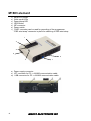
M1883 element
1)
2)
3)
4)
5)
6)
7)
48 pin ZIF socket
Work result LEDs
Power/sleep LED
YES! Button
ISP connector
Power switch
"GND" connector can be used for grounding of the programmer
"ESD wrist strap" connector is place for attaching of ESD wrist strap
1
3
2
5
6
4
7
8) Power supply connector
9) LPT connector for PC M1883 communication cable
10) USB connector for PC M1883 communication cable
12
MINATO ELECTRONICS INC
Connecting M1883 to the PC
Using USB port
In this case, order of connecting USB cable and power supply to programmer is
irrelevant.
Using LPT port
Switch off PC and programmer. Insert the communication cable included with your M1883
programmer package to a free printer port on your PC. If your computer is equipped with
only one printer port, substitute the programmer cable for the printer cable. Connect the
opposite cable end to the programmer. Screw on both connectors to counter-connectors.
This is very important. It may be uncomfortable to switch between printer cable and
programmer cable, though it is not recommended to operate the M1883 programmer
through a mechanical printer switch. Use of an electronic printer switch is impossible. But
you can install a second multi-I/O in your computer, thus obtaining a supplementary
printer port, says LPT2. So your printer may remain on LPT1 while the programmer on
LPT2.
Switch on the PC.
Connect the connector “8” to a mains plug using attached cable. At this time all 'work
result' LEDs (and 'POWER' LED) light up successive and then switch off. Once the
POWER LED lights with low brightness then the M1883 programmer is ready to run.
Next run the control program for M1883.
Caution! If you don't want to switch off your PC when connecting the M1883 proceed as
follows:
When connecting the programmer to the PC: FIRST insert the communications cable
and THEN the power-supply connector.
When disconnecting the programmer from the PC: FIRST disconnect the power-supply
connector and THEN the communication cable.
From M1883 point of view the connecting and disconnecting sequence is irrelevant.
Protection circuits on all programmer inputs keep it safe. But think of your PC please.
Problems related to the M1883 PC interconnection, and their removing
If you have any problems with M1883
Common
notes
please.
M1883EG-102A 201303.doc
13
In-system serial programming by M1883
For general definition, recommendation and direction about ISP see section Common notes
/ ISP please.
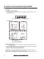
Description of ISP connector
As ISP connector is used 20 pins connector 2-1634689-0 from TE connectivity or other
compatible connector.
2
4
6
8
10 12 14 16 18 20
1
3
5
7
9
11 13 15 17 19
Front view at ISP connector of programmer.
H/L/read driver
pins 3, 5, 7, 9, 11, 13 of ISP connector
A)
pin 14 of ISP connector
B)
pin of ISP
connector
drivers in programmer
drivers in programmer
pin of ISP
connector
VCC
RA1
H/L
Float
RB2
Read
RA2
Pull-up/
Pull-down
RA3
RB1
YES!
GND
pins 15, 16 of ISP connector
C)
D)
drivers in programmer
CC1
pin of ISP
connector
Float
pin of ISP
connector
RD1
H/L
RC1
GND
E)
Read
CE1
Pull-up/
Pull-down
RC2
pin of ISP
connector
H/L
RE1
RA1 180R, RA2 1k3, RA3 22k,
RB1 10k, RB2 10k,
CC1 1n, RC1 1k3, RC2 22k,
RD1 22k, CE1 1n, RE1 1k3,
Comment to above picture:
picture C) Connection of pins 15 and 16 when are configured as logical signal needed for
ISP programming
pictures D) E) When pins 15 and 16 are configured as status of LED OK and LED ERROR
picture D) before first action with desired ISP device
picture E) after first action with desired ISP device
Notes: When LED OK or LED ERROR ON (shine), this status is presented as logical H,
level of H is 1,8V - 5V depend on H level of desired ISP device.
When LED OK or LED ERROR OFF (not shine), this status is presented as logical L, level of
14
MINATO ELECTRONICS INC
L is 0V - 0,4V.
The above mentioned values are provided to understand (and also to exactly calculate) the
value of resistors, which isolate (separate) the programmed chip and target system.
Specification of ISP connector pins depends on the device, which you want to program. You
can find it in the control SW (PG4UW) for programmer, menu Device / Device Info
(Ctrl+F1). Be aware, the ISP programming way of respective device must be selected. It is
indicated by (ISP) suffix after name of selected device.
Note: Pin no. 1 is signed by triangle scratch on ISP cable connectors.
As ISP connectors are used 20 pins connectors 09185207813 from Harting or other
compatible connector.
M1883 ISP cable
Warnings:
When you use M1883 as ISP programmer, don’t insert device to ZIF
socket.
When you program devices in ZIF socket, don’t insert ISP cable to ISP connector.
Use only attached ISP cable. When you use other ISP cable (other material,
length…), programming may occur unreliable.
M1883 can supply programmed device (pin 1 of ISP connector) and target system
(pin 5 of ISP connector) with limitation (see Technical specification / ISP connector).
M1883 apply programming voltage to target device and checks his value (target
system can modify programming voltage). If the programming voltage is different as
expected, no action with target device will be executed.
M1883EG-102A 201303.doc
15
Selftest and calibration check
If you feel that your programmer does not react according to your expectation, please run the
programmer (ISP connector) selftest using Diagnostic POD (Diagnostic POD for ISP
connectors #2), enclosed with the standard delivery package.
Selftest of programmer
Insert 48 pins diagnostic POD - type I into ZIF socket of the programmer. 48 pins
diagnostic POD - type I must be inserted as 48 pins device.
Run selftest of programmer in PG4UW (Programmer / Selftest plus).
Selftest of ISP connector
Insert Diagnostic POD for ISP connectors #2 into ZIF socket of the programmer.
Diagnostic POD for ISP connectors #2 must be inserted as 48 pins device.
Interconnect 20 pins connector of Diagnostic POD for ISP connectors #2 with an ISP
connector of the programmer with an ISP cable, included in delivery programmer package.
Be sure that pins are interconnected properly (i.e. 1-1, 2-2, ..., 20-20).
Run selftest of ISP connector in PG4UW (Programmer / Selftest ISP connector…).
16
MINATO ELECTRONICS INC
Technical specification
HARDWARE
Base unit, DACs
USB 2.0 high-speed compatible port, up to 480 Mb/s transfer rate
FPGA based IEEE 1284 slave printer port, up to 1MB/s transfer rate (except
BeeProg2C)
on-board intelligence: powerful microprocessor and FPGA based state machine
three D/A converters for VCCP, VPP1, and VPP2, controllable rise and fall time
VCCP range 0..8V/1A
VPP1, VPP2 range 0..26V/1A
selftest capability
protection against surge and ESD on power supply input, parallel port connection
banana jack for ESD wrist straps connection
banana jack for connection to ground
Socket, pindriver
48-pin DIL ZIF (Zero Insertion Force) socket accepts both 300/600 mil devices up to
48-pin
pindrivers: 48 universal
VCCP / VPP1 / VPP2 can be connected to each pin
perfect ground for each pin
FPGA based TTL driver provides H, L, CLK, pull-up, pull-down on all pindriver pins
analog pindriver output level selectable from 1.8 V up to 26V
current limitation, overcurrent shutdown, power failure shutdown
ESD protection on each pin of socket (IEC1000-4-2: 15kV air, 8kV contact)
continuity test: each pin is tested before every programming operation
ISP connector
20-pin male type with miss insertion lock
6 TTL pindrivers, provides H, L, CLK, pull-up, pull-down; level H selectable from 1.8V
up to 5V to handle all (low-voltage including) devices.
1x VCCP voltage (range 2V..7V/100mA)
programmed chip voltage (VCCP) with both source/sink capability and voltage sense
and 1x VPP voltage (range 2V..25V/50mA)
Target system power supply voltage (range 2V..6V/250mA)
ESD protection on each pin of ISP connector (IEC1000-4-2: 15kV air, 8kV contact)
two output signals, which indicate state of work result = LED OK and LED Error (active
level: min 1.8V)
input signal, switch YES! equivalent (active level: max 0.8V)
M1883EG-102A 201303.doc
17
DEVICE SUPPORT
Programmer, in ZIF socket
EPROM: NMOS/CMOS, 27xxx and 27Cxxx series, with 8/16 bit data width, full support
for LV series
EEPROM: NMOS/CMOS, 28xxx, 28Cxxx, 27EExxx series, with 8/16 bit data width
Flash EPROM: 28Fxxx, 29Cxxx, 29Fxxx, 29BVxxx, 29LVxxx, 29Wxxx, 49Fxxx series,
Samsung's K8Fxxxx, K8Cxxxx, K8Sxxxx, K8Pxxxx series, from 256Kbit to 1Gbit, with
8/16 bit data width, full support for LV series
NAND FLASH: Samsung K9xxx, Hynix HY27xxx, Toshiba TC58xxx, Micron MT29Fxxx,
Spansion S30Mxxx, Numonyx (ex STM) NANDxxx
LBA-NAND: Toshiba THGVNxxx
mDOC H3: SanDisk (ex M-Systems) SDED5xxx, SDED7xxx, MD2533xxx, MD2534xxx,
Hynix HY23xxx
Multi-chip devices: NAND+RAM, NOR+RAM, NOR+NOR+RAM, NAND+NOR+RAM
FRAM: Ramtron
MRAM: Everspin MRxxxxx8x
NV RAM: Dallas DSxxx, SGS/Inmos MKxxx, SIMTEK STKxxx, XICOR 2xxx, ZMD
U63x series
Serial E(E)PROM: Serial E(E)PROM: 11LCxxx, 24Cxxx, 24Fxxx, 25Cxxx, 59Cxxx,
85xxx, 93Cxxx, NVM3060, MDAxxx series, full support for LV series, AT88SCxxx
Serial Flash: standard SPI (25Pxxx, 25Fxxx, 25Lxxx, 25Bxxx, 25Txxx,25Sxxx, 25Vxxx,
25Uxxx, 25Wxxx, 45PExx), high performance Dual I/O SPI (25Dxxx, 25PXxxx), high
performance Quad SPI (25Qxxx, 26Vxxx), DataFlash (AT45Dxxx, AT26Dxxx)
Configuration (EE)PROM: XCFxxx, XC17xxxx, XC18Vxxx, EPCxxx, EPCSxxx,
AT17xxx, AT18Fxxx, 37LVxx
1-Wire E(E)PROM: DS1xxx, DS2xxx
PLD Altera: MAX 3000A, MAX 7000A, MAX 7000B, MAX 7000S, MAX7000AE, MAX
II/G/Z
PLD Lattice: ispGAL22V10x, ispLSI1xxx, ispLSI1xxxEA, ispLSI2xxx, ispLSI2xxxA,
ispLSI2xxxE, ispLSI2xxxV, ispLSI2xxxVE, ispLSI2xxxVL, LC4xxxB/C/V/ZC/ZE, M4-xx/xx,
M4A3-xx/xx, M4A5-xx/xx, M4LV-xx/xx, ispCLOCK, Power Manager/II, ProcessorPM
PLD: Xilinx: XC9500, XC9500XL, XC9500XV, CoolRunner XPLA3, CoolRunner-II
other PLD: SPLD/CPLD series: AMD, AMI, Atmel, Cypress, Gould, ICT, Lattice,
National Semicond., Philips, STMicroelectronics, TI (TMS), Vantis, VLSI
FPGA: Actel: ProASIC3, IGLOO, Fusion
FPGA: Lattice: MachXO, LatticeXP, ispXPGA
FPGA: Xilinx: Spartan-3AN
Clocks: TI(TMS), Cypress
Special chips: Atmel Tire Pressure Monitoring ATA6285N, ATA6286N, PWM
controllers: Zilker Labs, Analog Devices, Gamma buffers: TI, Maxim ...
Microcontrollers MCS51 series: 87Cxxx, 87LVxx, 89Cxxx, 89Sxxx, 89Fxxx, 89LVxxx,
89LSxxx, 89LPxxx, 89Exxx, 89Lxxx, all manufacturers,
Philips LPC series
Microcontrollers Intel 196 series: 87C196 KB/KC/KD/KT/KR/...
Microcontrollers Atmel ARM. ARM7: AT91SAM7Sxx, AT91SAM7Lxx, AT91SAM7Xxx,
AT91SAM7XCxx, AT91SAM7SExx series; ARM9: AT91SAM9xxx series; ARM
Cortex-M3: AT91SAM3Uxxx series
Microcontrollers Atmel AVR 8bit/16bit: AT90Sxxxx, AT90pwm, AT90can, AT90usb,
ATtiny, ATmega, ATxmega series
Microcontrollers Atmel AVR32: AT32UC3xxxx
Microcontrollers Chipcon (TI): CC11xx, CC24xx, CC25xx series
Microcontrollers Coreriver: Atom 1.0, MiDAS1.0, 1.1, 2.0, 2.1, 2.2, 3.0 series
18
MINATO ELECTRONICS INC
Serial E(E)PROM: IIC series, MW series, SPI series, KEELOQ series, PLD
configuration memories, UNI/O series
1-Wire E(E)PROM: DS1xxx, DS2xxx
Serial Flash: standard SPI (25xxx), DataFlash (AT45Dxxx, AT26Dxxx)
Microcontrollers Atmel: AT89Sxxx, AT90pwm, AT90can, AT90usb, AT90Sxxxx, ATtiny,
ATmega, ATxmega, AT89LSxxx, AT89LPxxx
Microcontrollers Atmel AVR32: AT32UC3xxxx
Microcontrollers Chipcon (TI): CC11xx, CC24xx, CC25xx series
Microcontrollers Cypress: CY8C2xxxx
Microcontrollers Elan: EM78Pxxx, EM6xxx series
Microcontrollers EM Microelectronic: 4 and 8 bit series
Microcontrollers Microchip PICmicro: PIC10xxx, PIC12xxx, PIC16xxx, PIC17xxx,
PIC18xxx, PIC24xxx, dsPIC, PIC32xxx series
Microcontrollers Mitsubishi: M16C
Microcontrollers Motorola/Freescale: HC08 (both 5-wire, All-wire), HC11, HC12,
HCS08, S12, S12X, MC56F, MCF52 series
Microcontrollers Nordic Semiconductor: nRF24xxx
Microcontrollers NEC: uPD7xxx series
Microcontrollers Philips (NXP): LPC1xxx, LPC2xxx, LPCxx series, 89xxx series
Microcontrollers Renesas: R8C/Tiny series
Microcontrollers Realtek, M-Square
Microcontrollers Scenix (Ubicom): SXxxx series
Microcontrollers STM: ST7xxx, STR7xx, STR9xx, STM32Fxx, STM8A/S/L series
Microcontrollers Silicon Laboratories(Cygnal): C8051 series
Microcontrollers & Programmable System Memory STMicroelectronics: uPSD, PSD
series
Microcontrollers TI: MSP430 (both JTAG and BSL series), MSC12xxx series
Microcontrollers ZILOG: Z8Fxxxx, Z8FMCxxxxx, Z16Fxxxx series, ZLF645x0xx
Various PLD (also by Jam/VME/SVF/STAPL/... Player/JTAG support):
Altera: MAX 3000A, MAX 7000A, MAX 7000B, MAX 7000S, MAX 9000, MAX II/G/Z
Xilinx: XC9500, XC9500XL, XC9500XV, CoolRunner XPLA3, CoolRunner-II
PLD Lattice: ispGAL22xV10x, ispLSI1xxxEA, ispLSI2xxxE, ispLSI2xxxV, ispLSI2xxxVE,
ispLSI2xxxVL, M4-xx/xx, M4LV-xx/xx, M4A3-xx/xx, M4A5-xx/xx, LC4xxxB/C/V/ZC/ZE,
ispCLOCK, Power Manager/II, ProcessorPM
FPGA: Actel: ProASIC3, IGLOO, Fusion
FPGA: Lattice: MachXO, LatticeXP, ispXPGA
Notes:
Devices marked * are obsolete, programming with additional module
For all supported devices see actual Device list on http://www.minato.co.jp/
I.C. Tester
TTL type: 54,74 S/LS/ALS/H/HC/HCT series
CMOS type: 4000, 4500 series
static RAM: 6116.. 624000
user definable test pattern generation
Package support
support all devices in DIP with default socket
package support includes DIP, SDIP, PLCC, JLCC, SOIC, SOP, PSOP, SSOP, TSOP,
TSOPII, TSSOP, QFP, PQFP, TQFP, VQFP, QFN (MLF), SON, BGA, EBGA, FBGA,
VFBGA, UBGA, FTBGA, LAP, CSP, SCSP etc.
support devices in non-DIP packages up to 48 pins with universal adapters
M1883EG-102A 201303.doc
19
programmer is compatible with third-party adapterMicrocontrollers Cypress:
CY7Cxxxxx, CY8Cxxxxx
Microcontrollers ELAN: EM78Pxxx
Microcontrollers Infineon(Siemens): XC800, C500, XC166, C166 series
Microcontrollers MDT 1xxx and 2xxx series
Microcontrollers Microchip PICmicro: PIC10xxx, PIC12xxx, PIC16xxx, PIC17Cxxx,
PIC18xxx, PIC24xxx, dsPIC, PIC32xxx series
Microcontrollers Motorola/Freescale: HC05, HC08, HC11, HC12, HCS08, RS08, S12,
S12X, MC56F, MCF51, MCF52 series
Microcontrollers Myson MTV2xx, 3xx, 4xx, 5xx, CS89xx series
Microcontrollers National: COP8xxx series
Microcontrollers NEC: uPD70Fxxx, uPD78Fxxx series
Microcontrollers Novatek: NT68xxx series
Microcontrollers Nuvoton (Winbond): N79xxx, W77xxx, W78xxx, W79xxx, W83xxx
series
Microcontrollers NXP ARM Cortex-M3: LPC13xx, LPC17xx series
Microcontrollers Philips (NXP) UOC series: UOCIII, UOC-TOP, UOC-Fighter series
Microcontrollers Philips (NXP) ARM7: LPC2xxx, PCD807xx, SAF7780xxx series
Microcontrollers Scenix (Ubicom): SXxxx series
Microcontrollers Renesas: R8C/Tiny series
Microcontrollers SGS-Thomson: ST6xx, ST7xx, ST10xx, STR7xx series
Microcontrollers SyncMOS: SM59xxx, SM73xxx, SM79xxx, SM89xxx series
Microcontrollers & Programmable System Memory STMicroelectronics: uPSD, PSD
series
Microcontrollers STM: ST6xx, ST7xx, ST10xx, STR7xx, STR9xx, STM32Fxx,
STM8A/S/L series
Microcontrollers Silicon Laboratories(Cygnal): C8051 series
Microcontrollers Texas Instruments: MSP430, MSC12xx series, TMS320F series
Microcontrollers Texas Instruments (ex Luminary Micro): LM3Sxxx, LM3Sxxxx series
Microcontrollers ZILOG: Z86/Z89xxx and Z8Fxxxx, Z8FMCxxxxx, Z16Fxxxx,
ZGP323xxxxxx, ZLF645xxxxxxx, ZLP12840xxxxx, ZLP323xxxxxxx series
Microcontrollers other: EM Microelectronic, Fujitsu, Goal Semiconductor, Hitachi,
Holtek, Novatek, Macronix, Princeton, Winbond, Samsung, Toshiba, Mitsubishi, Realtek,
M-Square, ASP, Coreriver, Gencore, EXODUS Microelectronic, Megawin, Syntek, Topro,
TinyARM, VersaChips, SunplusIT, Nordic, M-Square, QIXIN, Signetic, Tekmos,
Weltrend, Amic, Cyrod Technologies, Ember, Ramtron, Nordic Semiconductor,
Samsung ... EPROM:
NMOS/CMOS, 2708*
PROM: AMD, Harris, National, Philips/Signetics, Tesla, TI
Microcontrollers 48 series: 87x41, 87x42, 87x48, 87x49, 87x50 series
Microcontrollers 51 series: 87xx
Programmer, through ISP connector
s for non-DIP support
Programming speed
Device
H26M11002AAR
(eMMC NAND Flash)
K8P6415UQB (parallel NOR Flash)
K9F1G08U0M (parallel NAND Flash)
20
Size [bits]
3C780000hx8
(8 Giga)
400100Hx16
(64 Mega)
8400000Hx8
(1 Giga)
Operation
programming *1
Time
480 sec
programming and verify
13 sec
programming and verify
122.7 sec
MINATO ELECTRONICS INC
QB25F640S33 (serial Flash)
800200Hx8
programming and verify
(64 Mega)
AT89C51RD2 (microcontroller)
10000Hx8
programming and verify
PIC32MX360F512L (microcontroller)
80000Hx8
programming and verify
Conditions:
P4, 2,4GHz, 512 MB RAM, USB 2.0 HS, Windows XP
30.7 sec
14.4 sec
8.9 sec
Device operations
standard:
intelligent device selection by device type, manufacturer or typed fragment of part name
automatic ID-based selection of EPROM/Flash EPROM
blank check, read, verify
program
erase
configuration and security bit program
illegal bit test
checksum
interprete the Jam Standard Test and Programming Language (STAPL), JEDEC standard
JESD-71
interprete the VME files compressed binary variation of SVF files
security
insertion test, reverse insertion check
contact check
D byte check
special
production mode (automatic start immediately after device insertion)
lot of serialization modes (more type of incremental modes, from-file mode, custom
generator mode)
statistic
count-down mode
Buffer operations
view/edit, find/replace
fill/copy, move, byte swap, word/dword split
checksum (byte, word)
print
File load/save
no download time because programmer is PC controlled
automatic file type identification
Supported file formats
unformatted (raw) binary
HEX: Intel, Intel EXT, Motorola S-record, MOS, Exormax, Tektronix, ASCII-SPACE-HEX,,
ASCII HEX
Altera POF, JEDEC (ver. 3.0.A), e.g. from ABEL, CUPL, PALASM, TANGO PLD, OrCAD
PLD, PLD Designer ISDATA, etc.
JAM (JEDEC STAPL Format), JBC (Jam STAPL Byte Code), STAPL (STAPL File) JEDEC
standard JESD-71
VME (ispVME file VME2.0/VME3.0)
SVF (Serial Vector Format revision E)
STP (Actel STAPL file)
M1883EG-102A 201303.doc
21
GENERAL
operating voltage 100-250V AC
power consumption max. 20W active, about 2W sleep
dimensions 195x140x55 mm (7.7x5.5x2.2 inch)
weight 0.9kg (1.98 lb)
operating temperature 5°C ÷ 40°C (41°F ÷ 104°F)
operating humidity 20%..80%, non condensing
22
MINATO ELECTRONICS INC
Installation
The programmer package contains a CD with the control program, useful utilities
and additional information. The permission to freely copy the content of the CD is
granted in order to demonstrate how MINATO ELECTRONICS INC.'s
programmers work.
For programmers connected through USB (LPT) port, control program requires
correctly installed USB driver
We recommend install software before connecting programmer to PC to avoid
unwanted complication during installation.
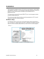
Software setup
Insert delivered CD to your CD drive and install program starts automatically (if
not, run setup.exe). Install program will guide you through the installation process
and will do all the necessary steps before you can first run the control program.
Set up 1
Click “Software installation PROGRAMMERS”button.
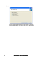
M1883EG-102A 201303.doc
23
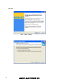
Set up 2
Click “Next” button.
24
MINATO ELECTRONICS INC
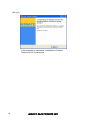
Set up 3
For change default folder click on “Browse” button, select the
destination folder.
Then click on “Next” button
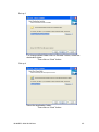
Set up 4
Select the destination folder.
Then click on “Next” button
M1883EG-102A 201303.doc
25
Set up 5
Check if “Install Multiprogramming control support” is selected.
Change default setting, if you want. Then click on “Next” button
26
MINATO ELECTRONICS INC
Set up 6
Check your setting and then click on “Install” button
Set up 7
Installation process will start.
M1883EG-102A 201303.doc
27
Set up 8
If this message is expressed、Installation is finished.
Please click on Finish button.
28
MINATO ELECTRONICS INC
Hardware setup
Warning: Because of high programmer's communication traffic, we recommend
to connect each programmer to separated USB 2.0 High speed controller (USB
EHCI). Most of new PC motherboards have two or more EHCI controller
integrated in chipset. If not, you can use PCI (PCI-E) USB add-on card (Renesas
USB chipset is recommended). If the EHCI integrated in motherboard chipset is
used, consult the motherboards manual or motherboard manufacturer tech
support for USB ports mapping so you will be able connect each programmer to
separated EHCI. In generally, we also recommend connect the programmers
directly to PC's USB ports (without USB HUB) and preferable to the USB ports
mounted on the motherboard directly (mostly located on the rear side of the PC).
When the programmer is connected to USB port before control program was
installed, Windows will detect new hardware and ask user to select driver
installation method: automatically or manually. To detect programmer correctly,
control program installation CD must be inserted to computer's CD-ROM drive
and following steps have to be done:
Step 1.
Directly connect USB (LPT) cable to type B USB (LPT) port on programmer.
Step 2.
Directly connect USB (LPT) cable to type A USB2.0 (LPT) port on PC
(high-speed recommended).
Step 3.
Connect connectors of power supply cable to appropriate connectors on
programmer and wall plug.
Step 4.
Turn on programmer. At this time all 'work result' LEDs light up successive and
then LEDs switch off.
For LPT connected programmer you may start work with your programmer now.
For USB connected programmer continue with next step.
M1883EG-102A 201303.doc
29
Step 5.
Windows will start with “Found new hardware wizard”.
For Windows XP, Service Pack 2 users only:
Select “No, not this time” and then click on “Next” button.
Select “Install the software automatically” and then
click on “Next” button.
30
MINATO ELECTRONICS INC
Step 6.
Click on “Continue Anyway” button.
Step 7.
Click “Finish” button to finish setup.
Step 8.
“Found new hardware wizard” will launch for each programmer one time.
Hardware setup will be continued with Step 5.
Note: If a different USB port on the PC is used for the next connection of
programmer, “Found new hardware wizard” will launch again and install new
USB drivers.
M1883EG-102A 201303.doc
31
Chapter 2
M1883 Cont Software (PG4UW)
Opetartion Manual
32
MINATO ELECTRONICS INC
M1883 Control Software (PG4UW)
Using the programmer software
The control program delivered by MINATO Electronics,
included on the CD in your package, is granted to be
free from any viruses at the moment of delivery. To
increase their safety our programs include a special
algorithm for detecting possible virus infections.
Execute M1883 control program (PG4UW)
In Windows environment: double click to icon
on display.
After start, control program automatically scan ports and search for the connected
M1883 programmer.
Notes: When PG4UW is started, program is checked for its integrity.
Then the program display a standard user menu and waits for your instructions.
If the control program cannot communicate with the programmer, an error
message appears on the screen, including error code and description of possible
reasons (disconnected programmer, bad connection, power supply failure,
incompatible printer port...). Eliminate the error source and press any key. If error
condition still exists, the program resumes its operation in the demo mode and
access to the programmer is not possible. If you cannot find the cause of the
error, follow the instructions in Troubleshooting section. In addition, the control
program checks communication with programmer prior to any operation with the
programmed device.
M1883EG-102A 201303.doc
33
Explanation of main display
Toolbars
Under main menu are placed toolbars with button shortcuts of frequently used
menu commands. Toolbars are optional and can be turned off by menu
command Options / View.
Log window
Log window contains the flow-control progress information about almost every
operation made in PG4UW.
Operation can be:
starting of PG4UW
programmer search
file/project load/save
selection of device
device operations (device read, blank check, programming, ...)
remote control application connection and disconnection
and other
Content of Log window can be saved to file concurrently while information is
written to Log window. This option can be set by menu Options / General
options (and tab Log file in dialog General options).
34
MINATO ELECTRONICS INC
Panel Addresses
Panel Addresses contains information about actual address ranges of currently
selected device, loaded file and buffer start-end address settings. Some devices
allow modifying default device and buffer address ranges by menu command
Device / Device options / Operation options.
Panel Addresses also contains some advanced information about current status
of Split, Serialization and buffer checksum. For more information about each of
the options, please look at:
Split - menu Device / Device options / Operation options
Serialization - menu Device / Device options / Serialization
Checksum - menu Buffer / Checksum at section Checksum displayed in main
window
Panel Programmer
Panel Programmer contains information about currently selected programmer.
The information includes
programmer type
port via programmer is connected to computer
programmer status, can be one of following
Ready - programmer is connected, successfully found and ready to work
Not found - programmer is not found
Demo - when user selects option (button) Demo in dialog Find programmer
YES! mode - some types of programmers allow to use special modes of
starting next device operation in one of following ways manually by control program dialog Repeat
manually by button YES! placed directly on programmer
automatically - programmer automatically detects device removing and
insertion of new device
For more details please look at Programmer / Automatic YES!.
Panel Device
It contains information about currently selected device.
The information includes
device name (type) and manufacturer
device adapter needed to use with currently selected programmer
reference to detailed Device info dialog, available also by menu Device /
Device info
reference to Advanced device options - this is available for some types of
devices only
Panel Statistics
It contains statistics information about currently selected device.
The information includes
number of successful, failure and total device operations
count-down status indicating number of remaining devices
Statistics and count-down options are available by menu command Device /
M1883EG-102A 201303.doc
35
Device options / Statistics or by mouse right click on panel Statistics and select
item Statistics from popup menu
Panel File
The panel is placed on the bottom of PG4UW main window. Panel shows urrently
loaded file or project name, size and date.
List of hot keys
<F1>
Help
Calls Help
<F2>
Save
Save file
<F3>
Load
Load a file into the buffer
<F4>
Edit
Viewing/editing of buffer
<F5>
Select/default Target-device selection from 10 last selected devices
list
<Alt+F5> Select/manual Target-device selection by typing device/vendor name
<F6>
Blank
Blank check
<F7>
Read
Reads device's content into the buffer
<F8>
Verify
Compares contents of the target device with the buffer
<F9>
Program
Programs target device
<Alt+Q> Exit without save
Terminates the M1883
<Alt+X> Exit and save Terminates the M1883 and saving
settings too
<Ctrl+F1>
Displays additional information about current device
36
<Ctrl+F2> Erase
Fill's the buffer with a given value
<Ctrl+Shift+F2>
Fill's the buffer with random values.
MINATO ELECTRONICS INC
File command
Menu File is used for source files manipulation, settings and viewing directory,
changes drives, changes start and finish address of buffer for loading and saving
files by binary, MOTOROLA, MOS Technology, Intel (extended) HEX,
Tektronix, ASCII space, JEDEC, and POF format. The menu commands for
loading and saving projects are located in this submenu too.
File / Load
Analyse file format and loads the data from specified file to the buffer. You can
choose the format desired
(binary, MOTOROLA, MOS Technology, Tektronix, Intel (extended)
HEX,
ASCII space, JEDEC and POF).
The control program stores a last valid mask for file listing. You can save the
mask into the config. file by command Options / Save options.
Note for special x16 formats:
Intel HEXx16 is Intel Hex file format with 16 bits data word for TMS320F
devices.
Motorola HEXx16 is Motorola file format with 16 bits data word for
TMS320F devices.
File formats description:
ASCII HEX format
Each data byte is represented as 2 hexadecimal characters, and is
separated by white space from all other data bytes. The address for data
bytes is set by using a sequence of $Annnn, characters, where nnnn is the
4-hex characters of the address. The comma is required. Although each
data byte has an address, most are implied. Data bytes are addressed
sequentially unless an explicit address is included in the data stream.
Implicitly, the file starts an address 0 if no address is set before the first
data byte. The file begins with a STX (Control-B) character (0x02) and
ends with a ETX (Control-C) character (0x03).
Note: The checksum field consists of 4 hex characters between the $S and
comma characters. The checksum immediately follows an end code.
Here is an example of ASCII HEX file. It contains the data "Hello, World" to
be loaded at address 0x1000:
^B $A1000,
48 65 6C 6C 6F 2C 20 57 6F 72 6C 64 0A ^C
$S0452,
M1883EG-102A 201303.doc
37
ASCII SPACE format
Very simple hex file format similar as ASCII HEX without checksum field,
without start (STX) and end (ETX) characters. Each data byte is
represented as 2 hexadecimal characters, and is separated by white space
from all other data bytes. The address field is separated by white space
from data bytes. The address is set by using a sequence of 4-8 hex
characters.
Here is an example of ASCII SPACE file. It contains the data "Hello, World"
to be loaded at address 0x1000:
0001000 48 65 6C 6C 6F 2C 20 57 6F 72 6C 64 0A
Straight HEX format
Very simple hex file format similar as ASCII HEX without address and
checksum fields, without start (STX) and end (ETX) characters. Each data
byte is represented as 2 hexadecimal characters, and is separated by
white space from all other data bytes.
Here is an example of Straight HEX file. It contains the data "Hello, World":
48 65 6C 6C 6F 2C 20 57 6F 72 6C 64 0A
Samsung HEX format
Samsung HEX file format is slight modification of Intel HEX format,
therefore in the software is recognized and indicated as Intel HEX file
format.
Checking the check box Automatic file format recognition tells program
to detect file format automatically. When program can't detect file format
from one of supported formats, the binary file format is assumed.
When the check box Automatic file format recognition is unchecked
program allows user to manually select wished file format from list of
available file formats on panel Selected file format. Default set is from
Options / General options in panel Load file format at tab File options.
Attention: Program doesn't know recognize files in ASCII Hex format
automatically, it recognizes them as binary. So download files in ASCII Hex
format with disabled option for automatic file format recognition.
Additional operation
Panel Additional operation contains following settings:
Erase buffer before loading - checking the check box Erase buffer before
loading tells the program to erase all buffer data using entered Erase
value. Buffer erase is performed immediately before reading file content to
buffer and it is functional for binary and all HEX file formats. Using this
one-shot setting disables current setting of Erase buffer before loading
38
MINATO ELECTRONICS INC
option in menu Options / General options at tab Hex file options
Swap bytes - if checked, it activates function of swapping bytes within 16bit
words (or 2-byte words) during reading of file. This feature is useful
especially when loading files with Motorola representation of byte order in
file (big endian). Standard load file is using little endian byte order. For
more information about big endian and little endian see Big endian and
Little endian..
Add blank spare area - (for NAND Flash devices) if checked, adds blank
spare area data during file load to relevant position in buffer (dependent on
selected device).
Buffer offset for loading
Panel Buffer offset for loading contains one-shot offset setting for loading
data from file to buffer. The setting is used to specify optional offset of loaded
data to store to buffer. When Load file dialog window is opened, offset has
always default setting None. It means, no offset is used to store read data in
buffer.
Available offset options are:
None
Positive offset
Negative offset
this setting means, no offset is applied for loading data
from file to buffer.
set of offset value, which is added to current address to
store data to buffer. This offset is available for all formats
and is used in x8 format, if current buffer organization is
x8, or in x16 format, if current buffer organization is x16.
mode has two options:
Negative offset and Automatic negative offset
- set by two ways: manual or automatic.
For manual set use option Negative offset and put wished offset value to
its edit box.
For automatic offset detection use option Automatic negative offset.
This value is subtracted from current address for save data to buffer.
Negative offset value (manually defined or automatically detected) is
subtracted from current buffer address for store data to buffer.
Negative offset is applied only for all HEX file formats and is using always
x8 format. Negative offset settings are ignored for binary files and other
non-HEX files.
Notes for negative offset settings:
Since the value of negative offset is subtracted from real address, the result
fsubtraction can be negative number. Therefore take care of correct setting of
this value!
M1883EG-102A 201303.doc
39
We recommend automatic set of negative offset in special cases only. This
option contains a heuristic analyze, which can treat some data in file
incorrectly. There are especially critical files, which contain a fragmented
addresses range and which exceeds a size of selected device - some block
can be ignored.
Automatic negative offset option is not available for some kinds of special
devices, that require HEX files with exactly specified blocks used for the
devices - for example Microchip PICmicro devices. For these special devices,
there are available only manual offset settings (None, Positive offset, Negative
offset).
Example for negative offset using:
A file contains data by Motorola S - format.
A data block started at address FFFF0H.
It is a S2 format with length of address array of 3 bytes.
For all data reading you can set Negative offset option and value of negative
offset to FFFF0H.
It means, that the offset will be subtracted from current real addresses and so
data will be written from buffer address 0.
List of file format codes and error codes
There can occur some errors during file download in some of supported formats. The
error is written to LOG window in face "Warning: error #xxy in line rrr", xx is file format
code, y is error code and rrr is line number in decimal.
File format codes:
#00y - binary
#10y - ASCII Space
#20y - Tektronix
#30y - Extended tektronix
#40y - Motorola
#50y - MOS Technology
#60y - Intel HEX
Load file error codes:
#xx1 - bad first character - header
#xx2 - bad character in current line
#xx3 - bad CRC
#xx4 - bad read address
#xx5 - bad length of current line
#xx6 - too big negative offset
#xx7 - address is out of buffer range
#xx8 - bad type of selected file format
#xx9 - the file wasn't loaded all
40
MINATO ELECTRONICS INC
File / Save
Saves data in the buffer, which has been created, modified, or read from a
device onto a specified disk. The file format of saved file can be chosen from
supported formats list box. There can be also entered the Buffer start and
Buffer end addresses which exactly specify part of buffer to save to file.
Supported file formats now are binary, MOTOROLA, MOS Technology,
Tektronix, Intel (extended) HEX, ASCII space, JEDEC and POF.
If the checkbox Swap bytes is displayed, the user can activate function of
swapping bytes within 16bit words (or 2-byte words) during writing to file. This
feature is useful especially when saving files with Motorola representation of
byte order in file (big endian). Standard save file operation is using little endian
byte order.
For more information about big endian and little endian see Big endian and
Little endian.
File / Load project
This option is used for loading project file, which contains device configuration
buffer data saved and user interface configuration.
The standard dialog Load project contains additional window - Project
description - placed at the bottom of dialog. This window is for displaying
information about currently selected project file in dialog Load project.
Project information consists of:
manufacturer and name of the first device selected in the project
date and time of project creation
user written description of project (it can be arbitrary text, usually author of
project and some notes)
Note: for projects with serialization turned on
Serialization is read from project file by following procedure:
1. Serialization settings from project are accepted
2. Additional serialization file search is performed. If the file is found it will
be read and serialization settings from the additional file will be accepted.
Additional serialization file is always associated to the specific project file.
When additional serialization file settings are accepted, project
serialization settings are ignored.
Name of additional serialization file is derived from project file name by adding
extension ".sn" to project file's name.
Additional serialization file is always placed to the directory "serialization¥" into
the control program's directory.
M1883EG-102A 201303.doc
41
Example:
Project file name: my_work.prj
Control program's directory: c:¥Program Files¥Programmer¥
The additional serialization file will be:
c:¥Program Files¥Programmer¥serialization¥my_work.prj.sn
Additional serialization file is created and refreshed after successful device
program operation. The only requirement for creating additional serialization
file is load project with serialization turned on.
Command File / Save project deletes additional serialization file, if the file
exists, associated with currently saved project.
Enter job identification dialog
The dialog will be showed when loading protected project files.
It contains two editable fields:
Operator identification - this parameter will be used to identify rogrammer's
operator. Operator ID must be at least 3 chars. User has to enter perator
identification value, because it is mandatory parameter, when creating
Job Report for protected project.
Enter Job ID - identification of current job.
Note: Dialog Enter job identification is not password dialog. Values of
Operator identification and Job ID have informative purpose only, they
will be included in Job Report. It does not relate to protected and/or
encrypted project passwords.
File / Save project
This dialog is used for project file saving. Project file contains settings of
device configuration and buffer data. Data saved to project file can be
restored anytime by menu command File / Load project.
Description of actually selected project in file list box
Displays information about existing project file currently selected in dialog Save
project. This box is only for information and is not writable.
Description of project being saved
Upper half displays information about actual program configuration including
currently selected device, program mode, date and time, etc., and is not
writable. These actual program settings are used for creation of project
description header.
42
MINATO ELECTRONICS INC
Bottom half is user editable and contains project description (arbitrary text)
which usually consists of project author and some notes.
Prodduct protection setting
Encrypt project file (with password) is used to save project in special format
using encryption algorithm. This prevents loading project file into software
without knowledge of password. After clicking the button with key, password
dialog appears, which is used to specify encryption password for project being
saved.
Set Protected mode of software after loading of this project file is used to
save project in special mode called Protected mode. After clicking the button
with key, password dialog appears, which is used to specify Protected mode
password for project being saved, and another security options (disable other
project loading, device operations restriction) to prevent operator's mistakes.
Projects saved with active Protected mode are special projects called
Protected mode projects. For more detailed information about Protected
mode projects see Options / Protected mode
Recommendation: passwords for Encrypt project file (with password) and
Set Protected mode of software after loading of this project file should not
be the same.
Require project file checksum before first programming
when active, software asks user for entering correct project file unique ID,
before allowing to start the first device programming after load project. This
feature is recommended for additional check, that correct project file is
recently loaded. There is also recommended to use this checkbox along with
active Protected mode. When the request of project file unique ID is active,
the software indicates this by label (ID) next to project file name in bottom
status line in control program main window.
Note: Option Require project file unique ID before first programming is
replacement of former Require project file checksum before first
programming. Unique ID advantage over generic checksum is, that
unique ID is calculated not just from main device buffer data, but also
from secondary buffers data used by device and available device
settings. When the request of project file checksum is active, the
software indicates this by label (CSum) next to project file name in
bottom status line in control program main window. This option is no
longer available in Save project dialog, but it can be activated after
loading of older project file, that has the checksum request set on.
M1883EG-102A 201303.doc
43
Fig. Save project dialog
File / Reload file
Choose this option to reload a recently used file.
When you use a file, it is added to the Reload file list. Files are listed in order
depending on time of use of them. Lastly used files are listed before files used
far off.
To Reload a file:
1. From the File menu, choose Reload file.
2. List of lastly used files is displayed. Click the file you want to reload.
Note: When reloading a file the file format is used, by which the file was lastly
loaded/saved.
File / Reload project
Choose this option to reload a recently used project.
When you use a project, it is added to the Reload project list. Projects are
listed in order depending on time of use of them. Lastly used projects are
listed before projects used far off.
44
MINATO ELECTRONICS INC
To Reload a project:
1. From the File menu, choose Reload project.
2. List of lastly used projects is displayed. Click the project you want to
reload.
File / Project options
This option is used for display/edit project options of actually loaded project.
Project options means basic description of project including following project
data:
device name and manufacturer
project creation date
user defined project description (arbitrary text), e.g. project author and other
text data for more detailed project description
User can directly edit user defined project description only. Device name,
manufacturer, project date and program version are generated automatically
by program.
File / Load encryption table
This command loads the data from binary file from disk and it saves them into
the part of memory, reserved for an encryption (security) table.
File / Save encryption table
This command writes the content of the memory's part, reserved for an
encryption table, into the file on the disk as a binary data.
File / Exit without save
The command deallocates heap, cancels buffer on disk (if exists) and returns
back to the operation system.
File / Exit and save
The command deallocates heap, cancels buffer on the disk (if exists), saves
current setting of recently selected devices to disk and returns back to the
operation system.
M1883EG-102A 201303.doc
45
Buffer command
Menu Buffer is used for buffer manipulation, block operation, filling a part of
buffer with string, erasing, checksum and of course editing and viewing with other
items (find and replace string, printing...).
Buffer / View/Edit
This dialog is used to view (view mode) or edit (edit mode) data in buffer. Use
arrow keys for select data for edit. The data in buffer outside of area where are
located data for the selected chip are shown using gray background.
View/Edit Buffer
F1
display help for actual window
F2
Ctrl+F2
fill buffer block specified by start and end addresses by
requested hex (or ASCII) string
erase buffer with specified blank value
Ctrl+Shift+F2 fill buffer with random data
F3
46
copy specified block of buffer data at new address. Target
address needn't be out from source block addresses.
Shift+F2
save buffer data to binary file. This command is available for
secondary buffers only. Secondary buffers are special areas
used for some devices, for example Data EEPROM for
Microchip PICmicro devices. Commands for Load/Save data
to/from Main buffer are available in main menu "File" and also by
buttons Load, Save in main application window.
Shift+F3
load data from binary file to buffer. This command is available for
secondary buffers only. For more information see notes for save
buffer data command (Shift+F2) above
F4
move block is used to move specified block of data in current
buffer on new address. Target address needn't be out from
source block addresses. Source address block (or part) will be
filled by topical blank character.
F5
swap bytes command swaps a high- and low- order of byte pairs
in current buffer block. This block must started on even address
and must have an even number of bytes. If this conditions do not
fulfil, the program modifies addresses itself (start address is
moved on lower even address and/or end address is moved on
higher odd address).
MINATO ELECTRONICS INC
F6
print buffer
F7
find string (max. length 16 ASCII characters)
F8
find and replace string (max. 16 ASCII chars.)
F9
change current address
F10
change mode view / edit
F11
switch the mode of buffer data view between 8 bit and 16 bit
view. It can be also do by mouse clicking on the button to the
right of View/Edit mode buffer indicator. This button indicates
actual data view mode (8 bit or 16 bit), too.
F12
checksum dialog allows to count checksum of selected block of
buffer change mode view / edit
Arrow keys
Home/End
PgUp/PgDn
Ctrl+PgUp/PgDn
Ctrl+Home/End
Shift+Home/End
Backspace
move cursor up, down, right and left
jump on start / end current line
jump on previous / next page
jump on start / end current page
jump on start / end current device
jump on start / end current buffer
move cursor one position left (back)
Note: characters 20H - FFH (mode ASCII) and numbers 0..9, A..F (mode HEX)
immediately changes content of edit area.
Warning: Editing of ASCII characters for word devices is disabled.
M1883EG-102A 201303.doc
47
View/Edit buffer for PLD
Ctrl+F2
erase buffer with specified blank value
Ctrl+Shift+F2 fill buffer with random data
F9
go to address...
F10
change mode view / edit
F11
switch the mode of buffer data view between 1 bit and 8 bit view.
It can be also do by mouse clicking on the button to the right of
View/Edit mode buffer indicator. This button indicates actual
data view mode (1 bit or 8 bit), too.
Arrow keys
Home/End
PgUp/PgDn
Ctrl+PgUp/PgDn
Ctrl+Home/End
Backspace
move cursor up, down, right and left
jump on start / end current line
jump on previous / next page
jump on start / end current page
jump on start / end edit area
move cursor one position left (back)
Note: Characters 0 and 1 immediately changes content of edit area.
48
MINATO ELECTRONICS INC
Buffer / Fill block
Selecting this command causes filling selected block of buffer by requested
hex (or ASCII) string.
Selecting option "Allow address history logging" activates saving of recently
confirmed values. These are saved for each device separately, count is limited
to last 15 items.
Note: Address history values are common for all buffer data manipulation
dialogs.
Default address range is set according to buffer range of selected device.
Selecting option "Maintain last inserted values" causes that for the next time
you open this dialog, previously confirmed values will be reloaded as default.
Buffer / Copy block
This command is used to copy specified block of data in current buffer on new
address. Target address needn't be out from source block addresses.
Buffer / Move block
This command is used to move specified block of data in current buffer on new
address. Target address needn't be out from source block addresses. Source
address block (or part) will be filled by topical blank character.
Selecting option "Allow address history logging" activates saving of recently
confirmed values. These are saved for each device separately, count is limited
to last 15 items.
Note: Address history values are common for all buffer data manipulation
dialogs.
Default address range is set according to buffer range of selected device.
Selecting option "Maintain last inserted values" causes that for the next time
you open this dialog, previously confirmed values will be reloaded as default.
Buffer / Swap block
This command swaps a high- and low- order of byte pairs,
foursomes, nibbles inside bytes or bits inside bytes depending on swap
mode selected by user. Swap operation is performed on buffer block specified
by Start and End addresses. This block must start on even address and must
have an even number of bytes. If the conditions do not fulfill, the program
modifies addresses itself (start address is moved on lower even address
and/or end address is moved on higher odd address).
M1883EG-102A 201303.doc
49
Following swap modes are available, user can select from:
1. Swap 2-bytes inside 16-bit words
This option makes swap of byte pairs inside 16-bit words.
2. Swap 4-bytes inside 32-bit words
This option makes swap of byte pairs inside 32-bit words.
3. Swap nibbles inside bytes
This option makes swap of high- and low- nibbles inside each byte.
4. Mirror bits inside bytes
This option makes mirroring of bits inside each byte.
Examples of swap operation in buffer:
Swap bytes operation from Start address 0 to End address N modifies data in
buffer by following tables:
Address
Original
Buffer Data
Swap
2-bytes inside
16-bit words
Swap
4-bytes inside
32-bit words
Swap
nibbles
inside bytes
Mirror bits
inside bytes
0000h
0001h
0002h
0003h
0004h
0005h
0006h
0007h
b0
b1
b2
b3
b4
b5
b6
b7
b1
b0
b3
b2
b5
b4
b7
b6
b3
b2
b1
b0
b7
b6
b5
b4
b0n
b1n
b2n
b3n
b4n
b5n
b6n
b7n
b0m
b1m
b2m
b3m
b4m
b5m
b6m
b7m
b0, b1, b2, ... means original buffer byte values from addresses 0, 1, 2, ...
b0n, b1n, b2n, ... means nibble-swapped original bytes b0, b1, b2, ... by
following rules:
Original Byte bits
bit 7 bit 6 bit 5 bit 4 bit 3 bit 2 bit 1 bit 0
Nibble-swapped Byte Bits bit 3 bit 2 bit 1 bit 0 bit 7 bit 6 bit 5 bit 4
Original Byte bits
Mirrored Byte Bits
bit 7
bit 0
bit 6
bit 1
bit 5
bit 2
bit 4
bit 3
bit 3
bit 4
bit 2
bit 5
bit 1 bit 0
bit 6 bit 7
Selecting option "Allow address history logging" activates saving of recently
confirmed values. These are saved for each device separately, count is limited
to last 15 items.
Note: Address history values are common for all buffer data manipulation
dialogs.
50
MINATO ELECTRONICS INC
Default address range is set according to buffer range of selected device.
Selecting option "Maintain last inserted values" causes that for the next time
you open this dialog, previously confirmed values will be reloaded as default.
Buffer / Erase block
If this command is selected, the content of the buffer will be filled with topical
blank character.
Selecting option "Allow address history logging" activates saving of recently
confirmed values. These are saved for each device separately, count is limited
to last 15 items.
Note: Address history values are common for all buffer data manipulation
dialogs.
Default address range is set according to buffer range of selected device.
Selecting option "Maintain last inserted values" causes that for the next time
you open this dialog, previously confirmed values will be reloaded as default.
The reserved key <Ctrl+F2> will bring out this menu from any menu and any
time.
Buffer / Fill block with random data
If this command is selected, the content of the buffer will be filled with random
data.
Selecting option "Allow address history logging" activates saving of recently
confirmed values. These are saved for each device separately, count is limited
to last 15 items.
Note: Address history values are common for all buffer data manipulation
dialogs.
Default address range is set according to buffer range of selected device.
Selecting option "Maintain last inserted values" causes that for the next time
you open this dialog, previously confirmed values will be reloaded as default.
The reserved key <Shift+Ctrl+F2> will bring out this menu from any menu and
any time.
Buffer / Duplicate buffer
This command performs duplicate buffer content in range of source EPROM to
range of destination EPROM. This procedure is suitable if there is used for
example 27C512 EPROM to 27C256 EPROM position.
Note: The procedure always uses buffer start address 00000h.
M1883EG-102A 201303.doc
51
Buffer / View/Edit / Print buffer
This command allows write selected part of buffer to printer or to file. Program
uses at it an external text editor in which selected block of buffer is displayed
and can be printed or saved to file, too. By default is set simple text editor
notepad.exe, which is standard part of all versions of Windows.
In Print buffer dialog are following options:
Block start
Defines start address of selected block in buffer.
Block end
Defines end address of selected block in buffer.
External editor
This item defines path and name of external program, which has to be used as
text viewer for selected block of buffer. By default is set simple text editor
notepad.exe, which is standard part of all versions of Windows. User can
define any text editor for example wordpad.exe, which is able to work with
large text files. In user defined text editor user can print or save to file selected
block of buffer.
The external editor path and name is saved automatically to disk.
Buffer / View/Edit
/ Find text
Find to text
Enter the search string to Find to text input box and choose <Find> to begin
the search or choose <Cancel> to forget it.
Direction
Direction box specifies which way you want to search, starting from the current
cursor position (In edit mode). Forward (from the current position or start of
buffer to the end of the buffer) is the default. Backward searches toward the
beginning. In view mode searches all buffer.
Origin
Origin specifies where the search should start.
Buffer / View/Edit
/ Replace text
Text to find
Enter the search string in the Text to find string input box.
Replace with
Enter the replacement string in the Replace with input box.
Options
In Options box you can select prompt on replace: if program finds instance you
will be asked before program change it.
52
MINATO ELECTRONICS INC
Direction
Direction box specifies which way you want to search, starting from the current
cursor position (In edit mode). Forward (from the current position or start of
buffer to the end of the buffer) is the default. Backward searches toward the
beginning. In view mode searches all buffer.
Press <Esc> or click Cancel button to close dialog window.
Origin
Origin specifies where the search should start.
By pressing Replace button the dialog box is closed and a Question window is
displayed.
This window contains following choices:
Yes
No
Replace All
Abort search
M1883EG-102A 201303.doc
replaces found item and finds next
finds next item without replacing current one
replaces all found items
aborts this command
53
Buffer / Checksum
Checksum of data stored in buffer of PG4UW is useful to check the data are
correct.
PG4UW contains following functions related to checksum:
Tab Checksum calculator
This tab is on-demand checksum calculator that can calculate and display
various types of checksums of various data blocks in buffer. (*1)
Tab Main checksum options
This tab contains options for Automatic checksum calculator with Main
checksum value displayed in main window of PG4UW in table Addresses
and in Log window of PG4UW (*2)
Checksum calculator
contains on-demand checksum calculator. (*1)
Custom address range for chksum calculation
Fields From address and To address are used to enter address range for
main checksum calculation. Addresses are used only when checkbox
Enabled is checked. Address is always defined as Byte address.
Buffer block(s) exclude from checksum calculation
Useful for example for serialization. Serialization usually modifies data at
specified addresses in buffer. So there is problem to check the checksum
of buffer, when data on some addresses were changed by serialization
engine before each device programming. If part of buffer (data block) used
for serialization is excluded from checksum calculation, the checksum of
buffer data will not be changed by serialization data changes. One or more
excluded blocks can be specified.
Results
Fields displaying values of calculated checksum types: see description of
types at the bottom.
Column marked as STRAIGHT is result of checksum calculation
without additional adjustments.
Column marked as NEGATED is a negation of checksum so, that SUM
+ NEG. = FFFFH.
Column marked as SUPPLEMENT is complement of checksum so, that
SUM + SUPPL. = 0 (+ carry).
Insert checksum options
This box contains following options for Calculate & insert operation:
54
MINATO ELECTRONICS INC
- Insert checksum
Kind of checksum that is written into the buffer when, the Calculate &
insert operation was executed.
- Insert at address
Address in buffer where a result of chosen checksum is written, when the
Calculate & insert was executed. Address can not be specified inside the
range <From address> to <To address>. Address is always defined as
Byte address.
- Size
Size of chosen checksum result, which will be written into the buffer. A
size of inserted checksum may be Byte (8-bit), Word (16-bit) or DWORD
(32-bit). If size is smaller then selected checksum size, only lower byte(s)
of checksum value will be written into the buffer.
Note: If Word size was selected, a low byte of checksum value will be
written on address specified in box Insert address and a high byte will be
written on address incremented by one. Similarly it is for DWORD.
Calculate button - click on the button Calculate starts calculating checksums
for selected block in buffer. No writes into the buffer are executed.
Calculate & insert button - click on the button Calculate & insert starts
calculating checksums for selected block in the buffer and writes the
chosen checksum into the buffer on address specified by Insert address.
This function is available for Byte, Word, CRC-CCITT and CRC-XMODEM
checksums.
Close button - closes dialog Checksum.
(*1) These values aren't saved into project, they are initialized to defaults with
each new device selection.
Main checksum options
allows you to set mode of Automatic checksum calculator. (*2)
Custom address range for main checksum
Enabled - user defined addresses are used to calculate checksum of
buffer data, otherwise,
if Disabled, global Buffer start and Buffer end address is used for
calculation of checksum of buffer data
Fields From address and To address are used to enter address range for
main checksum calculation. Addresses are used only when checkbox
Enabled is checked.
Checksum type
M1883EG-102A 201303.doc
55
Selection group Checksum type allows to select wished kind of checksum
to be used for main checksum. More information about Checksum types
can be found at the bottom of this page.
Buffer block(s) exclude from checksum calculation
Exclude buffer block(s) from checksum calculation - same as for Tab
Checksum calculator
Result contains actual value of recently calculated checksum.
Apply button is used to confirm checksum settings from Main checksum
options. Please note, that once the button is pressed, previous checksum
settings are lost.
Close button is used to close the Checksum dialog. If you made some
changes in settings, they won't take effect until you press Apply.
(*2) These values are stored into configuration file and project file. Setting from
project file has higher precedence.
Checksum types
Byte sum (x8)
Buffer data are summed byte-by-byte irrespective of current buffer view
mode (x8/x16/x1) organization. Any carry bits exceeding 32-bits are
neglected. This checksum mode is indicated by string (x8) displayed after
checksum value in main program window.
Word sum Little Endian (x16)
Buffer data are summed word-by-word irrespective of current buffer view
mode organization. Any carry bits exceeding 32-bits are neglected. This
checksum mode is indicated by string (x16 LE) displayed after checksum
value in main program window. Term Little Endian means, the buffer
checksum is calculated from words read from buffer in Little Endian mode.
Word sum Big Endian (x16)
Buffer data are summed word-by-word irrespective of current buffer view
mode organization. Any carry bits exceeding 32-bits are neglected. This
checksum mode is indicated by string (x16 BE) displayed after checksum
value in main program window. Term Big Endian means, the buffer
checksum is calculated from words read from buffer in Big Endian mode.
CRC-CCITT
Buffer data are summed by bytes to Word using polynomial
x^16+x^12+x^5+1 (0x1021), init value 0, and XOR out 0, reflexions in/out
are off
CRC-XMODEM
Buffer data are summed by bytes to Word using polynomial x^16 + x^15 +
x^2 +1 (0x8005), init value 0
56
MINATO ELECTRONICS INC
CRC-16
Buffer data are summed by bytes to sum by bytes to WORD using standard
CRC-16 algorithm with polynome x^16+x^15+x^2+1 (0x8005), init value 0,
and XOR out 0
CRC-32
Buffer data are summed by bytes to DWORD using standard CRC-32
algorithm with polynome 0x04C11DB7, init value 0xFFFFFFFF, and XOR
out 0xFFFFFFFF
MD5
an MD5 hash expressed as a sequence of 32 hexadecimal digits (128 bits)
SHA-1
"Secure Hash Standard" expressed as a sequence of 40 hexadecimal
digits (160 bits)
Checksum forms
Straight
checksum without additional adjustments.
Negated
negation of checksum so, that SUM + NEG. = FFFFH.
Supplement
is complement of checksum so, that SUM + SUPPL. = 0 (+ carry).
Device dependent checksum
applies for some devices, e.g. STMicroelectronics's STM8 family The
checksum modes for main checksum can be set in pop-up menu by
clicking on label checksum in main program window or by menu shortcuts
Shift+Ctrl+1 for Byte sum (x8), Shift+Ctrl+2 for Word sum Little Endian
(x16) or Shift+Ctrl+3 for Word sum Big Endian (x16) etc..
Word is 16-bit word. DWORD is 32-bit word.
Tip: More information about Little and Big Endian can be found at
http://en.wikipedia.org/wiki/Endianness.
M1883EG-102A 201303.doc
57
Device command
Menu Device includes functions for a work with selected programmable devices device select, read data from device, device blank check, device program, device
verify and device erase.
Device / Select from default devices
This window allows selecting the desired type of the device from list of default
devices. This one is a cyclic buffer in which are stored recently selected
devices including their device options. This list is saved to disk by command
File / Exit and save.
If you wish display additional information about the current device, use an
<Ctrl+F1> key. This command provides a size of device, organization,
programming algorithm and a list of programmers (including auxiliary modules)
that supported this device. You can find here package information and other
general information about current device too.
Use a <Del> key for delete of current device from list of default devices. There
isn’t possible to empty this list, if you repeat this access. The last device stays
in buffer and the <Del> key isn't accepted.
Device / Select device ...
This window allows selecting the desired type of the device from all devices
supported by current programmer. It is possible to choose device by name, by
type or by manufacturer.
Note 1: The names of the programmable devices in software don't contain all
characters, shown at the top of the chip or mentioned in the datasheet section
part numbering. The names contain all characters necessary to identification
of the device, but don't contain such codes, that have none influence to the
programming, for example temperature code, speed code, packing type code,
etc.. If such code letter is at the end of the name, is omitted, if such code letter
is in the middle of name, then is replaced by character 'x'.
Examples:
Devices Am27C512-150, Am27C512-200 and Am27C512-250 are shown in
the software only once, as Am27C512
S29GL064N11TF1010
device
is
shown
in
the
software
as
S29GL064NxxTxx01
Note 2: If some device is listed twice and the second time with suffix x16, it
means, that programming algorithm provides faster word mode.
Selected device is automatically saved to buffer of default devices. This buffer
58
MINATO ELECTRONICS INC
is accessible with Device / Select from default devices command.
In the Search mask field you can enter mask for filtering of whole device list
by device name, manufacturer and/or programming adapter names. The
space as delimiter of filter items (fragments) has "OR" function. If you want to
enter exact filter string including spaces, use quotation mark character ".
Example:
We need to see the devices that need no adapter, and we know that such
devices have following note string in Adapter column of device list: Note: in
ZIF socket of programmer. The suitable filter to show only wished devices is
"in ZIF" (including quotation marks). The filter strings are not case sensitive, i.e.
for example "ZIF" is the same as "zif".
If you wish display additional information about the current device, use button
Device info or an <Ctrl+F1> key. This command provides a size of device,
organization, programming algorithm and a list of programmers (including
auxiliary modules) that supported this device. You can find here package
information and other general information about current device too.
The currently displayed device list can be saved to text file by pressing button
Save currently displayed list to file.
Select device ... / All
This window allows selecting the desired type of the device from all
devices supported by current programmer. Supported devices are
displayed in a list box.
Device can be select by double click on a line from list with desired
manufacturer name and device number or by entering manufacturer name
and/or device number in a search box (use a key <Space> as a
separation character) and press <Enter> or click OK button.
Press a key <Esc> or click Cancel button at any time to cancel device
selection without affecting the currently selected device.
Selected device is automatically saved to buffer of default devices. This
buffer is accessible with Device / Select from default devices command.
If you wish display additional information about the current device, use
button Device info or an <Ctrl+F1> key. This command provides a size of
device, organization, programming algorithm and a list of programmers
(including auxiliary modules), which supported this device. You can find
here package information and other general information about current
device too.
M1883EG-102A 201303.doc
59
Select device ... / Only selected type
This window allows selecting the desired type of the device. At the first you must select a device type (e.g. EPROM) and device subtype (e.g.
64Kx8 (27512)), using mouse or cursor keys. It will cause a list of
manufacturers and devices will be displayed.
Device can be select by double click on a line from list with desired
manufacturer name and device number or by entering manufacturer name
and/or device number in a search box (use a key <Space> as a
separation character) and press <Enter> or click OK button.
Press a key <Esc> or click Cancel button at any time to cancel device
selection without affecting the currently selected device.
Selected device is automatically saved to buffer of default devices. This
buffer is accessible with Device / Select from default devices command.
If you wish display additional information about the current device, use
button Device info or an <Ctrl+F1> key. This command provides a size of
device, organization, programming algorithm and a list of programmers
(including auxiliary modules) that supported this device. You can find here
package information and other general information about current device
too.
Select device ... / Only selected manufacturer
This window allows selecting the desired device type by manufacturer.
First select a required manufacturer in Manufacturer box using mouse or
cursor keys. It will cause a list of selected manufacturer devices will be
displayed.
Device can be select by double click on a line from list with desired
manufacturer name and device number or by entering device number in a
search box (use a key <Space> as a separation character) and press
<Enter> or click OK button.
Press a key <Esc> or click Cancel button at any time to cancel device
selection without affecting the currently selected device.
Selected device is automatically saved to buffer of default devices. This
buffer is accessible with Device / Select from default devices command.
If you wish display additional information about the current device, use
button Device info or an <Ctrl+F1> key. This command provides a size of
device, organization, programming algorithm and a list of programmers
(including auxiliary modules) that supported this device. You can find here
package information and other general information about current device
too.
60
MINATO ELECTRONICS INC
Device / Select EPROM /Flash by ID
Use this command for autoselect an EPROM or Flash as active device by
reading the device ID. The programmer can automatically identify certain
devices by the reading the manufacturer and the device-ID that are burnt into
the chip. This only applies to EPROM or Flash that supports this feature. If the
device does not support a chip ID and manufacturer's ID, a message will be
displayed indicating this as an unknown or not supported device.
If more devices with identical chip ID and manufacturer's ID were detected, the
list of these devices will be displayed. A corresponding device can be chosen
from this list by selecting its number (or manufacturer name) from list and
press <Enter> (or click OK button). Press a key <Esc> or click Cancel button
at any time to cancel device selection without affecting the currently selected
device.
Warning: The control program only support this time EPROM’s and Flash with
28 and 32 pins. Any of programmers determines pins number automatically. For
other programmers you must enter this number manually.
The programmer applies a high voltage to the appropriate pins on the socket.
This is necessary to enable the system to read the device ID. Do not insert
into the socket a device that is not an EPROM or Flash. It may be damaged
when the programmer applies the high voltage.
We don't recommend apply this command to:
1) 2764 and 27128 EPROM types, because most of them ID not supports
2) Flash memories with non-standard pinout (e.g. Firmware Hub Flash)
3) Flash memories, which don't accept Vid voltage at A9 pin
4) low voltage EPROM and Flash memories
M1883EG-102A 201303.doc
61
Device / Device options
All settings of this menu are used for programming process, serialization and
associated file control.
Device / Device options / Operation options
All settings of this command are used for programming process control. This is
a flexible environment, which content items associated with current device and
programmer type. Items, which are valid for the current device but aren't
supported by current programmer, are disabled. These settings are saving to
disk along with associated device by File / Exit and save command.
The commonly used term are also explained in the user manual to
programmer. The special terms used here are exactly the terms used by
manufacturer of respective chip. Please read the documentation to the chip
you want to program for explanation of all used terms.
List of commonly used items:
Address
Device start address (default 0)
Device end address (default device size-1)
Buffer start address
(default 0)
Split
(default none)
This option allows to set special mode of buffer when programming or
reading device.
Using split options is particularly useful when using 8-bit data memory
devices in 16-bit or 32-bit applications.
Following table describes buffer to device and device to buffer data
transfer
Split type
Device
Buffer Address assignment
None Device[ADDR] <==> Buffer[ADDR]
Even Device[ADDR] <==> Buffer[0+(2*ADDR)]
Odd Device[ADDR] <==> Buffer[1+(2*ADDR)]
1./4 Device[ADDR] <==> Buffer[0+(4*ADDR)]
2./4 Device[ADDR] <==> Buffer[1+(4*ADDR)]
3./4 Device[ADDR] <==> Buffer[2+(4*ADDR)]
4./4 Device[ADDR] <==> Buffer[3+(4*ADDR)]
Real addressing will be following: (all addresses are hexadecimal)
Split type Device addresses <==>Buffer addresses
None
00 01 02 03 04 05<==>00 01 02 03 04 05
Even
00 01 02 03 04 05<==>00 02 04 06 08 0A
Odd
00 01 02 03 04 05 <==>01 03 05 07 09 0B
1./4
00 01 02 03 04 05 <==>00 04 08 0C 10 14
2./4
00 01 02 03 04 05 <==>01 05 09 0D 11 15
3./4
00 01 02 03 04 05 <==>02 06 0A 0E 12 16
4./4
00 01 02 03 04 05 <==>03 07 0B 0F 13 17
62
MINATO ELECTRONICS INC
Terms explanation:
Access to device address ADDR is written as Device[ADDR].
Access to buffer address ADDR is written as Buffer[ADDR].
ADDR value can be from zero to device size (in bytes).
All addresses are byte oriented addresses.
Insertion test:
insertion test
(default ENABLE)
If enabled, the programmer checks all pins of the programmed chip, if
have proper connection to the ZIF socket (continuity test). The
programmer is able to identify the wrong contact, misinserted chip and
also (partially) backinserted chip.
Device ID check error terminates the operation
(default ENABLE)
Programmer provides ID check before each selected action. It compares
read ID codes from device with ID codes defined by device manufacturer.
In case of ID error, control program behaves as follows:
- if item is set to ENABLE, selected action is finished
- if item is set to DISABLE, selected action continues. Control program just
writes warning message about ID error to LOG window.
If enabled, the programmer checks the electronic ID of the programmed
chip.
Note 1: Some old chips don't carry electronic ID.
Note 2: In some special cases, several microcontrollers don't provide ID, if
copy protection feature in the chip is set, even if device ID check setting in
control program is set to "Enable".
Command execution:
blank check before programming (default DISABLE)
erase before programming (default DISABLE)
verify after reading
(default ENABLE)
verify
(ONCE, TWICE)
verify options
(nominal VCC +/-5%
nominal VCC +/-10%
VCCmin - VCCmax)
Target system power supply parameters
M1883EG-102A 201303.doc
63
This group is available in ISP mode for some types of devices. It contains
following settings:
Enable target system power supply - enables supplying of target system
from programmer. Supply voltage for target system is switched on before
action with programmed device and is switched off after action finished. If
Keep ISP signals at defined level after operation is enabled, then
programmer will switch off supply voltage after pull-up/pull-down resistors
are deactivated.
Voltage - supply voltage for target system. Supply voltage range is from 2V to
6V.
Note: The voltage value given to target system depends also on current
flowing to target system. To reach exact voltage supply for target system,
the proper Voltage and Max. current values has to be defined. The Max.
current value specified has to be as exact as possible equal to real current
consumption of target system.
Max. current - maximum current consumption of powered target system.
Current consumption range is from 0 to 300mA
Voltage rise time - determines skew rate of rising edge of target system
power supply voltage (switch on supply voltage).
Target supply settle time - determines time, after which must be supply
voltage in target system stabilized at set value and target system is ready
to any action with programmed device.
Voltage fall time - determines skew rate of falling edge of target system
power supply voltage (switch off supply voltage).
Power down time - determines time after switch off target system power
supply within target system keeps residual supply voltage (e.g. from
charged capacitor). After this time elapsed target system has to be without
supply voltage and can be safely disconnected from programmer.
Target system parameters
This group is available in ISP mode for some types of devices. It contains
following settings:
Oscillator frequency (in Hz) - oscillator's frequency of device (in target
system). Control program sets programming speed by its, therefore is
necessary set correct value.
Supply voltage (in mV) - supply voltage in target system. Control program
checks or sets (it depends on programmer type) entered supply voltage in
target system before every action on device.
64
MINATO ELECTRONICS INC
Disable test supply voltage - disables measure and checking supply voltage
of programmed device, set in Supply voltage edit box, before action with
device.
Delay after reset active - this parameter determine delay after Reset signal
active to start action with device. This delay depends on values of used
devices in reset circuit of device and can be chosen from these values:
10ms, 50ms, 100ms, 500ms or 1s.
Inactive level of ISP signals - this parameter determine level of ISP signals
after finishing access to target device. Signals of ISP connector can be set
to Pull-up (signals are tied through 22k resistors to supply voltage) or
Pull-down (signals are tied through 22k resistors to ground).
Keep ISP signals at defined level after operation - enables keeping set
level of ISP signals after access to target device finished. Control program
indicates activated pull-up/pull-down resistors by displaying window with
warning. After user close this window control program will deactivate
resistors.
Programming parameters
This group is available for some types of devices. It contains settings of
which device parts or areas has to be programmed.
Erase parameters
This group is available for some types of devices. It contains special
settings of erase modes of selected device.
M1883EG-102A 201303.doc
65
Device / Device options / Serialization
Serialization is special mode of program. When a serialization mode is
activated, a specified value is automatically inserted on predefined address
into buffer before programming each device. When more devices are
programmed one by one, the serial number value is changed for each device
automatically and inserted into buffer before programming device, so each
device has unique serial number.
There are three types of serialization:
Incremental mode
From file mode
Custom generator mode
Dialog Serialization contains also settings for associated serialization position
files that are used with project files with serialization turned on. For more
detailed information about using serialization in project files, look at
Serialization and projects.
Basic rules of serialization:
If a new device is selected, the serialization function is set to a default
state i.e. disabled.
Actual serialization settings for actually selected device are saving to disk
along with associated device by File / Exit and save command.
When incremental mode is active following actual settings are saved to
configuration file: address, size, serial value, incremental step and settings
of modes ASCII / BIN, DEC / HEX, LS byte / MS Byte first.
When from-file mode is active following actual settings are saved to
configuration file: name of input serialization file and actual label, which
indicates the line with actual serial number in input file.
When program is in multiprogramming mode (multiple socket programmer
is actually selected) the special section - Action on not programmed
serial values due to error - is displayed in dialog Serialization. In this
section two choices are available:
Ignore not programmed serial values
Add not programmed serial values to file
Ignore not programmed serial values means the not programmed serial
values are ignored and no action is done with them.
Add not programmed serial values to file means the not programmed serial
values are added to file. The file of not programmed serial values has the
same text format as serialization file for ”From-file” serialization mode. So
there is possible to program the serial values later on by ”From-file”
66
MINATO ELECTRONICS INC
serialization mode.
Notes: If device programming is stopped by user, program will not change the
serial values ready for next batch of devices. The same situation is if device
program is incomplete, e.g. for device insertion test error.
Ignoring or writing not programmed serial values is only used when at least
one device from current batch of devices in multiple socket module
programmer is completely programmed and verified without errors.
Serialization can work with control program's main buffer or extended buffers
available for some types of devices, for example Microchip PIC16Fxxx devices
with Data EEPROM Memory. The selection which buffer has to be used by
serialization routine is available in dialog Serialization. The extended buffer
selection is ignored for From-file serialization in playlist file mode. For more
details about this limitation, see the From file mode serialization mode
description please.
Device / Device options / Serialization / Incremental mode &
SQTP
The Incremental mode & SQTP enables to assign individual serial numbers
to each programmed device.A starting number entered by user will be
incremented by specified step for each device program operation and loaded
in selected format to specified buffer address prior to programming of each
device. Options available in Incremental mode serialization allow also set
equivalent serialization to Microchip SQTP used for Microchip PICmicro®
devices.
There are following options, that user can set for incremental mode:
S / N size
S / N size option defines the number of bytes of serial value which will be
written to buffer. For Bin (binary) serialization modes values 1-4 are valid for S
/ N size and for ASCII serialization modes values 1-8 are valid for S / N size.
Address
Address option specifies the buffer address, where serial value has to be
written. Note that address range must be inside the device start and device
end addresses. Address must be correctly specified so the last (highest or
lowest) byte of serial value must be inside device start and device end address
range.
Start value
Start value option specifies the initial value, from which serialization will start.
Generally the max. value for serialization is 1FFFFFFFh in 32 bit long word.
When the actual serial value exceeds maximum value, three most significant
bits of serial number are set to zero. After this action the number is always
M1883EG-102A 201303.doc
67
inside 0..1FFFFFFFh interval (this is basic style of overflow handling).
Step
Step options specify the increment step of serial value incrementation.
S / N mode
S / N mode option defines the form in which serial value has to be written to
buffer. Two options are available:
・ASCII - means the serial number is written to buffer as ASCII string. For
example number 0528CDh is in ASCII mode written to buffer as 30h 35h
32h 38h 43h 44h ('0' '5' '2' '8' 'C' 'D'), i.e. six bytes
・Bin - means the serial number is written directly to buffer. If the serial number
has more than one byte length, it can be written in on e of two possible byte orders.
The byte order can be changed in "Save to buffer" item
Style
Style option defines serial number base. There are two options:
・ Decimal - numbers are entered and displayed using the characters '0'
through '9'
・Hexadecimal - numbers also use characters 'A' through 'F'
The special case is Binary Dec, that means BCD number style. BCD means
the decimal number is stored in hexadecimal number, i.e. each nibble must
have value from 0 to 9. Values A to F are not allowed as nibbles of BCD
numbers.
Note: Select the base in "Style" options before entering numbers of serial start
value and step.
Save to buffer
Save to buffer option specifies the serial value byte order to write to buffer.
This option is used for Bin S / N mode (for ASCII mode it has no effect). Two
options are available:
・LSByte first (used by Intel processors) will place the Least Significant Byte of
serial number to the lowest address in buffer
・MSByte first (used by Motorola processors) will place the Most significant
Byte to the lowest address in buffer
Split serial number
The option allows to divide serial number into more individual fragments
(mostly bytes) and place the bytes at each Nth address of buffer. This feature
is particularly useful for SQTP serialization mode for Microchip PICmicro®
devices when the device serial number can be the part of program memory as
group of RETLW or NOP instructions. For more information see Example 2
68
MINATO ELECTRONICS INC
shown in Examples section below.
Following split options are available:
・Check box Split serial number – turns on/off split function
・Split gap – specifies number of bytes placed between split serial number
fragments
・S/N fragment size – serial number is split into fragments with size specified
by this option
Example 1:
Write serial numbers to AT29C040 devices at address 7FFFAH, size of serial
number is 4 bytes, start value is 16000000H, incremental step is 1, the serial
number form is binary and least significant byte is placed at the lower address
of serial number in device.
To make above described serialization following settings have to be set in
Serialization dialog:
Mode: Incremental mode
S/N size:
4 bytes
Address:
7FFFCH
Start value:
16000000H
Step:
1
S/N mode:
Bin
Style: Hex
Save to buffer: LS Byte first
Following values will be written to device:
The 1st device
Address
Data
007FFF0
xx xx xx xx xx xx xx xx xx xx xx xx 00 00 00 16
The 2nd device
Address
Data
007FFF0
xx xx xx xx xx xx xx xx xx xx xx xx 01 00 00 16
The 3rd device
Address
Data
007FFF0
xx xx xx xx xx xx xx xx xx xx xx xx 02 00 00 16
etc.
”xx” mean user data programmed to device
Serial numbers are written to device from address 7FFFCH to address
7FFFFH because serial number size is 4 bytes.
Example 2:
Following examples show usage of SQTP serialization mode
Example 2.a use of serialization split with RETLW instructions for
M1883EG-102A 201303.doc
69
Microchip PIC16F628 devices
Example 2.b use of serialization split with NOP instructions for
Microchip PIC24FJ256 devices
Example 2a:
Use of serialization split with RETLW instructions for Microchip PIC16F628
devices.
Device PIC16F628 has 14 bit wide instruction word. Instruction RETLW has
14-Bit Opcode:
Description
RETLW
MSB
14-Bit word LSB
Return with literal in W 11
01xx kkkk
kkkk
where xx can be replaced by 00 and k are data bits, i.e. serial number byte
Opcode of RETLW instruction is hexadecimal 34KKH where KK is data Byte
(serial number byte)
Let’s assume we want to write serial number 1234ABCDH as part of four
RETLW instructions to device PIC. The highest Byte of serial number is the
most significant Byte. We want to write the serial number to device program
memory at address 40H. Serial number split us very useful in this situation.
Serialization without serial number split will write the following number to buffer
and device:
Address
0000080
Data
CD AB 34 12 xx xx xx xx xx xx xx xx xx xx xx xx
Note: address 80H is because buffer has byte organization and PIC has word
organization so it has equivalent program memory address 40H.
When buffer has word organization x16, the address will be 40H and number
1234ABCDH will be placed to buffer as following:
Address
0000040
Data
ABCD 1234 xxxx xxxx xxxx xxxx xxxx xxxx
We want to use RETLW instruction so buffer has to be:
Address
0000040
Data
34CD 34AB 3434 3412 xxxx xxxx xxxx xxxx
We can do this by following steps:
2a-1. Write four RETLW instructions at address 40h to main buffer (this can be
done by hand editing buffer or by loading file with proper content). The
bottom 8 bits of each RETLW instruction are not important now, because
70
MINATO ELECTRONICS INC
serialization will write correct serial number bytes at bottom 8 bits of each
RETLW instruction.
The buffer content before starting device program will look for example
as following:
Address
0000040
Data
3400 3400 3400 3400 xxxx xxxx xxxx xxxx
8 bits of each RETLW instructions are zeros, they can have any value.
2a-2. Set the serialization options as following:
S/N size:
4 Bytes
Address:
40H
Start value:
1234ABCDH
Step:
1
S/N mode:
BIN
Style:
HEX
Save to buffer:
LS Byte first
Split serial number: checked
Split gap:
1 byte(s)
S/N fragment size: 1 byte(s)
Split settings described above mean split of serial number by bytes to
buffer at every second byte. The correct serial number is set tightly before
device programming operation starts.
The buffer content of serial number when programming the first device will
be:
Address
Data
0000040
34CD 34AB 3434 3412 xxxx xxxx xxxx xxxx
The second device will have:
Address
Data
0000040
34CE 34AB 3434 3412 xxxx xxxx xxxx xxxx
Next devices will have same format of serial number, of course
incremented by 1 for each device.
Example 2.b use of serialization split with NOP instructions for Microchip
PIC24FJ256 devices
Device PIC24FJ256 has 24 bit wide instruction word. Instruction NOP has
code 00xxxxh. Let's assume we want to use serialization in the same manner
as SQTP serialization specified in Microchip MPLAB®:
We can do this by following steps:
M1883EG-102A 201303.doc
71
2b-1. Write NOP instructions (00xxxxh) at address 800h to main buffer of
PG4UW. This can be done by hand editing buffer or by loading file with
proper content. The address 800h in PG4UW buffer is equivalent to
PIC24Fxxx Program memory address 200h. For more details look at
Device information in PG4UW for PIC24FJ256 device.
The buffer content with NOPs at address 800h before starting device
program should look for example as following:
Address Data
0000800 00 00 00 00 00 00 00 00 xx xx xx xx xx xx xx xx
xx – means any byte value
2b-2. Set the serialization options as following:
S/N size:
3 bytes
Address:
800h
Start value:
123456h
Step:
1
S/N mode:
BIN
Style:
HEX
Save to buffer:
LS byte first
Split serial number: checked
Split gap:
2 byte(s)
S/N fragment size: 2 byte(s)
Split settings described above mean split of serial number into fragments
with 16 bit (2 bytes) size to buffer with gap of 2 bytes between fragments.
The correct serial number is set tightly before device programming
operation starts.
The buffer content of serial number when programming the first device will
be:
Address
0000800
Data
56 34 00 00 12 00 00 00 xx xx xx xx xx xx xx xx
The second device will have:
Address
Data
0000800
57 34 00 00 12 00 00 00 xx xx xx xx xx xx xx xx
Next devices will have same format of serial number incremented by 1 for
each device.
Example 3:
Following example uses the same serialization options as Example number 2a,
instead the serial number Split gap is set to 2 and 3.
When Split gap is set to 2 bytes, the buffer content will look as following:
72
MINATO ELECTRONICS INC
Byte buffer organization:
Address Data
0000080 CD xx xx AB xx xx 34 xx xx 12 xx xx xx xx xx xx
Word16 buffer organization:
Address Data
0000040 xxCD ABxx xxxx xx34 12xx xxxx xxxx xxxx
When Split gap is set to 3 bytes, the buffer content will look as following:
Address
0000080
Data
CD xx xx xx AB xx xx xx 34 xx xx xx 12
Word16 buffer organization:
Address Data
0000040
xxCD xxxx xxAB xxxx xx34 xxxx xx12 xxxx
Note: When you are not sure about effects of serialization options, there is
possible to test the real serial number, which will be written to buffer. The test can
be made by following steps:
1 .select wished serialization options in dialog Serialization and confirm these
by OK button
2. dialog Device operation options set Insertion test and Device ID check (if
available) to Disabled
3. check there is no device inserted to programmer’s ZIF socket
4. run Device Program operation (for some types of devices it is necessary to
select programming options before programming will start)
5. after completing programming operation (mostly with some errors because
device is not present) look at the main buffer (View/Edit buffer) at address
where serial number should be placed
Note: Addressing serialization - addresses specified for serialization
are assigned to current buffer organization that control program PG4UW is using
for current device. If the buffer organization is byte org. (x8), the Serialization
Address will be byte address. If the buffer organization is wider than byte, e.g. 16
bit words (x16), the Serialization Address will be word address.
M1883EG-102A 201303.doc
73
Device / Device options / Serialization / From file mode
Using the From-file method, serial values are read from the user specified
input file(s) and written serialization data to buffer on specified addresses.
There are two basic kinds of From-file serialization depending on format of
serialization file used.
1. "Classic" From-file mode
the serialization file has serial values directly included. Serialization data are
then read directly from serialization file to buffer on address specified in the
file.Classic From-file mode is indicated in main window and info window of
PG4UW control program on panel "Serialization" as "From-file" serialization.
Description of "classic" From-file serialization file is listed in
"Classic From-file serialization file format" chapter.
2. From-file mode from "playlist" file - the serialization file has not serial
values directly included. The file contains name list of external files that
contain
serialization data. Serialization data are then read from these external data
files, each file means one serialization step (one device programmed).
Playlist From-file mode is indicated in main window and info window of
PG4UW control program on panel "Serialization" as "From-file-pl"
serialization. Description of "playlist" serialization file is listed in
"Playlist From-file serialization file format" chapter.
Software PG4UW selects proper From-file serialization mode automatically,
depending on format of user specified serialization file.
Dialog Serialization offers following options for From-file serialization:
File name
File name option specifies the file name from which serial addresses and
values will be read. The input file for From-file serialization must have special
format, which is described in From-file serialization file format below.
Start label
Start label defines the start label in input file. The reading of serial values from
file starts from defined start label.
Size of serialization file is limited by free disk space. Recommended maximal
number of serial records (items) in one serialization file is 10000 records. More
records may cause slower operation when reading serial number before each
device programming cycle.
Advanced options for Playlist From-file serialization
Additional operation with used files
This group box contains three types of operation. User can select one of the
74
MINATO ELECTRONICS INC
operation to do with used serialization data files in Playlist From-file mode.
Following operation are available:
・ option Do nothing
- program does not make any operation with used serialization data files
・ option Move used file to specified directory
- program moves used serialization data files to user specified directory of
used serialization files
・ option Delete used file
- program deletes used serialization data files
Directory
This option is available in playlist From-file serialization mode and selected
option "Move used file to specified directory". User can specify target directory,
into which used serialization data files will be moved.
Following error indicators are used in Playlist From-file serialization:
s/n error #3
- serialization data file does not exist
s/n error #34
- used serialization data file can not be deleted (maybe
serialization files are placed on write-protected disk)
s/n error #35
- used serialization data file can not be moved to target
directory of used serialization files
(maybe serialization files are placed on write-protected
disk, or target directory does not exist)
Classic From-file serialization file format
Classic From-file serialization input file has text format. The file includes
addresses and arrays of bytes defining buffer addresses and data to write to
buffer. Input file has text type format, which structure is:
[label1]
...
[labeln]
addr byte0 byte1 .. byten
addr byte0 byte1 .. bytem , addr byte0 byte1 ... bytek
¥___________________/
¥__________________/
|
|
basic part
optional part
; Comment
meaning is:
・ label1, labeln - labels
Labels are identifiers for each line of input file. They are used for
addressing each line of file. The labels should be unique. Addressing lines
of file means, the required start label entered by user defines line in input
file from which serial values reading starts.
M1883EG-102A 201303.doc
75
・ basic part
Basic part defines buffer address and array of bytes to write to buffer.
Basic part must be always defined after label in line.
・ optional part
Optional part defines the second array of bytes and buffer address to write
to buffer. One optional part can be defined after basic part of data.
・ addr Addr defines buffer address to write data following the address.
・ byte0..byten, byte0..bytem, byte0..bytek Bytes arrays byte0..byten, byte0..bytem and byte0..bytek are defining
data, which are assigned to write to buffer. Maximum count of bytes in one
data field following the address is 64 bytes. Data bytes are written to buffer
from address addr to addr+n.
The process of writing particular bytes to buffer is:
byte0 to addr
byte1 to addr + 1
byte2 to addr + 2
....
byten to addr + n
・ Optional part is delimited from the first data part by character “ , “ (comma)
and its structure is the same as in the first data part, i.e. address and
following array of data bytes.
・ Characters with special use:
[ ] - labels must be defined inside square brackets
',' – character which delimiters basic part and optional part of data
‘;’ - the semicolon character means the beginning of a comment. All
characters from „;„ to the end of line are ignored. Comment can be on
individual line or in the end of definition line.
Notes:
- Label names can contain all characters except '[' and ']'. The label names
are analysed as non case sensitive, i.e. character 'a' is same as 'A', 'b' is
same as 'B' etc..
- All address and byte number values in input file are hexadecimal.
- Allowed address value size is from 1 to 4 bytes.
- Allowed size of data arrays in one line is in range from 1 to 64 bytes. When
there are two data arrays in one line, the sum of their size in bytes can be
maximally 80 bytes.
- Be careful to set correct addresses. Address must be defined inside device
start and device end address range. In case of address out of range,
warning window appears and serialization is set to disabled (None).
76
MINATO ELECTRONICS INC
- Address for Serialization is always assigned to actual device organization
and buffer organization that control program is using for current device. If the
buffer organization is byte org. (x8), the Serialization Address will be byte
address. If the buffer organization is wider than byte, e.g. 16 bit words (x16),
the Serialization Address will be word address.
Example;
[nav1]
[nav2]
[nav3]
[nav4]
[nav5]
A7890 78 89 56 02 AB CD ; comment1
A7890 02 02 04 06 08 0A
A7890 08 09 0A 0B A0 C0 ; comment2
A7890 68 87 50 02 0B 8D
A7890 A8 88 59 02 AB 7D
;next line contains also second definition
[nav6] A7890 18 29 36 42 5B 6D , FFFF6
;
44 11 22 33 99 88 77 66 55 16
this is last line - end of file
In the example file six serial values with labels „nav1“, „nav2“, ...“nav6“ are
defined. Each value is written to buffer on address $A7890. All values have size
6 bytes. The line with „nav6“ label has also second value definition, which is
written to buffer on address $FFFF6 and has size 10 bytes, i.e. the last byte of
this value will be written to address $FFFFF.
Note:
Address for Serialization is always assigned to actual device organization
and buffer organization that control program is using for current device. If the
buffer organization is byte org. (x8), the Serialization Address will be byte
address. If the buffer organization is wider than byte, e.g. 16 bit words (x16),
the Serialization Address will be word address.
Playlist From-file serialization file format
From-file serialization playlist file includes list of filenames which
contain serialization data. The file format is similar to classic serialization file
format.
Following file format differences are for playlist files:
M1883EG-102A 201303.doc
77
1. the playlist file must have special header at the first no empty line of file.
Theheader is text line in format
FILETYPE=PG4UW SERIALIZATION PLAYLIST FILE
2. each serial data batch is represented by separate line in format
[label x] datafilename
labelx - represents label
Labels are identifiers for each no-empty line of input file. They are used for
addressing each line of file. The labels should be unique within the file.
Addressing lines of file means, that the required start label entered by user
defines line in input file from which serial values reading starts.
datafilename - defines name of data file, which contains serialization data.
When serialization requires new serial value, the data file will be loaded by
standard PG4UW "Load file" procedure to Programmers buffer. File format
can be binary or Hex file (Intel Hex etc.). The auto-recognition system
recognizes proper file format and forces load of file in the right file format.
Data filename is relative to parent (playlist) serialization file.
Example of playlist serialization file:
;---- following file header is required ----------------FILETYPE=M1883 SERIALIZATION PLAYLIST FILE
;----- references to serialization data files
[nav1] file1.dat
[nav2] file2.dat
[nav3] file3.dat
...
[label n] filex.dat
;-------- end of file -----------------------For more detailed and fully functional example of serialization type From-file
playlist, look the example files placed in the M1883 installation directory in
Examples¥ subdirectory as following:
<PG4UW_inst_dir>¥Examples¥Serialization¥fromfile_playlist_example¥
The typical path can look like this:
C:¥Program Files¥MINATO¥M1883¥Examples¥Serialization¥
fromfile_playlist_example¥
You can test the serialization by following steps:
1. start M1883
2. you need to have our programmer connected and correctly found in M1883
3. select wished device, the best are devices with erasable memory, (not OTP
memory)
4. select dialog from menu Device | Device Options | Serialization
78
MINATO ELECTRONICS INC
5. Set the From-file mode and in the panel From-file mode options select our
example serialization file fromfile_playlist.ser
6. click the OK button to accept the new serialization settings
7. run "Program" device operation
You can see at the serialization indicating labels in the main window of M1883
and also in info progress window during device programming and repeating of
programming.
M1883EG-102A 201303.doc
79
Device / Device options / Serialization / Custom generator
mode
Custom generator serialization mode provide maximum flexible serialization
mode, because the user have serialization system fully in his hands.
When Custom generator mode of serialization is selected, serial numbers are
generated by user made program “on-the-fly” before each device is
programmed in M1883. Custom generator mode serialization allows user to
generate unique sequence of serial numbers desired. Serial numbers can be
incremented as a linear sequence or completely non-linear sequence. The
user made serial number generator program details are described later in the
following section Custom generator program.
Examples:
There are also example .exe and C/C++ source files available. The files are
placed in the PG4UW installation directory in Examples¥ subdirectory as
following:
<PG4UW_inst_dir>¥Examples¥Serialization¥customgenerator_example¥
The typical path can look like this:
C:¥Program Files¥MINATO¥M1883¥Examples¥Serialization¥
customgenerator_example¥
There are following options for Custom generator serialization in PG4UW
control software:
In dialog Serialization select in Mode panel option Custom generator mode.
The following options will be displayed:
Serialization data file
Specifies the path and name for the data file that will contain the current serial
number. When device is to be programmed, the PG4UW software calls user
made serial number generator that updates the data file. The recommended
extension of data file is .dat.
Note: The data file is completely and periodically overwritten during device
programming with serialization. Be sure to enter the correct name of
wished .dat file. Example: “c:¥serial_files¥serial.dat”
Serialization generator
Specifies the path and name for the executable file which will generate
serialization data file.
First serial number
This option is required to specify the initial serial number, that will be passed to
custom generator serialization program. The number is entered and displayed
in hexadecimal format.
80
MINATO ELECTRONICS INC
Last serial number
This option specifies the maximum value of serial number allowed. If the value
is non-zero, it will be passed to serialization generator program. The generator
is responsible for testing the value of last serial number and generate
serial .dat file with appropriate error information in the serialization .dat file in
case of current serial number greater then last serial number. If the value of
Last serial number is zero, the value will not be passed to generator program.
Check box Call generator with -RESULT parameter after device operation
completed
This new option has special purpose. If there is requirement to call custom
generator with special parameter -RESULT, the check box should be checked.
Otherwise it has to be unchecked (the default state is unchecked). If checked,
custom generator is called by PG4UW control program after each device
operation is completed, no matter the result of device operation is OK or Error.
Parameters for generator are created by PG4UW serialization engine.
Two parameters are used:
-RESULT[n]=TRUE | FALSE
-N<s/n>
-RESULT parameter contains following options: [n] is optional Programmer
Site order number, if multiprogramming is used.
TRUE means, that device operation was finished OK.
FALSE means, that Device operation was finished with error.
-N parameter contains serial number, for which the -RESULT is called.
For example call of
generator.exe -RESULT=TRUE -N1234
means operation was succsessfuly finished for serial number 1234.
Custom generator program
Custom generator program or serialization generator is program that will
generate the unique sequence of serial numbers and write the serial data to
serialization .dat file. This program is made by user. The path and name of the
serialization program must be specified in the Serialization options dialog in
Custom generator mode options.
The program will be called from PG4UW every time the new serial data have
to be generated. This is usually made before each device programming
operation. PG4UW control program passes command line parameters to
serialization program and serialization program generates serialization .dat file
which is read by PG4UW control program.
Following command line parameters are used:
M1883EG-102A 201303.doc
81
-N<serial number>
Specifies current serial number.
-E<serial number>
Specifies ending (or last) serial number.
The parameter is only passed when value of Last serial number specified in
dialog Serialization in PG4UW software is no zero. The serialization program
should return error record T06 in the serialization .dat file, if the current serial
number is greater than ending serial number. For details look at section
Serialization .dat file format.
Serialization .dat file format
Serialization .dat file generated by serialization generator must meet
following text format.
Serialization .dat file consists of records and serial data section.
Record is line which begin with one of Txx prefixes as described bellow.
Value of “xx” represents the record type code. Records are used to inform
PG4UW software about serialization status (current and last serial
numbers, serialization data and data format, errors, etc.). Required
records are records T01, T02, T03 and T04. Other records are optional.
T01:<serial number>
Contains current serial number value passed to generator by command
line parameter -N<serial number>.
T02:<serial number>
Contains next serial number value, that PG4UW will use in next
serialization cycle. This value is generated by serialization generator
and informs PG4UW,which serial number will follow after current serial
number.
T03:<data format code>
Specifies the serialization data format. Following formats are supported
now:
T03:50 or T03:55 - ASCII Space data format
T03:99 - Intel Hex / Intel Extended HEX data format
(supports also addresses above 0xFFFF)
T04: - indicates the serialization data will follow from next line to the end of
file.
Serialization data are stored in one of standard ASCII data file formats, for
example Intel Hex, ASCII Space and so on. The format used for data must
be specified by record T03.
82
MINATO ELECTRONICS INC
Example: Typical serialization data file:
T01:000005
T02:001006
T03:99
T04:
:0300000000096B89
:03000300000005F5
:02000C005A0197
:01003F004F71
:00000001FF
The file consists of following information:
- line T01 - current serial number 000005h
- line T02 - next serial number 001006h (this value will be used as new current
serial number in next serialization cycle)
- line T03 - serialization data format after line T04 is Intel Hex
- line T04 - serialization data, which will be loaded to buffer of PG4UW before
Optional records are:
T05:<message>
Warning or error message. This record causes the serialization is stopped
and warning or error message is displayed in PG4UW software.
T06:Current serial number greater than limit
This record causes the serialization is stopped and warning or error
message is displayed in PG4UW software. The reason of turning
serialization off is the current serial number is greater then allowed
maximum ending serial number. This record can be used when -E
command line parameter is specified, it means no zero Last serial value in
dialog Serialization is specified.
T11:<message>
Less important warning or message. The serialization will not be
interrupted.
Flowchart of device programming with custom-generator serialization
When Custom-generator serialization is used, it means, that before each
device programming is started, serialization engine calls serialization
generator executable, to generate serial .dat file. PG4UW serialization engine
manages proper command line parameters for calling of serialization
generator. The data from .dat file are immediately read to internal programmer
buffer and used as data for programming device. Also next serial number
information (record T02) is remembered in PG4UW.
Typical flowchart of device programming is following:
M1883EG-102A 201303.doc
83
1. Start of programming batch
2. Device insertion test
3. Serialization sequence, consists from four steps:
- call of serialization generator with proper command line parameters to
generate serialization .dat file
- waiting for serialization .dat file to be available
- reading of serialization .dat file data to programmer buffer (the data will be
used for programming device)
- delete serialization .dat file after reading of data from it
4. Device programming
5. Device verification
6. Operation result check.
This is fully managed by PG4UW control program. Serialization generator
does not have to do any operation according to operation result. Control
program will call serialization generator with required command line
parameters.
OK - PG4UW makes request for next serial number. Next serial number was
read from .dat file in step 3. Call of serialization generator will have next serial
number specified in command line.
ERROR - PG4UW does not make request for new serial number. Recent
serial number will be used for next device. Next call of serialization generator
will have recent serial number specified in command line.
7. Repeat programming with next device?
Yes - goto step 2.
No - continue at step 8.
8. End of programming batch
Notes:
In case of error programming result, recent serial number is used, but
generator will be called at step 3. anyway, even if the same number is used as
for previously programmed device.
If error of serialization .dat file is detected, program PG4UW reports
serialization error and stops continuing of programming batch immediately.
84
MINATO ELECTRONICS INC
Device / Device options / Statistics
Statistics gives the information about actual count of device operations, which
were proceeded on selected type device. If one device is corresponding to one
device operation, e.g. programming, the number of device operations will be
equal to number of programmed devices.
The next function of statistics is Count down. Count down allows checking the
number of device operations, and then number of devices, on which device
operations have to be done. After each successful device operation the value
of count down counter is decremented. Count down has user defined start
number of devices to do. When count down value reach zero, it means,
specified number of devices is complete and user message about complete
count down will be displayed.
Statistics & Count down dialog contains following options:
Mode check boxes
Program, Verify, Blank, Erase and Read define operations, after which
statistics values increment.
Any selected and performed device operation will increment the Total counter
and one of Success or Failure counters depending on device operation result
(success or failure).
A combination of partial operations is counted as one operation only.
For example, a Read operation including Verify after Read is one operation.
A Program operation including Erase and/or Verify operations is counted as
one operation.
Count down check boxes
Check box Count down sets Count down activity (enable or disable). Edit
box following the Count down check box defines initial number of count down
counter, from which count down starts.
Statistics dialog can be also opened by pressing right mouse button on Statistics
panel and clicking displayed item Statistics.
Statistics dialog contains seven statistics values
Success:
Number of operations which where successfully completed
Operational failure:
Number of operations which where not successfully completed due to
error of device
Adapter test failure:
Number of operations which where not successfully completed due to
incorrect programming adapter
Insertion test failure:
Number of operations which where not successfully completed due to
incorrect position of device in programming adapter
M1883EG-102A 201303.doc
85
ID check failure:
Number of operations which where not successfully completed due to
incorrect ID code read from device
Other failure (prog. SW, HW):
Number of operations which where not successfully completed due to
hardware error of programmer or control software error Total number
of all operations
Actual statistics values are displaying in main window of control program in
Statistics panel.
Statistics panel contains four statistics values
Success:
Number of operations which where successfully completed
Operational failure:
Number of operations which where not successfully completed due to
error of device
Other failure:
Number of operations which where not successfully completed due to
other reason than device error
Total:
Number of all operations
Count down:
Informs about Count down activity (Enabled or Disabled)
Remains:
Informs about remaining number of device operations to do
Reset Statistics button:
In panel reset statistics values.
Reload Count down button:
In Statistics panel reloads initial value to Count down.
Note: When new device type is selected, all statistics values are set to zero
And Count down is set to Disabled.
For PG4UW software, the statistics information is saved to Log window
when closing PG4UW.
86
MINATO ELECTRONICS INC
Device / Device options / Associated file
This command is used for setting associated file with current device. This is a
file, which can be automatic loaded to buffer after device is selected from
default devices select list or by start control program.
You can edit the associated file name in file name box, put a full pathname.
The control program checks the present of this file on the disk. Also is possible
enabling or disabling automatic load of this file.
You can save both settings i.e. associated file and enabling of automatic load
of this file to disk by command File / Exit and save.
Device / Device options / Special options
The special terms used here are exactly the terms used by manufacturer of
respective chip. Please read the documentation to the chip you want to
program for explanation of all used terms.
If the name of this menu item is starting by "View/Edit ...", then the Read
device command will read the content of the chip configuration and it can be
viewed and edited by this menu command.
M1883EG-102A 201303.doc
87
Device / Blank check
This command allows to blank check of all devices or its part if possible. The
control program reports a result of this action by a write of a warning message
to INFO window.
The menu command Device / Device options / Operation options allows to
set another working area as the standard.
Device / Read
This command allows to read all device or its part into the buffer. The read
procedure can also read the content of the chip configuration (if it exists and is
readable). The special device configuration areas can be viewed or edited in
dialogs available by menu View / Edit buffer and menu Device / Device
options / Special options (Alt+S).
The control program reports a finish of Read action by writing a message to
INFO window.
The menu command Device / Device options / Operation options allows to
set another working area as the standard. Setting an option Verify data after
reading in this menu command means a higher reliability for device reading.
Device / Verify
This command compares the programmed data of the all device or its part with
data in buffer. The control program reports a result of verify operation to Info
window and Log window.
The menu command Device / Device options / Operation options allows to
set another working area as the standard.
Setting in dialog General options (menu Options / General options) in tab
Errors allows to control, how to write the found errors to user specified
report file. Also first 45 found errors are written to Log window.
Note:
Verify operation compares content of the whole chip with the data in the
software, therefore it might happen - in case of incomplete programmed chip the verification after programming shows none error, but solo verify operation
does not pass.
Verify operation can report errors also in case of protected devices, that have
active read protection of data.
Device / Program
88
MINATO ELECTRONICS INC
This command allows to programming of the all device or its part by the data
of the buffer. The control program reports a result of this action by a write of an
error message to INFO window.
The menu command Device / Device options / Operation options allows to
set another working area as the standard, and set other operation options for
programming process control.
Device / Erase
This command allows erasing the whole programmable device. The program
reports the end without error or end with the error by writes the warning report
on the display.
The Blank check procedure is applied after Chip erase command for such
chips, where doesn't exist other way how to check, the chip is really erased.
Device / Test
This command executes a test of device selected from list of supported
devices (for example static RAM) on programmers, which support this test.
The sRAM test is done in 3 basic steps:
1) Test of data drivers functionality.
Drivers test ... test of D0..D7 signals reaction on CE¥, OE¥ and WE¥:
- in first cycle write data 0x55 to the address 0x0 (CE/=L WE/=L OE/=H)
and compare with data read from same address (CE/=L WE/=H OE/=L),
data have to be valid.
- then other combination control pins (CE/=L WE/=H OE/=H), (CE/=H and
WE/=H OE/=L), ..., is set and data have to be not valid - data bus driver
have to be inactive.
2) sRAM test, basic part.
Programmer here write random data to sRAM device and then verify the
content.
3) RAM test, advanced (optional).
"Walking one" and "Walking zero" are common terms, who need
explanation can study:
http://www.google.com/search?q=memory+test+walking+one
http://www.google.com/search?q=memory+test+walking+zero
Notes:
M1883EG-102A 201303.doc
89
- it is possible to select a delay between write operation and succeeding verify
of programmed data (at condition the device is supplied) in intent to detect
'leak' of the bits.
- programmer haven't capability to detect errors like too big current on the
signal pins or such "analog" errors
- all tests are done at low frequency (meant compared with maximal speed of
tested device), therefore usage of such test is limited
Conclusions:
- the device programmer can provide only basic answer about health of the
sRAM
- if you need test sRAM more deeply, use please specialized sRAM tester.
Device / IC test
This command activates a test section for ICs, mainly Standard Logic IC. The
ICs are sorted by type of technology to groups/libraries.
First select an appropriate library, wished device and then a mode for test
vectors run (LOOP, SINGLE STEP). Control sequence and test results are
displayed to LOG WINDOW. In case of need is possible to define the test
vectors directly by user. Detailed description syntax and methods of creation
testing vectors is described in example_e.lib file, which is in programs
installation folder.
Note.
Testing of IC is done using test vectors at some (pretty low) speed. The tests
by test vectors can not detect all defects of the chip. Other words, if IC test
report "FAIL", then device is defective. But if is "PASS" reported, it mean the
chip passed our tests, but still might not pass the tests, that check other mainly dynamic - parameters of the tested IC.
Because the rising/falling edges of programmers are tuned for programming of
chips, it may happen the test of some chips fails, although the chips aren't
defective (counters for example).
90
MINATO ELECTRONICS INC
Device / Jam/VME/...Player
Jam STAPL was created by Altera® engineers and is supported by a
consortium of programmable logic device (PLD) manufacturers, programming
equipment makers, and test equipment manufacturers.
The Jam™ Standard Test and Programming Language (STAPL), JEDEC
standard JESD-71, is a standard file format for ISP (In-System Programming)
purposes. Jam STAPL is a freely licensable open standard. It supports
programming or configuration of programmable devices and testing of
electronic systems, using the IEEE 1149.1 Joint Test Action Group (JTAG)
interface. Device can be programmed or verified, but Jam STAPL does not
generally allow other functions such as reading a device.
The Jam STAPL programming solution consists of two components: Jam
Composer and Jam Player.
The Jam Composer is a program, generally written by a programmable logic
vendor, that generates a Jam file (.jam) containing the user data and
programming algorithm required to program a design into a device.
The Jam Player is a program that reads the Jam file and applies vectors for
programming and testing of devices in a JTAG chain.
The devices can be programmed in ZIF socket of the programmer or in target
system through ISP connector. It is indicated by [PLCC44](Jam) or (ISP-Jam)
suffix after name of selected device in control program. Multiple devices are
possible to program and test via JTAG chain: JTAG chain (ISP-Jam)
More information on the website: http://www.altera.com
See please application notes:
"AN 425: Using the Jam Player to Program Altera Devices",
"AN 100: In-System Programmability Guidelines",
"AN 122: Using Jam STAPL for ISP & ICR via an Embedded Processor"
and related application notes for details.
Software tools:
Altera: MAX+plus II, Quartus II, SVF2Jam utility (converts a serial vector file
to a Jam file), LAT2Jam utility (converts an ispLSI3256A JEDEC file to a Jam
file);
Xilinx: Xilinx ISE Webpack or Foundation software (generates STAPL file or
SVF file for use by utility SVF2Jam);
Actel: Actel Libero® Integrated Design Environment (IDE) (generates
STAPLE file and/or PDB file), Actel FlashPro (converts a PDB file to STAPLE
file).
M1883EG-102A 201303.doc
91
JAM player dialog
Jam Player version 2 (see Action and Procedures controls)
Action
Select desired action for executing.
Jam file of version 2 consists of actions. Action consists of calling of
procedures which are executed.
Jam file of version 1 does not know statements 'action' and 'procedure',
therefore choice Action is not accessible. Program flow starts to run
instructions according to boolean variables with prefix DO_something. If you
need some new boolean variables with prefix DO_something then contact us.
Procedures
Program flow executes statements from each procedure. Procedures may be
optional and recommended. Recommended procedures are marked implicitly.
You can enable or disable procedures according to your needs. Jam Player
executes only marked procedures. Other procedures are ignored. Number of
procedures is different, it depends on Jam file.
Variables
Jam file of version 1 does not know statements 'action' and 'procedure'.
Program flow starts to run instructions according to boolean variables with
prefix DO_something. Jam Player executes all marked DO_something cases
in algorithm. Number of variables (procedures) is constant, it does not depend
on Jam file. If you need some new boolean variables with prefix
DO_something then contact us.
OK
Accept selected action with appropriate procedures which are marked.
Information
Displays informations about Jam file. You can preview NOTEs and source file
in dialog.
Device according to Jam file
92
MINATO ELECTRONICS INC
File is made for a specific device. Device name is found in Jam file in part
NOTE identifier DEVICE. Device name must be identical with name of the
device selected in dialog Select device. When devices are different, software
will indicate this situation by warning message during start of the Jam Player.
JAM file information dialog
Notes: statements are used to store information about the Jam file. The
information stored in NOTE fields may include any type of documentation
or attributes related to the particular Jam program.
Source file contains a program in Jam language. Jam program consists of a
sequence of statements. Jam statement consists of a label, which is optional,
an instruction, and arguments, and terminates with a semicolon (;). Arguments
may be literal constants, variables, or expressions resulting in the desired data
type (i.e., Boolean or integer). Each statement usually occupies one line of the
Jam program, but this is not required. Line breaks are not significant to the
Jam language syntax, except for terminating comments. An apostrophe
character (') can be used to signify a comment, which is ignored by the
interpreter. The language does not specify any limits for line length, statement
length, or program size. More information can be found on the website:
http://www.altera.com
Jam file with extension .jbc is Jam STAPL Byte code format which is not
visible.
M1883EG-102A 201303.doc
93
Information about converting JED file to Jam STAPLE file
for XILINX devices:
install Xilinx Integrated Software Environment (ISE) 6.3i software free
download: WebPACK_63_fcfull_i.exe + 6_3_02i_pc.exe (315MB or so)
run Xilinx ISE 6/Accessories/iMPACT
in dialog “Operation Mod Selection: What do you want to do first?” choose:
“Prepare Configuration Files”,
in dialog “Prepare Configuration Files: I want create a:” choose:
“Boundary-Scan File”,
in dialog “Prepare Boundary-Scan File: I want create a:” choose: “STAPL
File”,
in dialog “Create a New STAPL File” write name of Jam file with
extension .stapl,
in dialog “Add Device” select JED file with extension .jed,
in the created jtag chain select device e.g.: XC2C32A (left mouse button)
and select sequence operation (e.g.: Erase, Blank, Program, Verify; right
mouse button),
in menu select item “Output/Stapl file/Stop writing to Stapl file”
run PG4UW, select device e.g.: Xilinx XC2x32A [QFG32](Jam), load Jam
file (Files of type: select STAPL File)
choose “Device operation option Alt+O” press button “Jam configuration”.
Warning “Select device from menu "Select Devices" and Jam file is probably
different! Continue?” choose Yes. (Xilinx sw. does not include line: NOTE
"DEVICE" "XC2x32A"; in Jam file). In dialog “Jam player” select action and
procedures, finish dialogs, press button “Play Jam” from toolbar and read Log
window
Information about ACTEL device programming using
STAPLE file
Actel's flash FPGA programming in PG4UW program is performed using Actel
Jam player Jam player. This programming solution results in special content
toolbar button – Play STAPL, which replace all common operations icon
(program, erase, verify...) associated with non Jam programming device.
Operation (program, erase, verify...) with Actel device consists of several
following steps.
Loading the *.stp (STAPLE file)
Load the appropriate STAPLE file (generated for example by Actel design
software LIBERO IDE) clicking on main toolbar “Load” icon. The STAPLE file
contains the user data and programming algorithm required to program a
design into a device.
Selecting an action
After successful loading the STAPLE file, select an intending operation action
94
MINATO ELECTRONICS INC
in Device operation options (Alt+O shortkey)/STAPL configuration... .(STAPL
configuration ...). For device programming select PROGRAM from action list.
List of all the actions for the programming file with describe can be found in
ACTEL FlashPro User’s Guide on <http://www.actel.com>.
Running an action
Click Play STAPL button to run selected action. Successful operation (e.g.
programming) is terminated with printout “Exit Code = 0... Success” to log
window.
Information about converting PDB file to JAM STAPLE for
ACTEL devices
Actel PDB file is a proprietary file format that can be supported by Actel
programmers only, e.g. FlashPro programmer. PG4UW control program can
program Actel devices only with Jam STAPL file. Therefore a file conversion
between PDB and STAPL is necessary.
Converting PDB file to Jam STAPL file for ACTEL devices:
install software tool FlashPro (component of Actel Libero tool suite or can be
downloads from <http://www.actel.com> as a standalone version)
run FlashPro
click the New Project button or from the File menu choose New Project and
type in the name of your project in the Project Name field. Select desired
programming mode – single device or chain and click OK
from the Configuration menu, choose Load Programming File and select
corresponding *.pdb file to convert
from the File menu, choose Export/Export Single Device STAPL File... Type
in file name and click Save button for export STAPL file to the directory you
specified
Conversion of PDB file to STAPL has finish and created *.stp file can be used
for programming Actel device.
Frequently asked questions about Actel
Q: How can be identify/verify already programmed Actel device?
A: There are several possible options to get this done. Each option(action) is
varying from each other in method of comparing already programmed Actel
device with loaded STAPL file. There are the following appropriate mentioned
actions in a STP file:
DEVICE_INFO: read and among other things display to log window also the
checksum of the programming environment programmed into the device.
This value can be manually compared by user with the value in the header of
the STAPL file (can be viewed in Information window). Caution: Value of the
programmed device checksum isn't counting from existing(maybe corrupted)
device data content however this value is stored during programming to
M1883EG-102A 201303.doc
95
special memory localization and is only reading!
VERIFY_DEVICE_INFO: similar options as previous with difference in
automatic comparison of programmed device checksum and STAPLE file
checksum. The result of comparison can be either success or error window
message.
VERIFY: the safest but the slowest(~tens of seconds depends on device
capacity against ~1 second in options 1 and 2) option for data compare
programmed device content with content of STAPLE file. Comparison
selected family features(FPGA Array, targeted FlashROM pages, security
setting...) is executing bit by bit and verification process can be early
terminated if data mismatch occurs with writing error message to log window.
Q: Is it possible to program Actel device with two different STAPLE file in one
program action in PG4UW?
A: Yes, it is possible. PG4UW control program has built-in multi-project solution
for mentioned situation. As an example can be programming data content
(first STAPL file) together with security encryption key(second STAPL file).
The ispVM Virtual Machine
The IspVM Virtual Machine is a Virtual Machine that has been optimized
specifically for programming devices which are compatible with the IEEE 1149.1
Standard for Boundary Scan Test. The IspVM EMBEDDED tool combines the
power of Lattice's IspVM Virtual MachineTM with the industry-standard Serial
Vector Format (SVF) language for Boundary Scan programming and test.
The IspVM System software generates VME files supporting both ispJTAG and
non-Lattice JTAG files which are compliant to the IEEE 1149.1 standard and
support SVF or IEEE 1532 formats. The VME file is a hex coded file that takes
the chain information from the IspVM System window. The devices can be
programmed in ZIF socket of the programmer or in target system through ISP
connector. It is indicated by [PLCC44](VME) or (ISP-VME) suffix after name of
selected device in control program. Multiple devices are possible to program and
test via JTAG chain: JTAG chain (ISP-VME).
More information on the website:
http://www.latticesemi.com
Software tools:
Lattice: ispLEVER, IspVM System ISP Programming Software, PAC-Designer
Software, svf2vme utility (converts a serial vector file to a VME file)
96
MINATO ELECTRONICS INC
Device / Device info
The command provides additional information about the current device - size
of device, organization, programming algorithm and a list of programmers
(including auxiliary modules) that supported this device. You can find here
package information, part number description and full information for ISP
implementation. For example: description of ISP connector pins for currently
selected chip, recommended target design around in-circuit programmed chip.
The reserved key <Ctrl+F1> will bring out this menu from any menu and any
time immediately.
M1883EG-102A 201303.doc
97
Programmer command
Menu Programmer includes commands used for work with programmers.
Programmer / Find programmer
This item selects a new type of programmer and communication parameters.
This command contains following items:
Programmer
- sets a new type of programmer for find. If a Search all is
selected, the control program finds all supported
programmers.
Port
- selects a port, which will be scanned for a requested
programmer. If All port is selected, the control program
scans all ports, which are available on standard
addresses.
Address for special port - sets address of LPT port, if a Special port is
selected.
Pressing key <Enter> or button OK initiates scanning for programmer by set
parameters. There is same activity as at start the control program. The
command clears a list of default devices without the current device, if the new
selected programmer supports this one.
This setting is saved to disk by command Options / Save options.
Programmer / Refind programmer
This menu command is used to refind (reestablish communication with)
currently
selected programmer.
To select other type of programmer, programmer communication parameters
and to establish communication with newly selected programmer use menu
Programmer / Find programmer.
Programmer / Module options
This option is used for multiple socket programmers for defining MASTER
socket and activity of each socket. MASTER socket group box allows user to
set socket which is preferentially used for device reading operation.
Enable/Disable socket checkbox array allows user to set enabling and
disabling of each socket individually. Disabled sockets are ignored for any
device operation.
98
MINATO ELECTRONICS INC
Programmer / Automatic YES!
This command is used for setting Automatic YES! mode. In this mode you
just take off the programmed device, then put new device into ZIF socket and
a last operation will be repeated automatically. Program automatically detects
an insertion of a new device and runs last executed operation without pressing
any key or button. An insertion of device into ZIF is displayed on the screen.
Repeated operation executing will be canceled by pressing key <Esc> during
waiting for insert/remove a device to/from ZIF.
Automatic YES!
This mode may be enabled or disabled by item Automatic YES! mode. If a
new programmer is selected Options / Find programmer, this mode will be
disabled.
Response time
The Response time is interval between insertion of the chip into the ZIF
socket and the start of selected device operation. If longer positioning of the
chip in the ZIF socket is necessary select elongated response time.
Programming adapter used
Programming adapter used shows name of adapter used with currently
selected device.
Pins of programmer's ZIF excluded from sensing
Pins of programmer's ZIF excluded from sensing contains list of pins, that
will be ignored from testing by Automatic YES!. The reason to ignore the pins
is mostly - capacitors connected to these pins.
Setting Automatic YES! parameters
Button Setting Automatic YES! parameters will run wizard that can detect
permanently connected pins (pins with capacitors) and set these pins to list of
pins excluded from sensing. After selecting of device, list of excluded pins
contains default excluded pins for selected device adapter. If other bypass
capacitors to universal programmer and/or device adapter are added by
customer, there is necessary to run Automatic YES! parameters wizard to
override default parameters and detect other pins with capacitors.
Device removal hold off time
The Device removal hold off time is time period between you removed
device from the ZIF socket and the time when software starts to check the
socket for new device inserted. This time is in seconds and must be from 1 to
120 (default value is 2 seconds).
Device insertion complete time
In Device insertion complete time is possible to set a time within all pins of
the device have to be properly inserted after a first pin(s) detected so that the
program will not detects incorrectly inserted device. This interval is in seconds
and must be from 1 to 120 (default value is 5 seconds).
M1883EG-102A 201303.doc
99
Suspend on error
The Suspend on error defines if the Automatic YES! function will be
temporary disabled on error to see result of operation or will going on without
suspension.
This setting is saved to disk by command Options / Save options and could be
saved into the project file for selected device File / Save project ...
Note:
When using device socket adapters with some passive or active parts, for
example capacitors for bypassing supply voltage, the Automatic YES! function
may need to know these pins, it could be done by running Setting Automatic
YES! parameters wizard. This is necessary to make Automatic YES! function
working properly. Otherwise Automatic YES! function will "think" the pins are
still connected and it will not allow user to insert new device and start new
programming.
100
MINATO ELECTRONICS INC
Programmer / Selftest
Command executes a selftest of current programmer without diagnostic POD.
We strongly recommend execute also Programmer / Selftest plus of
programmer, because Selftest procedure without diagnostic POD is not able to
check whole programmer and to discover (if exist) some special errors.
Programmer / Selftest plus
Command executes a selftest of current programmer using diagnostic POD,
which is included in standard delivery of programmer.
For optimal results with programmer we recommend you undertake every 6
months.
We recommend run this test as often as possible, e.g. once per month.
Programmer / Self test ISP connector
Diagnostic POD for ISP connectors #2 is used for testing 20 pins ISP
connector of programmers. Diagnostic POD for ISP connector #2 is
available as standard accessory for BeeHive208S, BeeHive204, BeeProg2
and BeeProg2C. The order number: 70-0680.
Schematics of Diagnostic POD for ISP connectors #2 (if you are in hurry):
Sequence for testing 20 pins ISP connector:
1. Insert Diagnostic POD for ISP connectors #2 into ZIF socket of the
programmer. Diagnostic POD for ISP connectors #2 must be inserted as 48
pins device.
2. Interconnect 20 pins connector of Diagnostic POD for ISP connectors #2
with an ISP connector of the programmer with an ISP cable, included in
delivery programmer package. Be sure that pins are interconnected
properly (i.e. 1-1, 2-2, ..., 20-20).
M1883EG-102A 201303.doc
101
3. Run selftest of ISP connector in PG4UW (Programmer / Selftest ISP
connector…).
We recommend run this test every 6 months
Programmer / Calibration test
Command executes test of programmer's calibration values
There are tested voltage levels of TTL drivers, VCCP, VPP1 and VPP2
voltages on each pin of ZIF socket. Result of the Calibration Test can be
saved into file and/or printed (for next use).
102
MINATO ELECTRONICS INC
Option command
The Options menu contains commands that let you view and change various
default settings.
Options / General options
General options dialog allows user to control and set variety of PG4UW program
options. The options can be saved to PG4UW configuration file when closing
PG4UW application, or anytime by command Options / Save options.
/ General options / File options
File options page allows you to set options for erase buffer before loading,
auto-reload of current file and recognition method of file formats for loaded
files.
Erase buffer before loading option sets erasing buffer (with desired value)
automatically before loading of data file.
In group When current file is modified by another process can be set mode of
reloading of actually loaded (current) file. There are three choices:
Prompt before reloading file
Reload automatically
Ignore change scanning of current file
There are three situations when file modification is tested:
switching to the control program from another application
selecting the device operation Verify or Program
when repeat of last device operation is selected in dialog "Repeat?"
Load file format allows to set mode of file format recognition for loading files.
When automatic file format is selected, program analyses format of loading file
and test file for each of supported formats that are available in program. If file
format matches one of supported formats, the file is read to buffer in detected
format.
Manual file format allows user to select explicitly wished file format from list of
supported file formats. File may be loaded no completely or incorrectly, if file
format does not match to user selected format.
Check box Show "Load recent project" dialog on program start sets the
dialog to appear on application PG4UW start. Dialog Load recent project
contains list of recent projects (project history). User can quickly select and
load any of the project from list, or close the dialog without loading of project
file.
/ General options / File extensions
File extensions page allows you to set file masks.
M1883EG-102A 201303.doc
103
File format masks is used for setting file-name masks to use as a filter for file
listing in File / Save and File / Load file window for all file formats. Mask must
contain one of wildcards (*, ?) at least and must be applied correctly by syntax.
Note: More masks can be specified for each file format. Semicolon is used as
delimiter for extensions.
Example:
Motorola: *.MOT;*.S19
Defines two file masks *.MOT and *.S19 -
for Motorola file format.
Project file default extension is used for setting project files-extension used as
default extension in File / Load project and File / Save project dialogs.
/ General options / Buffer
This page allows you to select Erase buffer before selecting of new device
action. This can be useful for some kind of special devices, which require
exact type of data at certain addresses, and the data are not part of data file
loaded to buffer for this device.
Buffer can be erased (filled) with default "blank" value for selected device or
with custom-defined value. This can be controlled by selection group box
Erase value and Custom erase value edit field.
Notes: We do not recommend to use this function for large devices (more
than 8 MB) because it can consume more time to make buffer erase. The
setting is saved to PG4UW configuration file. It is not saved to project file.
/ General options / Language
This page allows you to select another language for user interface such as
menu, buttons, dialogs, information and messages. It also allows to select
wished help file in another language. For another language support of user
interface the language definition file is required.
/ General options / Sound
Panel Sound settings page allows user to select the sound mode of program.
Program generates sounds after some activities, e.g. activities on device
(programming, verifying, reading, etc.). Program generates sound also when
warning or error message is displayed. User can now select sound from
Windows system sound (required installed sound card), PC speaker or none
sound.
Panel Allow sound for following actions contains following options:
Check box Successful operation
When checked, sound will be generated after device operation successfully
104
MINATO ELECTRONICS INC
completed.
When unchecked, no sound will be generated after successful device
operation.
Check box In case of error
When checked, sound will be generated after device operation is finished with
error.
When unchecked, no sound will be generated after device operation finished
with error.
In the panel Programmer internal speaker sound settings is possible to set
sound options for some programmers with built-in internal speaker. Sound
beeps are then generated from internal programmer speaker after each device
operation for indicating device operation result – good or bad result.
/ General options / Errors
This option allows to set a device verify errors saving to file. When verify errors
occur, first 45 differences are written to Log window. If user wants to save the
verify errors (data differences) to file, he can set options in section Save
device verify errors to file to one of two methods: cumulate errors from all
verify actions to the same file or save errors to file just from last verify action.
Verify errors will be saved to file with name specified by Error file name edit
box. Following error report file options are available:
option No (default) verify errors saving to file is disabled. Errors are displayed
just on screen
option New
save verify errors to file just from last verify action. Before first
write of new verify action is file deleted and created as new one
option Append
verify errors from all verify actions are cumulated into the
same file. If file does not exist, the new file will be created
Box Error report file size limit contains settings that allow to set max.
number of verify errors saved to file. It contains following options:
Check box Stop verification after max. number of errors reached
If checked, verify action will finish after Max. number of errors will be written
in file.
If not checked, all verify errors are saved to the file.
Edit box Max. number of errors specifies number of verify errors, that can be
written to error file in one verify operation.
/ General options / Log file
This options associates with using of Log window. All reports for Log window
can be written into the Log file too. The Log file name is "Report.rep" as
default. The control program creates this file with name and directory specified
in Log file name edit box.
M1883EG-102A 201303.doc
105
Following Log file options are available:
No
default, content of Log window is not copied to Log file, i.e.
all reports will be displayed to Log window only
New
deletes old Log file and creates new one during each start of
control program
Append adds Log window reports into existing Log file, If file does not
exist, the new file will be created
Checkbox Add date information to Log file name allows user to set date
information into Log file name specified by user in Log file name edit box.
When the checkbox is checked, program automatically adds current date
string into user specified Log file name by the following rules:
If user specified log file name has format:
<user_log_file_name>.<log_file_extension>
The name with added date will be:
<user_log_file_name><-yyyy-mmm-dd>.<log_file_extension>
The new part representing of date consists of yyyy - year, mmm - month and
dd - day.
Example: User specifies Log file name: c:¥logs¥myfile.log
The final log file name with added date will look like this (have a date November,
7th, 2006):
c:¥logs¥myfile-2006-nov-07.log
If do you wish to have log file name without any prefix before date information,
you can specify the log file name as:
.<log_file_extension>
- dot is the first in file name
Example: User specifies Log file name: c:¥logs¥.log
The final log file name with added date will look like this (have a date November,
7th, 2006):
c:¥logs¥2006-nov-07.log
Advanced options about Log file size limit are available too.
option Use Log file text truncating when file size limit is reached - when
checked, the Log file size limit is on. It means, that when Log file size
reaches specified value, the part of text included in Log file will be truncated.
When the option is unchecked, the size of Log file is unlimited, respectively is
limited by free disk space only.
option Maximum Log file size specifies the maximum size of Log file in
kBytes.
106
MINATO ELECTRONICS INC
option Amount of truncated text specifies the percentage of Log file text,
which will be truncated after Maximum Log file size is reached. The higher
value means more text will be truncated (removed) from Log file.
The Log file settings can be saved to disk by command Options / Save
options.
/ General options / Job Report
Job Report represents the summary description of operation recently made on
device. Job is associated with project file and it means the operation starting
with Load project until loading of new project or closing program PG4UW.
Job Report contains following information:
project name
project date
Protected mode status
PG4UW software version
programmer type and serial number
start time of executing the Job (it means time when Load project operation
was performed)
end time of executing the Job (time of creating the Job Report)
device name
device type
checksum
device operation options
serialization information
statistics information
Job Report is generated in following cases:
user command Load project is selected
closing or disconnecting programmer sites is selected
closing the PG4UW
device Count down counter reaches 0 (finished status)
manually by user, when menu "File | Job Report" is used
The Job Report is generated for recently loaded project file, only when
statistics value of Total is greater than 0.
It means, at least one device operation (program, verify,...) must be
performed.
Following options are available for Job Report:
Checkbox Enable Job Report function - when checked, the Job Report
function is active (enabled). Otherwise the Job Report function is disabled.
Checkbox Automatically save Job Report file - when checked, the Job
Report will be saved automatically to directory specified in edit field Job Report
M1883EG-102A 201303.doc
107
directory and with file name created as following:
job_report_<ordnum>_<prjname>.jrp
where
<ordnum> is decimal order of the file. If there exist any report files with the
same name, then order for new report file is incremented about order of
existing files.
<prjname> is project file name of recently used project, and without the project
file name extension.
Example 1:
Let's use the project file c:¥myproject.eprj and directory for Job Report set to
d:¥job_reports¥. There are no report files present in the Job Report directory.
The final Job Report file name will be:
d:¥job_reports¥job_report_000_myproject.jrp
Example 2:
Let's use the conditions from Example 1, but assume there is already one
report file present. Name of this file is
d:¥job_reports¥job_report_000_myproject.jrp
The final Job Report file name of new report will be:
d:¥job_reports¥job_report_001_myproject.jrp
Note, the order inside file name is incremented by 1.
When Automatically save Job Report file setting is set, no Job Report
dialogs appears when generating Job Report. Newly generated Job Report is
saved to file without any dialogs or messages (if no error occurs while saving
to file).
If the checkbox Automatically save Job Report file is unchecked, the
PG4UW will show Job Report dialog every time needed.
In the Job Report dialog user can select operation to do with Job Report. If
user selects no operation (Close button), the Job Report will be written to
PG4UW Log Window only.
Example of typical Job Report dialog is shown bellow:
/ General options / Automatic YES!
Allows user to override default settings (as preset in PG4UW software) of
indication for the state when the programmer and the software wait for
withdrawing programmed device and a new one will be inserted in active
Automatic YES! mode.
Default (as preset in software) - the programmer indicates the state when a
device is programmed and the programmer with software wait for inserting a
108
MINATO ELECTRONICS INC
new device as preset in the software for respective programmer. Multi-sockets
programmers (the programmers with more than one ZIF socket) do not
indicate this state, see description for Not indicated (quiet mode).
Single-socket programmers (the programmers with one ZIF socket) indicate
this state by LED Busy blinking, see description for By LED Busy blinking
setting.
Not indicated (quiet mode) – the programmer, regardless of the number of ZIF
sockets of the programmer, does not indicate the state when a device is
programmed and the programmer with software wait for inserting a new device.
After an operation with a device only one of the status LEDs Error or OK lights,
in dependence on the result of previous operation. This LED goes off
immediately after detecting removal of a device from the ZIF socket.
By LED Busy blinking - the programmer, regardless of the number of ZIF
sockets of the programmer, indicates the state when a device is programmed
and the programmer with software wait for inserting a new device mode by
blinking with the LED Busy. After an operation with a device is done, one of
the status LEDs (OK or Error) lights, in dependence on the result of previous
operation and the LED Busy is blinking. If the program detects removal of a
device from ZIF socket, then the status LED goes off, but the LED Busy is still
blinking to indicate readiness of the program to repeat last operation with new
device. After the program indicates one or more pins of (new) device in the ZIF
socket, the LED Busy goes light continually. From this point the program waits
a requested time for insertion of the rest pins of new device. If a requested
time (Device insertion complete time) overflows and a device is not correctly
inserted, the program will light the LED Error to indicate this state. When new
device is inserted correctly, the status LED goes off and a new operation with
device is started.
/ General options / Remote control
Remote control of PG4UW control program allows to control some functions of
PG4UW application by other application. This is very suitable feature for
integrating device programmer to mass-production handler system or other
useful application.
Remote application that controls PG4UW acts as Server. Program PG4UW
acts as Client. Communication between PG4UW and remote control program
is made via TCP protocol - this allows the PG4UW to be installed on one
computer and remote control application to be installed on another
computer, and these computers will be connected together via network.
Default TCP communication settings for remote control are:
Port: telnet Address: 127.0.0.1 or localhost
Address setting applies for PG4UW (Client) only. Port setting applies for
PG4UW (Client) and also for Server application.
M1883EG-102A 201303.doc
109
Default settings allow to use remote control on one computer (address
localhost). PG4UW (Client) and remote control Server have to be installed on
the same computer.
Note: If firewall is installed on system, firewall can display warning message
when remote control Server or Client is starting. When firewall is showing
warning with question asking to allow or deny network access for remote
Server or Client, please select 'Allow' option, otherwise remote control will not
work. Of course you can specify in firewall options more strict rights to allow
remote Server/Client access on specified address and port only.
For more information about remote control of PG4UW and demonstration
remote control applications, please see the application note
remotemanual.pdf placed in subdirectory ¥RemoteCtrl which is in the
directory, where PG4UW is installed. Manual for remote control is available
also from Windows Start / Programs menu link to Remote manual, created
during PG4UW installation.
/ General options / Save options
Save options Page allows you to select the program options saving when
exiting program. Three options are available here:
Don't save don't save options during quitting program and don't ask for saving
options
Auto save save options during quitting program without asking for saving
options
Prompt for save program asks user for saving options before quitting
program. User can select to save or not to save options
/ General options / Other
Page Other allows user to manage other program settings.
Panel Application priority allows user to set the priority of the program.
Priority settings can affect performance of programmer (device programming
time), especially if there are running more demanding applications in the
system. Please note that setting application priority level to Low can
significantly slow down the program.
In the panel Tool buttons, hint display options on toolbar buttons in main
program window can be modified. In the panel Start-up directory can be
selected mode of selecting directory when program starts. Default start-up
directory means directory, from which program is called. Directory in which
program was lastly ended means the last current directory when program
was lastly ended. This directory assumes the first directory from directory
history list.
110
MINATO ELECTRONICS INC
Colors of the work result LEDs of programmer:
Standard color scheme (ERROR=red, BUSY=yellow)
Former color scheme (ERROR=yellow, BUSY=red)
Note: These settings are available only for newer types of programmers. If you
can't see mentioned settings in menu, or menu is not enabled for editing, your
programmer doesn't support LED color scheme customization.
Colors of the work result indication in the software:
Standard color scheme (ERROR=red, BUSY=yellow)
According to LEDs on the programmer (ERROR=yellow, BUSY=red)
Note: These settings are available only for older types of programmers.
Options / View
Use the View menu commands to display or hide different elements of
program environment such as toolbars.
Following toolbars are available now:
Options / View / Main toolbar
Choose this command to show or hide the Main toolbar.
Options / View / Additional toolbar
Choose this command to show or hide the Additional toolbar.
Options / View / Device options before device operation
Choose this command to enable/disable display of Device options before
device operation is confirmed.
M1883EG-102A 201303.doc
111
Options / Protected mode
Protected mode is special mode of program. When program is in Protected
mode, there are disabled certain program operation and commands that can
modify buffer or device settings. Protected mode is used for prevent operator
from modify buffer or device settings due to insignificance. Protected mode is
suitable for the programming of a large amount of the same type of devices.
Protected mode function is available independently in single programming
control software PG4UW.
Protected mode in PG4UW
There are two ways how to switch program PG4UW to Protected mode:
1. by using menu command Options / Protected mode. This command
displays password dialog. User has to enter password twice to confirm the
password is correct. After password confirmation program switches to
Protected mode. The entered password is then used to switch from
Protected mode back to Normal mode mode.
2. by reading project, which was previously saved as protected (Protected
mode project). For details see File / Save project.File / Save project.
Checkbox Keep "Load project" operation allowed is set to inactive state by
default - it means the Load project operation button and menu will be disabled
when Protected mode is active.
If the option is enabled (checked), the Load project operation button and menu
will be allowed in Protected mode.
Checkbox Disable View/Edit for buffer and Alt+S settings is set to inactive
state by default - it means the View/Edit buffer button and menu will be
112
MINATO ELECTRONICS INC
enabled when Protected mode is active. This allows you and others to view
content of buffer and Alt+S settings, but not edit (due to active Protected
mode).
Activate this option, if you wish to disable also viewing of buffer content in
Protected mode. In this case, we recommend to activate also option Encrypt
project file (with password). For details see File / Save project.
Select operation mode for protected mode
Options "Multi operation" mode - represents basic form of protected mode,
where all available device operations (blank, verify, program, erase) are
enabled, except read. This provides certainty, that operator cannot modify
buffer data by accidental or intentional read operation. It's useful when you
want to have all supported device operations enabled in one project
(multi-project).
Fig. Project saved in "Multi operation" mode,
all (but read) device operations are enabled
Options "One operation" mode - represents enhanced form of protected
mode, where only one operation from all available is enabled. Provides better
certainty, because prevents operator from executing wrong type of device
operation.
Fig. Project saved in "One operation" mode,
only one device operation is enabled
M1883EG-102A 201303.doc
113
To switch program from Protected mode to Normal mode use the menu
command Options/Normal mode. The "Password required" dialog appears.
User has to enter the same password as the password entered during switch
to Protected mode.
Other way to cancel Protected mode of program is to close the program. Next
time the program starts in Normal (standard) mode (the only exception is case of
project loaded by command line parameter with name of project which was saved
in Protected mode).
When Protected mode is active, the software indicates this by label
Protected mode
in right top corner of Programmer activity log.
If you search information about another option Require project file unique ID
before first programming, indicated by label (ID) next to project file name in
bottom status line of control program, please take a look at chapter File / Save
project.
114
MINATO ELECTRONICS INC
Multi-projects
Multi-project is special feature which provides possibility to run any sequence
of operations with any device, based on informations saved during creation of
sub-projects and multi-project itself.
In practice, using Multi-projects you are able to:
comfortably program multi-chip devices
configure and run any sequence of device operations (e.g. Program + Verify
+ Verify + Verify) with one device
See also more detailed description on operation modes.
Basic terms related to Multi-project:
Multi-project file is special file that contains all Multi-project information.
Multi-project file can include one or more projects. Projects included in
Multi-project (file) are also called sub-projects.
Sub-project means classic project file which has been included into
Multi-project file during Multi-project file build.
Project file - a special type of file, that combines buffer data, device operation
options, special options and some level of safety features. It completely defines
the way how to treat with the device. Once saved, it can be reloaded anytime and
the operation can be repeated exactly.
Multi-chip device is device with two or more independent chips (of the same or
various types) in single package.
Sub-device - an individual part of multichip device. Sub-device is selectable
from PG4UW device list. Once selected, you can work with respective chip in
fully manner. You can define, test and save the project file for the partial chip.
Master device - a multichip device unit, consists of sub-devices. Master-device
is selectable from PG4UW device list, too. Once selected, you can use
Multi-project Wizard to build-up the Multi-project file from individual project files
and save/load/execute it. Master device is not defined if the Multi-project is built
up from Single-chip devices.
Device operation - each operation executable directly selecting via menu,
clicking on toolbar button or callable via remote command (Blank, Read, Verify,
Program, Erase). Some of these operations (especially Program and Erase) may
contain embedded sub-operations, editable via Menu/Device/Device options.
Multi-project Wizard - an assistant for Multi-project file building. The Wizard
allows user to select projects that have to be included in Multi-project and save
them to one Multi-project file. Process of saving selected project files to one
Multi-project file is called Multi-project file building. The Wizard also allows to
M1883EG-102A 201303.doc
115
start device operation according to projects (sub-devices) included in
Multi-project. More information about Multi-project Wizard is described bellow.
Options / Multi-project Wizard
Multi-project device operation requires Multi-project file, which contains partial
sub-projects associated to sub-devices (chips) of Master device. Multi-project file
can be created in Multi-project Wizard. The Wizard has following main functions:
Select of sub-projects and build final Multi-project file
Load of existing Multi-project file *1
Start device operation of recent Multi-project
Note *1: Existing Multi-project file can be loaded from main menu of PG4UW
using menu File | Load project or from Multi-project Wizard by Load multi-prj
command.
Multi-project Wizard contains following controls:
Button Load multi-prj is used for load of existing Multi-project file.
Button Build Multi-project is used for build of new Multi-project file, which
uses projects listed in table Sub-projects.
Table 1: Sub-projects contains list of projects, that are included in recent
Multi-project.
Button Add project is used for adding of new project file(s) to list of project
files in Table1.
Button Remove project is used for removing of selected project file from
list of project files in Table 1.
Buttons Move up a Move down are used for moving of selected project in
Table 1 one position up or down. Projects are processed in specified
sequence order, the upper-most (#1) as first.
Button Help show this help.
Buttons of device operation Blank, Verify, Program, Erase, resp. Run are
used for running the selected device operation on devices (sub-devices)
listed in table Sub-projects.
o In "Multi operation" mode, one of all available operations can be run
at a time (the same operation on each sub-device).
o In "One operation" mode, only one operation can be run (the same
operation on each sub-device) or each subproject can run it's own
(one) operation, depending on projects the Multi-project consists of.
See also more detailed description on operation modes.
Notes:
- serialization is not supported in multiprogramming mode (only single
programming supports serialization) - count-down function is not supported now
116
MINATO ELECTRONICS INC
Using Multi-project to program Multi-chip devices
Two following basic actions have to be performed when using
Multi-project to program Multi-chip devices (similar also for Single-chip
devices):
(A) Making (building) of Multi-project (or Multi-project file)
(B) Using of Multi-project for running of device operation
1. Making (building) of Multi-project (or Multi-project file)
Following steps are recommended when making Multi-project file:
1-a. Create "classic" projects, one project for each sub-device of multichip
device.
Projects are created in the same way as projects for generic devices:
- select sub-device according to required chip of multichip device *1
- set device parameters, settings, and load required device data to buffer
by Load file command in PG4UW
- optionally make test of device operation by running the device operation
on device
- if everything is OK, the project file can be created by Save project
command
1-b. Select Master multichip device, the Multi-project has to be used for.
After selection of multichip device, Multi-project Wizard is automatically
opened.
1-c. In Multi-project Wizard add required projects by Add project button.
Each project represents one sub-device of multichip device.
1-d. After completing of sub-project selection, use button Build Multi-project
to create final Multi-project file. Program will prompt for name of new
Multi-project file. Final Multi-project file will contain all sub-projects listed in
Table 1: Sub-projects.
Notes:
There is possible to create Multi-project from any classic project files. So
association with Master device is not mandatory. It is only on user's
consideration how to combine correct sub-devices (sub-projects) into one
Multi-project. This feature can be especially useful when using ISP
programming of devices in JTAG chain with different projects defined.
M1883EG-102A 201303.doc
117
Multi-project Wizard can be opened by one of following actions:
selecting of Master multichip device from Select Device dialog in PG4UW
loading of created Multi-project file
opening dialog Multi-project Wizard directly from PG4UW menu Options |
Multi-project Wizard
*1 Convention for Master-device and Sub-device part names in PG4UW device list:
Master-device: Multichip_original_part_name [package_type]
Sub-devices: Multichip_original_part_name [package_type] (part1)
Multichip_original_part_name [package_type] (part2)
...
Multichip_original_part_name [package_type] (part n)
Example:
Master-device: TV0057A002CAGD [FBGA107]
Sub-devices #1 TV0057A002CAGD [FBGA107] (NAND)
#2 TV0057A002CAGD [FBGA107] (NOR)
2. Using of Multi-project for running of device operation
Typical usage of existing Multi-project file has following order.
For single programming in PG4UW:
2-a. Load created Multi-project by File | Load project menu command in
PG4UW main window or Load multi-prj button in Multi-project Wizard.
After successful loading of Multi-project, Multi-project Wizard is opened
automatically.
2-b. In Wizard run wished device operation using one of available device
operation buttons (Blank, Verify, Program, Erase), mostly Program device
operation is used. Selected device operation is executed as sequence of
sub-project loading and consequent sub-device programming for each
sub-device defined in Multi-project. And this is main purpose of
Multi-project - to automate running sequence of device operations for each
chip of multichip device. The side effect of this concept is, that device
progress indicators are reset to 0 at beginning of each sub-device
operation, so it looks like progress bar is "jumping" to 0 few times while
multichip operation is running.
2-c. After programming of all sub-devices is completed (or error occurs),
standard "Repeat" dialog is displayed. Programmed device can be
removed from programmer socket and new device can be inserted.
Pressing Yes button in dialog Repeat or YES! button on programmer *, will
118
MINATO ELECTRONICS INC
start multichip device programming sequence again.
* If Automatic YES! function is turned on, no Repeat dialog is displayed
after device operation is completed, but Automatic YES! window will
appear. The window shows status of programmer socket and notice about
removing of programmed device and inserting of new device to
programmer socket. After inserting of new device, multichip device
operation sequence will start automatically. For more details about
Automatic YES! function, please take a look at Programmer / Automatic
YES! .
Notes:
- serialization is not supported in multiprogramming mode (only single
programming supports serialization)
- count-down function is not supported now
Options / Save options
This command saves all settings that are currently supported for saving, even
if auto-save is turned off. Following options are saved: options under the
Options menu, ten last selected devices, file history, main program window
position and size.
M1883EG-102A 201303.doc
119
Help command
Menu Help contains commands that let you view supported devices and
programmers and information about program version too.
Pressing the <F1> key accesses the Help. When you are selecting menu item
and press <F1>, you access context-sensitive help. If PG4UW is executing an
operation with the programmer <F1> generates no response.
.
Help / Supported devices
This command displays list of all devices supported by at least one type of all
supported programmers. It is useful especially when user wants to find any
device supported by at least one type of programmers.
Prefix ”g_” before name of device means the device is supported by
multi-socket programmer.
Help / Supported programmers
This command displays information about programmers, where supported this
program.
Help / Device list (current programmer)
This command makes a list of all devices supported by current programmer
and saves it to ?????DEV.txt text file and ?????DEV.htm HTML file in the
directory where control program is run from. Marks ????? are replaced by
abbreviated name of current programmer, the device list is generated for.
Help / Device list (all programmers)
This command makes device lists for all programmers and saves them
to ?????DEV.TXT text files and ?????DEV.HTM HTML files in the directory
where control program is running from. Characters ????? are replaced by
abbreviated name of programmers, the device lists are generated for.
Note: The control program loses all information about current device after this
command is executed. Reselect wished device again by any of select methods
in menu DEVICE.
Help / Device list (cross reference)
This command makes cross reference list of all devices supported by all
programmers available on market and supported by this control program. The
120
MINATO ELECTRONICS INC
resulting list is in HTML format and consists of following files:
- one main HTML file TOP_DEV.htm with supported device manufacturers
listed
- partial HTML files with list of supported devices for each device manufacturer
Main HTML file is placed to directory where this control program for
programmers is located.
Partial HTML files are placed to subdirectory DEV_HTML placed to the
directory where control program for programmers is located.
HTML placed to the directory where control program for programmers is
located.
Help / Create problem report
Command Create problem report is used for writing more particular diagnostic
information to Log window and consequently copy Log window content to
clipboard. The Log window content can be placed from clipboard to any text
editor. Problem report is useful when error occurs in control program or
programmer and kind of the error is, that user can not resolve it oneself and he
must contact programmer manufacturer. In this case when customer send
message to manufacturer about his problem it is good to send also problem
report. Problem report can help manufacturer to localize the reason of error
and resolve it sooner.
Help / About
When you choose the Info command from the menu, a window appears,
showing copyright and version information.
M1883EG-102A 201303.doc
121
Warranty terms
The manufacturer, MINATO ELECTRONICS INC..gives a guarantee on
failure-free operating of the programmer for one-year ( M1883) from the date
of purchase. If the product is diagnosed as defective, MINATO
ELECTRONICS INC. or the authorized repair center will repair or replace
defective parts at no charge. Parts used for replacement and/or whole
programmer are warranted only for the reminder of the original warranty
period.
For repair within the warranty period, the customer must prove the date of
purchase.
This warranty terms are valid for customers, who purchase a programmer
directly from MINATO ELECTRONICS INC. The warranty conditions of
MINATO ELECTRONICS INC. sellers may differ depending on the target
country law system or MINATO ELECTRONICS INC. seller’s warranty policy.
The warranty does not apply to products that are of wear and tear or
mechanically damaged. Equally, the warranty does not apply to products
opened and/or repaired and/or altered by personnel not authorized by
MINATO ELECTRONICS INC., or to products that have been misused,
abused, accidentated or that were improperly installed.
For unwarrantable repairs you will be billed according to the costs of
replacement materials, service time and freight. MINATO ELECTRONICS INC.
or its distributors will determine whether the defective product should be
repaired or replaced and judge whether or not the warranty applies.
122
MINATO ELECTRONICS INC