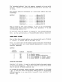
1
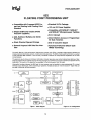
SYSTEM
(OmpuPro®_ _ _ _ _S_U_P_P_O_R_T_1_
™
A GODBOUT COMPANY
Technical Manual
IEEE 696/S/100
• INTERRUPT CONTROLLEI3S
• MATH PROCESSOR
• RS232 SERIAL CHANNEL
• INTERVAL TIMERS
• 4K RAM/ROM
• REAL TIME CLOCK/CALENDAR
$20.00
A189
SYSTEM SUPPORT 1 TECHNICAL MANUAL
Copyright 1981 CompuPro
Hayward, CA 94545
Document 1111620
File Name: SMORGY1.MAN
Board No. 162, Revision G
First Printing:
Latest Printing:
July 1981
December 1983
DISCLAIMER - CompuPro makes no representations or warranties with
respect to the contents hereof and specifically disclaims any
implied warranties of merchantability or fitness for any particular
purpose. Further, CompuPro reserves the right to revise this
publication and to make any changes from time to time in the
content hereof without obligation of CompuPro to notify any person
of such revision or changes.
Registered trademarks: CompuPro, CompuPro.
Trademark: System Support 1, CompuPro.
"8086 FAMILY USER'S MANUAL" October 1979, pages A137 through A157,
Copyright 1979, Intel Corporation. "PERIPHERAL DESIGN HANDBOOK"
August 1980, pages 1-61 through 1-68,
Copyright 1980, Intel
Corporation. "COMPONENT DATA CATALOG" January 1981, pages 8-21
through 8-26, and pages 8-31 through 8-38, Copyright 1981, Intel
Corporation. Reprinted by permission of Intel Corporation.
All rights reserved. No part of this publication may be reproduced
or transmitted in any form, or by any means, without the written
permission of CompuPro.
Printed and assembled in the United
States of America.
CONTENTS
HOW TO CONFIGURE YOUR SYSTEM SUPPORT 1 IN UNDER 5 MINUTES,
WITHOUT READING THE MANUAL • • • • •
• • • •
Other options and jumpers • • • •
Important note about system memory • •
1
2
3
TECHNICAL MANUAL
About System Support 1 •
Technical overview •
4
4
4
CONFIGURING THE SYSTEM SUPPORT 1
Setting I/O address
• • • • •
Setting memory address • • • • • •
Other memory options • •
• • •
Disabling the memory • • • • • • •
Global/extended address selection
Phantom* response options
Battery back-up for CMOS RAM • • •
Wait states • • • • • • • • • • •
Using higher speed 9511A or 9512 •
Interrupt jumpers and options
Using a 9511 or 9512 with interrupts
Interval timer options • • • • • • •
Configuring the serial channel • • •
Other miscellaneous hardware options
Connecting the battery • • • • • • •
Mounting the battery holder
Replacing the battery
• • • •
I/O port map • • • • • • • • •
• •
7
7
8
9
9
10
10
10
11
11
12
14
14
• • • • •
• •
• •
PROGRAMMING CONSIDERATIONS FOR THE SYSTEM SUPPORT 1 •
Power-up initialization
Programming the serial channel •
UART initialization •• • • • •
Sample UART program • • • • •
Programming the real time clock • • • •
Clock programming sequence • • •
Sample clock program • • • • • •
Programming the interrupt controllers
Important note about using DDT to debug interrupts •
"INTEL 8259A Programmable Interrupt Controller" ••
Initializing the 8259A • • • • • • • • • • •
Routine for initializing master/slave 8259As •
Disabling the 8259As • • • • • • • • • • • • •
15
16
18
18
18
19
20
20
20
26
26
27
29
30
38
39
40
60
60
61
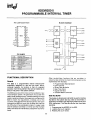
Programming the interval timer •
"INTEL 8253/8253-5 Programmable Interval Timer".
Programming the 9511 or 9512 math processor
"INTEL 8231 Arithmetic Processing Unit"
"INTEL 8232 Floating Point Processing Unit"
THEORY OF OPERATION
Address decode •
ROM/RAM circuitry
Interrupt controllers
Interval timer •
Serial channel •
Math chip
Real-time clock/calendar •
Power-fail driver
Wait state generator •
Data bus •
HARDWARE SECTION
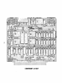
Parts list •
Component layout •
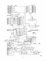
Logic diagram
INDEX.
CUSTOMER SERVICE/LIMITED WARRANTY INFORMATION
62
63
70
73
79
87
87
88
89
90
91
91
92
93
93
94
95
95
96
97
100
• back page
HOW TO CONFIGURE YOUR SYSTEM SUPPORT 1
IN UNDER 5 MINUTES, WITHOUT READING THE MANUAL
This section is for those of your that can't wait long enough to
read the manual to find out if your System Support 1 board works.
WE STRONGLY RECOMMEND THAT YOU RELAX, AND READ THE MANUAL!!!
If,
after reading and following the directions--rtlthis section, your
board appears not to function, DON'T CALL!!!
READ THE MANUAL
FIRST!!!
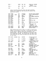
SWITCHES
DIP SWITCH I - is located near the right hand edge of the PC board
and is used to select the number of wait states, and various memory
options.
Position
I
2
3
4
Labeled
W8
W4
W2
WI
5
RDI
6
XA
7
8
PHD
PHE
How to Set It
OFF
OFF
OFF
ON if you have a 4 MHz or
greater CPU, otherwise, OFF.
OFF if you are using the RAM/ROM,
ON otherwise.
ON if you are not 'using extended
addressing, OFF otherwise.
ON
OFF
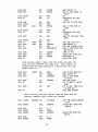
DIP SWITCH 2 - is located between U32 and U33 and is used to set
the extended address that the ROM/RAM responds to. If you are not
using extended addressing or the ROM/RAM then turn all switch
positions of Dip Switch 2 OFF. Otherwise they are set according to
the following table:
Position
I
2
3
4
5
6
··
··
··
7
8
·
·
Address Bit
A23
A22
A21
A20
Al9
Al8
Al7
Al6
. . ··
·
·
ON
=
"0"
OFF = "1 "
··
DIP SWITCH 3 - is located between U35 and U36 and is used to set
the address of the I/O ports and the ROM/RAM. Positions I through
4 are used to set the ROM/RAM address. If you are not using the
ROM/RAM then turn positions I through 4 OFF. If you are using the
ROM/RAM then they are set according to the following table:
I
Position
1 • •
2
3
4 •
Address Bit
• A15
• A14
• A13
• • • • • A12
ON = "0"
OFF = "1"
Positions 5 through 8 are used to set the address of the I/O ports.
To set them for the CompuPro standard (block of ports at 50 hex)
then set the switches as shown in the following table:
How to Set It
Position
5
• • • • • • ON
6 • • . • • • • • • OFF
7 • .
• • ON
8 •
• • OFF
OTHER OPTIONS AND. JUHPERS
Insert a dip shunt in locations J2 and J8. J2 is located at the
top of the board between the serial connector and U2. J8 is located
at the bottom left-hand side of the board between U30 and U31.
Connect the battery cable by plugging it onto J3 (which is located
near the top right-hand side of the board just to the right of the
regulator). The connector is polarized but make sure the red wire
is towards the left.
If you are using the System Support 1 with our CPU 8085/88 board or
any ~ther 8085/8088/8086 type board, then install the shorting plug
at jumper J13 so that the pins labeled "8" and .. c.. are connected
together (shorting plug will be left of center).
If you are using a CPU 8086, CPU 68K or any other 16-bit CPU with
your System Support 1, make sure you change the Sys tem Support 1
board as described below.
1)
Carefully pull IC U28 from its socket. (IC U28 is
located on the right hand side of the board.)
2)
Bend out pin 4 so that when the IC is replaced, pin 4
will not make contact with the socket or anything else.
3)
Replace IC U28 in its socket and verify that every pin
except pin 4 is back in its hole.
If you are using the System Support 1 wi th our CPU Z or any other
Z-80 or 8080 type CPU board (like an old IMSAI CPU), then install
the shorting plug at jumper J13 so that the pins labeled .. z" and
.. c.. are connected together (shorting plug will be right of center).
J13 is located at the bottom right hand corner of the PC board.
2
IMPORTANT NOTE ABOUT SYSTEM MEMORY
When using the System Support 1 with its on-board interrupt
controllers, and you are using an 8080 or Z-80 CPU, it is important
that all your system memory respond (become disabled) to the 5-100
PHANTOM* signal which is on bus pin 67.
Therefore you must
configure all your system memory to respond to PHANTOM*.
3
TECHNICAL MANUAL.
ABOUT THE SYSTEM SUPPORT 1
Congratulations on your purchase of the System Support 1 board - a
multi-function··module designed specifically for full electrical and
mechanical compatibility with the IEEE 696/S-100 Bus standard. The
S-100 bus is the professional level choice for commercial,
industrial and scientific applications. This bus provides for
ready expansion and modification as the state of the art improves.
We believe that this board, along with the rest of the CompuPro
family, is one of the best boards available for the S-100 Bus.
The System Support 1 board combines many of the most often desired
"extras" in an S-100 computer system. Most of these features don. . t
take up enough board space to justify an entire board devoted to
performing specifically that function. For example, if every
function that is performed by the System Support were put on a
separate board, it would take up 7 slots! By integrating all these
functions into one multi-function board, we have conserved slots,
power, and cost.
This board provides the system with sophisticated control of bus
interrupts, 3 independent interval timers, a "real time" clock/calendar that provides BCD hours/minutes/seconds /month/day/year
with battery backup, a full RS-232 serial channel which includes
full handshaking, space for 4K of RAM or EPROM with provision for
battery back-up for 2K of CMOS RAM, provision for adding a high
performance math processor to increase system throughput, and
generation of the new S-100 signal PWRFAIL*.
TECHNICAL OVERVIEW
The System Support 1 provides the system with the following
functions:
(1)
Two sophisticated LSI interrupt controllers. These handle the
eight vectored interrupts from the S-100 Bus, as well as 7
interrupts generated on-board. Thus, the on-board interrupt
sources do not use up any of the S-100 bus interrupt pins.
The interrupt controllers provide sophisticated control of
interrupt. . s priority, fully independent masking, and vectors
to a service routine table that may be located virtually
anywhere in memory. The interrupt controllers can function in
an 8080/8085/Z-80 environment, as well as the 8088/86
environment.
(2)
Three independent interval timers. These are 16 bit counters
that can be written to, read from, and can cause interrupts.
They are clocked by a 2 MHz source, but provision has been
made to allow external clock inputs, or the counters may be
4
cascaded for longer counts. A gate input is provided for each
counter to allow timing of external events. The counters can
operate in one of six modes: Interrupt on Terminal Count,
Programmable One-Shot, Rate Generator, Square Wave Generator,
Software Triggered Strobe and Hardware Triggered Strobe.:
(3)
A full RS-232 serial channel. This serial channel provides
features like: Full modem and handshaking control lines,
master/slave jumper options, fully software programmable UART
features such as parity, word length and baud rate, and provision to run in an interrupt driven mode. The baud rates are
crystal controlled.
(4)
A real time clock/calendar with battery back-up. Our real time
clock keeps "real time"; hours, minutes etc. Our clock is not
just an interrupt every few milliseconds that requires
processor overhead to actually keep track of the time and
date. (But you could use the interval timers to do that!)
Included are features like 12 or 24 hour format, hour/minute/second /month/day/year/day-of-week indication, individually
accessible digits, BCD format, battery back-up with a battery
life of more than one year, and crystal controlled time-base.
(5)
Sockets for 4K of RAM or EPROM. You can use two 2716 type
EPROMs or two of the new "byte-wide" RAMs or one of each.
Provision is made to power one of the sockets from the clock
battery if desired for use with the Hitachi 6116 CMOS RAM
chip. The power consumption from the battery is so low that
the data will be retained for over one year, and that includes
running the clock. The memory space is addressable on any 4K
boundary via a dip-switch, and may also respond to the full 24
bits of IEEE extended addressing. The extended address is
also selectable by a dip-switch. The memory may also respond
to the PHANTOM* signal; it may appear or disappear when
PHANTOM* is asserted. The PHANTOM* polarity is selected by a
dip-switch. The memory may be disabled with a dip-switch.
(6)
A socket for a 9511A or 9512 LSI math processor. This chip is
not provided with the standard board since the price/performance tradeoff may not be justified in all systems. But if you
really need the higher system throughput, the chips are
available from us, or you may add your own. In any case, the
capability for later expansion is provided, should your need
arise.
Provision has been made for either math chip, whichever you prefer. The math chip can run in an interrupt driven
mode, which allows the math functions to occur in parallel
with other processing on the bus.
The math chips currently
run at 2 MHz, but provision has been made for an on-board
crystal oscillator so that you can use the faster versions of
these chips.
Buying a math processor all by itself on a
separate S-100 board usually costs more than the price of an
entire System Support 1.
(7)
Implementation of the S-100 Bus Signal PWRFAIL*. This signal
does not meet the exact spec as defined by the new IEEE 696/S5
100 Standard, but is asserted well before the regulators drop
out of regulation.
This allows thousands of instructions to
be executed before the system crashes. Couple this with the
battery back-up RAM capability and now you have a useful
power-fail system that will allow you to recover in an orderly
fashion. Provision is made on-board to jumper the PWRFAIL*
line to the NMI* line.
(8)
The System Support 1 takes up a block of 16 I/O ports and is
addressable on any 16 port boundary. Provision is made to
generate one, two, four or eight wait states to insure
operation with the fastest of processors.
This board was
designed for full compliance with the IEEE 696/S-100 specifications to insure complete compatibility for today and the
future.
For a more complete discussion of the actual implementation of
these features, refer to the Theory Of Operation section of this
manual.
By now you can see that the System Support 1 is the perfect
addition to any S-100 system, but when coupled with one of our
CPUs, can make a complete system with just two boards! Many long
hours of thought and revision went into this product, and we at
CompuPro are confident that it will provide years of solid
service. We sincerely hope that you will enjoy it.
6
CONFlGURIRG THE SYSTEM SUPPORT 1
The System Support 1 occupies a group of 16 I/O ports, and 4K of
memory space, if the memory is to be used. The I/O ports can
reside on any 16 port boundary and the memory on any 4K byte
boundary. Both addresses are set with Switch 3.
Switch 3 is located in between U35 and U36 in the lower row of
chips and is marked "ROM/I/O ADDR".
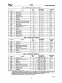
SETTING THE I/O ADDRESS
The I/O address is set by Switch 3, positions 5 through 8.
switch position corresponds to a particular address bit:
SWITCH 3
Position
Position
Position
Position
5 •
6 • •
7
8 • •
Address
Address
• Address
Address
Bit
Bit
Bit
Bit
Each
7
6
5
4
When a switch is "ON", that matches a "0" bit on the corresponding
address line. When a switch is "OFF", that matches a "I" bit on
the corresponding address line.
The following table shows all possible I/O addresses that the
System Support 1 can reside at, and the associated switch settings.
SWITCH 3
Switch Position
I/O Address
00 (hex)
10
20
30
40
SO
60
70
80
90
AO
BO
CO
DO
EO
FO
6
5
-ON· · · -ON-
-ON-ON-ON-ON-OFF-OFF-OFF-OFF
-ON-ON-ON-ON-OFF-OFF-OFF-OFF-
·
-ON·
-ON·
-ON·
· -ON·
· · -ON· · · · -ON·
-OFF· . . · · -OFF· · · · -OFF··
-OFF-OFF·
·
· -OFF· · -OFF.
-OFF·
7
-ON-ON-OFF-OFF-ON-ON-OFF-OFF-ON-ON-OFF-OFF-ON-ON-OFF-OFF-
8
-ON-OFF-ON-OFF-ON-OFF-ON-OFF-ON-OFF-ON-OFF-ON-OFF-ON-OFF-
The "standard" port block that we have assigned to the System
Support 1 is the block at SO hex. All of the software provided by
CompuPro and other vendors will assume that you have the board
addressed to this block. To set the System Support 1 to block SO
hex, set switch positions 5=ON, 6=OFF, 7=ON, and 8=OFF.
7
SETTING THE MEMORY ADDRESS
The System Support 1 has a 4K block of EPROM or RAM. This memory
may reside at any 4K byte boundary in the system. The address of
the block is set by two switches: part of Switch 3 and all of
Switch 2. Switch 3 is used to set which block in the 64K "page"
that the memory uses, and Switch 2 is used to select which of the
256 possible 64K "pages" (corresponding to the new address lines
A16-23) is to be used.
The 4K block address within the 64K page is set by Switch 3,
positions 1 through 4. Switch 3 is located in between U35 and U36
in the lower row of chips and is marked "ROM/I/O ADDR".
Each of the four switch positions correspond to a particular
address bit:
SWITCH 3
Position
Position
Position
Position
1
2
3
4
•
•
•
•
• Address Bit
• Address Bit
Address Bit
• Address Bit
15
14
13
12
When a switch is "ON", that matches a "0" bit on the corresponding
address line. When a switch is "OFF", that matches a "I" bit on
the corresponding address line.
The following table shows all possible 4K byte boundaries that the
memory may start at, and the associated switch settings:
SWITCH 3
Memory Address
0000 (hex)
1000
2000
·3000
4000
5000
6000
7000
8000
9000
AOOO
BOOO
COOO
DOOO
EOOO
FOOO
·
·
·
··
·.
·
·
·
·
·
·
·
·
·
Switch Position
2
3
1
· · -ON-ON-
-ON-ON-ON-ON-OFF-OFF-OFF-OFF
-ON-ON-ON-ON-OFF-OFF-OFF-OFF-
·
· · -ON· -ON· -ON-ON· · -ON· · -ON·
· -OFF· · -OFF· ·· -OFF-OFF· · -OFF· -OFF-OFF· -OFF·
-ON-ON-OFF-OFF-ON-ON-OFF-OFF-ON-ON-OFF-OFF-ON-ON-OFF-OFF-
4
-ON-OFF-ON-OFF-ON-OFF-ON-OFF-ON-OFF-ON-OFF-ON-OFF-ON-OFF-
U16 occupies the upper 2K of the 4K address space and U17
occupies the lower 2K of address space. For example, if the memory
were addressed at FOOO hex then U17 would reside at FOOO to F7FF
and U16 would reside at F800 to FFFF.
ROTE:
8
The "extended address" that the memory responds to is set with
Switch 2. Switch 2 is located between U32 and U33 in the lower row
of chips.
Each switch position corresponds to a particular address bit (see
following) :
SWITCH 2
Position
Position
Position
Position
Position
Position
Position
Position
1
2
3
4
5
6
7
8
·
··
·
·
·· .
··
• Address
Address
Address
Address
Address
Address
Address
Address
·····
·
·
·····
. · · · ·· ··
·····
Bit
Bit
Bit
Bit
Bit
Bit
Bit
Bit
23
22
21
20
19
18
17
16
When a switch is "ON", that matches a "0" bit on the corresponding
address line. When a switch is "OFF", that matches a "I" on the
corresponding address line.
If you don't want the memory to respond to the extended address
bits, see the section below on "Global/Extended Address Selection".
0TIIKll MEMORY OPTIONS
Most of the other memory options are selected with part of Switch
1. Switch 1 is located just to the right of U22.
First is a quick chart of the memory options associated with Switch
1, then we will give you a more detailed description of each of the
swi tch's functions.
SWITCH 1
Switch
Position
Labeled
Function
5
RDI
6
7
XA
8
PRE
ON
ON
ON
ON
PHD
to
to
to
to
disable memory.
disable extended addressing.
allow PHANTOM* to disable memory.
allow PHANTOM* to enable memory.
DISABLING THE MEMORY
Position 5 of Switch 1 is used to entirely disable the memory space
on the System Support 1. This will mainly be used if you don't
wish to use anyon-board memory at all.
To disable the on-board memory entirely, turn position 5 of Switch
ION. If you don't wan t the on-board memory space to be disabled
(if you're going to use some kind of memory), turn position 5 of
Switch 1 OFF.
9
GLOBAL/EXTENDED ADDRESS SELECTION
Position 6 of Switch 1 is used to determine whether or not the
memory responds to the lower 16 address bits and ignores the upper
8 address bits, or responds to the entire 24 address bits.
When the memory ignores the upper 8 address bits, it will appear in
each 64K page. This is called "global" memory.
If you have a
processor card that is only capable of generating 16 address bits,
then you will want to use the memory as global.
If you want the memory to respond to the full 24 address bits, turn
position 6 of switch 1 OFF. If you want the memory to be global,
then turn position 6 of Switch 1 ON.
Note that if you want the memory to respond to the extended
address, you will have to set Switch 2 to the proper extended
address. See the above section "Setting the Memory Address" for
information on how to set Switch 2.
PHANTOM* RESPONSE OPTIONS
Positions 7 and 8 are used to determine how the memory on the
System Support 1 responds to the S-100 Bus signal PHANTOM*. The
memory can respond in one of three ways when PHANTOM* is asserted
on the bus. The memory may ignore the PHANTOM* signal entirely,
may become disabled or may become enabled.
If you want the memory to ignore the PHANTOM* signal, leave both
position 7 and position 8 of Switch 1 OFF.
If you want the memory to become disabled (disappear) when PHANTOM*
is asserted, then turn position 7 ON and position 8 OFF. This is
the most often desired setting.
-If'you want the memory to be enabled only when PHANTOM* is
asserted, then turn position 7 OFF and position 8 ON.
NEVER turn both positions 7 and 8 ON at the same time!
BATTERY BACK-UP FOR CMOS RAM
We provide two HM6116 RAM chips already installed in locations U16
and Ul7. The RAM chip at U17, which appears as the lower 2K in the
4K address space, will be "battery backed-up" if you have installed
the external battery as outlined in section (Connecting the
Battery).
This means that any data written to this RAM chip will
be retained when power to the computer is turned off, as long as
the battery remains connected.
If you ever decide to use an EPROM in that socket, be sure to
remove diode D3, otherwise the clock battery will be drained
excessively (and who needs to battery back-up an EPROM?).
10
WAIT STATES
The System Support 1 has circuitry that enables it to generate one,
two, four or eight wait states. This will mostly be used in
systems where the processor is running at a very high speed. In
this industry it has always been the case that the speed of the CPU
chips increases years before the speed of the LSI peripheral chips.
Since the System Support 1 makes extensive use of these LSI
peripheral chips, it may be necessary to add wait states to all
accesses made to the board.
Part of Switch S1 is used to add wait states to all accesses made
to the board. S 1 is loca ted just to the right of U22 at the right
hand edge of the board. Positions 1 through 4 of S1 are used to
select the number of wait states to be generated according to the
following table:
Number of
Wait States
None
1
2
4
8
(W8)
-OFF-OFF-OFF-OFF-ON-
Switch Position
2(W4)
3(W2)
4(W1)
-OFF-OFF-ON-ON-ON-
-OFF-ON-ON-ON-ON-
-OFF-OFF-OFF-ON-ON-
NOTE: These wait states affect the entire board, I/O ports and
memory accesses.
USING A HIGHER SPEED 951LA OR 9512
As supplied, the System Support 1 is designed to use either a 9511A
or 9512 math processor chip running at 2 MHz. This is the lowest
cos t version of these chips. The 2 MHz clock is taken from S-100
Bus pin 49 which is specified by the S-100 Standard to be a 2 MHz
clock signal.
But we have made a provision for using an on-board crystal oscillator instead of the 2 MHz signal from the S-100 Bus. This was done
primarily for two reasons:
1.
Some users may desire to use the higher speed (3 and 4 MHz)
versions of the 9511A or 9512.
2.
Some of the older S-100 systems may not have the 2 MHz clock
signal available on pin 49.
If your requirements fit any of the above, then you will want to
install the extra crystal required for the on-board oscillator.
This is crystal Xl and is located just to the right of
left-hand edge of the board. Note that this crystal
twice the frequency that you require. If you are using
speed 9511A or 9512 (2 MHz) but there is no 2 MHz clock
11
U11 at the
should be
a standard
on pin 49,
then Xl should be a 4 MHz crystal. If you are using a 3 MHz 9511A
or 9512 then Xl should be 6 MHz. If you are using a 4 MHz version
then Xl should be 8 MHz.
A proper crystal is available from
CompuPro. Be sure to specify a frequency of twice the operating
speed of your math chip.
You will also need to install a jumper at location J5 (located
upwards and to the right of Xl) and also cut a trace at J5. If you
are using the on-board oscillator option, then you must cut the
trace connecting the two pads in the "B" block of J5. This trace
is located on the back (solder) side of the PC board. Use an XACTO
knife and be extremely careful not to damage any other traces.
Then you will need to install a jumper between the two pads in the
"A" block of J5.
If you are not using a higher speed 9511A or 9512, or you have 2MHz
on pin 49 in your system, or if you are not using a math processor
at all, then do nothing with J5 or install no crystal at Xl.
INTERRUPT JUMPERS AND OPTIONS
IMPORTANT NOTE ABOUT USING THE ON-BOARD INTERRUPT CONTROLLERS: The
System Support l's interrupt system has been designed to work with
8080/8085/Z-80/8088 CPUs. In order to account for an idiosyncracy
in the 8080 and Z-80 CPUs, the interrupt circuitry asserts the S100 bus signal PHANTOM* which is on bus pin 67. Therefore it is
necessary to configure all your system memory to be disabled when
PHANTOM* is asserted (if you are using a Z-80 or 8080 CPU). For a
discussion about why this is necessary, see the Theory of Operation
section of this manual. Note that the memory on the System Support
1 will always be disabled when the interrupt circui try requires,
regardless of how you have set the PHD and PRE switches.
is located at the lower right hand corner of the PC
board, and it is used to select how the System Support 1 treats
interrupt acknowledge cycles depending on what type of CPU you are
running.
JUMPER J13 -
If you are using the System Support 1 with our CPU 8085/88 board or
any other 8085/8088/8086 type board, then install the shorting plug
at J13 so that the pins labeled "8" and "c" are connected together
(shorting plug is left of center).
If you are using the System Support 1 wi th our CPU Z or any other
Z-80 or 8080 type of CPU (such as an old IMSAI CPU), then install
the shorting plug at J13 so that the pins labeled "z" and "c" are
connected together (shorting plug is right of center).
The interrupt structure of the System Support 1 has been designed
to be both easy to use and at the same time very flexible. There
are two interrupt controllers on the board; one is the "master" and
the other is the "slave". The two interrupt controllers look at 15
different interrupt sources. Eight of these come from the S-100
12
Vectored Interrupt lines and seven interrupts may be generated from
various sources on the board itself.
In general, the master interrupt controller. . s "interrupt request"
inputs have a higher priority than those of the slave interrupt
controller. The master looks at seven of the 5-100 Bus Vectored
Interrupts (VIO-6*) and the slave looks at the eighth vectored
interrupt and seven interrupt sources that are generated on the
System Support 1.
This is the "standard" configuration, but
through the use of dip headers and jumpers, almost any configuration is possible. For example, if an interrupt controller already
exists in your system, the on-board interrupts may be jumpered to
any of the S-100 vectored interrupt lines. This means that the
interrupting capability of the various board functions are not lost
even though you are not using the on-board interrupt controllers.
Or some interrupts may be handled on board and some off board, or
an on-board interrupt may be given a higher priority by jumpering
it to an S-100 interrupt line which is responded to by the master.
To allow the System Support 1 to be easily configured, a "standard"
set of interrupt assignments may be selected by merely plugging in
a dip-shunt in one location, (J8), and leaving J7 open.
If you
don. . t want a standard configuration, you may custom program these
jumper areas with dip-headers instead of the shunts. If the shunt
is plugged into location J8 and location J7 is left open then the
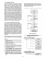
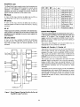
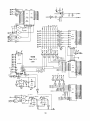
board. . s interrupt configuration, (see the following figure):
VIO*
VIl*
VI2*
VI3*
VI4*
VI5*
VI6*
VI7*
S-100
Vectored
Interrupts
>------IIRQ
>------IIRQ
>------IIRQ
>------IIRQ
>------1 IRQ
>------IIRQ
>------IIRQ
>--1 I-IIRQ
0
1
2
3
4
5
6
7
INT 1---->S-100 INT* line.
1
1
1
8259A MASTER
(UI5)
1
1
1
1
1 1 ----------------
1 1
On-Board
Interrupts
1 1-------1
1
(----slave interrupt output
----------------
I---IIRQO
TIMERO OUT>------IIRQl
TIMERI OUT>------IIRQ2
TIMER2 OUT>------IIRQ3
9511 SVRQ >------IIRQ4
9511 END >------IIRQ5
2651 TxRDy>------IIRQ6
2651 RxRDy>------IIRQ7
1
8259A SLAVE
(UI4)
If you wish to "scramble-wire" the interrupts, all interrupt
sources and destinations appear at jumpers J7 and J8. They may be
jumpered in any conceivable configuration by using dip-headers.
The interrupts appear at these jumpers as shown in the following
diagrams:
13
Destinations
Sources
J7
9512 ERROR>------116
9511 END >------115
9511 SVRQ >------114
TIMER2 OUT>------113
TIMER1 OUT>------112
TIMERO OUT>------111
2651 TxRDy>------110
2651 RxRDy>------19
11----->S-100
21----->S-100
31----->S-100
41----->S-100
51----->S-100
61----->S-100
71----->S-100
81----->S-100
VI7*
VI6*
VI5*
VI4*
VI3*
VI2*
Vl1*
VIO*
91----->SLAVE
101----->SLAVE
111----->SLAVE
121----->SLAVE
131----->SLAVE
141----->SLAVE
151----->SLAVE
161----->SLAVE
IRQO
IRQ1
IRQ2
IRQ3
IRQ4
IRQ5
IRQ6
IRQ7
J8
S-100 VI7*>------18
TIMERO OUT>------17
TIMER1 OUT>------16
TlMER2 OUT>------15
9512 SVRQ >------14
9512 END >------13
2651 TxRDy>------12
2651 RxRDy>------11
USING A 9511 OR 9512 WITH llITERRUPTS
The "END" interrupt from the 9511 or 9512 is not actually connected
directly to J7 and J8 as is shown above. This is because the
polarity of the END signal is different between the 9511 and the
9512.
J6 is used to select the appropriate polarity for this
signal depending on which math processor you are using.
If you are using a 9511A then install a jumper in the "A" block at
J6. If you are using a 9512 then install a jumper in the "B" block
at J6.
If you are using either math chip but are not running it "interrupt
driven", then you do not need to install any jumper at J6.
Also note that the "ERROR" output from the 9512 (9511A does not
have this output) is not available at both J7 and J8 as the other
math chip outputs are. The ERROR signal is only available at J7.
INTERVAL TIMER OPTIONS
The three interval timers on the System Support 1 are implemented
with an 8253 IC. It contains three independent timer sections.
Each section has a clock input, gate input and timer output. These
9 inputs and outputs appear at J4 so that the different sections
may be cascaded for longer time delays or so that the signals may
14
l
'be connected to ex:ternal devices'.
connections at J4:
The following diagram shows the
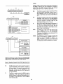
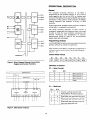
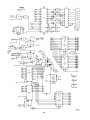
J4
! '':''--'--~'-----
INVERTED TIMER 0 OUTPUT<---2:"ll'; 16-----------)TIMER 0 OUTPUT
INVERTED TIMER 1 OUTPUT<---~-.r2
"',IS I-----------)TIMER 1 OUTPUT
INVERTED TIMER 2 OUTPUT< ---.:~ 13
~:141----------- )TIMER 2 OUTPUT
TIMER 0 CLOCK INPUT)---------14-~--~~131-------------<2 MHz SOURCE
TIMER 1 CLOCK INPUT>-------70-::-15'----.:..~ 121-------------<2 MHz SOURCE
TIMER 2 CLOCK INPUT)-------~-16-----~III-------------<2 MHz SOURCE
TIMER 0 GATE INPUT)---------.:..'17
' 101-------------NO CONNECTION
TIMER 1 GATE INPUT)----------18
91-------<TIMER 2 GATE INPUT
I
NOTES: All gate inputs are pulled up with a 4.7K ohm resistor.
Pins 4 and 13 are connected together, pins 5 and 12 are connected
together and pins 6 and 11 are connected together. All timer
outputs are buffered.
To cascade sections or use extern'al clocks, the appropriate
trace(s) must be cut on the solder side 'of the. board to remove the
2 MHz clock sou~c~; Then the output of another se~tion or an
external inpuimay be connected ib the clock inputs (TTL ONLY!).
'
,
Use a dip header to make the interconnections.
CONFIGURING THE SERIAL ClIANHEL
The Serial Channel on the System Support 1 has been designed to be
as flexible as possible. It may be used in the "master" or "slave"
mode and provides full RS-232C handshaking lines. A standard 26
pin transitio~ ~onrie~t~r h~s been provided at Jl to facilitate easy
connection of a ribbon ~able that usually ~as a DB-25 style
conn'ector on the other end. Such a cable is' available from us or
your CompuPro d~aler.
All of the serial signals appear ~t J2 w.hich allow them to be wired
as either a master or slave device. An example of a master device
would be a terminal or printer and an example of a slave device
would be a modem or other computer. Therefore, the serial channel
must be configured to compienientth~ device it is connected to. In
other words, if y~u are 'using th~ serial channel with a terminal (a
master device) then you will want to configure the serial channel
to act as a slave. Conversely, if you are using the serial channel
with a modem (a slave device) then you will want to configure the
serial channel to act as a master. ,
Since the most common configuration will be that of a slave, we
hav~'~ade it ~asy for ydu to ins~~il this configuration.
This may
be accomplishe,d'me'rely by ins'talling dip-shunt in location J2.
A~ain, you ~il~; wan~ t6-us~ this configura~ion if you ~re hooking
up the serial channel to a standard te,rminal or printer.
a
IS
To configure the serial channel to act as a master, then you will
need to cross-wire J2 by using a dip-header. This configuration is
shown in the following diagram:
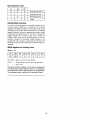
J2
For reference purposes, the signals appearing at J2 and Jl are as
follows:
'J2
Jl
TxD)------11
161------13
RxD<------12
151------12
RTS)------13
141------15
26 Pin Transition Connector
CTS<------14
131------14 I
and 25 Pin DB-25 Connector
DSR<------15
121------1201
DTR)------16
111------16 I
DCD<------17
101------18 I
+12V------18
91--1
11 I------GND
--------- I
17 I------GND
I
-12V-----------------1
TxD = Transmitted Data
RTS
Request To Send
DSR = Data Set Ready
DCD = Data Carrier Detect
RxD
CTS
DTR
GND
= Received Data
= Clear
To Send
= Data Terminal Ready
= Ground
DIAGRAM OF J2-JI-SERIAL SIGNAL RELATIONSHIPS
Setting the baud rate, stop bits, parity and other UART parameters
is done in software and will be covered in a later section called
"Programming The Serial Channel".
OTHER MISCELLANEOUS BABDVARE OPrIOBS
Use of pSTVAL* - The System Support 1 uses the new S-100 Signal
pSTVAL* that appears on S-100 Bus pin 25.
If you are using a CPU
from CompuPro (or any other CPU that meets the IEEE/696 standard),
then this signal will be generated by the CPU. and you need not
worry about this next jumper.
16
If you are using an older generation CPU board that does not
generate pSTVAL*, then you will need to make a small modification
to the System Support 1. Proceed as follows:
Locate Jll. It is located near the edge connector in approximately
the center of the board. Jll has three pads labeled A, C and B.
If you look on the back (solder) side of the board you will notice
that there is a small trace connecting pad B to pad C. Using an
XACTO knife, carefully cut this trace. Take care not to damage any
other traces on the PC board. Then install a jumper between pads A
and C. That completes this modification.
Use of SLAVE CLR* Instead of RESET* - The S-100 signal SLAVE CLR*
(bus pin 54) is specifically designated for clearing slave devices
(the System Support 1 is a slave device). However, it is usually
more convenient in most systems to use RESET* instead of SLAVE
CLR*. The System Support 1 is currently wired to use RESET* to
clear the various circuits on the board. Provision has been made
to use SLAVE CLR* instead of RESET* if you so desire.
To do this, locate J9 and J12. J9 is a single jumper pad located
at the bottom left-hand corner of the board just above the edge
connector fingers. J12 is also located at the bottom of the board
just above the edge connector fingers, but near the center of the
board. J12 has two pads that are connected together by a trace on
the back (solder) side of the board. This trace must be cut with
an XACTO knife. Be sure not to damage any other traces. Then,
using a length of insulated wire (such as wire-wrap wire), install
a jumper between the pad of J9 and the left-most pad of J12 (the
one closest to the "C"). This will cause the circuitry on the
board to be cleared in response to POC* and SLAVE CLR*.
PWRFAIL* and NMI* - The System Support 1 generates the S-100
PWRFAIL* signal which is used to indicate that a loss of power is
imminent.
You will usually want this signal to cause a nonmaskable interrupt (NMI*) to the CPU. The CPU can then save any
data it deems relevant. Provision has been made to jumper the
PWRFAIL* signal to the NMI* line on the S-100 Bus. Thus both
PWRFAIL* and NMI* would be asserted low about 15 milliseconds
before the regulators in the system drift out of regulation. (The
exact time will depend on your system's power supply and loading.)
If you desire to have the PWRFAIL* signal cause an NMI*, then
install a jumper at location JI0. JI0 is located at the bottom
left hand side of the board, just above the edge connector fingers.
If you don't care about the PWRFAIL* signal, then you need not do
anything with JI0.
As an option, the PWRFAIL* signal is available at the right-most
pad of JI0. It could conceivably be hooked to any other S-100
interrupt pin via a header at J7. It should be mentioned, however,
that this would not be a good practice because any of the other
interrupts could be "masked" at the time of power failure, thus
defeating the purpose of the PWRFAIL* signal.
17
CONNECTING THE BATTERY
The battery connector supplied with the System Support 1 is semipolarized so that it should only plug onto J3 easily in one
direc tion. To double check, the red wire which connec ts to the +
side of the battery should correspond to the + marking on the
board.
If'you desire to use a different battery than the one supplied (for
example three 1.5 volt penlight cells in series for longer battery
life) then you should take care to keep the polarities correct.
The circuitry on the System Support 1 is protected from reverse
polarity so no damage will occur if the battery is reversed, but
the board won't function properly.
The battery is shipped already plugged into its holder, but should
it become necessary to remove it, be sure to orient the + end of
the battery to correspond to the + stamped in battery holder.
MOUNTING THE BATTERY HOLDER
The battery holder is intended to be mounted outside the computer
enclosure. This is because batteries, although sealed, under some
conditions can still leak, out gas or otherwise do nasty things to
the sensitive components and contacts inside your computer. Therefore, we strongly recommend that the battery be mounted outside the
computer enclosure and not inside.
REPLACIRG THE BATTHK.Y
The 4.5 volt alkaline battery that is supplied with the System
Support 1 should last approximately 1.5 years with normal use.
However, to insure that a loss of time or memory data does not
occur due to battery failure, we recommend that the battery be
replaced once every year. The battery can be replaced while the
system power is on, so that operation of the clock or memory data
will not be lost, (unless of course you get a power failure at the
exact instant that you remove the battery).
The type of battery used is a Mallory PX21 or Eveready 523.
Replacement batteries are available from us or possibly your local
dealer. You can probably also obtain this battery from a photo
store or possibly a "drug" store with a well stocked photo
department. This battery is also used in some smoke alarms, so you
may also find it in a well stocked hardware store.
If you plan to keep a replacement battery handy, be aware that the
average shelf life of an alkaline battery is two years. This can
be extended significantly by storing the battery in a refrigerator.
Before using a battery that has been stored in the refrigerator,
allow it to come up to room temperature and make sure that there is
no moisture present on any of the contacts.
18
*******************************************************************
IMPORTANT HOTE: Please do not use anything other than an alkaline
battery.
Mercury cells may seem like a good choice for this
application, but they do not fare too well under the light load
presented by the System Support 1. Carbon-Zinc cells can leak,
causing damage to the computer (usually irreparable). Ni-cads will
not be recharged by the board's circuitry. Also note that using any
battery other than the ones specified will void your warranty.
*******************************************************************
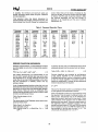
I/O PORT HAP
The System Support 1 uses a block of 16 I/O port addresses. This
block may begin at any 16 port boundary. Each of the I/O ports
performs a specific function and each will always appear at an
address that is relative to the base address.
The following chart
shows the I/O port's relative positions, and their actual address
when the System Support 1 is addressed to the block at SOH
(CompuPro standard address).
Port Function
Relative Position
Address
----------------------------------------------------------------Master 8259A lower port (AO=O)
Master '8259A upper port (AO=I)
Slave 8259A lower port (AO=O)
Slave 8259A upper port (AO=1)
Timer/Counter 0
Timer/Counter 1
Timer/Counter 2
Timer/Counter Control Register
9511A/9512 Data Port
9511A/9512 Command Port
Clock/Calendar Command Port
Clock/Calendar Data Port
2651 Data Register
2651 Status Register
2651 Mode Registers
2651 Command Register
19
Base+ 0
Base+ 1
Base+ 2
Base+ 3
Base+ 4
Base+ 5
Base+ 6
Base+ 7
Base+ 8
Base+ 9
Base+l0
Base+11
Base+12
Base+13
Base+14
Base+15
dec
dec
dec
dec
dec
dec
dec
dec
dec
dec
dec
dec
dec
dec
dec
dec
0 hex
50 hex
1
2
3
4
5
6
7
8
9
A
B
C
D
E
F
51
52
53
54
55
56
57
58
59
SA
5B
5C
5D
5E
SF
hex
hex
hex
hex
hex
hex
hex
hex
hex
hex
hex
hex
hex
hex
hex
hex
hex
hex
hex
hex
hex
hex
hex
hex
hex
hex
hex
hex
hex
hex
PROGRAHMING CONSIDERATIONS FOR THE SYSTEM SUPPORT 1
The following section of this manual will discuss some of the
software considerations that will be necessary to use this board.
We will provide you with a few actual programs, but these programs
are presented as either examples or for testing purposes and are
not necessarily the best way to do something. The listings were
prepared using the standard CP/M assembler (ASM.COM) and sometimes
assume a CP/M system (like for I/O calls).
First we will discuss the power-up initialization of the System
Support 1 and then we will discuss the programming considerations
for the various functions of the board.
POWER-UP INITIALIZATION
When you turn on your system, the first thing that usually happens
is to boot in the disk operating system or execute some kind of
program stored in ROM.
Somewhere at the beginning of these
programs is usually some code to initialize the system. This may
do things like set the stack pointer, clear some registers and send
a set of initial parameters to I/O peripherals.
This latter
example is what needs to be done with the System Support 1.
To be specific, the interrupt controllers must be set up with all
the data it takes to get th'em to respond correctly in your system
(like masking unused interrupts, setting priority levels, setting
the interrupt vector address etc.); the serial channel parameters
must be set (like the baud rate, word length etc.); the interval
timer modes must be set (if they are used) and so on.
How your board is to be set up on power-up is dependent solely on
your system requirements. Therefore, we will not attempt to give
every possible example of how the board may be initialized.
Instead, the following sections will discuss the various sections
of the System Support 1 in detail and you will have to derive the
initialization parameters from that data. The software examples
will all contain some kind of initialization routine, but they will
probably not be the same for your system.
P1lOG1lAMMING THE SERIAL CHANNEL
The serial channel on the System Support 1 is implemented with a
2651 type UART from either National Semiconductor or Signetics.
Several of the UART parameters and channel control functions are
programmed by writing into or reading from certain registers in the
2651.
20
They are:
1.
2.
3.
4.
S.
6.
7.
The baud rate.
The word length.
Whether or not a parity bit is generated.
Whether the parity is even or odd (if generated).
The number of stop bits.
Enabling and disabling the transmitter and receiver.
Setting and testing the RS-232 handshake lines.
In addition, the normal status indications and data transfer
functions are also handled through the UART's registers.
A table of the various registers and where they appear in the I/O
port map follows. (The port addresses assume that the System
Support 1 is set up to the CompuPro "standard" port block; see the
sections on setting the I/O address and the I/O port map for more
information.)
"READ" or "INPUT" Ports
Port Address
UART Register Function
SC
SD
SE
SF
Data Port, read received data word.
Status Port, read UART status info.
Mode Registers, read current UART mode.
Command Register, read current command.
hex
hex
hex
hex
"WRITE" or "OUTPUT" Ports
SC
SD
SE
SF
hex
hex
hex
hex
Data port, write word to be transmitted.
not used
Mode registers, write mode bytes.
Command register, write command to UART.
Data Registers
The UART data registers are straight-forward in their operation.
You write a byte to the data register when you want to transmit
that byte to an external serial device and you read the byte in the
data register to receive a byte from an external serial device. The
UART will automatically add the proper start and stop bits when
transmitting and will remove them when receiving.
Status Register
The status register is used to determine the current state of the
UART. Each bit of the status register has a different meaning
depending on whether it is high or low. (High means a logic one or
high level and low means a logic zero or low level.) The following
table describes the meaning of the status bits:
21
Bit
0 - TxRDY:
When low indicates that the transmitter is
currently busy and you should wait before sending another
character. When high indicates that the transmitter is not
busy and is ready to accept a new character for sending.
Bit
1 - RxRDY: When low indicates that there is no character
waiting to be read. When high indicates that a character has
been received and should be read.
Bit 2 - TxEMT/DSCHG: When high indicates that either the DCD or
DSR lines have changed, or that the transmitter shift register
is empty. When low indicates that none of the above are true.
Note:
Unless you really need this status indication, just
ignore this bit.
Bit
3 - PE: When high indicates that a parity error has occurred.
When low indicates that no parity error has occurred.
Bit
4 - Overrun: When high indicates that an overrun has occurred. When low indicates that an overrun has not occurred. An
overrun can occur if you failed to read the data word before
another one arrives.
Bit 5 - FE: When high indicates that a framing error has occurred.
When low indicates that no framing error has occurred. A
framing error occurs when no stop bit has been received. This
can happen if the line was interrupted or the baud rate is
incorrect or any number of other data errors are detected.
Bit
6 - Data Carrier Detect: When high indicates that the nCD
line is low. When low indicates that the nCD line is high.
Bit 7 - Data Set Ready: When high indicates that the DSR line is
low. When low indicates that the DSR line is high.
Hode Registers
When bringing up the UART, its two mode registers must be set with
various bit patterns that will determine the operating modes.
There are two registers, however they occupy only one I/O port
address. This is accomplished with internal sequencing logic that
allows you to write the first register (Mode Register 1) and then
the second register (Mode Register 2). It is important to write to
Mode Register 1 first.
The meanings of the various bits in the mode registers are
described below:
Mode Register 1
Bits 0 and 1 - Mode and baud rate factor: For proper operation of
the UART in the System Support 1, bit 0 should be low (a logic
zero) and bit 1 should be high (a logic one). This sets up the
UART for asynchronous operation with a 16X baud rate.
22
Bits 2 and 3 - Character Length:
These two bits are used to
determine the length of the characters that will be sent and
received, according to the following table:
Bit 3
Bit 2
Character Length
o
0
5 bits
o
1
6 bits
1
0
7 bits
1
1
8 bits
The most often used character length will be 8 bits, so bits 2 and
3 will normally both be high.
Bit 4 - Parity Control: When bit 4 is low then no parity bit will
be generated. When bit 4 is high then a parity bit will be
generated.
Bit 5 - Parity Type: When bit 5 is low then the parity generated
will be odd. If bit 5 is high then the parity generated will
be even. If bi t 4 (the Pari ty Control bi t) is low (meaning no
parity is generated) then bit 5 is insignificant.
Bits 6 and 7 - Stop Bit Length: These two bits are used to determine the number of stop bits that are sent according to the
following table:
Bit 7
Bit 6
0
0
0
1
1
0
Number of Stop Bits
Invalid
1 stop bit
1 1/2 stop bits
2 stop bits
1
1
The most often used configuration is two stop bits, so both bits 6
and 7 would normally be high.
The following example shows mode register 1 set up for 8 bit
characters, no parity and 2 stop bits:
Bit
7
6
11111
4
5
X
I
0
3
I
1
o = LOW
1 = HIGH
I
I
1
X
o
1
2
1
I
= DON'T
0
I
CARE
Use the following area to write in the bit pattern for mode
register 1 that best suits the needs of your system:
Bit
7
6
4
5
3
2
1
1
Mode Register 1
23
o
I 0 I
Mode Register 2
Bits 0, 1, 2 and 3 - Baud Rate Selection: These four bits are used
to determine what baud rate will be generated by the UART (and
therefore what baud rate the UART will run at) according to the
following table:
Bit 3
Bit 2
Bit 1
Bit 0
0
0
0
0
0
0
0
0
1
1
1
1
1
1
1
1
0
0
0
0
1
1
1
1
0
0
0
0
1
1
1
1
0
0
1
1
0
0
1
1
0
0
1
1
0
0
1
1
0
Baud Rate
50
75
110
134.5
150
300
600
1200
1800
2000
2400
3600
4800
7200
9600
19200
1
0
1
0
1
0
1
0
1
0
1
0
1
0
1
Bits 4, 5, 6, and 7: For proper UART operation in the System
Support 1, these four bits should always be written in the
following pattern:
Bit 7
o
Bit 6
Bit 5
Bit 4
1
1
1
The following example shows mode register 2 set up for 9600 baud:
Bit
7
3
4
5
6
2
1
o
10111111111111101
o = LOW
1 = HIGH
Use the following area to write in the bit pattern for mode
register 2 that best suits the needs of your system:
Bit
7
6
I 0 I
1
5
I
1
3
4
I
1
2
1
o
I
Mode Register 2
That completes the description of the Mode Registers. Remember
that you must always write both mode registers, with Mode Register
1 first.
24
Command Register
The Command Register is used to enable and disable the receiver
and/ or transmi t ter, force a "break" condi tion, reset the error
flags and control the state of the RTS and DTR outputs.
Bit
0 - Transmit Control: When bit 0 is high the transmitter
section of the UART is enabled.
When bit 0 is low the
transmitter is disabled. Normally this bit should be high.
Bit 1 - Data Terminal Ready: When bit 1 is high the DTR output is
forced to a low state. When bit 1 is low the DTR output is
forced to a high state.
Bit 2 - Receive Control: When bit 2 is high the receiver section
of the UART is enabled. When bit 2 is low the receiver is
disabled. Normally this bit should be high.
Bit 3 - Force Break:
When bi t 3 is high a break condi tion is
forced. When bit 3 is low, normal operation occurs. A break
condition is when the serial data output line is forced to the
marking state.
Bit 4 - Reset Error: When bit 4 is high the error flags in the
status register are reset. When bit 4 is low then normal
operation occurs.
Bit 5 - Request To Send: When bit 5 is high the RTS output is
forced to a low state. When bit 5 is low the RTS output is
forced to a high state.
Bits 6 and 7: For proper operation of the UART, these bits should
always be low (a logic 0).
The following example shows the command register set up for RTS and
DTR low, the force break and reset error functions set for normal
operation and both the receiver and transmitter enabled:
Bit
7
4
5
6
3
2
1
o
10101110101111111
o = LOW
1 = HIGH
Use the following area to write in the bit pattern for the command
register that best suits the needs of your system:
Bit
7
6
5
4
3
2
1
o
10101
Command Register
This completes our discussion of the various registers inside the
UART and what their functions are.
25
UART Initialization
When bringing up the UART, the following sequence of events mus t
occur:
1. Set Mode Register 1
2. Set Mode Register 2
3. Set Command Register
4. Begin normal UART operation
SAMPLE UART PROGRAM
The following program can be used to test the UART. It first
initializes the UART and then reads characters and echoes them. If
a CONTROL C is typed, control returns to CP/M (or you may patch it
for any other monitor or software you are using).
TEST PROGRAM FOR THE 2651 UART
SETS UP THE UART FOR 9600 BAUD (INTERNALLY GEN)
8 BIT CHARACTERS, 2 STOP BITS, NO PARITY, RTS
LOW, DTR LOW, AND THEN ECHOES CHARACTERS
;assumes System Support 1 is addressed
jto 50 hex (CompuPro Standard)
;for different addresses, change "BASE" in equates
0050
BASE
EQU
SOH
OOSC =
OOsD
OOsE
OOsF
0001
DATA
STATUS
MODE
CMND
TBE
EQU
EQU
EQU
EQU
EQU
BASE+OCH
BASE+ODH
BASE+OEH
BASE+OFH
OIH
0002
RDA
EQU
02H
0000
0003
CPM
CNTLC
EQU
EQU
OOOOH
03H
0100
ORG
100H
0100
0102
0104
0106
0108
010A
3EEE INIT: MVI
D3sE
OUT
3E7E
MVI
D3SE
OUT
3E27
MVI
D3sF
OUT
DBsD GETCHR:
010E E602
0110 CAOCOI
0113 DBsC
IN
ANI
JZ
IN
;base address of System
Support 1
;UART data register
;UART status register
;UART mode registers
jUART command register
;transmitter buffer empty
status bit
;receiver data available
status bit
jCP/M restart address
;control C
A,lll01ll0B
MODE
A,01lllll0B
MODE
A,OOlOOlllB
CMND
;data
; send
;data
; send
;data
; send
STATUS
RDA
GETCHR
DATA
;read the status register
;mask out all bits but RDA
;if it's not high, loop
;must be high so read the
data
26
for mode register 1
it
for mode register 2
it
for command register
it
0115 E67F
0117 FE03
0119 CAOOOO
ANI
CPI
JZ
7FH
CNTLC
CPM
011C F5
PUSH
PSW
0110
011F
0121
0124
OB50
SNOCHR: IN
E601
ANI
JZ
CA1D01
F1
POP
0125 D35C
0127 C30C01
OUT
JMP
;strip off parity bit
;was it a control C?
;yes, jump to CP/M
;otherwise ••••
; save the character on the
stack
;read the status register
;mask out all bits but TBE
;if it's not high, loop
;must be high, get
character back
;and send it
;then repeat whole thing
STATUS
TBE
SNDCHR
PSW
DATA
GETCHR
PROGRAMMING THE REAL TIME CLOCK
The real time clock (or time-of-day clock) is implemented with the
OKI MSM5832 clock chip. This CMOS IC takes care of all of the time
and date housekeeping functions, relieving the CPU of this overhead. All that we need do is set the time and date into the chip
once and it will take care of the rest for us. Whenever we want to
know what time it is, we simply read the time from the chip.
The time and date information is available as BCD digits and any
digit may be read randomly. There are four data lines that contain
the digit information. These four lines appear as the lower four
bits of the byte read at the clock data port. The upper four bits
are always zero. (This allows easy conversion to ASCII by simply
adding in 30H, or allows for easy digit packing.)
There is a command byte that is written to select whether a read or
write operation is taking place and select which digit we want to
operate on.
There is. also a bit that· will stop the clock's
counting to ensure error free reads and writes. The bit assignments and functions of the command port are as follows:
Bi t 7: Unused.
Bit 6 - Hold: When this bit is high, the clock's counters will be
inhibited. This line must be high for all write operations and
may be optionally high for read operations. If this line is
kept high for more than one second then the time will be
affected.
Bit
5 - Write:
When this bit is high the data at the data
register will be written into the selected digit address.
Bit
4 - Read: When this bit is high the clock data port will
contain the data from the selected digit.
Bits 3, 2, 1 and 0 - Digit Select: These four bits are used to
select which digit to read or write according to the following
table:
27
The
*setting
Bit 3
Bit 2
Bit 1
Bit 0
0
0
0
0
0
0
0
0
1
1
1
1
1
0
0
0
0
1
1
1
1
0
0
0
0
1
0
0
1
1
0
0
1
1
0
0
1
1
0
0
1
0
1
0
1
0
1
0
1
0
1
0
Digit Function
Seconds 1 Digit
Seconds 10 Digit
Minutes 1 Digit
Minutes 10 Digit
Hours 1 Digit
Hours 10 Digit *
Day of Week Digit
Days 1 Digit
Days 10 Digit II
Months 1 Digit
Months 10 Digit
Years 1 Digit
Years 10 Digit
hours 10 digit is also used for AM/PM indication
and 24 hour mode setting.
and
mode
II The days 10 digit is also used to select either 28 or 29 days in
month 2 (Leap Year in February).
NOTE: Both seconds digits are not settable to anything but zeroes.
Any value that you try to write to them will be ignored and instead
they will be set to zero.
This is an idiosyncracy of the MSM 5832
clock chip.
Clock Data Register
The data register is used to transfer digit data to and from the
clock.
Operation is very straightforward - after setting up the
command register all that need be done is to read from or write to
the data register. (The exact sequence will be covered later.)
The actual data that is written to or read from this register us
usually in the form of one BCD digit.
A BCD digit is in the range
of 0 to 9 and is contained in the lower order nibble.
The upper
nibble is always zero on reads and is 'don't care
on writes.
There are two exceptions to the above.
They concern the Hours 10
digit and the days 10 digit.
The lower two bits of the Hours 10 digit and the Days 10 digit are
the only ones that convey any digit information. The next two bits
are used to convey other kinds of information.
Only two bits are
needed for these two digits since two bits can represent the
numbers 0 through 3. The hours 10 digit will never go beyond 2 (in
the 24 hour mode) and the days 10 digit will never go beyond 3.
The upper two bits of the low order nibble in the hours 10 digit
are used to select the 12 or 24 hour modes and to indicate AM or PM
if the 12 hour mode is selected.
28
The following table illustrates the .significance of the bits:
Data Bit 3
Data Bit 2
Data Bit 1
=
=
a
=
Data Bit
"0" for 12 hour format, "1" for 24 hour format.
"0" for AM, "1" for PM (in 12 hour format).
Always zero in 12 hour format, otherwise MSB
of digit in 24 hour format.
LSB of digit in either format.
Bit 2 of the days 10 digit is used to tell the clock whether to put
28 or 29 days in February (leap year bit).
If bit 3 is set to
a one, then February will have 29 days. After the 29th day in
February, the bit will be reset to a zero. If the bit is reset
to a zero (either internally or externally by the program) then
February will only contain 28 days.
NOTE:
All these extra bits must be set properly when programming
the time and date information, and they must be masked in software
when reading the digit data (or first interpreted as in the case of
the AM/PM bit).
NOTE: Both seconds digits are not set table to anything but zeroes.
Any value that you try to write to them will be ignored and instead
they will be set to zero.
This is an idiosyncracy of the MSM 5832
clock chip.
CLOCK PROGRMDIING SEQUENCE
The clock must be written and read in a specific
events. The sequence for writing the digits is:
sequence
1.
Write a 40H to the command register to set the hold bit
high.
2.
Write the digit address in the lower four bits of the
command register with the hold bit set high and the read
and write bits low.
3.
Write the data to be written to the data register.
4.
Write the digit address in the lower four bits of the
command register with the hold and write bits set high and
the read bit low.
5.
Write the digit address in the lower four bits of the
command register with the hold bit set high and the read
and write bits low.
6.
Repeat steps 2 through 5 for the remaining digits.
7.
Write all zeroes to the command register to set the hold
bit low and start the clock going.
29
of
The sequence for reading the digits is:
1.
Write the digit address in the lower four bits with the
read bit set high and the hold and write bits low (see
note) •
2.
Read the digit from the data register.
3.
Repeat steps 1 and 2 for any remaining digits (if you want
to continually read one digit then you do not have to keep
rewriting the command register).
4.
Write all zeroes to the command register.
NOTE: Optionally the Hold bit may be set high to ensure error free
reads but if the hold bit is set high then the clock will stop
counting.
The time will not be affected unless the hold bit is
high for longer than one second. So if you are continually scanning
one digit, keeping the hold bit high continually would stop
counting.
If you are only reading the clock once a second or at
some other comparatively slow rate, then it would be a good idea to
set the hold bit.
This will insure that you don't read a digit
just as it is changing, causing an erroneous time to be reported.
SMIPLE CLOCK PROGRAH
The following program will allow you to test the clock as well as
show the basic idea in reading and writing from it.
The program
allows you to set the time and date, print the time just once,
print the time continually or return to the operating system.
When entering the time and date information, all input is checked
for a valid digit, but erroneously typed digits cannot be corrected.
Also note that you must type in all 12 digits (including
leading zeroes) to cause the information to be correctly entered
into the clock.
If you make a mistake, type a return and try the
whole sequence again. If the time is printing continuously, typing
a CNTL C will get you back to CP/M.
The program selects the 24 hour mode and assumes it is not a
year.
leap
TEST Rournms FOil THE SYS1EK SUPPOIlT 1 REAL TIME CLOCK
;this program assumes that the System Support 1 is
;addressed to the block of ports at SOH, to change to a
;different address, change BASE in equates.
0050
OOsA
OOsB
0005
0010
=
=
=
=
BASE
CLKCMD
CLKDATA
BDOS
READ
EQU
EQU
EQU
EQU
EQU
30
SOH
BASE+10
BASE+l1
OOOsH
lOR
;BASE PORT ADDRESS
;CLOCK COMMAND PORT
;CLOCK DATA PORT
;BDOS CALL ADDRESS
;READ BIT PATTERN
0020
=
WRITE
EQU
20H
0040
=
HOLD
EQU
40H
ORG
100H
0100
jWRITE BIT PATTERN
(+HOLD)
jHOLD BIT PATTERN
jthis is the main loop that prints the sign-on message,
jdecides what command has been entered and executes that
;particular routine.
0100
0103
0106
0109
010C
010E
0111
0113
0116
0118
011B
011D
314804
117202
CD6A02
CD3B02
FE58
CAOOOO
FE53
CA2901
FE50
CA1002
FE43
CA1C02
START
0120 116703
0123 CD6A02
0126 C30301
LXI
LXI
CALL
CALL
CPI
JZ
CPI
JZ
CPI
JZ
CPI
JZ
SP,STACK
D,SIGNON
PMSG
GETCHAR
LXI
CALL
JMP
D,ERROR
PMSG
START
OOOOH
'S'
SETTIME
'P'
PTIME
'C'
FOREVER
jSET THE STACK POINTER
;PRINT SIGNON MESSAGE
;PRINT IT
;GET COMMAND CHARACTER
;IF X
;THEN RESTART SYSTEM
;IF S
;THEN SET TIME
;IF P
;THEN PRINT THE TIME
;IF C
jTHEN PRINT TIME
FOREVER
; NONE OF THE ABOVE
jPRINT ERROR MESSAGE
jAND TRY AGAIN
;this routine sets up HL to point to a table to receive the
jdigits to be written to the clock. DE contains the pointer
ito the table of address values that correspond to the
;desired digit. The table is organized in the proper order
;for reading and writing. The routine gets the digits from
;the console and puts them into memory and then writes them
j to the clock. .
0129 CD5701
SETTIME' CALL
GETTlME
012C 211C04
LXI
H,DTABLE
012F 111004
0132 060D
LXI
MVI
D,ATABLE
B,13
0134
0136
0138
0139
MVI
OUT
DCR
JNZ
A,HOLD
CLKCMD
013C 3EOO
013E D35A
0140 11F603
MVI
OUT
LXI
A,O
CLKCMD
D,TIMEIS
0143
0146
0149
014C
CALL
CALL
PMSG
CLKPRNT
START
A,M
3E40
D35A
05
C24C01
CD6A02
CDC701
C30301
7E
SET1
JMP
HERE
MOV
B
HERE
31
jGET THE DATE AND
TIME DATA
;H GETS DIGIT TABLE
ADDRESS
jD GETS ADDRESS TABLE
;NliMBER OF DIGITS TO
WRITE +1
;SET HOLD BIT
jAND WRITE IT OUT
;DECREMENT DIGIT COUNT
;SKIP THIS NEXT BIT
IF NOT DONE
jCLEAR A
jCLEAR HOLD BIT
j SHOW THAT THE TIME
IS NOW:
jWHATEVER
jPRINT THE STUFF
;WE'RE DONE
;GET THE DIGIT INTO A
014D
014E
014F
0152
0153
0154
4F
1A
CD9301
23
13
C3380l
MOV
LDAX
CALL
INX
INX
JMP
C,A
D
WRTDGT
H
D
SET1
;AND PUT IT IN C
;GET THE COMMAND IN A
;WRITE THE DIGIT
; NEXT
;AND NEXT
;AND CONTINUE
;this is the routine that gets the digits from the
;console and stores them into memory at the address
jpointed to by HL.
0157
015A
015D
0160
0163
0165
0168
016A
11A303
CD6A02
211C04
CD820l
FEOD
CA6FOl
E60F
77
016B 23
016C
016F
0172
0175
0178
017A
017B
017D
017E
017F
C3600l
11D503
CD6A02
CD820l
FEOD
C8
E60F
77
23
C37501
GETTIME
GET1
LXI
CALL
LXI
CALL
CPI
JZ
ANI
MOV
D,ASKTIME
PMSG
H,DTABLE
GETNUMB
ODH
GETDATE
OFH
M,A
INX
H
JMP
GETDATE LXI
CALL
GET2
CALL
CPI
GET1
D,ASKDATE
PMSG
GETNUMB
ODH
RZ
OFH
M,A
ANI
MOV
INX
H
JMP
GET2
;PROMPT TIME INPUT
jADDRESS TO PUT DIGITS
;GET DIGIT
JIS IT A CR?
;YES, GET THE DATE
;CONVERT TO BCD
; OTHERWISE , PUT THE
DIGIT IN MEMORY
jINCREMENT THE TABLE
ADDRESS
;GET THE NEXT DIGIT
;IS IT A CR?
;YES, RETURN
;CONVERT TO BCD
jPUT DIGIT IN MEMORY
;this routine gets a character from the console, and
jchecks the input for either a carriage return or a
jvalid digit between 0-9 will not return until a CR or
jvalid digit is typed.
0182
0185
0187
0188
018A
018D
018F
0192
CD3B02
FEOD
C8
FE30
DA8201
FE3A
D28201
C9
GETNUMB CALL
CPI
RZ
CPI
JC
CPI
JNC
RET
GETCHAR
ODH
jGET A CHARACTER
;IS IT A CR?
.. 0..
GETNUMB
. . 9 . . +1
GETNUMB
;this routine writes the digit to the clock, and checks
;to see if it . . s the hours or days 10 digit and sets the
;24 hour and leap year bits accordingly. This routine
jis called with digit address in A and the digit to be
;written in C.
0193 F5
0194 C640
WRTDGT PUSH
ADI
PSW
HOLD
32
;SAVE THE COMMAND
;ADD IN THE HOLD BIT
0196 D35A
0198 FE4S
OUT
CPI
CLKCMD
S+HOLD
019A C2A301
019D 79
JNZ
MOV
WRTI
A,C
019E C608
OlAO C3AFOl
01A3 FE48
ADI
JMP
CPI
08H
WRT3
8+HOLD
OlAS C2AEOl
01A8 79
JNZ
MOV
WRT2
A,C
01A9 E603
ANI
03H
JMP
WRT3
A,C
CLKDATA
PSW
WRITE+HOLD
OlAB
OlAE
OlAF
OlBl
01B2
C3AFOl
79
D3SB
Fl
C660
01B4
01B6
01B8
OlBA
D3SA
D620
D3SA
C9
WRTI
WRT2
WRT3
MOV
OUT
POP
ADI
OUT
SUI
OUT
RET
CLKCMD
WRITE
CLKCMD
; AND OUTPUT IT
;WAS IT THE HOURS 10
DIGIT?
;NO
;OTHERWISE GET THE
DIGIT
;AND SET 24 HOUR MODE
;WAS IT THE DAYS 10
DIGIT
;NO
;OTHERWISE GET THE
DIGIT
;AND SET NON-LEAP YEAR
MODE
;PUT THE DIGIT IN A
; AND OUTPUT IT
jGET THE COMMAND BACK
;ADD IN THE WRITE AND
HOLD BITS
;SEND IT OUT
;CLEAR THE WRITE BIT
;AND SEND IT
;NOW WE'RE DONE
;this routine reads a digit from the clock and masks the
;leap year and AM/PM/24 hour mode bits. This routine is
;called with the digit address in A and returns with the
;digit value in A
OlBB C6l0
OlBD D3SA
OlBF FElS
RDDGT
ADI
OUT
CPI
READ
CLKCMD
OSH+READ
OlCl DBSB
01C3 CO
IN
RNZ
CLKDATA
01C4 D608
SUI
08H
01C6 C9
RET
;ADD IN THE READ BIT
jAND OUTPUT IT
jWAS IT THE HOURS
10 DIGIT
j GET THE DIGIT
jIF IT WASN'T, WE'RE
DONE
jIF IT WAS, THEN KILL
24 HOUR BIT
;AND THEN RETURN
;this routine prints the current time and date once and
;returns (complete with colons and slashes)
01C7 211004
CLKPRNT LXI
H,ATABLE
OlCA CDFBOI
CALL
PRINTWO
OlCD 3E3A
OlCF CDS602
01D2 CDFBOI
MVI
CALL
CALL
A·, '."
OlDS 3E3A
01D7 CD5602
MVI
CALL
A, ' · '
PCHAR
.
PCHAR
PRINTWO
.
33
;GET THE TABLE ADDRESS
IN HL
jPRINT THE FIRST TWO
DIGITS
j PRINT THE NEXT TWO
DIGITS
01DA CDFB01
CALL
PRINTWO
01DD
01DF
01E2
01E4
01E7
OlEA
01EC
01EF
01F2
01F4
01F7
MVI
CALL
MVI
CALL
CALL
MVI
CALL
CALL
MVI
CALL
CALL
A, ' ,
PCHAR
A, ' ,
PCHAR
PRINTWO
A,'/'
PCHAR
PRINTWO
A,' /'
PCHAR
PRINTWO
3E20
CD5602
3E20
CD5602
CDFB01
3E2F
CD5602
CDFB01
3E2F
CD5602
CDFB01
01FA C9
RET
;PRINT THE NEXT TWO
DIGITS
;PRINT TWO SPACES
;PRINT TWO MORE DIGITS
;PRINT A SLASH
; PRINT THE LAST
TWO DIGITS
;WE'RE DONE
;this routine prints two digits from the clock. It is
;called with the digit address of the first digit in HL.
;Exits with HL pointing to the address of the next two
;digits.
01FB 7E
01FC
01FF
0201
0204
0205
0206
0209
020B
020E
020F
PRINTWO
CDBB01
C630
CD5602
23
7E
CDBB01
C630
CD5602
23
C9
MOV
A,M
CALL
ADI
CALL
INX
MOV
CALL
ADI
CALL
INX
RET
RDDGT
30H
PCHAR
H
A,M
RDDGT
30H
PCHAR
;GET THE ADDRESS FROM
TABLE
;READ THE DIGIT
;CONVERT TO ASCII
; AND PRINT IT
;INCREMENT THE POINTER
;GET THE NEXT ADDRESS
H
;this routine prints the time once and jumps back to the
;main loop
0210 11F603
0213 CD6A02
0216 CDC701
0219 C30301
PTlME
LXI
CALL
CALL
D,TlMEIS
PMSG
CLKPRNT
JMP
START
;PRINT "THE TIME IS
;AND PRINT THE TIME
AND DATE
;AND RESTART
;this routine prints the time forever (unless a CNTL C is
;typed) it continually reads the seconds 1 digit and
;waits for it to change before printing the time.
021C
021E
0221
0223
0226
0229
3EOA
CD5602
3EOD
CD5602
CDC701
3EOO
FOREVER MVI
CALL
FORI
MVI
CALL
CALL
MVI
A,OAH
PCHAR
A,ODH
PCHAR
CLKPRNT
A,O
34
;LlNE FEED
;SEND IT
;CARRIAGE RETURN
;SEND IT
; PRINT THE TIME
;ADDRESS OF SECONDS
DIGIT
022B CDBBOI
CALL
RDDGT
MOV
MVI
CALL
CMP
B,A
A,O
RDDGT
B
0235 CA2F02
JZ
FOR2
0238 C32102
JHP
FORI
022E
022F
0231
0234
47
3EOO
CDBBOI
B8
FOR2
jREAD THE" SECONDS
DIGIT
; SAVE IT IN B
jREAD IT AGAIN
jCOMPARE IT TO THE
ONE WE JUST READ
jLOOP IF IT'S THE
SAME
jOTHERWISE PRINT
IT AGAIN
jCP/M CALLS AND UTILITIES
jthis routine gets a character from the console, converts
jit to uppercase, strips off the parity and checks for
;CNTL C
023B E5
023C OEOI
GETCHAR
PUSH
MVI
H
C,OI
023E CD0500
0241 El
0242 FE61
CALL
POP
CPI
BDOS
H
0244
0247
0249
024C
DA4E02
FE7B
D24E02
E65F
JC
CPI
JNC
ANI
SKIP
'z'+l
SKIP
5FH
024E
0250
0252
0255
E67F
FE03
CAOOOO
C9
ANI
CPI
JZ
RET
7FH
03H
OOOOH
SKIP
'a'
jSAVE HL
; CHARACTER IN
FUNCTION
j RANGE CHECK FOR
UPPER CASE
; CONVERSION
; CONVERT TO UPPER
CASE
jAND STRIP PARITY
JIS IT A CNTL C?
jYES, RESTART SYSTEM
jOTHERWISE WE'RE
DONE
;this routine prints a character on the console and
j checks to see if any charact'ers were entered while
;printing.
0256 D5
0257 5F
PCHAR
PUSH
MOV
D
E,A
0258 OE02
MVI
C,02H
025A
025B
025E
0260
E5
CD0500
OEOB
CD0500
PUSH
CALL
MVI
CALL
H
BDOS
C,OBH
BDOS
0263
0264
0265
0266
EI
DI
B7
C43B02
POP
POP
ORA
CNZ
H
D
A
GETCHAR
35
;SAVE D REGISTER
;CHARACTER TO PRINT
IN E
; CHARACTER OUT
FUNCTION
;SAVE HL
;CONSOLE STATUS CHECK
;SEE IF A CHARACTER
WAS TYPED
; SET THE FLAGS
;IF A CHARACTER WAS
0269 C9
TYPED, GO GET IT
;OR RETURN
RET
;this routine prints the string pointed to by DE until
;a$ is encountered. Should be called with DE pointing
;to start of string.
026A
026B
026D
0270
0271
E5
OE09
CD0500
E1
C9
PMSG
PUSH
MVI
CALL
POP
H
C,09H
BDOS
;PSTRING FUNCTION
H
RET
;MESSAGES
0272 ODOAODOA54SIGNON DB
ODH,OAH,ODH,OAH,'TIME AND DATE
TEST ROUTINES FOR '
0296 5359535445
DB
'SYSTEM SUPPORT 1',ODH,OAH,
ODH,OAH
02AA 504C454153
DB
'PLEASE TYPE ONE OF THE FOLLOWING
COMMANDS:',ODH,OAH
02D6 53202D2053
DB
'S - SET THE TIME AND DATE',
ODH,OAH
02F1 50202D2050
DB
'P - PRINT THE TIME AND DATE
ONCE' ,ODH, OAH
0313 43202D2043
DB
'C - CONTINUOUSLY PRINT THE
TIME AND DATE',ODH,OAH
033D 58202D2045
DB
'X - EXIT TO OPERATING SYSTEM',
ODH,OAH
035B ODOA434F4D
DB
ODH,OAH,'COMMAND: $'
0367 ODOA544841ERROR
DB
ODH,OAH,'THAT WAS NOT ONE OF
THE ABOVE COMMANDS'
038F ODOA504C45
DB
ODH,OAH,'PLEASE TRY AGAIN $'
03A3 ODOA574841ASKTIME
DB
ODH,OAH,'WHAT IS THE TIME?
(24 HOUR FORMAT - HH:MM:SS) $'
03D5 ODOA574841ASKDATE
DB
ODH,OAH,'WHAT IS THE DATE?
(MM/DD/YY) $'
03F6 ODOA544845TIMEIS DB
ODH,OAH,'THE TIME AND DATE
ARE: $'
36
;DIGIT ADDRESS TABLE
;this table contains the "address" values that are sent in
;the command byte in the following order: Hours 10, Hours
;1, Min 10, Min 1, Sec 10, Sec 1, Month 10, Month 1, Days
;10, Days 1, Years 10 Years 1.
0410 OS04030201ATABLE DB
S,4,3,2,1,0,OAH,9,8,7,OCH,OBH
;this is the area which gets the digits as they are entered
; fro m the console.
041C
DTABLE DS
12
;this is the area for the stack
0428
DS
32
STACK
37
;FOR 16 LEVEL STACK
PROGRAMMING THE INTERRUPT CONTROLLERS
The two interrupt controllers used on the System Support 1 are the
8259A from either Intel or NEe. This chip is very versatile and
has many operating modes. Rather than try to explain them all to
you, we have chosen to reprint several pages from Intel's AP-59
application note on using the 8259A.
This is excellently written
by Robin Jigour.
The specific hardware implementation of the two 8259As on the
System Support 1 is a master/slave arrangement with 7 of the
master's interrupt inputs and one of the slave's hooked up to the
S-100 vectored interrupt lines.
The 7 remaining interrupt inputs
to the slave are connected to the on-board interrupt sources. The
in t err up t 0 u t put fro m the s 1 a v e' is conn e c ted t o t he e i g h t h
interrupt input of the master. This is shown in more detail in the
section entitled "Interrupt Jumpers and Options" in the hardware
configuration section of this manual.
The interrupt controllers take up four I/O port addresses (two for
each). The exact port addresses will depend on how you have the
board addressed, but their relative addresses are shown in the I/O
Port Map section of this manual.
The reprint below should explain everything you want to know about
the 8259A and how to program it. After the reprint we will give
you a sample program that can be used to initialize the interrupt
controllers.
38
IMPORTANT NOTE ABOUT USING DDT TO DEBUG INTERRUPTS
When using DDT under CP/M to debug interrupt routines, you should
be aware that when DDT is invoked and after a "G" command is
issued, DDT will enable interrupts. This can be catastrophic
because your program will not have control over when interrupts are
enabled or disabled.
There is only one practical solution to the problem and that is to
modify DDT to not enable interrupts. To modify DDT so that it will
not enable interrupts, perform the following steps:
1. Make sure
the computer . . s power is off and remove the System Support 1 from
the system. 2. Power the system back up and type the following
(things you type are underlined, things the computer types are
not) :
A)DDT DDT.COM (return)
DDT VERS n.n
NEXT PC
1400 0100
-SABO (return)
OABO FB 00 (return)
OAB1 C9 -.-(return)
-S102X (return)
102X FB 00 (return)
102X 2A -.-(return)
Where X=2 for DDT 2.0 and below
and X=8 for DDT 2.2
-""C
A)SAVE 19 DDT.COM (return)
39
INTRODUCTION
other tasks. In other words, the system should be
designed so that 110 servicing has little or no effect on
the total system throughput. There are two basic
methods of handling the 110 chores in a system: status
polling and interrupt servicing.
The Intel 8259A is a Programmable Interrupt Controller
(PIC) designed for use in real·time interrupt driven
microcomputer systems. The 8259Ao manages eight
levels of interrupts and has built·in features for expan·
sion up to 64 levels with additional 8259A's. Its versatile
design allows it to be used within MCS·80, MCS·85,
MCS·86, and MCS·88 microcomputer systems. Being
fully programmable, the 8259A provides a wide variety of
modes and commanods to tailor 8259A interrupt process·
ing for the specific needs of the user. -These modes and
commands control a number of interrupt oriented functions such as interrupt priority selection and masking of
interrupts. The 8259A programming may be dynamically
changed by the software at any time, thus allowing complete interrupt control throughout program execution.
The status poll method of I/O servicing essentia'lIy in·
volves having the processor "ask" each peripheral if it
needs servicing by testing the peripheral's status line. If
the peripheral requires service, th~ processor branches
to the appropriate service routine; if not, the processor
continues with the main program. Clearly, there are
several problems in implementing such an approach.
First, how often a peripheral is polled is an important
constraint. Some idea of the "frequency-of·service"
required by each peripheral must be known and any soft·
ware written for the system must accommodate this
time dependence by "scheduling" when a device is
polled. Second, there will obviously be times when a
device is polled tt}at is not ready for service, wasting the
processor time that it took to do the poll. And other
times, a ready device would have to wait until the proc·
essor "makes its rounds" before it could be serviced.
slowing down the peripheral.
The 8259Ais an enhanced, fully compatible revision of
its predecessor, the 8259. This means the 8259A can use
all hardware and software originally designed for the
8259 without any changes. Furthermore, it provides additional modes that increase its flexibility in MCS-80
and MCS-85 systems and allow it to work in MCS-86 and
MCS-88 systems. These modes are:
•
•
•
•
•
MCS-86/88 Mode
Automatic End of Interrupt Mode
Level Triggered Mode
Special Fully Nested Mode
Buffered Mode
Other problems arise when certain peripherals are more
important than others. The only way to implement the
"priority" of devices is to poll the high priority devices
more frequently than lower priority ones. It may even be
necessary to poll the high priority devices while in a low
priority device service routine. It is easy to see that the
polled approach can be inefficient both time·wise and
software-wise. Overall, the polled method of 110 servic·
ing can have a detrimental effect on system throughput.
thus limiting the tasks that can be performed by the
processor.
Each of these are covered in depth further in this appli·
cation note.
This application note was written to explain completely
how to use the 8259A within MCS-80, MCS-85, MCS-86,
and MCS-88 microcomputer systems. It is divided into
five sections. The first section, "Concepts", explains
the concepts of interrupts and presents an overview ~f
how the 8259A works with each microcomputer system
mentioned above. The second section, "Functional
Block Diagram", describes the internal functions of the
8259A in block diagram form and provides a detailed
functional description of each device pin. "Operation of
the 8259A", the third section, explains in depth the
operation and use of each of the 8259A modes and commands. For clarity of explanation, this section doesn't
make reference to the actual programming of the 8259A.
Instead, all programming is covered in the fourth sec·
tion, "Programming the 8259A". This section explains
how to program the 8259A with the modes and commands mentioned in the previous section.
A more desirable approach in most systems would allow
the processor to be executing its main p'rogram and only
stop to service the 110 when told to do so by the 1/0
itself. This is called the interrupt service method. In
effect, the devic~ would asynchronously signal the proc·
essor when it required service. The processor would
finish its current instruction and then vector to the
service routine for the device requesting service. Once
the service routine is complete. the processor would
resume exactly where it left off. Using the interrupt ser·
vice method, no processor time is spent testing devices.
scheduling is not needed, and priority schemes are
readily implemented. It is easy to see that. using the in·
terrupt service approach. system throughput would in·
crease, allowing more tasks to be handled by the
processor.
The reader should note that some of the terminology
used throughout this application note may differ
slightly from existing data sheets. This is done to better
clarify and explain the operation and programming of
the 8259A.
However. to implement the interrupt service method
between processor and peripherals. additional hardware
is usually required. This is because. after interrupting
the processor. the device must supply Information for
vectoring program execution. Depending on the proc·
essor used. this can be accomplished by the deVice tak·
ing control of the data bus and "Jamming'" an Instruc·
tion(s) onto it. The instructlon(s) then vectors the pro·
gram to the proper service routine. This of course requires additional con~rol logic for each interrupt reo
questing device. Yet the implementation so far is only in
the most basic form. What if certain peripherals are to
1. CONCi:PTS
In microcomputer systems there is usually a need for
the processor to communicate with various Input/Out·
put (110) devices such as keyboards. displays. sensors.
and other peripherals. From the system viewpoint. the
processor should spend as little time as possible servic·
ing the peripherals since the time required for these 110
chores directly affects the amount of time available for
40
1.1 MCS·80™_8259A OVERVIEW
be of higher priority than others? What if certain interrupts must be disabled while others are to be enabled?
The possible variations go on, but they all add up to one
theme; to provide greater flexibility using the interrupt
service method, hardware requirements increase.
In an MCS·SO-S259A interrupt configuration, as in
Figure 2, a device may cause an interrupt by pulling one
of the 8259A's interrupt request pins (IRO-IR7) high. If
the 8259A accepts the interrupt request (this depends
on its programmed condition), the 8259A's INT (interrupt) pin will go high, driving the 8080A's INT pin high.
So, we're caught in the middle. The status poll method
is a less desirable way of servicing 110 in terms of
throughput, but its hardware requirements are minimal.
On the other hand, the interrupt service method is most
desirable in terms of flexibility and throughput, but
additional hardware is required.
The S080A can receive an interrupt request any time,
since its INT input is asynchronous. The 8080A, however, doesn't always have to acknowledge an interrupt
request immediately. It can accept or disregard requests.under software control using the EI (Enable Interrupt) or 01 (Disable Interrupt) instructions. These instructions either set or reset an internal interrupt enable
flip-flop. The output of this flip-flop controls the state of
the INTE (Interrupt Enabled) pin. Upon reset, the 8080A
interrupts are disabled, making INTE low.
The perfect situation would be to have the flexibility and
throughput of the interrupt method in an implementation with minimal hardware requirements. The 8259A
Programmable Interrupt Controller (PIC) makes this all
possible.
The 8259A Programmable Interrupt Controller (PIC) was
designed to function as an overall manager of an interrupt driven system. No additional hardware is required.
The 8259A alone can handle eight prioritized interrupt
levels, controlling the complete interface between peripherals and' processor. Additional 8259A's can be
"cascaded" to increase the number of interrupt levels
processed. A wide variety of modes and commands for
programming the 8259A give it enough flexibility for
almost any interrupt controlled structure. Thus, the
8259A is the feasible answer to handling 110 servicing in
microcomputer systems.
At the end of each instruction cycle, the 8080A examines the state of its INT pin. If an interrupt request is
present and interrupts are enabled, the S080A enters an
interrupt machine cycle. During the interrupt machine
cycle the 80S0A resets the internal interrupt e'nable flipflop, disabling further interrupts until an EI instruction
is executed. Unlike normal machine cycles, the interrupt
machine cycle doesn't increment the program counter.
This ensures that the 8080A can return to the preinterrupt program location after the interrupt is completed. The 8080A then issues an INTA (Interrupt
Acknowledge) pulse via the 822S System Controller Bus
Driver. This INTA pulse Signals the 8259A that the 8080A
is honoring the request and is ready to process the interrupt.
Now, before explaining exactly how to use the 8259A,
let's go over interrupt structures of the MCS-80, MCS-85,
MCS-86, and MCS-88 systems, and how they interact
with the 8259A. Figure 1 shows a block diagram of the
8259A interfacing with a standard system bus. This may
prove useful as reference throughout the rest of the
"Concepts" section.
\
_-.J
ADDRESS BUS
\
)
CONTROL BUS
IIOR
\
:D'{=
CASC
LINE
IIOW
INT
INTA
\
DATA BUS
a
CASO
CAS 1
CAS 2
SiiiEN
The 8259A can now vector program execution to the corresponding service routine. This is done during a sequence of the three INTA pulses from the 8080A via the
8228. Upon receiving the first INTA pulse the 8259A
places the opcode for a CALL instruction on the data
bus. This causes the contents of the program counter to
be pushed onto the stack. In addition, the CALL instruction causes two more INTA pulses to be issued, allow·~
ing the 8259A to place onto the data bus the starting
address of the corresponding service routine. This
address is called the interrupt-vector address. The lower
8 bits (LSB) of the interrupt-vector address are released
during the second INTA pulse and the upper 8 bits
(MSB) during the third INTA pulse. Once this sequence
is completed, program execution then vectors to the
service routine at the interrupt-vector address.
1
If the same registers are used by both the main program
and the interrupt service routine, their contents should
be saved when entering the service routine. This includes the Program Status Word (PSW) which consists
of the accumulator and flags. The best way to do this is
to "PUSH" each register used onto the stack. The service routine can then "POP" each register off the stack
in the reverse order when it is completed. This prevents·
any ambiguous operation when returning to the main
program.
\.
Ao
0,0 0
RD .
WR
INT
INTA
8259A
IRO IRQ IRQ IRQ IRQ IRQ IRQ IRQ
4
1.
7
J
6
5
2
0
I I I
SLAVE
L..I- - - - - , j r - - - - - - - J
PROG/ENABLE
INTERRUPT
BUFFER
REQUESTS
Once the service routine is completed, the main
program may be re-entered by using a normal RET
(Return) instruction. This will "POP" the original con·
Flguro 1. 8259A Intortaco to Standard Systom Bu.
41
tents of the program counter back off the stack to
resume program execution where it left off. Note, that
because interrupts are disabled during the interrupt
acknowledge sequence, the EI instruction must be
executed either during the service routine or the main
program before further interrupts can be processed.
data bus. Not used as a direct address, this interruptvector byte pertains to one of 256 interrupt "types" supported by the B086/8088 memory. Program execution is
vectored to the corresponding service routine by the
contents of a specified interrupt type.
All 256 interrupt types are located in absolute memory
locations 0 through 3FFH which make up the 80861
8088's interrupt-vector table. Each type in the interruptvector table requires 4 bytes of memory and stores a
code segment address and an instruction pOinter address. Figure 5 shows a block diagram of the interruptvector table. Locations 0 through 3FFH should be
reserved for the interrupt-vector table alone. Furthermore, memory locations 00 through 7FH (types 0-31) are
reserved for use by Intel Corporation for Intel hardware
and software products. To maintain compatibility with
present and future IIltel products, these locations
should not be used.
For additional information on the 8080A interrupt structure and operation, refer to the MCS-80 User's Manual.
1.3 MCS·86188™_8259A OVERVIEW
Operation of an MCS-86/88-8259A configuration has
basic similarities of the MCS-80/85-8259A configurations. That is, a device can cause an interrupt by pulling
one of the B259A's interrupt request pins (IAO-IA7) high.
If the B259A honors the request, its INT pin will go high,
driving the 8086/B088's INTA pin high. like the BOBOA
and 8085A, the INTA pin of the BOB6/80B8 is asynchronous, thus it can receive an interrupt any time. The
80B6/80BB can also accept or disregard requests on
INTA under software control using the STI (Set Interrupt)
or CLI (Clear Interrupt) instructions. These instructions
set or clear the interrupt-enabled flag IF. Upon
80B6/80B8 reset the IF flag is cleared, disabling external
interrupts on INTA. Beside the INTA pin, the 8086/80BB
provides an NMI (Non-Maskable Interrupt) pin. The NMI
functions similar to the B085A's TAAP; it can't be disabled or masked. NMI has higher priority than INTA.
-
3FFH
INTERRUPT TYPE 255
3FCH
3FBH
INTERRUPT TYPE 254
3F8H
•
Although there are some basic similarities, the actual
processing of interrupts with an 8086/8088 is different
than an 8080A or B085A. When an interrupt request is
present and interrupts are enabled, the 80B6/8088 enters
its interrupt acknowledge machine cycle. The interrupt
acknowledge machine cycle pushes the flag registers
onto the stack (as in a PUSHF instruction). It then clears
the IF flaQ which disables interrupts. The contents of
both the code segment and the instruction pointer are
then also pushed onto the stack. Thus, the stack retains
the pre-interrupt flag status and pre-interrupt program
location which are used to return from the service
routine. The 8086/80BB then issues the first of two INTA
pulses which signal the 8259A that the 8086/8088 has
honored its interrupt request. If the B086/8088 is used in
its "MIN Mode" the INTA signal is available from the
8086/8088 on its INTA pin. If the 8086/8088 is used in the
"MAX Mode" the INTA signal is available via the 8288
Bus Controller INTA pin. Additionally, in the "MAX
Mode" the 8086/808B LOCK pin goes low during the interrupt acknowledge sequence. The LOCK signal can be
used to indicate to other system bus masters not to gain
control of the system bus during the interrupt acknowledge sequence. A "HOLD" request won't be honored
while LOCK is iow.
•
•
BH
INTERRUPT TYPE 2
8H
7H
INTERRUPT TYPE 1
4H
INTERRUPT TYPE 0
3H
OH
Figure 5. 808618088 Interrupt Vector Table
When the 8086/BOB8 receives an Interrupt-vector byte
from the B259A. it multiplies its value by four to acquire
the address of the interrupt type. For example. If the
interrupt-vector byte specifies type 12B (BaH). the vee·
tored address in 8086/BOB8memory is 4 x BaH. which
equals 200H. Program execution is then vectored to the
service routine whose address is specified by the code
segment and instruction pointer values within type 12B
located at 200H. To show how this is done. let's assume
interrupt type 128 is to vector data to BOB6/B08B memory
location 2FF5FH. Figure 6 shows two possible ways to
set values of the code segment and instruction pOinter
for vectoring to location 2FF5FH. Address generation
by the code segment and instruction p,ointer IS ac·
complished by an offset (they overlap). Of the total
20-bit address capability. the code segment can designate the upper 16 bits. the instruction pOinter can
designate the lower 16 bits.
The 8259A is now ready to vector program execution to
the corresponding service routine. This is done during
the sequence of the two INTA pulses issued by the 80B61
8088. Unlike operation with the B080A or 80B5A, the
8259A doesn't place a CALL instruction and the starting
address of the service routine on the data bus. Instead,
the first INTA pulse is used only to signal the 8259A of
the honored request. The second INTA pulse causes the
8259A to place a single interrupt-vector byte onto the
42
changes in the service routine. Note especially that this
includes the state of the IF flag, thus interrupts are reo
enabled automatically when returning from the service
routine.
CS(MSB)
2FH
1FFH
CS(LSB) 1-----F-OH----t,FEH
IP(MSB)
IP(LSB)
OOH
SFH
1FDH
1FCH
--
Beside external interrupt generation from the I NTR pin,
the 8086/8088 is also able to invoke interrupts by soft·
ware. Three interrupt instructions are provided: I NT. INT
rrype 3), and INTO. INT is a two byte instruction. the sec·
ond byte selects the interrupt type. INT (Type 3) is a one
byte instruction which selects interrupt Type 3. INTO is
a conditional one byte interrupt instruction which
selects interrupt Type 4 if the OF flag (trap on overflow)
is set. All the software interrupts vector program execu·
tion as the hardware interrupts do.
TYPE 128
~
CS(MSB)
CS(LSB)
20H
OOH
1FFH
1FEH
IP(MSB)
IP(LSB)
FFti
1FDH
SFH
1FCH
TYPE 128
-
For further information on 8086/8088 interrupt operation
and internal interrupt structure refer to the MCS-86
User's Manual and the 8086 System Design application
note.
Figure 6. Two Examples of 8086/8088 Interrupt Type 128 Vectoring
to Location 2FF5FH
When entering an interrupt service routine, those regis·
ters that are mutually used between the main program
and service routine should be saved. The best way to do
this is to ,"PUSH" each register used onto the stack im·
mediately. The service routine can then "POP" each
register off the stack in the same order when it is com·
pleted.
2. 8259A FUNCTIONAL BLOCK DIAGRA!VI
A block diagram of the 8259A is shown in Figure 7. As
can be seen from this figure, the 8259A consists of eight
major blocks: the Interrupt Request Register (IRR), the
In-Service Register (lSR), the Interrupt Mask Register
(IMR), the Priority Resolver (PR), the cascade buffer/
comparator, the data bus buffer, and logic blocks for
control and read/write. We'll first go over the blocks
directly related to interrupt handling, the IAA, ISR, IMA,
PA, and the control logic. The remaining functional
blocks are then discussed.
Once the service routine is completed the main program
may be re·entered by using a IRET (Interrupt Return) in·
struction. The I RET instruction will pop the pre·interrupt
instruction pointer, code segment and flags off the
stack. Thus the main program will resume where it was
interrupted with the same flag status regardless of
PIN CONFIGUR.ATION
cs
Vce
WR
Ao
RD
tNTA
~
tR7
0,
IRS
Os
IRS
D.
JR4
OJ
O2
IR3
BLOCK DIAGRAM
INT
DATA
BUS
BUFFER
CONTROL LOGIC
IR2
0,
IR1
Do
IRO
CAS 0
INT
AD
CAS 1
SPIER
Wii-
GND
CAS2
REAol
WRITE
LOGIC
IN
SERVICE
REG
USRI
Ao
PIN NAMES
0 7 -0 0
.. __ .
~
.___
-WR
Ao
-- ....- ---
~!ADINPUT __. ___ _
WRITE INPUT
.-
.-
....
-
A
f
y'
PRIORITY
RESOLVER
Cs"
DATA BUS (BI·DIRECTIONAL)
~.--
IRO
IRl
IR2
I
---
-------. - - -
COMMAND SELEC:T ADDRESS
CASO ....
CS
CHIP SELECT
CAS1-CASO--cASC-A-D--E-L-I-NE--S-----
CAS1 ....
S"P/ER
CAS 2 --
SLAVE PROGRAM/ENABlEBU-FFER
I
.-J
INT
INTERRUPT OUTPUT
INT'A----I-NT-E-R-R-UP-T-A-C-K-NO-W-L-E-DGE INPUT"
IRO·IR7
" INTERNAL BUS
INTERRUPT REQUEST INPUTS
Flgur. 7. 8259A Block Diagram and Pin Configuration
43
2.1 INTERRUPT REGISTERS AND CONTROL LOGIC
When the IR input is in an inactive state (LOW), the edge
sense latch is set. If edge sensitive triggering is
selected, the "0" output of the edge sense latch will
arm the input gate to the request latch. This input gate
will be disarmed after the IR input goes active (HIGH)
and the interrupt request has been acknowledged. This
disables the input from generating any further interrupts until it has returned low to re-arm the edge sense
latch. If level sensitive triggering is selected, the "0"
output of the edge sense latch is rendered useless. This
means the level of the IR input is in complete control of
interrupt generation; the input won't be disarmed once
acknowledged.
Basically, interrupt requests are handled by three "cascaded" registers: the Interrupt Request Register (IRR) is
use to store all the interrupt levels requesting service;
the In-Service Register (ISR) stores all the levels which
are being serviced; and the Interrupt Mask Register
(IMR) stores the bits of the interrupt lines to be masked.
The Priority Resolver (PR) looks at the IRR, ISR and IMR,
and determines whether an INT should be issued by the
the control logic to the processor.
Figure 8 shows conceptually how the Interrupt Request
(IR) input handles an interrupt request and how the
various interrupt registers interact. The figure represents one of eight "daisy-chained" priority cells, one for
each iR input.
When an interrupt occurs on the IR input, it propagates
through the request I~tch and to the PR (assuming the
input isn't masked). The PR looks at the incoming requests and the currently in-service interrupts to ascertain whether an interrupt should be issued to the processor. Let's assume that the request is the only one in·
coming and no requests are presently in service. The PR
then causes the control logic to pull the INT line to the
processor high.
The best way to explain the operation of the priority cell
is to go ttlrough the sequence of internal events that
happen when an interrupt request occurs. However.
first, notice that the input circuitry of the priority cell
allows for both level sensitive and edge sensitive IR inputs. Deciding which method to use is dependent on the
particular application and will be discussed in more
detail later.
LTIM BIT
O-EDGE
1. LEVEL
TO OTHER PRIORITY CELLS
~-~CLRISR
,
ISR lilT
,;.;.;-.;;.;.;..-+-_ _-+-_ _.-.,I--_+--_~-,:--+--'----+----I SET ISR
PRIORITY
RESOLVER
CONTROL
LOGIC
REQUEST
LATCH
NON,
MASKED
REO
MCS8OI8S1
INTA
MODE
FREEZE
I~
III
III
'II:
MCSlalaa/
INT"A
''''
MODE
FREEZE
NOTES
1. MASTER CLEAR ACTIVE ONLY DURING ICW1
2. FREEZE/IS ACTIVE DURING INTAI AND POLL SEQUENCES ONLY
3. TRUTH TAIILE FOR D·LATCH
C
1
o
I
0
01
X
I
Q
01
Q"-1
I
OPERATION
FOLLOW
HOLD
Figure 8. Priority Cell
When the processor honors the INT pulse, it sends a sequence of INTA pulses to the 8259A (three for 8080AI
8085A, two for 8086/8088). During this sequence the
state of the request latch is frozen (note the INTA-freeze
request timing diagram). Priority is again resolved by the
PR to determine the appropriate interrupt vectoring
which is conveyed to the processor via the data bus.
Immediately after the interrupt acknowledge sequence,
the PR sets the corresponding bit in the ISR which
simultaneously clears the edge sense latch. if edge sensitive triggering is used, clearing the edge sense latch
also. disarms the request latch. This inhibits the
pOSSIbilIty of a still active IR input from propagating
through the priority cell. The IR input must return to an
44
CASO- 12,13, 1/0 Cascade Lines: The CAS lines form a
CAS2
15
private 8259A bus to control a multiple 8259A structure. These pins are
outputs for a master 8259A and inputs for a slave 8259A.
inactive state, setting the edge sense latch, before
another interrupt'request can be recognized. If level sensitive triggering is used, however, clearing the edge
sense latch has no affect on the request latch. The state
of the request latch is entirely dependent upon the IR input level. Another interrupt will be generated immediately if the IR level is left active after its ISR bit has been
reset. An ISR bit gets reset with an End-of-Interrupt (EOI)
command issued in the service routine. End-ofinterrupts will be covered in more detail later.
SP/EN
16
1/0 Slave Program/Enable Buffer: This is
a dual function pin. When in the buffered mode it can be used as an out·
put to control buffer transceivers
(EN). When not in the buffered mode
it is used as an input to designate a
master (S15 1) or slave (SP 0).
=
2.2 OTHER FUNCTIONAL BLOCKS
INT
17
Data Bus Buffer
=
0 Inte·rrupt: This pin goes high whenever a valid interrupt request is asserted. It is used to interrupt the
CPU, thus it is connected to the
CPU's interrupt pin.
This three-state, bidirectional 8-bit buffer is used to interface the 8259A to the processor system data bus (via
OBO-OB7). Control words, status information, and
interrupt-vector data are transferred through the data
bus buft.er.
IROIR7
18-25
Read/Write Control Logic
The function of this block is to control the programming
of the 8259A by accepting OUTput commands from the
processor. It also controls the releasing of status onto
the data bus by accepting INput commands from the
processor. The initialization and operation command
word registers which store the various control formats
are located in this block. The RD, WA, AO, and as
pins are used to control access to this block by the
processor.
AO
Cascade Buffer/Comparator
As mentioned earlier, multiple 8259A's can be combined
to expand the number of interrupt levels. A master-slave
relationship of cascaded 8259A's is used for the expansion. The SP/EN and the CASO-2 pins are used for operation of this block. The cascading of 8259A's is covered
in depth in the "Operation of the 8259A" section of this
application note.
I Interrupt Requests: Asynchronous inputs. An interrupt r-equest can be
generated by raiSing an IR input (low
to high) and holding it high until it is
acknowledged (edge triggered mode),
or just by a high level on an IR input
(level triggered mode).
26
Interrupt Acknowledge: This pin is
used to enable 8259A interrupt·vector
data onto the data bus. This is done
by a sequence of interrupt acknowl·
edge pulses issued by the CPU.
27
AD Address Line: This pin acts in conjunction with the es, WR, and RD
pins. It is used by the 8259A to decipher between various command
words the CPU writes and status the
CPU wishes to read. It is typically
connected to the CPU AO address
line (A1 for 8086/8088).
3. OPERATION OF THE 8259A
Interrupt operation of the 8259A falls under five main
categories: vectoring, priorities, triggering, status, and
cascading. Each of these categories use various modes
and commands. This section will explain the operation
of these modes and commands. For clarity of explanation, however, the actual programming of the 8259A isn't
covered in this section but in "Programming the 8259A".
Appendix A is provided as a cross reference between
these two sections.
2.3 PIN FUNCTIONS
Name
Vee
GNO
Pin #I I/O Function
28
+ 5V supply
14
Ground
Chip Select: A low on this pin enables RD and WR communication between the CPU and the 8259A. INTA
functions are independent of CS.
2
Write: A low on this pin when es is
low enables the 8259A to accept
command words from the CPU.
3
Read: A low on this pin when es is
low enables the 8259A to release
status onto the data bus for the CPU.
3.1 INTERRUPT VECTORING
Each IR input of the 8259A has an individual interrupt··
vector address in memory associated with it. Designation of each address depends upon the initial programming of the 8259A. As srated earlier, the interrupt
sequence and addressing of an MCS-80 and MCS-85
system differs from that of an MCS-86 and MCS·88
system. Thus, the 8259A ml)st be initially programmed
in either a MeS-80/85 or MCS-86/sa mode of operation to
insure the correct interrupt vectoring.
07-00 4-11 I/O Bidirectional Data Bus: Control,
status and interrupt·vector information is transferred via this bus.
.
45
MCS·80/8S™ Mode
When programmed in the MCS-SO/S5 mode, the S259A
should only be used within an SOSOA or an SOS5A
system. In this mode the SOSOA/SOS5A will handle interrupts in the format described in the "MCS-SO-S259A or
MCS-S5-S259A Overviews."
The MS8 of the interrupt-vector address is placed on the
data bus during the third INTA pulse. Contents of the
third interrupt-vector byte is shown in Figure 9C.
A. FIRST INTERRUPT VECTOR BYTE. MCsaO/85 MODE
Upon interrupt request in the MCS-SO/S5 mode, the
S259A wi II output to the data bus the opcode for a CALL
instruction and the address of the desired routine. This
is in response to a sequence of three INTA pulses
issued by the SOSOA/SOS5A after the S259A has raised
INT high.
07
05
De
1M
02
03
01
DO
____________
I~'
CALL CODE
O
_______
O________________O____'~I
B. SECOND INTERRUPT VECTOR BYTE. MCsaO/85 MODE
The first INTA pulse to the 8259A enables the CALL
opcode "CD H " onto the data bus. It also resolves IR priorities and effects operation in the cascade mode,
which will be covered later. Contents of the first
interrupt-vector byte are shown in Figure 9A.
IR
7
6
5
During the second and third INTA pulses, the S259A
conveys a 16-bit interrupt-vector address to the S080A/
SOS5A. The interrupt-vector addresses for all eight levels
are selected when initially programming the S259A.
However, only one address is needed for programming.
Interrupt-vector addresses of IRO-IR7 are automatically
set at equally spaced intervals based on the one programmed address. Address intervals are user definable
to 4 or S bytes apart. If the service routine for a device is
short it may be possible to fit the entire routine within
an S-byte interval. Usually, though, the service rt'utines
require more than S bytes. So, a 4-byte interval is used to
store a Jump (JMP) instruction which directs the SOSOA/
SOS5A to the appropriate routine. The S-byte int3rval
maintains compatibility with current 80S0A/SOR5A
Restart (RST) instruction software, while the 4-byte interval is best for a compact jump table. If the 4-byte interval is selected, then the S259A will automatically
insert bits AO-A4. This leaves A5-A15 to be programmed by the user. If the 8-byte interval is selected.
the S259A will automatically insert bits AO-A5. This
leaves only A6-A15 to be programmed by the user.
4
3
2
1
0
07
A7
A7
A7
A7
A7
A7
A7
A7
05
A5
A5
A5
De
A6
A6
In'MYel ••
03
1M
1
1
1
1
A6
A6
A6
A6
A6
A6
A5 1
A5
A5
A5
A5
De
05
04
A6
A6
A6
A6
A6
A6
A6
A6
1
1
1
1
4
3
2
1
0
01
DO
1
0
0
0
0
0
1
0
1
0
0
1
0
0
0
0
0
1
1
0
0
0
1
0
0
0
0
0
1
0
0
0
0
0
0
0
03
02
01
DO
1
0
0
0
0
0
0
0
IR
7
6
5
02
Interfel.1
07
A7
A7
A7
A7
A7
A7
A7
A7
1
0
1
0
0
0
1
0
0
0
0
0
0
1
1
0
0
0
0
1
0
0
0
0
0
0
1
0
0
0
0
0
0
0
0
0
C. THIRD INTERRUPT VECTOR BYTE. MCsaO/85 MODE
07
A15
The LSB of the interrupt-vector address is placed on the
data bus during the second INTA pulse. Figure 98
shows the contents of the second interrupt-vector byte
for both 4 and S-byte intervals.
De
A14
A13
\' A12
03
02
01
DO
All
Al0
A9
A8
Figure 9. 9A-C. Interrupt·Vector Byte. for 8259A. MCS 80185 Mod..
MCS.88188™ Mode
The second INTA pulse is used to' enable the single
interrupt-vector byte onto the data bus. The SOS6/S0SS
uses this interrupt-vector byte to select one of 256 interrupt "types" in SOS6/S088 memory. Interrupt type selection for all eight IR levels is made when initially programming the S259A. However, reference to only one interrupt type is needed for programming. The upper 5 bits
of the interrupt vector byte are user definable. The lower
3 bits are automatically inserted by the S259A depending upon the IR level.
When programmed in the MCS-S6/SS mode, the S259A
should only be used within an MCS-S6 or MCS-SS
system. In this mode, the 80S6/80SS will handle interrupts in the format described earlier in the "S259ASOS6/S0SS Overview".
Upon interrupt in the MCS-86/SS mode, the 8259A will
output a single interrupt-vector ~e to the data bus.
This is in response to only two INTA pulses issued by
the SOS6/S0SS after the S259~ ;las r~jsed INT high.
The first INTA pulse is used \)nly fc;1' set-up purposes internal to the S259A. As in tho MCS-SO/85 mode, this setup includes priority resolutitJfl and cascade mode operations which will be covered later. Unlike the MCS-SO/S5
mode, no CALL opcode is placed on the data bus.
Contents of the interrupt-vector bl'te for 80S6/S0SS type
selection is put on the data bus during the second INTA
pulse and is shown in Figure 10.
46
routine in service. This ISA bit remains set until an EOI
(End·Of·lnterrupt) command is issued to the 8259A.
EOI's will be explained in greater detail shortly.
07
06
05
04
03
02
01
DO
IR7
T7
16
15
14
13
1
1
1
IRS
IR5
T7
16
14
14
13
13
1
0
16
15
15
1
T7
1
0
1
IR4
T7
14
13
1
0
0
T7
16
16
15
IR3
IR2
15
14
13
0
1
1
14
14
13
13
1
0
T7
15
15
0
IRl
16
16
0
0
1
IRO
T7
16
15
T4
13
0
0
0
T7
In the fully nested mode, while an ISA bit is set, all fur·
ther requests of the same or lower priority are inhibited
from generating an interrupt to the mfcroprocessor. A
higher priority request, though, can generate an inter· .
rupt, thus vectoring program execution to its service
routine. Interrupts are only acknowledged, however, if
the microprocessor has previously executed an "Enable
Interrupts" instruction. This is because the interrupt
request pin on the microprocessor gets disabled auto·
matically after acknowledgement of any interrupt. The
assembly language instructions used to enable inter'
rupts are "EI" for 8080A/8085A and "STI" for 8086/8088.
Interrupts can be disabled by using the instruction "01"
for 8080A/ 8085A and "CLI" for 8086/8088. When a
routine is completed a "return" instruction is executed,
"AET" for 8080A/8085A and "IRET" for 8086/8088.
Fig..... 10. Intonupt VectOf Byto, MCS 88IOI™ Mode
3.2 INTERRUPT PRIORITIES
A variety of modes and commands are available for con·
trolling interrupt priorities of the 8259A. All of them are
programmable, that is, they may be changed dynamically under software contro/. With these modes and commands, many possibilities are conceivable, giving the
user enough versatility for almost any interrupt controlled application.
Figure 12 illustrates the correct usage of interrupt
related instructions' and the interaction of interrupt
levels in the fully nested mode.
Assuming the IR priority aSSignment for the example in
Figure 12 is lAO the highest through IA7 the lowest. the
sequence is as follows. During the main program, IA3
makes a request. Since interrupts are enabled, the
microprocessor is vectored to the IA3 service routine.
During the IA3 routine, IA1 asserts a request. Since IA1
has higher priority than IR3, an interrupt is generated.
However, it is not acknowledged because the micro·
processor disabled interrupts in response to the IR3 in·
terrupt. The IR1 interrupt is not acknowledged until the
"Enable Interrupts" instruction is executed. Thus the
IR3 routine has a "protected" section of code over
which no interrupts (except non·maskable) are allowed.
The IR1 routine has no such "protected" section since
an "Enable Interrupts" instruction is the first one in its
service routine. Note that in this example the IR1 reo
quest must stay high until it is acknowledged. This is
covered in more depth in the "Interrupt Triggering"
section.
Fully Nested Mode
The fully nested mode of operation is a general purpose
priority mode. This mode supports a multilevel-interrupt
structure in which priority order of all eight IA inputs are
arranged from highest to lowest.
Unless otherwise programmed, the fully nested mode is
entered by default upon initialization. At this time, lAO is
assigned the highest priority through IA7 the lowest.
The fully nested mode, however, is not confined to this
IA structure alone. Once past initialization, other IA in·
puts can be assigned highest priority also, keeping the
multilevel·interrupt structure of the fully nested mode.
Figure 11 A-C shows some variations of the priority
structures in the fully nested mode.
IR LEVELS
PRIORITY
IA7 IRS IRS IR4 IR3 IR2 IRl IRO
7 6 5 4 3 2 1 0
A
IR LEVELS
PRIORITY
IR7 IRI IRS IR4 IR3 IR2 IRl IRO
4 3 -'2
1 0 7 6 5
B
W!!.
IR LEVELS
~Ri IRS IR4 IR3 IR~
PRIORITY I~ 0 7 .~. _5__4 3 2
C
IMIIIMCI
IIOUTlIII
Figure 11. A-C. Some Variations of Priority Structure In the
Fully Ne.ted Modo
11I'"I1V1CI
IIOUTINI
Further explanation of the fully nested mode, in this
section, is linked with information of general 8259A in·
terrupt operations. This is done to ease explanation to
the user in both areas.
In general, when an interrupt is acknowledged, the
highest priority request is determined from the IRR (In·
terrupt Aequest Register). The interrupt vector is then
placed on the data bus. In addition, the corresponding
bit in the ISR (In·Service Aegister) is set to deSignate the
F.... 12. Fully Heated Mode eumpte (MCS 8Q.II5Til or MCS woaT~
47
What is happening to the ISR register? While in the main
program, no ISR bits are set since there aren't any interrupts in service. When the IR3 interrupt is acknowledged, the ISR3 bit is set. When the IR1 interrupt is
acknowledged, both the ISR1 and the ISR3 bits are set,
indicating that neither routine is complete. At this time,
only IRO could generate an interrupt since it is the only
input with a higher priority than those previously in service. To terminate the IR1 routine, the routine must
inform the 8259A that it is complete by resetting its !SR
bit. It does this by executing an EOI command. A
"return" instruction then transfers execution back to
the IR3 routine. This allows IRO-IR2 to interrupt the IR3
routine again, since ISR3 is the highest ISR bit set. No
further interrupts occur in the example so the EOI com·
mand resets ISR3 and the "return" instruction causes
the main program to resume at its pre-interrupt location,
ending the example.
The main advantage of using the non·specific EOI com·
mand is that IR level specification isn't necessary as in
the "Specific EOI Command", covered shortly.
However, special consideration should be taken when
deciding to use the non·specific EOL Here are two pro·
gram conditions in which it is best not used:
• Using the set priority command within an interrupt
service routine.
• USing a special mask mode.
These conditions are covefed in more detail in their own
sections, but are listed here for the users reference.
Specific EOI Command
A specific EOI command sent from the microprocessor
lets the 8259A know when a service routine of a particular interrupt level is completed. Unlike a non·specific
EOI command, which automatically resets the highest
priority ISR bit, a specific EOI command specifies an
exact ISR bit to be reset. One of the eight IR levels of the
8259A can be specified in the command.
A single 8259A is essentially always in the fully nested
mode unless certain programming conditions disturb it.
The following programming conditions can cause the
8259A to go out of the high to low priority structure of'
the fully nested mode.
The reason the specific EOI command is needed, is to
reset the ISR bit of a completed service routine whenever the 8259A isn't able to automatically determine it.
An example of this type of situation might be if the
priorities of the interrupt levels were changed during an
in~rrupt routine ("Specific Rotation"). In this case, if
any other routines were in service at the same time, a
non-specific EOI might reset the wrong ISR bit. Thus the
specific EOI command is the best bet in this case, or for
that matter, any time in which confusion of interrupt
priorities may exist. The specific EOI command can be
used in all conditions of 8259A operation, including
those that prohibit non·specific EOI command usage.
• The automatic EOI mode
• The special mask mode
• A slave with a master not in the special fully nested
mode
These modes will be covered in more detail later,
however, they are mentioned now so the user can be
aware of them. As long as these program conditions
aren't inacted, the fully nested mode remains undisturbed.
End of Interrupt
Upon completion of an interrupt service routine the
8259A needs to be notified so its ISR can be updated.
This is done to keep track of which interrupt levels are in
the process of being serviced and their relative priorities. Three different End-Of-Interrupt (EOI) formats are
available for the user. These are: the non-specific EOI
command, the specific EOI command, and the automatic EOI Mode. Selection of which EOI to use is dependent upon the interrupt operations the user wishes to
perform.
Automatic EOI Mode
When programmed in the automatic EOI mode, the
microprocessor n"o longer needs to issue a command to
notify the 8259A it has completed an interrupt routine.
The 825.9A accomplishes this by performing a nonspecific EOI automatically at the trailing edge of the last
INTA pulse (third pulse in MCS-80/85, second in
MCS-86).
The obvious advantage of the automatic EOI mode over
the other EOI command is no command has to be
issued. In general, this simplifies programming and
lowers code requirements within interrupt routines.
Non·Specific EOI Command
A non-specific EOI command sent from the microprocessor lets the 8259A know when a service routine has
been completed, without specification of its exact interrupt level. The 8259A automatically determines the interrupt level and resets the correct bit in the ISA. ".
However, special consideration should be taken when
deciding to use the automatic EOI mode because it
disturbs the fully nested mode. In the automatic EOI
mode the ISR bit of a routine in service is reset right
after it's acknowledged, thus leaving no designation in
the ISR that a sevice routine is being executed. If any interrupt request occurs during this time (and interrupts
are enabled) It will get serviced regardless of its priority,
low or high. The problem of "over nesting" may also
happen In this situation. "Over nesting" is when an IR
input keeps interrupting its own routine, resulting in unnecessary stack pushes which could fUr the 3tack in a
worst case condition. This is not usually a desired form
of operation!
To take advantage of the non-specific EOI the 8259A
must be in a mode of operation in which it can predetermine in-service routine levels. For this reason the non·
specific EOI command should only be used when the
most recent level acknowledged and serviced is always
the highest priority level. When the 8259A receives a
non-specific EOI command, it simply resets the highest
priority ISR bit, thus confirming to the 8259A that the
highest priority routine of the routines in service is
finished.
48
So what good is the automatic EOI mode with problems
like those just covered? Well, again, like the other EOls,
selection is dependent upon the application. If interrupts are controlled at a predetermined rate, so as not to
cause the problems mentioned above, the automatic
EOI mode works perfect just the way it is. However, if interrupts happen sporadically at an indeterminate rate,
the automatic EOI mode should only be used under the
following guideline:
A
ISR STATUS
PRIORITY
157 158 ISS 154 153 152 151 ISO
1 0
1 0 0 0 0 ~ BEFORE
6 5 4 3 2 1 0
COMMAND
I 07
r
LOWEST PRIORITY
B
• When using the automatic EOI mode with an indeterminate interrupt rate, the microprocessor should
keep its interrupt request input disabled during
execution of service routines.
ISR STATUS
PRIORITY
l
HIGHEST PRIORITY
157 ISS ISS 154 153 152 151 ISO
0
1 0 0 0 0 0 0
2
1 0 7 6 5 4 3
I
~
HIGHEST PRIORITY
I
AFTER
COMMAND
I
LOWEST PRIORITY
Figure 13. A-B. Rotate on Non·speclflc EOI Command Example
By doing this, higher priority interrupt levels will be serviced only after the completion of a routine in service.
This guideline restores the fully nested structure in
regards to the IAA; however, a routine in-service can't be
i nterru pted.
Automatic Rotation -
Rotate In Automatic EOI Mode
The rotate in automatic EOI mode works much like the
rotate on non-specific EOI command. The main difference is that priority rotation is done automatically after
the last INTA pulse of an interrupt request. To enter or
exit this mode a rotate-in-automatic-EOI set command
and rotate-in-automatic-EOI clear command is provided.
After that, no commands are needed as with the normal
automatic EOI mode. However, it must be remembered,
when using any form of the automatic EOI mode, special consideration should be taken. Thus, the guideline
for the automatic EOI mode also stands for the rotate in
automatic EOI mode.
Equal Priority
Automatic rotation of priorities serves in applications
where the interrupting devices are of equal priority,
such as communications channels. The concept is that
once a peripheral is serviced, all other equal priority
peripherals should be given a chance to be serviced
before the original peripheral is serviced again. This is
accomplished by automatically aSSigning a peripheral
the lowest priority after being serviced Thus, in worst
case, the device would have to wait until all other
devices are serviced before being serviced again.
Specific Rotation -
Specific Priority
There are two methods of accomplishing automatic
rotation. One is used in conjunction with the nonspecific EOI, "rotate on non-specific EOI command".
The other is used with the automatic EOI mode, "rotate
in automatic EOI mode".
Specific rotation gives the user versatile capabilities in
interrupt controlled operations. It serves in those applications in which a specific device's interrupt priority
must be altered. As opposed to automatic rotation
which automatically sets priorities, specific rotation is
completely user controlled. That is, the user selects
which interrupt level is to receive lowest or highest
priority. This can be done during the main program or
within interrupt routines. Two specific rotation commands are available to the user, the "set priority command" and the "rotate on specific EOI command."
Rotate on Non-Specific EOI Command
Set Priority Command
When the rotate on non-specific EOI command is
issued, the highest ISA bit is reset as in a normal nonspecific EOI command. After it's reset though, the corresponding IA level is aSSigned lowest priority. Other IA
priorities rotate to conform to the fully nested mode
based on the newly assigned low priority
The set priority command allows the programmer to
assign an IR level the lowest priority. All other interrupt
levels will conform to the fully nested mode based on
the newly assigned low priority.
An example of how the set priority command works is
shown In Figures 14A and 14B. These figures show the
status of the ISA and the relative priorities of the interrupt levels before and after the set priority command.
Two interrupt routines are shown to be in service in
Figure 14A. Since IA2 is the highest priority, it is
necessarily the routine being executed. During the IA2
routine, priorities are altered so that IA5 is the highest.
This is done simply by issuing the set priority command
to the 8259A. In this case, the command specifies IR4 as
being the lowest priority. The result of this set priority
command is shown in Figure 14B. Even though IR7 now
Figures 13A and B show how the rotate on non-specific
EOI command effects the interrupt priorities. Let's
assume the IA priorities were assigned with lAO the
highest and IA7 the lowest, as in 13A. IA6 and IA4 are
already in service but neither is completed. Being the
higher priority routine, IA4 is necessarily the routine
being executed. During the IA4 routine a rotate on nonspecific EOI command is executed. When this'happens,
bit 4 in the ISA is reset. IA4 then becomes the lowest
priority and IA5 becomes the highest as in 13B.
49
Interrupt Masking
has higher priority than IR2, it won't be acknowledged
until the IR2 routine is finished (via EOI). This is because
priorities are only resolved upon an interrupt request or
an interrupt acknowledge sequence. If a higher priority
request occurs during the IR2 routine, then priorities are
resolved and the highest will be acknowledged.
A ISR STATUS
PRIORITY
I
T
f
ISR STATUS
PRIORITY
There are various uses for masking off individual IR inputs. One example is when a portion of a main routine
wishes only to be interrupted by specific interrupts.
Another might be disabling higher priority interrupts for
a portion of a lower priority service routine. The possibilities are many.
157 158 ISS 154 153 152 151 ISO
1 0 0 0 0 1 0 ~ BEFORE
7 6 5 4 3 2 1
COMMAND
LOWEST PRIORITY
B
Disabling or enabling interrupts can be done by other
means than just controlling. the microprocessor's interrupt request pin. The 8259A has an IMR (Interrupt Mask
Register) which enhances interrupt control capabilities.
Rather than all interrupts being disabled or enabled at
the same time, the IMR allows individual IR masking.
The IMR is an 8-bit register, bits 0-7 directly correspond
to IRO-IR7. Any IR input can be masked by writing to the
IMR and s~tting the appropriate bit. Likewise, any IR input can be enabled by clearing the correct IMR bit.
f
HIGHEST PRIORITY
When an interrupt occurs while its IMR bit is set, it isn't
necessarily forgotten. For, as stated earlier, the IMR
acts only on the output of the IRR. Even with an IR input
masked it is still possible to set the IRA. Thus, when
resetting an IMR, if its IRR bit is set it will then generate
an interrupt. This is providing, of course, that other
priority factors are taken into consideration and the IR
request remains active. If the IR request is removed
before the IMR is reset, no interrupt will be acknowledged.
ISO
I15721 15801 ISS00 15407 15306 15251 1510---01
AFTER
4~ COMMAND
~ t--------'I
HIGHEST PRIORITY
LOWEST PRIORITY
FIgure 14. A-B. Set PriorIty Command Example
SpeCial Mask Mode
In various cases, it may be desirable to enable interrupts
of a lower priority than the routine in service. Or, in other
words, allow lower priority devices to generate inter·
rupts. However, in the fully nested mode, all IR levels of
priority below the routine in service are inhibited. So
what can be done to enable them?
When completing a service routine in which the set
priority command is used, the correct EOI must be
issued. The non-specific EOI command shouldn't be
used in the same routine as a set priority command.
This is because the non-specific EOI command resets
the highest ISR bit, which, when using the set priority
command, is not always the most recent routine in service. The automatic EOI mode, on the other hand, can be
used with the set priority command. This is because it
automatically performs a non-specific EOI before the
set priority command can be issued. The specific EOI
command is the best bet in most cases when using the
set priority command within a routine. By resetting the
specific ISR bit of a routine being completed, confusion
is eliminated.
Well, one method could be using an EOI command
before the actual completion of a routine in service. But
beware, doing this may cause an "over nesting" problem, similar to in the automatic EOI mode. In addition,
resetting an ISR bit is irreversible by software contrOl,
so lower priority IR levels could only be later disabled by
setting the IMA.
A much better solution is the special mask mode. Working in conjunction· with the IMR, the special mask mode
enables interrupts from all levels except the level in service. This is done by masking the level that is in service
and then issuing the special mask mode command.
Once the special mask mode is set, it remains in effect
until reset.
Rotate on Speclllc EOI Command
.. The rotate on specific EOI command is literally a combination of the set priority command and the specific
EOI command. Like· the set priority command, a specified IR level is assigned lowest priority. Like the specific
EOI command, a specified level will be reset in the ISA.
Thus the rotate on specific EOI command accomplishes
both tasks in only one command.
Figure 15 shows .how to enable lower priority interrupts
by using the Special Mask Mode (SMM). Assume that
IRO has highest priority when the main program is interrupted by IR4. In the IR4 service routine an enable inte.rrupt instruction is executed. This only allows higher
priority interrupt requests to interrupt IR4 in the normal
fully nested mode. Further in the IR4 routine, bit 4 of the
IMR is masked and the special mask m.ode is entered.
Priority operation is no longer in the fully nested mode.
All interrupt levels are enabled except for IR4. To leave
the special mask mode, the ~equence is executed in
reverse.
If it is not necessary to change IR priorities prior to the
end of an interrupt routine, then this command is advantageous. For an EOI command must be executed anyway (unless in the automatic EOI mode), so why not do
both at the same time?
50
Level Triggered Mode
When in the level triggered mode the 8259A will recognize any active (high) level on an IA input as an interrupt
request. If the IA input remains active after an EOI command has been issued (resetting its ISA bit), another interrupt will be generated. This is providing of course, the
processor INT pin is enabled. Unless repetitious interrupt generation is desired, the IA input must be brought
to an inactive state before an EOI command is issued in
its service routine. However, it must not go inactive so
soon that it disobeys the necessary timing requirements shown in Figure 16. Note that the request on the
IA input must remain until after the falling edge of the
first INTA pulse. If on any IA input, the request goes
inactive before the first INTA pulse, the 8259A will
respond as if IA7 was active. In any design in which
there's a possibility of this happening, the IA7 default
feature can be used as a safeguard. This can be accomplished by using the IA7 routine as a "clean-up routine"
which might recheck the 8259A status or merely return
program execution to its pre-interrupt location.
MAIN PROGRAM
EI OR STI
IR4 SERVICE
ROUTINE
IR4EI OR STI
IRO-3 ENABLED
IR4-7 DISABLED
MASK IR4
SET SMM
IRO-3. 5-7 ENABLED
IR4 DISABLED
Depending upon the particular design and application,
the level triggered mode has a number of uses. For one,
it provides for repetitious interrupt generation. This is
useful in cases when a service routine needs to be continually executed until the interrupt request goes inactive. Another possible advantage of the level triggered
mode is it allows for "wire-OA'ed" interrupt requests.
That is, a number of interrupt requests using the same
IA input. This can't be done in the edge triggered mode,
for if a device makes an interrupt request while the IA input is high (from another request), its transition will be
"shadowed". Thus the 8259A won't recognize further interrupt requests because its IA input is already high.
Note that when a "wire-OA'ed" scheme is used, the actual requesting device has to be determined by the software in the service routine.
RESET SMM
IRO-3 ENABLED
IR4-7 DISABLED
EOI
Figuro 15. Special Maak Mode Eumplo (MCS 8OII5™or MCS 88I88
"l
T
Precautions must be taken when exiting an interrupt
service routine which has used the special mask mode.
A non-specific EOI command can't be used when in the
special mask mode. This is because a non-specific
won't clear an ISA bit of an interrupt which is masked
when in the special mask mode. In fact, the bit will appear invisible. If the special mask mode is cleared
before an EOI command is issued a non-specific EOI
command can be used. This could be. the case in the example shown in Figure 15, but, to avoid any confusion
it's best to use the specific EOI whenever using the
special mask mode.
Caution should be taken when using the automatic EOI
mode and the level triggered mode together. Since in
the automatic EOI mode an EOI is automatically performed at the end of the interrupt acknowledge sequence, if the processor enables interrupts while an IR
input is still high, an interrupt will occur immediately. To
avoid this situation interrupts should be kept disabled
until the end of the service routine or until the IA input
returns low.
It must be remembered that the special mask mode applies to all masked levels when set. Take, for instance,
IA1 interrupting IA4 in the previous example. If this happened while in the special mask mode, and the IA1
routine masked itself, all interrupts would be enabled
except IAr and IA4 which are masked.
Edge Triggered Mode
When in the edge triggered mode, the 8259A will only
recognize interrupts if generated by an inactive (low) to
active (high) transition on an IA input. The edge triggered mode incorporates an edge lockout method of
operation. This means that after the rising edge of an
interrupt request and the acknowledgement of the request, the positive level of the IA input won't generate
further interrupts on this level. The user needn't worry
about quiCkly removing the request after acknowledgement in fear of generating further interrupts as might be
the case in the level triggered mode. Before another interrupt can be generated the IA input must return to the
inactive state.
3_3 INTERRUPT TRIGGERING
There are two classical ways of sensing an active interrupt request: a level sensitive input or an edge sensitive
input. The 8259A gives the user the capability for either
method with the edge triggered mode and the level triggered mode. Selection of one of these interrupt triggering methods is done during the programmed initialization of the 8259A.
51
IR
808818088
808018085
~--------~--------~/--------~/
INT _______-+---J
808818088
/
INTA--------~----------__
808018085
LATCH"
ARMED
EARLIEST IR
CAN BE REMOVED
·EDGE TRIGGERED MODE ONLY
LATCH·
ARMED
Figure 16. IR Triggering Timing Requirements
Referring back to Figure 16, the timing requirements for
interrupt triggering is shown. Like the level triggered
mode, in the edge triggered mode the request on the IR
input must remain active until after the falling edge of
the first INTA pulse for that particular interrupt. Unlike
the level triggered mode, though, after the interrupt
request is acknowledged its IRR latch is disarmed. Only
after the IR input goes inactive will the IRR latch again
become armed, making it ready to receive another interrupt request (in the level triggered mode, the IRR latch is
always armed). Because of the way the edge triggered
mode functions, it is best to use a positive level with a
negative pulse to trigger the IR requests. With this type
of input, the trailing edge of the pulse causes the interrupt and the maintained positive level meets the necessary timing requirements (remaining high until after the
interrupt acknowledge occurs). Note that the IR7 default
feature mentioned in the "level triggered mode" section
also works for the edge triggered mode.
Reading Interrupt Registers
The contents of each 8-bit interrupt register, IAA, ISA,
and IMR, can be read to update the user's program on
the present status of the 8259A. This can be a versatile
tool in the decision making process of a service routine,
giving the user more control over interrupt operations.
Before delving into the actual process of reading the
registers, let's briefly review their general descriptions:
IRA (Interrupt
Request Register)
Specifies all interrupt levels requesting service.
ISR (In-Service
Register)
Specifies all interrupt levels
which are being serviced.
IMR (Interrupt
Mask Register)
Specifies all interrupt levels that
are masked.
To read the contents of the IRA or ISA, the user must
first issue the appropriate read register command (read
IRR or read ISR) to the 8259A. Then by applying a AD
pulse to the 8259A (an INput instruction), the contents
of. the desired register can be acquired. There is no need
to issue a read register command every time the IRR or
ISR is to be read. Once a read register command is
received by the 8259A, it "remembers" which register
has been selected. Thus, all that is necessary to read
the contents-of the same register more than once is the
RD pulse and the correct addreSSing (AO 0, explained
in ':Programming the 8259A"). Upon initialization, the
selection of registers defaults to the IAA. Some caution
should be taken when using the read register command
in a system that supports several levels of interrupts. If
the higher priority routine causes an interrupt betwe6n
the read register command and the actual input of the
register contents, there's no guarantee that the same
register will be selected when it returns. Thus it is best
in such cases to disable interrupts during the operation.
Depending upon the particular design and application,
the edge triggered mode has various uses. Because of
its edge lockout operation, it is best used in those
applications where repetitious interrupt generation isn't
desired. It is also very useful in systems where the interrupt request is a pulse (this should be in the form of a
negative pulse to the 8259A). Another possible advantage is that it can be used with the automatic EOI mode
without the cautions in the level triggered mode. Overall, in most cases, the edge triggered mode simplifies
operation for the user, since the duration of the interrupt
request at a positive level is not usually a factor.
=
3.4 INTERRUPT STATUS
By means of software control, the user can interrogate
the status of the 8259A. This allows the reading of the
internal interrupt registers, which may prove useful for
interrupt control during service routines. It also provides for a modified status poll method of device monitoring, by using the poll command. This makes the
status of the internal IR inputs available to the user via
software control. The poll command offers an alternative to the interrupt vector method, especially for those
cases when more than 64 interrupts are needed.
Reading the contents of the IMA is different than reading the IRA or ISA. A read register command is not
necessary when reading the IMR. This is because the
IMR can be addressed directly for both; reading and
writing. Thus all that the 8259A requires for reading the
IMR is 3 RD pulse and the correct addressing (AO = 1,
explained in "Programming the 8259A").
52
Poll Command
As mentioned towards the beginning of this application
note, there are two methods of servicing peripherals:
status polling and interrupt servicing. For most applications the interrupt service method is best. This is
because it requires the least amount of CPU time, thus
increasing system throughput. However, for certain applications, the status poll method may be desirable.
WO·W2
=
BINARY CODE OF HIGHEST
PRIORITY LEVEL REQUESTING SERVICE
L-..-_ _ _ _ _ _ _
1=1 IF AN INTERRUPT OCCURRED
Figure 17. Poll Word
For this reason, the 8259A supports polling operations
with the poll command. As opposed to the conventional
method of polling, the poll command offers improved
device servicing and increased throughput. Rather than
having the processor poll each peripheral in order to
find the actual device requiring service, the processor
polls the 8259A. This allows the use of all the previously
mentioned priority modes and commands. Additionally,
both polled and interrupt methods can be used within
the same program.
3.5 INTERRUPT CASCADING
As mentioned earlier, more than one 8259A can be used
to expand the priority interrupt scheme to up to 64 levels
without additional hardware. This method for expanded
interrupt capability is called "cascading". The 8259A
supports cascading operations with the cascade mode.
Additionally, the special fully nested mode and the buffered mode are available for increased flexibility when
cascading 8259A's in certain applications.
To use the poll command the processor must first have
its interrupt request pin disabled. Once the poll command is issued, the 8259A will treat the next (CS qualified) RD pulse issued to it (an INput instruction) as an interrupt acknowledge. It will then set the appropriate bit
in the ISR, if there was an interrupt request, and enable a
special word onto the data bus. This word shows
whether an interrupt request has occurred and the
highest priority level requesting service. Figure 17
shows the contents of the "poll word" which is read by
the processor. Bits WO-W2 convey the binary code of
the highest priority level requesting service. Bit I designates whether or not an interrupt request is present. If
an interrupt request is present, bit I will equal 1. If there
isn't an interrupt request at all, bit I will equal 0 and bits
WO-W2 will be set to ones. Service to the requesting
device is achieved by software decoding the poll word
and branching to the appropriate service routine. Each
time the 8259A is to be polled, the poll command must
be written before reading the poll word.
Cascade Mode
When programmed in the cascade mode, basic operation consists of one 8259A acting as a master to the
others which are serving as slaves. Figure 18 shows a
system containing a master and two slaves, providing a
total of 22 interrupt levels.
A specific hardware set-up is required to establish
operation in the cascade mode. With Figure 18 as a reference, note that the master is designated by a high on
the SP/EN pin, while the SP/EN pins of the slaves are
grounded (this can also be done by software, see buffered mode). Additionally, the INT output pin of each
slave is connected to an IR input pin of the master. The
CASO-2 pins for all 8259A's are paralleled. These pins
act as outputs when the 8259A is a master and as inputs
for the slaves. Serving as a private 8259A bus, they control which slave has control of the system bus for interrupt vectoring operation with the processor. All other
pins are connected as in normal operation (each 8259A
receives an INTA pulse).
The poll command is useful in various situations. For instance, it's a good alternative when memory is very
limited, because an interrupt-vector table isn't needed.
Another use for the poll command is when more than 64
interrupt levels are needed (64 is the limit when cascading 8259's). The only limit of interrupts using the poll
command is the number of 8259's that can be addressed
in a particular s~stem. Still another application of the
poll command might be when the INT or INTA signals
are not available. This might be the case in a large
system where a processor on one card needs to use an
8259A on a different card. In this instance, the poll command is the only way to monitor the interrupt devices
and still take advantage of the 8259A's prioritizing
features. For those cases when the 8259A is using the
poll command only and not the interrupt method, each
8259A must receive an initialization sequence (interrupt
vector). This must be done even though the interrupt
vector features of the 8259A are not used. In this case,
the interrupt vector specified in the initialization
sequence could be a "fake".
Besides hardware set-up requirements, all 8259A's must
be software programmed to work in the cascade mode.
Programming the cascade mode is done during the initialization of each 8259A. The 8259A that is selected as
master must receive specification during its initialization as to which of its IR- inputs are connected to a
slave's INT pin. Each slave 8259A, on the other hand,
must be designated during its initialization with an 10 (0
through 7) corresponding to which of the master's IR inputs its INT pin is connected to. This is all necessary so
the CASO-2 pins of the masters will be able to address
each individual slave. Note that as in normal operation,
each 8259A must also be initialized to give its In inputs
a unique interrupt vector. More detail on the necessary
programming of the cascade mode is explained in "Programming the 8259A".
Now, with background information on both hardware
and software for the cascade mode, let's go over the
53
\
ADDR ESS BUS 1111
\
CONTROL BUS
J
\
INT REO
\
DATA BUS III
---
,
"\
----- 1--- 1----
I-- ...
--- I---
~-
I--
-
--
---
',~
~, ~
cs
Ao
00·7
lATA
~
,
r.NT
CS
Ao
,
00·7
~
1
iNTA
CASt
CAS2
117m 7
Gr.
8
5
8
5
•
3
2
t
0
3
2
t
0
I I I I• I I I 1
7
11-
82S9A
SLAVE B
I--
I
INT
CASO
B2MA
SLAVE A
J
~
I--- f - I--!'-"" I---
-I--
- -
,
'\
CASO
CASt
CASt
CAS2
~m7
8
5
•
3
2
t
0
GI·l 1 1 1 111 1
7
8
5
4
3
2
t
0
CAS2
00·7
Ao
,
~
'II;
CS
CASO
7·
INT
.NTA
8259A
MASTER
I
mmM7M6 M5 M. M3 M2 Ml MO
LL1.1 1•
5
3
111
2
1
0
I
'NTERRUf'T REQUESTS
Figure 18. Clsclded 8259A'S 22 Interrupt Levels
sequence of events that occur during a valid interrupt
request from a slave. Suppose a slave IR input has
received an interrupt request. Assuming this request is
higher priority than other requests and in-service levels
on the slave, the slave's INT pin is driven high. This
signals the master of the request by causing an interrupt request on a designated IR pin of the master. Again,
assuming that this request to the master is higher priority than other master requests and in-service levels
(possibly from other slaves), the master's INT pin is
pulled high, interrupting the processor.
result. Thus IRO should be the last choice when assigning slaves to IR inputs.
Special Fully Nested Mode
Depending on the application, changes in the nested
structure of the cascade mode may be desired. This is
because the nested structure of a slave 8259A differs
from that of the normal full1 nested mode. In the cascade mode, if a slave receives a higher priority. interrupt
request than one which is in service (through the same
slave), it won't be recognized by the master. This is
because the master's ISR bit is set, ignoring all requests
of equal or lower priority. Thus, in this case, the higher
priority slave interrupt won't be serviced until after the
master~s ISR bit is reset by an EOI command. This is
most likely after the completion of the lower priority
routine.
The interrupt acknowledge sequence appears to the
processor the same as the non-cascading interrupt
acknowledge sequence; however, it's different among
the 8259A's. The first INTA pulse is used by all the
8259A's for internal set-up purposes and, if in the
8080/8085 mode, the master will place the CALL opcode
on the data bus. The first INTA pulse also signals the
master to place the requesting slave's 10 code on the
CAS lines. This turns control over to the slave for the
rest of the interrupt acknowledge sequence, placing the
appropriate pre-programmed interrupt vector on the
data bus, completing the interrupt request.
If the user wishes to have a truly fully nested structure
within a slave 8~59A, the speCial fully nested mode
should be used. The special fully nested mode is programmed in the master only. This is done during the
master's'. initialization. In this mode the master will
ignore only those interrupt requests of lower priority
than the set ISR bit and will respond to all requests of
equal or higher priority. Thus if a slave receives a higher
priority request than one in service, it will be recognized.
To insure proper interrupt operation when using the
special fully nested mode, the software must determine
if any other slave interrupts are still in service before
issuing an EOI command to the master. This is done ~y
resetting the appropriate slave ISA bit with an EOI and
then reading its ISA. If the ISR contains all zeros, there
aren't any other interrupts from the slave in service and
an EOI command can be sent to the master. If: the ISA
isn't all zeros, an EOI command shouldn't be sent to the
master. Clearing the master's ISA bit with an EOI command while there are still slave interrupts in service
would allow lower priority interrupts to be recognized at
the master. An example of this process is shown in the
second application in the "Applications Examples" section.
During the interrupt acknowledge sequence, the corresponding ISR bit .of both the master and the slave get
set. This means two EOI commands must be issued (if
not in the automatlc EOI mode), one for the master and
one for the slave.
Special consideration should be taken when mixed
interrupt requests are assigned to a master 8259A; that
is, when some of the master's IR inputs are used for
slave interrupt requests and some are used for individual interrupt requests. In this type of structure, the
master's IRO must not be used for a slave. This is
because when an IR input that isn't initialized as a slave
receives an interrupt request, the CASO-21ines won't be
activated, thus staying in the default condition addressing for IRO (slave IRO). If a slave is connected to the
master's IRO when a non-slave interrupt occurs on
another master IR input, erroneous conditions may
54
4. PROGRAMMING THE 8259A
Programming the 8259A is accomplished by using two
types of command words: Initialization Command
Words (ICWs) and Operational Command Words
(OCWs). All the modes and commands explained in the
previous section, "Operation of the 8259A", are pro·
grammable using the ICWs and OCWs (see Appendix A
for cross reference). The ICWs are issued from the proc·
essor in a sequential format and are used to set·up the
8259A in an initial state of operation. The OCWs are
issued as needed to vary and control 8259A operation.
The ICW programming format, Figure 21, shows bit
designation and a short definition of each ICW. With the
ICW format as reference, the functions of each ICW will
now be explained individually.
Both ICWs and OCWs are sent by the processor to the
8259A via the data bus (8259A CS 0, WR 0). The
8259A distinguishes between the different ICWs and
OCWs by the state of its AO pin (controlled by processor
addressing), the sequence they're issued in (ICWs only),
and some dedicated bits among the ICWs and OCWs.
Those bits which are dedicated are indicated so by fixed
values (0 or 1) in the corresponding ICW or OCW pro·
gramming formats which are covered shortly. Note,
when issuing either ICWs or OCWs, the interrupt
request pin of the processor should be disabled.
=
=
NO (SNGLa1)
4.1 INITIALIZATION COMMAND WORDS (ICWs)
NO (IC4 .. 0)
Before normal operation can begin, each 8259A in a
system must be initialized by a sequence of two to four
programming bytes called ICWs (Initialization Command Words). The ICWs are used to set-up the necessary conditions and modes for proper 8259A operation.
Figure 20 shows the initialization flow of the 8259A.
Both ICW1 and ICW2 must be issued for any form of
8259A operation. However, ICW3 and ICW4 are used
only if designated so in ICW1. Determining the necessity and use of each ICW is covered shortly in individual
groupings. Note that, once intialized, if any programming changes within the ICWs are to be made, the entire
ICW sequence must be reprogrammed, not just an individuallCW.
Figure 20. Initialization Flow
Initialization Command Word Forma.
Certain internal set·up conditions occur automatically
within the 8259A after the first ICW has been issued.
These are:
, ICW' NUDED
. O· NO ICW' NEEDED
A. Sequencer logic is set to accept the remain ng ICWs
as designated in ICW1.
, • SINGLE
o • CASCADE MODE
B. The ISR (In-Service Register) and IMR (Interrupt Mask
Register) are both cleared.
CALL INTERVAL
, • INTERVAL OF'
O' INTERVAL OF •
C. The special mask mode is reset.
D. The rotate in automatic EOI mode flip·flop is cleared.
, • LEVEL TRIGGERED IN'UT
E. The IRR (Interrupt Request Register) is selected for
the read register command.
O' EDGE TRIGGERED IN'UT
F. If the IC4 bit 'equals 0 in ICW1, all functions in ICW4
are cleared; 8080/8085 mode is selected by default.
G. The fully nested mode is entered with an initial priority assignment of IRO highest through IR7 lowest.
.ewl
Ae
H. The edge sense latch of each IR priority cell is
cleared, thus requiring a low to high transition to
generate an interrupt (edge triggered mode effected
only).
0,
O\,~
.,Uf Ir..URMU" vlC10R
~""""'~_"'---L---'-_~...L-_~ :~U~ll$~J ~'~~:.~::'~!"
'-'<.\16 •• ""(Jill
55
ICWJ .MASUA DfV'CEI
0,
ADI:
The ADI bit is used to specify the address interval for the MCS-80/85 mode. If a 4-byte address interval is to be used, ADI must equal 1.
For an 8-byte address interval, ADI must equal
O. The state of ADI is i'gnored when the 8259A
is in the MCS-86/88 mode.
LTIM:
The LTIM bit is used to select between the two
IR input triggering modes. If LTIM 1, the level
triggered mode is selected. If LTIM 0, the
edge triggered mode is selected.
.A llIIPUT HAS A SLAVI
IA 'IIIPUT DOn IIIOT HAVI
A SLAVI
ICWJ .51 Avl DIVlel1
.At
I
I
D,
0.
'\
D.
D.
U,
0"
Do
I xl xJxJxl x I~Im;I'~
11·
. ., ,,
51"VI 10'
o , 1 J
~
o , o , o , o
o
o
0
0
,
,
0
o ,
MC;~86
0
I
,,,
0
88 MOlll
.,UTO [01
n 1Il0RMAl fill
=
=
=
NOTE "
SLAVE 10 IS EaUAL TO THE CORRESPONDING MASTER IR INPUT
SOME OF THE TERMINOLOGY USED MAY DIFFER SLIGHTLY FROM EXISTING 82511A
DATA SHEETS. nils IS DONE TO BETTER CLARIFY AND EXPLAIN THE PROGRAM·
MING OF THE 82511A. THE OPERATIONAL RESULTS REMAIN THE SAME.
I
i
T3-T7:
ICW1 and ICW2
Issuing ICW1 and ICW2 is the m,inimum amoun't of pro-,
gramming needed for any type of 8259A operation. The
majority of bits within these two ICWs are used to designate the interrupt vector starting address. The remaining bits serve various purposes. Description of the ICW1
and ICW2 bits is as follows:
SNGL:
=
!
Figure 21. Initialization Command Words (JCWS) Programming Format
IC4:
=
A5-A15: The A5-A15 bits are used to select the interrupt vector address when in the MCS-80/85
mode. There are two programming formats
that can be used to dp this. Which one is implemented depends upon the selected address
interval (ADI). If ADI is set for the 4-byte interval, then the 8259A will automatically insert
AO-A4 (AO, A1 0 and A2, A3, A4 IRO-7).
Thus A5-A 15 must be user selected by programming the A5-A 15 bits with the desired address. If ADI is set for the 8-byte interval, then
AO-A5 are automatically inserted (AO, A 1,
A2 0 and A3, A4, AS IRO-7). This leaves
A6-A15 to be selected by programming the
A6-A1S bits with the desired address. The'
state of bit S is ignored in the latter format.
MesaD 8!. Mour
1
=
The IC4 bit is used to designate to the 8259A
whether or not ICW4 will be issued. If any of
the ICW4 opera~ions are to be used, ICW4
must equal 1. If they aren't used, then ICW4
needn't be issued and IC4 can equal O. Note
that if IC4 = 0, the 8259A will assume operation
in the MCS-80/85 mode.
The T3-T7 bits are used to select the interrupt
type when the MCS-86/88 mode is used. The
programming of T3-T7 selects the upper S
bits. The lower 3 bits are automaticaUy inserted, corresponding to the IR level causing
the interrupt. The state of bits AS-A 10 will be
ignored when in the,MCS-86/88 mode. Establishing the actual memory address of the interrupt is shown in Figure 22.
lTd T.I
I
I
I
I
T~IT·I
TI
UPPEA 5 1"5 OF IOMI.ON
-'NJEIUIUPJ TYPE luSEII PllooIIA .... EDI
I
I
I
f:-r:-r;.., L!!.L!.:J.!!J
1
I
1
I
I
IT, I T.I T~ I T.I TIl TIl T,I Tol
The SNGL bit is used to designate whether or
not the 8259A is to be used alone or in the cascade mode. If the cascade mode is desired,
SNGL must equal O. In doing this, the 8259A
will accept ICW3 for further cascade mode programming. If the 8259A is to be used as the
Single 8259A within a system, the SNGL bit
must equal 1; ICW3 won't be accepted.
1
r-~
-
IIEOUESTING '" LEVU
IAUTO .. ATlCALLY INSEAJED IY USfAI
CO"PLETE IONIION 'NTEIIAUPT TYPE
I
~--'
10 10 10 10 IT, 1 T.I T~I T.I TIl T11 T,I Tol 0I 0I - :o:.ET~~:~p~D~yApfES'~~:E~1ON
Figure 22. Eitablllhing Memory Addre.. of 808818088 Interrupt Type
56
ICW3
The 8259A will only accept ICW3 if programmed in the
cascade mode (ICW1, SNGL = 0). ICW3 is used for
specific programming within the cascade mode. Bit
definition of ICW3 differs depending on whether the
8259A is a master or a slave. Definition of the ICW3 bits
is as follows:
SO-7
(Master):
100-102
(Slave):
SFNM:
If the 8259A is a master (either when the
SP/EN pin is tied high or in the buffered
mode when MIS = 1 in ICW4), ICW3 bit defi·
nition is SO-7, corresponding to "slave 0-7".
These bits are used to establish which IR in·
puts have slaves connected to them. A 1
designates a slave, a 0 no slave. For exam·
pie, if a slave was connected to IR3, the S3
bit should be set to a 1. (SO) should be last
choice for slave designation.
4.2 OPERATIONAL COMMAND WORD (OCWs)
Once initialized by the ICWs, the 8259A will most likely
be operating in the fully nested mode. At this point,
operation can be further controlled or modified by the
use of OCWs (Operation Command Words). Three
OCWs are available for programming various modes and
commands. Unlike the ICWs, the OCWs needn't be in
any type of sequential order. Rather, they are issued by
the processor as needed within a program.
If the 8259A is a slave (either when the SP/EN
pin is low or in the buffered mode when
MIS = 0 in ICW4), ICW3 bit definition is used
to establish its individual identity. The 10
code of a particular slave must correspond
to the. number of the masters IR input it is
connected to. For example, if a slave was
connected to IR6 of the master, the slaves
100-2 bits should be set to 100= 0, 101 = 1,
and 102 = 1.
Figure 23, the OCW programming format, shows the bit
designation and short definition of each OCW. With the
OCW format as reference, the functions of each OCW
will be explained individually.
OCW1
OCW1 is used solely for 8259A masking operations. It
provides a direct link to the IMA (Interrupt Mask Aegis·
ter). The processor can write to or read from the IMA via
. OCW1. The OCW1 bit definition is as follows:
ICW4
The 8259A will only accept ICW4 if it was selected in
ICW1 (bit IC4 = 1). Various modes are offered by using
ICW4. Bit definition of ICW4 is as follows:
~PM:
The AEOI bit is used to select the automatic
end of interrupt mode. If AEOI = 1, the
automatic end of interrupt mode is selected. If
AEOI = 0, it isn't selected; thus an EOI com·
mand must be used during a service routine.
MIS:
The MIS bit is used in conjunction with the buf·
fered mode. If in the buffered mode, MIS
det"ines whether the 8259A is a master or a
slave. When MIS is set to a 1, the 8259A
operates as the master; when MIS is 0, it
operates as a slave. If not programmed in the
buffered mode, the state of the MIS bit is
ignored.
BUF:
MO-M7: The MO-M7 bits are used to control the mask·
ing of IA inputs. If an M bit is set to a 1, it will
mask the corresponding IA input. A 0 clears
the mask, thus enabling the IA input. These
bits convey the same meaning when being
read by the processor for status update.
The ~PM bit allows for selection of either the
MCS·80/85 or MCS·86/88 mode. If set as a 1 the
MCS·86/88 mode is selected, if a 0, the
M~S·80/85 mode is selected.
AEOI:
The BUF bit is used to deSignate operation in
the buffered mode, thus controlling the use of
the SP/EN pin. If BUF is set to a 1, the buffered
mode is programmed and SP/EN is used as a
transceiver enable output. If BUF is 0, the buf·
fered mode isn't programmed and SP/EN is
used for masterlslave selection. Note if ICW4
i,sn't programmed, SP/EN is used for masterl
slave selection.
The SFNM bit deSignates selection of the
special fully nested mode which is used in
conjunction with the cascade mode. Only the
master should be programmed in the special
fully nested mode to assure a truly fully nested
structure among the slave IR inputs. If SFNM
is set to a 1, the special fully nested mode is
selected; if SFNM is 0, it is not selected.
OCW2
OCW2 is used for end of interrupt, automatic rotation,
and specific rotation operations. Associated commands
and modes of these operations (with the exception of
AEOI initialization), are selected using the bits of OCW2
in a combined fashion. Selection of a command or
mode should be made with the corresponding table far
OCW2 in the OCW programming format (Figure 20),
rather than on a bit by bit basis. However, for com·
pleteness of explanation, bit definition of OCW2 is as
follows:
57
LO-L2:
The LO-L2 bits are used to designate an inter·
rupt level (O-7) to be acted upon for the opera·
tion selected by the EOI, SL, and A bits of
OCW2. The level designated will either be
used to reset a specific ISA bit or to set a
specific priority. The LO-L2 bits are enabled ar
disabled by the SL bit.
EOI:
The EOI bit is used for all end of interrupt com·
mands (not automatic end of interrupt mode).
If set to a 1, a form of an end of interrupt com·
mand will be executed depending on the state
of the SL and A bits. If EOI is 0, an end of inter·
rupt command won't be executed.
OCW3
OCW3 is used to issue various modes and commands to
the 8259A. There are two main categories of operation
associated with OCW3: interrupt status and interrupt
masking. Bit definition of OCW3 is as follows:
OCW!
0,
"0
0,
0,
01
O.
01
1\
0,
RIS:
The RIS bit is used to select the ISR or IRR for
the read register command. If RIS is set to 1,
ISR is selected. If RIS is 0, IRR is selected. The
state of the RIS is only honored if the RR bit is
a 1.
RR:
The RR bit is used to execute the read register
command. If RR is set to a 1, the read register
command is issued and the state of RIS determines the register to be read. If RR is 0, the
read register cOJ1lmand isn't issued.
P:
The P bit is used to issue the poll command. If
P is set to a 1, the poll command is issued. If it
is 0, the poll command isn't issued. The poll
command will override a read register command if set simultaneously .
SMM:
The SM M bit is used to set the special mask
mode. If SMM is set to a 1, the special mask
mode is selected. If it is 0, it is not selected .
The state of th~ SMM bit is only honored if it is
enabled by the ESMM bit.
ESMM:
The ESMM bit is used to enable or disable the
effect of the SMM bit. If ESMM is set to a 1,
SMM is enabled. If ESMM is 0, SMM is disabled. This bit is useful to prevent interference
of mode and command selections in OCW3.
OCWl
•I
10
SL
110, I I
0
I"
0
I I '01
L,
l
l.i Jr
.!.~~
, 0 •
~~~
..!!..
f.2-~
..!.. ~~
.
";'~ITj
0
..2....!.
., ,
IR LEVEL TO BE
ACTED UPO"
1
,
0
Non"P.CI"C EOt Co",,,,,.,,
• SpeCI"C EOI COllI""."
Ro.... On Non·Specl"c EOt Co",,,,,n"
Ro.... In AuIO"""C EOI Modo (SEll
Ro.... In Au'OIIIlhC EOt Mod, (CLEAR)
·Ro.... On SpecollC EOt Com""."
Sot P'IOtI'Y C""""lnd
No_ilIon
·LO·L2 ......"
~~~
,
0
J
~
,
0
0
0
, ,
0
0
0
0
,
0
0
,
"
0
,
, , ,
}
E..o OF INTERRUPT
}
AUTOMATIC ROTATION
}
SPECIFIC ROTATION
OCWJ
-..
I
0-
tr"
0,
r
~
n,
0,
0,
0,
0.
1,_1_1 1· lor AA1·" 1
0
1,
I l_~
CAlli'
READ REGISTER COMMAND
~
I ,
0
L
~
~
0
&C'I'*
,
,
,
l1li1&0
.'AO
,,,.uc
,'.IG
0"',.
.... ' OJfIlrt'
iil5ou,SI
lIlIou,SI.'
0
•• POU COMMAND
ND POlL COMMAND
I
o•
. . C'A' ...... IIODI
a
I ,
0
I
a
IIOAC'OOOI
0
,
,
,
A.II'
"e''', "C.A ..
.....
,IT
......
SOME OF THE TERMINOLOGY USED MAY DIFFER SLIGHTLY F'ROM E)(lSTING825IA
DATA SHEETS. THIS IS DONE TO BETTER CLARIFY AND EXPLAIN THE PROGRAM·
MING OF THE 8259A. THE OPERATIONAL RESULTS REMAIN THE SAME.
~-- -... .
-- -- --------_._-
-
Figure 23. Operational Command Words (OCWs) Programming Forma'
SL:
The SL bit is used to select a specific level for
a given operation. If SL is set to a 1, the LO-L2
bits are enabled. The operation selected by the
EOI and R bits will be executed on the
specified interrupt level. If SL is 0, the LO-L2
bits are disabled.
R:
The R bit is used to control all 8259A rotation
operations. If the R bit is set to a 1, a form of
priority rotation will be executed depending on
the state of SL and EOI bits. If R is 0, rotation
won't be executed.
58
SUMMARY OF 8259A INSTRUCTION SET
Inll, ,
AO
07
De
05
04
03
02
01
DO
1
1
0
o
o
o
1
1
0
o
o
o
o
1
o
o
o
o
Operltlon DelCrtpllon
Format
=4. single. edge triggered
Format
Format
=4. single. level triggered
=4. not single. edge triggered
Format
=4. not single. level
1
ICWl
A
a
14.7
14.&
AS
o
2
ICWl
B
14.7
14.&
14.5
1
3
ICWl
C
14.7
14.6
AS
a
4
ICWl
0
14.7
14.6
14.5
S
&
7
ICWl
E
a
o
o
o
o
o
o
o
o
o
o
14.7
14.6
0
14.7
14.6
a
14.7
14.6
0
o
14.7
14.6
a
o
o
14.7
14.7
14.6
14.6
AS
AS
o
14.7
14.6
14.5
o
1
Byt. 1 Inlliallzallon
14.7
14.&
AS
1
1
o
o
Format .. 4, single, level triggered
Format .. 4, not lingle, edge triggered
Q
14.7
14.7
14.7
14.&
14.6
14.6
0
o
0
1
ICW4 Required
Format .. 4, not single, level triggered
Format .. 8, lingle, edge triggered
0
1
Format = 8, lingle, level triggered
o
0
0
1
0
o
Format
14.7
14.6
0
l'
0
o
Format = 8, not single. level treggered
ICWl
F
ICWl
G
8
ICWl
H
9
ICWl
I
10
ICWl
J
11
ICWl
K
12
ICWl
L
13
14
ICWl
ICWl
M
N
15
ICWl
0
18
ICW1
P
o
o
o
1
0
0
Byte 1 Inihalizalion
No ICW4 Required
=8. single. edge triggered
Format
=8. single. level triggered
Format .. 8, not single, edge treggered
Format = 8, not lingle, level triggered
Format .. 4, Single, edge triggered
1
=8, not single, edge triggered
17
ICW2
A1S 14.1. 14.13 14.12 All 14.10 14.9
14.8
Byte 2 initialization
18
ICW3
M
57
56
55
54
53
52
51
SO
Byte 3 initialization -
master
19
ICW3
5
0
0
0
0
52
51
SO
Byte 3 initialization -
slave
20
ICW4
A
o
o
0
0
0
0
0
0
0
000
0
0
001
0000000
000
00011
00000
0
0
000
o 0
o 1
000
o 0
o
000
o 0 1 1 1
000
000
o
000
o
o 0
010
000
o
o 1
000
o
000
o 0
o
000
o
o
o 1
000
o
o 1 1 1 1
000
000
o 000
000
o 001
0
000
o o
000
o o 1
'0
0
000
o
o
0
1
000
o
1
0
000
o
1
1
000
000
000
O' 0
1
000
000
o
0
000
o
000
o 0
000
o
000
1
0
1
1
1
000
No action, redundant
21
ICW4
B
22
ICW4
C
23
ICW4
0
24
ICW4
E
25
ICW.
F
26
ICW4
G
27
ICW4
H
28
ICW4
I
29
30
ICW4
J
ICW4
K
31
ICW4
L
32
ICW4
M
33
ICW4
N
34
ICW4
0
35
ICW4
P
36
ICW'
NA
37
ICW4
NB
38
ICW4
NC
39
ICW'
ICW4
NO
NE
ICW4
NF
.,'0
42
ICW4
NG
'3
ICW4
NH
44
ICW4
NI
'5
ICW4
NJ
48
.7
ICW4
NK
ICW4
NL
48
ICW4
NM
'9
ICW4
NN
~
ICW4
NO
51
ICW4
NP
S2
OCW1
S3
OCW2 E
a
S4
OCW2 5E
S5
OCW2 RE
o
o
o
o
o
o
o
a
S6
OCW2 RSE
S7
OCW2 R
sa
OCW2 CR
S9
OCW2 RS
"0
OCW3 P
61
OCW3 RIS
M7
M&
M5
M4
M3
M2
M1
MO
Non-buffered mode, no AEOI, 8086/8088
Non-buffered mode, AEOI, MCS-80/85
Non-buffered mode, AEOI, 8086/8088
No action, redundant
Non-buffered mode, no AEOI, 8086/8086
Non-buf~ered
mode, AEOI, MCS-80/85
Non-buffered mode, AEOI, 8086/8088
Buffered mode, slave, no AEOI, MCS-80 /85
Buffered mode, slave, no AEOI, 8086/8088
Buffered mode, slave, AEOI, MCS-80/85
Buffered mode, slave, AEOI, 8086/8088
Buffered mode, master, no AEOI, MCS-80/85
Buffered mode, master, no AEOI, 8086/8088
Buffered mode, master, AEOI, MCS-80/85
Buffered mode, master AEOI, 8086, 8088
Fully nested mode, MCS-80, non buffered, no AEOI
}
ICW4 NB through ICW4 NO are Identical to
ICW4 B through ICW4 0 With the addition of
Fully Nested Mode
Fully Nested Mode. MCS·80/85. non· buttered, no AEOI
ICW4 NF 1hrough ICW4 NP Ire Identical to
ICW4 F through ICW' P With the addition of
Fully Nested Mode
Load ma8k register, read mask register
o
o
L2
L1
LO
Specific EOI, LO-L? code of IS FF to be reset
o
0
0
a
Rotate on Non-Specific EOI
o
a
L2
L1
La
Rotate on Specific EOI LO-L2 code of line
0
a
000
0
100
000
0
000
0
o
000
000
o
L2
000
o
0
o
o
0
0
trlgrered
Format
Non-specific EOI
000
Rotate in Auto EOI (set)
Rotate in Auto EOI (clear)
L1
LO
Set Priority Command
a
0
Poll mode
o
R.ad IS register
59
INITIALIZING THE 8259s
The following program can be used to initialize the 8259As as they
are implemented on the System Support 1.
This program sets up the master 8259A to have the following
characteristics: ICW4 is needed, cascade mode, address interval of
4, level triggered mode, vector starting address of 200H, IR7 input
has a slave, 8085 mode, normal end-of-interrupt mode, non-buffered
mode, special fully nested mode, all interrupts enabled, non-polled
mode, and rotate priority on non-specific end-of-interrupt command.
The slave 8259A is set up to have the following characteristics:
ICW4 is needed, cascade mode, address interval of 4, level
triggered mode, vector starting address of 220H, slave ID of 7,
8085 mode, normal end-of-interrupt mode, non-buffered mode, special
fully nested mode, all interrupts enabled, non-polled mode, and
rotate priority on non-specific end-of-interrupt command.
Note that Intel advises that using the automatic end-of-interrupt
mode in a master/slave environment is not recommended.
ROUTINE FOR INITIALIZING MASTER AND SLAVE 8259As
ON THE SYSTEM SUPPORT 1
;this program assumes that the System Support 1 is addressed
;at SOH (CompuPro standard), for different addresses change
;BASE in equates.
0050 =
0050 =
0051
0052
0053
BASE
MPRTO
I1PRTl
SPRTO
SPRT1
EQU SOH
EQU BASE
EQU BASE+1
EQU BASE+2
EQU BASE+3
0100
ORG
100H
;starting address of board
;lower master port (AO=O)
;upper master port (AO=l)
;lower slave port (AO=O)
;upper slave port (AO=l)
;this routine initializes the master 8259A
INIT MVI
OUT
MVI
A,OOOll101B
MPRTO
A,02H
D351
3E80
D351
3E10
D351
3EOO
OUT
MVI
OUT
MVI
OUT
MVl
MPRT1
A,10000000B
MPRT1
A, 000 1OOOOB
MPRT1
A,O
0112 D351
0114 3EAO
OUT
MVl
MPRT1
A,10100000B
0116 D350
OUT
MPRTO
0100 3E1D
0102 D350
0104 3E02
0106
0108
010A
010C
010E
0110
60
jICWl
;send it
jupper byte of address
interval
jsend it
;IR7 has a slave
; send it
jlCW4
jsend it
jclear all mask bits
(OCW1)
;send it
jrotate on non-specific
EOl
;send it
0118 3E08
011A D350
MVI
OUT
A,00001000B
MPRTO
;OCW3
;send it
;this routine initializes the slave 8259A
011C 3E3D
011E D352
0120 3E02
MVI
OUT
MVI
A,00111101B
SPRTO
A,02H
0122
0124
0126
0128
012A
012C
D353
3E07
D353
3E10
D353
3EOO
OUT
MVI
OUT
MVI
OUT
MVI
SPRT1
A,07H
SPRT1
A,00010000B
SPRT1
A,O
012E D353
0130 3EAO
OUT
MVI
SPRT1
A,10100000B
0132 D352
0134 3E08
0136 D352
OUT
MVI
OUT
SPRTO
A,00001000B
SPRTO
;ICWI
;send it
;upper byte of address
interval
;slave ID
;ICW4
;clear all mask bits
(OCWI)
;rotate on non-specific
EOI
;OCW3
;now on to other processing
DISABLING THE 8259A'S
To disable the two 8259As on the System Support 1, perform the
following operations:
1)
Unplug IC U28 from its socket. Bend pin 12 of IC U28 out from
the package at about a 45 degree angle and re-install it in its
socket, making sure that the bent out pin makes no contact with
any other IC pin.
2)
Unplug Ie U46 from its socket. Bend pin 8 of IC U46 out from
the package at about a 45 degree angle and re-install it in its
socket, making sure that the bent out pin makes no contact with
any other IC pin.
3)
On the solder side of the PC board, connect a jumper between
pin 4 of IC U44 and pin 14 of the same IC (+5 Vdc). If any
misunderstanding exists concerning these instructions, please
send back the board concerned to CompuPro. A charge of $40.00
will be assigned to any board whose owner wishes to disable
interrupts but who does not understand these instructions.
A
minimum charge of $40.00 will be assigned to any board returned
to CompuPro whose owner either misunderstands these
instructions or fails to implement them properly.
61
PROGRAMMING THE INTERVAL TIMERS
The interval timers on the System Support 1 are implemented with
the 8253 chip (originally produced by Intel, but may be supplied by
others). As with the 8259A, rather than repeat a lot of information, we have chosen to reprint a section of the data sheet on the
8253. It should give you all the information you need to program
the part, and it fully explains the part's various operating modes.
The various inputs and outputs of the 8253 appear at J4 which is
intended for connecting these inputs and outputs to the outside
world and for cascading sections.
(See the section called
"Interval Timer Options" in the hardware configuration sect.ion of
this manual for more detailed information.)
The interval timer's outputs also appear at J7 and J8 for connection to the interrupt controllers and to the S-100 bus vectored
interrupt lines. See the sec tion called "Interrupt Jumpers and
Options" in the hardware configuration section of this manual for
more information. One comment is in order here: The hardware
configuration of the interval timers on the System Support 1 is
designed so that the "Interrupt on Terminal Count" mode of the 8253
is taken advantage of, and this mode is recommended when using the
timers to cause interrupts.
Reprint from the Intel data sheet follows:
62
in1er
8253/8253·5
PROGRAMMABLE INTERVAL TIMER
PIN CONFIGURATION
0,
"'(",.
06
WA
Dr,
AD
04
C5
D)
A,
O2
Ao
0,
ClK 2
BLOCK DIAGRAM
:'1
I
0 , Do
I
/-'L----1
8
1"--
DATA
BUS
BUFFER
. Jj
..,...---y
i
eLK 0
,
COUNTER
·0
GATE t
OUT 0
I
I
I
I
OUT 2
DO
GATE 2
ClK 0
CLK 1
OUT 0
GATE 0
GATE 1
OUT 1
GND
RD
elK 1
WR
Ao - A
READ:
WRITE
lOGIC
, ---
1
COUNTER
=1
GATE 1
OUT 1
CS--
PIN NAMES
elK 2
CONTROL
WORD
REGISTER
DATABUS;8BITI
0 , Do
ClK N
COUNTEA CLOCK INPUTS
GI\TE N
COUNTE A GA T£ INPUT S
OUT N
COUNTEA OUTPUTS
COUNTER
=2
GATE 2
OUT 2
r.OUNH~
RD
A£AD
WR
WRITE COMMAND OA 01\ TA
CS
CHI? Sll f.CT
Ao 1\,
COUNTf A SllECT
Vee
GND
GROUNO
'5 VOL TS
INTERNAL BUS /
FUNCTIONAL DESCRIPTION
Other counter/timer functions that are non-delay in
nature but also common to most microcomputers can be
implemented with the 8253.
General
The 8253 is a programmable interval timer/counter
sr»ecifically designed for use with the Intel n Microcomputer systems. Its function is that of a general
purpose, multi-timing element that can be treated as an
array of I/O ports in the system software.
• Programmable Rate Generator
• Event Counter
• Binary Rate Multiplier
fl. Real Time Clock
• Digital One-Shot
• Complex Motor Controller
The 8253 solves one of the most common problems in any
microcomputer system, the generation of accurate time
delays under software control. Instead of setting up timing
loops in systems software, the programmer configures the
8253 to match his requirements, initializes one of the
counters of the 8253 with the desired quantity. then upon
command the 8253 will count out the delay and interrupt
the CPU when it has completed its tasks. It is easy to see
that the software overhead is minimal and that multiple
delays can easily be maintained by assignment of priority
levels.
Data Bus Buffer
This 3-state, bi-directional, 8-bit buffer is used to interface
the 8253 to the system data bus. Data is transmitted or
received by the buffer upon execution of INput or OUTput
CPU instructions. The Data Bus Buffer has three- basic
functions.
1. Programming the MODES of the 8253.
2. Loading the count registers.
3. Reading the count values.
63
Read/Write Logic
The Read/Write Logic accepts inputs from the system bus
and in turn generates control signals for overall device
operation. It is enabled or disabled by CS so that no
operation can occur to change the function unless the
device has been selected by the system logic.
RD (Read)
A "low" on this input informs the 8253 that the CPU
inputting data in the form of a counters value.
IS
WR (Write)
A "low" on this Input informs the 8253 that the CPU IS
outputting data in the form of mode Information or loading
counters.
AO,A1
'These inputs are normally connected to the address bus.
Their function is to select one of the three counters to be
operated on and to address the control word register for
mode selection.
CS
RD
WR
A,
Ao
0
0
0
0
0
0
0
0
1
0
1
1
0
0
0
. Load Counter No. 1
1
0
1
0
1
0
1
0
1
1
Write Mode Word
0
1
0
1
0
--
--
Load Counter No. 0
Load Counter No.2
Read Counter No. 0
0
------- ---1 .. - Read Counter No.1
0 -_
--------1
0--- . Read Counter No. 2
1 f----.-1
No-Operation 3-State
-------_._._-0
0
1
0
1
X
X
X
X
1
1
X
No-Operation 3-State
X
---- -
. - -I-
---- ---
.
Disable 3-State
Control Word Regleter
The Control Word Register is selected when AO. A 1 are 11.
It then accepts information from the data bus buffer and
stores it in a register. The information stored in this
register controls the operational MODE of each counter.
selection of binary or BCD counting and the loading of
each count register.
CS (Chip Select)
A "low" on this input enables the 8253. No reading or
writing will occur unless the device is selected. The CS
input has no effect upon the actual operation of the
counters.
The Control Word Register can only be written into; no
read operation of its contents is available.
Counter #0, Counter #1, Counter #2
These three functional blocks are identical in operation so
only a single Counter will be described. Each Counter
consists of a single. 16-bit. pre-settable. DOWN counter.
The counter can operate in either binary or BCD and its
input. gate and output are configured by the selection of
MODES stored in the Control Word Register.
CLKO
DATA
GATE 0
BUS
BUFFER
OUTO
.---<:1
Im---<:I
Ao---'"
The counters are fully independent and each can have
separate Mode configuration and counting operation.
binary or BCD. Also. there are special features in the
control word that handle the loading of the count value so
that software overhead can be minimized for these
functions.
ClK 1
READI
WRITE
lOGIC
COUNTER
;,1
GATE 1
OUT 1
A,---'"
The reading of the contents of each counter is available to
the programmer with simple READ operations for event
counting applications and special commands and logic
are included in the 8253 so that the contents of each
counter can be read "on the fly" without having to inhibit
the clock input.
a-----~
Cll< 2
CONTROL
WORD
REGISTER
COUNTER
,,2
GATE 2
OUT 2
INTERNAL BUS /
Figure 1. Block Diagram Showing Data Bus Buffer and
Read/Write Logic Functions
64
OPERATIONAL DESCRIPTION
General
The complete functional definition of the 8253 IS
programmed by the systems software. A set of control
words must be sent out by the CPU to initialize each
counter of the 8253 with the desired MODE and quantity
information. These control words program the MODE,
Loading sequence and selection of binary or BCD
counting.
ClKO
OATA
COUNTER
BUS
:r{)
BUfFER
GATED
OUT 0
Im---a
B---dIi
"0---.-1
Once programmed, the 8253 is r~ady to perform whatever
timing tasks it is assigned to accomplish.
elK 1
READI
WRITE
COUNTER
=1
LOGIC
The actual counting operation of each counter IS
completely independent and additional logic is provided
on-Chip so that the usual problems associated with
efficient monitoring and management of external,
asynchronous events or rates to the microcomputer
system have been eliminated.
GATE 1
OUT 1
A,---'"i......,.,_....
a-----.. .
Programming the 8253
CLK2
CONTROL
WORD
REGISTER
COUNTER
=2
All of the MODES for each counter are programmea by the
systems software by simple 1/0 operations.
GATE 2
DUTl
Each counter of the 8253 is indiVidually programmed by
writing a control word into the Control Word Register
(AQ,A1 = 11)
Control Word Format
INTERNAL BUS
SCl
sca
RL 1
RLa
I M21
Ml
01
Do
Ma
BCD
Figure 2. Block Diagram Showing Control Word
Register and Counter Functions
Definition of Control
SC - Select Counter:
(
A,
ADDRESS BUS (16)
J
CONTROL BUS
\
SCl
SCO
a
a
Select Counter
Q
1
Select Counter 1
1
a
Select Counter 2
1
1
Illegal
AO
"
IIOR IIiOW
\
l~
DATA BUS f81
0
8
(')
Au
A,
CS
v'7
RD
Do 0,
RL -
6
---
WR
8253
COUNTER
0
COUNTER
COUNTER
1
2
G~TE
ro~T G~~
I
lOUT GATE ClK I
I OUT
ClK )
1
1 1
Figure 3. 8253 System Interface
65
a
R.ad/Load:
RL 1
RLO
a
a
1
a
a
1
1
1
Counter Latch ing operation (see
READIWRITE Procedure Section)
.----~
Read/Load m ~s! signi!ic~n~ .bx~_onIY9
_-. -- _.-._. -.
Read/Load lea st significant byte only.
---.- -- --Read/Load lea st significant byte first,
then most sign ificant byte.
.
. ....
-- .. -._--- ----_. ..
--_.
.
M -
MODE:
M2
Ml
MO
0
0
0
Mode 0
0
0
1
Mode 1
X
1
0
Mode 2
X
1
1
Mode 3
1
0
0
Mode 4
1
0
1
Mode 5
MODE 2: Rate Generator. Divide by N counter. The output will be low for one period of the input clock. The
period from one output pulse to the next equals the
number of input counts in the count register. If the
count register is reloaded between output pulses the
present period will not be affected, but the subsequent
period will reflect the new value.
The gate input, when low, will force the output high.
When the gate input goes high, the counter will start
from the initial count. Thus, the gate input can be used
to synchronize the counter.
BCD:
o
When this mode is set, the output will remain high until
after the count register is loaded. The output then can
also be synchronized by software.
Binary Counter 16-bits
Binary Coded Decimal (BCD) Counter
(4 Decades)
MODE 3: Square Wave Rate Generator.Similar to MODE
2 except that the output will remain high until one half
the count has been completed (for even numbers) and
go low for the other half of the count. This is accomplished by decrementing the counter by two on the fall·
ing edge of each clock pulse. When the counter reaches
terminal count, the state of the output is changed and
the counter is reloaded with the full count and the whole
process is repeated.
Counter Loading
The count register is not loaded until the count value is
written (one or two bytes, depending on the mode
selected by the RL bits), followed by a rising edge and a
falling edge of the clock. Any read of the counter prior to
that falling clock edge may yield invalid data.
If the count is odd and the output is high, the first clock
pulse (after the count is loaded) decrements the count
by 1. Subsequent clock pulses decrement the clock by
2. After timeout, the output goes low and the full count
is reloaded. The first clock pulse (following the reload)
decrements the counter by 3. Subsequent clock pulses
decrement the count by 2 until timeout. Then the whole
process is repeated. In this way, if the count is odd. the
output will be high for (N + 1)/2 counts and low for
(N - 1)/2 counts.
MODE Definition
MODE 0: Interrupt on Terminal Count. The output win
be initially low after the mode set operation. After the
count is loaded into the selected count register, the output will remain low and the counter will count. When terminal count is reached the output will go high and remain high until the selected count register is reloaded
with the mode or' a new count is loaded. The counter
continues to decrement after terminal count has been
reached.
MODE 4: Software Triggered Strobe. After the mode is
set, the output will be high. When the count is loaded,
the counter will begin counting. On terminal count, the
output will go low for one input clock period, then will
go high again.
Rewriting a counter register during counting results in
the following:
(1) Write 1st byte stops the current counting.
(2) Write 2nd byte starts the new count.
If the count register is reloaded between output pulses
the present period will not be affected. but the subse·
quent period will reflect the new value. The count will be
inhibited while the gate input is low. Reloading the
counter register will restart counting beginning with the
new number.
MODE 1: Programmable One·Shot. The output will go
low on the count following the rising edge of the gate input.
The output will go high on the terminal count, If a new
count value is loaded while the output is low it will not
affect the duration of the one-shot pulse until the suc·
ceeding trigger. The current count can be read at any
time without affecting the one-shot pulse.
MODE 5: Hardware Triggered Strobe. The counter will
start counting after the rising edge of the trigger input
and will go low for one clock period when the terminal
count is reached. The counter is retriggerable. The out·
put will not go low until the full count after the rising
edge of any trigger.
The one-shot is retriggerable, hence the output will reo
main low for the full count after any rising edge of the
gate input.
66
8253 READ/WRITE PROCEDURE
Write Operations
The systems software must program each counter of the
8253 with the mode and quantity desired. The programmer must write out to the 8253 a MODE control word and
the programmed number of count register bytes (1 or 2)
prior to actually using the selected counter.
The actual order of the programming is quite flexible.
Writing out of the MODE control word can be in any
sequence of counter selection, e.g., counter #0 does not
have to be first or counter #2 last. Each counter's MODE
control word register has a separate address so that its
loading is completely sequence independent. (SeO, SC1)
The loading of the Count Register with the actual count
value, however, must be done in exactly the sequence
programmed in the MODE control word (ALO, AL 1). This
loading of the counter's count register is still sequence
independent like the MODE control word loading, but
when a selected count register is to be loaded it ~ be
loaded with the number of bytes programmed in the
MODE control word (ALO, AL 1). The one or two bytes to
be loaded In the count register do not have to follow the
associated MODE control word. They can be programmed
at any time following the MODE control word loading as
long as the correct number of bytes is loaded in order.
MSB
Count Register byte
Counter n
1
Count Register Byte
Counter 1
0
1
LSB
Count Register Byte
Counter 2
1
0
No. 7
MSB
Count Register Byte
Counter 2
1
0
No.8
LSB
0
0
No. 9
MSB
0
0
No. 5
MSB
No.6
Count Register Byte
Counter 0
Count Register Byte
Counter 0
Figure 7. Alternate Programming Formats
A••d Oper.tlonl
In most counter applications it becomes necessary to read
the value of the count in progress and make a
computational decision based on this quantity. Event
counters are probably the most common application that
uses this function. The 8253 contains logiC that Will allow
,the programmer to easily read the contents of any of the
three counters without disturbing the actual count In
progress.
MODE Control Word
Counter n
Count Register byte
Counter n
0
LSB
Note: The exclusive addresses of each counter's count register make
the task of programming the 8253 a very simple matter, and
maximum effective use of the device will result if this feature
is fully utilized.
All counters 'are down counters. Thus, the value loaded
into the count register will actually be d6crernented.
Loading all zeroes into a count register will result in the
maximum count (2 ' 6 for Binary or 104 for BCD). In MODE 0
the new count will not restart until the load has been
completed. It will accept one of two bytes depending on
how the MODE control words (RLO, RL 1) are programmed. Then proceed with the restart operation.
LSB
Count Register Byte
Counter 1
No.4
There are two methods that the programmer can use to
read the value of the counters. The first method Involves
the use of simple 1/0 read operations of the selected
counter. By controlling the AO. A 1 inputs to the 8253 the
programmer can select the counter to be read (remember
that no read operation of the mode register IS allowed AO.
A1-11). The only requirement with thiS method is that In
order to assure a stable count reading the actual operation
of the selected counter must be inhibited either by
controlling the Gate input or by external logic that inhibits
the clock input. The contents of the counter selected Will
be available as follows:
Note: Format shown is a simple example of loading the 8253 and
does not imply that it is the only format that can be used.
Figure 6. Programming Format
first 1/0 Read contains the least Significant byte (LSB)
A1
AO
No.1
MODE Control Word
Counter 0
1
1
No. 2
MODE Control Word
Counter 1
1
1
No. 3
MODE Control Word
Counter 2
1
1
second 1/0 Read contains the most Significant byte
(MSB).
Due to the Internal logiC of the 8253 It IS absolutely
necessary to complete the entire reading procedure If two
bytes are programmed to be read then two bytes must be
read before any loading WR command can be sent to the
same counter
67
~
low
Status
MODE 2: Rate Generator
Or Going
Mod~s
Riling
low
0
--
Disables
counhng
--
1
High
CLOCK
Enablps
counting
Wl{n~
--
11 InitiatE'S
counting
2) Resets output
after next cloc'"
OUTPUT In • 3)
InitiatE'S
counting
Enablps
counting
InitiatE'S
counting
Enablps
COllntlnq
1) Disables
counting
2) Sets output
Immediately
high
4
MODE 3: Square Wave Generator
CLOCK
4
OUTPUT (n = 4)
--
Disables
counting
--
5
2
RESET - - - ...._ _ _....
counting
2) Sets output
Immediately
high
3
3
0(3)
1) Disables
2
4
OUTPUT
Enables
counting
OUTPUT (n
--
Initiates
counting
=5)
4
2
Figure 4. Gate Pin Operations Summary
MODE 4: Software Triggered Strobe
MODE 0: Interrupt on Terminal Count
4
OUTPUT
3
2
0
--------------~
CLOCK
WR" n
1,-_ _-,
LOAOn~
I
432
OUTPUT (INTERRUPT)
(n=4)
WR
I-+-
O~
L-...J
GATE
I
4 4 0
n-:
I
I
I
m - ,_____~
______________
OUTPUT
I
----------------~~~
I
I
I
GATE
IL--J
---,
OUTPUT (INTERRUPT)
1m
=
5
3
4
o
I
2
51 - - ' - . - ' - - - - - - - - - - - , , - -..
A
B
MODE 5: Hardware Triggered Strobe
MODE 1: Programmable One·Shot
CLOCK
GATE
CLOCK
WAn
4
OUTPUT In
1 ...__....
J
'1
o
LJ
41
TRtGGER
_ _ _.,4
OUTPUT
3
2
I
In' 41
o
GATE
~
4343710
OUTPUT In
41
TRIGGER~
OUTPUT
4
--,
3
2
4
3
0
...
, -----
Figure 5. 8253 Timing Diagrams
68
LJ
Read Operation Chart
Al
AO
RD
0
0
0
Read Counter No. 0
0
1
0
Read Counter No. 1
1
0
0
Read Counter No. 2
1
1
0
Illegal
Reading While Counting
In order for the programmer to read the contents of any
counter without effecting or disturbing the counting
operation the 8253 has special Internal logic that can be
accessed uSing simple WR commands to the MODE
register. Basically. when the programmer wishes to read
the contents of a selected counter "on the fly" he loaps the
MODE register with a special code which latches the
present count value Into a storage register so that Its
contents contain an accurate. stable quantity The
programmer then Issues a normal read command to the
selected counter and the contents of the latched register IS
available.
MODE Register for Latching Count
AO, A1
= 11
SC 1.SCO -
specify counter to be latched
05.04
00 designates counter latching operation
X
don't care
The same limitation applies to this mode of reading the
counter as the previous method. That is, it is mandatory
to complete the entire read operation as programm.ed.
This command has no effect on the counter's mode.
69
PR~ING
THE 9511 OR 9512 HATH PROCESSOR
The System Support 1 can accommodate either a 9511A or 9512 type
math processor from AMD or INTEL (these chips are provided only as
an option).
For the hardware differences between these chips see
the section of this manual entitled Theory of Operation.
Though the 9511 and 9512 chips are not software compatible as far
as their representation of numbers, they may be accessed through
the same I/O ports. The two ports occupied by these chips are:
I/O ADDRESS
9511/12 PORT FUNCTION
Base+8
Base+9
1: The DATA port
2: The COMMAND port
It is worth noting that these chips have a stack structure that
must be kept under very tight control. The stack will become
misaligned if, for example, too few or too many bytes of a result
are read after a calculation. Once the stack is misaligned, there
is no signal instruction that will reset it. The only way to realign the stack through software is to read or write sufficient
bytes to restore it. The quickest and surest way to re-align the
math processor stack is to reset the system.
The user should not attempt to program these chips without a data
sheet (see pages 70-81).
The program below can be used to verify the proper operation of the
System Support 1 with either a 9511A or a 9512. The program,
written to run under CP/M, simply requests the math processor under
test to add two numbers from a table and then compares the result
with a known correct result from another table. The program can be
assembled to test the 9511A or the 9512 by changing the EQU pseudoopcode after MP9511 or MP9512 to . . TRUE . . for the desired processor
and . . FALSE' for the other.
;test routine for 9511 or 9512
FFFF
0000
=
=
TRUE
FALSE
EQU
EQU
OFFFFH
NOT TRUE
0005
0009
OOOA
OOOA
OOOD
0050
0058
0059
=
=
=
=
BDOS
PSTRING
RCON
CR
LF
BASE
DREG:
CREG:
EQU
EQU
EQU
EQU
EQU
EQU
EQU
EQU
5
9H
OAR
OAH
ODR
SOH
BASE+8
BASE+9
;prints string in de register
;reads string to memory at de
;carriage return
;line feed
;System Support I/O base
;math chip data register
;math chip command register
MP9511
MP9512
EQU
EQU
TRUE
FALSE
;set test chip to true
;set other chip to false
FFFF
0000
=
70
=
ORG
100H
0100 31AD01
LXI
SP,STACK ;initia1ize stack
IF
MP9511
0100
;start of program code
;test routine for 9511
0103 114401
0106 OE09
0108 CD0500
START:
,
D,GREET11
C,PSTRING
BDOS
LXI
MVI
CALL
;write contents of tb11 to 9511
010B
010E
0110
0111
0112
0113
0115
0118
011A
217B01
OE04
7E
D358
23
OD
CE1001
3E6C
D359
TEST1 :
LXI
MVI
MOV
OUT
INX
DCR
JNZ
MVI
OUT
H,TBL1
C,4
A,M
DREG
H
C
TEST1
A,6CH
CREG
;length of table into reg c
;byte from table into reg a
;output byte from table to 9511
;increment pointer into table
;decrement table count
;if zero input data done
;sing1e precision add (SADD)
;give command to 9511
;compare 9511 answer with known correct answer in tb12
011C
011E
0121
0123
0124
0127
0128
0129
012C
012E
0131
0133
0136
OE02
217F01
DB58
BE
C23901
23
OD
C22101
DB59
117501
OE09
CD0500
C30000
COMP1 :
MVI
LXI
IN
CMP
JNZ
INX
DCR
JNZ
IN
LXI
MVI
CALL
;length of table into reg c
;h1 reg points to table 2
;input data from 9511
;match with known result
M
ERROR
;error if no match
;else update pointer into table
H
;decrement counter
C
;if not zero compare next byte
COMP1
CREG
;check status and throwaway
;set up ok message
D,OKMSG
C,PSTRING ;print it
BOOS
o
;test passed-- return to CP/M
C,2
HCTBL2
DREG
JMP
ENDIF
IF
MP9512
;test routine for 9512
START:
,
LXI
MVI
CALL
G,GREET12
C,PSTRING
BDOS
;write contents of tb12 to 9512
LXI
MVI
H,TBL3
C,8
71
;length of table into reg c
TEST2:
MOV
OUT
INX
DCR
JNZ
MVI
OUT
;byte from table into reg a
;output byte from table to 9512
;increment pointer into table
;decrement table count
;if zero input data done
;sing1e precision add (SADD)
;give command to 9512
A,M
DREG
H
C
TEST2
A,l
CREG
;compare 9512 answer with known correct answer in tb14
COMP2:
MVI
LXI
IN
CMP
JNZ
INX
DCR
JNZ
IN
LXI
MVI
CALL
C,R
H,TBL1
DREG
M
ERROR
H
C
COMP2
CREG
D,OKMSG
C,PSTRING
BDOS
JMP
ENDIF
0139
013C
013E
0141
116C01
OE09
CD0500
C30000
ERROR:
LXI
MVI
CALL
JMP
;messages
;length of table into reg c
;hl reg points to table 2
;input data from 9512
;match with known result
;error if no match
;else update pointer into table
;decrement counter
;if not zero compare next byte
;check status and throwaway
;set up ok message
;print it
°
;test passed-- return to CP/M
D,ERRMSG
C,PSTRING
BDOS
;set up error message
; print i.t
°
;return to CP/M
0144 OAOD39531GREET11:
0158 OAOD39531GREET12:
DB
CR,LF ,'9511 TEST BEGUN',CR,LF ,'$'
CR,LF ,"'9512 TEST BEGUN'" ,CR,LF ,.... $...
016C AOD0455252ERRMSG:
0175 OAOD4F4B200KMSG:
DB
DB
CR,LF,'ERROR"',"'$'
CR,LF,"'OK"',"'$'"
DB
,
;tables of data and results to test 9511 and 9512
;
;9511 tables
017B 00300040 TBL1:
017F 7000
TBL2:
DB
DB
00,30H,00,40H
70H,00
;9512 tables
0181 0000803FOOTBL3:
0189 40000000 TBL4:
DB
DB
00,00,80H,3FH,00,00,80H,3FH
40H,00,00,00
018D
DS
32
STACK:
72
;16 LEVEL STACK
8231 A
ARITHMETIC PROCESSING UNIT
• Fixed Point Single and Double
Precision (16/32 Bit)
• Floating Point Single Precision
(32 Bit)
• Binary Data Formats
• Add, Subtract, Multiply and Divide
• Trigonometric and Inverse
Trigonometric Functions
• Square Roots, Logarithms,
Exponentiation
• Float to Fixed and Fixed to Float
Conversions
• Stack Oriented Operand Storage
• Compatible with MCS-80™ and
MCS-85™ Microprocessor Families
.. Direct Memory Access or
Programmed 1/0 Data Transfers
• End of Execution Signal
• General Purpose 8-Bit Data Bus
Interface
• Standard 24 Pin Package
• + 12 Volt and + 5 Volt Power
Supplies
• Advanced N-Channel Silicon Gate
HMOS Technology
The Intel illi 8231A Arithmetic Processing Unit (APU) is a monolithic HMOS LSI device that provides high performance fixed
and floating point arithmetic and floating point trigonometric operations. It may be used to enhance the mathematical
capability of a wide variety of processor-oriented systems. Chebyshev polynomials are used in the implementation of the
APU algorithms.
All transfers, including operand, result, status and command information, take place over an a-bit bidirectional data bus.
Operands are pushed onto an internal stack and commands are issued to perform operations on the data in the stack.
Results are then available to be retrieved from the stack.
Transfers to and from the APU may be handled by the associated processor using conventional programmed 110, or may be
handled by a direct memory access controller for improved performance. Upon completion of each command, the APU
issues an end of execution signal that may be used as an interrupt by the CPU to help coordinate program execution.
In January 1981 Intel will be converting from 8231 to 8231A. The 8231A provides enhancements overthe 8231 to allow use
in both asynchronous and synchronous systems.
cs
AD
BUS
CONTROL
WORKING
REGISTERS
Ao
READY
ffiCK
SVREO
DBO-DB7
CONSTANT
ROM
DONOTU.I
en. LOW)
4
5
•
ALGORITHM
CONTROLLER
Elm
CONTROL
ROM
EXCK
SVREO
~
INTERFACE
CONTROL
RESET
ClK
Figure 1. Block Diagram
Figure 2. Pin Configuration
73
8231A
Table 1. Pin Description
,---
Pin
Symbol No. Type
Vcc
2
Power: + 5 Volt power supply.
Vee
16
Power: +12 Volt power supply.
Vss
ClK
1
23
I
Clock: An external, TTL compatible,
timing source is applied to the ClK pin.
RESET
22
I
Relet: The active high reset signal provides initialization for the chip. RESET
also terminates any operation in progress. RESET clears the status register
and places the 8231A into the idle state.
Stack contents and command registers
are not affected (5 clock cycles).
SVREQ
5
0
READY
17
0
OBODB7
815
1/0
Ground.
CS
18
I
Chip Select: CS is an active low input
signal which selects the 8231A and enables communication with the data bus.
Ao
21
I
Addrell: In conjunction with the RD
and WR signals, the Ao control line establishes the type of communication
that is to be performed with the 8231 A as
shown below:
Ao
RD
WR
Function
0
0
1
1
1
0
1
0
0
1
0
1
Enter data byte into stack
Read data byte from stack
Enter command
Read status
RD
'20
I
Read: This active low input indicates
that data or status is to be read from the
8231A if CS is low.
WR
19
I
Write: This active low input indicates
that data or a command is to be written
into the 8231A if CS is low.
EACK
3
I
End of Execution: This active low input
clears the end of execution output signal (~). If EACK is tied low, the END
output will be a pulse that is one clock
period wide.
SVACK
4
I
Service Requelt: This active low input
clears the service request output
(SVREQ).
24
0
End: This active low, open-drain output
indicates that execution of the previouslyentered command iscomplete.lt
can be used as an interrupt request and
is cleared by EACK, RESET or any read
or write access to the 8231.
END
Pin
Symbol No. Type
Name and Function
Name and Function
Service Request: This active high output signal indicates that command
execution is complete and that post
execution service was requested in the
previous command byte. It is cleared by
SVACK, the next command output to the
device. or by RESET.
Ready: This active high output indicates that the 8231A is able to accept
communication with the data bus. When
an attempt is made to read data, write
data or to enter a new command while
the 8231A is executing a command,
READY goes low until execution of the
current command is complete (See
READY Operation, p. 5).
Data Bus: These eight bidirectional
lines provide for transfer of commands.
status and data between the 8231A and
the CPU. The 8231A can drive the data
bus only when CS and RD are low.
COMMAND STRUCTURE
Each command enterpd into the 8231A consists of asingle
8-bit byte having the format illustrated below:
Bits 0-4 select the operation to be performed as shown
in the table. Bits 5-6 select the data format appropriate
to the selected operation. If bit 5 is a 1, a fixed point data
format is specified. If bit 5 is a 0, floating point format is
specified. Bit 6 selects the precision of the data to be
operated upon by fixed point commands only (if bit
5 0, bit 6 must be 0). If bit 6 is a 1, single·precision
(16·bit) operands are assumed. If bit 6 is a 0, doubleprecision (32-bit) operands are indicated. Results are
undefined for all illegal combinations of bits in the com·
mand byte. Bit 7 indicates whether a service request is
to be issued after the command is executed. If bit 7 is a
1, the service request output (SVREQ) will go high at the
conclusion of the command and will remain high until
reset by a low level on the service acknowledge pin
(SVACK) or until completion of execution of the succeeding command where service request (bit 7) is 0.
Each command issued to the 8231A requests post execution service based upon the state of bit 7 in the command
byte. When bit 7 is a 0, SVREQ remains low.
=
AFN·01251B
74
8231A
Table 2. 32-81t Floating Point Instructions
Description
In.tructlon
Hex(1)
Code
Stick Contents(2)
After Execution
A B C D
Status FIIgS(4)
Affect.cl
'S, Z, E
ACOS
Inverse Cosine of A
0
6
A
U
U
U
ASIN
Inverse Sine of A
0
5
A
U
U
U
S,Z, E
ATAN
Inverse Tangent of A
0
7
A
B
U
U
S,Z
CHSF
Sign Change of A
1
5
A
B
C
D
S,Z
COS
Cosine of A (radians)
0
3
A
B
U
U
S,Z
EXP
eA Function
0
A
A
B
U
U
S,Z, E
FADD
Add A and B
1 0
A
C
0
U
S,Z, E
FDIV
Divide B by A
1
3
A
C
0
U
S,Z, E
FLTD
32·Blt Integer to Floating Point Conversion
1 C
A
B
C
U
S,Z
FLTS
16-Blt Integer to Floating Point Conversion
1
0
A
B
C
U
S,Z
FMUL
Multiply A and B
1 2
A
C
0
U
S,Z, E
FSUB
Subtract A from B
1
1
A
C
0
U
S,Z, E
LOG
Common Logarithm (base 10) of A
0
8
A
B
U
U
S,Z, E
LN
Natural Logarithm of A
0
9
A
B
U
U
S,Z, E
POPF
Stack Pop
1 8
B
C
0
A
S,Z
PTOF
Stack Push
1
7
A
A
B
C
S,Z
PUPI
Push n onto Stack
1
A
A
A
B
C
S,Z
PWA
BA Power Function
0
B
A
C
U
U
S,Z, E
SIN
Sine of A (radians)
0
2
A
B
U
U
S,Z
SOAT
Square Aoot of A
0
1
A
B
C
U
S,Z, E
TAN
Tangent of A (radians)
0
4
A
B
U
U
S,Z, E
XCHF
Exchange A and B
1 9
B
A
C
0
S,Z
Table 3. 32-81t Integer Instructions
Description
Instruction
Hex(1)
Code
Stick Content.(2)
After Execution
A B C D
Statu. FIIg.(4)
Affect.cl
CHSD
Sign Change of A
3
4
A
B
C
0
S,Z,O
DADO
Add A and B
2
C
A
C
0
A
S,Z,C,E
DDIV
Divide B by A
2
F
A
C
0
U
S,Z, E
DMUL
Multiply A and B (A
2
E
A
C
0
U
S,Z,O
DMUU
=lower 32·blts)
Multiply A and B (A =upper 32·blts)
3
6
A
C
0
U
S,Z,O
DSUB
Subtract A from B
2
0
A
C
0
A
S,Z,C,O
FIXD
Floating Point to Integer Conversion
1
E
A
B
C
U
S,Z,O
POPD
Stack Pop
3
8
B
C
D
A
S,Z
PTOD
Stack Push
3
7
A
A
B
C
S,Z
XCHD
Exchange A and B
3
9
B
A
C
0
S,Z
Table 4. 16-81t Integer Instructions
Instruction
Description
Hex(1)
Code
Stick Content.(3)
After Execution
Au AL Bu BL Cu CL Du DL
Statu. FIIg.(4)
Affect.cl
CHSS
Change Sign of Au
7
4
A AL Bu BL Cu CL Du DL
FIXS
Floating Point to Integer Conversion
1
F
A Bu BL Cu CL U
POPS
Stack Pop
7
8
AL Bu BL Cu CL Du DL Au
S,Z
Au Au AL Bu BL C u C L Du
A Bu BL Cu CL Du DL Au
S,Z,C,E
U
U
PTOS
Stack Push
7
7
SADD
Add Au and AL
6
C
SDIV
Divide AL by Au
6
F
SMUL
Multiply Al by Au (A
6
E
SMUU
=lower 16·bits)
Multiply Al by Au (A =upper 16·blts)
7
6
SSUB
Su~tract Au from Al
6
0
XCHS
Exchange Au and Al
7
9
AL Au Bu Bl Cu C l Du Dl
NOP
No Operation
0
0
Au Al Bu Bl Cu C l Du Dl
A Bu BL Cu CL Du DL
A Bu Bl Cu Cl Du Dl
A Bu Bl C u C l Du Dl
A Bu Bl C u C l Du Dl
S,Z,O
S,Z,O
S,Z
U
S,Z, E
U
S,Z, E
U
Au
S,Z, E
S,Z,C,E
S,Z
Note.: 1. In the hex code column, SVAEO Is a O.
2. The stack Initially Is composed of four 32·blt numbers (A, B, C, D). A Is equivalent to Top Of Stack (TOS) and B Is Next On Stack (NOS). Upon
completion of a command the stack Is composed of: the result (A); undefined (U); or the Initial contents (A, B, C, or D).
3. The stack Initially Is composed of eight 16·bit numbers (Au, A l , Bu , Bl , Cu, Cl , Du , DLl. Au Is the TOS and Al Is NOS. Upon completion of a
command the stack Is composed of: the result (R); undefined (U); or the Initial contents (Au, A l , Bu , Bl , ...).
4. Nomenclature: Sign (S); Zero (Z); Overflow (0); Carry (C); Error Code Field (E).
AFN-01251B
75
8231A
DATA FORMATS
The 8231A arifhmetic processing unit handles operands
in both fixed point and floating point formats. Fixed
pOint opdrands may be represented in either single
(16-bit operands) or double precision (32-bit operands),
and are always represented as binary, two's complement values.
SINGLE PRECISION FIXED POINT FORMAT
Isl I I I I I I I I I I I I I I I
VALUE
15
The 8231A is a binary arithmetic processor and requires
that fioating point data be represented by a fractional
mantissa value between .5 and 1 multiplied by 2 raised
to an appropriate power. This is expressed as follows:
value =mantissa
For example, the value 100.5 expressed in this form is
0.1100 1001 x 27. The decimal equivalent of this value
may be computed by summing the components (powers
of two) of the mantissa and then multiplying by the ex·~
ponent as shown' below:
value = (2 - 1 + 2 - 2 + 2 - 5 + 2 -
8) X 27
= 0.5 + 0.25 + 0.03125 + 0.00290625) x 128
= 0.78515625 x 128
= 100.5
0
DOUBLE PRECISION FIXED POINT FORMAT
Isl I I I I I I I I I I I I I I I I I I I I I I I I I I I I I I I
VALUE
~
x 2exponent
0
The sign (positive or negative) of the operand is located
in the most significant bit (MSB). Positive values are
represented by a sign bit of zero (S = 0). Negative values
are represented by the two's complement of the corresponding positive value with a sign bit equal to 1 (S = 1).
The range of values that may be accommodated by each
of these formats is - 32,768 to + 32,767 for single precision and - 2,147,483,648 to + 2,147,483,647 for double
precision.
Floating pOint binary values are represented in a format
that permits arithmetic to be performed .in a fashion
analogous to operations with decimal values expressed
in scientific notation.
FLOATING POINT FORMAT
The format for floating point values in the 8231A is given
below. The mantissa is expressed as a 24-bit (fractional)
value; the exponent is expressed as a two's complement
7-bit value having a range of - 64 to + 63. The most
significant bit is the sign of the mantissa (0 = positive,
1 = negative), for a total of 32 bits. The binary point is
assumed to be to the left of the most significant mantissa bit (bit 23). All floating point data values must be
normalized. Bit 23 must be equal to 1, except for the
value zero, which is represented by all zeros.
I
I
EXPONENT
~I~I
MANTISSA
IIIII IIIIIIIIIIIIIIIIIIIIIII
31 30
2423
I
0
The range of values that can be represented in this format is ± (2.7 x 10 - 20 to 9.2 X 10 18 ) and zero.
In the decimal system, data may be expressed as values
between 0 and 10 times 10 raised to a power that effectively shifts the implied decimal point right or left the
number of places necessary to express the result in conventional form (e.g., 47,572.8). The value-portion of the
data is called the mantissa. The exponent may be either
negative or positive.
The concept of floating point notation has both a gain
and a loss associated with it. The gain is the ability to
represent the significant digits of data with values spanning a large dynamic range limited only by the capacity
of the exponent field. For example, in decimal notation
if the exponent field is two digits wide, and the mantissa
is five digits, a range of values (positive or negative)
from 1.0000 x 10- 99 to 9.9999 x 10+ 99 can be accommodated. The loss is that only the significant digits of
the value can be represented. Thus there is no distinction in this representation between the values 123451
and 123452, for example, since each would be expressed as: 1.2345 x 10⁵. The sixth digit has been
discarded. In most applications where the dynamic
range of values to be represented is large, the loss of
significance, and hence accuracy of results, is a minor
consideration. For greater precision a fixed point format
could be chosen, although with a loss of potential
dynamic range.
FUNCTIONAL DESCRIPTION
STACK CONTROL
The user interface to the 8231A includes access to an 8
level 16-bit wide data stack. Since Single precision fixed
point operands are 16-bits in length, eight such values
may be maintained in the stack. When using double
precision fixed point or floating point formats four
values may be stored. The stack in these two configurations can be visualized as shown below:
TOS
NOS
--
A2
82
TOSNOS-
A1
81
(
-18-
A4
84
A3
A2
A1
113
82
81
1
8
I
-32-
Data are written onto the stack, eight bits at a time, in
the order shown (A 1, A2, A3, ... ). Data are removed from
the stack in reverse byte order (A4, A3, A2 ... ). Data
should be entered onto the stack in multiples of the
number of bytes appropriate to the chosen data format.
AFN·012S1B
76
8231A
4. The 8231 A is not busy, and a data entry has been requested. READY will be pulled low for the length of
time required to ascertain If the preceding data byte,
If any, has been written to the stack. If so READY will
Immediately go high. If not, READY will remain low
until the Interface latch is free and will then go high.
5. When a status read has been requested, READY will
be pulled low for the length of time necessary to
transfer the status to the interface latch, and will
then be raised to permit completion of the status
. read. Status may be read whether or not the 8231A is
busy.
DATA ENTRY
bata entry is accomplished by bringing the chip select
(CS), the command/data line (Ao), and WR low, as shown
in the timing diagram. The entry of each new data word
"pushes down" the previously entered data and places
the new byte on the top of stack (TOS). Data on the bot·
tom of the stack prior to a stack entry are lost.
DATA REMOVAL
Data are removed from the stack in the 8231A by bringing
chip select (CS), command/data (Ao), and RD low as
shown In the timing diagram. The removal of each data
word redefines TOS so that the next successive byte to
be removed becomes TOS. Data removed from the stack
rotates to the bottom of the stack.
When READY goes low, the APU expects the bus con·
trol signals present at the time to remain stable until
READY goes high.
COMMAND ENTRY
DEVICE STATUS
After the appropriate number of bytes of data have been
entered onto the stack, a command may be issued to
perform an operation on that data. Commands which reo
quire two operands for execution (e.g., add) operate on
the TOS and NOS values. Single operand commands
operate only on the TOS.
Device status is provided by means of an internal status
register whose format is shown below:
I
Commands are issued to the 8231A by bringing the chip
select (CS) line low, command data (Ao) line high, and
WR line low as indicated by the timing diagram. After a
command is issued, the CPU can continue execution of
its program concurrently with the 8231A command
execution.
BUSV
I
SIGN
I
ZERO
It-- - -
ERROR CODE
BUSY: Indicates that 8231A is currently executing a command (1 = Busy)
SIGN: Indicates that the value on the top of stack is
negative (1 = Negative)
ZERO: Indicates that the value on the top of stack is
zero (1 = Value is zero)
ERROR CODE: This field contains an indication of the
validity of the result of the last opera·
tion. The error codes are:
0000 - No error
1000 - Divide by zero
0100 - Square root or log of negative number
1100 - Argument of inverse sine, cosine, or
eX too large
XX10 - Underflow
XX01 - Overflow
CARRY: Previous operation resulted in carry or borrow
from most significant bit. (1 = Carry/Borrow,
0= No Carry/No Borrow.)
COMMAND COMPLETION
The 8231A signals the completion of each command execution by lowering the End Execution line (END).
Simultaneously, the busy bit in the status register is
cleared and the Service Request bit of the command
register is checked. If it is a "1" the service request out·
put level (SVREQ) is raised. END is cleared on receipt of
an active low End Acknowledge (EACK) pulse. Similarly,
the service request line is cleared by recognition of an
active low Service Acknowledge (SVACK) pulse.
READY OPERATION
An active high ready (READY) is provided. This line is
high in its quiescent state and is pulled low by the 8231A
under the following conditions:
If the BUSY bit in the status register is a one, the other
status bits are not defined; if zero, indicating not busy,
the operation is complete and the other status bits are
defined as given above.
1. A previously initiated operation is in progress (device
busy) and Command Entry has been attempted. In
this case, the READY line will be pulled low and reo
main low until completion of the current command
execution. It will then go high, permitting entry of the
new command.
2. A previously initiated operation is in progress and
stack access has been attempted. In this case, the
READY line will be pulled low, will remain in that
state until execution is complete, and will then be
raised to permit completion of the stack access.
3. The 8231A is not busy, and data removal has been requested. READY will be pulled low for the length of
time necessary to transfer the byte from the top of
stack to the interface latch, and will then go high,
indicating availability of the data.
READ STATUS
The 8231 A status register can be read by the CPU at any
time (whether an operation is in progress or not) by
bringing the chip select (CS) low, the command/data line
(Ao) high, and lowering RD. The status register is then
gated onto the data bus and may be input by the CPU.
EXECUTION TIMES
Timing for execution of the 8231A command set is contained below. All times are given in terms of clock
cycles. Where substantial variation of execution times
AFN-01251B
77
inter
8231A
cution, these times will be heavily influenced by the
nature of the data, the control interface used, the speed
of memory, the CPU used, the priority allotted to DMA
and Interrupt operations, the size and number of
operands to be transferred, and the use of chained
calculations, etc.
is possible, the minimum and maximum values are
quoted; otherwise, typical values are given. Variations
are data dependent.
Total execution times may require allowances for
operand transfer into the APU, command execution, and
result retrieval from the APU. Except for command exe·
Table 5. Command Execution Times
Command
Mnemonic
Clock
Cycles
Command
Mnemonic
Clock
Cycles
SADD
SSUB
SMUL
SMUU
SDIV
DADO
DSUB
DMUL
DMUU
DDIV
FIXS
FIXD
FLTS
FLTD
17
30
84-94
80-98
84-94
21
38
194-210
182-218
208
92-216
100-346
98-186
98-378
FADD
FSUB
FMUL
54·368
70-370
146·168
LN
EXP
PWR
FDIV
SORT
SIN
COS
154-184
800
4464
4118
NOP
CHSS
CHSD
CHSF
4
23
27
18
TAN
ASIN
ACOS
ATAN
LOG
5754
7668
7734
6006
4474·7132
PTOS
PTOD
PTOF
POPS
POPD
16
20
20
10
12
Command
Mnemonic
Clock
Cycles
Command
Mnemonic
Clock
Cycles
4298·6956
3794-4878
8290-12032
POPF
XCHS
XCHD
12
18
26
XCHF
PUPI
26
16
DERIVED FUNCTION DISCUSSION
Computer approximations of transcendental functions
are often based on some form of polynomial equation,
such as:
In general, the next term in the Chebyshev series can be
recursively derived from the previous term as follows:
(1-7)
(1·1 )
The primary shortcoming of an approximation in this
form is that it typically exhibits 'Very large errors when
the magnitude of IXI is large, although the errors are
small when IXI is small. With polynomials in this form,
the error distribution is markedly uneven over any
arbitrary interval.
Common logarithms are computed by multiplication
of the natural logarithm by the conversion factor
0.43429448 and the error function is thereiore the same
as that for natural logarithm. The power function is
realized by combination of natural log and exponential
functions according to the equation:
A set of approximating functions exists that not only
minimizes the maximum error but also provides an even
distribution of errors within the selected data representation interval. These are known as Chebyshev Poly·
nomials and are are based upon cosine functions. These
functions are defined as follows:
The error for the power function is a combination of that
for the logarithm and exponential functions.
Tn(X) = Cos n9; where n = 0,1,2 ...
9= COS-1X
Each of the derived functions is an approximation of the
true function. Thus the result of a derived function will
have an error. The absolute error is the difference between the function's result and the true result. A more
useful measure of the function's error is relative error
(absolute error/true result). This gives a measurement of
the significant digits of algorithm accuracy. For the
derived functions except LN, LOG, and PWR the relative
error is typically 4 x 10 - 7. For PWR the relat ive error is
the summation of the EXP and LN errors, 7 x 10- 7 • For
LN and LOG, the absolute error is 2 x 10 -7.
(1-2)
The various terms of the Chebyshev series can be computed as shown below:
To(X) = Cos (0 . 9) = Cos (0) = 1
T1(X)=Cos(Cos-1X)=X
T2(X) = Cos 29 = 2COS2 9 - 1 2COS2 (Cos -1 X) - 1
= 2X2_1
=
(1-4)
(1-5)
(1-6)
AFN-Q12518
78
8232
FLOATING POINT PROCESSING UNIT
• Standard 24-Pin Package
• Compatible with Proposed IEEE Format and Existing Intel Floating Point
Standard
• 12V and 5V Power Supplies
• Compatible with MCS-80n.. , MCS-85™
and MCS-86™ Microprocessor Families
• Single (32-Bit) and Double (64-Bit)
Precision Capability
• Error Interrupt
• Add, Subtract, Multiply and Divide
Functions
• Direct Memory Access or Programmed
110 Data Transfers
• Stack Oriented Operand Storage
• End of Execution Signal
• General Purpose 8-Bit Data Bus Interface
• Advanced N-Channel Silicon Gate
HMOS Technology
The Intel@ 8232 is a high performance floating-point processor unit (FPU). It provides single precision (32-bit) and
double precision (64-bit) add, subtract, multiply and divide operations. The 8232'5 floating point arithmetic is a subset
of the proposed IEEE standard. It can be easily interfaced to enhance the computational capabilities of the host
microprocessor.
The operand, result, status and command information transfers take place over an 8-bit bidirectional data bus. Operands are pushed onto an internal stack by the host processor and a command is issued to perform an operation on the
data stack. The results of the operation are available to the host processor from the stack.
Information transfers between the 8232 and the host processor can be handled by using programmed 1/0 or direct
memory access techniques. After completing an operation, the 8232 activates an "end of execution" signal that can
be used to interrupt the host processor.
END
READY
SVACK
4
SVREO
5
ERROR
nilOW
080
a
080·087
SVREO
SVlCK
CONTROL ROM
RESET
761.16
ERROR
Figure 1. Block Diagram
79
Figure 2. Pin Configuration
8232
Table 1. Pin Description
Symbol Pin No.
Vee
2
Voo
16
Type
Name and Description
Symbol Pin No.
POWER SUPPLY: + 5V power supply
Type
READ: A LOW level 0'1 thiS input IS used
to read information from an internal
location and gate that information onto
the data bus. The CS input must be lOW
to accomplish the read operation. The Ao
input determines what internal location is
to be read. See Ao. CS input descriptions
and read timing diagram for details. If the
END output was HIGH, performing any
read operation will make the END output
go LOW after the HIGH to lOW transition
of the RD input (assuming CS is LOW). If
the ERROR output was HIGH, performing
a status register read operation will make
the ERROR output lOW. This will happen
after the HIGH to lOW transition of the
110' input (assuming ~ is lOW).
19
WRITE: A LOW level on this input is used
to transfer information from the data bus
into an internal location. The CS must be
lOW to accomplish the write operation.
Ao determines which in~nal location is
to be written. See Ao. CS input descriptions and write timing diagram for details.
POWER SUPPLY: + 12V power supply
GROUND
ClK
23
CLOCK: An external timing source connected to the ClK input provides the
necessary clocking.
RESET
22
RESET: A HIGH level on this input causes
Initialization. Reset terminates any operation in progress, and clears the status
register to zero. The internal stack pointer
is initialized and the contents of the stack
may be affected. After a reset the END
output, the ERROR output and the SVREQ
output will be lOW. For proper Initialization, RESET must be HIGH for at least five
ClK periods following stable power
supply voltages and stable clock.
CS
18
WR
CHIP SELECT: input must be lOW to accomplish 'any read or write operation to
the 8232.
To perform a write operation, appropriate
data is presented on DBO through DB7
lines, appropriate logic level on the Ao input and the CS input is made lOW. Whenever WR and RD inputs are both HIGH and
CS is lOW, READY goes LOW. However,
actual writing into the 8232 cannot start
until WR is made lOW. After initiating the
write operation by the HIGH to lOW transition on the WR input, the READY output
will go HIGH, indicating the write operation has been acknowledged. The WR input can go HIGH after READY goes HIGH.
The data lines, the Ao input and the CS input can change when appropriate hold
time requirements are satisfied. See write
timing diagram for details.
If the END output was HIGH. performing
any write operation will make the END
output go lOW after the LOW to HIGH
transition of the WR input (assuming CS is
LOW).
To perform a read operation an appropriate
logic level is established on the Ao input
and CS is made lOW. The READY output
goes lOW because WA and RD inputs are
HIGH. The read operation does not start
until the AD input goes lOW. READY will
go HIGH indicating that read operation is
complete and the required information is
available on the DBO through DB7 lines.
This information will remain on the data
lines as long as RD is lOW. The RD input
can return HIGH anytime after READY
goes HIGH. The CS input and Ao input can
change anytime after RD returns HIGH.
See read timing diagram for details. If the
~ is tied lOW permanently, READY will
remain lOW until the next 8232 read or
write access.
AO
21
RD WR
010
001
1
1
0
1
0
1
EACK
3
END ACKNOWLEDGE: When lOW.
makes the END output go LOW. As mentioned earlier, HIGH on the END output
Signals completion of a command execution. The END signal is derived from an
internal flip·flop which is clocked at the
completion of a command. This flip·flop is
clocked to the reset state when EACK is
LOW. Consequently. if EACK is tied lOW.
the END output will be a pulse that is
approximately one CLK period wide.
SVACK
4
SERVICE ACKNOWLEDGE: A LOW level
on this input clears SVREQ. If the SVACK
input is permanently tied LOW. it will
conflict with the internal setting of the
SVREQ output. Thus, the SVREQ
indication cannot be relied upon if the
SVACK is tied LOW.
END
ADDRESS: The Ao input together with the
AD and WR inputs determines the type of
transfer to be performed on the data bus
as follows:
Ao
Name and Description
20
24
o
END OF EXECUTION: A HIGH on this
output indicates that execution of the
current command is complete. This output
will be cleared LOW by activating the
EACK input LOW or performing any read
or write operation or device initialization
using RESET. If EACK is tied LOW. the
END output will be a pulse (see EACK
description).
Reading the status register while a com·
mand execution is in progress is allowed.
However. any read or write operation
clears the flip-flop that generates the END
output. Thus. such continuous reading
could conflict with internal logic setting of
the END flip·flop at the end of command
execution.
Function
Enter data byte into stack
Read data byte from stack
Enter command
Read status
AFN-01263C
80
8232
Table 1. Pin Description (Continued)
Symbol Pin No.
Type
Name and Description
SVREC
5
o
SERVICE REQUEST: A HIGH on this out·
put Indicates completion of a command.
In this sense this output Is the same as the
END output. However, the SVREC output
will go HIGH at the completion of a
command only when the Service Request
Enable bit was set to 1. The SVREC can be
cleared (i.e., go LOW) by activating the
SVACK Input LOW or Initializing the
device using the RESET. Also, the SVREC
will be automatically cleared after
completion of any command that has the
service request bit as O.
ERROR
6
o
ERROR: Output goes HIGH to indicate that
the current command execution resulted
In an error condition. The error conditions
are: attempt to divide by zero, exponent
overflow and exponent underflow. The
ERROR output Is cleared LOW on a status
register read operation or upon RESET.
Symbol Pin No.
READY
The ERROR output Is derived from the
error bits In the status register. These
error bits will be updated internally at an
appropriate time during a command exe·
cutlon. Thus, ERROR output going HIGH
may not coincide with the completion of a
command. Reading of the status register
can be performed while a command exe·
cution Is in progress. However, it should
be noted that reading the status register
clears the ERR0R output. Thus, reading
the status register while a command
execution Is In progress may result in an
Internal conflict with the ERROR output.
DBODB7
Type
Name and Doscrlption
17
o
READY: Output is a handshake signal used
while performing read or write transac·
tions with the 8232. If the WR and RD
inputs are both HIGH, the READY output
goes LOW with the CS input in anticipa·
tion of a transaction. If WR goes LOW to
initiate a write transaction with proper
signals established on the DBO-DB7, Ao
inputs, the READY wili return HIGH
indicating that the write operation has
been accomplished. The WR can be made
HIGH after this event. On the other hand, if
a read operation is desired, the RD input is
made LOW after activating CS LOW and
establishing proper Ao input. (The READY
will go LOW in response to CS going
LOW.) The READY will return HIGH,
indicating completion of read. The RD can
return HIGH after this event. It should be
noted that a read or write operation can be
initiated without any regard to whether a
command execution is in progress or not.
Proper device operation is assured by
obeying the READY output indication as
described.
8-15
1/0
DATA BUS: Bidirectional lines are used to
transfer command, status and operand
information between the device and the
host processor. DBO is the least signifi·
cant and DB7 is the most significant bit
position. HIGH on a data bus line corre·
sponds to 1 and LOW corresponds to O.
When pushing operands on the stack
using the data bus, the least significant
byte must be pushed first and the most
significant byte last. When popping the
stack to read the result of an operation,
the most significant byte will be available
on the data bus first and the least sig·
nificant byte will be the last. Moreover, for
pushing operands and popping results,
the number of transactions must be equal
to the proper number of bytes appropriate
for the chosen format. Otherwise, the
internal byte pOinter will not be aligned
properly. The single precision format
requires 4 bytes and double precision
format requires 8 bytes.
FUNCTIONAL DESCRIPTION
from this internal 17·bit bus when required. Also con·
nected to this bus are the Constant ROM and Working
Registers. The ROM provides the required constants to
perform the mathematical operations while the Working
Registers provide storage for the intermediate values
during command execution.
Major functional units of the 8232 are shown in the
block diagram. The 8232 employs a microprogram con·
trolled stack oriented architecture with 17·bit wide data
paths.
The Arithmetic Unit receives one of its operands from
the Operand Stack. This stack is an eight word by 17·bit
two port memory with last in-first out (LIFO) attributes.
The second operand to the Arithmetic Unit is supplied
by the internal 17·bit bus. In addition to supplying the
second operand, this bidirectional bus also carries the
results from the output of the Arithmetic Unit when
required. Writing into the Operand Stack takes place
Communication between the external world and the
8232 takes place on eight bidirectional input/output
lines, DBD through DB7 (Data Bus). These signals are
gated to the internal 8·bit bus through appropriate inter·
face and buffer circuitry. Multiplexing facilities exist for
bidirectional communication between the internal eight
AFN·Ol263C
81
8232
Operand Entry
and 17-bit buses. The Status Register and Command
Register are also located on the 8-bit bus.
The 8232 commands operate on the operands located at
the TOS and NOS. Results are returned to the stack at
NOS and then popped to TOS. The operands required for
the 8232 are one of two formats - single precision
floating-point (4 bytes) or double precision floatingpoint (8 bytes). The result of an operation has the same
format as the operands. In other words, operations
using single precision quantities always result in a
single precision result, while operations involving
double precision quantities will result in double
precision result.
The 8232 operations are controlled by the microprogram
contained in the Control ROM. The Program Counter
supplies the microprogram addresses and can be partially loaded from the Command Register. Associated
with the Program Counter is the Subroutine Stack where
return addresses are held during subroutine calls in the
microprogram. The Microinstruction Register holds the
current microinstruction being executed. The register
facilitates pipelined microprogram execution. The
Instruction Decode logic generates various internal control signals needed for the 8232 operation.
The Interface Control logic receives several external inputs and provides handshake related outputs to facilitate interfacing the 8232 to microprocessors.
Operands are always entered into the stack least significant byte first and most significant byte last. The following procedure must be followed to enter operands into
the stack:
Command Format
1. The lower significant operand byte is established on
the DBO-DB7 lines.
The operation of the 8232 is controlled from the host
processor by issuing instructions called commands.
The command format is shown below.
2. A LOW is established on the Ao input to specify that
data is to be entered into the stack.
3. The CS input is made LOW. Whenever the WR and RD
inputs are HIGH, the READY output will follow the CS
input. Thus, READY output will become LOW.
OP CODE
I
I
4. After appropriate set up time (see timing diagrams),
the WR input is made LOW.
The command consists of 8 bits; the least significant 7
bits specify the operation to be performed as detailed in
Table 1. The most significant bit is the Service Request
Enable bit. This bit must be a 1 if SVREQ is to go HIGH
at the end of executing a command.
5. Sometime after this event, READY will return HIGH to
indicate that the write operation has been acknowledged.
6. Any time after the READY output goes HIGH, the WR
input can be made HIGH. The DBO-DB7, Ao and CS
inputs can change after appropriate hold time requirements are satisfied (see timing diagrams).
The commands fall into three categories: single precision arithmetic, double precision arithmetic and data
manipulation. There are four arithmetic operations that
can be performed with single precision (32-bit) or double
precision (64-bit) floating-point numbers: add, subtract,
multiply and divide. These operations require two operands. The 8232 assumes that these operands are
located in the internal stack as Top of Stack (TOS) and
Next on Stack (NOS). The result will always be returned
to the previous' NOS which becomes the new TOS.
Results from an operation are of the same precision and
format as the operands. The results will be rounded to
preserve the accuracy. The actual data formats and
rounding procedures are described in a later section. In
addition to the arithmetic operations, the 8232 implements eight data manipulating operations. These
include changing the sign of a double or single
precision operand located in TOS, exchanging single
precision operands located at TOS and NOS, as well as
pushing and popping single or double precision
operands. See also the sections on status register and
operand formats.
The above procedure must be repeated until all bytes of
the operand are pushed into the stack. It should be
noted that for single precision operands 4 bytes should
be pushed and 8 bytes must be pushed for double precision. Not pushing all the bytes of a quantity will result
in byte pOinter misalignment.
The 8232 stack can accommodate four single precision
quantities or two double precision quantities. Pushing
more quantities than the capacity of the stack will result
in loss of data which is usual with any LIFO stack.
The stack can be visualized as shown below:
TOS-
A4
NOS ....
84
I
I
I
I
A3
I A21
A1
83
I
I
I
I
81
82
I
I
t
4
!
---32----
t
The execution times of the commands are all data
dependent. Table 3 shows one example of each command execution time.
2
......- - - - - - - 6 4 - - - - - - -
+
AFN-01263C
82
8232
Table 2. 8232 Command Set
Single Precision Instructions
Instruction
Hex 1
Code
Description
SADD
Add A and 8
Stack Contents 2
After Execution
A B C D
Status Flags
Affected 4
01
R
C
D
U
S,Z,U,V
SSU8
Subtract A from 8
02
R
C
D
U
S,Z,U,V
'SMUL
Multiply A by 8
03
A
C
D
U
S,Z,U,V
SDIV
Divide 8 by A.lf A exponent = 0,
then R= 8.
04
R
C
D
U
S,Z, U, V, D
CHSS
Change sign of A5
05
R
8
C
D
S,Z
PTOS
Push stack 5
06
A*
A
8
C
S,Z
POPS
Pop stack
07
8
C
D
A
S,Z
XCHS
Exchange
08
8
A
C
D
S,Z
Double Precision Instructions
Instruction
Hex 1
Code
Description
Stack Contents 3
After Execution
A B
Status Flags
Affected 4
DADD
Add A and 8
29
R
U
S,Z,U,V
DSU8
Subtract A from 8
2A
R
U
S,Z,U,V
DMUL
Multiply A by 8
28
R
U
S,Z,U,V
DDIV
Divide 8 by A. If A = 0,
then R= 8.
2C
R
U
S,Z,U,V,D
CHSD
Change sign of A5
2D
R
8
S,Z
2E
A*
A
S,Z
S,Z
PTOD
Push stack
5
POPD
Pop stack
2F
8
A
CLR
CLR status
00
A
8
Notes:
1. In the hex code column, SVREQ bit is a O.
2. The stack Initially is composed of four 32·blt numbers (A, B, C, D). A is equivalent to Top Of Stack (TOS) and B is Next on Stack (NOS). Upon com·
pletlon of a command the stack is composed of: the result (R); undefined (U); or the Initial contents (A,B,C, or D).
3. The stack initially is composed of two 64·bit numbers (A, B). A is equivalent to Top Of Stack (TOS) and B is Next On Stack (NOS). Upon completion
of a command the stack is composed of: the result (R); undefined (U); or the initial contents (A, B).
4. Any status bit(s) not affected are set to O. Nomenclature: Sign (S); Zero (Z); Exponent Underflow (U); Exponent Overflow (V); Divide Exception (D).
5. If the exponent field of A is zero, R or A· will be zero.
AFN·01263C
83
8232
Table 3. Execution Times
Command
TOS
SADD
SSUB
SMUL
SOl V
CHSS
PTOS
POPS
XCHS
CHSD
PTOD
POPD
CLR
DADO
DSUB
DMUL
DDIV
3F800000
3F800000
40400000
3F800000
3F800000
3F800000
3F800000
3F800000
3FFOOOOO 00000000
3FFOOOOO 00000000
3FFOOOOO 00000000
3FFOOOOO 00000000
3FFOOOOO OAOOOOOO
3FFOOOOO AOOOOOOO
BFF8000000000000
BFF8000000000000
NOS
Result
-
40000000
00000000
40900000
3FOOOOOO
BF800000
-
-
-
-
3F800000
3F800000
3FCOOOOO
40000000
40000000
-
B F FOOOOO 00000000
-
-
-
3FFOOOOO
3FFOOOOO
3FF80000
3FF80000
00000000
00000000
00000000
00000000
3FFOOOOO
3FFOOOOO
C0020000
B F FOOOOO
OAOOOOOO
AOOOOOOO
00000000
00000000
Clock Periods
58
56
198
228
10
16
14
26
24
40
26
4
578
578
1748
4560
Note: TOS, NOS and result are in hexadecimal; clock period is in decimal.
4. Sometime after this, READY will return HIGH, indio
cating that the data is available on the DBO-DB7
lines. This data will remain on the DBO-DB7 lines as
long as the RD input remains LOW.
Command Initiation
After properly positioning the required operands in the
stack, a command may be issued. The procedure for
initiating a command execution is the same as that
described above for operand entry, except that the Ao
input is HIGH.
5. Any time after READY goes HIGH, the RD input can
return HIGH to complete the transaction.
6. The CS and Ao inputs can change after app~opriate
hold time requirements are satisfied (see timing diagram).
An attempt to issue a new command while the current
command execution is in progress is allowed. Under
these circumstances, the READY output will not go
HIGH until the current command execution is completed.
7. Repeat this procedure until all bytes appropriate for
the precision of the result are popped out.
Reading of the stack does not alter its data; it only ad·
justs the byte pointer. Note data must be removed in
even byte multiples to avoid a byte pointer misalign·
ment. If more data is popped than the capacity of the
stack, the internal byte pointer will wrap around and
older data will be read again, consistent with the LIFO
stack.
Removing the Results
Result from an operation will be available at the TOS.
Results can be transferred from the stack to the data
bus by reading the stack.
When the stack is read for results, the most significant
byte is available first and the least significant byte last.
Reading Status Register
A result is always of the same precision as tile operands
that produced it. Thus, when the result is taken from the
stack, the total number of bytes popped out should be
appropriate with the precision single precision
results are 4 bytes and double precision results are 8
bytes. The following procedure must be used for reading the result from the stack:
The 8232 status register can be read without any regard
to whether a command is in progress or not. The only
implication that has to be considered is the effect this
might have on the END and ERROR outputs discussed
in the Signal descriptions.
1. A LOW is established on the Ao input.
2. The CS input is made LOW. When WR and RD inputs
are both HIGH, the READY output follows the CS
input, thus READY will be LOW.
1. Establish HIGH ~m the Ao input.
2. Establish LOW on the CS input. Whenever WR and
RD inputs are HIGH, READY will follow the CS input.
Thus, READY will go LOW.
3. After appropriate set up time (see timing diagrams),
the RD input is made LOW.
3. After appropriate set up time (see timing diagram),
RD is made LOW.
The following procedure must be followed to accomplish status register reading:
AFN-01263C
84
8232
Bit 7 Busy. When 1, this bit indicates the 8232 is in the
process of executing a command. It will become
zero after the command execution is complete.
4. Sometime after the HIGH to LOW transition of RD,
READY will become HIGH, indicating that status regIster contents are available on the. DBO-DB7 lines.
These lines will contain this information as long as
RD is LOW.
All other status register bits are valid when the Busy bit
is zero.
5. The RD Input can be returned HIGH any time after
READY goes HIGH.
Data Formats
6. The Ao Input and CS Input can change after satisfying
appropriate hold time requirements (see timing
diagram).
Status Register
The 8232 handles floating·point quantities in two differ·
ent formats - single precision and double precision.
These formats are the same as those used by Intel in
other products and those proposed by the IEEE Sub·
committee on floating pOint arithmetic.
The 8232 contains an 8-bit status register with the
following format:
The single precision quantities are 32 bits long, as
shown below:
BUSY
r
DIVIDE
EXPONENT EXPONENT
SIGN ZERO
RESERVED EXCEPTION UNDERFLOW OVERFLOW RESERVED
Z
S
V
D
U
II
All the bits are initialized to zero upon reset. Also,
executing a CLR (Clear Status) command will result in
all zero status register bits. A zero in bit 7 indicates that
the 8232 is not busy and a new command may be
initiated. As soon as a new command is issued, bit 7
becomes 1 to indicate the device is busy and remains 1
until the command execution is complete, at which time
it will become O. As soon as a new command is issued,
status register bits 0-6 are cleared to zero. The status
bits will be set as required during the command execu·
tion. Hence, as long as bit 7 is 1, the remainder of th~
status register bit indications should not be relied upon
unless the ERROR occurs. The following is a detailed
status bit description.
s
E
31
30
IMPLIED BIT
I
23
·
22
Bit 31:
S = Sign of the mantissa. One represents negative and 0
represents positive.
Bits 23-30:
E = These 8 bits represent a biased exponent. The bias
is 27 - 1 = 127.
Bits 0-22:
M = 23-bit mantissa. Together with the sign bit, the man·
tissa represents a signed fraction in sign·magni·
tude notation. There is an implied 1 beyond the
most significant bit (bit 22) of the mantissa. In other
words, the mantissa is assumed to be a 24-bit nor·
malized quantity and the most significant bit, which
will always be a 1 due to normalization, is implied.
The 8232 restores this implied bit internally before
performing arithmetic, normalizes the result and
strips the implied bit before returning the results to
the external data bus. The binary pOint is between
the implied bit and bit 22 of the mantissa.
Bit 0 Reserved.
Bit 1 Exponent overflow (V). When 1, this bit indicates
that the result exponent is more positive than
+ 127 (+ 1023). The exponent is "wrapped" into the
negative exponent range, skipping the end values.
Bit 2 Exponent Underflow (U). When 1, this bit indicates
that the result exponent is more negative than
-126 (-1022). The exponent is "wrapped" into the
positive range by the number of underflow bits,
skipping -127 (-1023) and + 128 (+ 1024).
The quantity N represented by the above notation is
Bit 3 Divide Exception (D). When 1, this bit indicates
that an attempt to divide by zero is made. Cleared
to zero otherwise.
BIAS
_r +
Bit 4 Reserved.
BINARY POINT
7
N = (_1)s 2E -(2 -1) (1.M)
Bit 5 Zero (Z). When 1, this bit indicates that the result
returned to TOS after a command is zero. Cleared
to zero otherwise.
Provided E*O (reserved for 0) or all 1's (illegal). The
approximate decimal range for this format is
±1.17 x 10- 38 to ±3.40 x 1038 The format supports 7
significant decimal digits.
Bit 6 Sign (S). When 1, this bit indicates that the result
returned to TOS is negative. Cleared to zero other·
wise.
AFN-01263C
85
8232
A double precision quantity consists of the mantissa
sign bit, an 11-bit biased exponent (E), and a 52-bit man·
tissa (M). The bias for double precision quantities is
210 _1. The double precision format is illustrated below.
Rounding
One of the main objectives in choosing the 8232's Intel!
IEEE proposed floating point arithmetic was to provide
maximum accuracy with no anomalies. This means that
a mathematically unsophisticated user will not be
"surprised" by some of the results. It is probably
possible for a sophisticated user to obtain reliable
results' from almost any floating point arithmetic.
However, In that case there will be an additional burden
on the software.
,IMPL:ED BIT
S
63
62
52
I
•
51
The best example of what might be called the 8232's
"safety factor" is the inclusion of guard bits for
"ounding. The absence of guard bits leads to the
problem demonstrated by the following four·bit multi·
plication:
Bit 63:
S = Sign of the mantissa. One represents negative and 0
represents positive.
Bits 52-62:
.1111 x 20
.1000x 2'
E = These 11 bits represent a biased exponent. The bias
is 210 - 1 = 1023.
.01111000 x 2'
Bits 0-51:
M = 52-bit mantissa. Together with the sign bit the mantissa represents a signed fraction in sign·magnitude notation. There is an implied 1 beyond the
most significant bit (bit 51) of the mantissa. In other
words, the mantissa is assumed to be a 53-bit normalized quantity and the most significant bit, which
will always be a 1 due to normalization, is implied ..
The 8232 restores this implied bit internally before·
performing arithmetic, normalizes the result and
strips the implied bit before returning the result to
the external data bus. The binary point is between
the implied bit and bit 51 of the mantissa.
The quantity N represented by the above notation is
r- BIAS
.-L. t
N=(_1)s2 E -(2
10
-1)(1.M)
BINARY POINT
.
Provided E :;: 0 (reserved for 0) or all 1s (illegal). The
approximate decimal range is ±2.22 x 10- 308 to ±1.BO
x 10308 . The format supports 16 significant decimal
digits.
Since the last four bits are lost, the normalized result is:
.1110 x 20
and the identify function is not valid. In the past this
problem has been avoided (hopefully) by relying on
excess precision.
Instead the 8232 uses a form of rounding known as
"round to even." There are other types of rounding
provided for in the proposed IEEE standard, but "round
to even," an unbiased rounding scheme, is required.
"Round to even" comes into play when a result is
exactly halfway between two floating point numbers. In
this case the arithmetic produces the "even" number,
the one whose last mantissa bit is zero. The 8232 uses
three additional bits - the Guard bit (G), the Rounding
bit (R), and the "Sticky" bit (S)- to do the rounding.
These are bits which hold data shifted out (right) of the
accumulator. Rounding is carried out by the following
rules, as shown in the following figure, after the result is
normalized.
The following are some examples .of single precision
floating pOint representations:
Decimal
S
E
M
0
1
-1
255
0
0
1
0
TT
0
0
127
127
134
128
0
0
0
.9922
.5708
Bit
Binary
Floating
Point
0000 OOOOH
3F80 OOOOH
BF80 OOOOH
437F OOOOH
4049 OFDBH
G
R
S
Rule
0
0
0
No Round
0
0
0
0
1
1
1
0
1
0
0
1
1
1
0
1
1
1
0
Round Down
1
Round to Even
Round Up
1
AFN-01263C
86
THEORY OF OPERATION '
This section will explain how the circuitry on the System Support 1
works. We will "walk" you through the schematic, and deal wi th
circuits by function. We will not spend too much time explaining
all of the various hardware features and options available because
this information is covered thoroughly in the section entitled
"Configuring the System Support 1". Please refer to that section to
find out what these circuits are supposed to do, and how to select
the options. This section will deal only with how they operate and
will assume you already know what they're supposed to do.
ADDRESS DECODE
There are three separate address decoder circuits on the System
Support 1. One is for the I/O ports, one is for the 4K block of
memory address space in a 64K page, and the last determines which
64K page out of the 256 possible.
The I/O port decoder is comprised of U35 (a 74LS136) and U19 (a
74LSI38). Half the inputs to U35 are connected to address lines
A4-A7. The other half are connected to four positions of Switch 3.
The outputs of U35 are tied together. When the address at the
inputs matches the setting of the switches all the outputs will be
high indicating that the particular block of 16 addresses has been
addressed. This output is connected to the G1 input of U19. The
G2B input of U19 is connected to the output of U25 (a 74LS02). The
inputs to this section of U25 are connected to the sINP and sOUT
signals on the S-100 bus. The output of U25 will then be low any
time there is an input or output cycle occurring.
Therefore the output of U35 and the output of U25 form the enable
signals for the one-of-eight decoder - U19. U19's outputs will
only be allowed to be active when an 1/.0 cycle is occurring to the
selected block of 16 I/O addresses. The address inputs to U19 are
connected to address bits A3-A1. Therefore each of the outputs of
U19 will be active for two I/O addresses. Most of the chips on the
System Support 1 use two I/O ports so the output then becomes the
'chip select' signal for that IC. For example the YO output of U19
becomes ICNTA* which is the chip select for the master interrupt
controller. The 1:i mer and UART requi re four ports, so two of the
outputs of U19 are combined with AND gates to make their chip
selects.
The address for the memory on the System Support 1 is selected by
two address decoders. One selects the 64K page that the memory
resides in and the other selects which 4K block in the 64K page.
The "extended address" decoder (the one that determines the 64K
page) is implemented with a 25LS2521 octal comparator (U32) and
Switch S2. Half the inputs to U32 are connected to address bits
A16-A23 and the other half are connected to S2. When the addresses
match the ·switch settings then the output of U32 will go low. This
87
output is connected to one input of U33 (a NAND gate). The other
input to U33 is connected to one position of Switch Sl - XA. When
this switch is closed, the output of U33 will be forced high and
the output of U32 will be effectively ignored. This causes the
rest of the decoder logic to ignore the extended address decode and
makes the memory space "global" which means it appears in every 64K
page. If the XA switch is open then the output of U32 will be
allowed to pass through U33 (with inversion).
The decoder that determines which 4K block in the 64K page is
implemented with U36 (a 74LS136) and four positions of S3. Half
the inputs to U36 are connected to the address bits A12-A15 and the
other half are connected to the switches. When the address matches
the switch settings the outputs of U36 will be high signifying that
the desired 4K block has been addressed.
This output is connected to one input of another section of U33.
Another input to U33 comes from th~ extended address decoder we
discussed previously (the output of another section of U33).
Another input is the PHANTOM* signal from the S-100 bus that is
either inverted or not inverted by U26 depending on how Sl-7 and
Sl-8 are set. If both switches are open, then this line will be
pulled up by a resistor (R17) and PHANTOM* will be ignored. If Sl7 is closed and Sl-8 is open, the PHANTOM* signal will by-pass U26
and be connec ted to the input of U33. This will cause the memory
to be disabled when PHANTOM* goes low (the low forces the output of
U33 high and causes the other inputs to be ignored). If Sl-8 is
closed and Sl-7 is open, the PHANTOM* signal will be inverted by
U26 and then connected to the input of U33. This will cause the
memory to be disabled until PHANTOM* goes low when it will be
enabled (if the addresses are correct). The last input to U33 is
from pin 6 of U25 that goes low when an I/O cycle is occurring.
This keeps the memory from being selected during I/O cycles.
The output of U33 is the signal ROM* and goes low to signify that
an address to the memory space on the board has occurred.
If Sl-5 (RDI) is closed, the outputs of U36 will be held low and
therefore the memory space will be disabled permanently (because
ROM* ·will never be allowed to go low).
ROM/RAM CIRCUITRY
The signal ROM* is low when the two memory address decoders and the
PHANTOM* signal are active as described above. This signal is
applied to one input of two sections of U18. The other inputs to
U18 are the inverted and non-inverted All from the S-100 bus. The
outputs of U18 will go low depending on the state of All which
selects one or the other of the two RAM/ROM locations. The upper
RAM/ROM (U16) has its chip enable tied directly to one output of
U18. The lower RAM/ROM (U17) has its chip enable first inverted by
U45 and then goes through the transistor "buffer" created by R16,
R8 and Q2. This provides isolation from the output of U18 because
excessi ve current would be drawn through U18's output stage when
88
VCC is lost.
Resistor R22 pulls up U17's chip enable to the
battery supply.
Power for U17 is normally provided through Q3 until power is lost
then the battery takes over. Removing D3 from the circuit will
prevent the battery from supplying power if a high current ROM or
RAM is used in U17.
The output enable for the RAM/ROM is a function of sMEMR, RD* and
PHANT*. If sMEMR and PHANT* are high and RD* goes low, the output
of the selected memory chip will be enabled. The PHANT* signal is
generated by the Interrupt Circui try and ensures that the memory
does not respond during an interrupt acknowledge cycle, regardless
of the setting of PHE and PHD.
The write strobe for the RAM is the MWRITE signal with inversion by
U24. If ROM is used, the VPP pin will be high during memory reads,
which is correct.
INTERRUPT CONTROLLERS
The System Support
designed to work
internal mode bit
routine determines
1 uses the 8259A interrupt controller which is
with either 8085 or 8088/86 type CPUs.
An
which is set in the software initialization
which type of processor is to be used.
However, a problem exists when using the 8259As with 8080 or Z-80
CPUs. This is because the 8259A issues CALL instructions as the
interrupt response. CALL instructions are three bytes long, so
three interrupt acknowledge cycles are needed to read the whole
instruction out of the 8259A. The 8085 will provide the three
necessary interrupt acknowledge cycles, but the 8080 and Z-80 do
not. These CPUs only expect to see a one byte instruction (usually
a RESTART). What they do in response to the CALL is to fetch the
CALL opcode as if it were an INTA cycle, but then try to get the
next two bytes as if it were a memory read. Naturally we had to
provide some circuitry to get around this problem.
The output of flip-flop U44b will only go high when pSTVAL* goes
low during pSYNC, which signifies that the status lines on the S100 bus are valid. This signal is applied to one input each of two
sections of U46. When sINTA goes high and this "status valid"
signal goes high, pin 8 of U46 will go low which will cause the
inverting output of U44a to go low. This signal is ACK*. ACK* is
connected to one input of OR gate U18. The other input to U18 is
the pHLDA signal from the S-100 Bus. This allows DMA requests from
the bus to temporarily suspend interrupt acknowledge cycles. This
can happen because the interrupt acknowledge response from the
8259A is a CALL instruction and DMA requests are honored after M1
cycles, which in this case would be after the first byte of the
CALL opcode. The output of U18 becomes the PHANT* signal which is
used to disable the System Support l's memory during interrupt
acknowledge cycles (regardless of the setting of the PHD and PHE
switches. This signal also represents the fact that an interrupt
89
acknowledge cycle is occurring and is applied to one input to U20
that generates the master board select signal that is used to
enable the board's output buffers. This signal is also applied to
one input of U21 that is used to force two wait states during
interrupt acknowledge cycles to insure that a proper response is
always sent in even the fastest of systems. This PHANT* signal is
inverted by a section of U24 and becomes the PHNTM signal which is
in turn applied to U28 which inverts again and drives the PHANTOM*
line on the S-100 bus. This signal also goes to one input of NAND
gate U27. The other input to the NAND gate is the pDBIN signal
from the bus. The output of the NAND gate becomes the INTA* signal
which goes to the interrupt controllers which is used by them to
gate the response onto the data bus.
Flip flop U44a will remain set until one of two events occur,
depending on how jumper J13 is set. One input to U25 is the pHLDA
signal from the S-100 bus which is used to disqualify the other
input during DMA cycles. This prevents U44a from being cleared by
any cycles that a DMA device may run on the bus (since the
interrupt acknowledge cycle may be interrupted in mid-stream). The
other input to U25 is selected by J13. In the 8085/8088/8086 mode
(8 connected to C), this input is the sINTA signal from the S-100
bus which means that U44a will be cleared on any cycle that is not
an interrupt acknowledge cycle and not ~ DMA cycle when status is
valid. In the Z-80/8080 mode (Z connected to C), this input is the
sWO* signal from the S-100 bus. This will clear U44a on the first
write cycle following the interrupt acknowledge cycle that is not a
DMA cycle. In a Z-80 or 8080 system this will be the stack push
that normally follows the CALL instruction (which is the interrupt
response) •
The 8259As are enabled for reading and writing to their registers
by the ICNTA* and ICNTB* signals from U19. The RD* and WR* signals
enable reading and writing respectively.
Pin 16 (the master/slave programming pin) of U15 is tied high
through R21 and that programs U15 to be the master. Pin 16 of U14
is tied low making it the slave. The three cascade bus pins (12,
13 and 15) are connected together. The 8259As communicate over
this bus to maintain the master/slave relationship and priorities.
IB"lERVAL TIMERS
The
the
U21
and
interval timers on the System Support 1 are implemented with
8253 programmable interval timer IC.
The TIMER* signal from
is used to enable the 8253 for reading and writing with the RD*
WR* signals.
The CLOCK and GATE inputs and the timer outputs are all present at
J4 so that they may be interconnected to perform a variety of
functions. The timer outputs are buffered and inverted by UI0 so
that any polarity is available. The timer outputs also appear at
the interrupt controller option jumpers J7 and J8 for causing
interrupts.
90
The GATE inputs are pulled up with resistors so that timers do not
randomly become disabled and nothing need be done with these inputs
in most cases. See the chart in the reprint from the 8253 data
sheet to determine the effect of the GATE input on the various
timer modes.
The CLOCK inputs are normally tied to the 2 Mhz clock signal on pin
49 of the S-100 bus (after being buffered by U11), but they may be
"cut and jumpered" at J4 to allow cascading of timer sections or
use of external clocks. Make sure any external signal brought in
at J4 is a TTL level only!
SERIAL CHANNEL
The UART used on the System Support 1 is the 2651 type that has an
internal baud rate generator and latches for the RS-232 handshake
lines.
The master clock is provided from the crystal oscillator comprised
of two inverters from U45 and crystal X2. The frequency is 5.068
Mhz.
The R/W and CE inputs to the UART do not have the same meaning as
one has come to expect from these type of LSI parts (such as all
the others on the board). Instead, the R/W signal is a status
signal telling the UART which direction the data bus should be in,
and the CE input is the combination chip enable and data strobe.
The R/W line is tied to SOUT from the S-100 bus since SOUT will be
high for I/O wri tes and low for I/O reads. The RD*, WR* and UART
signals are combined with two sections of U46 to form the CE
signal.
The RS-232 inputs and output are level shifted with 1489 and 1488
RS-232 receiver and driver·ICs. They may be configured for either
master or slave mode by either a dip-shunt or dip-header at J2.
The TxRDY and RxRDY signals are inverted by two sections of U31 and
go to the interrupt circuitry for running the UART in an interrupt
driven mode.
MATH CHIP
The System Support 1 can accept either the 9511A or 9512 type math
processors from AMD or Intel. (Intel's numbers are 8231 and 8232
respectively).
The chip is enabled by the 9511* signal from U19 and is read or
written with the RD* and WR* signals.
The standard 9511A or 9512 runs from a 2 Mhz clock which is
provided from the S-100 bus CLOCK signal on pin 49. But AMD makes
3 Mhz parts and Intel makes 4 Mhz parts, so provision has been made
for an on-board oscillator to allow higher clock frequencies than 2
91
Mhz. This is' formed by two sections of U11 and crystal Xl. Xl is
not supplied with the board. The output of the oscillator is
divided by two by flip-flop U8. Thus the crystal used must be
twice the desired frequency. This was done because 6 Mhz crystals
are easier to find than 3 Mhz crystals (and they're smaller!). J5
is used tO,determine which clock source drives the math chip.
The PAUSE output is used to cause the CPU to wait if the math chip
needs more time to get data ready, cannot accept a command just now
and other reasons. This is inverted by U11 and re-inverted by U28
and connected to the RDY line on the S-100 bus.
'
The END and SVRQ outputs are brought into the interrupt structure
so that the math chip can be run in an interrupt driven mode. The
ERROR signal is only available on the 9512 (8232) and the END
polarity is different between the two types of math chips. J6 is
used to correct for the polarity difference.
REAL-TIME ClDCK/CALENDAR
The real time clock is implemented with the OK! MSM5832 clock chip.
This is a CMOS chip and is therefore much slower (in terms of
access time) than th~ NMOS components. Therefore it requires
special interface circuitry.
The command and data lines are latched by U40 and U42 tO'keep them
stable longer than the CPU would normally assert such signals. The
CLK* and WR* signals are combined by a section of U25 to form a
write strobe for the latches. The appropriate latch is selected by
AO and U26 and U2 7.
Whenever the command latch is written into, a 6 microsecond wait
state is generated by U43a and U28. Whenever the HOLD bit is set
high, a 150 microsecond wait state is generated by U43b and U28.
This causes the CPU to slow down automatically for the clock chip
rather than have to bother with wait loops in software.
The clock data is read by the occurrence of CLK* and RD* at the
inputs of U25. This causes the outputs of U42 to be tri-stated and
the outputs of U39 to be enabled. This assumes the READ bit is set
high.
The master clock for the clock chip is provided by crystal X3 (a
32.768 Khz watch crystal), C12 and Cll. C12 may be adjusted to
vary the frequency of the oscillator which will determine the
accuracy of the clock.
The clock's chip select (CS) input is held high by Q3 until the +8
volt supply drops down to about 7 volts which will drive the CS
input low. This inhibits glitches at the command inputs from
affecting the time. At the same time Q5 will no longer provide
power to the clock, but will allow the battery to power the clock
through D4.
92
POWER-FAIL DRIVER
The same circuit that pulls CS low on the clock (described above)
is also used to implement the PWRFAIL* line on the S-100 bus (pin
13). When the +8 volt supply drops to about 7 volts then Q4 will
turn off and R28 will pull the input of U31 high. This will be
inverted by U31 and becomes the PWRFAIL* signal.
PWRFAIL* will go low about 15 milliseconds before the regulators in
the system drop out of regulation. The exact time will depend on
your system's power supply and the loading on it.
The PWRFAIL* signal may be jumpered to the NMI* line (bus pin 12)
wi th jumper J10.
WAIT STATE GENERATOR
The System Support 1 has the ability to insert 0, 1, 2, 4, or 8
wait states into every access to the board. The number of wait
states inserted is dependent on the setting of Switch S1, positions
1-4. But there are also some instances when wait states are
automatically inserted regardless of how S1 is set.
Two wait states are automatically inserted every time an access to
the math chip occurs. This is because the PAUSE output of the 9511
(8231) comes out too late to cause a wait state. Therefore we
cause two wait states to be inserted just in case, and if the 9511
needs more, its PAUSE line will remain asserted, extending the wait
state further.
Two wait states are automatically inserted on every interrupt
acknowledge cycle for added margin in responding to interrupts.
In addition, the clock circuitry can also cause wait states, but
that circuitry has been covered in the section on the clock.
Here's how the wait state generator works: All of the various
"chip select" signals, ROM* and the "interrupt acknowledge" signal
(labeled PHANT*) are combined by U20, an eight input NAND gate.
The output of U20 will be high any time an access to the board is
made, and is connected to one input of a section of U27. The other
input is connected to pSYNC from the S-100 bus. The output of U27
will go low when there is a board selec t and a pSYNC, and is tied
to the SHIFT/LOAD input of U22. This causes the data present at
its parallel data inputs to be loaded into the register.
If no switches are closed and it's not an access to the 9511 or an
INTA, then the data will be all ones.
The QH output will
immediately be set to whatever is present at the H input
(inverted). In this case, a one is present so a zero will appear
at the QH output which will be inverted by U28 leaving the RDY line
high. No wait state will be generated.
93
If switch 4 (WI) is closed, the data present at H would be a zero
(through U21) and therefore a high would be present at the QH
output when SHIFT/LOAD goes low. This will cause the RDY line to
be low and a wait state will be started. When pSYNC returns low
the SHIFT/LOAD input will be high so the clock can now shift the
data through the register. Since the G input was high, a low will
appear at the QH output after the falling edge of the next clock,
ending the wait state.
You can see that the more zeroes that are loaded into the register,
the more wait states will be generated. The 9511* and PHANT*
signals are combined by a section of U21. Two further sections AND
this signal with the SI-4 and SI-3 (WI and W2) which makes these
two switches appear to be closed if an access to the 9511 or an
INTA occurs. This causes the automatic wait state generation
described above.
DATA BUS
The System Support 1 uses a bi-directional data bus on the board
because most of the peripheral chips also use a bi-directional data
bus.
This is implemented with U37 and U38, two tri-state buffers.
The RD* signal is generated when any access to the board is made
and pDBIN is high. RD* is applied to the tri-state control of U38
which drives the S-100 Data Input Bus and the inverted RD* signal
is applied to the tri-state control of U37 which controls the flow
of data from the S-100 Data Output Bus into the board.
So when RD* is low, U37 will be disabled and U38 will be enabled
causing the internal data bus to be driven onto the S-100 data
lines. When RD* is high U38 will be disabled so the board will not
drive the S-100 data bus and U37 will be enabled causing the data
from the S-100 data bus to present on the internal data bus.
Data is always driven into the board unless a board read occurs
which causes the data to be driven out from the board. Data will
not be inadvertently written into the stuff on the board because
all write strobes a qualified by the chip selects (either by the
chip itself or on-board logic).
That completes the Theory of Operation Section.
94
PARTS LIST
INTEGRATED CIRCUITS
(4) 74LSOO
(U6,26,27,46)
(1) 74LS02
(U25)
(4) 74LS04
(U10,11,24,45)
(3) 74LS06
(U28,30,31)
(1) 74LS08
(U21)
(1) 74LS20
(U33)
(1) 74LS30
(U20)
(1) 74LS32
(U18)
(2) 74LS74
(U8,U44)
(1) 74LS138
(U19)
(1) 74LS165
(U22)
(1) 74LS173
(U42)
(1) 74LS221
(U43)
(1) 74LS244
(U38)
(2) 74LS266
(U35,36)
(1) 74LS273
(U40)
(1) 74LS36 7
(U23)
(3) 81LS95/97 (U34,37,39)
(1) 81LS96/98 (U29)
(1) 25LS2521
(U32)
(1) 1488
(U4)
(1) 1489
(U3)
(1) MSM5832
(U41)
(1) 8253
(U12)
(2) 8259A
(U14,15)
(1) 2651/61
(US)
(2) 6116
(U16,17)
(2) 7805
(U1,7)
(1) 7812
(U9)
(1) 7912
(U2)
TRANSISTOR
(3) 2N3904
(2) 2N3906
DIODE
(1) 1N751A
(2) 1N941 or sim.
OTHER
(3) 8 position DIP switches
(1)
2 pin Molex connector
(D1)
(D2-4)
(Q2-4)
(Q1,5)
CRYSTAL
(1) 5.0688 Mhz
(1) 32.768 Khz
CAPACITOR
(4) 39 mfd
(4) 6.8 mfd
(1) 4.7 mfd
(2) .01 mfd
(1) .01 mfd
(1) .001 mfd
(1) 22 pfd
(1) 9-35 pfd
(26) bypass
RESISTOR
(1) 180 ohm
(1) 560 ohm
(5) 1K ohm
(5) 1.5K ohm
(3) 2.2K ohm
(8) 4.7K ohm
(1) 6.8K ohm
(1) 8.2K ohm
(5) 10K ohm
(1)
20K ohm
(5) 4.7/5.1K ohm
(X2)
(X3)
(C1,2,5,6)
(C3,4,7,8)
(CIS)
(C9,10)
(C14)
(C13)
(C11)
(C12)
(R3)
(R1)
(R2,18,19,23,24)
(R22, 27-30,33)
(R8,16,38)
(R10-13,lS,20,21,26)
(R9)
(R14)
(R4-7,36)
(R37)
SIP (R17,31,32,34,35)
(Sl-3)
(J3)
The following components are not supplied by CompuPro unless
ordered separately. U13,X1, and R25.
95
COMPONENT LAYOUT
14LS266
SYSTEM SUPPORT 1
COMPUPRO
162G
Page 1 of 3
pHLDA
14LS165
1.2.4 & 8 Wait States
)+5
+16
©1981
97
+5
+12
>-__+-+----.....- ......---)ROtoVVCC
ROM!<'·
162G
Page 2 of 3
©1981
CLEAR >---::--~
98
~----------------->RO~CE·
+5V
162G
J2
Jl
Page 3 of 3
RD·
WR·
UART
>-______.J
R23 ~;~
~
0825
lK
U45
5
':"
Header
OH~--"''''''-~
5 .068HHz
J13 C[)-_ _~
sWO·
~
UNUSED GATES
>--+'-'-_ _--"Il:Lt..)
tA-'---~>
t----.-.I/l~>
r------~)
~-----"'iWi.)
P"-"------"'l~>
_---~I.oIo.>
o
>
©1981
99
INDEX
I-"
o
o
About System Support 1 •
4
Address Decoder, Theory
87
Address Selection
I/O • • • • • • •
7
Memory • • • • • • • • • • • • • • •
8
Extended, Memory • • • • • • • • •
9
Battery,
Connecting • • • • • •
18
Holder, Mounting • • • • •
18
Replacement • • • • •
18
Clock (see Real Time Clock)
Configuration (Hardware)
Quick Reference
1
7
Full Reference.
I/O Port Map • • • •
19
Interrupt,
Controller, Disabling • • • • • • •
61
, 12,40
Controller, General • • • • • • • •
Jumpers and Options • • • • • • • •
12
P rogr a mm i ng • • • • • • • • • •
35
Theory of Operation • • • • • • •
88
Us i ng wit h DDT • • • • • • • • • • • • • 38
Using with Math Chip • • • • • • •
14
Interval Timers,
Gelleral
•••• ••••••••••
14,63
14
Jumpers and Options
••••
Programming. • • • •
• •••
62
90
Theory of Operation • • • • • • • •
Logic Diagram
97
Math Processor,
General
73,79
70
Programm ing • • • •
Theory of Operation
91
11
Using Higher Speed ••
Using with Interrupts
12
Memory,
Address Selection • • • • • • • • • • •
Battery Backup • • • • • • • • • • • • •
Global/Extended Address • • • • • •
PHANTOM* Response • • • • • • • • •
Theory of Operation • • • • • • • •
Parts List • • • • • • • • '.
Component Diagram • • • • • • • • • • •
PHANTOM* Response Options • • • • • • • • •
Programming Considerations (also see under
i nd i vi d u a I fun c t ion s ) . • • • • • • • •
DDT, use of • • • • • • • • • • • • • •
Power-up Initialization • • • • • •
pSTVAL*, use of
••••
PWRFAIL*
Jumpering to NMI*
Theory of Operation
Real-Time-Clock
Programming • • • • • • • •
Theory of Operation
•••••••
RESET* vs SLAVE CLR* • • •
• •••
RS-232 Channel (see Serial Channel)
Serial Channel
General
Jumpers and Options
Programming • • • •
Theory of Operation
SLAVE CLR* vs •.RESET*
Technical Overview • • • • • • • • •
Theory of Operation (also see under
individual sections) • • • • • •
Vectored Interrupts (see Interrupts)
Wait States,
Selection
Theory of Ope ra t ion • • • • •
8
10
10
10
87
95
96
10
20
38
20
16
16
87
27
87
17
15
16
20
87
17
4
91
11
93
(OmpuPrOe
CUSTOMER SERVICE INFORMATION
IF YOU NEED ASSISTANCE ALWAYS CONTACT YOUR COMPUPRO SYSTEM
CENTER/DEALER FIRST
CompuPro products are available AssembledlTested with a 1 year limited warranty, or qualified under the Certified
System Component (CSC) high-reliability program (200 hour burn-in, 2-year limited warranty, and direct exchange
program for the boards in the event of malfunction).
Our paramount concern is that you are satisfied with any CompuPro product, so please follow the procedures below
to help us serve you better.
If any product fails to operate properly, always contact your COMPUPRO SYSTEM CENTER/DEALER FIRST. If
your dealer is unable to solve the problem, contact us at (415) 786-0909 for a Return Material Authorization (RMA)
number, and then return the board to us for service. Carefully package your board. Make sure the RMA number is
on the outside of the package and on all literature. Include the RMA number, with a copy of your invoice, your
name, shipping (street) address and a note describing the problem as fully as possible and ship to:
COMPUPRO - RMA # _ _ _ __
3339 ARDEN ROAD
HAYWARD, CA 94545.
LIMITED WARRANTY
COMPUPRO warrants this computer product to be in good working order for a period of one (1) year (two years
CSC, six months for disk drives) from the date of purchase by the original end user. Should this product fail to be
in good working order at any time during this warranty period, COMPUPRO will, at its option, repair or replace this
product at no additional charge except as set forth below. Repair parts and replacement products will be furnished
on an exchange basis and will be either reconditioned or new. All replaced parts and products become the property
of COMPUPRO. This limited warranty does not include service to repair damage to the product resulting from
accident, disaster, misuse, abuse, or unauthorized modification of the product.
If you need assistance, or suspect an equipment failure, always contact your COMPUPRO System Center or dealer
first. COMPUPRO's System Center technicians are factory trained to provide prompt diagnosis and repair of
equipment failures. If you prefer, or if you are not satisfied by the actions taken by your System Center/dealer, you
may return the product to COMPUPRO for warranty service. Please call COMPUPRO at (415) 786-0909 to obtain
further information [obtain a return authorization number]. Or, write to COMPUPRO at 3506 Breakwater Court,
Hayward, California 94545, Attn.: Warranty Service. If the product is delivered by mail or common carrier, you agree
to insure the product or assume the risk of loss or damage in transit, to prepay shipping charges to the warranty
service location (System Center or COMPUPRO) and to use the original shipping container or equivalent. Contact
your COMPUPRO System Center/dealer or write to COMPUPRO at the above address for further information.
ALL EXPRESS AND IMPLIED WARRANTIES FOR THIS PRODUCT INCLUDING THE WARRANTIES OF
MERCHANTABILITY AND FITNESS FOR A PARTICULAR PURPOSE, ARE LIMITED IN DURATION TO A PERIOD
OF ONE (1) YEAR FROM THE DATE OF PURCHASE, AND NO WARRANTIES, WHETHER EXPRESS OR
IMPLIED, WILL APPLY AFTER THIS PERIOD. SOME STATES DO NOT ALLOW LIMITATIONS ON HOW LONG
AN IMPLIED WARRANTY LASTS, SO THE ABOVE LIMITATIONS MAY NOT APPLY TO YOU.
IF THIS PRODUCT IS NOT IN GOOD WORKING ORDER AS WARRANTED ABOVE, YOUR SOLE REMEDY
SHALL BE REPAIR OR REPLACEMENT AS PROVIDED ABOVE. IN NO EVENT WILL COMPUPRO BE LIABLE
TO YOU FOR ANY DAMAGES, INCLUDING ANY LOST PROFITS, LOST SAVINGS OR OTHER INCIDENTAL OR
CONSEQUENTIAL DAMAGES ARISING OUT OF THE USE OF OR INABILITY TO USE SUCH PRODUCT, EVEN
IF COMPUPRO OR A COMPUPRO FULL SERVICE SYSTEM CENTER HAS BEEN ADVISED OF THE
POSSIBILITY OF SUCH DAMAGES, OR FOR ANY CLAIM BY ANY OTHER PARTY.
SOME STATES DO NOT ALLOW THE EXCLUSION OR LIMITATION OF INCIDENTAL OR CONSEQUENTIAL
DAMAGES FOR CONSUMER PRODUCTS, SO THE ABOVE LIMITATIONS OR EXCLUSIONS MAY NOT APPLY
TO YOU.
THIS WARRANTY GIVES YOU SPECIFIC LEGAL RIGHTS, AND YOU MAY ALSO HAVE OTHER RIGHTS WHICH
MAY VARY FROM STATE TO STATE.
COMPUPRO,
A GODBOUT COMPANY • 3506 BREAKWATER COURT, HAYWARD, CA 94545
117783
SYSTEM SUPPORT 1
A GODBOUT COMPANY
3506 Breakwater Court. Hayward. CA 94545