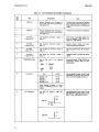
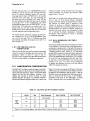
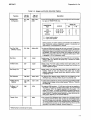
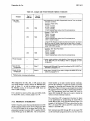
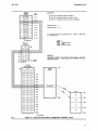
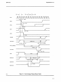
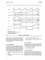
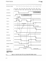
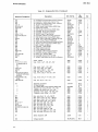
1
rr
iSBC 86/12
SINGLE BOARD COMPUTER
HARDWARE
REFERENCE MANUAL
Manual Order Number: 9800645A
.
Copyright © 197E: Intel Corporation
I
Intel Corporation, 3065 Bowers Av.~nue, Santa Clara, California 95051
L
The infonnation in this manual is subject to change without notice. Intel Corporation makes no warranty of any
kind with regard to this manual, including, but not limited to, the implied warranties of merchantability and
fitness for a particular purpose. Intel Corporation assumes no responsibility for any errors that may appear in this
manual. Intel Corporation makes no commitment to update nor to keep current the infonnation contained
in this manual.
No part of this manual may be copied or reproduced in any fonn or by any means without the prior written consent
of Intel Corporation. The following are trademarks of Intel Corporation and may be used only to describe
Intel products:
ICE· 30
ICE·gO
INSITE
INTEL
INTEU.EC
ii
iSBC
LIBRARY MANAGER
MCS
MEGACHASSIS
MICROMAP
MULTIBUS
PROMPT
UPI
RMX
Printed in U.S,A./B66/0778(TL 7.SK
PREFACE
This manual provides general information, installation, programming information,
principles of operation, and service information for the Intel iSBC 86/12 Single Board
Computer. Additional information is available in the following documents:
8086 Assembly Language Reference Ma~ual, Order No. 9800640
Intel MCS-85 User's Manual, Order No. 98-366
Intel 8255A Programmable Peripheral 1nterface , Application Note AP-15
Intel 8251 Universal Synchronous/Asynchronous Receiver/Transmitter, Application
Note AP-16
• Intel MULTIBUS Interfacing, Application Note AP-28
• Intel 8259 Programmable Interrupt Cm~troller, Application Note AP-31
•
•
•
•
iii
CONTENTS]
CHAPTER 1
GENERAL INFORMATION
PAGE
Introduction .................................... , 1-1
Description ..................................... I-I
System Software Development ..................... 1-3
Equipment Supplied . . . . . . . . . . . . . . . . . . . . . . . . . . . . .. 1-3
Equipment Required .............................. 1-3
Specifications ................................... 1-3
CHAPTER 2
PREPARATION FOR USE
Introduction ..................................... 2-1
Unpacking and Inspection ......................... 2-1
Installation Considerations . . . . . . . . . . . . . . . . . . . . . . . .. 2-1
User-Furnished Components ..................... 2-1
Power Requirement ............................ 2-1
Cooling Requirement ........................... 2-1
Physical Dimensions ............................ 2-1
Component Installation. . . . . . . . . . . . . . . . . . . . . . . . . . .. 2-1
ROM/EPROM Chips ........................... 2-1
Line Drivers and I/O Terminators ................. 2-4
Jumper/Switch Configuration ....................... 2-4
RAM Addresses (Multibus Access) ................ 2-4
Priority Interrupts ... . . . . . . . . . . . . . . . . . . . . . . . . . .. 2-6
Serial I/O Port Configuration. . . . . . . . . . . . . . . . . . . .. 2-9
Parallel I/O Port Configuration ................... 2-9
Multibus Configuration ........................... 2-9
Signal Characteristics .......................... 2-13
Serial Priority Resolution ....................... 2-13
Parallel Priority Resolution ..................... 2-13
Power Fail/Memory Protect Configuration ........... 2-13
Parallel I/O Cabling ............................. 2-23
Serial I/O Cabling ............................... 2-23
Board Installation ............................... 2-23
CHAPTER 3
PROGRAMMING INFORMATION
Introduction . . . . . . . . . . . . . . . . . . . . . . . . . . . . . . . . . . . ..
Failsafe Timer . . . . . . . . . . . . . . . . . . . . . . . . . . . . . . . . . ..
Memory Addressing ..............................
CPU Access ..................................
Multibus Access ................................
I/O Addressing ..................................
System Initialization ..............................
8251A USART Programming ......................
Mode Instruction Fonnat ........................
Sync CharaCters ...............................
Command Instruction Fonnat ....................
Reset ........................................
Addressing ....................................
Initialization ..................................
Operation .....................................
Data Input/Output . . . . . . . . . . . . . . . . . . . . . . . . . . ..
Status Read .................................
3-1
3-1
3-1
3-1
3-2
3-3
3-3
3-4
3-4
3-5
3-5 .
3-5
3-5
3-6
3-7
3-7
3-7
PAGE
8253 PIT Programming ........................... 3-8
Mode Control Word and Count ................... 3-8
Addressing .................................. 3 -12
Initialization ................................. 3 -12
Operation. . . . . . . . . . . . . . . . . . . . . . . . . . . . . . . . . . .. 3-1"3
Counter Read .............................. 3-13
Clock Frequency/Divide Ratio Selection ......... 3-13
Rate Generator/Interval Timer. . . . . . . . . . . . . . . .. 3 -14
Interrupt Timer ............................. 3-14
8255;\ ppl Programming . . . . . . . . . . . . . . . . . . . . . . . .. 3 -14
Control Word Fonnat .......................... 3-15
Addressing .................................. 3-15
Iniitialization ................................. 3-16
Operation. . . . . . . . . . . . . . . . . . . . . . . . . . . . . . . . . . .. 3 -16
Read Operation ............................. 3-16
Write Operation ............................ 3-16
8259A PIC-Programming ......................... 3-17
Interrupt Priority Modes. . . . . . . . . . . . . . . . . . . . . . .. 3 -17
Nested Mode ............................... 3-17
Fully Nested Mode .......................... 3-17
Automatic Rotating Mode .................... 3 -17
Specific Rotating Mode ...................... 3-17
Special Mask Mode ......................... 3-18
Poll Mode ................................. 3-18
Status Read .................................. 3-18
Initialization Command Words .................. 3 -18
Operation Command Words. . . . . . . . . . . . . . . . . . . .. 3 -19
Addressing .................................. 3 -19
Initialization ................................. 3 -19
Operation. . . . . . . . . . . . . . . . . . . . . . . . . . . . . . . . . . .. 3 -19
Hardware Interrupts ............................. 3-25
Non-Maskable Interrupt (NMI) .................. 3-25
Maskable Interrupt (lNTR) ..................... 3-25
Master PIC Byte Identifier .................... 3-25
Slave PIC Byte Identifier ....................• 3-25
CHAPTER 4
PRINCIPLES OF OPERATION
Introduction . . . . . . . . . . . . . . . . . . . . . . . . . . . . . . . . . . . ..
Functional Description ............................
Clock Circuits . . . . . . . . . . . . . . . . . . . . . . . . . . . . . . . ..
Central Processor Unit . . . . . . . . . . . . . . . . . . . . . . . . ..
Interval Timer .................................
Serial I/O .....................................
Parallel I/O ................. . . . . . . . . . . . . . . . . ..
Interrupt Controller .............•...............
ROM/EPROM Configuration .....................
RAM Configuration ............................
Bus Structure .................................
Multibus Interface ............................. ,
4-1
4-1
4-1
4-1
4-1
4-1
4-1
4-2
4-2
4-2
4-2
4-3
iv
I,
CONTENTS (Continued)
PAGE
Circuit Analysis ................................. 4-3
Initialization ................................. 4-4
Clock Circuits ................................. 4-4
Central Processor Unit .......................... 4-4
Basic Timing ................................ 4-4
Bus Timing ................................. 4-4
Address Bus .................................. 4-6
Data Bus ..................................... 4-6
Bus Time Out ............................... " 4-6
Internal Control Signals ......................... 4-8
Dual Port Control Logic ........................... 4-8
Multibus Access Timing ........................ 4-8
CPU Access Timing ............................ 4-8
Multibus Interface. . . . . . . . . . . . . . . . . . . . . . . . . . . . . .. 4-11
I/O Operation .................................. 4-11
On-Board I/O Operation ....................... 4-11
System I/O Operation. . . . . . . . . . . . . . . . . . . . . . . . .. 4-12
ROM/EPROM Operation . . . . . . . . . . . . . . . . . . . . . . . .. 4-12
PAGE
RA\1 Operation ................................
RA\1 Controller . . . . . . . . . . . . . . . . . . . . . . . . . . .
RA\1 Chips ..................................
On-Board Read/Write Operation .................
Bus Read/Write Operation ......................
Byte Operation ............................. "
Interrupt Operation. . . . . . . . . . . . . . . . . . . . . . . . . .. "
NBVlnterrupt ................................
B V Interrupt ............................... "
4-12
4-12
4-13
4-13
4-13
4-13
4-14
4-14
4-14
CHAPTER 5
SERVICE INFORMATION
Introduction .....................................
Replaceable Parts .............................
Service Diagrams ............................
Service and Repair Assistance. . . . . . . . . . . . . . . . . .
5-1
5-1
5-1
5-1
APPENDIX A
TELETYPEWRITER MODIFICATIONS
v
TABLES
I
TABLE
1·1
2·1
2~2
2·3
2·4
2·5
2·6
2·7
2·8
2·9
2·10
2·11
2·12
2·13
2·14
2·15
2·16
2·17
3·}
3·2
3·3
3·4
3·5
TITLE
PAGE
Specifications ........................... 1-4
User-Furnished- and Installed Components .... 2-2
User· Furnished Connector Details ........... 2-3
Line Driver and I/O Terminator Locations . . .. 2-4
Jumper and Switch Selectable Options ....... 2-5
Priority Interrupt Jumper Matrix ............ 2-8
Serial I/O Connector J2 Pin Assignments Vs
Configuration Jumpers ....... : .......... 2-9
Parallel I/O Port Configuration Jumpers ..... 2-10
Multibus Connector PJ. Pin Assignments .... 2-14
Multibus Signal Functions ................ 2-15
iSBC 86/12 DC Characteristics ............ 2-16
iSBC 86/12 AC Characteristics
(Master Mode) ....................... 2-18
iSBC 86/12 AC Characteristics
(Slave Mode) ........ : ............... 2-18
Auxiliary Connector P2 Pin Assignments .... 2-22
Auxiliary Signal (Connector P2)
DC Characteristics ............. '....... 2-22
Parallel I/O Connector 11
Pin Assignments ...................... 2-23
Parallel I/O Signal (Connector 11)
DC Characteristics .................... 2-24
Connector J2 Vs RS232C Pin
Correspondence ....................... 2-24
On -Board Memory Addresses
(CPU Access) ......................... 3-2
I/O Address Assignments .................. 3-3
Typical USART Mode or Command
Instruction Subroutine .................. 3 -7
Typical USART Data, Character Read
Subroutine ............................ 3-8
Typical USART Data Character Write
Subroutine ............................ 3-8
TABLE
3-6
3-7
3-8
3-9
3-10
3-11
3-12
3-13
3-14
3-15
3-16
3-17
3-18
3-19
3-20
3-21
3-22
3-23
3·24
3-25
5-1
5-2
TITLE
PAGE
Typical US ART Status Read Subroutine ..... 3-9
PIT Counter Operation Vs Gate Inputs ...... 3·12
Typical PIT Control Word Subroutine ...... 3-12
Typical PIT Count Value Load
Subroutine ........................... 3·12
Typical PIT Counter Read Subroutine ...... 3-13
PIT Count Value Vs Rate Multiplier for
Each Baud Rate ...................... 3-14
PIT Rate Generator Frequencies and
Timer Intervals . . . . . . . . . . . . . . .. . . . . . .. 3 -15
PIT Time Intervals Vs Timer Counts ....... 3-15
Typical PPI Initialization Subroutine. . . . . . .. 3-16
Typical PPI Port Read Subroutine .......... 3-16
Typical PPI Port Write Subroutine ......... 3-16
Typical PIC Initialization Subroutine
(NBV Mode) ......................... 3-21
Typical Master PIC Initialization Subroutine
(BV Mode) .......................... 3-21
Typical Slave PIC Initialization Subroutine
(BV Mode) .......................... 3-22
PIC Operation Procedures ................ 3-22
Typical PIC Interrupt Request
Register Read Subroutine ............... 3-24
Typical PIC In-Service Register
Read Subroutine ...................... 3-24
Typical PIC Set Mask Register Subroutine ... 3-24
Typical PIC Mask Register Read
Subroutine ........................... 3-24
Typical PIC End-of-Interrupt Command
Subroutine ........................... 3-25
Replaceable Parts ........................ 5-1
List of Manufacturers' Codes .............. 5·3
vi
Ij'
ILLUSTRATIONS
FIGURE
I-I
2-1
2-2
2-3
2-4
2-5
2-6
3-1
3-2
3-3
3-4
3-5
3-6
3-7
3-8
3-9
3-10
TITLE
PAGE
iSBC 86/12 Single Board Computer ......... I-I
Dual Port RAM Address Configuration
(Multibus Access) ...................... 2-7
Simplified Master/Slave PIC
Interconnect Example ................... 2-8
Bus Exchange Timing (Master Mode) ...... 2-19
Bus Exchange Timing (Slave Mode) ........ 2-20
Serial Priority Resolution Scheme .......... 2-21
Parallel Priority Resolution Scheme ........ 2-21
Dual Port RAM Addressing
(Multibus Access) ...................... 3-2
USART Synchronous Mode Instruction
Word Format .......................... 3-4
USART Synchronous Mode Transmission
Format ............................... 3-4
US ART Asynchronous Mode Instruction
Word Format .......................... 3-5
USART Asynchronous Mode Transmission
Format ............................... 3-5
USART Command Instruction
Word Format ............................ 3-6
Typical USART Initialization and
I/O Data Sequence ..................... 3-6
USART Status Read Format ............... 3-9
PIT Mode Control Word Format ........... 3-10
PIT Programming Sequence Examples ...... 3-11
FIGURE
3-11
3-12
3-13
3-14
3-15
4-1
4-2
4-3
4-4
4-5
4-6
4-7
4-8
5-1
5-2
5-3
5-4
TITLE
PAGE
PIT Counter Register Latch Control
Word Format ..................... .
3-13
PPI Control Word Format ............... . 3-15
PPI Port C Bit Set/Reset Control
Word Format. ................... .
3-17
PIC Initialization Command
Word Formats ................... .
3-18
PIC Operation Control Word Formats ... .
3-20
iSBC 86/12 Input/Output and Interrupt
4-15
Simplified Logic Diagram. . . . . . . . . .
iSBC 86/12 ROM/EPROM and Dual Port RAM
Simplified Logic Diagram " ............ 4-17
Internal Bus Structure ................... " 4-3
CPU Read Timing ........... , ........... 4-5
CPU Write Timing ....................... 4-6
CPU Interrupt Acknowledge
Cycle Timing ......................... 4-7
Dual Port Control Multibus Access
Timing With CPU Lockout .. . . . . . . . . . . .. 4-9
Dual Port Control CPU Access Timing
With Multibus Lockout ................ 4-10
iSBC 86/12 PaJ1s Location Diagram ......... 5-6
iSBC 86/12 Schematic Diagram ............ 5-7
iSBC 604 Schematic Diagram ............. 5-29
iSBC 614 Schematic Diagram ............. 5-31
vii/viii
CHAPTER 1
GENERAL INFORMATION
1-1. INTRODUCTION
The iSBC 86/12 Single Board Computer, which is a
member of Intel's complete line of iSBC 80/86 computer
products, is a complete computer system on a single
printed-circuit assembly. The iSBC 86/12 includes a
16-bit central processing unit (CPU), 32K bytes of
dynamic RAM, a serial communications interface, three
programmable parallel I/O ports, programmable timers,
priority interrupt control, Multibus control logic, and bus
expansion drivers for interface with other Multibuscompatible expansion boards. Also included is dual port
control logic to allow the iSBC 86/12 to act as a slave
RAM device to other Multibus masters in the system.
Provision is made for user installation of up to 16K bytes
of read only memory.
addition, the CPU contains two 16-bit pointer registers
and two 16-bit index registers. Four 16-bit segment registers allow extended addressing to a full megabyte of
memory. The CPU instruction set supports a wide range
of addressing modes and data transfer operations, signed
and unsigned 8-bit and 16-bit arithmetic including
hardware mUltiply and divide, and logical and string operations. The CPU architecture features dynamic code relocation, reentrant code, and instruction lookahead.
The iSBC 86/12 has an internal bus for all on-board
memory and I/O operations and accesses the system bus
(Multibus) for all external memory and I/O operations.
Hence, local (on-board) operations do not involve the
Multibus, making the Multibus available for true parallel
processing when several bus masters (e. g., DMA devices
and other single board computers) are used in a multimaster scheme.
1-2. DESCRIPTION
The iSBC 86/12 Single Board Computer (figure 1-1) is
controlled by an Intel 8086 16-Bit Microprocessor (CPU) .
The 8086 CPU includes four 16-bit general purpose registers that may also be addressed as eight 8-bit registers. In
Dual port control logic is included to interface the
dynamic RAM with the Multibus so that the iSBC 86/12
can function as a slave RAM device when not in control of
the Multibus. The CPU has priority when accessing onboard RAM. After the CPU completes its read or write
(MULTIBUS)
645-1
(AUXIUARy)
f4'igure 1-1. iSBC 86/12 Single Board Computer
1-1
iSBC 86/12
General Information
operation, the controlling bus master is allowed to access
RAM and complete its operation. Where both the CPU
and the controlling bus master have the need to write or
read several bytes or words to or from on-board RAM,
their operations ary interleaved. For CPU access, the
on-board RAM addresses are assigned from the bottom up
of the I-megabyte address space; i.e., 0OOOO-07FFFH·
The slave RAM address decode logic includes jumpers
and switchers to allow partitioning the on-based RAM
into any 128K segment of the 1-megabyte system address
space.
The slave RAM can be configured to allow either 8K, 16K
24K, or 32K access by another bus master. Thus, the
RAM can be configured to allow other bus masters to
access a segment of the on-board RAM and still reserve
another segment strictly for on-board use. The addressing
scheme accommodates both 16-bit and 20-bitaddressing.
Four IC sockets are included to accommodate up to 16K
bytes of user-installed read only memory. Configuration
jumpers allow read only memory to be installed in 2K,
4K, or 8K increments.
The iSBC 86/12 includes 24 programmable parallel I/O
lines implemented by means of an Intel 8255A Programmable Peripheral Interface (PPI). The system
software is used to configure the I/O lines in any combination of unidirectional input/output and bidirectional ports.
The I/O interface may be customized to meet specific
peripheral requirements and, in order to take full advantage of the large number of possible I/O configurations, IC
sockets are provided for interchangeable I/O line drivers
and terminators. Hence, the flexibility of the parallel I/O
interface is further enhanced by the capability of selecting
the appropriate combination of optional line drivers and
terminators'to provide the required sink current, polarity,
and drive/termination characteristics for each application.
The 24-programmable I/O ,lines and signal ground lines
are brought out to a 50-pin edge connector (11) that mates
with flat, woven, or round cable.
..
The RS232C compatible serial I/O port is controlled arid
interfaced by an Intel 8251A US ART (Universal
Syncronous/Asynchrortous ReceiverlTransmitter) chip.
The USART is individually programmable for operation
in most synchronous or asynchronous serial data transmission formats (including· iBM Bi-Sync).
In the synchronous mode the following are programma- .
ble:
a.
Character length,
b.
Sync character (or chlU1lcters), and
c.
Parity.
1-2
In the asynchronous mode the following are programmable:
a.
Character length,
b.
Baud rate factor (clock divide ratios of 1, 16, or 64),
c.
d.
Stop bits, and
Parity.
In both the synchronous and asychronous modes, the
serial I/O port features half- or full-duplex, double buffered transmit and receive capability. In addition, USART
error detection circuits can check for parity, overrun, and
framing errors. The USART transmit and receive clock
rates are supplied by a programmable baud rate/time
generator. These clocks may optionally be supplied from
an external source. The RS232C command lines, serial
data lines, and signal ground lines are brought out to a
50-pin edge connector (12) that mates with flat or round
cable.
Three independent, fully programmable 16-bit interval
timer/event counters are provided by an Intel 8253 Programmable Interval Timer (PIT). Each counter is capable
of operating in either BCD or binary modes; two of these
counters are available to the systems designer to generate
accurate time intervals under software control. Routing
for the outputs and gate /trigger inputs of two of these
counters may be independently routed to the 8259A Programmable Interrupt Controller (PIC). The gate/trigger inputs of the two counters may be routed to I/O terminators
associated with the 8255A PPI or as input connections
from the 8255A PPI. The third counter is used as a
programmable baud rate generator for the serial I/O port.
In utilizing the iSBC 86/12, the systems designer simply
configures, via software, each counter independently to
meet system requirements. Whenever a given time delay
or count is needed, software commands to the 8253 PIT
select the desired function. The contents of each counter
may be read at any time during system operation with
simple operations for event counting applications, and
special commands are included ~ that the contents of
each counter·can be read "on the fly".
The iSBC 86/ 12 provides vectoring for bus vectored (B V)
~ruid non-bus vectored (NBY) interrupts. An on-board
In.tel 8259A Programmable Interrupt Controller (PIC)
handles up to eight NBV interrupts. By using external
PIC's slaved. to the on-board PIC (master), the interrupt
structure can be expanded to handle and resolve the priorityof upto 64 BV sources.
The PIC, which can be programmed to respond to edgesensitive or level-sensitive inputs, treats each true input
signal condition as an interrupt request. After resolving
the interrupt priority, the PIC issues a single interrupt
request to the ·CPU. Interrupt priorities are independently
programmable under software control. The programmable interrupt priority modes are:
General Information
iSBC 86/12
a.
Fully Nested Priority. Each interrupt request has a
fixed priority: input 0 is highest, input 7 is lowest.
b.
Auto-Rotating Priority. Each interrupt request has
equal priority. Each level, after receiving service,
becomes the lowest priority level until the next interrupt occurs.
c.
Specific priority. Software assigns lowest priority.
Priority of all other levels is in numerical sequence
based on lowest priority.
The CPU includes a non-maskable interrupt (NMI) and a
maskable interrupt (lNTR). The NMI interrupt is intended
to be used for catastrophic events such as power outages
that require immediate action of the CPU. The INTR
interrrupt is driven by the 8259A PIC which, on demand,
provides an 8-bit identifier of the interrupting source. The
C~U multiplies the 8-bit identifier by four to derive a
pomter to the service routine for the interrupting device.
Interrupt requests may originate from 18 sources without
the necessity of external hardware. Two jumperselectable interrupt requests can be automatically generated by the Programmable Peripheral Interface (PPI)
when a byte of information is ready to be transferred to the
~086 CPU (i.e., input buffer is full) or a byte of informatIOn has been transferred to a peripheral device (i.e.,
output buffer is empty). Two jumper-selectable interrupt
requests can be automatically generated by the US ART
when a character is ready to be transferred to the 8086
CPU (i.e., receive channel buffer is full) or when a
character is ready to be transmitted (i.e., transmit channel
data buffer is empty.) A jumper-selectable interrupt
request can be generated by two of the programmable
counters and eight additional interrupt request lines are
ava.ilable to the user for direct interfaces to user-designated
penpheral devices via the Multibus. One interrupt request
line may be jumper routed directly from a peripheral via
th~ ~arallel VO driverlterminator section and one power
fall mterrupt may be input via auxiliary connector P2.
Th~ iSBC 86/12 includes the resources for supporting a
~anety of OEM system requirements. For those applica-
tIOns requiring additional processing capacity and the
benefits of multiprocessing (Le., several CPU's and/or
controllers logically sharing systems tasks with communication over the Multibus), the iSBC 86/12 provides
full bus arbitration control logic . This control logic allows
up to three bus masters (e.g., combination of iSBC 86/12
DMA controller, diskette controller, etc.) to share the
Multibus in serial (daisy-chain) fashion or up to 16 bus
masters to share the Multibus using an external parallel
priority resolving network.
lers to share resources on the same bus,. and transfers via
~he bus proceed asynchronously. Thus, the transfer speed
IS dependent on transmitting and receiving devices only.
This design prevents slower master modules from being
handicapped in their attempts to gain control of the bus,
but does not restrict the speed at which faster modules can
transfer data via the same bus. The most obvious applications for the master-slave capabilities of the bus are multiprocessor configurations, high-speed direct memory
access (DMA) operations, and high-speed peripheral
control, but are by no means limited to these three.
1-3. SYSTEM SOFTWARE
DEVELOPMENT
The development cycle of iSBC 86/12 based products
may be significantly reduced using an Intel Intellec Microcomputer Development System. The resident text editor
and system monitor greatly simplify the design, develop~ent, and deb~g of iSBC system software. An optional
dIskette operatmg system provides a relocating loader and
linkage editor, and a library manager.
Intel's high level programming language, PUM86, is also
available as a resident Intellec Microcomputer Development System option. PUM 86 provides the capability to
program in a natural, algorithmic language and eliminates
the need to manage register usage or allocate memory.
PUM 86 programs can be written in a much shorter time
than assembly language programs for a given application.
1-4. EQUIPMENT SUPPLIED
The following are supplied with the iSBC 86/12 Single
Board Computer:
a.
Schematic diagram, dwg no. 2002259
b.
Assembly drawing, dwg no. 1001801
1-5. EQUIPMENT REQUIRED
Because the iSBC 86/12 is designed to satisfy a variety of
applications, the user must purchase and install only those
components required to satisfy his particular needs. A list
of components required to configure all the intended applications of the iSBC86/12 is provided in table 2-1.
T~e
Multibus arbitration logic operates synchronously
WIth the bus clock, which is derived either from the iSBC
86/12 or can be optionally generated by some other bus
master. Data, however, is transferred via a handshake
between the controlling master and the addressed slave
module. This arrangement allows different speed control-
1-6. SPECIFICATIONS
Specifications of the iSBC 86/12 Single Board Computer
are listed in table 1-1.
1-3
iSBC 86/12
General Information
Table 1-1. Specifications
WORD SIZE
Instruction:
Data
CYCLE TIME:
8, 16, 24, or 32 bits.
8/16 bits.
800 nanosecond for fastest executable instruction (assumes instruction is in the queue).
1.2 microseconds for fastest executable instruction (assumes instruction is not in the
queue).
MEMORY CAPACITY
On-Board ROM/EPROM:
Up to 16K bytes; user installed in 1K, 2K, or 4K byte increments.
On-Board Dynamic RAM:
32K bytes. Integrity maintained during power failure with user-furnished batteries.
Off-Board Expansion:
Up to 1 megabyte of user-specified combination of RAM, ROM, and EPROM.
MEMORY ADDRESSING
On-Board ROM/EPROM:
On-Board RAM:
(CPU Access)
On-Board RAM:
(Multi bus Access)
SERIAL COMMUNICATIONS
Synchronous:
Asynchronous:
FFOOO-FFFFFH (using 2758 EPROM's),
FEOOO-FFFFFH (using 2316E ROM's or 2716 EPROM's), and
FCOOO-FFfFFH (using 2332 ROM's).
00000-07FFFH .
Jumpers and switches allow board to act as slave RAM device for access by another
bus master. Addresses may be set within any 8K boundary of any 128K segment of the
1-megabyte system address space. Access is selectable for 8K, 16K, 24K, or32K bytes.
5-, 6-, 7-, or 8-bit characters.
Intemal; 1 or 2 sync characters.
Automatic sync insertion.
5-, 6-, 7-, or 8-bit characters.
Break character generation.
1, 1Y2, or 2 stop bits.
False start bit detection.
Sample Baud Rate:
Baud Rate (Hz)2
Frequency'
(kHz, Software Selectable)
153.6
76.8
38.4
19.2
9.6
4.8
2.4
1.76
Synchronous
38400
19200
9600
4800
2400
1760
Asynchronous
+16
+64
9600
4800
2400
1200
600
300
150
110
2400
1200
600
300
150
75
-
-
Notes: 1. Frequency selected by I/O writes of appropriate 16-bit freq uency factor to
Baud Rate Register.
2. Baud rates shown here are only a sample subset of possible softwareprogrammable rates available. Any frequency from 18.75 Hz to 613.5 kHz
may be generated utilizing on-board crystal oscillator and 16-bit Programmable Interval T'imer (used here as frequency divider).
1-4
General Information
JSBC 86/12
Table 1-1. Specifications (Continued)
INTERVAl TIMER AND BAUD RATE
GENERATOR
Input Frequency (selectable):
2.46 MHz ±0.1% (0.41 jLsec period nominal),
1.23 MHz ±0.1% (0.82 jLsec period nominal), and
153.6 kHz ±0.1% (6.5 jLsec period nominal).
Output Frequencies:
Single Timer
Function
Dual Timers
(Two Timers Cascaded)
Min.
Max.
Min.
Max.
Real-Time
Interrupt
Interval
1.63 jLsec
427.1 msec
3.26 jLsec
466.5
minutes
Rate
Generator
(Frequency)
2.342 Hz
613.5 kHz
0.000036 Hz
306.8 kHz
SYSTEM CLOCK (8086 CPU):
5.0 MHz ±0.1%.
I/O ADDRESSING:
All communication to Parallel I/O and Serial I/O Ports, Timer, and InterruptControlier
is via read and write commands from on-board 8086 CPU. Refer to table 3-2.
INTERFACE COMPATIBILITY
Serial I/O:
EIA Standard RS232C signals
Clear to Send
Data Set Ready
Data Terminal Ready
Request to Send
Receive Clock
provided and supported:
Receive Data
Secondary Receive Data*
Secondary CTS*
Transmit Clock*
Transmit Data
*Can support only one.
Parallel I/O:
24 programmable lines (8 lines per port); one port indudes bidirectional bus driver.
IC sockets included for user installation of line drivers and/or I/O terminators as
required for interface ports. Refer to table 2-1.
INTERRUPTS:
8086 CPU includes non-maskable interrupt (NMI) and maskable interrupt (INTR).
NMI interrupt is provided for catastrophic event such as power failure; NMI vector
address is 00008. INTR interrupt is driven by on-board 8259A PIC, which provides
8-bit identifier of interrupting device to CPU. CPU multiplies identifier by four to derive
vector address. Jumpers select interrupts from 18 sources without necessity of
external hardware. PIC may be programmed to accommodate edge-sensitive or
level-sensitive inputs.
COMPATIBLE CONNECTORS/CABLES:
Refer to table 2-2 for compatible connector details. Refer to paragraphs 2-21 and
2-22 for recommended types and lengths of I/O cables.
ENVIRONMENTAL REQUIREMENTS
Operating Temperature:
Relative Humidity:
PHYSICAl CHARACTERISTICS
Width:
Height:
Thickness:
Weight:
To 90% without condensation.
30.48 cm (12.00 inches).
17.15 em (6.75 inches).
1.78 cm (0.7 inch).
539 gm (19 ounces).
1-5
iSBC 86/12
General Information
Table 1-1. Specifications (Continued)
POWER REQUIREMENTS:
CONFIGURATION
Without EPROM'
VCC
=
+5V±5%
VOO
=
+12V±5%
VBB
=
-5V±5%
-
VAA
=
-12V±5%
40 rnA
5.2A
350 rnA
390 rnA
40 rnA
With iSBC 53()4
5.2A
450 rnA
-
140 rnA
With 4K EPROMs
(Using 2758)
5.5A
450 rnA
-
140 rnA
With 8K ROMS
(Using 2316E)
6.1A
450 rnA
-
140 rnA
With 8K EPROMs
(Using 2716)
5.5A
450 rnA
-
140 rnA
With 16K ROMS
(Using 2332)
5.4A
450 rnA
-
140 rnA
RAM Only3
Notes: 1. Does not include power for optional ROM/EPROM,
1.0 rnA
-
110 drivers, and 110 terminators.
110 terminators.
2. Does not include power required for optional ROM/EPROM, 1/0 drivers, and
3. RAM chips powered via auxiliary power bus.
4. Does not include power for optional ROM/EPROM,
via serial port connector.
110 drivers, and 110 terminators. Power for iSBC 530 is supplied
5. Includes power required for four ROM/EPROM chips, and
inputs low.
1-6
110 terminators installed for16 110 lines; all terminator
CHAPTER 2
PREPARATION FOR USE
2-1. INTRODUCTION
2-5. POWER REQUIREMENT
This chapter provides instructions for the iSBC 86/12
Single Board Computer in the user-defined environment.
It is advisable that the contents of Chapters 1 and 3 be
fully understood before beginning the configuration and
installation procedures provided in this chapter.
The iSBC 86/12 requires +5V, -5V, + 12V, and -12V
power. The -5V power, which is required only for the
dual port RAM, can be supplied by the system -5V
supply, an auxiliary battery, or by the on-board -5V
regulator. (The -5V regulator operates from the system
-12V supply.)
2-2. UNPACKING AND INSPECTION
2-6. COOLING REQUIREMENT
Inspect the shipping carton immediately upon receipt for
evidence of mishandling during transit. If the shipping
carton is severely damaged or waterstained, request that
the carrier's agent be present when the carton is opened.
If the carrier's agent is not present when the carton is
opened and the contents of the carton are damaged,
keep the carton and packing material for the agent's
inspection.
The iSBC 86/12 dissipates 451 gram-calories/minute
(1.83 Btu/minute) and adequate circulation of air must be
provided to prevent a temperature rise above 55°C
(131°F). The System 80 enclosures and the Intellec System include fans to provide adequate intake and exhaust of
ventilating air.
2-7. PHYSICAL DIMENSIONS
For repairs to a product damaged in shipment, contact
the Intel Technical Support Center (see paragraph 5-3)
to obtain a Return Authorization Number and further
instructions. A purchase order will be required to complete the repair. A copy of the purchase order should be
submitted to the carrier with your claim.
It is suggested that salvageable shipping cartons and packing material be saved for future use in the event the product must be reshipped.
2-8. COMPONENT INSTALLATION
2-3. INSTALLATION CONSIDERATIONS
The iSBC 86/12 is designed for use in one ofthe following configurations:
(single~board)
a.
Standalone
b.
Bus master in a single bus master system.
c.
Bus master in a multiple bus master system.
system.
Important criteria for installing and interfacing the
iSBC 86/12 in these configurations are presented in
following paragraphs.
2-4. USER-FURNISHED COMPONENTS
The user-furnished components required to configure the
iSBC86/12 for a particular application are listed in table
2-1. Various types and vendors of the connectors specified in table 2-1 are listed in table 2-2.
Physical dimensions of the iSBC 86/12 are as follows:
a.
Width:
30.48 cm (12.00 inches).
b.
Height:
17.15 cm (6.75 inches).
c.
Thickness:
1.78 cm (0.70 inch).
Instructions for installing optional ROM/EPROM and
parallel I/O port line drivers and/or line terminators are
given in following paragraphs. When installing these chip
components, be sure to orient pin 1 of the chip adjacent
to the white dot located near pin 1 of the associated
IC socket. The grid zone location on figure 5-1 (pltrts
location diagram) is specified for each component chip to
be installed.
2-9. ROM/EPROM CHIPS
IC sockets A28, A29, A46, and A47 (figure 5-1 zone C3)
accommodate 24-pin ROM/EPROM chips. Because the
CPU jumps to location FFFFO on a power up or reset, the
ROM/EPROM address space resides in the topmost portion of the I-megabyte address space and must be loaded
from the top down. IC sockets A29 and A47 accommodate the top of the ROM/EPROM address space and
must always be loaded; IC sockets A28 and A46 accommodate the ROM/EPROM space directly below that installed in A29 and A47.
2-1
Preparation for Use
iSBC 86112
Table 2-1. User-Furnished and Installed Components
Item
No.
Item
Description
Use
1
iSBC 604
Modular Backplane and Cardcage. Includes four slots with bus terminators.
(See figure 5-3.)
Provides power input pins and Multibus
signal interface between iSBC 86/12 and
three additional boards in a multiple board
system.
-
2
iSBC 614
Modular Backplane and Cardcage. Includes four slots without bus terminators.
(See figure 5-4.)
Provides four-slot extension of iSBC 604.
3
Connector
(mates with P1)
See Multibus Connector details in
table 2-2.
Power inputs and Multibus signal interface. Not required if iSBC 86/12 is installed in an iSBC 6041614.
4
Connector
(mates with P2)
See Auxiliary Connector details in
table 2-2.
Auxiliary backup battery and
ciated memory protect functions.
5
Connector
(mates with J1)
See Parallel I/O Connector details in
table 2-2.
Interfaces parallel I/O port with Intel8255A
PPI.
6
Connector
(mates with J2)
See Serial I/O connector details in
table 2-2.
Interfaces serial I/O port with Intel 8251A
USART.
7
ROM/EPROM Chips
Two or four each of the following
types:
Ultraviolet Erasable PROM (EPROM) for
development. Masked ROM for dedicated program.
ROM
or
EPROM
-
2758
2716
2316E
2332
8
Une Drivers
asso-
-
Type
Current
SN7403I,OC
SN7400 I
SN7408 NI
SN7409 NI, OC
16mA
16mA
16mA
16mA
Interface parallel I/O ports CA and CC with
Intel 8255A PPI. Requres two line driver
IC's for each 8-bit parallel output port.
Types selected as typical; I = inverting, NI = noninverting, and OC = open
collector.
9
Une Terminators
Intel iSBC 901 Divider or iSBC 902
Pull-Up:
+5V
220
iSBC 901
A
.&
r:v
iSBC 902
0
2-2
330
0
Interface parallel"VO ports CA and CC with
Intel8255A PPI. Requires two 901's ortwo
902'sfor each 8-bit parallel input port.
iSBC 86/12
Preparation for Use
Table 2-2. User-Furnished Connector Details
Function
No. Of
Pairs/
Pins
Centers
(inches)
Connector
Type
Vendor
Vendor Part No.
Intel
Part No.
3415-0000 WITH EARS
3415-0001 W/O EARS
88083-1
609-5015
S06750 SERIES
iSBC 956
Cable
Set
2-583485-6
3VH25/1JV5
H312125
N/A
Parallel
I/O
Connector
25/50
0.1
Flat Crimp
3M
3M
AMP
ANSLEY
SAE
Parallel
I/O
Connector
25/50
0.1
Soldered
AMP
VIKING
TI
Wirewrap'
TI
VIKING
COO
ITICANNON
H311125
3VH25/1JN05
VPB01 B25000A1
EC4A050A1A
N/A
3M
AMP
ANSLEY
SAE
3462-0001
88106-1
609-2615
S06726 SERIES
iSBC 955
Cable
Set
Parallel
I/O
Connector
. 24/50
0.1
Serial
110
13/26
0.1
Flat Crimp
13/26
0.1
Soldered
13/26
0.1
Wi rew rap'
TI
Connector
Serial
110
Connector
TI
AMP
H312113
1-583485-5
N/A
H311113
N/A
VPB01 E43000A1
MP-0156-43-BW-4
AE443WP1 LESS EARS
2VH43/1AV5
N/A
Serial
110
Connector
Multibus
Connector
43/86
0.156
Soldered'
COC3
MICRO PLASTICS
ARCO
VIKING
Multibus
Connector
43/86
0.156
Wirewrap1.2
COO
COC3
VIKING
VFB01 E43000A 1 or
VPB01E43AooA1
2VH43/1AV5
Auxiliary
Connector
30/60
0.1
Soldered'
TI
VIKING
H312130
3VH30/1JN5
N/A
Auxiliary
Connector
30/60
0.1
Wirewrap1.2
COO
TI
VPB01 B30AOOA2
H311130
N/A
:,
MOS 985
NOTES:
1.
Connector heights are not guaranteed to conform to OEM packaging equipment.
2.
Wirewrap pin lengths are not guaranteed to conform to OEM packaging equipment.
3.
COC VPB01 .... VPB02 .... VPB04 .... etc. are identical connectors with different electroplating thicknesses or
metal surfaces.
2-3
iSBC 86/12
Preparation for Use
The low-order byte (bits 0-7) of ROM/EPROM must be
installed in sockets A29 and A28; the high-order byte
(bits 8-15) must be installed in sockets A47 and A46.
Assuming that 2K bytes of EPROM are to be installed
using two Intel 2758 chips, the chip containing the
low-order byte must be installed in IC socket A29 and
the chip containing the high-order byte must be installed
in IC socket A47. In this configuration, the usable
ROM/EPROM address space is FF800-FFFFF. Two additional Intel 2758 chips may be installed later in IC
sockets A28 and A46 and occupy the address space
FFOOO-FF7FF. (Even addresses read the low-order bytes
and odd addresses read the high-order bytes.)
The default (factory connected) jumpers and switch S 1
are configured for 2K by 8-bit ROM/EPROM chips
(e.g., two or four Intel 2716's). If different type chips
are installed, reconfigure the jumpers and switch S 1 as
listed in table 2-4.
2-10. LINE DRIVERS AND I/O
TERMINATORS
Table 2-3 lists the I/O ports and the location of associated
14-pin IC sockets for instaHing either line drivers or I/O
tenninators. (Refer to table 2-1 items 8 and 9.)
Port C8 is factory equipped with Intel 8226 Bidirectional
Bus Drivers and requires no additional components.
references to figure 5-2 may be either four or five alphanumeric characters. For exampfe, grid reference 3ZB7
signifies sheet 3 Zone B7.
Study table 2-4 carefully while making reference to figures 5-1 and 5-2. If the default (factory configured)
jumpers and switch settings are appropriate for a particular function, no further action is required for that
function. If, however, a different configuration is required, reconfigure the switch settings and/or remove the
default jumper(s) and install an optional jumper(s) as
specified. For most options, the infonnation in table
2-4 is sufficient for proper configuration. Additional
information, where necessary for clarity, is described
in subsequent paragraphs.
2-12. RAM ADDRESSES (MULTIBUS
ACCESS)
The dual port RAM can be shared with other bus masters
via the Multibus. One jumper wire connected between a
selected pair of jumper posts (113 through 128) places the
dual port RAM in one of eight 128K byte segments of the
I-megabyte address space. Switch S 1 is a dual-inline
package (DIP) composed of eight individual single-pole,
single-throw switches. (Two of these individual switches
are used for ROM/EPROM configuration.) Two switches
(6-11 and 5-12) are configured to allow 8K, 16K, 24K,
or 32K bytes of dual port RAM to be accessed. Four
switches (1-16, 2-15, 3-14, and 4-13) are configured
to displace the addresses from the top of the selected
128K byte segment of memory.
2-11. JUMPER/SWITCH CONFIGURATION
The iSBC :86/12 includes a variety of jumper- and switchselectable options to allow the user to configure the board
for his particular application. Table 2-4 summarizes these
options and lists the grid reference locations of the
jumpers and switches as shown in figure 5-1 (parts
location diagram) and figure 5-2 (schematic diagram).
Because the schematic dIagram consists of 11 sheets, gria
Figure 2-1 provides an example of 8K bytes of dual port
RAM being made accessible from the Multibus and how
the addresses are established. Note in figure 2-1 that the
Multibus accesses the dual port RAM from the top down.
Thus, as shown for 8K byte access via the Multibus,
the bottom 24Kbytes of the iSBC 86/12 on-board
RAM is reserved strictly for on-board CPU access.
Table 2-3. Line Driver and I/O Terminator Locations
8255A
PPI
Interface
Bits
DriverlTermlnator
Fig. 5-1 Grid Ref.
C8
0-7
None Required
-
0-3
A12
A13
lO4
lO4
9ZA3
9ZA3
A11
A10
lO5
lO5
9lC3
CA
CC
4-7
0-3
4-7
*Figure 5-2 is the schematic diagram. Grid reference 9ZA3, for example, denotes sheet 9
2-4
Fig. 5-2* Grid Ref.
1/0 Port
-
9lB3
lone A3.
i8BC 86/12
Preparation for Use
Table 2-4. Jumper and Switch Selectable Options
Function
Fig. 5-1
Grid Ref.
Fig. 5-2
Grid Ref.
Description
ROM/EPROM
Configuration
ZC3, ZB6,
ZD7
6ZB3,6ZC7,
2ZB6
Jumpers 94 through 99 and switch S1 may be configured to accommodate
four types of ROM/EPROM chips:
ROM/EPROM
Type
2758
2316E/2716
2332
Reserved
C
= closed
Switch S1
-- --
Jumpers
94-95, 97 -98
*94-96, *97-98
94-96, 97-99
-
8-9
7-10
C
*C
0
0
C
*0
C
0
switch position.
o = open switch position.
Default jumpers and switch settings accommodate Intel 2316E/2716
chips. Disconnect existing configuration jumpers (if necessary) and
reset switch S1 if reconfiguration is required.
Dual Port RAM
(Multibus Access)
ZB7, ZB6
3ZB6,3ZB7
The dual port RAM permits access by the local (on-board) CPU and any
system bus master via the Multibus. For local CPU access, the dual port
RAM address space is fixed beginning at location 00000. For access via
the Multibus, one jumper and one switch can configure the dual port
RAM on any 8K boundary within the 1-megabyte address space. Refer
to paragraph 2-12 for configuration details.
Bus Clock
ZB7
10ZA2
Default jumper *105-106 routes Bus Clock signal BCLKI to the Multibus.
(Refer to table 2-9.) Remove this jumper only if another bus master
supplies this signal.
Constant Clock
ZB7
10ZA2
Default jumper *103-104 routes Constant Clock signal CCLKI to the
Multibus. (Refer to table 2-9.) Remove this jumper only if another bus
master supplies this signal.
Bus Priority Out
ZB7
3ZD2
Default jumper *151-152 routes Bus Priority Out signal BPRO/ to the
Multibus. (Refer to table 2-9.) Remove this jumper only in those
systems employing a parallel priority bus resolution scheme. (Refer
to paragraph 2-19.)
Bus Arbitration
ZBB, Zf)7
3ZD2,3ZC3
The Common . Bus Request signal (CBRO)
the Multibus and the
ANYROST input to the Bus Arbiter chip are not presently used.
Auxiliary Backup
Batteries
ZD3, ZBB,
ZB5
1ZC7,1ZCB
If auxiliary backup batteries are used to sustain the dual port RAM conter1'ts
du~ng ac power outages, remove default jumpers *W4(A-B), *W5(A-B),
and *W6(A-B).
..
On-Board -5V
Regulator
ZB6
1ZCB
The dual port RAM requires a -5V AUX input, which can be supplied by
the system -5V supply, an auxiliary backup battery, or by the,on-board
-5V regulator. (The -5V regulator operates from the system -12V
supply.) If a system -5V supply is available and auxiliary backup batteries are not used, disconnect default jumper *W5(A-B) and connect
jumper W5(B-C). If auxiliary backup batteries are used, disconnect default jumper *W5(A-B); do not connect W5(B-C).
Failsafe Timer
ZD7
2ZB6
If the on-board CPU addresses either a system or an on-board memory
or I/O device and that device does not return an acknowledge Signal,
the CPU will hang up in a wait state. A failsafe timer is triggered during
T1 of every machine cycle and, if not retriggered within 6.2 milliseconds,
the resultant time-out pulse can be used to allow the CPU to exit the
wait state. If this feature is desired, connect jumper 5-6.
trom
*Default jumper connected at the factory.
2-5
Preparation for Use
iSBC 86/12
Table 2-4. Jumper and Switch Selectable Options (Continued)
Function
Fig. 5-1
Grid Ref.
Fig. 5-2
Grid Ref.
Timer Input
Frequency
Description
Input frequencies to the 8253 Programmable Interval Timer are jumper
selectable as follows:
Counter 0 (TMRO INTR)
ZD3
7ZB5
57-58:
*57-56:
57 -53:
57-62:
153.6 kHz.
1.23 MHz.
2.46 MHz.
Extemal Clock to/from Port CC terminator/driver.
Counter 1 (TMR1 INTR)
ZD3
7ZA5
*59-60:
59-56:
*59-53:
59-62:
59-61:
153.6 kHz.
1.23 MHz.
2.46 MHz.
External Clock to/from Port CC terminator/driver.
Counter 0 output.
Jumper 59-61 effectively connects Counter 0 and Counter 1 in series in
which.the output of Counter 0 serves as the input clock to Counter 1.
This permits programming the clock rates to Counter 1 and thus provide
longer TMR1 INTR intervals.
Counter 2 (8251 Baud Rate Clock)
55-58:
*55-54:
55-53:
55-62:
153.6 kHz.
1.23 MHz.
2.46 MHz.
External Clock to/from Port CC terminator/driver.
ZD3
7ZB5
Priority Interrupts
-
Sheet 8
A jumper matrix provides a wide selection of interrupts to be interfaced
to the 8086 CPU and the Multibus. Refer to paragraph 2-13 for
configuration.
Serial I/O Port
Configuration
-
Sheet 7
Jumpers posts 38 through 52 are used to configure the 8251A USART as
described in paragraph 2-14.
Parallel I/O Port
Configuration
-
Sheet 9
Jumper posts 7 through 37 are used to configure the 8255A PPI as described in paragraph 2-15.
*Default jumper connected at the factory.
The configuration for 16K, 24K, or 32K access is done
in a similar manner. Always observe the IMPORTANT
note in figure 2-1 in that the address space intended
for Multibus access of the dual port RAM must not
cross a 128K boundary.
If it is desired to reserve all the dual port RAM strictly
for local CPU access, connect jumper 112-114.
2-13. PRIORITY INTERRUPTS
Table 2-5 lists the source (from)iand destination (to) of the
priority interrupt jumper matrix shown in figure 5 -2 sheet
8. The INTR output'of the on-board Intel 8259A Programmable Interrupt Controller (PIC) is applied directly
to the INTR input of the 8086 CPU. The on-board PIC,
which himdles up to eight vectored priority interrupts,
provides the capability to expand the number of priority
interrupts by cascading each interrupt line with another
8259A PIC. Figure 2-2 shows as an example the on~board
PIC (master) with two slave PIC's interfaced by the Multibus. This .arrangement leaves the master PIC with six
inputs (IR2 through IR7) that can be used to handle the
various on-board interrupt functions.
The master/slave PIC arrangement illustrated in figure
2-2 is implemented by programming the master PIC to
handle IRO and IRI as bus vectored interrupt inputs. For
example, if the Multibus INT3/line is driven low by slave
PIC 1, the master PIC will let slave PIC 1 send the restart
address to the 8086 CPU.
Each interrupt input (IRO through IR7) to the master PIC
can be individually programmed to be a non-bus vectored
2-6
i
I
Preparation for Use
iSBC 86/12
SYSTEM
128K BYTE
SEGMENT
JUMPER
NO ACCESS
112·114
EXPLANATION
®
EOOOO-FFFFF
113-114
®
®
©
SELECTS X PARAMETER (128K BYTE SEGMENT)
SELECTS Z PARAMETER (MEMORY AVAILABLE TO BUS)
SEL.ECTS Y PARAMETER (LOCATION WITHIN 128K SEGMENT)
ADDRESS (UPPER)
~
ADDRESS(LOWER)~
X+Y
X+Y-Z
IN THE EXAMPLE SHOWN IN THE SHADED PATH, X ~ COOOO, Y ~ OBFFF, AND
Z ~ 8K (01I'FF). THUS,
COOOO
+OBFFF
~
X
Y
CBFFF ~ ADDRESS (UPPER)
-01FFF ~ Z (8K)
"""CAoOo ~ ADDRESS (LOWER)
~
IMPORTA~IT
THE SElI,CTED MEMORY SPACE CANNOT EXTEND ACROSS A 128K BYTE
BOUNDARY. THAT IS, X+Y-Z MUST BE EQUAL TO OR GREATER THAN THE
ABSOLUTIE VALUE OF X.
FFFFF
SYSTEM
MEMORY
01FFF
03FFF
C
0
0
0
0
C
C
C
11FFF
0
C
C
0
13FFF
0
C·
0
C
15FFF
0
C
0
0
17FFF
0
0
C
C
19FFF
0
0
C
0
1BFFF
0
0
0
C
0
0
0
0
86/12
OFFFF
07FFF
....
00000
8K
"'1-------1
1DFFF
1FFFF
-..-
06000
8K
04000
8K
02000
8K
00000
Y PARAMETER
645·2
Figure 2-1. Dual Port RAM Address Configuration (Multibus Access)
2-7
Preparation for Use
iSBC 86/12
Table 2-5. Priority Interrupt Jumper Matrix
Interrupt Request To
Interrupt Request From
Source
Signal
Post
Device
Multibus (2)
INTO/
INT1/
INT2I
INT3/
INT4/
INT5/
INT6I
INT7/
(1)
(1 )
(1 )
(1 )
(1 )
(1 )
(1 )
(1 )
73
72
71
70
69
68
66
65
Multibus (2)
Extemal Via J1-50
Power Fail Logie
Via P2-19
Failsafe Timer
EXT INTO/
PFI/
(1 )
(1 )
67
86
8259A PIC (6)
TIME OUT INTR (1)
8255A PPI
Port A (Port C8)
Port B (Port CAl
Any Unused Bit
Signal
Post
INTO/
INT1/
INT2I
INT3I
INT4/
INT5/
INT6I
INT7/
(4)
(4)
(4)
(4)
(4)
(4)
(4)
(4)
141
140
139
138
137
136
135
134
88
IRO
IR1
IR2
IR3
(5)
(5)
(5)
(5)
81
80
79
78
84
85
142
IR4
IR5
IR6
IR7
(5)
(5)
(5)
(5)
n
PAINTR
(1 )
PBINTR
(1)
BUS INTR OUT (3)(9)
8251A USART
Trans Buffer Empty
Ree Buffer Empty
51TX INTR
51RX INTR
(1)
(1 )
90
82
NMI
INTR
(7)
(8)
8253 PIT
Timer 0 Out
Timer 1 Out
TMRO INTR
TMR11NTR
(1 )
(1)
83
91
8086 CPU
76
75
74
89
-
.'
NOTES:
(1) Signal is positive-true at associated jumper post.
(2) INTO/ is highest priority; INT7/ is lowest priority.
(3) Signal is ground-true at associated jumper post.
(4) Requires ground-true Signal at associated jumper post.
(5) 'Requires positive-true signal at associated jumper post.
(6) IRO is highest priority; IR7 is lowest priority.
(7) Default jumper 87 -89 disables (grounds) input. The NMI input is highest priority, non-maskable, and is both level and edge
sensitive.
(8) INTR is connected directly to output of 8259A PIC.
(9) Used to generate an interrupt on Multibus.
r- - - - - - - - - - - - - - - - - -----iSBCa6i121
I
I
I
8086
cpu
MASTER
8~~~A
I
I
I
I
I
I
I
I
I
I
I
I
INTR I+---IINTR
81
70
IRO 1+--<>---0----<,
80 86
IR1 k---c~o_----_<:C
79
IR214---o
078
0IR3 .....- - o
77
INPUTS FROM
IR414---o
076
IR514---o
75
IR614---o
74
IR7 .....- - o
0--
I
I
I
ON-BOARD (NBV)
INTERRUPT
SOURCES
2-8
I
--1
PIC 1
IRO
,,1
:
•
•
••
1o-...,.;,IR:.:;7,,---- 7
INTR
I
INT6I
INTO!
41
INT11
1NT2I
42
39
INT4/
0-
I
I
I
I
I
37
I
38
I
I
36
I
INT71
0-
I
I
INT3I
INTS/
IL _________________________ JI
645-3
r - - - -SLAve- MULTIBUS
I
I
SLAVE
BUS VECTORED (BV)
INTERRUPT SOUFICES
L __________ J
Figure 2-2. Simplified Master/Slave PIC Interconnect Example
Preparation for Use
iSBC 86/12
(NB V) interrupt (the master PIC generates the restart
address) or bus vectored (B V) interrupt (the slave PIC
generates the restart address). Thus, the master PIC can
handle eight on-board or single Multibus interrupt lines
(an interrupt line that is not driven by a slave PIC) or up
to 64 interrupts with the implemention of slave PIC's.
The iSBC 86/12 can also generate an interrupt to another
interrupt handler via the Multibus. This is accomplished
by using one of the bits of the 8255A PPI to drive the
BUS INTR OUT signal. (The BUS INTR OUT signal is
ground-true at jumper post 142 as footnoted in table 2-5.)
Default jumper 87-89 grounds the NMI (nonmaskable
intemlpt) input to the CPU to prevent the possibility of
false interrupts being generated by noise spikes. Since the
NMI is not maskable, cannot be disablyd by the program,
and has the highest priority, it should only be used to
detect a power failure. For this purpose, disconnect default jumper 87-89 and connect 86-89. The Power Fail
Interrupt (PFI/) is an externally generated signal that is
input via auxiliary connector P2. (Refer to paragraph
2-20.)
2-14. SERIAL 110 PORT CONFIGURATION
Table 2-6 lists the signals, signal functions, and the
jumpers required (if necessary) to input or output a
particular signal to or from the serial VO port (Intel 8251 A
USART).
2-l5. PARALLEL 110 PORT CONFIGURATION
Table 2- 7 lists the jumper configuration for three parallel
VO ports. Note that each of the three ports (C8, CA, and
CC) can be configured in a variety of ways to suit the
individual requirement.
2-16. MULTIBUS CONFIGURATION
For systems applications, the iSBC 86/12 is designed for
installation in a standard Intel iSBC 604/614 Modular
Backplane and Cardcage. (Refer to table 2-1 items 1
and 2.) Alternatively, the iSBC 86/12 can be interfaced
to 3i user-designed system backplane by means of an
Table 2-6. Serial I/O Connector J2 Pin Assignments Vs Configuration Jumpers
Pin 1
Signal
2
4
5
CHASSIS GND
TRANSMITIER DATA
SEC REC SIG 2
6
7
RECEIVER DATA
REC SIG ELE TIMING
8
'10
12
'13
14
'19
21
RaTTO SEND
CLEAR TO SEND
DATASET ROY
DATA TERMINAL ROY
GND
-12V
TRANS SIG ELE TIMING 2
22
:23
25
:26
+12V
+5V
GND
SEC CTS 2
Function
Jumper In
Protective ground
8251A RXD in
Same as 8261 A TXC in or
8255A STXD out (Note 3)
8251A TXD out
8251A RXC in (Note 4)
8251A TXC in (Note 4)
8251A CTS in (Note 5)
8251A RTS out (Note 5)
8251A DTR out
8251A DSR in
Ground
-12Vout
Same as 8251ATXC inor
8255A STXD out (Note 3)
+12Vout
+5Vout
Ground
Same as 8251 A TXC in or
8255A STXD out (Note 3)
63-64
Jumper Out
-
48-49, 45-46
49-50, 45-46
-
38-39
41-42
*39-40
*42-43
-
-
-
-
*W3A-8
48-49, 44-45
49-50, 44-45
*W2A-8
*W1A-8
48-49,45-47
49-50,45-47
.
-
-
-
NOTES:
1. All odd-numbered pins (1,3,5, ... 25) are on component side of the board. Pin 1 is the right-most pin when viewed from the
component side of the board with the extractors at the top.
2. Only one of these signal outputs (pin 5, 21, or 26) may be, sele<.1ed.
3. Optional jumper selected output of 8255A PPI. Refer to figure 5-2 sheet 9.
4. Default jumpers *39-40 and *42-43 connect 8253 CTR2 output to 8251A RXC and
Input Frequency (Counter 2) in table 2-4.
txc inputs, respectively. See Timer
5. For those applications without CTS capability, connect jumper 51··52. This routes 8251 A RTS output to 8251 A CTS input.
*Default jumpers connected at the factory.
2-9
iSBC 86/12
Preparation for Use
Table 2-7. Parallel I/O Port Configuration Jumpers
Port
CB
CB
Mode
o Input
o Output
Driver (D)/
Terminator (T)
B226:AB,A9
Jumper Configuration
Restrictions
Delete
Add
*21-25
24-25
B226:AB,A9
*21-25
Effect
B226 = input enabled.
Port
CA
None; can be in mode 0
or 1, input or output.
CC
None; can be in Mode 0,
input or output, unless
Port CA is in Mode 1.
CA
None; can be in Mode 0 or
1, input or output.
CC
None; can be in Mode 0,
input or output, unless
.Port CA is in Mode 1.
B226 = input enabled.
CA
None; can be in Mode 0 or
1, input or output.
Connects J1-26 to
STBAI input.
CC
Port CC bits perform the
following:
B226 = output enabled.
(latched)
CB
1 Input
(strobed)
B226:AB,A9
*21-25
24-25
T:A10
0: A11
*15-16
*19-20
and
*32-33
19-33
Connects IBF A output to
• Bits 0, 1, 2 - Control
for Port CA if Port CA is
in Mode 1.
J1-1B.
22-32
Connects INTA output to
interrupt matrix.
• Bit 3 - Port CB Interrupt (PA INTR) to interrupt jumper matrix
• Bit 4 -
Port CB Strobe
(STBI) input.
• Bit 5 - Port CB Input Buffer Full (IBF)
output.
• Bits 6, 7 - Port CC input or output (both,
must be in same
direction).
CB
1 Output
(latched)
B226:AB,A9
*21-25
B226 = output enabled.
CA
None; can be in Mode 0 or
1, input or output.
*17-1B
Connects J1-30 to
ACKAI input.
CC
Port EA bits perform the
following:
T:A10
0: A11
*32-33
and
*13-14
13-33
Connects OBFA output
to J1-1B.
". Bits 0, 1, 2 -- Control
for Port CA if Port CA is
in Mode 1.
22-32
Connects INTA output to
interrupt matrix.
• Bit 3 - Port CB Interrupt (PA INTR) to interrupt jumper matrix.
• Bits 4, 5 - Port CC input or output (both must
be in same direction).
• Bit 6 - Port CB Acknowledge (ACKJ)
input.
• Bit 7 - Port CB Output
Buffer Full (OBF/)
output.
*Default jumper connected at the factory.
2-10
II
iSBC 86/12
Preparation for Use
Table 2-7. Parallel I/O Configuration Jumpers (Continued)
Port
CB
Mode
2
(bidirectional)
Driver (D)I
Terminator (T)
B226:AB,A9
T:A10
D: A11
Jumper Configuration
Restrictions
Delete
Add
*21-25
17-25
*19-20
and
*26-27
Port
Allows ACKtJ input to
control B226 inlout
direction.
CA
None; can be in Mode 0 or
1, input or output.
CC
Port CC bits perform the
following:
*15-16
Connects J1-26 to STBtJ
input.
• Bit 0 - Can only be
used for jumper option
(see figure 5-2 zone
9ZC6).
19-27
Connects IBFA output
to J1-24.
• Bits 1,2- Can be used
for input or output if
Port CC is in Mode O.
*17-1B
*13-14
and
*32-33
Effect
13-33
22-32
Connects J1-30 to
ACKtJ input.
• Bit 3 - Port CB Interrupt (PA INTR) to interrupt jumper matrix.
Connects OBF tJ output
to J1-1B.
• Bit 4 -
Port CB Strobe
(STB/) input.
Connects INT A output to
interrupt matrix.
• Bit 5 - Port CB Input
Buffer Full (IBF) output.
• Bit 6 - Port CB Acknowledge
(ACKI)
input.
• Bit 7 - Port CB Output
Buffer Full (OBF/)
output.
CA-
CA-
o Input
o Output
T: A12, A13
D: A12, A13
None
None
None
None
CB
None.
CC
None; Port CC can be in
Mode 0, input or output, if
Port CB is also in Mode O.
CB
None
CC
None; Port CC can be in
Mode 0, input or output, if
Port CB is also in Mode O.
CB
None.
CC
Port CC bits perform the
following:
(latched)
CA
1 Input
(strobed)
T:A10,A12,A13
D: A11
*2B-29
"'13-14
*30-31
14-30
26-34
Connects IBFe output
to J1-22.
Connects J1-32 to
STBei input.
Connects INTe output
interrupt matrix.
• Bit 0 - Port CA Interrupt (PB INTR) to interrupt jumper matrix.
• Bit 1 - Port CA Input
Buffer Full
(IBF)
output.
• Bit 2 -
Port CA Strobe
(STB/) input.
'" Default jumper connected at the factory.
2-11
iSBC 86/12
Preparation for Use
Table 2-7. Parallel I/O Port Configuration Jumpers (Continued)
Port
Mode
Driver (D)
Terminator (T)
Jumper Configuration
Restrictions
Delete
Add
Effect
Port
• Bit 3 - If Port C8 is in
Mode 0, bit 3 can be input or output. Otherwise, bit 3 is reserved.
,
• Bits 4, 5 ~ Depends on
Port C8 mode.
• Bits 6, 7 -Input or output (both must be in
same direction).
CA
1 Output
(latched)
*28-29
T:A10
D: A11, A12, A13
Connects OBFe! output
output J 1-22.
C8
None.
CC
Port CC bits perform the
following:
*13-14
and
*30-31
14-30
Connects J1-32 to
ACKBI input.
• Bit 0 - Port CA interrupt (PB INTR) to interrupt jumper matrix.
*26-27
26-34
Connects INT B output to
interrupt matrix.
• Bit 1 - Port CA Output Buffer Full (OBF!)
output.
• Bit 2 - Port CA Acknowledge
(ACK/)
input.
• Bit 3 - If Port C8 is in
Mode 0, bit 3 can be input or output. Otherwise, bit 3 is ~served.
"'!:;'
• Bits4,5-lnputoroutput (both must be in
same direction).
• Bit 6, 7 - Depends on
Port C8 mode.
CC
(upper)
o Input
T:A10
None
*15-16
*19-20
*17-18
*13-14
Connects bit 4 to J1-26.
Connects bit 5 to J1--28.
Connects bit 6 to J1-30.
Connects bit 7 to J1-32.
C8
av~ilable.
CA
CC
(lower)
o Input
T: A11
None
*26-27
*28-29
*30-31
*32-33
Connects bit 0 to J1-24.
Connects bit 1 to J1-22.
Connects bit 2 to J1-20.
Connects bit 3 to J1-18.
C8
CA
CA
(upper)
o Outpl:lt
CA
(lower)
o Output
D:A10
None
D: A11
None
(latched)
(latched)
*Default jumper connected at the factory.
2-12
Port C8 must be in Mode
() for all four bits to be
Port CA must be in Mode
all four bits to be
available.
o for
Port C8 must be in Mode
all four bits
be
available.
o for
to
Port CA must be in Mode
all four bits to be
available.
o for
Same' as for Port CC (upper) mode
C8
Same as for Port CC
(upper) Mode 0 Input.
Same as for Port CC (lower) Mode
Input.
CC
Same as for Port CC
(lower) Mode 0 Input.
o Input.
o
Preparation for Use
iSBC 86/12
86-pin connector. (Refer to table 2-1 item 3.) Multibus
signal characteristics and methods of implementing a
serial or parallel priority resolution scheme for resolving
bus contention in a multiple bus master system are described in following paragraphs.
Always turn off the system power supply before installing or removing any board from
the backplane. Failure to observe this precaution can cause damage to the board.
2-17. SIGNAL CHARACTERISTICS
As shown in figure 1-1, connector PI interfaces the iSBC
86/12 to the Multibus. Connector PI pin assignments are
listed in table 2-8 and descriptions of the signal functions
are provided in table 2-9.
The dc characteristics of the iSBC 86/12 bus interface
signals are provided in table 2-10. The ac characteristics of the iSBC 86/12 when operating in the master
mode and slave mode are provided in tables 2-11 and
2-12, respectively. Bus exchange timing diagrams are
provided in figures 2-3 and 2-4.
2-19. PARALLEL PRIORITY RESOLUTION
A parallel priority resolution scheme allows up to 16 bus
masters to acquire and control the Multibus. Figure 2-6
illustrates one method of implementing such a scheme for
resolving bus contention in a system containing eight bus
masters installed in an iSBC 604/614. Notice that the two
highest and two lowest priority bus masters are shown installed in the iSBC 604.
In the scheme shown in figure 2-6, the priority encoder
is a 74148 and the priority decoder is an Intel 8205.
Input connections to the priority encoder determine the
bus priority, with input 7 having the highest priority
and input 0 having the lowest priority. Here, the J3 bus
master has the highest priority and the J5 bus master
has the lowest priority.
IMPORT ANT: In a parallel priority resolution scheme,
the BPRO/ output must be disabled on all bus masters.
On the iSBC 86/12 disable the BPRO/ output signal by
removing jumper 151-152. If a similar jumper cannot be
removed on the other bus masters, either clip the IC pin
that supplies the BPRO/ output signal to the Multibus
or cut the signal trace.
2-20. POWER FAIUMEMORY PROTECT
CONFIGURATION
2-18. SERIAL PRIORITY RESOLUTION
In a multiple bus master system, bus contention can be
resolved in an iSBC 604 Modular Backplane and Cardcage by implementing a serial priority resolution scheme
as shown in figure 2-5. Due to the propagation delay of
the BPRO/ signal path, this scheme is limited to a maximum of three bus masters capable of acquiring and controlling the Multibus. In the configuration shown in figure
2-5, the bus master installed in slot J2 has the highest
priority and is able to acquire control of the Multibus at
any time because its BPRN/ input is always enabled
(tied to ground) through jumpers Band N on the backplane. (See figure 5-3.)
If the bus master in slot 12 desires control of the Multibus',
it drives its BPRO/ output high and inhibits the BPRN/
input to all lower-priority bus masters. When finished
using the Multibus, the J2 bus master pulls its BPRO/
output low and gives the J3 bus master the opportunity to
take control of the Multibus. If the J3 bus master does not
desire to control the Multibus at this time, it pulls its
BPRO/ output low and gives the lowest priority bus
master in slot J4 the opportunity to assume control of the
Multibus.
The serial priority scheme can be implemented in a userdesigned system bus if the chaining of BPRO/ and BPRN/
signals are wired as shown in figure 5-3.
A mating connector must be installed in the iSBC
604/604 Modular Cardcage and Backplane to accommodate auxiliary ~onnector P2. (Refer to figure 1-1.)
Table 2-2 lists some 60-pin connectors that can be used
for this purpose; flat crimp, solder, and wirewrap connector types are listed. Table 2-13 correlates the signals
and pin numbers on the connector.
Procure the appropriate mating connector for P2 and
secure it in place as follows:
a.
Position holes in P2 mating connector over mounting
holes that are in line with corresponding PI mating
connector.
b.
From top of connector, insert two 0.5-inch #4-40 pan
head screws down through connector and mounting
holes.
c.
Install a flat washer, lock washer, and star-type nut
on each screw; then tighten the nuts.
When the mating connector for P2 is in place, wire the
power fail signals to the appropriate pins of the connector
as listed in table 2-13. The dc characteristics of the
signals interfaced via P2 are given in table 2-14. In a
typical system, these signals would be wired as follows:
a.
Connect auxiliary signal common and returns for
+ 5 V, - 5 V, and + 12 V backup batteries to P2 pins
1,2,21, and 22.
2-13
iSBC 86/12
Preparation for Use
Table 2·8. MuItibus Connectol· PI Pin Assignments
Pin*
Signal
1
GND
2
GND
3
4
Function
Pin*
Signal
44
ADRF/
45
ADRC/
+5V
46
ADRD/
+5V
47
ADRA/
5
+5V
48
ADRB/
6
+5V
49
ADR8I
7
+12V
50
ADR9/
8
+12V
51
ADR6/
9
-5V
52
ADR7/
} Ground
Power input
10
-5V
53
ADR4/
11
GND
54
ADR5/
12
GND
505
ADR2/
13
BClK/
Bus Clock
56
ADR3/
14
INIT/
System Initialize
Eo7
ADRO/
15
BPRN/
Bus Priority In
ADR1/
16
BPRO/
Bus Priority Out
58
5,9
17
BUSY/
Bus Busy
60
DATF/
18
BREa/
Bus Request
61
DATC/
19
MRDC/
Memory Read Command
62
DATD/
20
MWTC/
Memory Write Command
63
DATN
21
10RC/
I/O Read Command
64
DATB/
DAT8I
} Ground
Function
>'
Address bus
DATE!
22
10WC/
I/O Write Command
65
23
XACK/
Transfer Acknowledge
66
DAT9/
24
INH1/
Inhibit RAM
67
DAT6/
25
68
DAT7/
26
69
DAT4/
27
BHEN/
Byte High Enable
70
DAT5/
28
ADR10/
Address bus bit 10
71
DAT2/
29
CBRa/
Common Bus Request
7:2
DAT3/
30
ADR11/
Address bus bit 11
73
DATO/
31
CCLK/
Constant Clock
74
DAT1/
32
ADR12/
Address bus bit 12
75
GND
33
34
INTN
Interrupt Acknowledge
715
GND
ADR13/
Address bus bit 13
Tl
35
36
37
38
INT6/
Interrupt request on level 6
INT7/
Interrupt request on level 7
78
7!}
INT4/
Interrupt request on level 4
80
INT5/
Interrupt request on level 5
8'1
+5V
39
INT2/
Interrupt request on level 2
82
+5V
+5V
Data bus
} Ground
+12V
-12V
40
INT3/
Interrupt request on level 3
83
41
INTO/
Interrupt request on level 0
84
+5V
42
INT1/
Interrupt request on level 1
85
GND
43
ADRE/
\
86
GND
Power input
J
}
Ground
*AII odd-numbered pins (1,3,,5 ... 85) are on component side of the board. Pin 1 is the left-most pin when viewed from the
component side of the board with the extractors at the top. All unassigned pins are reserved.
2-14
iSBC 86/12
Preparation for Use
Table 2-9. Multibus Signal Functions
Signal
Functional Description
ADRO/ADRFI
ADR10/-ADR131
Address. These 20 lines transmit the address of the memory location or VO port to be accessed.
BClK/
Bus Clock. Used to synchronize the bus contention logic on all bus masters. When generated
by the iSBC 86/12, BClK/ has a period of 108.5 nanoseconds (9.22 MHz) with a 35-65 percent
For memory access, ADROI (when active low) enables the even byte bank (DATO/-DAT7/)
on the Multibus; i.e., ADROI is active low for all even addresses. ADR131 is the most significant
address bit.
duty cycle.
BHENI
Byte High Enable. When active low, enables the odd byte bank (DAT8I-DATF/) onto the
Multibus.
BPRNI
Bus Priority In. Indicates to a particular bus master that no higher priority bus master is requesting
use of the bus. BPRNI is synchronized with BCLK!.
BPROI
Bus Priority Out. In serial (daisy chain) priority resolution schemes, BPROI must be connected
to the BPRN! input of the bus master with the next lower bus priority.
BREQI
Bus Request. In parallel priority resolution schemes, BREOI indicates that a particular bus
master requires control of the bus for one or more data transfers. BREOI is synchronized
with BClK/.
BUSYI
Bus Busy. Indicates that the bus is in use and prevents all other bus masters from gaining
control of the bus. BUSYI is synchronized with BClK/.
CBROI
Common Bus Request. Indicates that a bus master wishes control of the bus but does not
presently have control. As soon as control of the bus is obtained, the requesting bus controller
raises the CBROI signal.
CCLK!
Constant Clock. Provides a clock signal of ronstant frequency for use by other system modules.
When generated by the iSBC86112, CClK/ has a period of 108.5 nanoseconds (9.22 MHz)
with a 35-65 percent duty cycle.
DATO/-DATFI
Data. These 16 bidirectional data lines transmit and receive data to and from the addressed
memory location or VO port. CATF/ is the most-significant bit. For data byte operations,
DATO/-DAT71 is the even byte and DAT8I·DATFI is the odd byte.
INH11
Inhibit RAM. For system applications, allows iSBC 86112 dual port RAM addresses to be
overlayed by ROM/PROM or memory mappecll/O devices. This signal has no effect of local
CPU access of its dual port RAM.
INITI
Initialize. Resets the entire system to a known internal state.
INTN
Inte"upt Acknowledge. This signal is issued' in response to an interrupt request.
INTOl·INT7/
Interrupt Request. These eight lines transmit Interrupt Requests to the ap}>ropriate interrupt"
handler. INTO has the highest priority.
IORCI
110 Read Command. Indicates that the address of an VO port is on the Multibus address lines
and that the output of that port is to be read (placed) onto the Multibus data lines.
IOWCI
110 Write Command. Indicates that the address of an VO port is on the Multibus address tines
and that the contents on the Multibus data lines are to be accepted by the addressed port.
MRDCI
Memory Read Command. Indicates that the address of a memory location is on the Multibus
address lines and that the contents of that location are to be read (placed) on the Multibus
data lines.
MWTC/
Memory Write Command. Indicates that the address of a memory location is on the Multibus
address lines and that the contents on the Multibus data lines are to be written into that location.
XACK/
Transfer Acknowledge. Indicates that the address memory location has completed the specified
read or write operation. That is, data has been placed onto or accepted from the Multibus
data lines.
2·15
iSBC 86/12
Preparation for Use
Table 2-10. iSBC 86/12 DC Characteristics
Signals
AACK/, XACK/
IOH = -3 rnA
VIL
Input Low Voltage
VIH
Input High Voltage
IlL
Input Current at Low V
VIN = O.4V
-2.2
rnA
Input Current at High V
VIN = 2.4V
-1.4
rnA'
15
Capacitive Load
Output Low Voltage
IOL = 32 rnA
Output High Voltage
IOH = 3mA
VIL
Input Low Voltage
VIH
Input High Voltage
IlL
Input Current at Low V
pF
0.55
V
0.8
V
V
2.4
V
2.0
VIN = 0.45V
V
V
2.0
VOH
-0.25
rnA
50
IIH
Input Current at High V
VIN = 5.25V
ILH
Output Leakage High
Vo = 5.25V
-0.25
/LA
rnA
Output Leakage Low
Vo = 0.45V
-0.25
rnA
18
pF
0.5
V
0.8
V
Capacitive Load
VOL
Output Low Voltage
IOL = 59.5 rnA
VOH
Output High Voltage
IOH = -3 rnA
VIL
Input Low Voltage
VIH
Input High Voltage
IlL
Input Current at Low V
VIN = 0.45V
-0.5
rnA
Input c.urrent at High V
VIN = 5.25V
40
/LA
pF
Capacitive Load
Output Low Voltage
IOL = 16 rnA
Output High Voltage
IOH = -2.0 rnA
VIL
Input Low Voltage
VIH
Input High Voltage
IlL
Input Current at Low V
Input Current at High V
VIN = 0.4V
1.6
rnA
VIN = 2.4V
40
15
/LA
pF
0.8
V
Capacitive Load
Input Low Voltage
IlL
Input Current at Low V
VIN = 0.4V
Input Current at High V
VIN = 5.25V
Output Low Voltage
IOL = 3.2 rnA
VOH
Output High Voltage
IOH = -0.4 rnA
Output High Voltage
VOL
*CL
IOL
=;<
Capacitive load
50
/LA
pF
0.45
20 rnA
IOH = -0.4 rnA
Capacitive Load
Output Low Voltage
rnA
IOL = 20 rnA
V
V
2.4
Capacitive Load
VOH
V
-0.5
18
VOL
Output Low Voltage
V
2.0
Capacitive Load
VOL
V
V
V
Input High Voltage
*CL
0.4
2.4
0.8
VIL
.*CL
V
2.0
VIH
IIH
V
15
VOL
*CL
2.7
2.0
VOH
IIH
*CL
BUSY/, CBRQJ,
INTROUT/
(OPEN COllECTOR)
V
2.0
0.8
VOL
*CL
BREQJ
V
IOL= 16 rnA
IIH
BPRO/
.04
Units
Output High Voltage
ILL
BPRN/
.Max.
Output Low Voltage
*CL
BHEN/
Min.
VOH
IIH
BCLK/
Test
Conditions
VOL
*CL
ADRO/-ADRF/
ADR10/-ADR13/
Parameter
Description
Symbol
15
pF
0.45
V
10
pF
2.4
V
0.4
V
20
pF
*Capacitive load values are approximations.
2-16
, I.
Preparation for Use
iSBC 86/12
Table 2-10. iSBC 86/12 DC Characteristics (Continued)
Signals
CCLKI
VOL
Output Low Voltage
VOH
Output High Voltage
*C L
DATOI-DATFI
10L
= 32 rnA
VOH
10H
= -5
V IL
Input Low Voltage
V IH
Input High Voltage
Input Current at Low V
VIN
ILH
Vo
Capacitive Load
V
15
pF
OA5
V
2A
= OA5V
= 5.25V
Units
V
V
0.80
Output Leakage High
V
V
-0.20
rnA
100
J.lA
18
pF
0.8
V
V IL
Input Low Voltage
V IH
Input High Voltage
IlL
Input Current at Low
VIN
= 0.5V
-2.0
rnA
IIH
Input Current at High
VIN = 2.7V
50
J.lA
18
pF
OA
V
0.8
V
Capacitive Load
VOL
Output Low Voltage
10L = 44 rnA
Output High Voltage
OPEN
COLLECTOR
V IL
Input Low \Ioltage
V IH
Input High Voltage
IlL
Input Current at Low V
VIN
IIH
Input Current at High V
VIN
2.0
V IL
Input Low Voltage
Input High Voltage
= OAV
rnA
= 2AV
-1A
mA
15
pF
0.8
IlL
Input Current at Low V
VIN
Input Current at High V
VIN
= OAV
= 2AV
Capacitive Load
VOL
Output Low Voltage
VOH
Output High Voltage
ILH
Output Leakage High
= 32 mA
10H = -5 rnA
Vo = 5.25V
ILL
Output Leakage Low
Vo
IOL
Capacitive Load
= 30 rnA
= -5 rnA
VOL
Output Low Voltage
10L
VOL
Output High Voltage
10H
V IL
Input Low Voltage
V IH
Input High Voltage
IlL
Input Current at Low V
VIN
IIH
Input Current at High V
VIN = 5.25
Capacitive Load
-1.6
rnA
40
J.lA
18
pF
OA5
V
V
2A
= OA5V
100
J.lA
-100
J.lA
15
pF
OA5
V
2A
V
0.95
V
-2.0
rnA
1000
J.lA
25
pF
2.0
= OA5V
V
V
2.0
IIH
*C L
V
-4.2
Capacitive Load
V IH
V
2.0
VOH
*C L
INTN. MRDC/.
MWTCI
0.5
2.0
IlL
*C L
IORC/. IOWCI
rnA
Max.
2.7
Capacitive Load
Output High Voltage
*CL
INTOi-lNT7
= 60 rnA
10H = -3 rnA
Min.
IOL
Output Low Voltage
*CL
INITI
(SYSTEM RESET)
Test
Conditions
VOL
*C L
INH11
Parameter
Description
Symbol
V
*Capacitive load values are approximations.
2-17
Preparation for Use
iSBC 86/12
Table 2-11. iSBC 86/12 AC Characteristics (Master Mode)
-
Parameter
tAS
tAH
tos
tOHw
tcy
tcMOR
tcMOW
tcSWR
tcSRR
tcsww
tCSRW
tXACK1
tSAM
lACKRo
lACKWT
tOHR
tOXL
tXKH
to XL
tews
tes
toey
tNOO
toeo
toeo
tecy
tew
tlNIT
Minimum
(ns)
50
50
50
50
198
430
430
380
380
580
580
-55
202
115
205
0
-115
0
0
35
23
Maximum
(ns)
202
210
00
55
30
35
40
108
35
3000
109
74
-- -
- ----"
---
Remarks
Description
Address setup time to command
Address hold time from command
Data setup to write CMD
Data hold time from write CMD
CPU cycle time
Read command width
Write command width
Read -to-write command separation
Read-to-read command separation
Write-to-write command separation
Write-to-read command separation
Command to XACK sample point
Time between XACK samples
AACK to valid read data
AACK or write command inactive
Read data hold time
Read data setup to XACK
XACK hold time
AACK to XACK tum off delay
Bus clock low or high intervals
BPRN to BCLK setup time
BCLK to BUSY delay
BPRN to BPRO delay
BCLK/ to bus request
BCLK/ to bus priority out
Bus clock period (BCLK)
Bus clock low or high interval
Initialization width
No wait states
With 1 wait state
In override mode
In override mode
In override mode
In override mode
In override mode
In override mode
When AACK is used
When AACK is used
Supplied by system
From iSBC 86/12 when terminated
From iSBC 86/12 when terminated
After all voltages have stabilized
Table 2-12. iSBC 86/12 AC Characteristics (Slave Mode)
Parameter
Minimum
(ns)
tAS
tos
toeD
tACK
tCMo
tAH
tOHw
tOHR
t)I<H
tACC
tlH
tlPW
tCY
tRO
tOXL
tcs
tiS
50
-200
Maximum
(ns)
980
720
720
0
0
0
0
65
640
50
100
920
555
30
200
50
NOTES:
1. No refresh, dual port RAM not busy.
2. Maximum = tRO + toeD + tACK,
3. Maximum access = tACC + toeD + tRO.
2-18
Description
Address setup to command
Write data setup to command
On-board memory cycle delay
Command to XACK
Command width
Address hold time
Write data hold time
Read data hold time
Acknowledge hold time
Read to data valid
Inhibit hold time
Inhibit pulse width
Cycle time of board
Refresh delay time
Read data setup to XACK
Command separation
. Inhibit setup time
Remarks
From address to command
Note 1
No refresh
Notes 1 and 2
Note 1
Acknowledge turnoff delay
Note 3
Blocks AACK if tiS > tiS min.
Preparation for Use
iSBC86/12
t BCY ---.\
tBW--1
H
~tBW
BCLKJ
BREal
BPRNI
BUSYI
~
_ _ _ _ _ _ _ _ _ _ _ _ _ _ _ _ _ L ___ _
tOBY
BPROI
tDBO
ADDRESS
WRITE DATA
=.7
~
_ _ ---,--JX
STABLE_DATA
,.,'os~" I
WRITE COMMANDI
1 ~''"''""W
\~4'----------~MDW----------~.~/
\
~
TACKWT~
WRT AACKI
~
---,\
A--
I
---~.
--I-l--t
READ
STABLE DATA
'OX,~
READ XACKI
611-4
XKH
~---------tCMDR--------~~
READ DATA
READAACKJ
T
=1
I
~
b~"
I
tACKRD
I
Figure 2-3. Bus Exchange Timing (Master Mode)
2-19
Preparation for Use
iSBC 86/12
~-----------------ICMD----------------~
~-----------IACK------------"'"
----t
lAS
~I-+------------~--~~
STABLE ADDRESS
ADDRESS
MWTCI
XACK/
I
IDS
--------~)<:r----------------------S-T-A-BL-E-D-A-T-A----------------------
DATA
DUAL PORT RAM WRITE
IAH
lAS
STABLE ADDRESS
ADDRESS
MRDCI
lACK
XACK/
IACC
DATA
liS
INHll
I·
IIPW
DUAL PORT RAM READ
611·5
2·20
Figure 2-4. Bus Exchange Timing (Slave Mode)
~I '
Preparation for Use
iSBC 86/12
LOWEST
PRIORITY
MASTER
HIGHEST
PRIORITY
MASTER
~
J4
J3
J2
~
BPRNI
~
BPROI
~
BPRNI
BPROI
~
BPROI
~
'--
'-B
BPROIAN D BPRNI PINS
NOTUSED BYNONMASTERS.
BPRNI
iSBC604
BACKPLANE
(BOTTOM)
C
E
H
Ml
Ll
Kl
-=
-=
N
-=
Figure 2-5. Serial Priority Resolution Scheme
484-2
NO.1
PRIORITY
(HIGHEST)
J3
NO.2
PRIORITY
J2
~
~
BPRNI
(NOTE)
1- -
-
-
o1L
A(
-
-
-
BPRNI
(NOTE)
o-!!-
BREal
f- -
~
.Jio BPRNI
BPRNI
(NOTE)
BREal
NO.8
PRIORITY
(LOWEST)
J5
NO.7
PRIORITY
J4
-
-
C
D
(NOTE)
BREal
-
-
-
-
-
01!-
E
BREal
f-F
01!-
f-- - - - - H
G
I B
L------r--f-------------I-I--------
-1ISBC604
BACKPLANE
(BOTTOM)
I
BUS
PR10RITY
RESOLVER
L-..c
7
6
BREal INPUTS
C'
I -<
i:i~~CM6~~TERS : -<
l-<
r-<:
4
3
2
1
0
P
R
I
0
R
I
T
Y
E
N
C
0
D
E
R
P
R
I
0
R
I
T
Y
D
E
C
0
D
E
R
7106
'~} ~~~~GTS
41e>-31e>--
TO MASTERS
IN iSBC 614
21>1
0
NOT E: REFER TO TEXT REGARDING THE
DISABLING OF BPROI OUTPUT.
484-1
Figure 2-6. Parallel Priority Resolution Scheme
2-21
Preparation for Use
iSBC 86/12
Table 2-13. Auxiliary Connector P2 Pin Assignments
Pin*
1
2
3
Definition
Signal
GND
GND
}
Auxiliary common
}
Au,;';.",
11
12
+5V AUX
+5VAUX
-5VAUX
-5V AUX
+12V AUX
+12V AUX
19
PFI!
Power Fai/lnterrupt. This externally generated signal, which is input
to the priority interrupt jumper matrix, should normally be connected
to the 8086 CPU NMI input.
20
MEM PROT/
Memory Protect. This externally generated signal prevents access
to the dual port RAM during backup battery operation.
21
22
GND
GND
32
ALE
Address Latch Enable. The iSBC 86/12 activates ALE during T1
of every CPU/ machine cycle. This signal may be used as an
auxiliary address latch.
38
AUX RESET/
Reset. The externally generated signal initiates a power-up
sequence; i.e., initializes the iSBC 86/12 and resets the entire
system to a known internal state.
4
7
8
}
"ok"" batte<y '''''''''
Auxi,liary common.
*AII odd-numbered pins (1,3,5 ... 59) are on component side of the board. Pin 1 is the left-most pin when viewed from
the component side of the board with the extractors at the top.
Table 2-14. Auxiliary Signal (Connector P2) DC
Signals
ALE
PFI
MEM PROT/
RESET/
Parameter
Description
Symbol
VOL
VOH
*CL
Output Low Voltage
Output High Voltage
Capacitive Load
'VIL
VIH
IlL
IIH
*CL
Input Low Voltage
Input High Voltage
Input Current at Low V
Input Current at High V
Capacitive Load
VIL
VIH
IlL
IIH
*CL
Input Low Voltage
Input High Voltage
Input Current at Low V
Input Current at High V
Capacitive Load.
VIL
VIH
IlL
IIH
*CL
Input Low Voltage
Input High Voltage
Input Current at Low V
Input Current at High V
Capacitive Load
*Capacitance load yalues are approximations.
2-22
Characte~tics
Test
Conditions
IOL=8mA
IOH = -1.0 rnA
Min.
Max.
0.45
2.4
'.
20
0.8
2.4
-0.4
20
20
VIN = O.4V
VIN = 2.4V
0.80
2.0
--6.0
250
15
VIN = 0.45V
VIN = 5.25V
0.8
2.6
VIN = 0.45V
VIN = 5.25V
-0.25
10
10
Units
,V
i-V
pF
V
V
rnA
p,
pF
V
V
rnA
p,A
pF
V
V
rnA
p,A
p,F
Preparation for Use
iSBC 86/12
b.
Connect +5V battery input to P2 pins 3 and 4,
-5V battery input to P2 pins 7 and 8, and + 12V
battery input to P2 pins 11 and 12. Remove jumpers
W4, W5, and W6.
c.
Connect MEM PROTI input to P2 pin 20.
d.
Connect PFII input to P2 pin 19; this signal is inverted
and applied to the priority jumper matrix. To assign
the PFII input the highest priority (8086 NMI input),
remove jumper 87-89 and connect jumper 86-89.
e.
Connect RESETI input to P2 pin 38. This signal is
usually supplied by a momentary-closure switch
mounted on the system enclosure.
f.
Connect ALE output signal to P2 pin 32.
2-21. PARALLEL I/O CABLING
Parallel I/O ports C8, CA, and CC, controlled by the
Intel 8255 Programmable Peripheral Interface (PPI), are
interfaced via edge connector J 1. (Refer to figure 1-1.)
Pin assignments for connector J1 are listed in table 2-15;
dc characteristics of the parallel I/O signals are given in
table 2-16. Table 2-2 lists some 50-pin edge connectors
that can be used for interface to J1 and J2; flat crimp,
solder, and wirewrap connector types are listed.
The transmission path from the I/O source to the iSBC
86/12 should be limited to 3 meters (10 feet) maximum.
The following bulk cable types ( or equivalent) are recommended for interfacing with the parallel I/O ports:
a. Cable, flat, 50-conductor, 3M 3306-50.
b. Cable, flat, 50-conductor (with ground plane), 3M
3380-50.
Table 2-15. Parallel I/O Connector J1 Pin
Assignments
Pln*
Function
Pin*
Function
1
3
5
7
9
11
13
15
Ground
2
4
6
8
10
12
14
16
Port CA bit 7
Port CA bit 6
Port CA bit 5
Port CA bit 4
Port CA bit 3
Port CA bit 2
Port CA bit 1
Port CA bit 0
17
19
21
23
25
27
29
31
Ground
18
20
22
24
26
28
30
32
Port CC bit 3
Port CC bit 2
Port CC bit 1
Port CC bit 0
Port CC bit 4
Port CC bit 5
Port CC bit 6
Port CC bit 7
33
35
37
39
41
43
45
47
Ground
34
36
38
40
42
Ground
48
Port
Port
Port
Port
Port
Port
Port
Port
49
Ground
50
EXT INTRO/
Ground
Ground
44
46
C8
C8
C8
C8
C8
C8
C8
C8
bit
bit
bit
bit
bit
bit
bit
bit
7
6
5
4
3
2
1
0
*AII Odd-numbered pins (1,3,5, ... 49) are on component
side of the board. Pin 1 is the right-most pin when viewed
from the component side of the board with the extractors
at the top.
c. Cable, woven, 25-pair, 3M 3321-25.
An Intel iSBC 956 Cable Set, consisting of two cable
assemblies, is recommended for parallel I/O. interfacing.
Both cable assemblies consist of a 50-conductor flat cable
with a 50-pin PC connector at one end. When attaching
the cable to J 1, be sure that the connector is oriented
properly with respect to pin 1 on the edge connector.
(Refer to the footnote in table 2-15.)
2-22. SERIAL I/O CABLING
Pin assignments and signal definitions for RS232C serial
I/O interface are listed in table 2-6. An Intel iSBC 955
Cable Set is recommended for RS232C interfacing. One
cable assembly consists of a 25-conductor flat cable with
a 26-pin PC connector at one end and an RS232C interface connector at the other end. The second cable assembly includes an RS232C connector at one end and has
spade lugs at the other end; the spade lugs are used to
interface to a teletypewriter. (See Appendix A for ASR33
TTY interface instructions.)
For OEM applications where cables will be made for the
iSBC 86/12, it is important to note that the mating connector for J2 has 26 pins whereas the RS232C connector
has 25 pins. Consequently, when connecting the 26-pin
mating connector to 25-conductor flat cable, be sure that
the cable makes contact with pins 1 and 2 of the mating
(!onnector and not with pin 26. Table 2-17 provides pin
correspondence between connector J2 and an RS232C
connector. When attaching the cable to J2, be sure that
the PC connector is oriented properly with respect to pin 1
on the edge connector.·(Refer to the footnote in table 2-6.)
2-23. BOARD INSTALLATION
Always turn off the computer system power
supply before installing or removing the
iSBC 86/12 board and before installing or
2-23
ii_
Preparation for Use
iSBC 86/12
Table 2-16. Parallel I/O Signal (Connector J1) DC Characteristics
Port C8
Bidirectional
Drivers
8255A
Driver/Receiver
EXT INTRO/
Test
Conditions
Parameter
Description
Symbol
Signals
VOL
VOH
VIL
VIH
IlL
*CL
Output Low Voltage
Output High Voltage
Input Low Voltage
Input High Voltage
Input Current at Low V
Capacitive Load
VOL
VOH
V IL
VIH
IlL
IIH
*CL
Output Low Voltage
Output High Voltage
Input Low Voltage
Input High Voltage
Input Current at Low V
Input Current at High V
Capacitive Load
VIL
VIH
IlL
IIH
*CL
Input Low Voltage
Input High Voltage
Input Current at Low V
Input Current at High V
Capacitive Load
10L = 20 mA
10H = -12 mA
Min.
Max.
0.45
2.4
0.95
2.0
VIN
= 0.45V
10L
IOH
= 1.7 mA
= -200 p.A
-5.25
18
0.45
2.4
0.8
2.0
VIN
VIN
= 0.45
= 5.0
10
10
18
0.8
2.0
VIN
VIN
= 0.4V
= 2.4V
-1.0
-0.8
30
Units
V
V
V
V
mA
pFV
V
V
V
p.A
p.A
pF
V
V
mA
mA
pF
*Capacitive load values are approximations.
removing device interface cables. Failure to take
these precautions can result in damage to the
board.
NOTE
Table 2-17. Connector J2 Vs RS232C
Pin Correspondence
PC Conn.
J3
1
2
3
4
5
6
7
8
9
10
11
12
13
2-24
RS232C .
Conn.
14
1
15
2
16
3
17
4
18
5
19
6
20
PC Conn.
J3
RS232C
Conn.
14
15
16
17
18
19
20
21
22
23
24
25
26
7
21
8
22
9
23
10
24
11
25
12
N/C
13
"
Inspect the modular backplane and cardcage and
ensure that pull-up regis tors have been included
for pins 27, 28, 30, 32, 33, and 34. Eariier
backplanes did not include pull-ups on these
pins.
In an iSBC 80 Single Board Computer based system,
install the iSBC 86/12 in any slotthat has not beeq. wired
for a dedicated function. In an Intellec System, install the
iSBC 86/12 in any odd-numbered slot except slqtl. If
another module in the Intellec System is to supply the
BCLK/ and CCLK/ signals, disconnect 105-106 and.
103-104 jumpers on the iSBC 86/12. Make sure that
auxiliary connector P2 (if used) mates with the userinstalled mating connector. Attach the appropriate cable
assemblies to connectors 11 and 12.
CHAPTER 3
PROGRAMMING INFORMATION
3-1. INTRODUCTION
This chapter lists the dual port RAM, ROM/EPRON, and
I/O address assignments, describes the effects of a
hardware initialization (power-up and reset), and provides programming information for the following programmable chips:
a.
Intel 825lA USART (Universal Synchronous/Asynchronous Receiver/Transmitter) that controls the
serial I/O port.
b.
Intel 8253 PIT (Programmable Interval Timer) that
controls various frequency and timing functions.
c.
Intel 8255A PPI (Programmable Peripheral Interface) that controls the three parallel I/O ports.
d.
Intel 8259A PIC (Programmable Intenupt Controller) that can handle up to 64 vectored priority
intenupts for the on-board microprocessor.
This chapter also discusses the Intel 8086 Micropro:::essor
(CPU) intenupt capability. A complete descripLon of
programming with Intel's assembly language is gi ven in
the 8086 Assembly Language Reference Manual, Manual
Order No. 9800640.
3-2. FAILSAFE TIMEB
The 8086 CPU expects an acknowledge signal to be returned from the addressed I/O or memory device in response to each Read or W rite Command. The iSBC g6/ 12
includes a Failsafe Timer that is triggered during Tl of
every machine cycle. If the Failsafe Timer is enabled by
hardwire jumper as described in table 2-4, and no
acknowledge signal is received within approximately 6
milliseconds after the command is issued, the Failsafe
Timer will time out and allow the CPU to exit the wait
state. As described in Chapter 2, provision is made so that
the Failsafe Timer output (TIME OUT/) can optionally be
used to intenupt the CPU.
If the Failsafe Timer is not enabled by hardwire jumper
and an acknowledge signal is not returned for any reason,
the CPU will hang up in a wait state. In this situation, the
only way to free the CPU is to initialize the sys!:em as
described in paragraph 3 -7 .
3-3" MEMORY ADDRESSING
The iSBC 86/12 includes 32K bytes of dynamic random
access memory (RAM) and four IC sockets to accom-
mod ate up to 16K bytes of user-installed read-only
memory (ROM or EPROM). The iSBC 86/12 features a
dual port RAM access anangement in which the on-board
RAM can be accessed by the on-board 8086 microprocessor (CPU) or by another bus master via the
Multibus. The ROM/EPROM can be accessed only by the
CPU.
The dual port RAM can be accessed by another bus master
that cunently has control of the Multibus. It should be
noted that, even though another bus master may be con·
tinually accessing the dual port RAM, this does not prevent the CPU from also accessing the dual port RAM.
When this situation occurs, memory accesses by the CPU
and controlling bus master are interleaved. Such interleaved access will, of course, impose a longer wait state
both for the CPU and for the controlling bus master.
Dual-port RAM access by another bus master does not
interfere with the CPU while it is accessing the on-board
ROM/EPROM and I/O devices.
3-4. CPU ACCESS
Addresses for CPU access of ROM/EPROM and onboard RAM are provided in table 3-1. Note that the
ROM/EPROM addresses are assigned from the top down
of the I-megabyte address space with the bottom address
being determined by the user ROM/EPROM configuration. The on-board RAM addresses are assigned from the
bottom up of the 1-megabyte address space.
When the CPU is addressing on-board memory (RAM,
ROM, or EPROM), an internal acknowledge signal is
automatically generated and imposes one wait state for
each CPU operation. When the CPU is addressing system
memory via the Multibus, the CPU must first gain control
of the Multibus and, after the Memory Read or Memory
Write Command is given, must wait for a Transfer
Acknowledge (XACK!) to be received from the addressed
memory device. The Failsafe Timer, if enabled, will
prevent a CPU hang-up in the event of a memory device
equipment failure or a bus failure.
It should be noted in table 3-1 that it is possible to configure ROM/EPROM such as to create illegal addresses. If
an illegal address is used in conjunction with a Memory
Write Command to ROM/EPROM, an internal acknowledge signal is generated as though the address was legal
and the CPU wilI continue executing the program. However, in this case, enoneous data will be returned.
3-\
iSBC 86112
Programming Information
Table 3-1. On-Board Memory Addresses (CPU Access)
Legal Addresses
Illegal Addresses
Two 2758 chips
Four 2758 chips
FF800-FFFFF
FFOOO-FFFFF
FFOOO-FF7FF
Two 2716 chips
Four 2716 chips
FFOOO-FFFFF
FEOOO-FFFFF
FEOOO-FEFFF
Two 2316E chips
Four 2316E chips
FFOOO-FFFFF
FEOOO-FFFFF
FEOOO-FEFFF
Two 2332 chips
Four 2332 chips
FEOOO-FFFFF
FCOOO-FFFFF
FCOOO-FDFFF
0OOO-07FFF
-
Configuration
Type
EPROM
ROM
RAM
Sixteen 2117 chips
-
-
-
3-5. MULTIBUS ACCESS
As described in paragraph 2-12, the iSBC 86/12 can be
configur~ to permit Multibus access of 8K, 16K, 24K, or
32K bytes of on-board RAM. The Multibus allows both
8-bit and 16-bit masters to reside in the same system and,
to accomplish this, the memory is divided into two 8-bit
data banks to form one 16-bit word. The banks are
organized such that all even bytes are in one bank
(DATO-DAT7) and alL odd bytes are in the other
bank (DAT8-DATF).
USED
REF
MEMORY DATA PATHS
BHENI ADRo/
DATO/-DAT7/
8-B1T.
16-BIT.
OR
MIXED
A
The Byte High Enable (BHEN/) signal controls the odd
data byte and, when active, enables the high byte
(DAT8/-DATF/) onto the Multibus. Address bit ADRO/
controls the even data byte and, when active. enables the
low byte (DATO/-DAT7/) onto the Multibus. For
. maximum efficiency. 16-bit word operations must occur
on an even byte boundary with BHEN/ active. Address bit
ADRO/ is active for all even byte addresses. Odd byte
addressing requires two operations to form a 16-bit word.
Byte operations can occur in two ways. The even byte can
be accessed by controlling ADRO/. which places the data
on the DATO/-DAT7/lines. (See figure 3-1A.) To access
the odd data bank. which normally is placed jID the
OAT8/-DATFI lines, a new data path is defined. The
thactive .slate of ADROi and BHENI enable a Sloll1Ip ~te
buner that places the odd data barik on DATO/-DAT7/.
(See figure 3-1B.) This permits an 8-Ott bus master to
access both bytes of a data word by controlling only
ADRO/.
DAT8/·DATF/
o
B
c
o
8-B1T
16-BIT
--
Figure 3 -1 C illustrates how a 16-bit bus master obtains a
16-bit word by a single address on an even byte boundary.
Figure 3-1A illustrates how a 16-bit bus master may
selectively address an even (low) data byte.
3-2
:u"s
MASTERS
645-4
Figure 3-1. Dual Port RAM Addressing
(Multibus Access)
iSBC 86/12
Programming Information
3,-6. I/O ADDRESSING
3-7. SYSTEM INITIALIZATION
The CPU communicates with the one board programmable
chips through a sequence of VO Read and VO Write
Commands. As shown in table 3-2, each of these chips
recogll1izes four separate hexadecimal VO addresses that
are used to control the: various programmable functions.
(The VO address decoder operates on the lower eight bits
and all addresses must be on an even byte boundary.)
Where two hexadecimal addresses are listed for a single
function, either address may be used. For example, an VO
Read Command to OOODA or OOODE will read the status
of the 8251A USART.
When power is initially applied to the system, a reset
signal is automatically generated that performs the
following:
a.
The 8086 CPU internal registers are set as follows:
PSW
0000
IP
0000
OS
0000
ES
0000
Code Relocation Register = FFFF
This effectively causes a long JMP to FFFFO.
Table 3-2. I/O Address Assignments
I/O
Address*
OOOCO
or
000C4
000C2
or
000C6
Chip
Select
Write: ICW1, OCW2, and OCW3
Read: Status and Poll
8259A
PIC
Write: ICW2, ICW3, ICW4, OCW1 (Mask)
Read: OCW1 (Mask)
Write: Port A (J1)
Read: Port A (J1)
000C8
OOOCA
Function
8255A
PPI
Write: Port B (.11)
Read: Port B (J1)
OOOCC
Write: Port C (J1)
Read: Port C Status
OOOCE
Write: Control
Read: None
OOODO
Write: Counter 0 (Load Count
Read: Counter 0
7
N)
Write: Counter 1 (Load Count
Read: Counter 1
7
N)
Write: Counter 2 (Load Count
Read: Counter 2
7
N)
000D2
000D4
8253
PIT
000D6
Write: Control
Read: None
000D8
or
OOODC
Write: Data (J2)
Read: Data (J2)
OOODA
or
OOODE
8251A
USART
Write: Mode or Command
Read: Status
*Odd addresses (i.e,., 000C1, 000C3, ..... OOOD!)) are illegal.
3-3
iSBC 86/12
Programming Information
b.
The 825lA US ART serial VO port is set to the' 'idle"
mode, waiting for a set of Command Words to program the desired function.
c.
The 8255A PPI parallel
mode.
VO ports are set to the input
I I I I I
scs
ESD
EP
PFN
The 8253 PIT and the 8259 PIC are not affected by the
power-up sequence.
L21
L,
I I J
0
0
CHARACTER LENGTH
I
The reset signal is also gated onto the Multibus to initialize
the remainder of the system components to a known
internal state.
0
1
0
1
1
5
6
7
8
BITS
BITS
BITS
BITS
11 c ENABLE I
(0 - DISABLEI
EVEN PARITY GENERA nON/CHE CK
1 - EVEN
0 ODD
EXTERNAL SYNC DETECT
1 ~ SYNDET IS AN INPUT
$Y"JOET IS AN OUTPUT
3-8. 8251 A USART PROGRAMMING
Prior to starting transmitting or receiving data, the
US ART must be loaded with a set of control words. These
control words, which define the complete functional operation of the USART, must immediately follow a reset
(internal or exterrtal). The control words are either a Mode
instruction or a Command instruction.
1
0
PARITY ENABLE
The reset signal can also be generated by an auxiliary
RESET switch. Pressing and releasing the RESET switch
produces the same effect as the power-up reset described
above.
The USART converts parallel output data into virtually
any serial output data fonnat (including IBM Bi-Sync) for
half- or full-duplex operation. The US ART also converts
serial input data into parallel data fonnat.
0
0
~NGLECHARACTERSYNC
1
o
SINGLE SYNC CHARACTER
DOUBLE SYNC CHARACTER
NOTE- IN EXTERNAL SYNC MODE, PROGRAMMING DOUBLE CHARACTER
SYNC WILL AFFECT ONl Y THE Tx
Figure 3·2. USART Synchronous Mode
Instruction Word Format
3·9. MODE INSTRUCTION FORMAT
The Mode instruction word defines the general characteristics of the USART and must follow a reset operation.
Once the Mode instruction word has been written into the
USART, sync characters or command instructions may
be inserted. The Mode instruction word defines the
following:
a.
b.
For Sync Mode:
(I) Character length
(2) Parity enable
(3) Even/odd parity generation and check
(4) External sync detect (not supported by
86/IX)
(5) Single or double character sync
For Async Mode:
(1) Baud rate factor (Xl, X16, or X64)
(2) Character length
(3) Parity enabie
(4) Even/odd parity generation and check
(5) Number of stop bits
Instruction word and data transmission fonnats for syncnronous and asynchronous modes are shown in figures
3-2 through 3-5.
3-4
CPU BYTES 158 BITS/CHARI
,...---__<11-1- - - - ,
DATA CHARACTFRS
' - - - - - - - I I 1-1- - _....
ASSEMBLED SERIAL DATA OUTPUT IhDI
CH:R~ACTERS
SYNC
SYNC
DATA
CHAR
1 - L_
CHAR
2 - ' -_ _ _---I. _ - - -.....
' - -_
_
__
RECEIVE FORMAT
SERIAL DATA INPUT IR,DI
DA T A
CHAR~
....C-TE-R-S_---.oJ
CPU BYTES 158 BITS/CHARI
r-----;,
1 - ,- - - - ,
DATA CHARACTERS
' - -_ _ _-;1 ,..,_ _ _....I
Figure 3-3. USART Synchronous Mode
Transmission Format
iSBC 86112
Programming Information
GENERATED
0001
TRANSMITTER OUTPUT
Ox
BY 8251A
ST6;I
BrrS
L
DOES NOT APPEAR
DO D1 - - --Ox ON THE DATA BUS
RECEIVER INPUT
'-------\ .;, ,,;, .;, ,,;,
~IAREI~~:LNtBLoE"
DATA BITS
L-_ _-'-_ _ ,...; r----'L-----'
CHARACTER LENGTH
'---------
! f \ ~-r----'-~---I
START
BIT
RxD
fL
STOP
BITS
---..--'
PROGRAMMED
CHARACTER
LENGTH
TR ANSMISSION FORMAT
(~18
CPU BYTE
DISABLE
' - -_ _ _ _ _ _ _~ ~VEE~~~RIT~ ~~~~RATION/CHECK
DATA
NUMBER OF STOP BITS
BITS/CHAR)
C'~~RACTER
ASSEMBLED SERIAL DATA OUTPUT IhDI
~'---~---'--~[J
STOP
(lATA CHARACTER
L-_~
INVALIO
BiT
"11
BITS
___
~~,
____- i_ _ _
~
_ _ BITS
~
2
BITS
RECEIVE FORMAT
IONL Y EFFECTS Tx; Rx NEVER
REQUIRES MORE THAN ONE
SE~IAL
STOP BITI
STArn
BIT
DATA INPUT !AxD)
sl~oD
BITS
DATA CHARACT£R
'-----'-----/ f-----'------'--i
CPU BYTE 15 B BITS/CHARI·
.---------11
Figure 3-4. USART Asynchronous Mode
Instruction Word Format
~,- - - . . ,
DATA CHARACTER
L------f,
---~
1-1
·NOTE IF CHARACTER LENGTH IS DEFINED AS 5 6 OR 7
BITS THE UNUSED BITS ARE SET TO "lERC),"
J-I0. SYNC CHARACTERS
Sync characters are written to the USART in the synchronous mode only. The USART can be programmed to
either one or two sync characters; the format of the sync
characters is at the option of the programmer.
~I-ll.
Figure 3-5. USART Asynchronous Mode
Transmission Format
Command instruction with bit 6 (lR) set will return the
USART to the Mode instruction format.
COMMAND INSTRUCTION FORMAT
The Command instruction word shown in figure 3-6 controls the operation of the addressed USAR T. A Command
instruction must follow the mode and/or sync words.
Once the Command instruction is written, data can be
transmitted or received by the USART.
lit is not necessary for a Command instruction to precede
all data transactions; only those transmissions that require
a change in the Command instruction. An example is a
change in the enable transmit or enable receive bus.
Command instructions can be written to the USART at
any time after one or more data operations.
After initialization, always read the chip status and check
1;:>r the TXRDY bit prior to writing either data or command words to the USART. This e:nsures that any prior
iJilput is not overwritten and lost. Note that issuing a
3-12. RESET
To change the Mode instruction word, the USART must
receive a Reset command. The next word written to the
USART after a Reset command is assumed to be a Mode
instruction. Similarly, for sync mode, the next word after
a Mode instruction is assumed to be one or more sync
characters. All control words written into the USART
after the Mode instruction (and/or the sync character) are
assumed to be Command instructions.
3-13. ADDRESSING
The USART chip uses address OOOD8 or OOOJDC to read
and write I/O data; address OOODA or OOODE is used to
write mode and command words and read the USART
status. (Refer to table 3-2.)
3-5
iSBC 86/12
Programming Information
,
06
EH
IR
o
4
I I I I I
RTS
ER
03
O2
SBRKI RxE
0,
DO
OTR
hEN
I I
L
TRANSMIT ENABLE
1 '" enable
o '" disable
-
ADDRESS
RESET
OOODA
MODE INSTRUCTION
OOODA
SYNC CHARACTER 1
OOODA
SYNC CHARACTER 2
OOODA
COMMAND INSTRUCTION
00008
DATA 110
OOODA
COMMAND INSTRUCTION
}
DATA TERMINAL
READY
SYNC MODE
ONLY'
-
"high" will force OTR
output to zerO
RECEIVE ENABLE
1 = enable
co dIsable
o
SEND BREAK
CHARACTER
00008
"
DATA 1/0
1 :: forces lllO "low .'
o '"
normal operation
ERROR RESET
1 '" reset error flags
PE. OE. FE
OOODA
COMMAND INSTRUCTION
*The second sync character is skipped if Mode instruction has
programmed USART to single character internal sync mode.
Both sync characters are skipped if Mode instruction has
programmed USART to async mode.
REQUEST TO SEND
"high" will force RTS
output to lero
645·5
Figure 3·7. Typical USART Initialization
and Data I/O Sequence
INTERNAL RESET
"high:' returns 82S1A to
Mode Instruction Format
ENTER HUNT MODE'
1 '" enable search for Sync
Characters
• (HAS NO EFFECT
IN ASYNC MODE)
Note: Error Reset must be performed whenever RxEnable and
Enter Hunt are programmed.
Figure 3-6. USART Command
Instruction Word Format
3-14. INITIALIZATION
A typical USART initialization and VO data sequence is
presented in figure 3 -7. The USART chip is initialized in
four steps:
a.
Reset US ART to Mode instruction fonnat.
b.
Write Mode instruction word. One function of mode'
word is to specify synchronous or asynchronous
operation.
c.
If synchronous mode is selected, write one or two
sync characters as required.
d.
Write Command instruction word.
3-6
To avoid spurious interrupts during US ART initialization,
disable the US ART interrupt. This can be done by either
masking the appropriate interrupt request input at the
8259A PIC or by disabling the 8086 microprocessodnterrupts by executing a DI instruction.
First, reset the USART chip by writing a Command instruction tolocation OOODA (or OOODE). The Command
instruction must have bit 6 set (IR = 1); all other bits are
immaterial.
NOTE
This reset procedure should be used only if the
USART has been completely initialized, or the
initialization procedure has reached the point
that the USART is ready to receive a Command
word. For example, if the reset command is
written when the initialization sequence calls
for a sync character, then subsequent programming will be in error.
Next write a Mode instruction word to the USART. (See
figures 3-2 through 3-5.) A typical subroutine for writing
both Mode and Command instructions is given in table
3-3.
If the US ART is programmed for the synchronous mode,
write one or two sync characters depending on the transmission fonnat.
iSBC 86/12
Programming Information
Table 3-3. Typical USART Mode or Command Instruction Subroutine
;CMD2 OUTPUTS CONTROL WORD TO USART.
;USES-A, STAT2; DESTROYS-NOTHING.
PUBL.IC
EXTRN
CMD2:
LP:
511NT:
LAHF
PUSH
CALL.
AND
JZ
POP
SAHF
OUT
RET
CMD2
STAT2
AX
STAT2
AL,1
L.P
AX
ODAH
;CHECK TXRDY
;TXRDY MUST BE TRUE
;ENTER HERE FOR INITIALIZATION
END
Finally, write a Command instruction word to the
USART. Refer to figure 3-6 and table 3-3.
IMPORTANT: During initialization, the 8251A USART
requires a minimum recovery time of 3.2 microseconds
(16 clock cycles) between back-to-back writes in order to
set up its internal registers. This recovery time can be
satisfied by the CPU performing two byte reads and a
NOP between the back-to-back writes tOo the 8251A
USART as follows:
OUT
SAHF
NOP
OUT
ODAH
ODAH
;FIRST USART WRITE
;TWO-BYTE RIEAD
;ADDED WAIT
;SECOND USART WRITE
This precaution applies only to the USART initialization
and does not apply otherwise.
3-15. OPERATION
Normal operating procedures use data I/O read and write,
status read, and Command instruction write operations.
Programming and addressing procedures for the above are
summarized in following paragraphs.
NOTE
After the USART has been initialized, always
check the status of the TXRDY bit prior to
writing data or writing a new command word to
the USART. The TXRDY bit must be true to
prevent overwriting and subsequent loss of
command or data words. The TXRDY bit is
inactive until initialization has been completed;
do not check TXRDY until after the command
word, which concludes the initialization procedure, has been written.
Prior to any operating change, a new command word must
be written with command bits changed as appropriate.
(Refer to figure 3-6 and table 3-3.)
3-16. DATA INPUT/OUTPUT. For data receive or
transmit operations, perfonn a read or write, respectively,
to the USART. Table 3-4 and 3-5 provide examples of
typical character read and write subroutines.
During normal transmit operation, the USART generates
a Transmit Ready (TXRDY) signal that indicates that the
USART is ready to accept a data character for transmission. TXRDY is automatically reset when the CPU loads a
character into the US ART.
Similarly, during normal receive operation, the USART
generates a Receive Ready (RXRDY) signal that indicates
that a character has been received and is ready for input to
the CPU. RXRDY is automatically reset when a character
is read by the CPU.
The TXRDY and RXRDY outputs of the USART are
available at the priority interrupt jumper matrix. If, for
instance, TXRDY and RXRDY are input to the 8259A
PIC, the PIC resolves the priority and interrupts the CPU.
TXRDY and RXRDY are also available in the status
word. (Refer to paragraph 3-16.)
3-17. STATUS READ" The CPU can determine the
status of a serial I/O port by issuing an I/O Read Command
to the upper address (OOODA or OOODE) of the USART
chip. The format of the status word is shown in figure 3-8.
A typical status read subroutine is given in table 3-6.
3-7
Programming Information
iSBC 86/12
Table 3-4. Typical USART Data Character Read Subroutine
;RX1 READS DATA CHARACTER FROM USART.
;USES-STATO; DESTROYS-A,FLAGS.
RX1 :
RXA1:
PUBLIC
EXTRN
RX1,RXA1
STATO
CALL
AND
JZ
IN
RET
STATO
AL,2
RX1
ODCH
;CHECK FOR RXRDY TRUE
;ENTER HERE IF RXRDY IS TRUE
END
Table 3-5. Typical USART Data Character Write Subroutine
;TX1 WRITES DATA CHARACTER FROM REG A TO US ART.
;USES-STATO; DESTROYS-FLAGS.
TX1 :
TX11 :
TXA1:
PUBLIC
EXTRN
TX1,TXA1
STATO
PUSH
CALL
AND
JZ
POP
AX
STATO
AL,1
TX11
OUT
OD8H
;CHECK FOR TXRDY TRUE
AX
;ENTER HERE IF TXRDY IS TRUE
RET
END
3-18. 8253 PIT PROGRAMMING
3-19. MODE CONTROL WORD AND COUNT
A 22.1184- MHz crystal oscillator supplies the basic clock
frequency for the programmable chips. This clock frequency is divided by 9, 18, and 144 to produce three
jumper-selectable clocks: 2.46 MHz, 1.23 MHz, and
153.6 kHz. These clocks are available for input to Counter
0, Counter 1, and Counter 2 of the 8253 PIT. The default
(factory connected) and optional jumpers for selecting the
clock inputs to the three counters are listed in table 2-4.
All three counters must be initializc:d prior to their'use.
The initialization for each counter consists of two steps:
Default jumpers connect the output of Counter 2 to the
TXC and RXC inputs of the 8251A US ART. Jumpers are
included so that Counters 0 and 1 can provide real-time
interrupts to the 8259A PIC.
The mode control word (figure 3-9) does the following:
Before programming the 8253 PIT, ascertain the input
clock frequency and the output function of each of the
three counters. These factors are determined and established by the user during the installation.
3-8
a.' A mode control word (figure 3-9) is written to the
control register for each individual counter.
b.
A down-count number is loaded into each counter;
the down-count number is in one or two 8-bit bytes
as determined by mode control word.
a.
Selects counter to be loaded.
b.
Selects counter operating mode.
c.
Selects one of the following four counter read/load
functions:
(1) Counter latch (for stable read operation)
(2) Read or load most-significant byte only.
iSBC 86/12
Programming Information
DO
DSR
I
SYNDET
I
FE
I
DE
I
PE
I
TXE
I
RSRDY
I
OVERRUN ERROR
The OE fla!l is set when the CPU does
not read a character before the next
one becomes available. It is reset by
the ER bit of the Command instruction.
OE does not inhibit operation of the
8251; howllver, the previously overrun
character is lost.
-FRAMING ERROR (ASYNC ONLY)
FE flag is set when a valid stop bit is not
detected at end of every character. It is
is reset by ER bit of Command instruction. FE does not inhillit operaton of
8251.
a
"""m,,
When set for internal sync detect, indio
cates that character sync has bel,n
achieved and 8251 is fIlady for data.
I
TXRDY
I
~
~
'---
TRANSMITIER READY
Indicates USART is ready to accept a
data character or command.
RECEIVER READY
Indicates USART has received a character on its selrial input and is ready
to transfer it t~1 the CPU.
TRANSMIITER EMPTY
Indicates that parallel to serial con·
verter in transmitter is empty.
PARITY ERROR
PE flag is set when a parity error is
detected. It is reset by ER bit of Command instruction. PE does not inhibit
operation of 8251.
~
DSR is general purpose. Nonnally
"'''
m ""'"'
used to test modem conditions such as
Data Set Ready.
Figure 3-8. USART Status Read Format
---------------------------
(3) Read or load least-significant byte only,
(4) Read or load least-significant byte first, then
most-significant byte.
d.
Sets counter for either binary or BCD count.
The mode control word and the count register bytes for
any given counter must be entered in the following
sequence:
a..
Mode control word.
b,
Least-significant count register byte.
_.
Most-significant count register byte,
As long as the above procedure is followed for each
counter, the chip can be programmed in any convenient
sequence, For example, mode control words can be
loaded first into each of three counters per chip, followed
by the least-significant byte, etc. Figure 3-10 shows the
two programming sequences described above.
Since all counters in the PIT chip are downcounters, the
value loaded in the count registers is decremented, Loading all zeroes into a count register results in a maximum
countof2 16 for binary numbers of 10 4 for BCD numbers.
Tabh! 3-6. Typical USART Status Read Subroutine
;STATO READS STATUS FFlOM USART.
;DESTROYS-A.
STATO:
PUBLIC
STATO
IN
ODEH
;GET STATUS
RET
END
3-9
iSBC 86/12
Programming Iuf'onnation
I
"
"
~
(BI NARY/BCD)
o
Binary Counter (16-bits)
Binary Coded Decimal (BCD) Counter
(4 Decades)
M2
M1
MO
(MODE)
0
0
0
0
1
1
0
0
a
Mode a
Mode 1
Mode 2
Mode 3
Mode 4
Mode 5
X
X
1
0
1
a
RLO
a
0
Counter Latching operation (refer
to paragraph 3-29).
0
Read/Load most significant byte only.
1
Read/Load least significant byte only.
1
Read/Load least significant byte first.
then most significant byte.
SCO
0
a
Select Counter a
0
1
Select Counter 1
1
a
Select Counter 2
1
1
Illegal
(SELECT COUNTER)
Figure 3-9. PIT Mode Control Word Fonnat
The count mode selected in the control word controls the
counter output. As shown in figure 3-9, the PIT chip can
.
operate in any of six modes:
3-10
(READ/LOAD)
SC1
When a selected count register is to be loaded, it mUst be
loaded with the number of bytes programmed in the mode
control word. One or two bytes can be loaded, depending
on the appropriate down count. These two bytes can be
programmed at any time following the mode control
word, as long as the correct number of bytes is loaded in
order.
a.
Use Mode 3 for
Baud Rate Generator
RL1
0
611-7
~
Mode 0: Interrupt on terminal count. In this mode,
Counters 1 and 2 can be used for auxiliary functions,
such as generating real-time interrupt intervals. After
the count value is loaded into the count register, the
counter output goes low and remains low until the
terminal count is reached. The output then goes high
until either the count register or the mode control
register is reloaded.
b.
Mode 1: Programmable one-shot. In this mode, the
output of Counter 1 and/or Counter 2 will go low on
the count following the rising edge of the GATE input
from Port CC (assuming Port CC jumpers are so
configured). The output will go high on the terminal
count. If a new count value is loaded while the output
is low, it will not affect the duration of the oneshot pulse until the succeeding trigger. The current
count can be read at any time without affecting the
isnc 86/12
Programming Information
PROGRAMMING FORMAT
ALTERNATE PROGRAMMING FORMAT
Step
Step
Mode ( ;ontrol Word
Cc,unter n
1
Mode Control Word
Counter 0
LSB
Count Flegister Byte
Cclunter n
2
Mode Control Word
Counter 1
MSB
Count F~egister Byte
(~()unter n
3
Mode Control Word
Counter 2
1
2
3
450-18
d.
LSB
Counter Register Byte
Counter 1
5
MSB
Count Register Byte
Counter 1
6
LSB
Count Register Byte
Counter 2
7
MSB
Count Register Byte
Counter 2
8
LSB
Count Register Byte
Counter 0
9
MSB
Count Register Byte
Counter 0
Figure 3-10. PIT Programming Sequence Examples
one-shot pulse. The one-shot is retriggerable, hence
the output will remain low for the full count after any
rising edge of the gate input.
c.
4
Mode 2: Rate generator. In this mode, the output of
Counter 1 and/or Counter 2 will be low for one period
of the clock input. The period from one output pulse
to the next equals the number of input counts in the
count register. If the count register is reloaded between output pulses, the present period will not be
affected but the subsequent period will reflect the new
value. The gate input, when low, will force the output
high. When the gate input goes high, the counter will
start from the initial count. Thus, the gate input can be
used to synchronize the counter. When Mode 2 is set,
the output will remain high until after the counter
register is loaded; thus, the count can be synchronized
by software.
Mode 3: Square wave generator . Mode 3, which is
the primary operating mode for Counter 2, is used for
generating Baud rate clock signals. In this mode, the
counter output remains high until one-half of the
count value in the count register has been decremented (for even numbers). The output then goes
low for the other half of the count. If the value in the
count register is odd, the counter output is high for
(N + 1)/2 counts, and low for (N - 1)/2 counts.
e.
Mode 4: Software triggered strobe. After this mode is
set, the output will be high. When the count is loaded,
the counter begins counting. On terminal count, the
output will go low for one input clock period and then
go high again. If the count register is reloaded between output pulses, the present count will not be
affected, but the subsequent period will reflect the
new value. The count will be inhibited while the gate
input is low. Reloading the count register will restart
the counting for the new value.
f.
Mode 5: Hardware triggered strobe. Counter 0 and/or
Counter 1 will start counting on the rising edge of the
gate input and the output will go low for one clock
period when. the terminal count is reached. The
counter is retriggerable. The output will not go low
until the full count after the rising edge of the gate
input.
Table 3-7 provides a summary of the counter operation
versus the gate inputs. The gate inputs to Counters 0 and 1
are tied high by default jumpers; these gates may optionally be controlled by Port Cc. The gate input to Counter 2
is not optionally controlled.
3-11
iSBC 86/12
Programming Information
Table 3-7. PIT Counter Operation Vs Gate Inputs
~
Status
Modes
0
1
2
3
Low
Or Going
Low
High
Rising
-
Disables
counting
-
Enables
counting
-
1) Initiates
counting
2) Resets output
after next clock
To initialize the PIT chip, perform the following:
Initiates
counting
Enables
counting
1) Disables
counting
2) Sets output
immediately
high
Initiates
counting
Enables
counting
Disables
counting
5
-
-
As listed in table 3-2, the PIT uses four I/O addresses.
Addresses 00000, 00002, and 00004, respectively, are
used in loading and reading the count in Counters 0, I, and
2. Address 00006 is used in writing the mode control
word to the desired counter.
3-21. INITIALIZATION
1) Disables
counting
2) Sets output
immediately
high
4
3-20. ADDRESSING
a.
Write mode control word for Counter 0 to 00006.
Note that all mode control words are written to
00006, since mode control word must specify which
counter is being programmed. (Refer to figure 3-9.)
Table 3-8 provides a sample subroutine for writing
mode control words to all three counters.
b.
Assuming mode control word has selected a 2-byte
load, load least-significant byte of count into Counter
Oat 00000. (Count value to be loaded is described in
paragraphs 3-23 through 3-25.) Table 3-9 provides a
sample subroutine for loading 2-byte count value.
c.
Load most-significant byte of count into Counter 0 at
00000.
Enables
counting
-
Initiates
counting
Table 3-8. Typical PIT Control Word Subroutine
;INTIMR INITIALIZES COUNTERS 0,1,2.
;COUNTERS 0 AND 1 ARE INITIALIZED AS INTERRUPT TIMERS.
;COUNTER 2 IS INITIALIZED AS BAUD RATE GENERATOR.
;ALL THREE COlJWTERS ARE SET UP FOR 1S-BIT OPERATION.
;DESTROYS-A.
INTIMR:
PUBLIC
INTIMR
MOV
OUT
MOV
OUT
MOV
OUT
RET
AL,30H
ODSH
AL,70H
ODSH
AL,B6H
OD6H
;MODE CONTROL WORD FOR COUNTER 0
;MODE CONTROL WORD FOR COUNTER 1
;MODE CONTROL WORD FOR COUNTER 2
END
Table 3-9. Typical PIT Count Value Load Subroutine
;LOADO LOADS COUNTER 0 FROM D&E. D IS MSB, E IS LSB.
;USES-D,E; DESTROYS-A.
LOADO:
PUBLIC
LOADO
MOV
OUT
MOV
OUT
RET
AL,EL
OOOH
AL,DL
ODOH
END
3-12
;GET LSB
;GET MSB
iSBC 86/12
Programming Information
NOTE
Be sure to enter the down count in two
bytes if the counter was programmed for a
two-byte entry in the mode control word.
Similarly, enter the downcount value in
BCD if the counter was so programmed.
a.
Write counter register latch control word (figure
3-11) to 00006. Control word specifies desired
counter and selects counter latching operation.
b.
Perform a read operation of desired counter; refer to
table 3-2 for counter addresses.
NOTE
d.
Repeat steps b, c, and d for Counters 1 and 2.
Be sure to read one or two bytes,
whichever was specified in the initialization mode control word. For two bytes,
read in thc order specified.
3-22. OPERATION
The following paragraphs describe operating procedures
for a counter read, clock frequency divide/ratio selection,
and interrupt timer counter selection.
3-23. COUNTER READ. There are two methods that
can be used to read the contents of a particular counter.
The first method involves a simple read of the desired
counter. The only requirement with this method is that, in
order to ensure stable count reading, the desired counter
must be inhibited by controlling its gate input. Only
Counter 0 and Counter I can be read using this method
because the gate input to Counter 2 is not controllable.
The second method allows the counter to be read "onthe- fly." The recommended procedure is to use a mode
control word to latch the contents of the count register; this
ens,ures that the count reading is accurate and stable. The
latched value of the count can then be read.
3-24. CLOCK FREQUENCY IDIVIDE RATIO
SELECTION. Table 2-4 lists the default and optional
timer input frequencies to Counters 0 through 3. The timer
input frequencies are divided by the counters to generate
TMRO lNTR OUT (Counter! 0), TMR 1 INTR OUT
(Counter 1), and the 8251 A Baud Rate Clock (Counter 2).
G,c1 1sca I a I a I x
L'---.---'i'
L
I
x
I
x
L
I
Don't Cam
NOTE
Selects Counter Latching
Operation
If a counter is read during the down count, it is
mandatory to complete the read procedure; that
is, if two bytes were programmed to the counter,
then two bytes must be read before any other
operations are performed with that counter.
To read the count of a particular counter, proceed as
follows (a typical counter read subroutine is given in table
3-10):
L--_ _
Specifies Counter to be Latched
Figure 3-11. PIT Counter Register
Latch Control Word Format
450-1911
Table 3-10. Typical PIT Counter Read Subroutine
;READ1 READS COUNTER 1 ON-THE-FLY INTO D&E. MSB IN D, LSB IN E.
;DESTROYS-A.D.E.
READ1:
PUBLIC
READ1
MOV
OUT
IN
MOV
IN
MOV
RET
AL,40H
OD6H
OD2H
E.A
OD2H
D.A
;MODE WORD FOR LATCHING COUNTER 1 VALUE
;LSB OF COUNTER
;MSB OF COUNTER
END
3-13
iSBC 86/13')
Programming Information
Each counter must be programmed with a down-count
number, or count value N. When count value N is loaded
into a counter, it becomes the clock divisor. To derive
N for either synchronous or asynchronous RS232C
operation, use the procedures described in following
paragraphs.
Table 3·11. PIT Count Value Vs Rate Multiplier for
Each Baud Rate
Baud Rate:
(B)
75
110
150
300
3 -25. Synchronous Mode. In the synchronous mode, the
TXC and/or RXC rates equal the Baud rate. Therefore,
the count value is determined by:
N
600
1200
2400
4800
9600
19200
38400
76800
= C/B
where N is the count value,
B is the desired Baud rate, and
Cis 1.23 MHz, the input clock frequency.
Thus, for a 4800 Baud rate, the required count value (N)
is:
N=
1.23 X 10⁶
4800
=
= C/BM
where N is the copnt value,
B is the desired Baud rate,
M is the Baud rate multiplier (1, 16, or 64), and
C is 1.23 MHz, the input clock frequency.
Thus, for a 4800 Baud rate, the required count value (N)
is:
1.23 X 10⁶
4800 x 16
=
M=64
16384
11171
8192
4096
2048
1024
512
256
128
64
32
16
1024
698
512
256
128
64
32
16
8
4
2
256
175
128
64
32
16
8
4
2
·Count Values (N)assume clock is 1.23 MHz. Double
Count Values (N) for 2.46 MHz clock. Count Values (N)
and Rate Multipliers (M) are in decimal.
16
3·27. RATE GENERATOR/INTERVAL TIMER.
Table 3-12 shows the maximum and minimum rate
generator frequencies and timer intervals for Counters 0
and I when these counters, respectively, have 1.23-MHz
and 153.6-kHz clock inputs. The table also provides the
maximum and minimum generator frequencies and time
intervals that may be obtained by connecting Counters 0
and I in series.
3·28. INTERRUPT TIMER. To program an il!terval
timer for an interruption terminal count, program the
appropriate timer for the correct operating mode (Mode 0)
in the control word. Then load the count value (N), which
is derived by
N =TC
where
N is the count value for Counter 2,
T is the desired interrupt time interval in seconds,
and
C is the internal clock frequency (Hz).
='
If the binary equivalent of count value N = 16 is loaded
into Counter 2, then the output frequency is 4800 x 16
Hz, which is the desired clock rate for asynchronous mode
operation. Count values (N) versus rate multiplier (M) for
each Baud rate are listed in table3-IL
NOTE
During initialization, be sure to load the count
value (N) into the appropriate counter and the
Baud rate multiplier (M) into the 8251A
USART.
3-14
M = 16
256.
3-26. Asynchronous Mode. In the asynchronous mode,
the TXC and/or RXC rates equal the Baud rate times
one of the following multipliers: XI, X16, or X64.
Therefore, the count value is determined by:
N=
M= 1
~
If the binary equivalent of count value N = 256 is loaded
into Counter 2, then the output frequency is 4800 Hz,
which is the desired clock rate for synchronous mode
operation.
N
·Count Value (N) For
Table 3-13 shows the count value (N) required for several
time intervals (T) that can be generated for Counters 0
and I.
3-29. 8255A PPI PROGRAMMING
The three parallel I/O ports interfaced to connector J1 are
controlled by an Intel 8255A Programmable Peripheral
Interface. Port A includes bidirectional data buffers and
Ports B and C include IC sockets for installation of either
input terminators or output drivers depending on the
user's application.
iSBC 86/12
Programming Information
Table 3-12. PIT Rate Generator Frequendes and Timer Intervals
Single Timer' (Counter 0)
Single Timer2 (Counter 1)
Dual Timer3 (O and 1 in Serie's)
Minimum
Maximum
Minimum
Maximum
Minimum
Maximum
RatE! Generator (frequency)
18.75 Hz
614.4 kHz
2.344 Hz
76.8 kHz
0.00029 Hz
307.2 kHz
Real-Time Interrupt (interval)
1.63/-Lsec
53.3 msec
13/-Lsec
426.67 msec
3.26/-Lsec
58.25 minutes
NOTES:
1. Assuming a 1.23-MHz clock input.
2. Assuming a 153.6-kHz clock input.
3. Assuming Counter 0 has 1.23-MHz clock input.
Table 3-13. PIT Time Intervals Vs Timer Counts
T
N*
10 /-Lsec
100 I-Lsec
1 msec
10 msec
50 msec
12
123
1229
12288
61440
CONTROL WORD
I
D71
D,;
D5
I
D41 D31 D] 1
D,
1 I
Do
1-.-1
*Count Values (N) assume clock is 1.23
MHz. Count Values (N) are in decimal.
/
PORT C (LOWER)
1 = INPUT
0= OUTPUT
'---
Default jumpers set the Port A bidirectional data buffers to
the input mode. Optional jumpers allow the bidirectional
data buffers to be set to the output mode or allow anyone
of the eight POIt C bits to selective set the Port A bidirectional data buffers to the input or output mode.
PORT B
1 = INPUT
0= OUTPUT
MODE SELECTION
0= MODE 0
1 = MODE 1
Table 2-11 lists the various operating modes for the three
PPI parallel I/O ports. Note that Port A (C8) can be
operated in Modes 0, 1, or 2; Port B (CA) and Port e (eq
can be operated in Mode or 1.
/
°
\
GROUP A
PORT C (UPPER)
1 = INPUT
0= OUTPUT
3-30. CONTROL WORD FORMAT
The: control word format shown in figure 3-12 is used to
initialize the PPI to define tl}e operating mode of the three
ports. Note that the ports are separated into two groups.
Group A (control word bits 3 through 6) defines the
operating mode for Port A (C8) and the upper four bits of
Port C (cq. Group B (control word bits 0 through 2)
defines the operating mode for Port B (CA) and the lower
four bits of Port C (cq. Bit 7 of the control word controls
the mode set nag.
\
GROUP B
PORT A
1 = INPUT
0= OUTPUT
MODE SELECTION
00 = MODE 0
01 = MODE 1
lX=MODE2
.
MODE SET FLAG
1 = ACTIVE
3-31. ADDRESSING
The PPI uses four consecutive even addresses (OOOC8
through OOOCE) for data transfer, obtaining the status of
Port C (cq, and for port control. (Refer to table 3-2.)
Figure 3-12. PPI Control Word Format
3-15
iSBC 86/12
Programming Information
3-32. INITIALIZATION
3-33. OPERATION
To initialize the PPI, write a control word to OOOCE. Refer
to figure 3-12 and table 3-14 and assume that the control
word is 92 (hexadecimal). This initializes the PPI as
follows:
After the PPI has been initialized, the operation is simply
performing a read or a write to the appropriate port.
3-34. READ OPERATION. A typical read subroutine
for Port A is given in table 3 -15.
a.
Mode Set Flag active
b.
Port A (C8) set to Mode 0 Input
c.
Port C (CC) upper set to Mode 0 Output
d.
Port B (CA) set to Mode 0 Input
e.
Port C (CC) lower set to Mode 0 Output
3-35. WRITE OPERATION. A typical write subroutine for Port C is given in table 3-16. As shown in
figure 3-13, any of the Port C bits can be selectively set or
cleared by writing a control word to OOOCE.
Table 3-14. Typical PPI Initialization Subroutine
;INTPAR INITIALIZES PARALLEL PORTS.
;DESTROYS-A.
INTPAR:
PUBLIC
INTPAR
MOV
OUT
RET
A,92H
OCEH
;MODE WORD TO PPI PORT A&B IN,C OUT
END
Table 3·15. Typical PPI Port Read Subroutine'
;AREAD READS A BYTE FROM PORT.A INTO REG A.
;DESTROYS-A.
AREAD
AREAD:
IN
RET
OC8H
;GET BYTE
END
Table 3·16. Typical PPI Port Write Subroutine
;COUT OUTPUTS A BYTE FROM REG A TO PORT C.
;USES-A; DESTROYS-NOTHING.
COUT;
PUBLIC
COUT
OUT
RET
OCCH
END
3-16
;OUTPUT BYTE
iSBC 86/12
Programming Information
CONTROL WORD
I
0 7 \ 06
\ Os
I I I I I I
04
03
O2
0,
I I I
I x
x
x I
I
DO
L
BIT SET/RESET
1 = SET
0= RESET
DON'T
CARE
BIT SELECT
o 1 2 3 4 5 6 7
o 1 o 1 o 1 o 1 Bol
o 0 11 00 11 B,I
00 00 11 11 B21
---
BIT SET/RESET FLAG
o = ACTIVE
CPU. Lower priority interrupts are inhibited; higher priority interrupts will be able to generate an interrupt that will
be acknowledged if the CPU has enabled its own interrupt
input through software. The End-Of.·Interrupt (EO!)
command from the CPU is required to reset the PIC for the
next interrupt.
3-39. FULLY NESTED MODE. This mode is used
only when one or more PIC's are slaved to the master PIC,
in which case the priority is conserved within the slave
PIC's.
The operation in the fully nested mode
nested mode except as follows:
The on-board master 8259A PIC handles up to eight
vectored priority interrupts and has the capability of expanding the number priority interrupts by cascading one
or more of its interrupt input lines with slave 8259A
PIC's. (Refer to paragraph 2-13.)
The basic functions of the PIC are to (1) resolve the
priority of interrupt requests, (2) issue a single interrupt
request to the CPU based on that priority, and (3) send the
CPU a vectored restart address for servicing the interrupting device.
3-37. INTERRUPT PRIORITY MODES
The PIC can be programmed to operate in one of the
following modes: •
a.
Nested Mode
b.
Fully Nested Mode
c.
Automatic Rotating Mode
d.
Specific Rotating Mode
e.
f.
Special Mask Mode
Poll Mode
3-38. NESTED MODE. In this mode, the PIC input
signals are assigned a priority from 0 through 7. The PIC
operates in this mode unless specifically programmed
otherwise. Interrupt IRO has the highest priority and IR 7
has the lowest priority. When an interrupt is acknowledged, the highest priority request is available to the
the same as the
a.
When an interrupt from a slave PIC is being serviced,
that particular PIC is not locked out from the master
PIC priority logic. That is, further interrupts of higher
priority within this slave PIC will be recognized and
the master PIC will initiate an interrupt to the CPU.
b.
When exiting the interrupt service routine, the software must check to determine if another interrupt is
pending from the same slave PIC. This is done by
sending an End-of-Interrupt (EO!) command to the
slave PIC and then reading its In-Service (IS)
register. If the IS register is clear (empty), an EOI
command is sent to the master PIC. If the IS register
is not clear (interrupt pending), no EO! command
should be sent to the master PIC.
Figure 3-13. PPI Port C Bit Set/Reset
Control Word Format
3-36. 8259A PIC PROGRAMMING
IS
3-40. AUTOMATIC ROTATING MODE. In this
mode the interrupt priority rotates. Once an interrupt on a
given input is serviced, that interrupt assumes the lowest
priority. Thus, if there are a number of simultaneous
interrupts, the priority will rotate among the interrupts in
numerical order. For example, if interrupts IR4 and IR6
request service simultaneously, IR4 will receive the highest priority. After service, the priority level rotates so that
IR4 has the lowest priority and IR5 assumes the highest
priority. In the worst case, seven other interrupts are
serviced before IR4 again has the highest priority, Of
course, if IR4 is the only request, it is serviced promptly.
The priority shifts when the PIC receives an End-ofInterrupt (EO!) command.
3-41. SPECIFIC ROTATING MODE. In this mode,
the software can change interrupt priority by specifying
the bottom priority, which automatically sets the highest
priority. For example, if IR5 is assig!1ed the bottom priority, IR6 assumes the highest priority. In specific rotating
mode, the priority can be rotated by writing a Specific
Rotate at EO! (SEO!) command to the PIC. This command contains the BCD code of the interrupt being serviced; that interrupt is reset as the bottom priority. In
addition, the bottom priority interrupt can be fixed at any
time by writing a command word to the appropriate PIC.
3-17
iSBC 86/I!
Programming Information
3-42. SPECIAL MASK MODE. One or more of the
eight interrupt request inputs can be individually masked
during the PIC initialization or at any subsequent time. If
an interrupt is masked while it is being serviced, lower
priority interrupts are inhibited. There are two ways to
enable the lower priority interrupts:
a. Write an End-of-Interrupt (EOI) command.
b. Set the Special Mask Mode.
The Special Mask Mode is useful when one or more
interrupts are masked. If for any reason an input is masked
while it is being serviced, the lower priority interrupts are
disabled. However, it is possible to enable the lower
priority interrupt with the Special Mask Mode. In this
mode, the lower priority lines are enabled until the Special
Mask Mode is reset. Higher priorities are not affected.
. c.
Bits 2, 5, 6, and 7 are don't care and are normally
coded as 0' s.
d.
Bit 3 establishes whether the interrupts are requested
by a positive-true level intput or requested by a lowto-high transition input. This applies to all input requests handled by the PIC. In other words, if bit
3 = 1, a low-to-high transition is required to request
an interrupt on any of the eight levels handled by the
PIC.
The second Initialization Command Word (ICW2), which
is also required in all modes of operation, consists of the
following:
For programming the master PIC, write OOH in
ICW2. Although in this case ICW2 conveys no information, it is required to prepare the master PIC for
either ICW3 or ICW4 (or both) to follow.
a.
3-43. POLL MODE. In this mode the CPU internal
Intenitpt Enable flip- flop is clear (interrupts disabled) and
a software subroutine is used to initiate a Poll command.
In the Poll Mode, the addressed PIC treats an I/O Read
Command as an interrupt acknowledge, sets its In -Service
flip-flop if there is a pending interrupt request, and reads
the priority level. This mode is useful if there is a common
service routine for several devices.
1
= SINGLE
o=
NOT SINGLE
0
1
2
3
4
5' 6
7
0
1
0
1
0
1
o
1
0
0
1
1
0
0
1
1
0
0
0
0
1
1
1
1
3-44. STATUS READ
Interrupt request inputs is handled by the following two
internal PIC registers:
a.
b.
07
D6
I I
0
05
04
03
0 1 1021 101 1100
02
01
DO
I I I I
Interrupt Request Register (IRR), which stores all
interrupt levels that are requesting service.
0
0
0
SLAVE 10
In-Service Register (ISR), which stores all interrupt
levels that are being serviced.
Either register can be read by writing a suitable command
word and then performing a read operation.
3-45. INITIALIZATION COMMAND WORDS
'--'----'-----L_'---'----'-----L_~ ,. = IR INPUT IS SLAVE
0= IR INPUT IS NOT SLAVE
The on-board master PIC and each slave PIC requires a
separate initialization sequence to work in a particular
mode. The initialization sequence, depending on the
hardware configuration, requires either three or four of the
Initialization Command Words (ICW's) shown in figure
3-14.
ICW4
1 = AUTO END-OF.fNTERRUPT
NOT AUTO EOI
o=
The first initialization Command Word (lCW1), which
is required in all modes of operation, consists of the
following:
a.
Bits 0 and 4 are both l' s and identify the word is
ICWI for an 8086 CPU operation.
b.
Bit 1 denotes whether or not the PIC is employed in a
multiple PIC configuration. In other words, code bit
1 = 1 if no slave PIC(s) is interfaced to the master
PIC via the Multibus.
3-18
645-6
Figure 3-14. PIC Initialization Command
Word Formats
Programming Information
iSBC 86/12
b.
For programming a slave PIC, code bits 3-5 with a
slave identification (10) number. Do not use 000
unless there are eight PIC s slaved to the on-board
master PIC. (These 10 bits are retained and returned
by the slave PIC in response to a CPU interrupt
acknow ledge.)
The third Initialization Control Word (lCW3) is required
only if bit I = 0 in lCWI, specifying that multiple PIC's
are used; i.e., one or more PIC's are slaved to the onboard master PIC. The SO-S7 bits correspond to the
IRO-IR7 bits of the master PIC. For example, if a slave
PIC is connected to the master PIC IR3 input, code bit
3 = l.
The fourth Initialization Control Word (ICW4), which is
required for all modes of operation, consists of the
following:
a.
b.
Bits 0 and 3 are both I' s to identify that the word is
ICW4 for an 8086 CPU and that the hardware is
configured for buffered operation.
Bit I programs the End-of-Interrupt (EOI) function.
Code bit 1 = 1 if an EOI is to be automatically
executed (hardware). Code bit I = 0 if an EOI command is to be generated by software before returning
from the service routine.
c.
Bit 2 specifies if ICW4 is addressed to a master PIC or
a slave PIC. For example, code bit 2 = 1 in ICW 4 for
the master PIC.
ct..
Bit 4 programs the nested or fully nested mode.
(Refer to paragraphs 3-38 and 3-39.)
3-47. ADDRESSING
The master PIC uses addresses OOOCO or 000C2 to write
initialization and operation command words and addresses 000C4 or 000C6 to read status, poll, and mask
bytes. Addresses for the specific functions are provided in
table 3-2.
Slave PIC's, if employed, are accessed via the Multibus
and their addresses are determined by the hardware
designer.
3-48. INITIALIZATION
To initialize the PIC's (master and slaves), proceed as
follows (table 3-17 provides a typical PIC initialization
subroutine for a PIC operated in the non-bus vectored
mode; tables 3 -18 and 3 -19 are typical master PIC and
slave PIC initialization subroutines for the bus vectored
mode):
a.
Disable system interrupts by executing a CLI (Clear
Interrupt Flag) instruction.
b.
Initialize master PIC by writing ICW' s in the following sequence:
(1) Write ICWI to OOOCO and ICW2 to 000C2.
(2) If slave PIC's are used, write ICW3 and ICW4 to
000C2. If no slave PIC's are used, omit ICW3
and write ICW4 only to 000C2.
c.
Initialize each slave PIC by writing ICW's in the
following sequence: ICWI, ICW2, and ICW4.
d.
Enable system interrupts by execlJting an STI (Set
Interrupt Flag) instruction.
In summary, three or four ICW' s are required to initialize
the master and each slave PIC. Specifically:
• Master PIC ICWI
ICW2
ICW4
No Slaves
• Master PIC ICWI
ICW2
ICW3
ICW4
With Slave(s)
• Each Slave PIC
ICW!
ICW2
ICW4
3-46. OPERATION COMMAND WORDS
After being initialized, the master and slave PIC's can be
programmed at any time for various operating modes. The
Operation Command Word (OCW) fornlats are shown in
figure 3-15 and discussed in paragraph 3-49.
NOTE
Each PIC independently operates in the
nested mode (paragraph 3-38) after initialization and before an Operation Control
Word (OCW) programs it otherwise.
3-49. OPERATION
After initialization, the master PIC and slave PIC's can
independently be programmed at any time by an Operation Command Word (OCW) for the following
operations:
a.
Auto-rotating priority.
b.
Specific rotating priority.
c.
Status read of Interrupt Request Register (IRR).
d.
Status read of In-Service Register (ISR).
e.
Interrupt mask bits are set, reset, or read.
f.
Special mask mode set or reset.
3-\9
iSBC 86/1t
Programming Information
OCW2
1\
07
I I I
R
SEOI
Os
EOI I
D.
o
03
I
0
DZ
0,
I LZ I L, I
0"
Lo
I
BCD LEVEL TO BE RESET
OR PUT INTO LOWEST PRIORITY
0
1
2
3
4
5
6
7
0
1
0
1
0
1
0
1
0
0
1
1
O' 0
1
1
0
0
0
0
1
1
1
1
NON·SPECIFIC END OF INTERRUPT
1 - RESET THE HIGHEST PRIORITY
BITOF ISR
0- NO ACTION
SPECIFIC END OF INTERRUPT
1 • Lz. L,. Lo BITS ARE USED
O-NOACTION
ROTATE PRIORITY
1- ROTATE
O· NOT ROTATE
OCW3
I -
IESMMI SMM I
DOLT
CARE
0
I I I
1
P
ERIS I RIS
I
I
READ IN-SERVICE REGISTER
0
0
1
I
1
0
0
1
1
READ
IRREG
ON NEXT
RDPULSE
READ
IS REG
ON NEXT
RDPULSE
NO ACTION
1
POLLING
A HIGH ENABLES THE NEXT AD PULSE
TO READ THE BCD CODE OF THE HIGH·
EST LEVEL REOUESTING INTERRUPT.
SPECIAL MASK MOOE
0
0
1
1
1
0
NO ACTION
0
1
1
1
RESET
SPECIAL
MASK
SET
SPECIAL
MASK
Figure 3-15. PIC Operation Control Word Formats
3-20
iSBC 86/12
Programming Information
Table 3-17. Typical PIC Initializatiion Subroutine (NBV Mode)
;INT59 INITIALIZES THE PIC. A 64-BYTE ADDRESS BLOCK BEGINNING WITH
;OOOOOH IS SET UP FOR INTERRUPT SERVICE HOUTINES.
;PIC MASK IS SET, DISABLING ALL PIC INTERRUPTS.
;PIC IS IN FULLY NESTED MODE, NON-AUTO EOI.
;USES-SETI, SMASK; DESTROYS-A.
INT59:
PUBLIC
EXTRN
INT59
SETI, SMASK
CALL
MOV
OUT
MOV
OUT
MOV
OUT
MOV
CALL
RET
SETI
AL,13H
OCOH
AL,OOH
OC6H
AL,1DH
OC2H
AL,OFFH
SMASK
;ICW1 TO PIC
;ICW2 TO PIC
;ICW4 TO PIC
END
Table 3-18. Typical Master PIC Initialization Subroutine (BV Mode)
;INTMA INITIALIZES MASTER PIC WITH A SINGE SLAVE ATTACHED
;IN THE 0 LEVEL INTERRUPT.
;PIC MASK IS SET WITH ALL PIC INTEI~RUPTS DISABLED.
;PIC IS FULLY NESTED, NON-AUTO EOI.
;USES-SETI, SMASK
INTMA:
PUBLIC
EXTRN
INTMA
SETI, SMASK
CALL
MOV
OUT
MOV
OUT
MOV
OUT
MOV
OUT
MOV
CALL
RET
SETI
AL,11H
OCOH
AL,OOH
OC2H
AL,01H
OC2H
AL,1DH
OC2H
AL,OFFH
SMASK
;ICW1
;ICW2
;ICW3
;ICW4
END
Table 3 -20 lists details of the above operations. Note that
an End-Of-Interrupt (EOI) or a Special End-Of-Interrupt
(SEOI) command is required at the end of each interrupt
service routine to reset the ISR. The EOI command is used
in the fully nested and auto-rotating priority modes and
the SEOI command, which specifies Ithe bit to be reset, is
used in the specific rotating priority mode. Tables 3-21
through 3-25 provide typical subroutines for the
following:
a.
Read IRR (table 3-21).
b.
Read ISR (table 3-22).
c.
Set mask register (table 3-23).
d.
Read mask register (table 3-24).
e.
Issue EOI command table (3-25).
3-21
iSBC 86/12
Programming Information
Table 3-19. Typical Slave PIC Initialization Subroutine (BV Mode)
;INTSL INITIALIZES A SLAVE PIC LOCATED AT ADDRESS BLOCK
;BEGINNING WITH 0200H.
;PIC IS FULLY NESTED, NON-AUTO EOI.
;USES-SETI, DESTROYS-A.
INTSL:
PUBLIC
EXTRN
INTSL
SET I
CALL
MOV
OUT
MOV
OUT
MOV
OUT
RET
SETI
AL,11H
OCOH
AL,08H
OC2H
AL,19H
OC2H
;ICW1
;ICW2
;ICW4
END
Table 3-20. PIC Operation Procedures
Operation
Auto-Rotating
Priority Mode
Procedure
To set:
In OCW2, write a Rotate Priority at EOI command (AOH) to OOOCO.
Terminate interrupt and rotate priority:
In OCW2, write EOI command (20H) to OOOCO.
Spedfic Rotating
Priority Mode
To set:
In OCW2, write a Rotate Priority at SEOI command in the following format to
OOOCO:
I I I I I I I I I
D7
D6
D5
D4
D3
1
1
1
0
0
D2
D1
DO
L2
L1
LO
~
I
I
BCD of IR line to be reset and/or put into lowest priority.
To terminate interrupt and rotate priority:
In OCW2, write an SEQI command in the following format to OOOCO.
I I
D7
D6
0
1
1
D5
1
1
D4
1
0
D3 1 D21 D1 1 DO
0
L2
L1
I
LO
--.,...-.
I
I
BCD of ISR flip-flop to be reset.
To rotate priority without EOI:
In OCW2, write ,a command word in the following format to OOOGO:
I
D7
1
1
D6
1
I
1
D5
0
1
D4
0
1
D3 1 D21 D1
0
BCD of bottom priority IR line.
3-22
I I
DO
L2
L1
LO
--.,...-.
I
iSBC 86/12
Programming Information
Table ;J-20. PIC Operation Procedures (Continued)
Operation
Interrupt Request
Register (IRR)
Status
Procedure
The IRR stores a "1" in the associated bit for each IR input line that is requesting
an interrupt. To read the IRR (refer to footnote):
(1) Write OAH to OOOCO.
(2) Read OOOCO. Status is as follows:
~7 I 06
7
IR Line:
In-Service
Register (ISR)
Status
1
05
5
6
1
04
1
03
4
3
1
02
1
2
01
1
1
00
1
0
The ISR stores a "1" in the associated bit for priority inputs that are being serviced.
The ISR is updated when an EOI command is issued. To read the ISR (refer
to footnote):
(1) Write OBH to OOOCO.
(2) Read DOOCO. Status is as follows:
E·"-I
-06-'"1-0-5 -'--1-04---'1-0-3 -'--1-02---'1--0- 1 -'--1-00--'1
6
7
IR Line:
5
4
3
o
2
Be sure to reset ISR bit at end-of-interrupt when in the following modes:
Auto-Rotating (both types) and Special Mask. To reset ISR in OCW2, write:
~I
06
0
1
I 05 I 04 I 03 I 02 I 01 I 00 I
1
0
0
L1
--...-.L2
LO
-.l
I
BCO identifies bit to be reset.
Interrupt Mask
Register
To set mask bits in OCW1, writl3 the following mask byte to 000C2:
~ 1 06 1 05 1 04
IR Bit Mask:
1 = Mask Set,
o=
M7
M6
M5
Mask Reset
M4
1
03
M3
01
1 02 1
M2
M1
I I
00
MO
To read mask bits, read 000C2.
Special Mask
Mode
The Special Mask Mode enables desired bits that have been previously masked;
lower priority bits are also enabled.
To set, write 68H to DOOCO.
To reset, write 48H to OOOCO.
NOTE:
If previous operation was addressed to same register, it is not necessary to rewrite the OCW.
3-23
iSBC 86/12
Programming Information
Table 3-21. Typical PIC Interrupt Request Register Read Subroutine
;RRO READS PIC INTERRUPT REQUEST REG.
;USES-SETI; DESTROYS-A.
RRO:
PUBLIC
EXTRN
RRO
SETI
CALL
MOV
OUT
IN
RET
SET I
AL,OAH
OCOH
OCOH
;OCW3 RR INSTRUCTION TO PIC
END
Table 3-22. Typical PIC In-Service Register Read Subroutine
;RISO READS PIC IN-SERVICE REGISTER.
;USES-SETI; DESTROYS-A.
RISO:
PUBLIC
EXTRN
RISO
SETI
CALL
MOV
OUT
IN
RET
SETI
AL,OSH
OC4H
OC4H
;OCW3 RIS INSTRUCTION TO PIC
END
Table 3-23. Typical PIC Set Mask Register Subroutine
;SMASK STORES A REG INTO PIC MASK REG.
;A ONE MASKS OUT AN INTERRUPT, A ZERO ENABLES IT.
;USES-A,SETI; DESTROYS-NOTHING.
SMASK:
PUBLIC
EXTRN
SMASK
SETI
CALL
OUT
RET
SETI
OC2H
END
Table 3-24. Typical PIC Mask Register Read Subroutine
;RMASK READS PIC MASK REG INTO A REG.
;USES-SETI; DESTROYS-A.
RMASK:
PUBLIC
EXTRN
RMASK
SETI .
CALL
IN
RET
SETI
OC2H
END
3-24
iSBC 86/12
Programming Information
Table 3-25. Typical PIC End-of-][nterrupt Command Subroutine
EOI ISSUES END-OF-INTERRUPT TO PIC.
;USES-SETI; DESTROYS-A.
EOI:
PUBLIC
EXTRN
EOI
SETI
CALL
MOV
OUT
SETI
A,20H
OCOH
;NON-SPECIFIC EOI
F~ET
END
3-50. HARDWARE INTERRUPTS
The 8086 CPU includes two hardware interrupts inputs,
NMI and INTR, classified as non·maskable and maskable, respectively.
3-51. NON-MASKABLE lNTERRUPT (NMI)
The NMI input has the higher priority of the two interrupt
inputs. A low-to-high transition on the NMI input will be
serviced at the end of the current instruction or between
whole moves of a block-type instruction. Worst-case response to NMI is during a multiply, divide, or variable
shift instruction.
When the NMI input goes active, the CPU performs the
following:
a.
Pushes the Flag registers onto the stack (same as a
PUSHF instruction).
b.
If not already clear, clears the Interrupt Flag (same as
a CLI instruction); this disables maskable interrupt.
c.
Transfers control with an indirect call through 00008.
The NMI input is intended only for catastrophic error
handling such as a system power failure. Upon completion of the service routine, the CPU automatically restores
the flags and returns to the main program.
3-52. MASKABLE INTERRUPT (INTR)
The INTR input has the lower priority of the two interrupt
inputs. A high level on the INTR input will be serviced at
the end of the current instruction or at the end of a whole
move for a block -type instruction.
When INTR goes active, the CPU pertorms the following
(assuming the Interrupt Flat is set):
a.
Issues two acknowledge signals; upon receipt of the
second acknowledge signal, the interrupting device
(master or slave PIC) will respond with a one-byte
interrupt identifier.
b.
Pushes the Flag registers onto th.e stack (same as a
PUSHF instruction).
c.
Clears the Interrupt Flag, thereby disabling further
maskable interrupts.
d.
Multiplies by four (4) the binary value (X) contained
in the one-byte identifier from the interrupting
device.
e.
Transfers control with an indirect call through 4X.
Upon completion of the service routine, the CPU automatically restores its flags and returns to the main program.
3-53. MASTER PIC BYTE IDENTIFIER. The master (ol1-board) PIC responds to the second acknowledge
signal from the CPU only if the interrupt request is from a
nOIll-slaved device; i.e., a device that liS connected directly
to one of the master PIC IR inuts. The master PIC has
eight IR inputs numbered IRO through IR 7, which are
idel1tified by a 3-bit binary number. Thus, if an interrupt
request occurs on IRS, the master PIC responds to the
second acknowledge signal from the CPU by outputting
the byte 00000 101 2 (OSH). The CPU mUltiplies this value
by four and transfers control with an indirect call through
000 101002 (l4H)'
3-54" SLAVE PIC BYTE IDENTIFIER. Each slave
PIC is initialized with a 3-bit identifier (ID) in ICW2.
These three bits will form a part of the byte identifier
transferred to the CPU in response to the second
acknowledge signal.
3-25
Programming Information
The slave PIC requests an interrupt by driving the associated master PIC IR line. The master PIC, in tum,
drives the CPU INTR input high and the CPU outputs the
first of two acknowledge signals. In response to the first
acknowledge signal, the master PIC outputs a 3-bit binary
code to slaved PIC's; this 3 -bit code allows the appropriate slave PIC to respond to the second acknowledge
signal from the CPU.
3-26
iSBC 861l~
Assume that the slave PIC has the ID code 1112 assigned
. in ICW2, and that the device requesting service is driving
the IR2 line (010). Thus, in response to the secon<l
acknowledge signal, the slave PIC outputs OOIIIOIO~
(3AW. The CPU multiplies this value by four and transfers control with an indirect call through 1ll0lOOO2
(E8 H )·
C
CHAPTER 4
PRINCIPLES OF OPERATION
- - -
4-1. INTRODUCTION
This chapter provides a functional description and a
circuit analysis of the iSBC 86/12 Single Board Computer. Figures 4-1 and 4-2, located at the end of this
chapter, are simplified foldout logic diagrams that
illustrate the functional interface between the 8086
microprocessor (CPU) and the on-board facilities and
between the CPU and the system facilities via the
Multibus. Also shown in figure 4-2 is the Dual Port
Control Logic that allows the iSBC 86/12 to function in a
master/slave relationship with the Multibus to allow
aHother bus master to access the on-board dual port RAM.
4-2. FUNCTIONAL DESCRIPTION
A brief description of the functional blocks of logic
comprising the iSBC 86/12 is given in following paragraphs. A operational circuit analysis is given beginning
with paragraph 4-13.
4-4. CENTRAL PROCESSOR UNIT
The 8086 Microprocessor (CPU A39), INhich is the heart
of the single board computer, pcrforn1s the system processing functions and generates the address and control
signals required to access memory and I/O devices. Control signals SO, S I, and S2 are driven by the CPU and
decoded by Status Decoder A81 to develop the various
signals required to control the board. The CPU ADOAD1S pins are used to multiplex the Hi-bit input/output
data and the lower l6-bits of the address. During the first
part of a machine cycle, for example, the lower 16-bits
(ADO-ADIS) and the upper 4-bits (ADl6-ADl9) are
strobed into Address Latch A40/41/S7 by the Address
Latch Enable (ALE) signal. (The ALE signal is derived
by decoding SO, SI, and S2.) The Address Latch outputs form the 20-bit address bus ABO-ABI3; i.e.,
ABO- ABF and AB I 0- AB 13. During the remainder of the
machine cycle, the ADO-ADIS pins of the CPU are used
to form the 16-bit data bus ADO-ADF.
4-5. INTERVAL TIMER
4-3. CLOCK CIRCUITS
The clock circuit composed of A16, Al7, and Al8 is
stabilized by a 22.1184- MHz crystal. This circuit provides nominal IS3.7-kHz, 1.23-MHz , and 2.46-MHz
optional clock frequencies to the 82S3 Programmable
Interval Timer (PIT); 2.46-MHz Baud rate clock to the
8251A Universal Synchronous/Asynchronous Receiver/
Transmitter (USART); and a 22.12-1\1Hz clock frequency
to the Dual Port Control Logic and RAM Controller.
The clock circuit composed of A80 and A63 is stabilized
by an 18.432-MHz crystal. This circuit divides the
crystal frequency by two to provide the nominal
9.22-MHz Bus Clock (BCLK/) and Constant Clock
(CCLK/) signals to the Multibus. (The BCLK/ signal
is also used by the Bus Arbiter Assembly.) Removeable jumpers are provided to allow this clock circuit to
be disabled if some other source supplies BCLK/ and
CCLK/ to the Multibus.
Clock A38 is stabilized by a IS-MHz crystal and provides
a nominal S-MHz clock to CPU A39, Status Decoder
A81, the Bus Arbiter Assembly, and Bus Command
Decoder A83. Clock A38 also provides a reset signal on
power-up and when commanded to do so by an optional
signal supplied via auxiliary connector P2. The RESET
signal initializes the system as well as certain iSBC 86/12
components to a known internal state.
The 8253 PIT provides three independently controlled
counters that derive their optional basic timing inputs
from the clock circuit composed of AI6/17/18.
Counter 2 provides timing for the serial I/O port
(82SIA USART). This counter, in conjunction with the
USART, can provide programmable Baud rates from 110
to 9600. Counter 0 can be used in one of two ways: (I) as a
clock generator it can be buffered to provide an external
user-defined clock or (2) as an interval timer to generate a
CPU interrupt. Counter 1, which is the system interval
timer and can also generate an interrupt.,. has a range of 1.6
microseconds to 8S3.3 milliseconds. If longer times are
needed., Counters 0 and 1 can be cascaded to provide a
single timer with a maximum delay of over SO hours.
4-6. SERIAL 110
The 8251A USART provides RS232C compatibility and
is configured as a data terminal. Synchronous or ansynchronous mode, character size, parity bits, stop bits, and
Baud rates are all programmable. Data, clocks and control
lines to and from connector 12 are buffered.
4-7. PARALLEL 110
The 825SA Programmable Peripheral Interface provides
24 programmable I/O lines. Two IC sockets are provided
so that, depending on the application, TTL drivers or I/O
4-1
iSBC 86/12
Principles of Operation
tenninators may be installed to complete the interface to
connector J 1. The 24 lines are grouped into three ports
of eight lines each; these ports can be programmed to be
simple I/O ports, strobed VO ports with handshaking,
or one port can be programmed as a bidirectional port
with control lines. The iSBC 86/12 includes various
optional functions controlled by the parallel I/O lines
such as an RS232C interface line, timer gate control
lines, bus override, strobed I/O port interrupts, and one
MuItibus interrupt.
4-8. INTERRUPT CONTROLLER
The 8259A Programmable Interrupt Controller (PIC)
handles up to eight vectored priority interrupts. The
8259A PIC provides the capability to expand the number
of priority interrupts by cascading each interrupt line with
another 8259A PIC. (Refer to figure 2-2.) This is done by
programming the master PIC (the one on the iSBC 86/12)
that an interrupt line (e.g., IR3) is connected to a slave
PIC (the one interfaced to the master PIC via the
Multibus). If an IR3 interrupt is sensed by the master
PIC, it will allow the slave PIC to send the restart
vector address to the CPU. Each interrupt line into the
master PIC can be individually programmed to be a nonbus vectored (NBV) interrupt line (master PIC generates
the restart address) or a bus vectored (BV) interrupt
(cascaded to a slave PIC which generates the restart address). The iSBC 86/12 can handle eight on-board or
single Multibus interrupt lines (an interrupt line which
does not have a slave PIC connected to it) or, with the
aid of eight slave PIC's, expand the number of interrupts to 64. All 64 interrupts must be processed through
the slave PIC's and must therefore be external to the
iSBC 86/12.
There are nine jumper-selectable interrupt sources: serial
I/O port (2),parallel VO interface (2), timers (2), external viaJ1 (1), power fail (1), and MuItibus time out (1).
The eight Multibus interrupt lines (INTO/-INT7/) can
be connected to the master PIC to provide 8 to 64 bus
interrupt levels. The user cap map interrupt sources into
interrupt levels by hardware jumpers. The iSBC 86/12
can also generate one Multibus interrupt that is controlled
by an 8255A PPI output bit.
4-10. RAM CONFIGURATION
The iSBC 86/12 includes 32K bytes of read/write memory
composed of sixteen 2117 Dynamic RAM chips and an
8202 RAM Controller.
The Dual Port Control Logic interfaces the RAM with the
Multibus so that the iSBC 86/12 can perfonn as a slave
RAM device when not acting as a bus master. This dual
port is designed to maximize the CPU throughput by defaulting control to the CPU when not in demand. Each
time a bus master generates a memory request to the
dual port RAM via the Multibus, the RAM must be
taken away from the CPU (when the CPU is not using it).
When the slave request is completed, the control of the
RAM returns to the CPU.
The dual port consists of CPU address and data buffers
and decoder; bidirectional address and data bus (Multibus)
drivers; slave RAM address decoder/translator; control
logic; and the RAM and RAM controller.
The CPU address and data buffers separate the on-board
bus (I/O and ROM/EPROM) from the dual port bus.
On-board RAM addresses (as seen by the CPU) are
(assigned from the bottom up) 00000-07FFF.
The address bus drivers and data bus drivers separate the
dual port bus from the Multibus. The slave RAM address
decoder is separate from the CPU RAM address decoder
to provide independent Multibus address selection ,that
can be located throughout the I-megabyte address space.
The slave RAM address is selected by specifying the base
address and memory size. The base address can be on
any 8K boundary with the exception that the memory
space cannot extend across a I28K boundary. The
memory size specifies the amount of Dual Port RAM
accessible by the Multibus and is switch selectable in 8K
increments. This provides the capability to reserve. sections of the dual port RAM for u\e only by the'CPU
and frees up the address space. Regardless of what base
address is selected, the slave RAM address is mapped into
an on-board RAM address (as seen by the CPU).
(Refer to figure 2-1.)
4-9. ROM/EPROM CONFIGURATION
IC sockets A28, A29, A46, and A47 are provided for
user installation of ROM or EPROM chips; jumpers are
provided to accommodate either 2K, 4K, or 8K chips.
The ROM/EPROM address space is located at the top of
the I-megabyte memory space because the 8086 CPU
branches to FFFFO after a reset. Starting addresses for
the different ROM/EPROM configurations are FFOOO
(using 2K chips), FEOOO (using 4K chips), and FCOOO
(using 8K chips).
4-2
4-11. BUS STRUCTURE
The iSBC 86/12 architecture is organized around a threebus hierarchy: the on-board bus, the dual port bus, and
the Multibus. (Refer to figure 4-3.) Each bus can communicate only within itself and an adjacent bus, and each
bus can operate independently of each other. The perfonnance of the iSBC 86/12 is directly related to which
bus it must go to perfonn an operation; that is, the closer
the bus to the on-board bus, the better the perfonnance.
iSBC 86/12
Principles of Operation
RAM perfonnance is designed to equal that of on-board
activity (if the dual port bus is not busv when the onboard bus requests it). The dual port b~s control logic
returns Ito State I when the CPU completes its operation.
This level of bus activity operates independently of Multibus activity (if the Multibus does not need the dual
port bus).
When the Multibus requests the dual port bus, the control
logic goes from State I to 3 (it will wait if busy)
in about 150 nanoseconds and, upon completion, returns
to State :I. The Multibus use of the dual port bus is
independent of the on-board activity.
When the on-board bus needs the Multibus, it must go
through the dual port bus to the Multibus. The on-board
bus uses the dual port bus only to communicate with the
Multibus and leaves the dual port bus in State I. Activity
at this level requires a minimum 200-nanosecond overhead for Multibus exchange.
645-9
Figure 4-3_ Internal nus Structure
4-12. \1ULTIBUS INTERFACE
The iSBC 86/12 operates at a 5-MHz CPU cycle and
requires one wait state for all on-board system accesses.
(Exception: a RAM write requilres two wait states.)
However, the pipeline effect of the 8086 CPU effectively
"h~des" these wait states.
The core of the iSBC 86/12 series bus architecture is
the on-board bus, which connects the CPU to all on-board
I/O devices, ROM/EPROM, and the dual port RAM bus.
Ac:tivity on this bus does not require control of the outer
buses, thus permitting independent execution of on-board
activities. Activities at this \evel re:quirc no bus overhead
and operate at maximum board perfonnance.
The next bus in the hierarchy is the dual port bus. This
bus controls the dynamic RAM and communicates with
the on-board bus and the Multibus . The dual port bus can
be in one of three states:
a.
State 1 -
On-board bus is conltrolling it but not
using it (not busy).
b_
State 2 -
On-board bus is controlling it and using
it (busy).
c_
State 3 -
Multibus is controlling it and using it
(busy).
State 1 is the idle state of the dual port bus and is left
in control of the on-board bus to minimize delays when
the CPU needs it. When the on-board bus requires the
dual port bus to access RA\1, the dual port bus control
logic will go from State I to State 2. (If the dual port
bus is busy, it will wait until it is not busy). Activity
at this level requires a minimum of bus overhead and the
The iSBC 86/12 is completely Multibus compatible and
supports both 8-bit and 16-bit operations. The Multibus
interface includes the Bus Arbiter i .... ssembly, Bus
Command Decoder A83, bidirectional address bus and
data bus drivers, and interrupt drivers and receivers. The
Bus Arbiter allows the iSBC 86/12 to operate as a bus
masters in the system in which the 8086 CPU can request
the Multibus when a bus resource is needed.
The Bus Arbiter Assembly mounts on the iSBC 86/12 and
is electrically interfaced to the board via connector J\ 2.
4-13. CIRCUIT ANALYSIS
The schematic diagram for the iSBC 86/12 is given in
figure 5-2. The schematic diagram consists of II sheets,
each of which includes grid coordinlftes. Signals that
traverse from one sheet to another are assigned grid
coordinates at both the signal source and signal destination. For example, the grid coordinates 2ZB I locate
a signal source (or signal destination as the cas~ may be)
on sheet 2 Zone B 1 .
Both active-high and active-low signals are used. A signal
mnemonic that ends with a virgule (e.g., DAT7/) denotes
that the signal is active low (~0.4 V). Conversely, a
signal mnemonic without a virgule (e.g., ALE) denotes
. that the signal is active high C?2.0V).
Figures 4-1 and 4-2 at the end of this chapter are
simplified logic diagrams of the input/output, interrupt,
and memory sections. These diagrams will be helpful in
understanding both the addressing scheme and the internal bus structure of the board.
4-3
Principles of Operation
iSBC 86/12;
4-14. INITIALIZATION
4-16. CENTRAL PROCESSOR UNIT
When power is applied in a start-up sequence, the
contents of the 8086 CPU program counter, program
status word, interrupt enable flip- flop, etc., are subject to
random factors and cannot be predicted. For this
reason, a power-up sequence is used to set the CPU,
Bus Arbiter, and VO ports to a known internal state.
The 8086 CPU uses the 5-MHz clock input to develop
the timing requirements for various time-dependent functions described in following paragraphs.
When power is initially applied to the iSBC 86/IX,
capacitor C26 (2ZD6) begins to charge through resistor
R9. The charge developed across C26 is sensed by a
Schmitt trigger, which is internal to Clock Generator A38.
The Schmitt trigger converts the slow transition appearing
at pin 12 into a clean, fast-rising synchronized RESET
signal at pin 11. The RESET signal is inverted by A48-6
to develop RESET/ and INIT/. The RESET/ signal automatically sets the 8086 CPU program counter to FFFFO
and clears the interrupt enable flip-flop; resets the
parallel VO ports to the input mode; resets the serial
I/O port to the "idle" mode; and resets the Bus Arbiter
(outputs are tristated). The INIT/ signal is transmitted
over the Multibus to set the entire system to a known
internal state.
The initialization described above can be performed at
any time by inputting a RESET/ signal via auxiliary
connector P2.
4-15. CLOCK CIRCUITS
The 5-MHz CLK is developed by Clock Generator A38
(2ZC6) in conjunction with crystal Y2. This clock is
the time base for CPU A39, Status Decoder A8I, the Bus
Arbiter Assembly and Bus Command Decoder A83.
The time base for Bus Clock BCLK! and Constant Clock
CCLK! is provided by Clock Generator A80 (1 OZA5)
and crystal Y3. The 18.432-MHz crystal frequency is
divided by A63 and driven onto the Multibus through
jumpers 105-106 and 103-104. The BCLK! signal is also
used as a clock input to the Bus Arbiter Assembly.
The time base for the remaining functions on the board is
provided by clock Generator A 17 (7ZA 7) and crystal Y 1.
The nominal 22.I2-MHz crystal frequency appearing at
the OSC output of AI7 is buffered and supplied to the
Dual Port Control Logic and to RAM Controller A70.
Clock Generator A 17 also divides the crystal frequency
by nine to develop a 2.46-MHz clock at its <l>2TTL
output. The 2.46-MHz clock is applied directly to the
clock input of the 825lA USART and applied through
AI8 to provide a selectable clock for the 8253 PIT.
Divider A16 also divides the 2.46-MHz clock by two
and by nine, respectively, to produce 1.23-MHz and
153.6-kHz selectable clocks for the 8253 PIT.
4-4
4-17. BASIC TIMING. Each CPU bus cycle consists
of at least four clock (CLK) cycles referred to as T 1,
T2, T3 and T4. The address is emitted from the CPU
during Tl and data transfer occurs on the bus during
T3 and T4; T2 is used primarily for changing the
direction of the bus during read operations. In the event
that a "not ready" indication is given by the addressed
device, "wait" states (TW) are inserted between T3 and
T4. Each inserted TW state is of the same duration as
a CLK cycle. Periods can occur between CPU-driven bus
cycles; these periods are referred to as .• idle" states
(TI) or inactive CLK cycles. The processor uses TI
states for internal housekeeping.
4-18. BUS TIMING. The CPU generates status signals
SO, S 1, and S2 during T I of every machine cycle. These
status signals are used by Status Decoder A81, Bus
Arbiter Assembly, and Bus Command Decoder A83 to
identify the following types of machine cycles.
S2
S1
SO
0
0
0
0
1
1
1
1
0
0
1
1
0
0
1
1
0
1
0
'1
0
1
0
1
CPU Machine Cycle
Interrupt Acknowledge
1/0 Read
1/0 Write
Halt
Code Access
Memory Read
Memory Write
Passive
A read cycle begins in T I with the assertion of the
Address Latch Enable (ALE) signal and the emission of
the address. (Refer to figure 4-4.~ The trailing edge of
ALE signal latches. the address into Address Latch
A40/41/57 (2ZB2). (The BHEN/ signal and address bit
ADO address the low byte, high byte, or both bytes.) The
Data Transmit/Receive (DT/R) signal, which is asserted
at the end of T 1, is used to set up the various data buffer:
and data bus drivers for a CPU read operation. The
Memory Read Command (MRDC/) or I/O Read Command (IORC/) is asserted from the beginning of T2 to the
beginning ofT4. At the beginning ofT3, the ADO-ADI5
lines of the local bus are switched to the "data" mode and
the Data Enable (DEN) signal is asserted. (The DEN
signal enables the data buffers.) The CPU examines the
state of its READY input during the last half of T3. If its
READY input is high (signifying that the addressed
device has placed data on the data lines), the CPU
proceeds into T4; if its READY input is low, the CPU
enters a wait (TW) state and stays there until READY
iSBC 86/12
Principles of Operation
11
5-MHZ CLK
14
1\
f\
~-
~
S2/, S1/, SOl
n
1\
\
T3
12
\
STATUS
\
I
VALID
, BHEN/, AD16-AD19
I--
-
'- -FLOAT
," ALE
ADDRESS
ADO-AD15
,
J
DATA IN
FLOAT
.". DT/R
,..,. MRDC/' IORCI
."*
DEN
NOTE: INTAI, AMWC/, MWTC/, AIOWC/, IOWCI ~ VOH
"DENOTES CPU INPUT OR OUTPUT
**DENOTES STATUS DECODER AS1 OUTPUT SIGNAL
645-10
Figure 4-4. CPU Read Timing
goes high. The external effect of using the READY input
is to preserve the exact state of the CPU at the end of T3
for an integral number of clock periods before finishing
the machine cycle. This •stretching' of the system timing,
in effect, increases the allowable access time for memory
or I/O devices, By inserting TW states, the CPU can
accommodate slower memory or slower I/O devices. The ..
CPU accepts the data and terminates the command in T4;
the DEN signal then goes false and the data buffers are
tristated.
A write cycle begins in T I with the assertion of the ALE
signal and the emission of the address. (Refer to figure
4-5.) The trailing edge of ALE latches the address into the
address latch as described for a write cycle. The DT/R
signal remains high throughout the entire read cycle to set
up the data buffers and data bus buffers for a CPU
write operation. Status Decoder A8l provides two types
of write strobe signals: advanced (AMWT/ and AIOWq
and normal (MWTC/ and 10WC/). As shown in figure
4-5, the advanced memory and I/O write strobes are
issued one clock cycle earlier than the normal memory
and VO write strobes. (The iSBC 86/12 doesn't use
advanced VO write strobe AIOWC/.) At the beginning of
T2, the advance write and DEN signals are asserted and
the ADO-ADI5 lines of the local bus are switched to the
"data" mode. (The DEN signal enables the data buffers.)
The CPU then places the data on the ADO-ADI5 lines
and, at the beginning of T3, the normal write strobe is
issued. The CPU examines the state of its READY input
during the last half of T3. When READY goes high
(signifying that the addressed device has accepted the
data), the CPU enters T4 and terminates the write strobe.
DEN then goes false and the data buffers are tristated.
The CPU interrupt acknowledge (I NT A) cycle timing is
shown in figure 4-6. Two back-to-back INTA cycles are
required for each interrupt initiated by the 8259A PIC or
by a slave 8259A PIC cascaded to the master PIC. The
INT A cycle is similar to a read cycle. The basic difference
is that an INT N signal is asserted instead of an MRDC/ or
10RC/ signal and the address bus is floated. In the second
4-5
Principles of Operation
iSBC86.
T2
T1
5-MHZ ClK
~
* 52/. 51/.
501
n
n
\
T3
T4
n
~
~
I
STATUS
~
n
~--
--
FLOAT
VALID
• BHEN/. AD16-AD19
** ALE
* ADO-AD15
'i
ADDRESS
DATA OUT
I,
FLOAT
(NOTE 2)
...
•• DEN
~
•• AMWTI + AlOWCI
•• MWTCI + IOWCI
NOTES:
_
1. INTAI. IORC/. MRDC/. DTIR = VOH.
2. FLOATS ONLY IF ENTERING A "HOLD" CONDITION.
'DENOTES CPU INPUT OR OUTPUT
"DENOTES STATUS DECODER A81 OUTPUT
Figure 4-5. CPU Write Timing
641H1
INT A cycle, a byte of infonnation (supplied by the 8259A
PIC) is read from "dat~" lines ADO-AD7. This byte,
which identifies the interrupting source, is multiplied by
four by the CPU and used as a pointer into an interrupt
vector look-up table.
c.
ABI-ABC to PROM A28/29/46/47 (6ZC3).
d.
AB13 to on-board RAM address recognition gate
A53-6 (6ZD6).
4-20. DATA BUS
4-19. ADDRESS BUS
The address bus is shown in weighted lines in figures 4-1
and4-2. The 20-bit address (ADO-ADI9) is output by
CPU A39 during the first clock cycle (T I) of the memory
or I/O instruction. The 'trailing edge of the Address Latch
Enable (ALE) signal, output by Status Decoder A81 during T 1, strobes and latches the address into Latch A40/
41/57. The latched address is distributed as follows:
a.
AB3-ABF to I/O Address Decoder A54/55/56
(6ZA7).
b.
ABB-AB13 to PROM Address Decode Logic
A18/68 (6ZB6).
4-6
At the beginning of clock cycle T2, the CPU ADO" AD 15
pins become the source or destination of data bus ADOADF. Data can be sourced to or input from the following:
a.
Data Buffer A44/45 (4ZD4).
b.
Data Buffer A60/61 (4ZD5).
4-21. BUS TIME OUT
Bus Time Out one-shot A5 (lOZA6) is triggered by the
leading edge of the ALE signal. If the CPU halts, or is
hung lJP in a wait state for approximately 6.2 (± 15%)
nanoseconds, A5 times out and asserts the TIMEOUT/
signal. If jumper 5-6 is installed, the TIMEOUT/ signal
iSBC 86/12
Principles of Operation
T1
5-MHZ CLK
T2
n
'\
T4
T3
n
n n
--;
\
\
\
J
VALID
BHEN/, AD16-AD19
*" ALE
-
1--
\
STATUS
S2/, S1/, SOl
10-
-
FLDAT
U
FLOAT
(NOTE 2)
CASCADE ADDRESS
A8-A10
FLOAT
(NOTE 2)
FLOAT
" AD8-AD15
FLOAT (NOTE 2)
POINTER
FLOAT
" ADO-AD7
** MCE
-
IJ
\
*'" DT/A
*'
INTAI
*' DEN
NOTES:
1. MRDC/, IORCI, AMWC/, MWTC/, AIOWCI, IOWCI = VOH; BHENI = Vol.
2. THE TWO INTA CYCLES RUN BACK-TO-BACK. THUS, THE LOCAL BUS
IS FLOATING WHEN THE SECOND INTA CYCLE IS ENTERED.
'DENOTES CPU INPUT OR OUTPUT
**DENOTES STATUS DECODER A81 OUTPUT
645-12
Fligure 4-6. CPU Interrupt Acknowledge Cycle Timing
4-7
iSBC
Principles of Operation
drives the CPU READY line high through A7-12
and A38-5 to allow the CPU to exit the wait state. The
TIMEOUT/ signal is also routed as a TIMEOUT INTR
signal to the interrupt jumper matrix (8ZDl).
4-22. INTERNAL CONTROL SIGNALS
Status Decoder A81 (3ZB3) receives the 5-MHz CLK
signal from Clock Generator A38 and status signals SO-S2
from CPU A39. The CLK signal establishes when the
command signals are generated as a result of decoding
SO-S2. The following signals are output from Status Decoder A81:
Signal
Definition
86'1i_
4-24. MULTIBUS ACCESS TIMING. Figure 4-7 it
lustrates the Dual Port Control Logic timing for dual port
RAM access via the Multibus. (P-periods PO through Pl1
are used only for descriptive purposes and have no relationship to the 22.12-MHz clock signal.) When the OFF
BD RAM CMD signal goes high, A49-10 goes high and
A49- 7 goes low on the next rising edge of the clock at the
end of PO (assuming that ON BD RAM RQT/ and RAM
XACK! are both high).
At the end of PI, A50-5 goes high and A50-6 goes low;
A50-6 asserts the SLA VE MODE/ signal. The outputs of
A50-6 and A49- 7 are ANDed to hold A50-5 in the preset
(high) state. At the end of P2, A49-14 goes low and
asserts the SLA VE CMD EN/ signal, which gates DP RD/
or DP WRT/ to RAM Controller A 70 (lOZB6); SLA VE
CMD EN/ also gates the subsequently generated RAM
XACK! to the CPU READY input. (RAM XACK! is
generated by the RAM Controller when data has been read
from or written into RAM.)
ALE
Address Latch Enable. Strobes address into Address Latch A40/41/57.
AIOWCI
Advanced I/O Write. An I/O Write Command that
is issued earlier than 10WCI in an attempt to
avoid imposing a CPU wait state.
AMWCI
Advanced Memory Write Command. A Memory
Write Command that is issued earlier than
MWTCI in an attempt to avoid imposing a CPU
wait state.
DEN
Data Enable. Enables Data Buffers A44 and
A60/61.
DT/R
Data Transmit/Receive. Establishes direction of
data transfer through Data Buffers A44/45 and
A60/61 and Data Bus Buffers A69/89/90.
IORCI
I/O Read Command to on-board PPI, USART,
PIT, and PIC.
10WCI
I/O Write Command to on-board PPI, USART,
PIT, and PIC.
INTA/
Interrupt Acknowledge. Provides on-board control during INTA cycle.
MCE
Master Cascade Enable. Enable cascade address from master 8259A PIC onto local bus so
that slave PIC address can be latched.
MRDCI
Memory Read Command.
4-25. CPU ACCESS TIMING. Figure 4-8 illustrates
W"VTCI
Memory Write Command.
the Dual Port Control Logic timing for dual port. RAM
access by the on-board 8086 CPU. (P- periods PO ~rough
P13 are used only for descriptive ~urposes and hJve no
relationship to the 22.12- MHz clock signal.) To
demonstrate that the CPU has priority in the access of the
dual port RAM, figure 4-8 shows the OFF BD RAM
CMD signal active when the CPU access is initiated by the
ON BO RAM RQT/ signal. The timing has progressed
through PO, during which time A49-10 has been clocked
·high and A49-7 has been clocked low.
4-23. DUAL PORT CONTROL LOGIC
The Dual Port Control Logic (figure 5-2 sheet 11) allQws
the dual port RAM facilities to be shared by the on-board
CPU or by another bus master via the Multibus. When not
acting as a bus master or when not accessing the dual port
RAM, the iSBC 86/12 can act as a "slave" RAM device
in a multiple bus master system. When accessing the dual
port RAM, the on-board CPU has priority over any attempt to access the dual port RAM via the Multibus. In
this situation, the bus access is held off until the CPU has.
completed its particular read or write operation. When a
bus access is in progress, the Dual Port Control Logic
enters the "slave" mode aodany subsequent CPU request
will be held off until the slave mode is terminated. Figures
4-7 and 4-8 are timing diagrams for the Dual Port Control
Logic.
4-8
The RAM Controller asserts RAM XACK! during P13
and A49-10 goes low on the next rising edge of the clock.
The bus master then terminates the DP RD/ or DP WRT/
signal and the OFF BD CMD signal. The RAM controller
next terminates RAM XACK! and then A49-7 goes high
on the next rising edge of the clock. At the end of P16,
A50-5 goes low and A50-6 goes high (terminating the
SLA VE MODE/ signal). At the end ofPl7, A49-14 goes
high and terminates the SLA VE CMD EN/ signal.
The foregoing discussion pertains only to the operation of
the Dual Port Control Logic for Multibus access of the
dual port RAM. The actual addressing and transfer of data
are discussed in paragraph 4-35.
Rip-Rop A50-9 is preset (high) when the Status Decoder
asserts the ALE! signal at the beginning of T1 in the CPU
instruction cycle. When the ON BD RAM RQT/ signal is
asserted, the EXT ALE/ signal goes low and, since A51-6
is now low, A49-10 goes low on the next rising edge of the
clock. Flip-flop A50-5 is thus prevented from being
clocked high and therefore keeps the DP ON BD ADR/
signal asserted; A50-6 remains high and suppresses the
SLA VE MODE/ signal.
iSBC 86/12
Principles of Operation
DUAL PORT ClK P-PERIODS
PO
P1
P2
P3
P4
P13
I
P14
I
P1S
P16
I
P17
22.12 MHZ ClK
ON BD RAM RaTI
o
OFF BD RAM CMD
o
FF A49-10 a
o
FF ASO-S a
o
FF ASO-6
a
FF A49-14
a
o
o
FF A49-7 a
o
SLAVE CMD ENI
o
DP RDI OR DP WRTI
o
RAMXACKI
o
8086 CPU CONTROL
0
L-____________________
645-13
CPU CONTROL
~M~U~lT~IB~U~S~C~O~N_T_R_O_l
______________________
~~
Figure 4-7. Dual Port Control Multibus Access Timing
With CPU Lockout
4-9
Principles of Operation
iSBC 861,.
-.
DUAL PORT ClK P-PERIOOS
PO
P1
P2
P12
P13
PO
P1
P2
P3
P4
22.12 MHZ ClK
ON BO RAM ROT!
o
OFF BO RAM CMD
o
FF ASO-9
a
FF A49-10
~--------~(~'------~
o
a
o
DP ON BD CMD EN!
a
0
FF ASO-6 Q
0
FF ASO-S
FF A49-14
FF A49-7
Q
0
a
0
ON BD CMD EN!
0
SLAVE CMD EN!
0
DP RD! OR DP WRT!
0
ADV MEM RD! OR MEM WRT!
0
RAM XACK/
o
a086 CPU CONTROL
o
l·~
CPU CONTROL
L-________________________
~?
MUlTIBUS CONTROL
"FOR REMAINDER OF
MUlTIBUS ACCESS TIMING,
SEE FIG. 4-7 BEGINNING
WITH P3.
645;-14
4-10
Figure 4-8. Dual Port Control CPU Access Timing With Multibus Lockout
*
iSBC 86/12
The ON BD CMD EN/ signal is asserted at the same time
as the ON BD RAM RQT/ signal since A49-14 is high.
The ADV MEM RD/ or MEM WRT/ signal from the
Status Decoder is ORed with the ON BD RAM RQT/
signal to prevent A50-5 and A50-6 from changing states
when ALE/ goes false at the end of Tl in the instruction.
(A49-10 is allowed to go high on the next rising edge of
the clock after ALE/ goes false.)
The subsequently generated DP RD/ or DP WRT/ signal,
gated by the asserted ON BD CMD EN/ signal, is transmitted to RAM Controller A70 (lOZB6). When the read
or write is completed, the RAM Controller asserts RAM
XACK! and A49-1O goes low at the end ofPl2. At the end
ofP13, the CPU terminates the instruction and the ON BD
RAM RQT/, DP RD/ or DP WRT/, and ADV MEM/ or
MEM WRT/ signals go false. The RAM XACK! signal is
then terminated and A49-10 goes high at the end of PO. At
the end of PI , the SLA VE MODE/ is entered when A50-5
goes high and A50-6 goes low.
The foregoing discussion pertains only to the operation of
the Dual Port Control Logic for CPU access of on-board
RAM. The actual addressing and transfer of data are
discussed in paragraph 4-34.
4-26. MULTIBUS INTERFACE
The Multibus interface consists of the Bus Arbiter
Assembly (3ZD3), Bus Command Decoder A83 (3ZC3),
bidirectional Address Bus Driver A87/88 (5ZC3), bidirectional Data Bus Driver A69/89/90 (4ZB3), and the
Slave RAM Decode Logic (figure 5-2 sheet 3).
The falling edge of BCLK! provides the bus timing reference for the Bus Arbiter, which allows the iSBC 86/1X to
assume the role of a bus master. When the ON BD ADR/
signal is false (high) and the SO-S2 status signals indicate
either a read or write operation, the Bus Arbiter drives
BREQ/ low and BRPO/ high. The BREQ/ output from
each bus master in the system is used by the Multibus
when the bus priority is resolved by a parallel priority
scheme as described in paragraph 2-19. The BPRO/ output is used by the Multibus when the bus priority is
resolved by a serial priority scheme as described in
paragraph 2-18.
The iSBC 86/12 gains control of the Multibus when the
BPRN/ input to the Bus Arbiter is driven low. On the next
falling edge of BCLK!, the Bus Arbiter drives BUSY/ and
BUS ADEN/ low. The BUSY/ output indicates that the
bus is in use and that the current bus master in control will .
not relinquish control until it raises its BUSY/ signal.
The BUS ADEN/ output, which can be thought of as a
"master bus control" signal, is applied to the AEN2/
input of Clock Generator A38 (2ZC6), the Bus Address
Driver (sheet 5), and the input of gate A2-11 (3ZC4).
Principles of Operation
With AEN2/ enabled, the Clock Generator is prepared to
recognize the ensuing acknowledge signal (AACK! or
XACK!) transmitted by the addressed system device. To
ensure adequate setup for the address and data, counter A4
(2ZB5) is held in the clear state as long as ALE/ is
asserted. When ALE/ goes false, A4-3 is clocked low by
the 5-MHz clo~k to generate T21/. This signal (T21/) is
driven through gate A2-11 to enable the Bus Command
Decoder.
The false ON BD ADR/ signal also enables the Bus
Command Decoder, which decodes SO-S2 and drives the
appropriate command low on the Multibus when T21/
occurs. The Bus Command Decoder also drives BUS
DEN high to enable Data Bus Driver A69/89. The Data
Bus Driver is switched to the appropriate "transmit" or
"receive" mode depending on the state of the DT/R
output of Status Decoder A81.
After the command is acknowledged (signified by the
addressed device driving the Multibus XACK! line low),
the CPU terminates the appropriate command. The Bus
Arbiter and Bus Command Decoder, respectively, terminate BUS ADEN/ and BUS DEN; the Bus Arbiter also
relinquishes control of the Multibus by driving BREQ/
high and BPRO/ low and then raising BUSY/.
It should be noted that, after gaining control of the Multibus, the iSBC 86/12 can invoke a "bus lock" condition
to prevent losing control at a critical time. (For instance, it
may be desired to execute several consecutive commands
without having to contend for the bus after each command
is executed.) The "'bus lock" condition is invoked by
driving the Bus Arbiter LOCK input low in one of two
ways:
a.
By executing a software LOCK XCNG command.
b.
By clearing an option bit via
VO
Port Cc.
During an interrupt from the 8259A PIC, the LOCK input
is automatically driven low by the first of two INT AI
signals issued by Status Decoder A81. (Refer to
paragraphs 4-37 through 4-39.)
4~27.
I/O OPERATION
The following paragraphs describe on-board and system
VO operations. The actual functions performed by
specific read and write commands to on -board VO devices
are described in Chapter 3.
4-28. ON-BOARD I/O OPERATION. Address bits
AB3-ABF are applied to the VO Address Decoder ,composed of A54/55/56 (6ZA 7). The ADV I/O ADR signal is
developed by flip-flop A63-5 (2ZA2) when the ALE
signal latches the CPU inverted S2 signal. When ADV I/O
ADR is true, the VO Address Decoder develops 10
AACK! when AB8-ABF are false, AB6-AB7 are true,
4-11
iSBC 86/12
Principles of Uperation
and AB5 is either true or false. The I/O AACK! signal
enables decoder A54, which then decodes AB3-AB4.
(The I/O AACK signal also drives the CPU READY input
high.) Assuming AB8-ABF are false, AB3-AB7 are decoded to generate the following chip select signals:
Bits
7 6 543
1
1
1
1
1 000
1 0 0 1
101 0
1 0 1 1
Addresses*
Chip Select
Signal
CO,C2
C8, CA, CC, CE
~O, 02, 04, 06
08, OA, ~C, DE
8259CSI
8255CSI
8253CSI
8251CSI
*Odd address (Le., C1, C3, .... ~O) are invalid.)
The 10 AACK! signal is driven through A32-8 and A6-8,
respectively, to develop PROM 10 EN/ and ON BD
ADR/. PROM 10 EN/ enables Data Buffer A44/45
(4ZD4) and ON BD ADR/ inhibits the Bus Arbiter and
Bus Command Decoder. The DT/R output of Status Decoder A81 is inverted to select the proper direction of data
transfer through the Data Buffer.
Mter the proper I/O device is enabled, the specific function for the device is selected by address bits ABO-AB1
and the 10RC/ or 10WC/ output of Status Decoder A81.
4-29. SYSTEM I/O OPERATION. Address bits
. AB3-ABF are decoded by the I/O Address Decoder as
described in paragraph 4-27. If the address is not for an
on-board I/O device, the ON BD ADR/ signal is false
(high) and enables the Bus Arbiter Assembly and Bus
Command Decoder A53. (Refer to figure 5-2 sheet 3.)
The Bus Arbiter and Bus Command Decoder, which are
clocked by the 5-MHz clock to latch in and decode status
signals SO-S2, then acquire control of the Multibus as
described in paragraph 4-26.
IC sockets A29 and A47 accommodate the top of ROM!
EPROM; IC sockets A28 and A46 accommodate the
ROM/EPROM space directly below that installed in A29
and A47. The low-order bytes (bits DBO-DB7) are installed in A29 and A28; the high-order bytes (bits
DB8-DBF) are installed in A47 and A46.
When ADV 10 ADR is false, a custom ROM (A68)
(6ZB6) decodes address bits ABB-AB 12. If the address is
within the limit specified above, the 04 and 03 output
pins will be low and the 02 and 01 output pins will
depend on whether the address is in the upper half or lower
half of the address block. For instance, if 2758 EPROM
chips are installed and the address is in the range FFOOOFF7FF, the 02 and 01 pins will be high and low, respectively; if the address is in the range FF800-FFFFF, the 02
and 01 pins will both be high. The 04 and 03 output pins
are compared with address bit AB 13.· If AB 13 is high, the
PROM AACK! signal is asserted; if AB13 is low, the ON
BD RAM RQT/ signal is asserted.
When ALE goes false, Decoder A18 (6ZC4) is enabled
and decodes the inputs presented by the 02 and 01 output
of A68. If 02/01 = 10, PCS2! is asserted and enables
A28 and A46; if 02 and 01 = 11, PS3/ is asserted and
enables A29 and A47. Each chip of the selected pair of
chips are individually addressed by AB1-ABA. Thus,
when the associated enable signal (PCS2/ or PCS3/) is
asserted, the contents of the address specified by AB1ABA are transferred to the CPU via Data Buffer A44/45 .
4-31. RAM OPERATION
As described in paragraph 4-22, the Dual Port Control
logic allows the on-board RAM facilities to be shared by
the 8086 CPU and another bus master via the Multibus.
The following paragrapbs describe the RAM Controller,
RAM chip arrays, and the overall operation of how the
RAM is addressed for read/write ooeration.
4-30. ROM/EPROM OPERATION
The four ROM/EPROM chips are installed by the user in
IC sockets A28/29/46/47. (Refer to figure 5-2 sheet 6.)
The ROM/EPROM addresses are assigned from the top
down in the I-megabyte address space; the bottom address is determined by the user configuration of chips as
follows:
ROM
EPROM
Address Block
-
2758
FFOOO-FFFFF
2316E
2716
FEOOO-FFFFF
2332
-
FCOOO-FFFFF
Jumper posts 94 through 99 and switch S 1 must be propedy configured to accommodate the type of ROM/
EPROM installed. (Refer to table 2-4.)
4-12
4-32. RAM CONTROLLER. All address and control'
inputs to the on-board RAM is supplied by RAM Controller A70 (IOZB6). The RAM Controller automatically
provides a 64-cycle RAS/CAS refresh timing cycle to the
dynamic RAM composed of RAM chips A 72-79 and
A92-99.
The RAM Controller, when enabled by a low input to its
PeS/ pin, multiplexes the address to the RAM chiRs.
Low-order address bits AO-A6 are presented at the RAM
address lines and RAS/ is driven low at the beginning of
the first memory clock cycle. High-order address bits
A7 -A13 are presented at the RAM address lines and CASt
is driven low during the second memory clock cycle. The
RAM Controller drives its WE/ output pin according to
whether the CPU instruction is a read or write. For a write
operation, the WT/ input is low to the RAM Controller, in
iSBC 86/12
which case the WEI output is driven low. For a write
operation, the WR/ input is low and the WEI output
remains high. When the memory cycle (read or write)
starts, the RAM Controller drives its SACK/ output low;
when the memory cycle is complete, it drives its XACK!
output low. The SACK/ and XACK!· go high when the
RD/ or WR/ input goes high.
4-33. RAM CHIPS. Even bytes of data are stored in
A72-A79 and odd bytes of data are stored in A92-A99.
The WE/ input pin to A72-A79 is controlled by ANDing
the RAM Controller WEI output and memory address bit
AMO. The WEI input pin to A92-A99 is controlled by
ANDing the RAM Controller WEI output, AMO, and
MBHEN/ (Memory Byte High Enable).
4-34. ON BOARD READ/WRITE OPERATION.
When the 04 output of A68 (6ZB6) and address bit AB 13
are both low, the output of AS3-6 goes low and asserts the
ON BD RAM RQT/ signal. When ON BD RAM RQT/
goes low, AS2-3 (llZA3) is enabled and generates ON
BD CMD EN/ to generate RAMCS via AS2-11 and to gate
DPRD/ or DRWr/ to the RAM Controller. (See Figure
4-8.) The RAM Controller then multiplexes the address to
RAM and, depending on which input command it true
(DPRD/ or DPWT/), drives its WEI output high or low.
(The WE/ output is driven low for a write; it remains high
for a read.) The SACK! and XACK! signals are generated
by the RAM Controller as described in paragraph 4-33.
The CPU completes the read or write operation when
XACK! is asserted.
During the CPU access of on-board RAM, the Address
Bus Drivers and Data Bus Drivers are disabled and the
Address Buffer and Data Buffer are enabled.
4-35. BUS READ/WRITE OPERATION. When
another bus master has control of the Multibus, that bus
master can address the iSBC 86/12 as a slave RAM
device. The bus master first places the address on the
Multibus and then asserts MRDC/ or MWTC/. Address
bits ADRD/-ADRlO/ and switch SI present a lO-bit address to a special ROM (A67) (3ZB6); address bits
ADRD/-ADRI3/ are decoded by A66. The switch settings of S I represent the base address and memory bus
size; the 01-03 outputs of A67 are ATRD/-ATRF/,
which are multiplexed by A86 (SZC4) into memory address bits AMC-AMF when the SLA VB MODE/ signal is
subsequently activated by the Dual Port Control Logic.
The 04 output of A67 is driven through A23-4 (when the
128K byte matches) to develop the OFF BD RAM ADR
RQT signal, which is applied to the Dual Port Control
Logic. If no CPU access is in progress, the Dual Port
Control Logic then enters the slave mode and, when
Principles of Operation
A49-10 goes low, develops the RAMCS. and SLAVE
CMD EN/ signals. RAMCS enables RAM Controller A70
and SLA VE CMD EN/ gates DPRD/ or DPWT/ to the
RAM Controller. The RAM Controller then multiplexes
the address to RAM and, depending on which input command is true (DPRD/ or DPWT/), drives its WEI output
high or low. (The WEI output is driven low for a write; it
remains high for a read.) The SACK! and XACK! signals
are generated by the RAM Controller as described in
paragraph 4-34. The CPU completes the read or write
operation when XACK! is asserted.
During the Multibus access of on-board RAM, the
SLA VE MODE/ signal enables the Address Bus Drivers
(A86/87/88); the ON BD ADR/ signal is false and enables
the Data Bus Drivers (A69/89).
4-36. BYTE OPERATION. For Multibus operation,
the on-board RAM is organized as two 8-bit data banks;
all even byte data is in one bank (DATO/-DAT7/) and all
odd byte data is in the other bank (DAT8/-DATF/). Refer
to figure 3 -1 which shows the data path for Multibus
operation by 8-bit and 16-bit bus masters.
The Byte High Enable (BHEN/) signal. when asserted.
access the high (odet) byte; address bit ADRO/, when low,
access the low (~ven l h.¥te. All word operations must
occur on an even byte address boundary with BHEN/
asserted. Byte operations can occur in one of two ways:
a.
The even bank can be accessed by controlling
ADRO/, which places the data on the DATO/-DAT7/
lines. (Refer to figure 3-1A.)
b.
To access the odd bank, which is normally placed on
DAT8/-DATF/, the data path shown in figure 3-1B
is implemented. This requires that BHEN/ be false
and ADRO/ to be low.
These operations permit the access of both bytes of the
16-bit data word by controlling AD~/. In other words,
ADRO/ therefore specifies a unique byte and is nota part
of a 16-bir word operatIon.
Shown below are the states of BHEN/ and ADRO/ for
8-bit and 16-bit operations and the effects on transceiver
control and memory block chip select.
Bus Control
Lines
Data Bus Driver
Chip Select
Memory Block
Chip Select
BHENI
ADROI
A69
A89
A90
A72-A79
1
1
1
0
0
0
On
Off
On
Off
On
Off
On
Off
Off
On
Off
On
Yes
0
1
No
Yes
No
A92-A99
No
Yes
Yes
Yes
4-13
Principles of Operation
4-37. INTERRUPT OPERATION
The 82S9A PIC can support both bus vectored (BV) and
non-bus vectored (NBV) interrupts. For both BV and
NBV interrupts, the on-board PIC (A24) (8ZB6) serves as
the master PIC. (Refer to paragraph 2-13;) The master
PIC drives the CPU INTR input high to initiate an interrupt request and the CPU then enters the intel11lpt timing
cycle in which two INTA cycles occur back-to-back. The
NB V and B V interrupts are described in following
paragraphs.
4-38. NBV INTERRUPT. Assume that a NBV interrupt is initiated by an on-board function driving the IRS
line high to the on-board PIC; if no higher interrupt is in
progress, the PIC then drives the CPU INTR input high.
Assuming that the NMI interrupt is inactive and that the
CPU interrupt enable flip-flop is set, the CPU suspends
the current operation and proceeds with the first of two
back-to-back INTA cycles. (Refer to figure 4-6 for signals activated during the first and subsequent INT A
cycle.)
The Bus Arbiter acquires control of the Multibus and the
MCE signal drives the LOCK! signal low to ensure Multibus control until the second INT A cycle is complete. The
Bus Command Decoder drives the INTAI signal low. On
receipt of the first INT AI signal, the master PIC freezes
the internal state of its priority resolution logic. The first
INTN signal also sets flip-flop A63-S (8ZA2), which
generates the 1st ACK! signal to drive the CPU READY
input high.
The CPU then proceeds with the second INT A cycle. On
receipt of the second INT AI signal, the master PIC places
an 8-bit identifier for IRS on the data bus, and drives its
DEN/ output low. The resultant LOCAL INTA DEN/
signal enables Data Buffer A44 and drives the CPU
READY input high. (The second INTN signaI' clears
4-14
iSBC8~
flip-flop A63-S.) The CPU then inputs the 8-bit identifi~
and terminates the interrupt timing cycle.
The CPU multiplies the 8-bit identifier by four to derivq,
the restart address of the interrupting device. After the·
service routine is completed, the CPU automatically re ..
sets all its affected flags and returns to the main program.
4-39. BV INTERRUPT. As far as the CPU is concerned, BV interrupts are handled exactly the same as
NBV interrupts. Assume that the IR6 line to the master
PIC is driven by a slave PIC on the Multibus. When IR6
goes high, the master PIC drives the CPU INTR input high
as previously described. On receipt of the first INTN
signal, the master PIC generates BUS INTA DEN/ via its
DEN/ output and places the interrupt address code for IR6
on its CO-C2 pins; since QMCE/ is enabled by the MCE
output of the Status Decoder, the CO-C2 is transferred to
the Address Latch via address lines AD8-ADA. (These
bits are latched when the ALE signal goes false.) The BUS
INTA DEN/ signal enables the Data Bus Driver in preparation to receive the 8-bit identifier from the slave PIC.
(The interrupt address code is now on Mu\tibus address
lines ADR8/-ADRN.)
The first INT N signal sets flip-flop A63-S to drive the
CPU READY input high. The CPU then proceeds with the
second INT A cycle. When the second INTA/ signal is
driven onto the Multibus and the slave PIC recognizes its
address, it outputs an 8-bit identifier onto the DATO/
-DAT7/ lines and drives the Multibus XACK! line low.
(The second INTN also toggles and clears flip-flop
A63-S.) The CPU then inputs the 8-bit identifier and
terminates the interrupt timing cycle.
The CPU multiplies the 8-bit identifier by four to derive
the restart address of the interrupting device. After the
service routine is completed, the CPU automatically resets all its affected flags and returns to the main program.
APPENDIX A
TELETYPEWRITER MODIFICATIONS
A-1. INTRODUCTION
This appendix provides information required to
modify a Model ASR-33 Teletypewriter for use with
certain Intel iSBC 80 computer systems.
A-2. INTERNAL MODIFICATIONS
''4hW!Uf
Hazardous voltages are exposed when the
top cover of the teletypewriter is removed.
To prevent accidental shock, disconnect the
teleprinter power cord before proceeding
beyond this point.
substituted 'for the thyractor.) After the relay circuit
card has been assembled, mount it in position as
shown in figure A-5. Secure the card to the base plate
using two self-tapping screws. Connect the relay circuit to the distributor trip magnet and mode switch as
follows:
a. Refer to figure A-4 and connect a wire (Wire 'A')
from relay circuit card to terminal L2 on mode
switch. (See figure A-6.)
b. Disconnect brown wire shown in figure A-7 from
plastic connector. Connect this brown wire to terminal L2 on mode switch. (Brown wire will have
to be extended.)
Remove the top cover and modify the teletypewriter
as follows:
c. Refer to figure A-4 and connect a wire (Wire 'B')
from relay circuit board to terminal Ll on mode
switch.
a. Remove blue lead from 750-ohm tap on current
source register; reconnect this lead to 1450-ohm
tap. (Refer to figures A-I and A-2.)
A-3. EXTERNAL CONNECTIONS
b. On terminal block, change two wires as follows to
(:reate an internal full-duplex loop (refer to figures
A-I and A-3):
Connect a two-wire receive loop, a two-wire send
loop, and a two-wire tape reader control loop to the
external device as shown in figure A-4. The extetnal
connector pin numbers shown in figure A-4 are for
interface with an RS232C device.
1. Remove brown/yellow lead from terminal 3;
reconnect this lead to terminal 5.
2. Remove white/blue lead from terminal 4;
reconnect this lead to terminal 5.
c. On terminal block, remove violet lead from
terminal 8; reconnect this lead to terminal 9. This
changes the receiver current level' from 60 rnA to
20 rnA.
A relay circuit card must be fabricated and connected
to the paper tape reader driver circuit. The relay circuit card to be fabricated requires a relay, a diode, a
thyractor·, a small 'vector' board for mounting the
components, and suitable hardware for mounting the
assembled relay card.
A circuit diagram of the relay circuit card is included
in figure A-4; this diagram also includes the part
numbers of the relay, diode, and thyractor. (Note
that a 470-ohm resistor and a 0.1 I1F capacitor may be
A-4. iSBC 530 TTY ADAPTER
The iSBC 530, which converts RS232Csignai l£vels
to an optically isolatt:d 20mA curreut100p interface,
provides signal translation for· transmitted data,
received data, and a paper tape reader relay. The
iSBC 530 interfaces an Intel iSBC 80 computer
system to a teletypewriter as shown in figure A-8.
The iSBC 530 requires +12V at 98 mA and -12V at
98 rnA. An auxiliary supply must be used if the iSBC
80 system does not supply this power. A schematic
diagram of the iSBC 530 is supplied with the unit.
The following auxiliary power connector (or
equivalent) must be procured by the user:
Connector, Molex 09-50-7071
Pins, Molex 08-50-0106
Polarizing Key, Molex 15-04-0219
A-I
Teletypewriter Modifications
MODE
SWITCH
TOP VIEW
MOUNT
CIRCUIT
CARD
KEYBOARD
TAPE
READER
CAPACITOR
PRINTER UNIT
TAPE
PUNCH
CURRENT
SOURCE
RESISTOR
DISTRIBUTOR
TRIP MAGNET
ASSEMBLY
POWER
SUPPLY
FloCARD
lQJ
GOTOV
TERMINAL
BLOCK
TELETYPE MODEL 33TC
Figure A-I. Teletype Component Layout
Figure A-2. Current Source Resistor
A-2
Figure A-3. Terminal Block
Teletypewriter Modifications
"
TERMINAL BLOCK 151411
VIO
25·PIN
EXTERNAL
CONNECTOR
.
20MA
9
VEL
60MA
-- - ---- - - ------'"
8
BLK/GRN
WHT/BRN
RED/GRN
WHT/VEL
WHT/BLK
WHT/BLU
7
RECEIVE
6
5
..,.
--
FULL DUPLEX
BRN/VEl
4
SEND
~
GRN
RED
3
r-r-----i-~;.~l=f-=--~~~/R~;-- - -- -2
BLK
BLK
WHT
117VAC
WHT
CONNECTOR
r-t...._,
L...r
TAPE READER
CONTROL
*ALTERNATE CONTACT PROTECTION
CIRCUIT
.-Jr--1-47-0-Q-y"~W
L
DISTRIBUTOR TRIP
MAGNET
L..-·U----'lIVv----l
0.11#lF
117 VAC
COMMON
4700
~2VDC;600Q COIL
I
IJR.1006
I
~~RMAL CONTACTS
OPEN
lW-~~Il!LC~
TO.1200V
I
_
WIRE'B'
Figure A-4. Teletypewriter Modifications
,S
Figure A-S. Relay Circuit
Figure A-6. Mode Switch
A-3
Teletypewriter Modifications
Figure A-7. Distributor Trip Magnet
J1
FROM
SERIAL IN/OUT
PORT
CINCH OB-25S
iSBC 530
P3
TTY ADAPTER
J2
Figure A-S. TTY Adapter Cabling
A-4
TO TERMINAL BLOCK
(SEE FIGURES A-3 AND A-4)
CINCH OB-25P
CHAPTER 5
SERVICE INFORMATION
5-1. INTRODUCTION
This chapter provides a list of replaceable parts, service
diagrams, and service and repair assistance instructions
for the iSBC 86/12 Single Board Computer.
5-2. REPLACEABLE PARTS
Table 5-1 provides alist of replaceable parts for the iSBC
86/12. Table 5-2 identifies and locates the manufacturers
specified in the MFR CODE column in table5-I. Intel
parts that are available on the open market are listed in the
MFR CODE column as "COML"; every effort should be
made to procure these parts from a local (commercial)
distributor.
5-3. SERVICE DIAGRAMS
The iSBC 86/12 parts location diagram and schematic
diagram are provided in figures 5-1 and 5-2, respectively.
On the schematic diagram, a signal mnemonic that ends
with a slash (e.g., 10WC/) is active low. Conversely, a
signal mnemonic without a slash (e.g., INTR) is active
high.
5-4. SERVICE AND REPAIR
Telephone:
From Alaska or Hawaii call (408) 987-8080
From locations within California call toll free (800) 672-3507
From all other U.S. locations call toll free(800) 538-8014
TWX:
910-338-0026
TELEX:. 34-6372
Always contact the MCD Technical Support Center before returning a product to Intel for service or repair. You
will be given a "Repair Authorization Number", shipping instructions, and other important information which
will help Intel provide you with fast, efficient service. If
the product is being returned because of damage sustained
during shipment from Intel, or if the product is out of
warranty, a purchase order is necessary in order for the
MCD Tlechnical Support Center to initiate the repair.
In preparing the product for shipment to the MCD Technical Support Center, use the original factory packaging
material, if available. If the original packaging is not
available, wrap the product in a cushioning material such
as Air Cap TH-240 (or equivalent) manufactured by the
Sealed Air Corporation, Hawthorne, N.J. , and enclose in
a heavy-duty corrugated shipping carton. Seal the carton
securely, mark it "FRAGILE" to ensure careful handling, and ship it to the address specified by MCD Technical Support Center personnel.
ASSISTANCE
NOTE
United States customers can obtain service and repair
assistance from Intel by contacting the MCD Technical
Support Center in Santa Clara, California, at one of the
following numbers:
Customers outside of the United States should contact their sales source (Intel Sales Office or Authorized Intel Distributor) for directions on obtaining service or repair assistance.
Table 5-1. Replaceable Parts
Reference Designation
A1,37,62
A2,21 ,53
A3,7
M,49
A5
A6,51
A8,9
A14
A15
A16
A17,80
A18,54
A19,32
A20,34
A22,59
A23
A24
Description
IC,
IC,
IC,
IC,
IC,
IC,
IC,
IC,
IC,
IC,
IC,
IC,
IC,
IC,
IC,
IC,
IC,
74125, Quad Bus Buffer (3-state)
74S32, Quad 2-lnput Positive-OR. Gate
74S10, Triple 3-lnput Positive-NAND Gate
74S175, Hex Quad D-Type Flip-Flop
9602, Dual One-Shot Multivibrator
74S11, Triple 3-lnput Positive-AND Gate
Intel 8226, 4-Bit Bidirectional Bus Driver
75189, Quad Une Receivers
75188, Quad Une Drivers
74163, Sync 4-Bit Counter .
Intel 8224, Clock Generator and Driver
74S139, Decoder/Multiplexer
74S08, Quad 2-lnput Positive-AND Gate
74S04, Hex Inverters
7432, Quad 2-lnput Positive-OR Gate
74S02, Quad 2-lnput Positive-NOR Gate
Intel 8259A, Programmable Interrupt Controller
Mfr. Part No.
Mfr.
Code
Qty.
SN74125
SN74S32
SN74S1 0
SN74S175
9602PC
SN74S11
8226
SN75189
SN75188
SN74163
8224
SN74S139
SN74S08
SN74S04
SN7432
SN74S02
8259A
TI
TI
TI
TI
FAIR
TI
COML
TI
TI
TI
COML
TI
TI
TI
TI
TI
COML
3
3
2
2
1
2
2
1
1
1
2
2
2
2
2
1
1
5-1
iSBC 86/12
Service Information
Table 5-1. Replaceable Parts (Continued)
Description
Mfr. Part No.
A25
A26
A27
A30, 57
A31,33,43,52
A35,84,85
A36
A38
A39
A40,41,71,91
A42,44,45,58,60,61
A48
A50,63
A55
A56
A64
A65
A66
A67
A68
A69,87-90
A70
A 72-79,92-99
A81,83
A86
IC, Intel 8255A, Programmable Peripheral Interface
IC, Intel 8253, Programmable Interval Timer
IC, Intel 8251A, Programmable Comm. Interface
IC, 74LS75, 4-Bit Bistable Latch
IC, 74S00, Quad 2-lnput Positive-NAND Gate
IC, 74LS04, Hex Inverters
IC, 7400, Quad 2-lnput Positive-NAND Gate
IC, Intel 8284, 18-Pin Clock Generator
IC, Intel 8086, 16-Bit Microprocessor
IC, 74S373, Octal D-Type Latches
IC, Intel 8286, 8-Bit Non-Inverting Transceiver
IC, 7438, Quad 2-lnpu1 Positive-NAND Gate
IC, 74S74 . Dual D-type Edge-Triggered Flip Flop
IC, 74S30, 8-lnput Positive-NAND Gate
IC, 7425, Dual4-lnput Positive-NOR Gate w/Strobe
IC, 74S140, Dual 4-lnput Positive-NAND Gate
IC, 8097, 3-State Hex Buffers
IC, Intel 8205, 1 -of-8 Decoder
IC, PROM, Address Decoder
IC, PROM, Address Decoder
IC, Intel 8287,8-Bit Inverting Transceiver
IC, Intel 8202, Dynamic RAM C;ontroller
IC, Intel 2117-4, Dynamic RAM
IC, Intel 8288, Bus Controller for 8086
IC, 74S240, Octal Buffer/Line Driver/Line Receiver
8255A
8253
8251A
SN74LS75
SN74S00
SN74LS04
SN7400
8284L
8086
SN74S373
8286
SN7438
SN74S74
SN74S30
SN7425
SN74S140
DM8097
8205
INTEL
INTEL
8287
8202
2117-4
8288
SN74S240
CR1,2
C1 ,2,4-11 ,13,15-19,
21-25,28-51,65-75,
91
C3
C12,27,64
C20,98
C26
C52,54,55,57,58,60,61
63,76,78,79,81,82,84,
85,87,92
C53,56,59,62,77,80,
83,86
C88-90,93-97
Oiode,1N9148
Cap., mono, 0.1JLF, +80 -20°0, 50V
Reference Designation
Mfr.
Code
TI
TI
TI
NAT
COML
9100134
9100129
COML
COML
COML
COML
TI
1
1
1
2
4
3
1
1
1
4
6
1
2
1
1
1
1
1
1
1
5
1
16
2
1
OBO
OBO
COML
COML
2
57
mono, 1.0JLF, ±1000, 50V
mica, 1OpF, ±5~,0, 500V
mono, 0.001JLF, +20~'0, 50V
tant. 10JLF, ±10O,o, 20V
mono, 0.33JLF, +80 -20~0, 50V
OBO
OBO
OBO
OBO
OBO
COML
COML
COML
COML
COML
1
3
2
1
17
Cap., mono, 0.01JLF, +X() -20°'°, 50V
OBO
COML
8
Cap., tant. 22JLF, ±100,0, 15V
OBO
COML
8
Assembly, Bus Arbiter
*IC, Bus Controller
*IC, 74S00, Quad 2-lnpu1 Positive-NAND Gate
*Resistor, fxd, comp, 270 ohm, ±50/0, %W
*Resistor, fxd, comp, 2.2K, ±5%, %W
*Capacitor, mono', 0.1JLF, +80 -20°'0, 50V
*Capacitor, mono, 220pF, ±5°'0, 500V
1001794
1
1
SN74S00
OBO
OBO
OBO
OBO
INTEL
INTEL
TI
COML
COML
COML
COML
1
1
1
1
RP1
RP2
RP3
RP4
R1, 11,16,17
R2,22
R3-5,13,20
R7,8,1 0, 14, 18, 19,21,23
R9
R12
R15
Res"
Res.,
Res"
Res"
Res.,
Res.,
Res"
Res.,
Res.,
Res"
Res.,
OBO
OBO
OBO
aBO
OBO
OBO
OBO
OBO
OBO
OBO
OBO
COML
COML
COML
COML
COML
COML
COML
COML
COML
COML
COML
1
1
1
1
4
2
5
8
1
1
1
S1
Switch, 8-position, DIP
206-8
CTS
1
VR1
Voltage regulator
MC79L05AC
MOT
1
J12
-
-
-
5-2
Cap.,
Cap.,
Cap.,
Cap.,
Cap.,
pack, 8-pin, 1K, ±5'\0, 2W. PP
pack, 14-pin, 1K: ±2%, 1.~W PP
pack, 16-pin; 10K, ±5%, 2W PP
pack, '6-pin, 2.2K, ±5%, 1W PP
fxd, comp, 10K, ±5%, %W
fxd, comp, 20K, ±5%, %W
fxd, comp, 5.1 K, ±5%, %W
fxd, comp, 1K, 5%, Y4W
fxd, comp, 100K, 5%, %W
fxd, comp, 330 ohm, '±5%, %W
fxd, comp, 210 ohm, ±5%, %W
COML
COML
COML
TI
TI
TI
TI
COML
COML
TI
COML
aty.
TI
TI
iSBC 86/12
Service Information
Table 5-1. Replaceable Parts (Continued)
Reference Designation
Description
Mfr. Part No.
XA8,9
XA10·13
XA27
XA28,29,46,47
XA39,70
XA67,68
XA71,91
Socket,
Socket,
Socket,
Socket,
Socket,
Socket,
Socket,
Y1
Y2
Y3
Crystal, 22.1184·MHz, fundamental
Crystal, 15-MHz, fundamental
Crystal, 18.432·MHz, fundamental
Extractor, Cardt
Post, Wire Wrap
Plug, Shorting, 2-position
16-pin,
14-pin,
28-pin,
24-pin,
40-pin,
18-pin,
20-pin,
DIP
DIP
DIP
DIP
DIP
DIP
DIP
Mfr.
Code
Qty.
C·93-16-02
C-93-14-02
C-93·28-02
C-93-24·02
540-A37D
C-93·18-02
C-93-20-02
TI
TI
TI
TI
AUG
TI
TI
2
4
1
4
2
2
2
OBD
OBD
OBD
S-203
89531-6
530153-1
CTS
CTS
CTS
SCA
AMP
AMP
1
1
1
2
126
1
Table 5-2. List of Manufacturers' Codes
MFR. CODE
MANUFACTURER
ADDRESS
Harrisburg, PA
NAT
National
Semiconductor
Santa Clara, CA
Augat, Inc.
Attleboro, MA
SCA
Scanbe, Inc.
EI Monte, CA
CTS
CTS Corp.
Elkhart, IN
TI
Texas Instruments
Dallas, TX
FAIR
Fairchild
Semiconductor
Mt. View, CA
OBD
Order by Description; available from any
commercial (COML) source.
MOT
Motorola
Semiconductor
Phoenix, AZ
MFR. CODE
MANUFACTURER
AMP
AMP, Inc.
AUG
ADDRESS
5-3/5-4