1
1-Axis Motor Control IC with High Functions
MCX501 User’s Manual
2011-12-27
2012-11-14
Ver. 1
Ver. 1.0
NOVA electronics
MCX501 - i
NOVA electronics Inc.
Prevent Electrostatic Discharge
ATTENTION: This IC is sensitive to electrostatic discharge, which can cause internal
damage and affect normal operation. Follow these guidelines when you handle this
IC:
・Touch a grounded object to discharge potential static.
・Wear an approved grounding wrist strap.
・Do not touch pins of this IC.
・Store this IC in appropriate static-safe packaging when not in use.
Safety Notice
WARNING: This IC is not designed or intended to be fail-safe, or for use in any
application requiring fail-safe performance, such as in life-support or safety devices
or systems that could lead to death, personal injury or severe property or
environmental damage (individually and collectively, "critical applications").
Customer must be fully responsible for the use of this IC in critical applications.
Provide adequate design and operating safeguards in order to minimize risks
associated with customer's applications when incorporating this IC in a system.
Compliance
ATTENTION: "Japanese Foreign Exchange and Foreign Trade Act" and other
export-related laws and regulations must be observed and complied with. Do not use
this IC for the purpose of the development of weapons such as mass destruction
weapons and any military purposes. This IC shall not be used in equipment that
manufacture, use and sale are prohibited by Japanese and foreign laws and
regulations.
Before you begin
ATTENTION: Before using this IC, read this manual thoroughly to ensure correct
usage within the scope of the specification such as the signal voltage, signal timing,
and operation parameter values.
Installation of this IC
ATTENTION: This IC is provided in the form of a lead-free package. The installation
conditions are different from those of the conventional lead-soldered IC. See Chapter
11 for the installation conditions of this IC.
About Reset
ATTENTION: Make sure to reset the IC when the power is on. This IC will be reset
if RESETN signal is set to Low for more than 8 CLK cycles when a stable clock has
been input. Please note that the IC will not be reset if the clock is not input.
- i -
MCX501 - ii
NOVA electronics Inc.
Treatment of unused pins
ATTENTION: Make sure that unused input pins are connected to GND or VDD. If
these pins are open, the signal level of pins will unstable and may cause malfunction.
Make sure that unused bi-directional pins are connected to VDD or GND through high
impedance (about 10k~ 100 kΩ). If these pins are directly connected to GND or VDD,
the IC may be damaged by overcurrent in case of such as a programming mistake
causes the output state.
Notes on S-curve acceleration/deceleration driving
ATTENTION: This IC is equipped with a function that performs decelerating stop
For a fixed pulse drive with S-curve deceleration of the symmetrical acceleration
/deceleration. However, when the initial speed is set to an extremely low speed (10
or less), slight premature termination or creep may occur. Before using a S-curve
deceleration drive, make sure that your system allows premature termination or
Technical Information
ATTENTION: Before using this IC, read “Appendix B Technical Information” on the
last pages of this manual without fail because there are some important information.
The descriptions of this manual may change without notice because of the progress
of the technologies, etc. Please download the up-date data from our website
(http://www.novaelec.co.jp/eng) and/or ask us to supply you directly.
- ii -
MCX501 - iii
NOVA electronics Inc.
■ Terms and Symbols used in the Manual
Active
The function of a signal is the state of being enabled.
Drive
Action to output pulses for rotating a motor to the driver (drive unit) of a pulse type servo
motor or setepping motor.
Fixed pulse drive
Drive that outputs specified pulses. Three types of drives: relative position drive, counter
relative position drive and absolute position drive are available.
Continuous pulse drive
Drive that outputs pulses up to infinity unless a stop factor becomes active.
Jerk
Acceleration increasing/decreasing rate per unit time. This term includes a decreasing rate of
acceleration (=Jerk).
Deceleration increasing rate
Deceleration increasing/decreasing rate per unit time. This term includes a decreasing rate of
deceleration.
2's complement
2's complement is used to represent negative numbers in binary.
[Example] In 16-bit length, -1 is FFFFh, -2 is FFFEh, -3 is FFFDh, … -32768 is 8000h.
Creep
In deceleration of acceleration/ deceleration fixed pulse driving, output of specified driving
pulses is not completed even if the speed reaches the initial speed and the rest of driving
pulses is output at the initial speed (= Creep).
Premature termination
In deceleration of acceleration/ deceleration fixed pulse driving, output of specified driving
pulses is completed and driving is terminated before the speed reaches the initial speed. This is
a reverse behavior of creep.
↑
The rising edge of when a signal changes its level from Low to Hi.
↓
The falling edge of when a signal changes its level from Hi to Low.
- iii -
MCX501 - iv
NOVA electronics Inc.
Contents
1.
OUTLINE ..........................................................................................................1
1.1
1.2
1.3
2.
The Main Features of Functions..............................................................................................................................1
Functional Block Diagram ........................................................................................................................................6
Specification Table ....................................................................................................................................................7
The Descriptions of Functions.....................................................................10
2.1
2.1.1
2.1.2
2.1.3
2.1.4
2.2
2.2.1
2.2.2
2.2.3
2.2.4
2.2.5
2.2.6
2.3
2.3.1
2.3.2
2.3.3
2.3.4
2.4
2.4.1
2.4.2
2.4.3
2.4.4
2.5
2.5.1
2.5.2
2.5.3
2.5.4
2.5.5
2.5.6
2.5.7
2.5.8
2.6
2.6.1
2.6.2
2.6.3
2.6.4
2.6.5
2.6.6
2.6.7
2.7
2.7.1
2.7.2
2.7.3
2.7.4
2.7.5
2.7.6
Fixed Pulse Driving and Continuous Pulse Driving ............................................................................................ 10
Relative Position Driving ................................................................................................................................... 10
Absolute Position Driving ...................................................................................................................................11
Counter Relative Position Driving .....................................................................................................................11
Continuous Pulse Driving.................................................................................................................................. 13
Acceleration and Deceleration.............................................................................................................................. 15
Constant Speed Driving .................................................................................................................................... 15
Trapezoidal Driving [Symmetrical] ................................................................................................................... 16
Non-Symmetrical Trapezoidal Acceleration .................................................................................................... 17
S-curve Acceleration/Deceleration Driving [Symmetrical] ............................................................................. 19
Non-symmetrical S-Curve Acceleration/Deceleration .................................................................................... 24
Pulse Width and Speed Accuracy .................................................................................................................... 26
Position Control ...................................................................................................................................................... 27
Logical Position Counter and Real position Counter ..................................................................................... 27
Position Comparison ......................................................................................................................................... 27
Software Limit..................................................................................................................................................... 27
Position Counter Variable Ring ........................................................................................................................ 28
Multi-Purpose Register .......................................................................................................................................... 29
Comparative Object and Comparison Condition ............................................................................................ 29
Usage of Comparison Result............................................................................................................................ 30
Comparison Result of Large or Small.............................................................................................................. 33
Load / Save of Parameters by Synchronous Action....................................................................................... 33
Automatic Home Search........................................................................................................................................ 35
Operation of Each Step ..................................................................................................................................... 36
Deviation Counter Clearing Signal Output ...................................................................................................... 39
Timer Between Steps ........................................................................................................................................ 39
Setting a Search Speed and a Mode ............................................................................................................... 40
Execution of Automatic Home Search and the Status ................................................................................... 44
Errors Occurring at Automatic Home Search.................................................................................................. 45
Notes on Automatic Home Search ................................................................................................................... 46
Examples of Automatic Home Search ............................................................................................................. 47
Synchronous Action ............................................................................................................................................... 53
Activation Factor ................................................................................................................................................ 55
Action .................................................................................................................................................................. 57
Synchronous Action Settings............................................................................................................................ 61
Synchronous Action Execution......................................................................................................................... 63
Interrupt by Synchronous Action ...................................................................................................................... 64
Examples of Synchronous Action..................................................................................................................... 64
Synchronous Action Delay Time ...................................................................................................................... 69
Split Pulse ............................................................................................................................................................... 71
Split Pulse Setting.............................................................................................................................................. 71
Start / Termination of Split Pulse ...................................................................................................................... 72
Split Pulse in Synchronous Action ................................................................................................................... 73
Interrupt by Split Pulse ...................................................................................................................................... 73
Notes on Split Pulse .......................................................................................................................................... 73
Examples of Split Pulse..................................................................................................................................... 74
- iv -
MCX501 - v
NOVA electronics Inc.
2.8
General Purpose Input / Output Signal................................................................................................................ 80
2.8.1 PIOn Signal ........................................................................................................................................................ 80
2.8.2 Other Input Signals ............................................................................................................................................ 82
2.8.3 High word Data Signal in 8-bit Data Bus ......................................................................................................... 82
2.9
Timer........................................................................................................................................................................ 83
2.9.1 Timer Operation ................................................................................................................................................. 83
2.9.2 Timer Setting ...................................................................................................................................................... 84
2.9.3 Timer-Start / Timer-Stop .................................................................................................................................... 84
2.9.4 Timer and Synchronous Action......................................................................................................................... 84
2.9.5 Timer Operating State and Current Timer Value Reading ............................................................................. 84
2.9.6 Interrupt by Timer............................................................................................................................................... 84
2.9.7 Examples of Timer ............................................................................................................................................. 85
2.10
Interrupt ................................................................................................................................................................... 88
2.11
Input Signal Filter ................................................................................................................................................... 90
2.11.1
Setting of Input Signal Filter Function ......................................................................................................... 91
2.11.2
Example of Setting Input Signal Filters ....................................................................................................... 92
2.12
Other Functions ...................................................................................................................................................... 93
2.12.1
Driving By External Pulses ........................................................................................................................... 93
2.12.2
Pulse Output Type Selection ........................................................................................................................ 96
2.12.3
Encoder Pulse Input Type Selection ........................................................................................................... 97
2.12.4
Hardware Limit Signals ................................................................................................................................. 98
2.12.5
Interface to Servo Motor Driver.................................................................................................................... 98
2.12.6
Emergency Stop ............................................................................................................................................ 99
2.12.7
Status Output ................................................................................................................................................. 99
3.
Pin Assignments and Signal Description ................................................ 100
3.1
3.2
3.3
3.4
4.
Pin Assignments ................................................................................................................................................... 100
Signal Description ................................................................................................................................................ 100
Input/Output Logic................................................................................................................................................ 105
Remarks of Logic Design .................................................................................................................................... 106
Register ....................................................................................................... 107
4.1
4.2
4.3
4.4
4.5
4.6
4.7
4.8
4.9
4.10
4.11
4.12
4.13
4.14
4.15
5.
Register Address by 16-bit Data Bus ................................................................................................................. 107
Register Address by 8-bit Data Bus ................................................................................................................... 108
Command Register: WR0 ................................................................................................................................... 109
Mode Register1: WR1 ......................................................................................................................................... 109
Mode Register2: WR2 ..........................................................................................................................................110
Mode Register3: WR3 .......................................................................................................................................... 111
Output Register: WR4...........................................................................................................................................113
Data Register: WR6/WR7 ....................................................................................................................................113
Main Status Register: RR0 ...................................................................................................................................113
Status Register 1: RR1 .........................................................................................................................................114
Status Register 2: RR2 .........................................................................................................................................115
Status Register 3: RR3 .........................................................................................................................................116
Status Register 4: RR4 .........................................................................................................................................117
PIO Read Register: RR5 ......................................................................................................................................117
Data-Read Register: RR6 / RR7 .........................................................................................................................118
Commands ...................................................................................................119
5.1
Command Lists......................................................................................................................................................119
5.2
Commands for Writing Data ................................................................................................................................ 122
5.2.1 Jerk Setting....................................................................................................................................................... 122
5.2.2 Deceleration Increasing Rate Setting ............................................................................................................ 122
5.2.3 Acceleration Setting......................................................................................................................................... 123
5.2.4 Deceleration Setting ........................................................................................................................................ 123
5.2.5 Initial Speed Setting......................................................................................................................................... 124
5.2.6 Drive Speed Setting......................................................................................................................................... 124
5.2.7 Drive pulse number / Finish point setting...................................................................................................... 125
5.2.8 Manual Decelerating Point Setting ................................................................................................................ 125
-v-
MCX501 - vi
NOVA electronics Inc.
5.2.9 Logical Position Counter Setting .................................................................................................................... 126
5.2.10
Real Position Counter Setting.................................................................................................................... 126
5.2.11
Software Limit + Setting.............................................................................................................................. 126
5.2.12
Software Limit − Setting ............................................................................................................................ 126
5.2.13
Acceleration Counter Offsetting ................................................................................................................. 127
5.2.14
Logical Position Counter Maximum Value Setting ................................................................................... 127
5.2.15
Real Position Counter Maximum Value Setting ....................................................................................... 127
5.2.16
Multi-Purpose Register 0 Setting ............................................................................................................... 127
5.2.17
Multi-Purpose Register 1 Setting ............................................................................................................... 128
5.2.18
Multi-Purpose Register 2 Setting ............................................................................................................... 128
5.2.19
Multi-Purpose Register 3 Setting ............................................................................................................... 128
5.2.20
Home Search Speed Setting ...................................................................................................................... 129
5.2.21
Speed Increasing / Decreasing Value Setting .......................................................................................... 129
5.2.22
Timer Value Setting ..................................................................................................................................... 129
5.2.23
Split Pulse Setting 1 .................................................................................................................................... 130
5.2.24
Split Pulse Setting 2 .................................................................................................................................... 130
5.3
Commands for Writing Mode .............................................................................................................................. 131
5.3.1 Multi-Purpose Register Mode Setting............................................................................................................ 131
5.3.2 PIO Signal Setting 1 ........................................................................................................................................ 132
5.3.3 PIO Signal Setting 2・Other Settings ............................................................................................................. 133
5.3.4 Automatic Home Search Mode Setting 1 ...................................................................................................... 135
5.3.5 Automatic Home Search Mode Setting 2 ...................................................................................................... 136
5.3.6 Input signal filter mode setting ....................................................................................................................... 138
5.3.7 Synchronous Action SYNC0, 1, 2, 3 Setting................................................................................................. 139
5.4
Commands for Reading Data ............................................................................................................................. 141
5.4.1 Logical Position Counter Reading.................................................................................................................. 141
5.4.2 Real Position Counter Reading ...................................................................................................................... 141
5.4.3 Current Drive Speed Reading ........................................................................................................................ 141
5.4.4 Current Acceleration / Deceleration Reading ............................................................................................... 142
5.4.5 Multi-Purpose Register 0 Reading ................................................................................................................. 142
5.4.6 Multi-Purpose Register 1 Reading ................................................................................................................. 142
5.4.7 Multi-Purpose Register 2 Reading ................................................................................................................. 142
5.4.8 Multi-Purpose Register 3 Reading ................................................................................................................. 143
5.4.9 Current Timer Value Reading ......................................................................................................................... 143
5.4.10
WR1 Setting Value Reading ....................................................................................................................... 143
5.4.11
WR2 Setting Value Reading ....................................................................................................................... 143
5.4.12
WR3 Setting Value Reading ....................................................................................................................... 144
5.4.13
Multi-Purpose Register Mode Setting Reading ........................................................................................ 144
5.4.14
PIO Signal Setting 1 Reading .................................................................................................................... 144
5.4.15
PIO Signal Setting 2 Reading .................................................................................................................... 144
5.4.16
Acceleration Setting Value Reading .......................................................................................................... 145
5.4.17
Initial Speed Setting Value Reading .......................................................................................................... 145
5.4.18
Drive Speed Setting Value Reading .......................................................................................................... 145
5.4.19
Drive Pulse Number / Finish Point Setting Value Reading ..................................................................... 145
5.4.20
Split Pulse Setting 1 Reading..................................................................................................................... 146
5.5
Driving Commands............................................................................................................................................... 147
5.5.1 Relative position driving .................................................................................................................................. 147
5.5.2 Counter relative position driving..................................................................................................................... 148
5.5.3 + Direction continuous pulse driving.............................................................................................................. 148
5.5.4 − Direction continuous pulse driving ............................................................................................................. 148
5.5.5 Absolute position driving ................................................................................................................................. 149
5.5.6 Decelerating Stop ............................................................................................................................................ 149
5.5.7 Instant Stop....................................................................................................................................................... 149
5.5.8 Direction Signal + Setting ............................................................................................................................... 149
5.5.9 Direction Signal − Setting .............................................................................................................................. 150
5.5.10
Automatic Home Search Execution........................................................................................................... 150
- vi -
MCX501 - vii
NOVA electronics Inc.
5.6
Synchronous Action Operation Commands ...................................................................................................... 151
5.6.1 Synchronous Action Enable Setting............................................................................................................... 151
5.6.2 Synchronous Action Disable Setting.............................................................................................................. 152
5.6.3 Synchronous Action Activation ....................................................................................................................... 152
5.7
Other Commands ................................................................................................................................................. 153
5.7.1 Speed Increase ................................................................................................................................................ 153
5.7.2 Speed Decrease .............................................................................................................................................. 153
5.7.3 Deviation Counter Clear Output ..................................................................................................................... 153
5.7.4 Timer-Start ........................................................................................................................................................ 154
5.7.5 Timer-Stop ........................................................................................................................................................ 154
5.7.6 Start of Split Pulse ........................................................................................................................................... 154
5.7.7 Termination of Split Pulse ............................................................................................................................... 154
5.7.8 Error / Finishing Status Clear ......................................................................................................................... 155
5.7.9 NOP................................................................................................................................................................... 155
5.7.10
Command Reset.......................................................................................................................................... 155
6.
6.1
6.2
6.3
6.4
6.5
Connection Examples................................................................................ 156
Example of Connection with SH-4 CPU ............................................................................................................ 156
Connection Example............................................................................................................................................ 157
Pulse Output Interface ......................................................................................................................................... 157
Connection Example for Input Signals............................................................................................................... 158
Connection Example for Encoder....................................................................................................................... 158
7.
Example Program....................................................................................... 159
8.
Electrical Characteristics........................................................................... 169
8.1
DC Characteristics ............................................................................................................................................... 169
8.2
AC Characteristics ............................................................................................................................................... 170
8.2.1 Clock ................................................................................................................................................................. 170
8.2.2 Read / Write Cycle........................................................................................................................................... 170
8.2.3 CLK / Output Signal Timing ............................................................................................................................ 171
8.2.4 Input Pulses...................................................................................................................................................... 171
8.2.5 General Purpose Input / Output Signals (PIO7~0) ..................................................................................... 172
8.2.6 Split Pulse ......................................................................................................................................................... 172
9.
Timing of Input / Output Signals............................................................... 173
9.1
9.2
9.3
9.4
9.5
Power-On Reset ................................................................................................................................................... 173
Fixed Pulse or Continuous Pulse Driving .......................................................................................................... 173
Instant Stop ........................................................................................................................................................... 174
Decelerating Stop................................................................................................................................................. 174
Detailed Timing of Split Pulse ............................................................................................................................. 174
10.
Package Dimensions ............................................................................. 175
11. Storage and Recommended Installation Conditions ............................. 177
11.1
11.2
11.3
Storage of this IC.................................................................................................................................................. 177
Standard Installation Conditions by Soldering Iron........................................................................................... 177
Standard Installation Conditions by Solder Reflow........................................................................................... 177
Appendix A Calculation Formula of Acceleration/Deceleration Drive ............................... A-1
A-1
A-2
Case of Trapezoidal Acceleration/Deceleration Driving ............................................................................ A-1
Case of S-curve Acceleration/Deceleration Driving .................................................................................. A-2
Appendix B Parameter Calculation Formula when Input Clock except 16MHz .............. B-1
Appendix C Differences with MCX300 series ......................................................................C-1
- vii -
Update history
Nov/14/2012
Revised for the reason of a literal error.
MCX501 - 1
NOVA electronics Inc.
1. OUTLINE
1.1
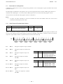
The Main Features of Functions
MCX501 is 1-axis motion control IC which connects to the master CPU with 8-bit or 16-bit bus and can control either a stepper
motor driver or pulse type servo driver for position and speed.
This IC has no multiple of speed (Range Setting) to set the drive speed, that is to say it can freely output the drive speed from 1
pps up to 8 Mpps in increments of 1pps. Acceleration/deceleration driving can perform trapezoidal acceleration/deceleration and
smooth S-curve acceleration/deceleration.
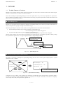
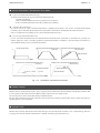
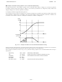
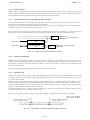
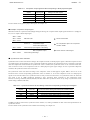
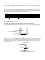
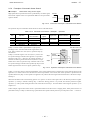
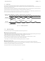
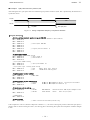
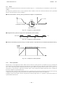
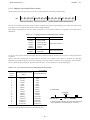
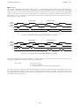
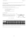
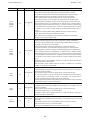
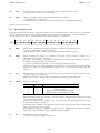
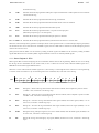
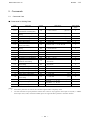
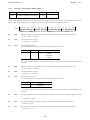
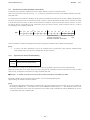
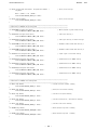
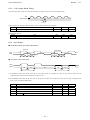
■ Speed Range-Free
MCX501 is a new motion control IC that has no multiple of speed (Range Setting) to set the drive speed. This will enable us to
freely set the speed from 1 pps up to 8 Mpps in increments of 1 pps.
When using the multiples of speed to set the speed by existing method, there are restrictions as described below.
•
For the detaild speed setting of low-speed, less multiples of speed must be set.
→
As a result, driving cannot be shifted to high-speed.
•
To perform the high-speed driving, larger multiples of speed must be set.
→
As a result, the detaild setting of drive speed cannot be configured.
MCX501 brings solutions to the inconvenience described above by Speed range-free, which makes it possible to directly change
the speed from low-speed such as 1 or 2 pps to high-speed such as 1 Mpps during the driving.
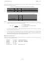
V
High-speed driving without
speed range setting
1,000,000pps
Speed can be set in
increments of 1 pps
Detailed low-speed
setting
163,927pps
7pps
Time
Fig. 1.1-1
Speed Range-Free
■ Easy and High-Accuracy Speed Setting
Since there is no need to set multiples of speed (Range Setting), the user can set a drive speed of output pulses as a speed
parameter (at CLK = 16MHz).
Drive speed (pps)=V×
8,000,000
R
Drive speed (pps) = DV
Acceleration (pps/sec) = AC
Jerk (pps/sec2)
Jerk (pps/sec2) = JK
8,000,000
62.5×10⁶
×
K
R
Speed can be used as a parameter
→ no need to calculate a parameter
・・・
=
・・・
8,000,000
R
Acceleration (pps/sec)=A×125×
Fig. 1.1-2
Speed Parameter Setting
In the range of 1 pps to 8 Mpps, it can output the drive speed that is set with high accuracy. Speed accuracy of the pulse output is
less than ± 0.1%, which is on the assumption that there is no frequency error of input clock (CLK). In fact, there is a frequency
error of input clock (CLK), and speed accuracy depends on it.
- 1 -
MCX501 - 2
NOVA electronics Inc.
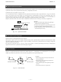
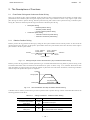
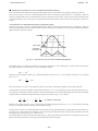
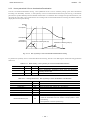
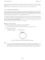
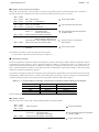
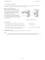
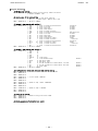
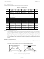
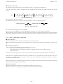
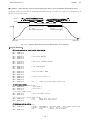
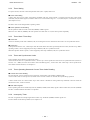
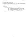
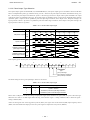
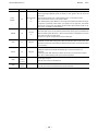
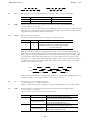
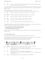
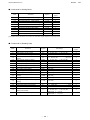
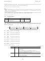
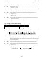
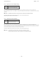
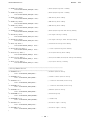
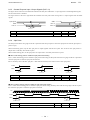
■ Various Acceleration / Deceleration Drive Mode
Types of acceleration/deceleration driving
Acceleration/deceleration driving can perform the following driving.
Constant speed driving
Linear acceleration/deceleration driving (symmetry/non-symmetry)
S-curve acceleration/deceleration driving (symmetry/non-symmetry)
Automatic deceleration start
In position driving of linear acceleration/deceleration (symmetry/non-symmetry) and S-curve acceleration/deceleration
(symmetry), the IC calculates the deceleration start point when in deceleration, and automatically starts deceleration.
(This is not applied to non-symmetry S-curve acceleration/deceleration driving.)
S-curve acceleration/deceleration curve
S-curve acceleration/deceleration uses the method which increases/decreases acceleration or deceleration in a primary line,
and the speed curve forms a secondary parabola acceleration/deceleration. In addition, it prevents triangle waveforms by a
special method during S-curve acceleration/deceleration.
Constant Speed Driving
Trapezoidal Acceleration/Deceleration Driving Trapezoidal Acceleration/Deceleration Driving
(Symmetry)
(Non- Symmetry)
V
V
V
w
Slo
Time
on
ati
ler
ce
c
A
Time
Parabola S- curve Acceleration/Deceleration Driving
(Symmetry)
Rapid Deceleration
Time
Parabola S- curve Acceleration/Deceleration Driving
(Non- Symmetry)
V
V
ow
Sl
P=100000
P=200000
Manual Deceleration
Rapid Acceleration
P=400000
P=50000
Time
Fig. 1.1-3
on
ati
ler
ce
De
Automatic Deceleration
Time
Acceleration / Deceleration Drive Mode
■ Position Control
MCX501 has two 32-bit position counters: one is a logical position counter that counts the number of output pulses and the other
is a real position counter that counts the feedback number of pulses from an external encoder.
The current position can be read by data reading commands anytime.
By using with synchronous action, the operation by the activation factor based on position data, such as a timer starts/stops at a
specified position, can be performed.
■ Software Limit
MCX501 has a software limit function that controls driving to stop when the position counter is over a specified range. There are
2 stop types for when the software limit function is enabled: decelerating stop and instant stop.
- 2 -
MCX501 - 3
NOVA electronics Inc.
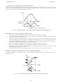
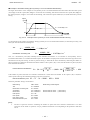
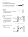
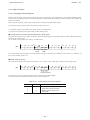
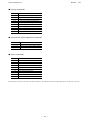
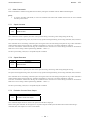
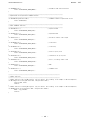
■ Various Synchronous Actions
Synchronous action is the function that executes a specified action together with if a specified activation factor generates. These
synchronous actions can be performed fast and precisely, independent of the CPU.
Synchronous action is possible to set up to 4 sets.
1 set of synchronous actions is configured with one specified activation factor and one specified action. 15 types of activation
factors are provided, such as the passage of a specified position, start/termination of driving, the rising/falling edge of an
external signal and expiring of an internal timer. In addition, 28 types of actions are provided, such as start/termination of
driving, save the current position counter value to multi-purpose register and writing of a drive speed.
Multiple synchronous action sets can be used in combination, which allows users to develop a wide array of applications.
Examples
• Outputs an external signal when passing through a
specified position during the driving.
• Saves the current position to a specified register when
an external signal is input during the driving.
• Outputs N split pulses from a specified position to the
external during the driving.
Action
Output the pulse signal to the external
PIO0
Activation Factor
Axis is passing through the position 15,000
Fig. 1.1-4
Synchronous Action
■ Four Multi-Purpose Registers
MCX501 has four 32-bit length multi-purpose registers.
Multi-purpose register can be used to compare with the current position, speed and timer, and then can read out the status which
represents comparison result and can output as a signal. In addition, it can activate a synchronous action according to comparison
result or can generate an interrupt.
By using with synchronous action, it can save values of the position or current speed during the driving to multi-purpose
registers and load values to parameters from multi-purpose registers.
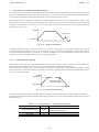
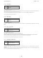
■ Timer Function
MCX501 is equipped with the timer which can set with the range of 1 ~ 2,147,483,647μsec in increments of 1μsec (at CLK =
16MHz). By using with synchronous action, the following operations can be performed precisely.
Timer
V
Time
V
Time
Termination of driving
Next driving stars
After 17.35 msec
Fig. 1.1-5
Timer Function
- 3 -
Examples
• Starts driving after specified periods when the
driving is finished.
• Starts driving after specified periods after an
external signal is input.
• Stops continuous pulse driving after specified
periods.
• Times from position A to position B.
MCX501 - 4
NOVA electronics Inc.
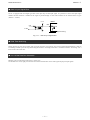
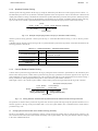
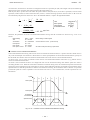
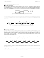
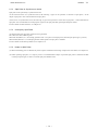
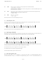
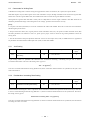
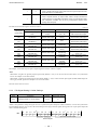
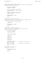
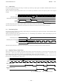
■ Output of Split Pulse
This is a function that outputs split pulses during the driving, which synchronizes axis driving and performs various operations in
the specified intervals.
The split length, pulse width of a split pulse and split pulse number can be set. By using with synchronous action, the output of
split pulses can be started/terminated from a specified position and the split length or pulse width of a split pulse can be changed
by an external signal.
Drive Pulse
1
Split Pulse
2
3
Pulse Width
Split Length
Split Pulse Number
Fig. 1.1-6
Split Pulse Output
■ Automatic Home Search Function
This IC is equipped with the function that automatically executes a home search sequence without CPU intervention. The
sequence comprises high-speed home search → low-speed home search → encoder Z-phase search → offset drive.
Deviation counter clear pulses can be output for a servo motor driver. In addition, the timer between steps which sets stop time
among each step is available, and the operation for a home search of a rotation axis is provided.
■ Servo Motor Feedback Signals
MCX501 has input pins for servo feedback signals such as encoder 2-phase, in-positioning and alarm signals. An output signal
for clearing a deviation counter is also available.
■ Interrupt Signals
Interrupt signals can be generated by various factors. For example, (1). at the start/finish of a constant speed drive during the
acceleration/deceleration driving, (2). at the end of driving, and (3). when the comparison result of a multi-purpose register with
a position counter changes.
■ Driving by External Signals
Driving can be controled by external signals, which are the relative position driving, continuous pulse driving and MPG driving.
This function is used for JOG feed or teaching mode, reducing the CPU load and making operations smooth.
- 4 -
MCX501 - 5
NOVA electronics Inc.
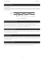
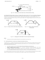
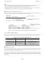
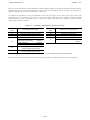
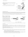
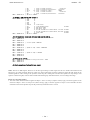
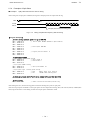
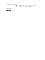
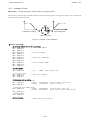
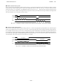
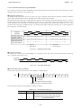
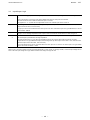
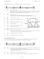
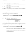
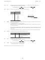
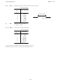
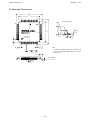
■ Built-in Input Signal Filter
The IC is equipped with an integral type filter in the input step of each input signal. It is possible to set for each input signal
whether the filter function is enabled or the signal is passed through. A filter time constant can be selected from 16 types
(500nsec ~ 16msec).
MCX501
+3.3V
LMTP
+24V
+LIMIT
Built- In Filter (Digital Processing)
Fig. 1.1-7
Built-in Input Signal Filter
■ Real Time Monitoring
During the driving, the current status such as logical position, real position, drive speed, acceleration/deceleration, status of
accelerating/constant speed driving/decelerating/acceleration increasing/acceleration constant/acceleration decreasing and a
timer can be read in real time.
■ 8 or 16 Bits Data Bus Selectable
MCX501 can be connected to either 8-bit or 16-bit CPU.
If 8-bit data bus is used, eight pins which are not used for the data bus can be used as general purpose input signals.
- 5 -
MCX501 - 6
NOVA electronics Inc.
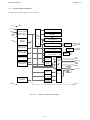
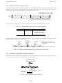
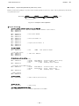
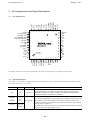
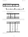
1.2
Functional Block Diagram
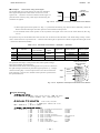
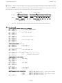
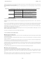
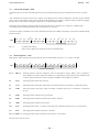
MCX501 functional block diagram is shown as below.
CLK
16MHz
D[15:0]
A[3:0]
CSN
WRN
RDN
INTN
Jerk Generator
Command / Data
Interpretation /
Process Section
Action
Control
Section
Acceleration / Deceleration
Generator
CV
Interrupt
Generator
Speed Generator
P+
P-
Pulse Generator
Automatic Home
Search Section
Logical Position
Counter (32bit)
DOWN
RP
Real Position
Counter (32bit)
DOWN
Parameter・Mode
Setting Register
Synchronous
Action Section
Timer
CT 31bit
UP
Integrated
Filter
A Compare
Multi- Purpose
Register MR3~0
UP
LP
Register
B A:B
Wave
Change
Integrated
Filter
PP/PLS/PA
PM/DIR/PB
ECA/PPIN
ECB/PMIN
Wave
Change
LMTP
LMTM
STOP[2:0]
INPOS
ALARM
EMGN
PIO[7:0]
General Output
OUT[7:0]
Drive
Status Output
Split Pulse
Generator
Synchronous
Pulse /MR
Comparison
A
Selector
B
C
SPLTP
RESETN
Fig. 1.2-1
MCX501 Functional Block Diagram
- 6 -
MCX501 - 7
NOVA electronics Inc.
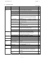
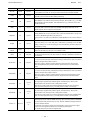
1.3
Specification Table
(CLK=16MHz)
Item
Subitem
Control Axis
Note
1-axis
Data Bus
Drive Pulses
Description
16/8-bit selectable
Drive Speed Range
Output
1 pps ~ 8,000,000 pps
(When CLK=20MHz: up to 10,000,000 pps)
Initial Speed Range
1 pps ~ 8,000,000 pps
Pulse Output Accuracy
± 0.1% or less (according to the setting speed)
Acceleration Range
1 pps/sec ~ 536,870,911pps/sec
Acceleration Increasing/
1 pps/sec ~ 1,073,741,823 pps/sec
2
2
Decreasing Rate Range
Acceleration/Deceleration
Constant speed,
Curve
Symmetrical/non-symmetrical linear acceleration/deceleration,
*1
Symmetrical/non-symmetrical parabola S-curve acceleration/
deceleration
Drive Pulse Range
・Relative position driving : -2,147,483,646 ~ 2,147,483,646
・Absolute position driving : -2,147,483,646 ~ 2,147,483,646
Position Driving
Automatic decelerating stop
Decelerating Stop Mode
Manual decelerating stop
Override
Output pulse number and drive speed are changeable during the
driving
Driving Commands
*2
*3
*4
Relative/Absolute position driving,
+/-direction continuous driving
Triangle Form Prevention
can be used both in linear and S-curve acceleration/deceleration
Drive Pulse Output Type
Independent 2-pulse, 1-pulse 1-direction,
Quadrature pulse and quad edge evaluation,
Quadrature pulse and double edge evaluation are selectable
Encoder Input
Drive Pulse Output Logic
Positive/Negative logical level selectable
Drive Pulse Output Pin
Possible to pin inversion
Input Pulse Input Type
Quadrature pulses input and quad edge evaluation,
Quadrature pulses input and double edge evaluation,
Quadrature pulses input and single edge evaluation,
Up / down pulse input are selectable
Position Counter
Software Limit
Multi-Purpose
Register
Input Pulse Pin
Possible to pin inversion
Logical Position Counter
Count Range: -2,147,483,648 ~ +2,147,483,647
*5
Real Position Counter
Count Range: -2,147,483,648 ~ +2,147,483,647
*5
Variable Ring
Possible to set the count maximu value of each position counter
Setting Range
-2,147,483,648 ~ +2,147,483,647
Stop Mode
Decelerating/Instant stop selectable
Bit Length,
32-bit length
Number of Registers
4 registers
Uses
Compare with position, speed and timer value,
load data such as position and speed, and save data such as
current position, speed and timer value
Timer
Setting Range
Split Pulse
Split Length
2 ~ 65,535 pulses
Split Pulse Width
1 ~ 65,534 pulses
Split Pulse Number
1 ~ 65,535, or up to infinity
Sequence
STEP1 high-speed home search → STEP2 low-speed home search
Deviation Counter Clear
→ STEP3 encoder Z-phase search → STEP4 offset drive
・Enable/Disable each step and search signal/direction are
selectable
Clear pulse width within the range of 10μ ~ 20msec and logical level
Output
is selectable
Timer between Steps
Selectable from 1msec ~ 1,000msec
Automatic Home
Search
1 ~ 2,147,483,647μsec
- 7 -
*6
MCX501 - 8
NOVA electronics Inc.
Synchronous
Number of Sets
4 sets
Action
Activation Factor
・When multi-purpose register comparison changed
*7
・Comparative object: logical/real position counter value,
current drive speed, current timer value
・Comparison condition: ≧,>,=,<
・When a timer is up
・Start/Termination of driving, Start/Termination of
acceleration/deceleration driving at constant speed
・Start/Termination of split pulse, Output of split pulse
・PIOn signal ↑/↓, PIOn+4 signal Low and PIOn signal ↑,
PIOn+4 signal Hi and PIOn signal ↑,
PIOn+4 signal Low and PIOn signal ↓,
PIOn+4 signal Hi and PIOn signal ↓ (n:0,1,2,3)
・Activation command
Action
・Load value (MRn→setting value) - : Drive speed,
Drive pulse number (Finish point), Split length, Split pulse width,
Logical/Real position counter value, Initial speed, Acceleration
・Save value (MRn←current value) : Logical/Real position counter
value, Current timer value, Current drive speed,
Current acceleration
・Synchronous pulse output to the external
・Start of relative/absolute position driving, Start of +/-direction
continuous pulse driving, Start of relative/absolute position driving
at the position set in MRn
・Decelerating stop/Instant stop, Speed increase/decrease,
Timer-start/stop, Start/Termination of split pulse
Interrupt
Repeat
Synchronous action can be operated once/repeatedly.
Interrupt Factor
・When multi-purpose register comparison changed
・Comparative object : logical/real position counter value,
current drive speed, current timer value
・Comparison condition : ≧,>,=,<
・Start/Termination of driving, Start/Termination of
acceleration/deceleration driving at constant speed
・When automatic home search is finished, When a timer is up
・Output/Termination of split pulse,
・When synchronous action 0/1/2/3 is activated
Enable / Disable
Enable/Disable each interrupt factor is selectable
External Signal for
・Relative position/Continuous pulse driving by EXPP, EXPM signals
Driving
・MPG (encoder input : quadrature pulses input and single edge
*8
evaluation)
External Stop
Number of Signals
3 signals (STOP0~2)
Signal
Enable/Disable
Enable/Disable stop signal function is selectable
Logical Level
Low/Hi active is selectable
Stop Mode
*9
When it is active, decelerating stop
(When driving under initial speed, instant stop)
Servo Motor
Signals
Input/Output Signal
Enable/Disable
Enable/Disable a signal is selectable.
Logical Level
Low/Hi active is selectable.
Number of Signals
8 signals
General
Input/Output Signal
ALARM (alarm), INPOS (in-position), DCC (deviation counter clear)
・Synchronous input, pins share the input pin for driving by external
signals.
・Synchronous action output, multi-purpose register comparison
output, pins share drive status output signal pins.
Driving Status
Output Signal
Signals
・Driving, Error, Accelerating, Constant speed driving, Decelerating,
Acceleration increasing, Acceleration constant, Acceleration
decreasing
・Drive status can also be read by status register.
- 8 -
*10
MCX501 - 9
NOVA electronics Inc.
Over Limit Signal
Number of Signals
2 signals (for each + and - direction)
Enable/Disable
Enable/Disable limit function is selectable.
Logical Level
Low/Hi active is selectable.
Stop Mode
Decelerating stop or instant stop is selectable when it is active.
Input Pulse Pin
Possible to pin inversion
Emergency Stop
EMGN 1 point, stop drive pulses output at Low level.
Signal
(Logical level can not be set)
Integral Type Filter
Input Signal Filter
*9
Equipped with integral filters in the input column of each input
signal.
Time Constant
Time constant can be selected from 16 types. (500n, 1μ, 2μ, 4μ, 8μ,
16μ, 32μ, 64μ, 128μ, 256μ, 512μ, 1m, 2 m, 4 m, 8 m, 16 m [sec])
Enable/Disable
Enable/Disable filter function is selectable.
Electrical
Temperature Range for
-40℃~+85℃
Characteristics
Driving
Power Voltage for Driving
+3.3V ±10%
Consumption Current
27mA (average), 44mA (max) at CLK=16MHz
Input Clock Pulse
16MHz (standard) 20MHz (max)
Input Signal Level
TTL level (5V tolerant)
Output Signal Level
3.3V CMOS Level (only TTL can be connected to 5V type)
Package
・64-pin plastic TQFP, pin pitch:0.5mm, RoHS compliant
・Dimension: 10 × 10 × 1.0 mm
<Further Note>
*1
*2
Parameter that is used in S-curve acceleration/deceleration driving.
Pulse range that can be set for the driving that outputs specified pulses.
In continuous pulse driving, pulses are output up to infinity.
Automatic deceleration stop performs decelerating stop automatically by calculating the deceleration start point based on
*3
specified drive pulses. Manual deceleration stop performs decelerating stop by setting the deceleration start point from
the high order. This IC can perform automatic deceleration stop except for non-symmetrical S-curve
acceleration/deceleration.
*4
After the start of driving, output pulse number can be changed for the same direction in only relative position driving.
*5
Logical position counter counts output pulses and real position counter counts encoder input pulses.
*6
While driving, split pulses are output at specified intervals in synchronization with driving pulses.
*7
1 set of synchronous actions is configured with one specified activation factor and one specified action.
*8
Input pins for external signals share the general purpose input/output pins.
*9
When the function is not used, it can be used as general purpose input.
*10
Drive status output signal pins share the general purpose input/output pins.
- 9 -
MCX501 - 10
NOVA electronics Inc.
2. The Descriptions of Functions
2.1
Fixed Pulse Driving and Continuous Pulse Driving
There are two kinds of pulse output commands: fixed pulse driving that is performed based on the number of output pulses
predetermined and continuous pulse driving that outputs pulses until a stop command is issued or stop signal is input. Fixed
pulse driving has relative position driving, absolute position driving and counter relative position driving. Continuous pulse
driving has +direction continuous pulse driving and -direction continuous pulse driving.
•
•
2.1.1
Fixed pulse driving
・ Relative position driving
・ Absolute position driving
・ Counter relative position driving
Continuous pulse driving
・ +Direction continuous pulse driving
・ -Direction continuous pulse driving
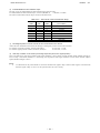
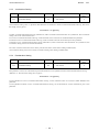
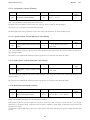
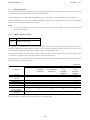
Relative Position Driving
Relative position driving performs the driving by setting the drive pulse number from the current position. To drive from the
current position to the +direction, set the positive pulse number in the drive pulse number, and to the -direction, set the negative
pulse number in the drive pulse number.
To the - direction
20,000 pulses
-direction
To the + direction
20,000 pulses
TP:- 20,000
+direction
TP:+20,000
Current position
Fig. 2.1-1
Setting Example of Drive Pulse Number (TP) in Relative Position Driving
Relative position driving performs constant speed driving or acceleration/deceleration driving. Relative position driving in the
acceleration/deceleration where acceleration and deceleration are equal, as shown in Fig. 2.1-2, automatic deceleration starts
when the number of pulses becomes less than the number of pulses that were utilized at acceleration, and driving terminates
when the output of specified drive pulses is completed.
Speed
Driving Speed
Auto Deceleration
Initial Speed
Stop at specified
Output Pulse
time
Fig. 2.1-2
Auto Deceleration and Stop in Relative Position Driving
Command code for relative position driving is 50h. To perform relative position driving in linear acceleration/deceleration, the
following parameters must be set.
Table 2.1-1
Parameter
Acceleration/Deceleration
Setting Parameters:Relative Position Driving
Symbol
AC/DC
Initial speed
SV
Drive speed
DV
Drive pulse number/
Finish point
TP
Comment
No need to set deceleration when acceleration and
deceleration are equal.
Set +pulse number for the +direction.
Set -pulse number for the -direction.
- 10 -
MCX501 - 11
NOVA electronics Inc.
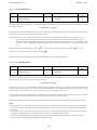
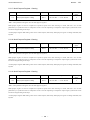
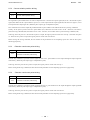
2.1.2
Absolute Position Driving
Absolute position driving performs the driving by setting the destination point based on a home (logical position counter = 0).
The destination point can be set by absolute coordinates regardless of the current position. The IC calculates drive direction and
output pulse number according to the difference between the specified destination point and current position, and then performs
the driving. In absolute position driving, the destination point should be set by absolute coordinates within the range of driving
space. So, the user first needs to perform automatic home search to determine the logical position counter before driving.
-20,000 -10,000
(Home)
0
+10,000
TP:-20,000
+20,000 [Absolute coordinates]
TP:+20,000
Current position
Fig. 2.1-3 Example of Specifying Finish Point (TP) in Absolute Position Driving
Absolute position driving performs constant speed driving or acceleration/deceleration driving as well as relative position
driving.
Command code for absolute position driving is 54h. To perform absolute position driving in linear acceleration/deceleration, the
following parameters must be set.
Setting Parameters :Absolute Position Driving
Table 2.1-2
2.1.3
Parameter
Symbol
Comment
Acceleration/Deceleration
AC/DC
No need to set deceleration when acceleration and
deceleration are equal.
Initial speed
SV
Drive speed
DV
Drive pulse number/
Finish point
TP
Set the destination point by absolute coordinates.
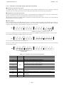
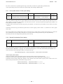
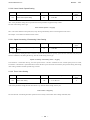
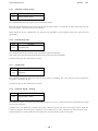
Counter Relative Position Driving
Counter relative position driving performs the driving by setting the direction and drive pulse number to the destination point
based on the current position. Unlike relative position driving, driving is performed in a direction opposite to the sign of the
pulse number that is set in drive pulse number (TP). This is useful for when the user wants to determine a drive direction using a
driving command, by setting the predetermined positive value to the drive pulse number in advance.
If the negative value is set to the drive pulse number, counter relative position driving performs the driving in the +direction.
Drive pulse number(TP)=20,000
To the− direction
20,000 pulses
To the+ direction
20,000 pulses
− direction
+ direction
Counter relative position
Relative position
driving command (51h)
driving command (50h)
Current position
Fig. 2.1-4
Driving Direction is Determined by Relative/Counter Relative Position Driving Command
The operation of counter relative position driving is the same as relative position driving except the operation which drives in a
direction opposite to the sign of the pulse number that is set in drive pulse number (TP). Command code for counter relative
position driving is 51h.
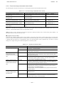
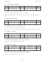
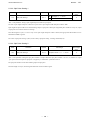
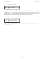
A. Changing Drive Pulse Number in the middle of Driving (Override)
The drive pulse number (TP) can be changed in relative position driving and counter relative position driving. However, the
drive direction must be the same before and after the change of drive pulse number. The drive pulse number cannot be changed
to the value of different direction.
− 11 −
MCX501 - 12
NOVA electronics Inc.
TP:+20,000 in relative position driving
TP changed
-direction
+direction
TP:+30,000
TP:+10,000
TP:-10,000 …NG!
TP in the opposite direction cannot be changed.
Fig. 2.1-5
Override Drive Pulse Number (TP) in Relative Position Driving
In acceleration/deceleration driving, if the rest of output pulses become less than the pulses at acceleration, and the drive
pulse number (TP) is changed during deceleration, the driving accelerates again (Fig. 2.1-7). And if the output pulse number of
changed drive pulse number (TP) is less than the number of pulses already output, the driving stops immediately (Fig. 2.1-8).
In S-curve acceleration/deceleration driving, if the drive pulse number (TP) is changed during deceleration, the S-curve profile
cannot be exactly tracked.
Speed
Speed
Change of Drive Pulse Number
Change of Drive Pulse Number
time
time
Fig. 2.1-6
Change of Drive Pulse Number during Driving
Fig. 2.1-7
Change of Drive Pulse Number
in Deceleration
Speed
Change of
Drive Pulse
Number
time
Fig. 2.1-8
[Note]
•
Changing Drive Pulse Number Less than Output Pulse Number
Absolute position driving cannot change the drive pulse number (TP) while driving.
B. Manual Deceleration for Fixed Pulse Acceleration/Deceleration Driving
As shown in Fig. 2.1-2, generally the deceleration of fixed pulse driving (relative position driving, absolute position driving and
counter relative position driving) is controlled automatically by MCX501. However, in the following situations, it should be
preset the deceleration point by the users.
•
•
•
The change of speed is too often in the trapezoidal acceleration/deceleration fixed pulse driving.
Speed is changed during the driving in the non-symmetry trapezoidal acceleration/deceleration and S-curve
acceleration/deceleration fixed pulse driving.
Acceleration, deceleration, jerk (acceleration increasing rate) and deceleration increasing rate are set individually for
S-curve acceleration/deceleration fixed pulse driving (non-symmetry S-curve acceleration/deceleration).
To set manual deceleration mode, please set D0 bit of WR3 register to 1, and use manual decelerating point setting command
(07h) to set a deceleration point. As to other operations, the setting is the same as those of fixed pulse driving.
- 12 -
MCX501 - 13
NOVA electronics Inc.
C. Offset Setting for Acceleration/Deceleration Driving
The offset function can be used for compensating the pulses when the decelerating speed does not reach the setting initial speed
during acceleration/deceleration fixed pulse driving. MCX501 will calculate the acceleration/deceleration point automatically,
and arrange the output pulses of deceleration phase that is equal to those of acceleration phase.
When setting the offset for deceleration, MCX501 will start deceleration early for the offset. The greater positive value is set for
the offset, the closer the automatic declaration point becomes, for this reason creep pulses of the initial speed will increase at the
termination of deceleration. If a negative value is set for the offset, output may stop prematurely before the speed reaches the
initial speed (see Fig. 2.1-9).
Speed
Offset Pulse
Initial Speed
time
Fig. 2.1-9
Offset for Deceleration
The default value for the offset is 0 when MCX501 power-on reset. It is not necessary to change the shift pulse value in normal
acceleration/deceleration fixed pulse driving. As for fixed driving in non-symmetrical trapezoidal acceleration/deceleration or
S-curve acceleration/deceleration, if creep pulses or premature termination occurs at the termination of driving due to the low
initial speed, correct by setting the acceleration counter offset appropriately.
2.1.4
Continuous Pulse Driving
When continuous pulse driving is performed, MCX501 will drive pulse output in a specific speed until a stop command or
external stop signal becomes active. The user can use it for: home searching, teaching and speed control.
There are two stop commands, one is “decelerating stop” and the other is “instant stop”. And three input pins STOP0 ~ STOP2
can be connected for external decelerating stop (instant stop when driving under initial speed) signal. Enable/disable and active
level can be set in mode setting.
Speed
Drive Speed
Stop Command or
External Stop Signal
Initial Speed
time
Fig. 2.1-10
Continuous Pulse Driving
+ Direction continuous pulse driving command (52h) and - Direction continuous pulse driving command (53h) are available.
To perform acceleration/deceleration continuous pulse driving, parameters except drive pulse number (TP) must be set as well as
fixed pulse driving.
Table 2.1-3
Parameter
Acceleration/Deceleration
Setting Parameters:Continuous Pulse Driving
Symbol
AC/DC
Initial speed
SV
Drive speed
DV
Comment
No need to set deceleration when acceleration
and deceleration are equal.
- 13 -
MCX501 - 14
NOVA electronics Inc.
■ Changing Drive Speed during the Driving (Override)
The drive speed can be changed freely during continuous pulse driving, which can be altered by changing a drive speed
parameter (DV) or issuing a speed increase/decrease command.
In S-curve acceleration/deceleration driving, it will be invalid if the speed is changed in the middle of acceleration/deceleration.
In fixed pulse driving under the symmetry trapezoidal acceleration/deceleration and constant speed, a drive speed (DV) can be
changed during the driving. However, if a speed of fixed pulse driving is changed at linear acceleration/deceleration, some
premature termination may occur. So please note when using the IC with low initial speed.
In fixed pulse driving (automatic deceleration mode) under the non-symmetry trapezoidal acceleration/deceleration and S-curve
acceleration/deceleration, the drive speed cannot be changed during the driving.
<Speed Change by Drive Speed Setting>
If a drive speed parameter (DV) is changed by drive speed setting command (05h), the setting will be immediately applied.
And if during acceleration/deceleration driving, the drive speed increases/decreases to a specified drive speed.
Speed (pps)
40k
30k
25k
DV:30,000 setting
15k
DV:40,000 setting
DV:15,000 setting
time
Fig. 2.1-11
Example of Drive Speed Change during the Driving
<Speed Change by Speed Increase/Decrease Command>
The speed increasing/decreasing value (IV) must be set in advance. If speed increase command (70h) or speed decrease
command (71h) is issued during the driing, the setting will be immediately applied. And if during acceleration/deceleration
driving, the drive speed increases/decreases from the current drive speed to the value of the speed increasing/decreasing value
setting.
Speed increasing / decreasing value (IV)=10,000
Speed (pps)
40k
30k
20k
10k
Speed Decrease
Speed Increase
Speed Decrease
Speed Increase
Speed Decrease
time
Fig. 2.1-12
Example of Speed Change by Speed Increase/Decrease Command
■ Stop Condition for External Input STOP2 to STOP0 in Continuous Pulse Driving
Assign a near home signal, a home signal and an encoder Z-phase signal in STOP0 to STOP2. (Assign an encoder Z phase signal
in STOP2.) Enable/disable and logical levels can be set by WR2 register. If high-speed searching, continuous pulse driving is
performed at acceleration/deceleration. And when the signal that is enabled becomes active, MCX501 will perform decelerating
stop. If low-speed searching, continuous pulse driving is performed at constant speed. And when the signal that is enabled
becomes active, MCX501 will perform instant stop.
This IC has automatic home search function. See Chapter 2.5 for details of automatic home search function.
- 14 -
MCX501 - 15
NOVA electronics Inc.
2.2
Acceleration and Deceleration
There are the following speed curves that can trace from drive pulse output: Constant speed driving which does not perform
acceleration/deceleration, Trapezoidal acceleration/deceleration driving which performs linear acceleration/deceleration to a
setting speed, and S-curve acceleration/deceleration driving which performs acceleration/deceleration to a specified drive speed
with a smooth curve.
And the following acceleration/deceleration driving is each available: Symmetry acceleration/deceleration where acceleration
and deceleration are equal and Non-symmetry acceleration/deceleration where acceleration and deceleration are set individually.
Constant speed driving
Acceleration/Deceleration driving
• Trapezoidal acceleration/deceleration driving
・ linear acceleration/deceleration (Symmetry)
・ Non-symmetry linear acceleration/deceleration
• S-curve acceleration/deceleration driving
・ S-curve acceleration/deceleration (Symmetry)
・ Non-symmetry S-curve acceleration/deceleration
2.2.1
Constant Speed Driving
Constant speed driving outputs drive pulses at a constant speed without acceleration/deceleration. To perform constant speed
driving, the drive speed must be set lower than the initial speed (that is the initial speed is higher than the drive speed.). Constant
speed driving performs the driving at the drive speed lower than the initial speed without acceleration/deceleration. Stop mode is
instant stop.
If the user wants to stop immediately when the home sensor or encoder Z-phase signal is active, perform the low-speed constant
speed driving from the beginning not acceleration/deceleration driving.
Speed
Initial Speed
Drive Speed
time
Fig. 2.2-1
Constant Speed Driving
To perform constant speed driving, the following parameters must be set.
Table 2.2-1
Setting Parameters:Constant Speed Driving
Parameter
Symbol
Initial speed
SV
Drive speed
DV
Drive pulse number /
Finish point
Comment
Set higher than the drive speed (DV).
TP
Not required for continuous pulse driving.
■ Example for Parameter Setting of Constant Speed
The constant speed is set 980 PPS as shown in Fig. 2.2-2 below. In this case, the relative position driving that the drive pulse
number is 2450 is performed.
Speed
(pps)
Initial speed
SV = 980
Drive speed
DV = 980
Drive
TP = 2450
Set the value which initial
speed ≧ Drive speed
980
pulse number
0
Fig. 2.2-2
Please refer each parameter in Chapter 5.2.
- 15 -
2.5
time (sec)
Example of Constant Speed Driving
MCX501 - 16
NOVA electronics Inc.
2.2.2
Trapezoidal Driving [Symmetrical]
In linear acceleration/deceleration driving, the driving accelerates from the initial speed at the start of driving to the drive speed
in a primary linear form with a specified acceleration slope. Linear acceleration/deceleration driving can decelerate
automatically and no need to set a decelerating point. In fixed pulse driving under the symmetry trapezoidal acceleration/
deceleration where acceleration and deceleration are equal, it counts the number of pulses that were utilized at acceleration and
automatic deceleration starts when the rest of output pulses become less than the pulses at acceleration. Deceleration continues in
the primary line with the same slope as that of acceleration until the speed reaches the initial speed, and then driving will stop at
the completion of the output all pulses.
If the decelerating stop command is performed during acceleration, the driving will start to decelerate during acceleration, as
show in Fig. 2.2-3.
Speed
Drive Speed
Deceleration = Acceleration
Acceleration (slope)
Decelerating stop is
performed during acceleration
Initial Speed
time
Fig. 2.2-3
Trapezoidal Driving (Symmetry)
To perform symmetry linear acceleration/deceleration driving using automatic deceleration, bits D2 to 0 of WR3 register and the
following parameters must be set.
Table 2.2-2
Mode Setting:Linear Acceleration/Deceleration (Symmetry)
Mode Setting Bit
Symbol
Setting
WR3/D0
MANLD
0
Automatic deceleration
WR3/D1
DSNDE
0
When in deceleration, acceleration setting value is used (symmetry).
WR3/D2
SACC
0
Linear acceleration/deceleration
Table 2.2-3
Comment
Setting Parameters:Linear Acceleration/Deceleration (Symmetry)
Parameter
Symbol
Comment
Acceleration
AC
When in deceleration, this value is used to decelerate.
Initial speed
SV
Drive speed
DV
Drive pulse number/Finish point
TP
Not required for continuous pulse driving.
■ Example for Parameter Setting of Trapezoidal Driving
As shown in the figure right hand side, acceleration is formed from the initial speed 500 PPS to 15,000 PPS in 0.3 sec.
Acceleration
AC = 48333
Speed
(pps)
(15000-500)/0.3
= 48333pps/sec
Initial speed
SV = 500
Drive speed
DV = 15000
15,000
500
Please refer each parameter in Chapter 5.2.
0.3
Fig. 2.2-4
- 16 -
time (sec)
Example of Trapezoidal Driving
(Symmetry)
MCX501 - 17
NOVA electronics Inc.
■ Triangle Form Prevention of Trapezoidal Driving (Fixed Pulse Driving)
The triangle form prevention function prevents a triangle form in linear acceleration/deceleration fixed pulse driving even if the
number of output pulses does not reach the number of pulses required for accelerating to a drive speed. The triangle form
indicates the speed curve that shifts to deceleration during the acceleration phase in linear acceleration/deceleration driving.
When the number of pulses that were utilized at acceleration and deceleration exceeds 1/2 of the total number of output pulses
during acceleration, this IC stops acceleration and keeps that driving speed and then decelerates automatically. Therefore, even if
the number of output pulses is less in fixed pulse driving, 1/2 of the number of output pulses becomes constant speed area and
can make the triangle form into the trapezoidal form.
Speed
Accelerating
Stop
P = 2×(Pa+Pd)
P :Output pulse number in fixed driving
Pa:Number of pulses utilized at acceleration
Pd:Number of pulses utilized at deceleration
Pa Pa+Pd Pd
time
Fig. 2.2-5
Triangle Prevention of Linear Acceleration Driving
The triangle form prevention function in linear acceleration/deceleration fixed pulse driving is enabled from a reset. And it can
be disabled by setting D13 bit of WR3 register to 1.
If the decelerating stop command is performed during acceleration, the triangle form prevention does not work. As shown in Fig.
2.2-3, deceleration starts from when the decelerating stop is performed.
2.2.3
Non-Symmetrical Trapezoidal Acceleration
If an object is to be moved using stacking equipment, there will be a need to change acceleration and deceleration of vertical
transfer since gravity acceleration is applied to the object.
This IC can perform automatic deceleration in non-symmetrical linear acceleration/deceleration fixed pulse driving where
acceleration and deceleration are different. It is not necessary to set a manual deceleration point by calculation in advance. Fig.
2.2-6 shows the case where the deceleration is greater than the acceleration and Fig. 2.2-7 shows the case where the acceleration
is greater than the deceleration. In such non-symmetrical linear acceleration, the automatic deceleration start point is calculated
by the IC based on the number of output pulses in fixed pulse driving and each rate parameter.
Speed
(pps)
Drive Speed
DV = 30k
Deceleration Rate
DC = 145kpps/sec
Acceleration Rate
AC = 36.25kpps/sec
Initial Speed
SV = 1k
0.8
Fig. 2.2-6
1.2
1.4 time (sec)
Non-Symmetrical Linear Acceleration Driving (acceleration<deceleration)
Speed
(pps)
Drive Speed
DV = 30k
Acceleration Rate
AC = 145kpps/sec
Deceleration Rate
DC = 36.25kpps/sec
Initial Speed
SV = 1k
0.2
Fig. 2.2-7
0.6
1.4 time (sec)
Non-Symmetrical Linear Acceleration Driving (acceleration>deceleration)
- 17 -
MCX501 - 18
NOVA electronics Inc.
To perform non-symmetry linear acceleration/deceleration driving using automatic deceleration, bits D2 to 0 of WR3 register
and the following parameters must be set.
Table 2.2-4
Mode Setting : Non-symmetry Linear Acceleration/Deceleration
Mode Setting Bit
Symbol
Setting
WR3/D0
MANLD
0
WR3/D1
DSNDE
1
When in deceleration, deceleration setting value is used.
WR3/D2
SACC
0
Linear acceleration/deceleration
Table 2.2-5
Setting Parameters : Non-symmetry Linear Acceleration/Deceleration
Parameter
[Note]
•
Comment
Automatic deceleration
Symbol
Acceleration
AC
deceleration
DC
Initial speed
SV
Drive speed
DV
Drive pulse number/Finish point
TP
Comment
Not required for continuous pulse driving.
In non-symmetry linear acceleration/deceleration driving, when acceleration > deceleration (Fig. 2.2-7), the following
condition is applied to the ratio of acceleration and deceleration.
DC > AC ×
DV
8 × 10 6
DC:Deceleration (pps/sec)
AC:Acceleration (pps/sec)
When CLK = 16MHz
DV:Drive speed (pps)
For instance, if the driving speed DV = 100kps, deceleration D must be greater than 1/80 of acceleration A. The value
must not be less than 1/80 of acceleration.
•
In non-symmetry linear acceleration/deceleration driving, if acceleration > deceleration (Fig. 2.2-7), the greater the
ratio of acceleration AC to deceleration DC becomes, the greater the number of creep pulses becomes (about
maximum of 10 pulses when AC/DC=10 times). When creep pulses cause a problem, solve the problem by increasing
the initial speed or setting a minus value to the acceleration counter offset.
■ Example of Parameter Setting
As shown in Fig. 2.2-6, parameter setting of relative position driving in non-symmetrical linear acceleration/deceleration
(acceleration < deceleration) is shown below.
Mode setting
WR3←0002h
Mode setting of WR3 register
Acceleration
AC = 36250
(30000-1000)/0.8 = 36250pps/sec
Deceleration
DC = 145000
(30000-1000)/0.2 = 145000pps/sec
Initial speed
SV = 1000
Drive speed
DV = 30000
Drive pulse number
TP = 27500
Relative position driving
- 18 -
MCX501 - 19
NOVA electronics Inc.
2.2.4
S-curve Acceleration/Deceleration Driving [Symmetrical]
S-curve acceleration/deceleration driving performs acceleration and deceleration to a specified drive speed with a smooth curve
that forms a secondary parabolic curve.
This IC creates an S-curve by increasing/decreasing acceleration/deceleration in a primary line at acceleration and deceleration
of a drive speed.
Fig. 2.2-8 shows the operation of S-curve acceleration/deceleration driving where acceleration and deceleration are symmetrical.
Section a.
When driving starts, the acceleration increases on a straight line at a specified jerk. In this case, the speed data
forms a quadratic curve.
Section b. If the difference between a specified drive speed and the current speed becomes less than the speed that was
utilized at acceleration increasing, the acceleration starts to decrease on a straight line at a specified jerk.
The decrease ratio is the same as the increase ratio.
In this case, the rate curve forms a parabola of reverse direction.
Section c. When the speed reaches a specified drive speed or the acceleration reaches 0, the driving keeps that speed.
In fixed pulse driving of S-curve acceleration/deceleration where acceleration and deceleration are symmetrical,
when the rest of output pulses becomes less than the number of pulses that were utilized in accelerating,
deceleration starts (automatic deceleration).
Section d,e. Also in deceleration, the speed forms a S-curve by increasing/decreasing deceleration in a primary linear form.
The same operation is performed in acceleration/deceleration where the drive speed is changed during continuous pulse driving.
However, In S-curve acceleration/deceleration driving, change of a drive speed during acceleration/deceleration is invalid.
Speed
a
b
c
d
e
Drive Speed
Initial Speed
time
Acceleration
/ Deceleration
Acceleration increasing rate (slope)
Acceleration
Deceleration
time
Fig. 2.2-8
S-curve Acceleration/Deceleration Driving (Symmetry)
To perform symmetry S-curve acceleration/deceleration driving by using automatic deceleration, bits D2 to 0 of WR3 register
and the following parameters must be set.
Table 2.2-6
Mode Setting:S-curve Acceleration/Deceleration (Symmetry)
Mode Setting Bit
Symbol
Setting
WR3/D0
MANLD
0
Automatic deceleration
WR3/D1
DSNDE
0
When in deceleration, acceleration and jerk setting values are used.
WR3/D2
SACC
1
S-curve acceleration/deceleration
Table 2.2-7
Comment
Setting Parameters:S-curve Acceleration / Deceleration (Symmetry)
Parameter
Symbol
Jerk
JK
Acceleration
AC
Initial speed
SV
Drive speed
DV
Drive pulse number/Finish point
TP
Comment
Set the maximum value:536,870,911 (1FFF FFFFh).
Not required for continuous pulse driving.
- 19 -
MCX501 - 20
NOVA electronics Inc.
■ Triangle Form Prevention of S-curve Acceleration/Deceleration Driving
S-curve acceleration/deceleration driving also has the triangle form prevention function for keeping a speed curve smooth.
In fixed pulse driving of S-curve acceleration/deceleration where acceleration and deceleration are symmetrical, when the
number of output pulses does not reach the number of pulses required for accelerating to a drive speed or when decelerating stop
is performed during S-curve acceleration, the triangle form prevention function works in both cases and keeps a speed curve
smooth.
<The Prevention of Triangle Driving Profile in Fixed Pulse Driving>
In fixed pulse driving of S-curve acceleration/deceleration where acceleration and deceleration are symmetrical, when the
number of output pulses does not reach the number of pulses required for accelerating to a drive speed, the following method is
applied to keep a speed curve smooth.
Speed
2
3
p(t)
Initial Speed
1
1
3
2
3
1
1
3
time
Acceleration
/ Deceleration
Acceleration
Deceleration
t
Fig. 2.2-9
time
The Rule of 1/12 of S-curve Acceleration/Deceleration
If the initial speed is "0" and the acceleration is increased up to the time "t" at a constant jerk "a", in the section of acceleration
increasing, the speed "v(t)" in the time "t" can be expressed as follows.
v(t) = at 2
Therefore, the total number of pulses “p(t)” utilized during the time from “0” to “t” is the integral of the speed “v(t)” from the
time “0” to “t”.
p(t) =
1
3
× at 3
This value indicates 1/3 of at2×t (the number of pulses of one square on the figure) regardless of the value of the jerk.
In fixed pulse driving, the acceleration is increased from the time “0” to “t” at a specified jerk, and is decreased from the time “t”
at the same jerk. When the acceleration reaches 0, and if the deceleration is also increased/decreased at the same jerk, the number
of pulses that were utilized in fixed pulse driving is expressed, as shown in Fig. 2.2-9, as follows.
1
2
2
1
+
+ 1 + 1 +
+
3
3
3
3
= 4 squares on the figure
Therefore, the number of pulses (1/3 of a square) that were utilized during the time from “0” to “t” in acceleration increasing
section is 1/12 of pulses that were utilized in all fixed pulse driving.
For this reason, in S-curve acceleration/deceleration fixed pulse driving, when the number of output pulses during acceleration is
more than 1/12 of total output pulses, MCX501 will stop increasing acceleration and start to decrease the acceleration value with
the speed curve as shown in Fig. 2.2-9. [Rule of 1/12]
This method makes an ideal curve when the initial speed is 0, however the initial speed cannot be 0, so the pulses from 0 on the
figure to the initial speed will be excess and will be output at the peak of the speed.
- 20 -
MCX501 - 21
NOVA electronics Inc.
<The Prevention of Triangle Driving Profile in Decelerating Stop>
In linear acceleration/deceleration driving, if the decelerating stop is commanded during acceleration, the speed curve forms a
triangle form. In S-curve acceleration/deceleration driving, if the decelerating stop is commanded during acceleration as shown
in Fig. 2.2-10, deceleration starts after the acceleration reaches 0.
Speed
time
②Decrease the Acceleration value
Acceleration
/ Deceleration
①Request for Deceleration Stop
time
③Deceleration starts when Acceleration becomes 0
Fig. 2.2-10
Triangle Prevention of S-curve Acceleration/Deceleration by Decelerating Stop
■ Constraints for S-curve Acceleration/Deceleration Driving
a.
b.
c.
d.
The drive speed cannot be changed during S-curve acceleration/deceleration fixed pulse driving.
In S-curve acceleration/deceleration fixed pulse driving, if the drive pulse number is changed during deceleration, the
S-curve profile cannot be exactly tracked.
In S-curve acceleration/deceleration fixed pulse driving, if an extremely low value is set as the initial speed, premature
termination (output of specified driving pulses is completed and terminated before the speed reaches the initial speed) or
creep (output of specified driving pulses is not completed even if the speed reaches the initial speed and the rest of
driving pulses is output at the initial speed) may occur in decelerating.
The drive speed can be changed during S-curve acceleration/deceleration continuous pulse driving.
However, the command to change the drive speed during acceleration/deceleration will be invalid.
To change the speed in S-curve acceleration/deceleration continuous pulse driving, make sure to change it during
constant speed driving (RR0 register CNST=1).
Speed increase/decrease (70h, 71h) commands and speed change by synchronous action will also be invalid.
■ Example of Parameter Setting (Symmetry S-Curve Acceleration/Deceleration)
The figure shown below is the example of S-curve acceleration that reaches from the initial speed 100pps to the drive speed
40kpps in 0.4 seconds.
Speed
DV
DV-SV
2
DV-SV
2
SV
Acceleration
time
JK(slope)
DV-SV
2
t
2
Fig. 2.2-11
t = 0.4sec
time
Example of Symmetry S-Curve Acceleration/Deceleration Driving
- 21 -
MCX501 - 22
NOVA electronics Inc.
At acceleration, acceleration is increased on a straight line based on a specified jerk (JK). The integral value (area indicated by
diagonal lines) is the increased value of the speed from the initial speed “SV”.
Find the jerk (JK) to produce the result where the speed reaches a half ((DV-SV)/2) of the drive speed (DV) from the initial
speed (SV) within a half (t/2) of the acceleration time (t=0.4sec). Use the following expression to find a value of “JK” since the
area indicated by diagonal lines which uses “JK” in the left-hand member, is equal to the right-hand member.
1
2
⎛ t ⎞
⎟⎟
× JK × ⎜⎜
⎝ 2 ⎠
JK =
JK =
2
DV − SV
2
=
4(DV − SV)
t2
4(40000 − 100)
JK [pps/sec2]
DV [pps]
SV [pps]
t [sec]
Jerk
Drive speed
Initial speed
Acceleration time
2
= 997,500 pps/sec
0.4 2
Therefore, the parameters for S-curve acceleration/deceleration driving with the acceleration as shown in Fig. 2.2-11 are as
follows.
Mode Setting
WR3 ← 0004h
Jerk
JK = 997500
Mode setting of WR3 register
Acceleration
AC = 536870911
Initial speed
SV = 100
Drive speed
DV = 40000
Drive pulse number
TP = 27500
Set the maximum value:(1FFF FFFFh)
Set when fixed pulse driving is performed.
■ Partial S-curve Acceleration/Deceleration
In acceleration/deceleration driving with a linear section of acceleration and deceleration, it is possible to form a smooth S-curve
only in the start/end part of acceleration or deceleration. To set the speed parameter for acceleration and deceleration, specify not
the maximum value but the value of acceleration and deceleration in a linear section of acceleration/deceleration.
As shown in Fig. 2.2-12, section b,f indicate a linear section of acceleration/deceleration and section a,c,e,g indicate S-curve
section of acceleration/deceleration.
At section a, the acceleration increases on a straight line from 0 to the acceleration setting value and the speed curve forms a
secondary parabolic curve. When the acceleration reaches the acceleration setting value, the acceleration keeps that value and the
speed curve forms a straight line in the acceleration of section b. If the difference between a specified drive speed and the current
speed becomes less than the speed that was utilized at acceleration increasing, the acceleration starts to decrease at a specified
jerk and the speed curve forms a parabola of reverse direction at section c. Also in deceleration, it forms a partial S-curve of
deceleration.
Speed
a
b
c
d
e
f
g
Drive Speed
Initial Speed
Acceleration
/ Deceleration
time
Acceleration increasing rate (slope)
Specified Value
Acceleration
Deceleration
time
Fig. 2.2-12
Partial S-curve Acceleration/Deceleration Driving
- 22 -
MCX501 - 23
NOVA electronics Inc.
■ Example of Parameter Setting (Partial S-curve Acceleration/Deceleration)
The figure shown below is the example of partial S-curve acceleration that reaches to 10kpps in 0.2 seconds by parabolic
acceleration and then reaches from 10kpps to 30kpps in 0.2 seconds by acceleration on a straight line, finally reaches from
30kpps to 40kpps in 0.2 seconds by parabolic acceleration.
To simplify a calculation, suppose the initial speed is 0.
The acceleration increases to the first 10kpps in 0.2 seconds by straight line on a parabolic acceleration, and this integral value
(area indicated by diagonal lines) corresponds to the rising speed 10kpps of the first parabolic acceleration. Therefore, the
acceleration at 0.2 seconds is 10k×2/0.2=100kpps/sec and the jerk is 100k/0.2=500kpps/sec2.
Speed
(pps)
40k
30k
10k
0
0.2
0.4
0.6
time (sec)
0.2
0.4
0.6
time (sec)
Acceleration
(pps/sec)
100k
10kpps
0
Fig. 2.2-13
Example of Partial S-curve Acceleration/Deceleration Driving
However the initial speed cannot be 0, the initial speed SV must be set the value larger than 0. In partial S-curve acceleration/
deceleration, the initial speed SV should be the value more than a square root of acceleration AC.
Thus, with the acceleration as shown in Fig. 2.2-13, parameter setting of partial S-curve acceleration/deceleration driving is
shown below.
Mode setting
WR3 ← 0004h
Mode setting of WR3 register
Jerk
JK = 500000
Set jerk for the section of parabolic acceleration (S-curve).
Acceleration
AC = 100000
Set Acceleration for the section of linear acceleration.
Initial speed
SV = 400
Drive speed
DV = 40000
Drive pulse number
TP = 40000
Set when fixed pulse driving is performed.
- 23 -
MCX501 - 24
NOVA electronics Inc.
2.2.5
Non-symmetrical S-Curve Acceleration/Deceleration
In S-curve acceleration/deceleration driving, a non-symmetrical S-curve can be created by setting a jerk and a deceleration
increasing rate individually. However, in non-symmetry S-curve acceleration/deceleration fixed pulse driving, a deceleration
point must be specified manually because automatic deceleration is not available. Since a triangle form prevention function (1/12
rule) does not work either, a drive speed must be set according to the acceleration/deceleration increasing rate and the number of
output pulses for fixed pulse driving.
Speed
Drive Speed
Initial Speed
time
Acceleration
/ Deceleration
Acceleration increasing rate (JK)
Deceleration increasing rate (DJ)
Acceleration
Deceleration
time
Fig. 2.2-14
Non-symmetry S-Curve Acceleration/Deceleration Driving
To perform non-symmetry S-curve acceleration/deceleration driving, bits D2 to 0 of WR3 register and the following parameters
must be set.
Table 2.2-8
Mode Setting:Non-symmetry S-curve Acceleration/Deceleration
Mode Setting Bit
Symbol
Setting
WR3/D0
MANLD
1
WR3/D1
DSNDE
1
WR3/D2
SACC
1
Table 2.2-9
Comment
Manual deceleration
When in deceleration, deceleration setting value and deceleration
increasing rate are used.
S-curve acceleration/deceleration
Setting Parameters:Non-symmetry S-curve Acceleration / Deceleration
Parameter
Symbol
Jerk
JK
Deceleration increasing rate
DJ
Comment
Acceleration
AC
Set the maximum value: 536,870,911 (1FFF FFFFh)
Deceleration
DC
Set the maximum value: 536,870,911 (1FFF FFFFh)
Initial speed
SV
Drive speed
DV
Drive pulse number/Finish point
TP
Not required for continuous pulse driving.
・Set the value calculated by subtracting the number of pulses that were
Manual deceleration point
DP
utilized at deceleration from the number of output pulses in fixed
pulse driving.
・ Not required for continuous pulse driving.
- 24 -
MCX501 - 25
NOVA electronics Inc.
■ Example of Parameter Setting (Non-symmetry S-curve Acceleration/Deceleration)
The figure shown below is the example of non-symmetry S-curve acceleration/deceleration that reaches from the initial speed
(SV) 100pps to the drive speed (DV) 40kpps in 0.2 seconds in accelerating, and decreases from the drive speed (DV) 40kpps to
the initial speed (SV) 100pps in 0.4 seconds in decelerating. This is that drive pulse number (TP) is 20,000 and relative position
driving.
Speed
(pps)
40K
DJ = 0.9975 Mpps/sec2
JK = 3.99 Mpps/sec2
100
0.2
Fig. 2.2-15
0.4
time (sec)
Example of Non-symmetry S-Curve Acceleration/Deceleration Driving
Use the formula of the example of parameter setting (symmetry S-curve acceleration/deceleration) as described previously, and
find a jerk and a deceleration increasing rate.
Jerk
JK =
4(40000 − 100)
= 3.99 Mpps/sec2
0.22
DJ =
Deceleration increasing rate
4(40000 − 100)
= 0.9975 Mpps/sec2
0.42
Next, set a deceleration point (DP) manually because automatic deceleration is not available in non-symmetry S-curve
acceleration/deceleration. As a manual deceleration point, set the number of output pulses from the start of driving to the start of
deceleration in fixed pulse driving. In relative position driving, it should be the value calculated by subtracting the number of
pulses (Pd) that were utilized at deceleration from the number of drive pulses (TP), so first, find the number of pulses (Pd) that
were utilized at deceleration.
Pulses utilized at deceleration
Pd = (DV + SV)
DV − SV
DJ
= (40000 + 100)
40000 − 100
0.9975 × 10 6
= 8020
If the number of pulses (Pd) that were utilized at deceleration is 8,020 where the number of drive pulses (TP) is 20,000 in
relative position driving, the manual deceleration point will be as follows.
Manual deceleration point
DP = TP – Pd = 20000 – 8020 = 11980
Therefore, parameter setting is shown below.
[Note]
•
Mode setting
WR3←0007h
Jerk
JK = 3990000
Deceleration increasing rate
DJ = 997500
Acceleration
AC = 536870911
Set the maximum value: (1FFF FFFFh)
Deceleration
DC = 536870911
Set the maximum value: (1FFF FFFFh)
Initial speed
SV = 100
Drive speed
DV = 40000
Drive pulse number
TP = 20000
Manual deceleration point
DP = 11980
Mode setting of WR3 register
The above expression used for calculating the number of pulses that were utilized at deceleration is an ideal
expression. In the actual IC operation, creep or premature termination occurs depending on the parameter values that
are set.
- 25 -
MCX501 - 26
NOVA electronics Inc.
2.2.6
Pulse Width and Speed Accuracy
■ Duty Ratio of Drive Pulse
The period time of +/- direction pulse driving is decided by system clock SCLK. The tolerance is within ±1CLK (At
CLK=16MHz, the tolerance is ±62.5nsec). Basically, the duty ratio of each pulse is 50% as shown below. When the parameter
setting is DV = 1000pps, the driving pulse is 500μsec on its Hi level and 500μsec on its Low level and the period is 1.00 msec.
SV = 1000
DV = 1000
500μsec
500μsec
1.00 msec
Fig. 2.2-16
Hi/Low Level Width of Driving Pulse Output (1000pps)
In acceleration/deceleration driving, the Low level pulse width is smaller than that of Hi level pulse during the acceleration; the
Low level pulse is larger than that of Hi level pulse during the deceleration since the drive speed is increasing during outputting
one drive pulse.
Acceleration Area
tLA
tHA
tHA > tLA
Fig. 2.2-17
Constant Speed Area
Deceleration Area
tHC
tLC
tHC = tLC
tHD
tLD
tHD < tLD
Comparison of Drive Pulse Width in Acceleration / Deceleration
■ The Accuracy of Drive Speed
The circuits to generate drive pulses on MCX501 operate with input clock (CLK). If CLK input is standard 16MHz, the user had
better drive the pulse speed in an exact multiple of CLK period (62.5nsec). However, in this case the frequency (speed) of
driving pulse can only be generated by an exact multiple of CLK. For instance, double: 8.000 MHz, triple: 5.333 MHz,
quadruple: 4.000 MHz, five times: 3.200 MHz, six times: 2.667 MHz, seven times: 2.286 MHz, eight times: 2.000 MHz, nine
times: 1.778 MHz, ten times: 1.600 MHz, ······. Any fractional frequencies cannot be output. Therefore, MCX501 uses the
following method to output any drive speed.
For instance, in the case of the drive speed DV = 980kpps, since this period is not an integral multiple of CLK period, pulses of
980kpps cannot be output under a uniform frequency. Therefore, as shown in the figure below, MCX501 combines 16 times and
17 times of CLK period in a rate of 674:326 to generate an average 980kpps.
16
16
16
Fig. 2.2-18
17
16
16
17
The Driving Pulse of 980kpps
According to this method, MCX501 can generate a constant speed driving pulse in a very high accuracy. And speed accuracy of
pulse output is ± 0.1% or less,
Using oscilloscope for observing the driving pulse, we can find the jitter about 1CLK (62.5nsec). This is no matter when putting
the driving to a motor because the jitter will be absorbed by the inertia of motor system.
- 26 -
MCX501 - 27
NOVA electronics Inc.
2.3
Position Control
MCX501 has two 32-bit up-and-down counters for controlling the current position (logical position counter and real position
counter), which can compare with the current position by presetting a value to a multi-purpose register. In addition, the software
limit function and variable ring function can be set to the logical and real position counters.
2.3.1
Logical Position Counter and Real position Counter
The logical position counter counts driving pulses in MCX501. When one +direction pulse is output, the counter will count up 1,
and when one -direction pulse is output, the counter will count down 1.
The real position counter counts input pulse numbers from external encoder. The type of input pulse can be selected from either
quadrature pulses type or Up/Down pulse type. (See Chapter 2.12.3)
Host CPU can read or write these two counters anytime. The counting range is between -2,147,483,648 ~ +2,147,483,647 and 2's
complement is used for negative numbers. The values of the logical and real position counters are undefined at reset.
Waveform
change
Read / Write
Logical Position Counter UP
32bit
DOWN
Read / Write
Real Position Counter
32bit
Fig. 2.3-1
2.3.2
UP
Waveform
change
DOWN
PP/PLS/PA
Driving output pulse
PM/DIR/PB
ECA/PPIN
Encoder input pulse
ECB/PMIN
Position Counter Functional Block Diagram
Position Comparison
MCX501 has four multi-purpose registers, which can be used to compare with the current position of the logical and real
position counters. The comparison result of a multi-purpose register with the logical/real position counter can be read out even
while driving. And when it meets the comparison condition, a signal can be output, or an interrupt or synchronous action
activation can be executed.
For more details of the multi-purpose register comparison functions, see Chapter 2.4.
2.3.3
Software Limit
Software limit can be set to the logical position counter and real position counter. The object of software limit can be set by D14
bit of WR2 register. Two 32-bit registers (SLMT+, SLMT-) which set the software limit must be set the software limit position
of +/- direction individually.
When the value of the logical/real position counter that the software limit is set is larger than the value of SLMT+ register,
decelerating stop or instant stop is executed and D0 bit of RR2 register becomes 1. This error status will be cleared when the
-direction driving command is executed and the value of the logical/real position counter is smaller than the value of SLMT+
register. It is the same with the SLMT- register of -direction.
In +direction software limit, if “position counter≧SLMT+ value”, software limit error occurs. In -direction software limit, if
“position counter<SLMT- value”, software limit error occurs.
Fig. 2.3-2 is the example of SLMT+ register = 10000, SLMT- register = -1000 and software limit function is enabled.
SLMT+ register SP=10000
SLMT- register SM=-1000
SP
+direction software limit error
Current position ≧ SP
-direction software limit error SM
Current position < SM
-1000 0
Fig. 2.3-2
+10000
Value Setting of Software Limit and Software Limit Error
- 27 -
MCX501 - 28
NOVA electronics Inc.
Software limit function can be enabled/disabled by setting D13 bit of WR2 register. And there are two stop types of software
limit, decelerating stop and instant stop, which sets D15 bit of WR2 register. SLMT+ and SLMT- registers can be written
anytime.
Software limit function will be disabled and the values of SLMT+ and SLMT− registers will be undefined at reset.
2.3.4
Position Counter Variable Ring
A logical position counter and a real position counter are 32-bit up/down ring counters. Therefore, normally, when the counter
value is incremented in the +direction from FFFF FFFFh which is the maximum value of the 32-bit length, the value is reset to 0.
When the counter value is decremented in the -direction from 0, the value is reset to FFFF FFFFh. The variable ring function
enables the setting of any value as the maximum value. This function is useful for managing the position of the axis in circular
motions that return to the home position after one rotation, rather than linear motions.
The variable ring size, that is the maximum value of the logical/real position counter can be set to any value within the range of
1~2,147,483,647 (1~7FFF FFFFh). To use the variable ring function, set the logical position counter maximum value (LX) by
logical position counter maximum value setting command (0Eh) and set the real position counter maximum value (RX) by real
position counter maximum value setting command (0Fh).
The value of the logical position counter maximum value (LX) and real position counter maximum value (RX) will be FFFF
FFFFh at reset. When not using the variable ring function, leave it at default.
■ Example of Variable Ring Setting
For instance, set as follows for a rotation axis that rotates one cycle with 10,000 pulses.
① Set 9,999 (270Fh) in the logical position counter maximum value (LX).
② Set 9,999 (270Fh) in the real position counter maximum value (RX) also if using a real position counter.
The count operation will be as follows.
・
Increment in the +direction : …→9998→9999→0→1→…
・
Decrement in the -direction : …→1→0→9999→9998→…
9999 0 1 2
9998
-
+
5000
Fig. 2.3-3
[Note]
•
•
Operation of Position Counter Ring Maximum Value 9999
It is possible to set the value within the range of 1~2,147,483,647 (1~7FFF FFFFh) as the maximum value of the
variable ring function. The signed negative value (8000 0000h~FFFF FFFEh) of a 32-bit register cannot be set.
When setting values to the logical position counter (LP) and real position counter (RP), the values out of the range of
the logical position counter maximum value (LX) and the real position counter maximum value (RX) cannot be set.
- 28 -
MCX501 - 29
NOVA electronics Inc.
2.4
Multi-Purpose Register
MCX501 has four signed 32-bit multi-purpose registers (MR3~0).
Multi-purpose register can be used to compare with the current position, speed and timer, and then can read out the status which
represents comparison result and can output as a signal. In addition, it can activate a synchronous action according to comparison
result and can generate an interrupt. As an action of a synchronous action, it can load the values pre-set in multi-purpose
registers as a new speed or drive pulse number, and can save the current position or speed in multi-purpose registers.
Multi-purpose registers can be written/read anytime, by using each multi-purpose register setting command (10h~13h) and
multi-purpose register reading command (34h~37h).
The values of multi-purpose registers are undefined at reset.
2.4.1
Comparative Object and Comparison Condition
As the comparative objects of multi-purpose registers (MR3~0), the values of the logical position counter, real position counter,
current drive speed and timer can be set. The comparison condition expression to the comparative object can be selected from ≧,
>, =, <.
Read / Write
Logical Position Counter
32bit
Read / Write
Real Position Counter
32bit
Read
Current Speed
Read
Current Timer
31bit
Fig. 2.4-1
Compare
Multi- Purpose Register × 4
MR3~0 32bit
Use of comparison result
・Comparison output signal
・Synchronous action
・Interrupt
Display the comparison result
of large or small
RR4 register/D7~0
Comparison condition
MRn register setting command (20h)
Selector
Read / Write
Comparative object
MRn register setting command (20h)
Multi-Purpose Registers and Compare Function
The user can set the the comparative object and comparison condition to four multi-purpose registers individually by using
multi-purpose register mode setting command (20h). Set specified bits of WR6 data writing register and write multi-purpose
register mode setting command (20h) to WR0 register, and then they will be set.
Multi-purpose register mode setting can be read out by multi-purpose register mode setting reading command (40h).
Multi-purpose register mode setting command (20h)
H
L
D15 D14 D13 D12 D11 D10 D9
D8
D7
D6
D5
D4
D3
D2
D1
D0
M3C1 M3C0 M3T1 M3T0 M2C1 M2C0 M2T1 M2T0 M1C1 M1C0 M1T1 M1T0 M0C1 M0C0 M0T1 M0T0
WR6
MR3
comparison
condition
Table 2.4-1
MR3
comparative
object
MR2
comparison
condition
MR2
comparative
object
Setting of Comparative Object
MR1
comparison
condition
MR1
comparative
object
Table 2.4-2
MnT0 bit
0
0
MRn Comparative Object
MR0
comparative
object
Setting of Comparison Condition
(n:0~3)
MnT1 bit
MR0
comparison
condition
(n:0~3)
MnC1 bit
MnC0 bit
Logical position counter (LP)
0
0
Comparative object ≧ MRn
MRn Comparison Condition
0
1
Real position counter (RP)
0
1
Comparative object > MRn
1
0
Current drive speed value (CV)
1
0
Comparative object = MRn
1
1
Current timer value (CT)
1
1
Comparative object < MRn
- 29 -
MCX501 - 30
NOVA electronics Inc.
[Note]
When the comparative object is set to “current drive speed value (CV)” and comparison condition is set to “comparative
object = MRn”, if the acceleration/deceleration exceeds 4,194,304 (400000h) pps/sec in linear and S-curve
acceleration/deceleration driving, the comparison result may not become TRUE (active).
When the comparative object is “current drive speed value (CV)” and the acceleration/deceleration is more than this value, set
the other conditions such as “comparative object ≧MRn” and not “comparative object =MRn”.
■ Example: Comparison with Logical Position Counter
When the logical position counter value is larger than 500,000 and if the user wants the comparison result is TRUE, set as
follows. In this case, MR0 is used as the register compared with the logical position counter.
WR6 ← A120h
WR7 ← 0007h
Set the value to MR0
MR0:Set 500,000
WR0 ← 0010h
WR6 ← 0000h
WR0 ← 0020h
D3,D2:0,0
Comparison condition : ≧
D1,D0:0,0
Comparative object :
Set comparative object and comparison
Logical position counter (LP)
condition of MR0
Writes multi-purpose register mode setting
[LP<500000]
[LP≧500000]
Comparison condition is not met
→Comparison result :False
400000
Fig. 2.4-2
2.4.2
Comparison condition is met
→Comparison result :True
450000
500000
550000
600000
Comparative object, Condition:
Logical position counter ≧ MR0
MR0:500000
Logical position counter (LP)
Comparison Example of Multi-Purpose Register with Logical Position Counter
Usage of Comparison Result
The user can use the comparison result of comparative object with a multi-purpose register as a comparison output signal,
synchronous action activation and interruption factor. The functions to use the comparison result and actions are as follows.
Table 2.4-3
Usage of Comparison Result and Actions
Function
Object
Comparison output signal
PIO7~4 Output signals
Synchronous action activation
Interruption factor
Synchronous action SYNC3~0
Interrupt function
Action
When comparison result is TRUE, output signal
is Hi.
When comparison result changes to TRUE,
synchronous action is activated.
When comparison result changes to TRUE,
interrupt generates.
■ Comparison Output Signal
The user can output the comparison result of a multi-purpose register as a comparison output signal. When the comparison result
of a multi-purpose register meets a specified comparison condition, the comparison output signal outputs Hi level, and when
does not meet it, the comparison output signal outputs Low level.
The comparison results of multi-purpose registers (MR3~0) are output to each corresponding comparison output signal PIO7~4.
PIO7~4 signals share the other signals such as the general purpose input/output signals. To use them as comparative output pins,
the user needs to set the function of PIO7~4 signals to the comparison output signal by using PIO signal setting 1 command
(21h) in advance.
- 30 -
MCX501 - 31
NOVA electronics Inc.
Table 2.4-4
Comparison output signal and Bit corresponding to Multi-purpose Register
PIO signal setting 1 command (21h)
Multi-purpose
register
Comparison
output signal
MR0
PIO4
WR6/D9 ,8 :1,1
MR1
PIO5
WR6/D11,10:1,1
MR2
PIO6
WR6/D13,12:1,1
MR3
PIO7
WR6/D15,14:1,1
Setting bit of WR6 register
For more details of the general purpose PIO signal, see Chapter 2.8.
■ Example: Comparison Output Signal
When the current drive speed exceeds 5,000pps during the driving, Hi is output to PIO5 output signal and when it is 5,000pps or
less, Low is output to PIO5 output signal.
WR6 ← 1388h
WR7 ← 0000h
Set the value to MR1
MR1:Set 5,000
WR0 ← 0011h
WR6 ← 0060h
D7,D6:0,1
Comparison condition:>
D5,D4:1,0
Comparative object:
Set comparative object and comparison
Current drive speed (CV)
condition of MR1
WR0 ← 0020h
Writes multi-purpose register mode setting
WR6 ← 0C00h
D11,D10:1,1
PIO5 Function:
MR1 comparison output
WR0 ← 0021h
Set the function of PIO5 signal
Writes PIO signal setting 1
■ Synchronous Action Activation
Synchronous action can be activated according to the comparison result of a multi-purpose register. When the comparison result
of a multi-purpose register changes to meet a specified comparison condition, the synchronous action is activated. If it already
meets the comparison condition when the synchronous action is enabled, the synchronous action is not activated at that time.
After it returns to False, if the comparison result of a multi-purpose register again changes to meet a specified comparison
condition, the synchronous action will be activated.
The synchronous action activation according to the comparison result of multi-purpose register MR3~0 can be set as the
activation factor of each corresponding synchronous action set SYNC3~0. To use the comparison result of a multi-purpose
register as the activation factor of a synchronous action, firstly set the activation factor of a synchronous action set which the
user wants to use as “MRn comparison changed to True” (activation factor code:01h) by the synchronous action
SYNC0,1,2,3setting command (26h,27h,28h,29h) and then enable the synchronous action set by using in synchronous action
enable setting command (81h~8Fh).
Table 2.4-5
Synchronous Action Set and Setting Command Corresponding to Multi-purpose Register
Multi-purpose
Register
MR0
Synchronous
Action Set
SYNC0
MR1
SYNC1
Synchronous action SYNC1 setting command (27h)
MR2
SYNC2
Synchronous action SYNC2 setting command (28h)
MR3
SYNC3
Synchronous action SYNC3 setting command (29h)
Synchronous Action Setting Command to set Activation Factor
Synchronous action SYNC0 setting command (26h)
In addition to the activation factor, synchronous action SYNC0,1.2,3 setting commands set other actions and repeat behavior for
synchronous actions.
For more details of the synchronous action functions and settings, see Chapter 2.6.
- 31 -
MCX501 - 32
NOVA electronics Inc.
■ Example: Synchronous Action Activation
While using 10 seconds timer, to activate relative position driving in SYNC2 after 5 seconds from timer-start, set as follows.
The timer activates the synchronous action after 5 seconds from timer-start and is up after 10 seconds.
WR6 ← 4B40h
Set the value to MR2
WR7 ← 004Ch
MR2:Set 5,000,000
WR0 ← 0012h
(5 seconds = 5,000,000μsec)
WR6 ← 9680h
Set10 seconds to the timer value
WR7 ← 0098h
Timer:Set 10,000,000
WR0 ← 0016h
(10 seconds = 10,000,000)
WR6 ← 0300h
D11,D10:0,0 Comparison condition:≧
D9,D8:1,1
Comparative object:
Set comparative object and comparison
Current timer value (CT)
condition of MR2
WR0 ← 0020h
Writes multi-purpose register mode setting
WR6 ← 00A1h
Activation factor code 01h:
MR2 comparison changed to True
Action code 0Ah:Start of relative position driving
Set the function of synchronous
WR0 ← 0028h
Writes synchronous action SYNC2 setting
action SYNS2
WR0 ← 0084h
Synchronous action SYNC2 enable setting
Set to enable SYNC2
command
※ Parameters for relative position driving must be set in advance.
For more details of the relative position driving, see Chapter 2.1.1.
■ Generating an Interrupt
The user can generate an interrupt according to the comparison result of a multi-purpose register. When the comparison result of
a multi-purpose register changes to meet a specified comparison condition, an interrupt generates. If it already meets the
comparison condition when an interrupt is enabled, an interrupt does not generate at that time. After it returns the state not to
meet a specified comparison condition, if the comparison result of a multi-purpose register again changes to meet the specified
comparison condition, an interrupt will generate.
To generate an interrupt according to the comparison result of multi-purpose register MR3~0, the user needs to set each bit of the
interrupt factor of WR1 mode register 1 to enable for the multi-purpose register that is used for comparison. The interrupt factor
of when an interrupt generates can be checked by the interrupt factor check bit of RR1 Status register 1.
Table 2.4-6
Interrupt Enable and Check Bit corresponding to Comparison Result of Multi-purpose Register
Multi-purpose Register
Interrupt Enable Bit
Interrupt Factor Check Bit
MR0
WR1/D0: 1
RR1/D0: 1
MR1
WR1/D1: 1
RR1/D1: 1
MR2
WR1/D2: 1
RR1/D2: 1
MR3
WR1/D3: 1
RR1/D3: 1
For more details of the interrupt, see Chapter 2.10.
■ Example: Interrupt
When the real position counter value is passing through 30,000, an interrupt generates.
WR6 ← 7530h
WR7 ← 0000h
Set the value to MR3
MR3: Set 30,000
WR0 ← 0012h
WR6 ← 0060h
D15,D14:1,0
D13, D12:0,1
Comparison condition:=
Comparative object :
Set comparative object and comparison
Real position counter (RP)
condition of MR3
WR0 ← 0020h
Writes multi-purpose register mode setting
WR1 ← 0008h
Interrupt Factor: Enable MR3 comparison changed to True
- 32 -
Set the interrupt factor
MCX501 - 33
NOVA electronics Inc.
2.4.3
Comparison Result of Large or Small
The comparison result of large or small the multi-purpose register MR3~0 with each comparative object which is set by
multi-purpose register mode setting command (20h) can be checked by RR4 register. Regardless of the comparison condition set
by multi-purpose register mode setting command (20h), it displays the current state.
P≧MRn:Comparative object ≧ MRn, 1
P=MRn:Comparative object = MRn, 1
D15
D14
D13
D12
H
D11
D10
D9
D8
RR4
L
D3
D2
D1
D0
D7
D6
D5
D4
P=MR3 P≧MR3 P=MR2 P≧MR2 P=MR1 P≧MR1 P=MR0 P≧MR0
MR1
MR0
MR3
MR2
Large or Small Large or Small Large or Small Large or Small
According to the bit of RR4 register, the comparison result of large or small the multi-purpose register as follows.
Table 2.4-7
Comparison Result Large or Small and Bit of RR4 register
(n:0~3)
P=MRn(D7,5,3,1)
P≧MRn(D6,4,2,0)
Comparison result with MRn
0
1
comparative object >MRn
x
1
comparative object ≧MRn
1
x
comparative object =MRn
x
0
comparative object <MRn
After the Example: Comparison with Logical Position Counter in 2.4.1 was performed, the bit of RR4 register changes according
to the logical position counter value as shown below.
[LP<500000]
RR4/D1:0
RR4/D0:0
400000
Fig. 2.4-3
2.4.4
[LP=500000]
RR4/D1:1
RR4/D0:1
450000
500000
[LP>500000]
RR4/D1:0
RR4/D0:1
550000
Comparative object, Condition:
Logical position counter ≧ MR0
MR0:500000
600000
Logical position counter (LP)
Example of Comparison Result Large or Small and Bit of RR4 register
Load/Save of Parameters by Synchronous Action
By using the synchronous action, the user can load the value pre-set in a multi-purpose register as a new speed or drive pulse
number, and save the current position and a speed to a multi-purpose register.
Activation Factor
External signal is input
Action
Save the current position
MR0 register
Fig. 2.4-4
-562,490
Usage Example of Saving Parameters
- 33 -
MCX501 - 34
NOVA electronics Inc.
There are 7 kinds of parameters that are loadable from the multi-purpose register by using the synchronous action and 5 kinds of
parameters that can be saved to the multi-purpose register. Load/save of parameters will be executed to the multi-purpose
register according to the synchronous action SYNC3~0 activation.
To load/save the parameters by using the synchronous action, the user needs to set the action code for the action of the
synchronous action set which the user wants to use by executing synchronous action SYNC3~0 setting command
(26h,27h,28h,29h). And the synchronous action set which the user wants to use must also be enabled by synchronous action
enable setting command (81h~8Fh).
Table 2.4-8
Action Code
(Hex)
Parameter Loaded/Saved by Synchronous Action
Action Code
Loadable Parameter (Load)
(Hex)
Save the Current Value (Save)
01
Drive speed (DV)
05
Logical position counter (LP)
02
Drive pulse number/Finish point (TP)
06
Real position counter (RP)
03
Split pulse setting 1 (SP1)
07
Logical position counter (LP)
04
0F
10
Real position counter (RP)
(SYNC0)
(SYNC1)
Initial speed (SV)
(SYNC2)
Acceleration (AC)
(SYNC3)
Current timer value (CT)
Current drive speed (CV)
08
(SYNC0)
Current acceleration/deceleration (CA)
(SYNC1)
Set drive pulse number (TP),
and start relative position driving
Set finish point (TP),
and start absolute position driving
Action Code (Hex): Code that sets synchronous action SYNC0,1,2,3 setting commands to the data writing register.
For more details of the load/save parameters to the multi-purpose register by using the synchronous action, see Chapter 2.6.
- 34 -
MCX501 - 35
NOVA electronics Inc.
2.5
Automatic Home Search
This IC has a function that automatically executes a home search sequence such as high-speed home search → low-speed home
search → encoder Z-phase search → offset drive without CPU intervention. The automatic home search function sequentially
executes the steps from step 1 to step 4 that are listed below. The user can select execution or non-execution for each step. If
non-execution is selected, it proceeds with next step without executing that step. And for each step, the user sets a search
direction and a detection signal by mode setting. In steps 1 and 4, search operation or driving is performed at the high-speed that
is set in the drive speed. In steps 2 and 3, search operation is performed at the low-speed that is set in the home search speed. In
addition in steps 2 and 3, it is possible to output DCC (deviation counter clear signal) or clear the real/logical position counter
when the signal is detected. The timer between steps can be used at the end of each step.
Table 2.5-1
Details of Automatic Home Search Sequence
Step number
Operation
Search speed
Detection signal
Step 1
High-speed home search
Drive speed (DV)
Specify any one of STOP0, STOP1 and Limit
Step 2
Low-speed home search
Home search speed (HV)
Specify either STOP1 or Limit
Step 3
Low-speed Z-phase search
Home search speed (HV)
STOP2
Step 4
High-speed offset drive
Drive speed (DV)
-
Generally, automatic home search has various operations according to the detection signal that is used. As shown in the
following examples, there are some cases of a home search, such as using two sensors a near home signal and a home signal, and
using only a home signal or only one limit signal.
(1) Example of the home search using a near home signal (STOP0) and a home signal (STOP1)
It searches a near home signal at high-speed in a specified direction, and then if a near home signal is detected, it performs
decelerating stop. Next, it searches a home signal at low-speed, and then if a home signal is detected, it performs instant stop.
Near Home Sensor
Home Sensor
Active
Section
Step1
High- speed home search
Step2
Low- speed home search
Fig. 2.5-1
Decelerating stop
at detection of
Near Home
Instant stop at detection of Home
Example 1 of Automatic Home Search
(2) Example of the home search using only a home signal (STOP1) or only one limit signal (LMTP/LMTM)
It searches a home signal or a limit signal at high-speed in a specified direction, and then if a signal is detected, it performs
decelerating stop. Next, it escapes in the opposite direction from the signal active section, and then searches a home signal at
low-speed, and if a home signal is detected, it performs instant stop. If a limit signal is used as a detection signal, it becomes the
limit signal of a search direction.
Home or Limit Sensor
Step1 High- speed home search
Once Exit
Step2 Low- speed home search
search
When the same direction is specified in Step1 and 2
Fig. 2.5-2
Example 2 of Automatic Home Search
This IC provides several mode settings in response to these various home search operations.
- 35 -
MCX501 - 36
NOVA electronics Inc.
2.5.1
Operation of Each Step
In each step, the user can specify execution/non-execution, the +/- search direction and a detection signal by mode setting. If
non-execution is specified, it proceeds with next step without executing that step.
■ Step 1: High-speed home search
Drive pulses are output in a specified direction at the
speed set in the drive speed (DV) until the specified
detection signal becomes active. The user can specify
any one of STOP0, STOP1 and limit signals as the
detection signal. If a limit signal is selected, it becomes
the limit signal of a search direction.
To perform high-speed search operation, set a higher
value for the drive speed (DV) than the initial speed
(SV). Acceleration/deceleration driving is performed and
when the specified signal becomes active, the operation
stops by deceleration.
Specified Signal
Normal Operation
Active
Section
Specified Search
Direction
Irregular ②
Irregular ①
Fig. 2.5-3
Irregular operation
① A specified detection signal is already active before Step 1 starts.
Over Run Limit in the
Search Direction
Active
Section
Irregular ③
Operation of Step 1
→ Proceeds with Step 2.
② When STOP0 or STOP1 is specified as a detection signal and a limit
signal in the search direction is already active before Step 1 starts.
→ Proceeds with Step 2.
③ When STOP0 or STOP1 is specified as a detection signal, and a limit
signal in the search direction is activated during execution.
→ Stops driving and proceeds with Step 2.
Other operations in Step 1
At the end of step 1, the timer between steps can be used. For more details, see Chapter 2.5.3.
[Note]
•
Since Step 1 performs a high-speed search, if the user specifies a limit signal as a detection signal, the limit stop mode
must be set to decelerating stop mode (WR2/D12 : 1). For more details of the WR2 register, see Chapter 4.5.
- 36 -
MCX501 - 37
NOVA electronics Inc.
■ Step 2: Low-speed home search
Drive pulses are output in a specified direction at the speed set in the
home search speed (HV) until the specified detection signal becomes
active. The user can specify either STOP1 or limit signal as a
detection signal. If a limit signal is selected, it becomes the limit
signal of a search direction. To perform low-speed search operation,
set a lower value for the home search speed (HV) than the initial
speed (SV). A constant speed driving mode is applied and when a
specified signal becomes active, the operation stops instantly.
Normal Operation
Specified Search Direction
Fig. 2.5-4
Active
Section
Exit in the
opposite direction
Search in the
specified direction
Fig. 2.5-5
STOP1
Active
Section
Irregular Operation ① of Step 2
Over Run Limit in the
Search Direction
Active
Section
Detect STOP1
at high- speed
in the opposite direction
Exit in the opposite
direction
Search in the
specified direction
Fig. 2.5-6
③When STOP1 is specified as a detection signal and
a limit signal in the search direction becomes active
during execution.
[Behavior]
Driving stops and the operation described in
Irregular operation ② is performed.
Operation of Step 2
Specified Signal
Irregular operation
①A specified signal is already active before Step 2 starts.
[Behavior]
The motor drives the axis in the direction opposite to a specified search
direction at the home search speed (HV) until a specified signal becomes
inactive. When a specified signal becomes inactive, the function executes
Step 2 normal operation from the beginning.
②When STOP1 is specified as a detection signal and
a limit signal in the search direction is active before
Step 2 starts.
[Behavior]
The motor drives the axis in the direction
opposite to a specified search direction at the
drive speed (DV) until STOP1 signal becomes
active. When STOP1 signal becomes active, the
motor drives in the direction opposite to a
specified search direction at the home search
speed (HV) until STOP1 signal becomes inactive.
When STOP1 signal becomes inactive, the
function executes Step 2 normal operation from
the beginning.
Specified Signal
Active
Section
Irregular Operation ② of Step 2
STOP1
Active
Section
Over Run Limit in the
Search Direction
Active
Section
Limit signal is detected
Detect STOP1
at high- speed
in the opposite direction
Exit in the opposite
direction
Search in the
specified direction
Fig. 2.5-7
- 37 -
Irregular Operation ③ of Step 2
MCX501 - 38
NOVA electronics Inc.
④When a detection signal is the same in Step 1 and Step 2 and a search
direction is also the same in Step 1 and Step 2, and a specified signal is
inactive before Step 2 starts.
[Behavior]
The operation described in Irregular operation ② is performed.
STOP1 or Limit
Active
Section
Step1
Detect STOP1
at high- speed
in the opposite direction
This operation is appropriate to the home search for a rotation axis.
Step2
Exit in the
opposite direction
Search in the
specified direction
Fig. 2.5-8
Irregular Operation ④ of Step 2
Other operations in Step 2
While searching in a specified direction, when the detection signal of Step 2 changes from inactive to active, it is possible to
output deviation counter clear signal (DCC) or clear the real/logical position counter. However during the irregular operation, if
the detection signal changes to active while the motor drives the axis in the direction opposite to a specified search direction,
these will not work. For more details of the deviation counter clearing (DCC) signal output, see Chapter 2.5.2.
After it escapes in the opposite direction of the irregular operation ①~④, the timer between steps can be used at the end of step
2.
■ Step 3: Low-speed Z-phase search
Drive pulses are output in a specified
direction at the speed set in the home
STOP2
search speed (HV) until the encoder
Active
Normal Operation
Section
Z-phase signal (STOP2) becomes active.
To perform low-speed search operation,
Specified Search Direction
set a lower value for the home search
speed (HV) than the initial speed (SV). A
constant speed driving mode is applied
Error ①
and when the encoder Z-phase signal
(STOP2) becomes active, driving stops instantly.
Fig. 2.5-9
Over Run Limit in the
Search Direction
Active
Section
Error ③
Error ②
Operation of Step 3
As a search condition, the AND condition of the encoder Z-phase signal (STOP2) and the home signal (STOP1) can be applied
to stop driving.
Other operations in Step 3
When the encoder Z-phase signal (STOP2) changes to active, it is possible to clear the real/logical position counter. The real
position counter can clear its counter without CPU intervention if STOP2 is active. This function is useful for solving the
problem of Z-phase detection position slippage that occurs due to a delay of the servo system or the mechanical system when
Z-phase search drive is set to low-speed.
When the encoder Z-phase signal (STOP2) changes to active, it is also possible to output deviation counter clear signal (DCC).
And the timer between steps can be used at the end of step 3.
[Note]
① If the encoder Z-phase signal (STOP2) is already active at the start of Step 3, an error occurs and 1 is set in D6 bit of
RR2 register. Automatic home search ends. Adjust the mechanical system so that Step 3 always starts from an inactive
state that the encoder Z-phase signal (STOP2) is stable.
② If the limit signal in the search direction is already active before the start of Step 3, an error occurs and 1 is set in the
search direction limit error bit (D2 or D3) of RR2 register. Automatic home search ends.
③ If the limit signal in the search direction becomes active during execution, search operation is interrupted and 1 is set in
the search direction limit error bit (D2 or D3) of RR2 register. Automatic home search ends.
- 38 -
MCX501 - 39
NOVA electronics Inc.
■ Step 4: High-speed offset drive
Drive pulses set in the drive pulse number (TP) are output at the speed set in the drive speed (DV) by relative position driving.
This step 4 is normally used to move the axis from the mechanical home position to the operation home position. If a limit signal
is selected as a detection signal, it is used to keep the operation home position away from the limit a little bit.
If the limit signal of a drive direction becomes active before Step 4 starts or during execution, the operation stops due to an error
and 1 is set in the search direction limit error bit (D2 or D3) of RR2 register. Automatic home search ends.
2.5.2
Deviation Counter Clearing Signal Output
In Step2 or Step3, when a specified detection signal (fixed to STOP2 in Step 3) rises to active, it is possible to output the
deviation counter clear signal (DCC). And the logical level of deviation counter clear pulses and pulse width can be set. For
more details, see Chapter 2.5.4.
Active
Step2, 3 Detection Signal
Stop
Step2, 3 Driving
Deviation Counter Clear (DCC)
Fig. 2.5-10
10μ~20msec
Deviation Counter Clearing Signal Output
Deviation counter clearing output becomes active at the termination of search operation in Step 2 or Step 3, and Next step starts
after the completion of deviation counter clear (DCC) pulses output.
2.5.3
Timer Between Steps
Each step for an automatic home search has the setting which reverses the motor. If the motor reverses suddenly, it may overload
the mechanical system. The timer between steps helps to reduce the load on the mechanical system.
This IC can use the timer between steps at the end of each step. About Step 2, the timer between steps can be used after a
specified irregular operation.
The user can set the use/nonuse of the timer between steps and timer value. For more details, see Chapter 2.5.4.
Step1
High- speed
home
search
Step3
Step2
Timer
Low- speed
home
search
Fig. 2.5-11
Timer
Low- speed
Z- phase
search
Step4
Timer
High- speed
offset drive
Timer Between Steps
When the timer between steps is enabled, the timer starts at the end of each step and next step starts after the timer operation.
About Step 2, if a specified irregular operation occurs, the timer between steps starts there too, and Step2 normal operation starts
after the timer operation. For more details of the Step2 irregular operation, see Chapter 2.5.1.
[Note]
•
The timer between steps cannot be set for each step individually. If enabled, all the timers which are between steps
and after the specified irregular operation of Step 2 are all enabled, and the timer starts according to a specified timer
value. If disabled, all the timers between steps are disabled.
- 39 -
MCX501 - 40
NOVA electronics Inc.
2.5.4
Setting a Search Speed and a Mode
To perform an automatic home search, the following speed parameters and mode must be set.
■ Setting speed parameters
Table 2.5-2
Speed parameter
Setting Speed Parameters
Command code (hex)
Description
High-speed search and drive speed that is applied in Steps 1 and 4.
However in irregular operation of Step 2, when the user searches in
Drive speed (DV)
05
the direction opposite to a specified search direction, this drive
speed is applied. Acceleration (AC) and initial speed (SV) must also
be set to appropriate values to perform acceleration/deceleration
driving. See Chapter 2.2.2.
Low-speed search speed that is applied in Steps 2 and 3.
Home search speed (HV)
14
Set a value lower than the initial speed (SV) to stop instantly when a
search signal becomes active. See Chapter 2.2.1.
■ Automatic home search mode setting 1
Automatic home search mode setting 1 can be set by setting each bit of WR6 register as shown below and then writing automatic
home search mode setting 1 command (23h) into WR0 register. It specifies execution/non-execution of each step, detection
signal, search direction, deviation counter clear output and logical/real position counter clear.
H
WR6
D15 D14 D13 D12 D11 D10 D9
D8
D7
D6
D5
D4
S4EN S3LC S3RC S3DC S3DR S3EN S2LC S2RC S2DC S2SG S2DR S2EN
L
D3
D2
D1
D0
S1G1 S1G0 S1DR S1EN
① Execution/non-execution of each step
Specify whether operation of each step is executed.
0: Non-execution, 1: Execution
The specified bit for execution/non-execution in each step is shown in the table below.
Table 2.5-3
Execution/Non-execution Specified Bit in Each Step
Step 1
Step 2
Step 3
Step 4
Execution/Non-execution
D0 bit
D4 bit
D10 bit
D15 bit
Specified Bit
S1EN
S2EN
S3EN
S4EN
0: Non-execution
1: Execution
② Search direction of each step
Specify the search direction of a detection signal in each step.
0: +direction, 1: -direction
The specified bit for a search direction in each step is shown in the table below.
Table 2.5-4
Step 1
Search Direction Specified Bit in Each Step
Step 2
Step 3
Search Direction
D1 bit
D5 bit
D11 bit
Specified Bit
S1DR
S2DR
S3DR
- 40 -
Step 4
―
0: +direction
1: -direction
MCX501 - 41
NOVA electronics Inc.
③ Detection signal of each step
Step 1 can be selected from STOP0, STOP1 and limit signals. Step 2 can be selected from either STOP1 or limit signals. Step 3
is fixed to STOP2 signal. The same signal can be set in Step 1 and Step 2.
The detection signal specification in Step 1 and Step 2 is shown in the table below.
Table 2.5-5
Detection Signal Specification in Step 1 and Step 2
Step 1
Step 2
D3 bit
D2 bit
S1G1
S1G0
0
0
STOP0
0
STOP1
0
1
STOP1
1
Limit signal
1
0
Limit signal
1
1
―
Detection signal
D6 bit
S2SG
Detection signal
If a limit signal is specified as a detection signal, the limit signal in the search direction specified by D1 bit (S1DR) in Step 1 or
D5 bit (S2DR) in Step 2 are selected. If the search direction is +direction, it becomes LMTP signal and If -direction, it becomes
LMTM signal.
The logical level of an input signal that is detected must be set to Hi active or Low active by WR2 register. For more details of
the WR2 register, see Chapter 4.5.
④ Deviation counter clear output and real/logical position counter clear setting
In Step2 and Step3, when a specified detection signal rises from inactive to active, the user can specify whether to output the
deviation counter clear signal (DCC) or not.
0: Non- output, 1: Output
And at the end of Step 2, 3 and 4, the user can clear real/logical position counter.
0: Non- clear, 1: Clear
The specified bits for deviation counter clear signal (DCC) output and real/logical position counter clear in each step are shown
in the table below.
Table 2.5-6
DCC Output and Real/Logical Position Counter Clear Specified Bit in Each Step
Step 1
Deviation counter clear signal
(DCC) output
Real position counter clear
Logical position counter clear
―
―
―
Step 2
Step 3
D7 bit
D12 bit
S2DC
S3DC
D8 bit
D13 bit
S2RC
S3RC
D9 bit
D14 bit
S2LC
S2LC
Step 4
―
(※ 1)
(※ 1)
0: Non- output
1: Output
0: Non- clear
1: Clear
(※ 1) Real/logical position counter clear at the end of Step 4 (when Step 4 is executed), use the setting of automatic home search
mode setting 2 (24h) for whether or not to clear at the end of an automatic home search. See “■Automatic home search mode
setting 2” described in the next page.
- 41 -
MCX501 - 42
NOVA electronics Inc.
■ Automatic home search mode setting 2
Automatic home search mode setting 2 can be set by setting each bit of WR6 register as shown below and then writing automatic
home search mode setting 2 command (24h) into WR0 register. It specifies the logical level of deviation counter clear (DCC)
output pulses and pulse width, enable/disable the timer between steps and timer time, real/logical position counter clear at the
end of an automatic home search, AND stop condition for the encoder Z-phase signal (STOP2) and home signal (STOP1).
D15
D14
D13
D12
H
D11
WR6
D10
HTM2
D9
D8
D7
D6
D5
D4
HTM1 HTM0 HTME DCP2 DCP1 DCP0
L
D3
D2
D1
D0
DCPL LCLR RCLR SAND
⑤ The logical level of deviation counter clear (DCC) output pulse and pulse width
For when deviation counter clear signal (DCC) is output in each step, the user can specify the logical level and pulse width.
To specify the logical level, set D3 bit (DCPL) to
0: Hi pulse, 1: Low pulse
Hi Pulse
Low Pulse
10μsec ~ 20msec
Fig. 2.5-12
The Logical Level of Deviation Counter Clear Output Pulse
Use 3bits, D6~4 (DCP2~DCP0) to set the pulse width. The settable pulse width is shown in the table below.
Table 2.5-7
The Pulse Width of Deviation Counter Clear Output
WR6/D6
WR6/D5
WR6/D4
Pulse Width
DCP2
DCP1
DCP0
(CLK=16MHz)
0
0
0
10 μsec
0
0
1
20 μsec
0
1
0
100 μsec
0
1
1
200 μsec
1
0
0
1 msec
1
0
1
2 msec
1
1
0
10 msec
1
1
1
20 msec
- 42 -
MCX501 - 43
NOVA electronics Inc.
⑥ Enable/disable the timer between steps
The user can set to enable/disable the timer between steps and timer time.
To enable/disable the timer between steps, set D7 bit (HTME) to
0: Disable, 1: Enable
The interval of the timer between steps is shown in the table below.
Table 2.5-8
The Interval of the Timer between Steps
WR6/D10
WR6/D9
WR6/D8
Timer Time
HTM2
HTM1
HTM0
(CLK=16MHz)
0
0
0
1 msec
0
0
1
2 msec
0
1
0
10 msec
0
1
1
20 msec
1
0
0
100 msec
1
0
1
200 msec
1
1
0
500 msec
1
1
1
1000 msec
⑦ Real/logical position counter clear at the end of automatic home search
At the end of an automatic home search, the settings of real/logical position counter can be cleared.
To clear the real position counter, set D1 bit (RCLR) to
0: Non-clear, 1: Clear
To clear the logical position counter, set D2 bit (LCLR) to
0: Non-clear, 1: Clear
⑧ AND stop condition for encoder Z-phase signal (STOP2) and home signal (STOP1)
This is the function to stop driving when a home signal (STOP1) is active and an encoder Z-phase signal (STOP2) changes to
active in Step 3. Set D0 bit (SAND) to 1, and driving will stop when a home signal (STOP1) is active and an encoder Z-phase
signal (STOP2) changes to active.
[Note]
•
Use this function only when STOP1 is selected as the detection signal in Step 2. When a limit signal is selected as the
detection signal in Step 2, set to 0, or the operation does not work correctly.
- 43 -
MCX501 - 44
NOVA electronics Inc.
2.5.5
Execution of Automatic Home Search and the Status
■ Execution of automatic home search
An automatic home search is executed by automatic home search execution command (5Ah). It will be started by writing the
command code 5Ah to WR0 register after correctly setting the automatic home search mode and speed parameter.
■ Suspension of automatic home search
In order to suspend automatic home search operation, write decelerating stop command (56h) or instant stop command (57h).
The step currently being executed is suspended and the automatic home search is terminated.
When the timer between steps is enabled and stop command is issued during the timer operation, the timer is also suspended and
the automatic home search is terminated.
■ Status register
D0 bit of the main status register RR0 indicates driving is in execution. This bit also indicates the automatic home search is in
execution. When an automatic home search starts, this bit is set to 1 and the state is maintained from the start of Step 1 operation
to the end of Step 4 operation. At the termination of Step 4, the bit is reset to 0.
D15
D14
D13
D12
H
D11
D10
D9
D8
D7
D6
D5
D4
L
D3
D2
RR0
D1
D0
ERROR DRIVE
Error
Automatic home search is in execution
If an error occurs during the execution of automatic home search, D1 bit (ERROR) of RR0 register becomes 1. The error factor
will be displayed in D6~D0 bits of RR2 register as shown below.
D15
D14
D13
D12
H
D11
D10
D9
D8
D7
RR2
D6
HOME
D5
D4
L
D3
D2
D1
D0
EMG ALARM HLMT- HLMT+ SLMT- SLMT+
For more details of each error factor, see Chapter 4.11.
D14~D9 bits of RR3 register indicate the automatic home search execution state by numbers. The user can check the operation
currently being executed.
D15
RR3
D14
D13
D12
H
D11
D10
D9
D8
D7
D6
D5
D4
L
D3
D2
D1
D0
HSST5 HSST4 HSST3 HSST2 HSST1 HSST0
Automatic Home Search
Execution State
Table 2.5-9
Execution state
Execution step
Step 1
Waits for activation of a detection signal in the direction opposite to the
11
specified search direction (irregular operation)
Step 2
specified search direction (irregular operation)
Waits for activation of a detection signal in the specified search direction
20
The timer is running between Step 2 and Step 3, or deviation counter clear
23
is outputting
Step 3
Waits for activation of STOP2 signal in the specified search direction
The timer is running between Step 3 and Step 4, or deviation counter clear
32
36
Waits for deactivation of a detection signal in the direction opposite to the
The timer is running after irregular operation
18
28
Waits for activation of a detection signal in the specified search direction
The timer is running between Step 1 and Step 2.
6
15
Operation details
Waits for automatic home search execution command
0
3
Automatic Home Search Execution Status
is outputting.
Step 4
Offset driving in the specified search direction
- 44 -
MCX501 - 45
NOVA electronics Inc.
2.5.6
Errors Occurring at Automatic Home Search
The following table lists the errors that may occur during the execution of an automatic home search.
Table 2.5-10
Errors Occurring at Automatic Home Search
Cause of the error
Operation of IC at the error
Display at termination
The ALARM signal was activated in any of
The search driving stops instantly without executing
the Steps 1 to 4
the following steps.
The EMGN signal was activated in any of
The search driving stops instantly without executing
the Steps 1 to 4
the following steps.
The limit signal in the positive direction
The search driving stops instantly / by deceleration
(LMTP/M) is activated in Step 3
without executing the following steps.
(Note)
RR0/D1:1, RR2/D5:1
RR0/D1:1,
RR2/D3 or D2:1
The limit signal in the positive direction
The offset action stops instantly / by deceleration
(LMTP/M) is activated in Step 4
and the operation stops.
(Note)
RR0/D1:1, RR2/D4:1
RR0/D1:1,
RR2/D3 or D2:1
The STOP2 signal is already active at the
Operation stops without executing the following
start of Step 3
steps.
RR0/D1:1, RR2/D6:1
Make sure to check the error bit (RR0/D1) of the main status register after the termination of an automatic home search. If the
error bit is 1, the automatic home search is not performed correctly.
(Note) In Steps 1 and 2, when the limit signal in the positive direction becomes active, search driving stops instantly / by
deceleration, however the error does not occur.
■ Symptom at sensor failure
It describes the symptoms when a failure occurs regularly in the sensor circuit such as a home search signal or a limit signal.
However, analysis of intermittent failures caused by noise around the cable path, loose cable, or unstable operation of the device
is difficult and such failures are not applicable to these cases described below. These symptoms may occur due to a logical
setting error or signal wiring error at the development of a customer system.
Table 2.5-11
Symptom at Sensor Failure
Failure cause
Failure in the device of the
Kept ON
limit sensor and wiring path
Symptom
The axis does not advance to the direction and the limit error bit (RR2/D3 or
D2) is set to 1 at the termination.
Kept OFF
The axis runs into the mechanical terminal point and the home search
operation does not terminate.
Failure in the device of the
Kept ON
Step1 detection signal
(STOP0,1) sensor and wiring
path
Although Step 1 is enabled and automatic home search is started from the
signal OFF position, the axis advances to Step 2 without executing Step 1
(high-speed home search).
Kept OFF
Operation stops in Step 1 (high-speed home search) by setting the limit and
proceeds with irregular operation of Step 2. The home search result is
correct, however, the operation is not normal.
Failure in the device of the
Kept ON
The axis moves in the opposite direction in Step 2 (low-speed home search)
Step2 detection signal (with
and stops by setting the limit. At the termination, the error bit (RR2/D3 or
STOP1) sensor and wiring
D2) of the limit in the opposite direction is set to 1.
path
Kept OFF
The axis moves in the opposite direction after setting the limit in the
specified direction in Step 2 (low-speed home search) and terminates by
setting the limit in the opposite direction.
At the termination, the error limit (RR2/D3 or D2) of the limit in the reverse
direction is set to 1.
Failure in the device of the
Kept ON
RR2/D6 is set to 1.
Z-phase (STOP2) sensor
and wiring path
Operation stops due to an error in Step 3 (low-speed Z-phase search).
Kept OFF
Operation stops in Step 3 (low-speed Z-phase search) by setting the limit in
the specified direction. The error bit of the limit in the specified direction
(RR2/D3 or D2) is set to 1 at the termination.
- 45 -
MCX501 - 46
NOVA electronics Inc.
2.5.7
Notes on Automatic Home Search
■ Search speed
A home search speed (HV) must be set to a low speed to increase the home search position precision. Set a value lower than the
initial speed to stop the operation immediately when an input signal becomes active.
For the encoder Z-phase search of Step 3, the relationship between the Z-phase signal delay and the home search speed (HV)
becomes important. For instance, if a total of the photo coupler delay time of the Z-phase signal path and delay time of the
integral filter incorporated in the IC is the maximum 500μsec, the home search speed must be set so that the encoder Z-phase
output is ON for more than 1msec.
■ Step 3 (Z-phase search) starting position
In the Z-phase search of Step 3, the function stops search driving when the Z-phase signal (STOP2) changes from inactive to
active. Therefore, the Step 3 starting position (that is, Step 2 stop position) must be stable and different from this change point.
Normally, adjust mechanically so that the Step 3 starting position becomes the 180° opposite side to the encoder Z-phase
position.
■ Software limit
Disable the software limit during the execution of automatic home search. If software limit is enabled, the automatic home
search is not performed correctly. After the automatic home search is finished correctly, set a software limit after setting the real
/ logical position counter.
■ Logical setting of each input signal
Use the bits (WR2/D0,D2,D4) of WR2 register for the active logical setting of the input signal (STOP0,1,2) that is used by an
automatic home search. In an automatic home search, the settings in the bits (WR2/D1,D3,D5) that enable/disable each signal
are ignored.
- 46 -
MCX501 - 47
NOVA electronics Inc.
2.5.8
Examples of Automatic Home Search
■ Example 1
Home search using a home signal
High-speed and low-speed home search is performed by one home signal,
and encoder Z-phase search is not perfoemed. Make sure to input a home
signal to STOP1.
Fig. 2.5-13
MCX501
Home Sensor
Photo
Coupler
STOP1
Connection of Example 1 Automatic Home Search
The operation steps of an automatic home search are shown in the table below.
Table 2.5-12
Automatic Home Search
Execution/
Detection
Non- execution
signal
Step
Operation
1
High-speed search
Execution
2
Low -speed search
Z-phase search
Execution
Non- execution
3
4
Offset drive
Execution
Example 1
Signal level
Operation
Search direction
Search speed
-direction
20,000pps
-direction
500pps
STOP1
Low active
-
-
-
-
-
-
+direction
20,000pps
In Step 1, a home search is performed at a high-speed of
20,000pps in the-direction until STOP1 signal detects Low
level, and if it detects Low level (active), operation stops by
deceleration.
In Step 2, if STOP1 signal is Low level (active), it drives at a
low-speed of 500pps in the direction opposite to a specified
direction (in this case +direction ) by irregular operation ①,
and then if STOP1 signal becomes Hi level (that is it escapes
STOP1 active section), operation stops. After that it drives at a
low-speed of 500pps in the direction specified by Step 2 and if
STOP1 signal becomes Low level again, operation stops.
STOP1
Active
Section
Step1
Step2
Fig. 2.5-14
Over Run Limit in the
Search Direction
Active
Section
Search
Direction
A
B
Operation of Example 1 Automatic Home Search
In Step 1, in the case when it passes through STOP1 active section and then stops by deceleration, as the dash line shown in the
figure above, it returns in the reverse direction once and escapes STOP1 active section, then search operation is performed in the
specified direction by Step 2. This operation is applied to only when a detection signal and search direction is the same in Step 1
and Step 2.
When the automatic home search starting position is in point A as shown in the figure above, the function performs irregular
operation ① of Step 2 without executing Step 1. When the starting position is in point B, the function performs irregular
operation ② of Step 2 after setting the limit in the search direction in Step 1. For more details of the irregular operation ②, see
Chapter 2.5.1.
In this example, suppose that a home search is performed without an encoder such as a stepping motor, and Z-phase search is not
performed in Step 3. In Step 4, offset driving is performed to the operation home position up to 3500 pulses in the + direction.
- 47 -
MCX501 - 48
NOVA electronics Inc.
【 Program Example】
// WR2 Register setting
WR2 ← 0800h Write // Home signal logical setting: STOP1: Low active
// Enables hardware limit
// Input signal filter
WR6 ← 0A0Fh Write //
//
WR0 ← 0025h Write //
mode setting
D11~D8 1010 Filter delay: 512μsec
D2
1 STOP1 signal: Enables the filter
Writes a command
// Automatic home search mode setting 1
WR6 ← 8037h Write // D15
1 Step 4 execution/non-execution:
// D14
0 Step 3 LP clear
// D13
0 Step 3 RP clear
// D12
0 Step 3 DCC output:
// D11
0 Step 3 search direction:
// D10
0 Step 3 execution/non-execution:
// D9
0 Step 2 LP clear
// D8
0 Step 2 RP clear
// D7
0 Step 2 DCC output:
// D6
0 Step 2 detection signal:
// D5
1 Step 2 search direction:
// D4
1 Step 2 execution/non-execution :
// D3,2
0,1 Step 1 detection signal:
// D1
1 Step 1 search direction:
// D0
1 Step 1 execution/non-execution:
WR0 ← 0023h Write // Writes a command
// Automatic home search mode setting 2
WR6 ← 0000h Write // D15
0
// D14
0
// D13
0
// D12
0
// D11
0
// D10~8
0 Timer value
// D7
0 Timer between steps
// D6~4
0 DCC pulse width
// D3
0 DCC pulse logic
// D2
0 At the termination of home search, LP clear
// D1
0 At the termination of home search, RP clear
// D0
0 Step 2&3
WR0 ← 0024h Write // Writes a command
// High-speed home search and low-speed home search setting
WR6 ← 7318h Write // Acceleration/deceleration:95,000 PPS/SEC
WR7 ← 0001h Write
WR0 ← 0002h Write
WR6 ← 03E8h Write
WR7 ← 0000h Write
WR0 ← 0004h Write
// Initial speed:1000 PPS
WR6 ← 4E20h Write
WR7 ← 0000h Write
WR0 ← 0005h Write
// Speed of step 1 and 4:20000 PPS
WR6 ← 01F4h Write
WR7 ← 0000h Write
WR0 ← 0014h Write
// Speed of step 2:500 PPS
// Offset pulse setting
WR6 ← 0DACh Write // Offset driving pulse count:3500
WR7 ← 0000h Write
WR0 ← 0006h Write
// Starts execution of automatic home search
WR0 ← 005Ah Write
- 48 -
Execution
Disable
Disable
Disable
-
Non-execution
Disable
Disable
Disable
STOP1
-direction
Execution
STOP1
-direction
Execution
Disable
Disable
Disable
Disable
MCX501 - 49
NOVA electronics Inc.
■ Example 2
Home search using a limit signal
The example that uses a limit signal of one side as an alternative
home signal and performs a home search. In this case, a limit
signal in the -direction is used as an alternative home signal. To
perform a home search by using a limit signal, the following two
conditions are applied.
Fig. 2.5-15
-direction
Over Run Limit
MCX501
Photo
Coupler
LMTM
Connection of Example 2 Automatic Home Search
a. When high-speed search operation in Step 1 is performed, decelerating stop must be done sufficiently within the
distance from the limit signal activation position to the mechanical limit position.
b. The automatic home search position is not beyond the limit signal active section in the search direction (B in Fig.
2.5-16).
The operation steps of an automatic home search in this case are shown in the table below. The mode setting in Steps 1 and 2,
when a search direction is specified in the -direction and a limit signal is specified as a detection signal, the limit signal of the
-direction is determined (LMTM).
Step
Operation
1
High-speed search
2
Automatic Home Search
Execution/
Detection
Non- execution
signal
Execution
3
Low -speed search
Z-phase search
Execution
Non- execution
4
Offset drive
Execution
Example 2
Signal level
Operation
Search direction
Search speed
-direction
20,000pps
-direction
500pps
LMTM
Low active
-
-
-
-
-
-
+direction
20,000pps
The operation from Step 1 to Step 4 is the same as the operation using a
home signal (STOP1) described above.
When the automatic home search starting position is in point A as shown in
the right side figure, the function performs irregular operation ① of Step 2
without executing Step 1. And it escapes in the reverse direction from the
limit signal active section once, and then search operation is performed in
the specified direction.
Over Run Limit in the
Search Direction
LMTM
Active
Section
Step1
Search
Direction
Step2
Fig. 2.5-16
A
Operation of Example 2 Automatic Home Search
【 Program Example】
// WR2 Register setting
WR2 ← 1800h Write // Limit signal logical setting: LMTM: Low active
// Enables hardware limit
Decelerating stop
// Input signal filter
WR6 ← 0A0Fh Write //
//
WR0 ← 0025h Write //
Note1
mode setting
D11~D8 1010
Filter delay :512μsec
D1
1 LMTM signal:Enables the filter
Writes a command
// Automatic home search mode setting 1
WR6 ← 807Bh Write // D15
1 Step 4 execution/non-execution:
// D14
0 Step 3 LP clear
// D13
0 Step 3 RP clear
// D12
0 Step 3 DCC output:
// D11
0 Step 3 search direction:
// D10
0 Step 3 execution/non-execution:
// D9
0 Step 2 LP clear
// D8
0 Step 2 RP clear
// D7
0 Step 2 DCC output:
// D6
1 Step 2 detection signal:
- 49 -
B
Mechanical Over
Run Limit
Table 2.5-13
Execution
Disable
Disable
Disable
-
Non-execution
Disable
Disable
Disable
LMTM
MCX501 - 50
NOVA electronics Inc.
WR0 ← 0023h Write
//
//
//
//
//
//
D5
1 Step
D4
1 Step
D3,2
1,0 Step
D1
1 Step
D0
1 Step
Writes a command
2
2
1
1
1
search direction:
execution/non-execution:
detection signal:
search direction:
execution/non-execution:
-direction
Execution
LMTM
-direction
Execution
// Automatic home search mode setting 2
WR6 ← 0000h Write // D15
0
// D14
0
// D13
0
// D12
0
// D11
0
// D10~8
0 Timer value
// D7
0 Timer between steps
Disable
// D6~4
0 DCC pulse width
// D3
0 DCC pulse logic
// D2
0 At the termination of home search, LP clear Disable
// D1
0 At the termination of home search, RP clear Disable
// D0
0 Step 2&3
Disable
WR0 ← 0024h Write // Writes a command
// High-speed home search and low-speed home search setting
WR6 ← 7318h Write // Acceleration/deceleration :95,000 PPS/SEC
WR7 ← 0001h Write
WR0 ← 0002h Write
WR6 ← 03E8h Write
WR7 ← 0000h Write
WR0 ← 0004h Write
// Initial speed:1000 PPS
WR6 ← 4E20h Write
WR7 ← 0000h Write
WR0 ← 0005h Write
// Speed of step 1 and 4:20000 PPS
WR6 ← 01F4h Write
WR7 ← 0000h Write
WR0 ← 0014h Write
// Speed of step 2:500 PPS
// Offset pulse setting
WR6 ← 0DACh Write // Offset driving pulse count :3500
WR7 ← 0000h Write
WR0 ← 0006h Write
// Starts execution of automatic home search
WR0 ← 005Ah Write
Note1: The bits in WR2 register, D10 bit is to set the logical setting of a limit signal, D11 bit is to enable a limit function and
D12 bit is to set a limit operation. However in this case, when a limit signal is used as a detection signal, the limit signal will be
enabled regardless of D11 setting in the operation of that step (D11 setting does not affect the operation of steps using a limit
signal as a detection signal). D12 bit must be enabled decelerating stop and about D10 bit, set it according to the usage.
[Notes on using limit signals]
• The same search direction must be applied for Steps 1 and 2. For Step 3 (Z-phase search), apply a direction opposite to the
direction of Steps 1 and 2. For Step 4 also (offset driving), apply a direction opposite to Steps 1 and 2 and make sure that
automatic home search operation stops at the position beyond the limit active section.
- 50 -
MCX501 - 51
NOVA electronics Inc.
■ Example 3
Home search for a servo motor
In the case of the pulse input type servo driver, normally an encoder Z-phase signal is output from the driver (a servo amplifier).
To perform the home search with high position precision, a deviation counter in the driver must be cleared in the output timing
of the encoder Z-phase and a deviation counter clear signal must be input. The example of the home search connecting these
signals is shown below.
As shown in the figure below, the home signal (STOP1) is input through the interface circuit from the home sensor. The encoder
Z-phase input (STOP2) and the deviation counter clear output (DCC) are connected to the servo driver through the interface
circuit.
Servo motor driver
MCX501
+Pulse Output
PP
-Pulse Output
PM
DCC
ECA
ECB
STOP2
INPOS
ALARM
STOP1
Deviation Counter Clear
Encoder A- phase
I/F
Circuit
Encoder B- phase
Encoder Z- phase
In- position
Home Sensor
Alarm
Home
Fig. 2.5-17
Connection of Example 3 Automatic Home Search
Note: The encoder Z-phase input must be connected to STOP2 of the IC. The line receiver or the high speed photo coupler is
appropriate to the interface circuit for a rapid response.
Table 2.5-14
Step
Operation
Automatic Home Search
Execution/
Detection
Non- execution
signal
1
High-speed search
Execution
2
Execution
3
Low -speed search
Z-phase search
4
Offset drive
Example 3
Signal level
Search speed
-direction
20,000pps
500pps
Low
-direction
500pps
-
+direction
20,000pps
Low active
Execution
STOP2
Execution
-
Step2
Search direction
-direction
STOP1
The operation from Step 1 to Step 2 is
the same as the operation using a home
signal (STOP1) described above.
When STOP1 input becomes Low in
Step 2, Step 2 ends and it proceeds with
Step 3. In Step 3, a home search is
performed at a speed of 500pps in the-
direction until STOP2 (Z-phase) signal
detects Low level, and if it detects Low
level, operation stops instantly. DCC
(deviation counter clear) is output by the
↓of STOP2 input signal. In this case,
DCC signal is set to output Hi pulses
of 100μsec.
Operation
Step3
Step4
STOP1 (Home) Input
STOP2 (Z- phase) Input
DCC Output
(Deviation Counter Clear)
Fig. 2.5-18
100μsec
Operation of Example 3 Automatic Home Search
In addition, when the STOP2 (Z-phase) signal becomes Low active in Step 3, the real position counter and logical position
counter should be set to clear them.
- 51 -
MCX501 - 52
NOVA electronics Inc.
【 Program Example】
// WR2 Register setting
WR2 ← 0800h Write // Home signal logical setting: STOP1,2:Lowactive
// Enables hardware limit
// Input signal filter
WR6 ← 0ACFh Write //
//
//
//
WR0 ← 0025h Write //
mode setting
D15~D12 0000 FilterFE6,7 delay:500nsec
D11~D8 1010 FilterFE0-5 delay:512μsec
D6
1 STOP2 signal:Enables the filter
D2
1 STOP1 signal:Enables the filter
Writes a command
// Automatic home search mode setting 1
WR6 ← FC37h Write // D15
1 Step 4 execution/non-execution
// D14
1 Step 3 LP clear
// D13
1 Step 3 RP clear
// D12
1 Step 3 DCC output:
// D11
1 Step 3 search direction:
// D10
1 Step 3 execution/non-execution
// D9
0 Step 2 LP clear
// D8
0 Step 2 RP clear
// D7
0 Step 2 DCC output:
// D6
0 Step 2 detection signal:
// D5
1 Step 2 search direction:
// D4
1 Step 2 execution/non-execution
// D3,2
0,1 Step 1 detection signal:
// D1
1 Step 1 search direction:
// D0
1 Step 1 execution/non-execution
WR0 ← 0023h Write // Writes a command
: Execution
Enable
Enable
Enable
-direction
: Execution
Disable
Disable
Disable
STOP1
-direction
: Execution
STOP1
-direction
: Execution
// Automatic home search mode setting 2
WR6 ← 0020h Write // D15
0
// D14
0
// D13
0
// D12
0
// D11
0
// D10~8
0 Timer value
// D7
0 Timer between steps
Disable
// D6~4
010 DCC pulse width
100μsec
// D3
0 DCC pulse logic
Hi pulse
// D2
0 At the termination of home search, LP clear Disable
// D1
0 At the termination of home search, RR clear Disable
// D0
0 Step 2&3
Disable
WR0 ← 0024h Write // Writes a command
// High-speed home search and low-speed home search setting
WR6 ← 7318h Write // Acceleration/deceleration :95,000 PPS/SEC
WR7 ← 0001h Write
WR0 ← 0002h Write
WR6 ← 03E8h Write
WR7 ← 0000h Write
WR0 ← 0004h Write
// Initial speed:1000 PPS
WR6 ← 4E20h Write
WR7 ← 0000h Write
WR0 ← 0005h Write
// Speed of step 1 and 4:20000 PPS
WR6 ← 01F4h Write
WR7 ← 0000h Write
WR0 ← 0014h Write
// Speed of step 2, 3:500 PPS
// Offset pulse setting
WR6 ← 0DACh Write // Offset driving pulse count :3500
WR7 ← 0000h Write
WR0 ← 0006h Write
// Starts execution of automatic home search
WR0 ← 005Ah Write
- 52 -
MCX501 - 53
NOVA electronics Inc.
2.6
Synchronous Action
Synchronous action of this IC performs various actions between the IC and an external device during the driving, such as output
an external signal at a specified position or save the current position to a specified register by the external signal. For instance,
the following actions can be performed.
Example 1
Outputs a signal to the external when passing through a specified position during the driving.
Action
Output the pulse signal to the external
PIO0
Activation Factor
Axis is passing through the position 15,000
Driving starts
Fig. 2.6-1
Example 2
Example 1 of Synchronous Action
Saves the current position to a specified register when an external signal is input during the driving.
Activation Factor
External signal is input
Action
Save the current position of the axis to the register
Driving starts
MR0 register -562,490
Fig. 2.6-2
Example 3
Example 2 of Synchronous Action
Outputs N split pulses from a specified position to the external during the driving.
W
L
1
2
3
Action Start to output N split pulses
Activation Factor
Axis is passing through the position 5,000
Driving starts
Fig. 2.6-3
N
Example 3 of Synchronous Action
- 53 -
MCX501 - 54
NOVA electronics Inc.
Example 4
Measures the time to pass through from the position A to the position B during the driving.
T(μsec)
passing through the position A
passing through the position B
Activation Factor
Activation Factor
Action Timer- start
Internal Timer
Action Save the timer value
Fig. 2.6-4
Example 4 of Synchronous Action
Normally, such synchronous actions can be performed by coding a program on the CPU side. However, this function is useful
when no delay caused by CPU interrupt handling or program execution time is allowed. The synchronous action of this IC is a
function that executes a specified action immediately when a specified activation factor is genetrated. This linked action is
performed without CPU intervention, achieving high-precision synchronous control.
One synchronous action set means that performs a specified action when a specified activation factor generates. MCX501 has
independent 4 synchronous action sets.
MCX501 can perform 4 synchronous action sets independently, in addition can perform them together.
Each synchronous action set SYNC0~3 has 15 types of activation factors, the user selects one and configures it by the code.
And about actions that are activated, 24 types of actions are provided.
Synchronous Action Set 0
SYNC0
Activation
Factor
Synchronous Action Set 2
SYNC2
Activation
Factor
Action
Synchronous Action Set 1
Synchronous Action Set 3
SYNC1
Activation
Factor
Action
SYNC3
Activation
Factor
Action
Fig. 2.6-5
Synchronous Action Set
- 54 -
Action
MCX501 - 55
NOVA electronics Inc.
2.6.1
Activation Factor
16 activation factors are provided for synchronous actions as shown in the table below.
Table 2.6-1
Activation Factors
Code
Synchronous action
Synchronous action
Synchronous action
Synchronous action
(Hex)
set 0
set 1
set 2
set 3
SYNC0
1
SYNC1
SYNC2
Description
SYNC3
MR0 object
MR1 object
MR2 object
MR3 object
changed to True
changed to True
changed to True
changed to True
1
2
The internal timer is up
3
Start of driving
3
4
Start of driving at constant speed area in acceleration / deceleration driving
3
5
Termination of driving at constant speed area in acceleration / deceleration driving
3
6
Termination of driving
3
7
Start of split pulse
4
8
Termination of split pulse
4
9
Output of split pulse
4
A
PIO0 input signal ↑
PIO1 input signal ↑
PIO2 input signal ↑
PIO3 input signal ↑
B
PIO0 input signal ↓
PIO1 input signal ↓
PIO2 input signal ↓
PIO3 input signal ↓
6
C
PIO4 input Low
PIO5 input Low
PIO6 input Low
PIO7 input Low
7
D
PIO4 input Hi
and PIO0 input ↑
PIO4 input Low
PIO4 input Hi
0
and PIO1 input ↑
and PIO2 input ↑
PIO6 input Low
and PIO1 input ↓
PIO5 input Hi
and PIO0 input ↓
and PIO2 input ↑
PIO6 input Hi
PIO5 input Low
and PIO0 input ↓
F
and PIO1 input ↑
PIO5 input Hi
and PIO0 input ↑
E
2
and PIO2 input ↓
PIO6 input Hi
and PIO1 input ↓
and PIO2 input ↓
5
and PIO3 input ↑
PIO7 input Hi
8
and PIO3 input ↑
PIO7 input Low
9
and PIO3 input ↓
PIO7 input Hi
10
and PIO3 input ↓
NOP
11
Description 1: MRn object changed to True
It is activated when the comparative object of a multi-purpose register (MRn register) meets the comparison condition.
As shown in the table, the MRn register corresponding to 4 synchronous action sets is fixed. The comparative object
and comparison condition can be set by multi-purpose register mode setting command (20h). For instance, when the
comparative object of MR0 register is set to the logical position counter (LP) and comparison condition is set to
“comparative object ≧ MRn”, if the value of the logical position counter is equal to or larger than MR0 value, it will
be activated. If comparison condition is already True when the synchronous action is enabled, the synchronous action
is not activated at that time. After it returns to False, and then if it again changes to True, the synchronous action will
be activated.
Description 2: The internal timer is up
It is activated when the internal timer is up. The timer value can be set by timer value setting command (16h). The
timer can be started by timer-start command (73h) or the other synchronous action sets.
Description 3: Change of driving state
As shown below, it is activated when the change of a driving state gnnerates during the driving.
Speed
Acceleration / Deceleration Driving
Start constant
speed driving
Speed
S- curve Acceleration / Deceleration Driving
Start constant
speed driving
Terminate
constant speed
driving
Terminate
constant speed driving
Time
Driving starts
Driving finishes
Fig. 2.6-6
Time
Driving start
Activation Factor regarding Driving State
- 55 -
Driving finishes
MCX501 - 56
NOVA electronics Inc.
[Note]
•
The constant speed area (the area that driving is performed at a constant speed) may be slightly generated
at the termination of driving in acceleration / deceleration driving.
Description 4: Split pulse
About “Start of split pulse”, a synchronous action is activated when split pulse is started by start of split pulse
command (75h) or the other synchronous action sets.
About “Termination of split pulse”, a synchronous action is activated when output of the last split pulse is finished.
About “Output of split pulse”, a synchronous action is activated when split pulse is output (when rising or falling to the
valid level). If a synchronous action is set to repeat, it is activated every split pulse.
Drive Pulse
Split Pulse
Output Split Pulse
Last pulse
RR0/D13
(Split Pulse is in operation)
Start Split Pulse
Fig. 2.6-7
Terminate Split Pulse
Activation Factor of Split Pulse
Description 5: The change of when general purpose input signal is rising
About “PIOn input signal ↑”, it is activated when PIOn (n=0~3) input signal is rising from Low level to Hi level.
As shown in the table, the PIOn signal corresponding to 4 synchronous action sets is fixed.
If the input signal is already Hi level when the synchronous action is enabled, the synchronous action is not activated
at that time. After it falls to Low level, and then if it again rises to Hi level, the synchronous action will be activated.
Description 6: The change of when general purpose input signal is falling
About “PIOn input signal ↓”, it is activated when PIOn (n=0~3) input signal is falling from Hi level to Low level.
As shown in the table, the PIOn signal corresponding to 4 synchronous action sets is fixed.
If the input signal is already Low level when the synchronous action is enabled, the synchronous action is not activated
at that time. After it rises to Hi level, and then if it again falls to Low level, the synchronous action will be activated.
Description 7: General purpose input signal Low and the change of when rising
About “PIOm input Low and PIOn input ↑”, it is activated when PIOm (m=4~7) input signal is Low level and PIOn
(n=0~3) input signal is rising from Low level to Hi level.
As shown in the table, the PIOn, PIOm signals corresponding to 4 synchronous action sets are fixed.
If PIOm input signal is already Low level and PIOn input signal is Hi level when the synchronous action is enabled,
the behavior is the same as the description 5.
Description 8: General purpose input signal Hi and the change of when rising
About “PIOm input Hi and PIOn input ↑”, it is activated when PIOm (m=4~7) input signal is Hi level and PIOn
(n=0~3) input signal is rising from Low level to Hi level.
As shown in the table, the PIOn, PIOm signals corresponding to 4 synchronous action sets are fixed.
If PIOm input signal is already Hi level and PIOn input signal is Hi level when the synchronous action is enabled, the
behavior is the same as the description 5.
Description 9: General purpose input signal Low and the change of when falling
About “PIOm input Low and PIOn input ↓”, it is activated when PIOm (m=4~7) input signal is Low level and PIOn
(n=0~3) input signal is falling from Hi level to Low level.
As shown in the table, the PIOn, PIOm signals corresponding to 4 synchronous action sets are fixed.
If PIOm input signal is already Low level and PIOn input signal is Low level when the synchronous action is enabled,
the behavior is the same as the description 6.
- 56 -
MCX501 - 57
NOVA electronics Inc.
Description 10: General purpose input signal Hi and the change of when falling
About “PIOm input Hi and PIOn input ↓”, it is activated when PIOm (m=4~7) input signal is Hi level and PIOn
(n=0~3) input signal is falling from Hi level to Low level.
As shown in the table, the PIOn, PIOm signals corresponding to 4 synchronous action sets are fixed.
If PIOm input signal is already Hi level and PIOn input signal is Low level when the synchronous action is enabled,
the behavior is the same as the description 6.
Description 11: NOP
It uses when the user does not set the condition of activation factor.
For instance, when the other SYNC activation is used in mode setting, the activation factor of a synchronous action set
to be activated should be set to NOP.
2.6.2
Action
Activated actions are shown in the table below. Actions of code 01~09h, 0Fh, 10h are different depending on the synchronous
action set 0 to 4.
Table 2.6-2
Code (Hex)
Actions
Synchronous action
Synchronous action
Synchronous action
Synchronous action
set 0
set 1
set 2
set 3
SYNC0
SYNC1
SYNC2
Description
SYNC3
01
MR0 → DV
MR1 → DV
MR2 → DV
MR3 → DV
1
02
MR0 → TP
MR1 → TP
MR2 → TP
MR3 → TP
1
03
MR0 → SP1
MR1 → SP1
MR2 → SP1
MR3 → SP1
1
04
MR0 → LP
MR1 → RP
MR2 → SV
MR3 → AC
1
05
LP → MR0
LP → MR1
LP → MR2
LP → MR3
2
06
RP → MR0
RP → MR1
RP → MR2
RP → MR3
2
07
CT → MR0
CT → MR1
CT → MR2
CT → MR3
2
08
CV → MR0
CA → MR1
-
-
2
PIO1 signal pulse
PIO2 signal pulse
PIO3 signal pulse
3
output
output
output
09
PIO0 signal pulse
output
0A
Start of relative position driving
0B
Start of counter relative position driving
0C
Start of absolute position driving
0D
Start of +direction continuous pulse driving
0E
Start of -direction continuous pulse driving
0F
Start of relative
Start of relative
Start of relative
Start of relative
position driving
position driving
position driving
position driving
using MR0 value
using MR1 value
using MR2 value
using MR3 value
Start of absolute
Start of absolute
Start of absolute
Start of absolute
position driving
position driving
position driving
position driving
using MR0 value
using MR1 value
using MR2 value
using MR3 value
10
11
4
4
Decelerating stop
12
Instant stop
13
Drive speed increase
5
14
Drive speed decrease
5
15
Timer-start
16
Timer-stop
17
Start of split pulse
6
18
Termination of split pulse
6
00
NOP
7
- 57 -
MCX501 - 58
NOVA electronics Inc.
Description 1: Load parameter value
It loads the value of a multi-purpose register MRn (n=0~3) into each parameter.
Table 2.6-3
Load parameter value
(n=0~3)
Notation
MRn → DV
Description
Loads the value of MRn register into drive speed (DV).
MRn → TP
Loads the value of MRn register into drive pulse number (TP).
MRn → SP1
Loads the value of MRn register into split pulse data 1 (split length and
pulse width).
MR0 → LP
Loads the value of MR0 register into logical position counter (LP).
MR1 → RP
Loads the value of MR1 register into real position counter (RP).
MR2 → SV
Loads the value of MR2 register into initial speed (SV).
MR3 → AC
Loads the value of MR3 register into acceleration (AC).
According to the number of synchronous action set, the MRn register that is used is fixed.
About action code 04h, the parameter that the value of MRn register is loaded changes according to the number of
synchronous action set.
Description 2: Save parameter value
It saves each parameter value into a multi-purpose register MRn (n=0~3).
Table 2.6-4
Save parameter value
(n=0~3)
Notation
Description
LP → MRn
Saves the value of logical position counter (LP) into MRn register.
RP → MRn
Saves the value of real position counter (RP) into MRn register.
CT → MRn
Saves the current timer value into MRn register.
CV → MR0
Saves the current drive speed into MR0 register.
CA → MR1
Saves the current acceleration / deceleration value into MR1 register.
According to the number of synchronous action set, the MRn register that is used is fixed.
About action code 08h, the synchronous action set 1 and 2 can only be enabled, and the parameter for saving the value
into MRn register is different.
Description 3: Synchronous pulse signal output
The pulse signal is output from PIOn (n=0~3) signal.
The PIOn signal corresponding to 4 synchronous action sets is fixed.
To perform this action, the following items must be set.
①
PIOn signal synchronous pulse output setting
②
Logical level of output pulse signal and pulse width settings
To output the pulse signal for a synchronous action to the external, general purpose input/output signals must be set for
the synchronous pulse output by mode setting. And this signal must be set the logical level of whether Hi or Low
pulses are output and pulse width. These settings can be set by PIO signal setting 1 command (21h) or PIO signal
setting 2・Other settings (22h).
- 58 -
MCX501 - 59
NOVA electronics Inc.
①
PIOn (n=0~3) signal synchronous pulse output setting
To set PIOn signal for the synchronous pulse output by mode setting, use PIO signal setting 1 command (21h) and set
as shown below.
D15
D14
D13
D12
H
D11
D10
D9
D8
D7
WR6
D6
D5
D4
L
D3
D2
D1
D0
P3M1 P3M0 P2M1 P2M0 P1M1 P1M0 P0M1 P0M0
PIO3 Signal
PnM1
PnM0
1
1
PIO2 Signal
PIO1 Signal
Setting
PIO0 Signal
n=0~3
Synchronous action output
2 bits of WR6 register according to the PIOn signal that is used must be set to 1, 1 for the synchronous pulse output.
For instance, when using PIO2 signal, set D5, D4 bits (P2M1, P2M0) of WR6 register to 1, 1 and then write PIO signal
setting 1 command (21h) into WR0 register.
②
Logical level of output pulse signal and pulse width settings
To set the logical level of output pulse signal and pulse width, use PIO signal setting 2・Other settings (22h) and set as
shown below.
D15
D14
D13
D12
H
D11
D10
D9
D8
D7
WR6
D6
D5
D4
PW2
PW1
PW0
L
D3
D2
D1
D0
P3L
P2L
P1L
P0L
Select pulse width
PIO3
PIO2
PIO1
PIO0
PnL (n=0~3)
Pulse
Pulse
Pulse
Pulse
signal
signal
signal
signal
logic
logic
logic
logic
Pulse signal logic
0
Outputs positive logic pulse
1
Outputs negative logic pulse
PW2
PW1
PW0
0
0
0
Pulse width
(CLK=16MHz)
125nsec
0
0
1
312nsec
0
1
0
1μsec
0
1
1
4μsec
1
0
0
16μsec
1
0
1
64μsec
1
1
0
256μsec
1
1
1
1msec
Specify the logical level of PIO signal that is used to D0 to D3 bits (P0L~P3L) of WR6 register. 0 outputs the positive
logic pulse and 1 outputs the negative logic pulse. The bit according to the unused signal should be set to either 0 or 1.
And the pulse width shown above must be set to D4 to D6 bits (PW0~PW3) of WR6 register. The settings of WR6
register will be determined by writing PIO signal setting 2・Other settings (22h) into WR0 register.
[Note]
•
•
The setting of pulse width is common in PIO0 ~ PIO3 all signals. It cannot be set to each signal individually.
If the synchronous pulse output is activated continuously, when the user tryies to activate the next during the
synchronous pulse output, the synchronous pulse does not become inactive and it wll output a specified pulse
width again from when the next is activated.
- 59 -
MCX501 - 60
NOVA electronics Inc.
Description 4: Start of relative / absolute position driving using MRn value
At the start of driving, the value of MRn register is set to drive pulse number (TP) and relative or absolute position
driving is started.
Since the value of MRn register is written in drive pulse number (TP), the setting of drive pulse number (TP) will be
changed by exectution of this action. The changed value of drive pulse number (TP) can be checked by drive
pulse number / finish point setting value reading command (46h).
Description 5: Drive speed increase / decrease
It increases/decreases the current drive speed during the driving. The increase / decrease value must be set by speed
increasing / decreasing value setting command (15h) in advance.
This action is invalid during the acceleration / deceleration of S-curve driving.
Description 6: Start / termination of split pulse
“Start of split pulse” starts the split pulse with pre-set settings. The starting drive pulse of split pulse is determined by
the timing of an activation factor generating. “Termination of split pulse” stops the split pulse in operation. The stop
timing of split pulse is determined by the timing of an activation factor occurrence. For more details, see Chapter 2.7.
Description 7: NOP
It uses when no action is needed even though the activation factor becomes active.
This is useful for when the user wants to generate an interrupt only by an activation factor.
- 60 -
MCX501 - 61
NOVA electronics Inc.
2.6.3
Synchronous Action Settings
There are SYNCn settings, Enable setting and Disable setting for synchronous action settings and by configuring these settings, a
synchronous action is performed.
■ SYNCn Setting
It sets 4 synchronous action sets by synchronous action SYNCn setting command (26h, 27h, 28h, 29h), which sets the activation
factor, actions, the activation of other synchronous action sets, the setting for whether the synchronous action is performed once
or repeatedly.
Write the settings into WR6 register and then write synchronous action setting command.
WR6
D15
REP
D14
0
D13
0
H
L
D12 D11 D10 D9
D8
D7
D6
D5
D4
D3
D2
D1
D0
0 SNC+3 SNC+2 SNC+1 ACT4 ACT3 ACT2 ACT1 ACT0 PRV3 PRV2 PRV1 PRV0
Repeat
Other SYNC Activation
Action
Activation Factor
① Activation factor setting
Specify the activation factor by 4 bits, D3~0 (PRV3~PRV0).
For instance, to set “Start of driving” as the activation factor, specify the code 3h, that is D3~0 is 0011.
For more details of the activation factor, see Chapter 2.6.1.
② Action setting
Specify the action by 5 bits, D8~4 (ACT4~ACT0).
For instance, to set “Start of split pulse” as the action, specify the code 17h, that is D8~4 is 10111.
For more details of the action, see Chapter 2.6.2.
③ Activation of other synchronous action sets
This bit is used to activate simultaneously with the action of the other synchronous action set when the activation factor is
activated by the synchronous action set.
Specify by D11~9 bits (SNC+3~SNC+1).
To activate the action of the other synchronous action set, specify 1 and not to activate, specify 0.
The specified bit and the activation of other synchronous action sets are shown in the table below.
Table 2.6-5
Self- synchronous
Activation of Other Synchronous Action Sets
D11(SNC+3)
D10(SNC+2)
D9(SNC+1)
SYNC0
SYNC3 activation
SYNC2 activation
SYNC1 activation
SYNC1
SYNC0 activation
SYNC3 activation
SYNC2 activation
SYNC2
SYNC1 activation
SYNC0 activation
SYNC3 activation
SYNC3
SYNC2 activation
SYNC1 activation
SYNC0 activation
action set
This function allows to perform more complex synchronous actions because it can activate multi-acitons simultaneously to one
activation factor.
For example, suppose the self-synchronous action set is SYNC0, and if the user wants to activate the actions of SYNC1, 2 when
the activation factor of SYNC0 is activated, set D9 and D10 bits to 1 based on the table above. By these settings, when the
activation factor of SYNC0 is activated, the actions of SYNC1, 2 will be activated with the action of SYNC0. At this time, the
activation factor of SYNC1, 2 must be set to NOP and only set the action. In addition, they must be enabled by synchronous
action enable setting command.
④ Synchronous action set repeat setting
The user can specify whether the synchronous action set is disabled or not after that is invoked once.
To enable the repeat setting, set D15 bit (REP) to 1 and to enable only once, set it to 0.
When the repeat setting is enabled, the synchronous action is invoked every activation of the activation factor. When it is
enabled only once, the synchronous action is invoked at the first activation of the activation factor.
[Note]
•
When the repeat setting is enabled, if the activation factor sets “Termination of driving” and the action sets “Start of
relative position driving”, the operation from the termination to the start of driving loops infinitely. This can be
stopped by synchronous action disable setting command (cannot be stopped by termination command)
- 61 -
MCX501 - 62
NOVA electronics Inc.
■ Enable setting
Each synchronous action set can be enabled by synchronous action enable setting command (81h~8Fh).
When the synchronous action set is enabled, the action is invoked by when the activation factor is activated.
4 synchronous action sets have each corresponding command code. Synchronous action set SYNC0 is 81h, SYNC1 is 82h,
SYNC2 is 84h and SYNC3 is 88h. These commands can be enabled in combination simultaneously. For instance, if 83h is
executed, SYNC0, 1 become enable. For more details of a combination of command codes, see table 2.6-6.
When REP=0 is set in SYNCn setting, once the synchronous action is executed, the synchronous action becomes disable and
even if the activation factor is activated again, the synchronous action will not be executed. When REP=1 is set, the
synchronous action set keeps enable after the synchronous action is executed.
To enable the synchronous action set that is disabled by execution of the synchronous action, synchronous action enable setting
command must be issued again.
When ERRDE=1 is set in PIO signal setting 2・Other settings command (22h), all the synchronous action sets change to disable
if an error occurs (when D1 of RR0 (main status) register becomes 1). In this case, unless the error status is cleared, the
synchronous action cannot be enabled by issuing synchronous action enable setting command. To clear the error status, issue
error/finishing status clear command (79h).
Enable/disable of 4 synchronous action sets can be checked by D11~D8 bits (SYNC3~SYNC0) of RR0 (main status) register.
■ Disable setting
Each synchronous action set can be disabled by synchronous action disable setting command (91h~9Fh).
When the synchronous action set is disabled, the action is not invoked by when the activation factor is activated.
4 synchronous action sets are all disabled at reset.
4 synchronous action sets have each corresponding command code. Synchronous action set SYNC0 is 91h, SYNC1 is 92h,
SYNC2 is 94h and SYNC3 is 98h. These commands can be disabled in combination simultaneously as well as synchronous
action enable setting command. For more details of a combination of command codes, see table 2.6-6.
There are 3 occasions to change the state of a synchronous action to disable, “when synchronous action disable setting command
is issued”, “when an error occurs by PIO signal setting 2・Other settings command (22h) when synchronous action disable setting
(D7:ERRDE) is set to enable”, and “after the synchronous action is activated when it is set once (disable the repeat setting)”.
Enable/disable of 4 synchronous action sets can be checked by D11~D8 bits (SYNC3~SYNC0) of RR0 (main status) register.
- 62 -
MCX501 - 63
NOVA electronics Inc.
Table 2.6-6
Enable/Disable and Command Code Corresponding to Synchronous Action Set
Command code (Hex)
Synchronous action set
Synchronous
Synchronous
Synchronous
Synchronous
action set 3
action set 2
action set 1
action set 0
SYNC3
SYNC2
SYNC1
SYNC0
Enable
Disable
setting
setting
81
91
A1
―
―
―
○
82
92
A2
―
―
○
―
83
93
A3
―
―
○
○
84
94
A4
―
○
―
―
85
95
A5
―
○
―
○
86
96
A6
―
○
○
―
87
97
A7
―
○
○
○
88
98
A8
○
―
―
―
89
99
A9
○
―
―
○
8A
9A
AA
○
―
○
―
Activation
8B
9B
AB
○
―
○
○
8C
9C
AC
○
○
―
―
8D
9D
AD
○
○
―
○
8E
9E
AE
○
○
○
―
8F
9F
AF
○
○
○
○
○: Enabled when enable setting command is executed and disabled when disable setting command is executed and
activated when activation command is executed.
―: The state does not change when enable/disable setting command is executed. And not activated when activation
command is executed.
2.6.4
Synchronous Action Execution
■ Execution steps of synchronous action
Synchronous action is performed as follows.
① Set the activation factor and action by synchronous action SYNCn setting command (26h~29h).
② Enable the synchronous action set by synchronous action enable setting command (81h~8Fh).
③ The synchronous action is activated when the activation factor that is set generates.
■ Activation by synchronous action activation command
The synchronous action can also be activated by a command, which is the synchronous action activation command (A1h~Ah).
Multiple synchronous action sets can be activated simultaneously by a command code. For the command code and corresponding
synchronous action SYNC3~0, see table 2.6-6.
To activate a synchronous action by a synchronous action activation command, the user must enable a specified synchronous
action set by a synchronous action enable setting command.
■ Main status register
The state of a synchronous action set can be checked by D11~D8 bits (SYNC3~SYNC0) of RR0 (main status) register.
1 indicates enable of the synchronous action set, 0 indicates disable of the synchronous action set.
D15
RR0
D14
D13
D12
H
D11
D10
D9
D8
D7
D6
D5
D4
L
D3
D2
D1
D0
SYNC3 SYNC2 SYNC1 SYNC0
Enable
Enable
Enable
Enable
- 63 -
/
/
/
/
Disable
Disable
Disable
Disable
state
state
state
state
of
of
of
of
synchronous
synchronous
synchronous
synchronous
action
action
action
action
set
set
set
set
0
1
2
3
MCX501 - 64
NOVA electronics Inc.
2.6.5
Interrupt by Synchronous Action
The user can generate an interrupt when a synchronous action is activated.
It sets D15~D12 bits (SYNC3~SYNC0) of WR1 register.
When these bits are set to 1, an interrupt generates when the activation factor of the synchronous action set corresponding to the
bit is activated.
For more details of the interrupt, see Chapter 2.10.
2.6.6
Examples of Synchronous Action
■ Example 1
When passing through the position 15,000 during the driving, output synchronous pulses to PIO0.
Action
Output the pulse signal to the external
PIO0
Activation Factor
Axis is passing through the position 15,000
Driving start
Fig. 2.6-8
Example 1: Synchronous Action
【 Program Example】
// Drive setting (constant speed driving at 1000 PPS)
WR6 ← 1200h Write
// Initial speed 8M PPS (maximum in specification)
WR7 ← 007Ah Write
WR0 ← 0004h Write
WR6 ← 03E8h
WR7 ← 0000h
WR0 ← 0005h
Write
Write
Write
// Drive speed
WR6 ← 0000h
WR7 ← 0000h
WR0 ← 0009h
Write
Write
Write
// Logical position counter
// MR0
WR6 ←
WR7 ←
WR0 ←
setting
3A98h Write
0000h Write
0010h Write
// MR0
1000 PPS
0
15000
// Multi-purpose register mode setting
WR6 ← 0000h Write
// D1,D0
// D3,D2
WR0 ← 0020h Write
00 M0T1,0:MR0 Comparative object Logical position counter
00 M0C1,0:MR0 Comparison condition ≧
// PIO signal setting 1
WR6 ← 0003h Write
WR0 ← 0021h Write
// D1,D0
11 P0M1,0:PIO0 signal
// D0
// D6~D4
0 P0L:PIO0 Logical level of pulse signal
Positive logic
111 PW2~0:Pulse width 1msec (at CLK = 16MHz)
// PIO signal setting 2
WR6 ← 0070h Write
WR0 ← 0022h
Synchronous action output
Write
// Synchronous action setting
// Synchronous action SYNC0 setting
WR6 ← 0091h Write
// D3~D0
// D8~D4
WR0 ← 0026h Write
0001 PREV3~0 :Activation factor MR0 object changed to True
01001 ACT4~0:Action
synchronous pulse output
// SYNC0 Enable
WR0 ← 0081h Write
// Start driving
WR0 ← 0052h Write
// Starts +direction continuous pulse driving
- 64 -
MCX501 - 65
NOVA electronics Inc.
PP,PM
LP
14999
15000
PIO0
Match the comparison with MR0
Delay of 2CLK
Fig. 2.6-9
Timing of Example 1: Synchronous Action
From Chapter 2.6.7, a delay from the generating of an activation factor is 1CLK and a delay up to the action is 1CLK, so the
delay time of this synchronous action is 2CLK (125nsec).
- 65 -
MCX501 - 66
NOVA electronics Inc.
■ Example 2
When an external signal is input during the driving, save the position data.
Activation Factor
External signal is input
Action
Save the current position of the axis to the register
Driving start
MR0 register -562,490
Fig. 2.6-10
Example 2: Synchronous Action
【 Program Example】
// Drive setting (constant speed driving at 1000 PPS)
WR6 ← 1200h Write
// Initial speed 8M PPS (maximum in specification)
WR7 ← 007Ah Write
WR0 ← 0004h Write
WR6 ← 03E8h
WR7 ← 0000h
WR0 ← 0005h
Write
Write
Write
// Drive speed
WR6 ← 0000h
WR7 ← 0000h
WR0 ← 0009h
Write
Write
Write
// Logical position counter
// PIO signal setting 1
WR6 ← 0000h Write
WR0 ← 0021h Write
// Interrupt setting
WR1 ← 1000h Write
1000 PPS
0
// D1,D0
00 P0M1,0:PIO0 signal
// D12
1 SYNC0:When synchronous action SYNC0 is activated
// Synchronous action setting
// Synchronous action SYNC0 setting
WR6 ← 005Ah Write
// D3~D0
// D8~D4
WR0 ← 0026h Write
1010 PREV3~0
00101 ACT4~0
General purpose・Synchronous input
:Activation factor PIOn input↑
:Action Save LP → MRn
// SYNC0 Enable
WR0 ← 0081h Write
// Start driving
WR0 ← 0052h Write
// Starts +direction continuous pulse driving
SYNC0 is activated and interrupt occurs
// Read logical position counter value saved in MR0
WR0 ← 0034h Write
RR6 → Read
RR7 → Read
From Chapter 2.6.7, a delay from the occurrence of an activation factor is from 0 (minimum) to 1CLK (maximum) and a delay
up to the action is 1CLK, so the delay time of this synchronous action is from a minimum of 1CLK (62.5nsec) up to 2CLK
(125nsec).
- 66 -
MCX501 - 67
NOVA electronics Inc.
■ Example 3
Calculates the time passing through from position A (10000) to position B (55000) during the driving.
T(μsec)
passing through the position A
passing through the position B
Activation Factor
Activation Factor
Action Timer- start
Internal Timer
Action Save the timer value
Fig. 2.6-11
Example 3: Synchronous Action
【 Program Example】
// Drive setting (constant speed driving at 10K PPS)
WR6 ← 1200h Write
// Initial speed 8M PPS (maximum in specification)
WR7 ← 007Ah Write
WR0 ← 0004h Write
WR6 ← 2710h
WR7 ← 0000h
WR0 ← 0005h
Write
Write
Write
// Drive speed
10K PPS
WR6 ← 0000h
WR7 ← 0000h
WR0 ← 0009h
Write
Write
Write
// Logical position counter
// Set
// MR0
WR6 ←
WR7 ←
WR0 ←
a specified position to MRn register
setting (specified position A:10000)
2710h Write
// MR0 10000
0000h Write
0010h Write
// MR1
WR6 ←
WR7 ←
WR0 ←
setting (specified position B:55000)
D6D8h Write
// MR1 55000
0000h Write
0010h Write
// Timer value setting
WR6 ← FFFFh Write
WR7 ← 7FFFh Write
WR0 ← 0016h Write
// Interrupt setting
WR1 ← 2000h Write
// Timer value
// D13
// Multi-purpose register mode setting
WR6 ← 0000h Write
// D1,D0
// D3,D2
// D5,D4
// D7,D6
WR0 ← 0020h Write
// Synchronous action setting
// Synchronous action SYNC0 setting
WR6 ← 0151h Write
// D3~D0
// D8~D4
WR0 ← 0026h Write
// Synchronous action SYNC1 setting
WR6 ← 0071h Write
// D3~D0
// D8~D4
WR0 ← 0027h Write
0
2147483647 (maximum)
1 SYNC1:When synchronous action SYNC1 is activated
00
00
00
00
M0T1,0:MR0
M0C1,0:MR0
M1T1,0:MR1
M1C1,0:MR1
Comparative object
Comparison condition
Comparative object
Comparison condition
Logical position counter
≧
Logical position counter
≧
0001 PREV3~0
10101 ACT4~0
:Activation factor MRn object changed to True
:Action Timer-start
0001 PREV3~0
00111 ACT4~0
:Activation factor
MRn object changed to True
:Action Save CT → MRn
// SYNC0,1 Enable
WR0 ← 0083h Write
- 67 -
MCX501 - 68
NOVA electronics Inc.
// Start driving
WR0 ← 0052h Write
// Starts +direction continuous pulse driving
SYNC1 is activated and interrupt occurs
// Read timer value saved in MR1
WR0 ← 0035h Write
RR6 → Read
RR7 → Read
// Timer-stop
WR0 ← 0074h Write
- 68 -
MCX501 - 69
NOVA electronics Inc.
2.6.7
Synchronous Action Delay Time
A synchronous action delay is a total of the delay from the generating of an activation factor to an action as shown in the tables
below.
■ Delay from the generating of an activation factor
Table 2.6-7
1CLK=62.5nsec (CLK=16MHz)
Delay from the Generating of an Activation Factor
Activation factor
Definition of the start of delay
Delay time (CLK)
Min.
MRn comparison
Logical position
From ↑ of the driving pulse when the LP value
changed to True
counter
satisfies the comparison condition with MRn value
Real position
From ↑↓ of the ECA/B input signal when the RP
counter
value satisfies the comparison condition with MRn
Standard
Max.
1
2
3
value
Current drive
From when the current drive speed satisfies the
speed
comparison condition with MRn value
Current timer value
From when the current timer value satisfies the
1
1
comparison condition with MRn value
Timer is up
From when the current timer value reaches a
0
specified value
Start of driving
From ↑ of the WRN signal at writing of a driving
command
Start of driving at constant speed area in
2
Form ↑ of the CNST signal
0
acceleration / deceleration driving.
Termination of driving at constant speed
From ↓ of the CNST signal
0
area in acceleration / deceleration driving.
Termination of driving
From Low level termination of the last driving pulse
Start of split pulse
Form ↑ of the 1st SPLTP signal (when starting pulse
3
1
0
is enabled)
Termination of split pulse
From ↓ of the last SPLTP signal (positive logic)
2
Output of split pulse
Form ↑ of the SPLTP signal (positive logic)
0
PIOn input↑
Form ↑ of the PIOn signal (when the built-in filter is
disabled)
PIOn input↓
From ↓ of the PIOn signal (when the built-in filter is
disabled)
PIOn input Low and PIO(n+4)↑
Form ↑ of the PIOn (n+4) signal (when the built-in
filter is disabled)
PIOn input Hi and PIO(n+4)↑
Form ↑ of the PIOn (n+4) signal (when the built-in
filter is disabled)
PIOn input Low and PIO(n+4)↓
From ↓ of the PIOn (n+4) signal (when the built-in
filter is disabled)
PIOn input Hi and PIO(n+4)↓
From ↓ of the PIOn (n+4) signal (when the built-in
filter is disabled)
Activation command
Form ↑ of the WRN signal at writing of a
synchronous action activation command
- 69 -
0
1
0
1
0
1
0
1
0
1
0
1
1
2
MCX501 - 70
NOVA electronics Inc.
■ Delay up to an action
1CLK=62.5nsec (CLK=16MHz)
Table 2.6-8
Delay up to an Action
Action
Definition of the end of delay
Delay time
(CLK)
Load MRn → DV
Until the MRn value is loaded into DV
1
Load MRn → TP
Until the MRn value is loaded into TP
1
Load MRn → SP1
Until the MRn value is loaded into SP1
1
Load MRn → LP (SYNC0), RP
Until the MRn value is loaded into LP (SYNC0), RP (SYNC1),
(SYNC1), SV (SYNC2), AC
SV (SYNC2), AC (SYNC3)
1
(SYNC3)
Save LP → MRn
Until the LP value is saved to MRn
1
Save RP → MRn
Until the RP value is saved to MRn
1
Save CT → MRn
Until the CT value is saved to MRn
1
Save CV (SYNC0), CA (SYNC1)
Until the CV (SYNC0), CA (SYNC1) values are saved to MRn
→ MRn
Synchronous pulse PIOn output
1
Until ↑ of the synchronous pulse PIOn signal
1
Start of relative position driving
Until ↑ of the 1st driving pulse
3
Start of counter relative position
Until ↑ of the 1st driving pulse
driving
Start of absolute position driving
Until ↑ of the 1st driving pulse
Start of + direction continuous
Until ↑ of the 1st driving pulse
pulse driving
Start of - direction continuous
Until ↑ of the 1st driving pulse
pulse driving
Relative position driving by drive
Until ↑ of the 1st driving pulse
pulse number of MRn value
Absolute position driving to the
Until ↑ of the 1st driving pulse
finish point of MRn value
3
3
3
3
4
4
Decelerating stop
Until the start of deceleration
(※ 1)
Instant stop
Until the termination of driving
(※ 1)
Drive speed increase
Until drive speed increase is started toward the changed speed.
1
Drive speed decrease
Until drive speed decrease is started toward the changed speed.
1
Timer-start
Until the timer-start
1
Timer-stop
Until the timer-stop
Start of split pulse
Termination of split pulse
Until ↑ of the SPLTP signal
Until ↓ of the SPLTP signal
Interrupt
Until ↓ of the INTN signal
1
(with starting pulse)
(※ 2)
(※ 3)
1
(※1) The time until the one driving pulse being output is finished.
(※2) Since the split pulse is synchronized with the driving pulse, the delay will be 1 driving pulse cycle at the maximum.
(※3) The time until the split pulse being output is finished.
■ Calculation example of delay
For instance, the delay time from the activation factor “ ↑ of the PIOn input” to the action “Save LP → MRn” is a total of the “ ↑
of the PIOn input” delay time (0 to 1CLK) and “Save LP → MRn” delay time (1CLK), that is from a minimum of 1CLK up to
2CLK. The range is from a minimum of 62.5nsec up to 125nsec when CLK=16MHz.
■ Delay by the activation of the other SYNC
If the other SYNC is activated, the action will be activated with 1CLK delay compared to the action of self-synchronous action
set.
- 70 -
MCX501 - 71
NOVA electronics Inc.
2.7
Split Pulse
This is a function that outputs the split pulse which is synchronized with a drive pulse during the driving.
This function is useful for when the user wants to perform the other operation at regular pulse intervals, synchronizing with
rotation of a motor and axis driving.
The pulse width of a split pulse, split length (cycle) and split pulse number can be set. And the logical level of pulses and with or
without starting pulse can be specified. Split pulses are output from SPLTP (pin number: 64).
While driving, start of split pulse can be performed by a command or a synchronous action. When using a synchronous action,
the user can start from a specified value of a position counter or↑of an external signal.
Split pulse example of Split length = 7, Pulse width = 3, Split pulse number = 5 and Positive logic
1
2
3
4
5
6
7
Drive Pulse
1
Split Pulse
2
3
4
5
3
4
Pulse
width
(with starting pulse)
Split length
Split pulse number
1
Split Pulse
(without starting pulse)
2
5
Start after a split length of driving pulses is output
Drive pulse to start split pulse
Fig. 2.7-1
2.7.1
Example of Split Pulse
Split Pulse Setting
To perform the split pulse, the following parameters and mode setting must be set.
■ Split length and pulse width setting
A split length and pulse width can be set by split pulse setting 1 command (17h). Set a split length to WR6 register and a pulse
width to WR7 register. The unit of split length and pulse width is the number of drive pulses.
Because of the function of split pulse, set to split length > pulse width.
A split length can be set within the range of 2~65535 and a pulse width can be set within the range of 1~65534.
The user can check the settings by split pulse setting 1 reading command (47h).
A split length (cycle) and pulse width can be altered during the split pulse is in operation.
■ Split pulse number setting
The split pulse number can be set by split pulse setting 2 command (18h). Set the split pulse number to WR6 register.
It can be set within the range of 0~65535. If 0 is set, it becomes infinite. After starting, it continues to output split pulses until
termination of split pulse command is issued or driving is stopped.
The split pulse number can be altered during the split pulse is in operation.
- 71 -
MCX501 - 72
NOVA electronics Inc.
■ Split pulse mode setting
The operating mode of split pulses can be set by PIO signal setting 2・Other settings command (22h).
At the start of split pulse, set with or without starting pulse, and the logical level of split pulse output to D10, D11 bits of WR6
register.
D15
WR6
D14
D13
D12
H
D11
D10
D9
D8
D7
D6
D5
D4
L
D3
D2
D1
D0
SPLBP SPLL
Split pulse mode setting bit
Set the split pulse logic to D10 bit (SPLL).
As shown below, when 0 is set, it is positive logic pulse and when 1 is set, it is negative logic pulse.
Positive logic pulse:
Negative logic pulse:
Fig. 2.7-2
Split Pulse Logic
Set with or without starting pulse to D11 bit (SPLBP).
When 1 is set to D11 bit (SPLBP), it starts with starting pulse and when 0 is set, it starts without starting pulse.
When with starting pulse is specified, after the start of split pulse, split pulses are output from next driving pulse. When without
starting pulse is specified, after the start of split pulse, the first split pulse is output after a split length of driving pulses is output.
2.7.2
Start / Termination of Split Pulse
■ Start of split pulse
Split pulse is started by start of split pulse command (75h) or a synchronous action.
When a command is written or the action of a synchronous action is started, next driving pulse is the starting drive pulse of split
pulse.
■ Termination of Split Pulse
Output of split pulse is terminated by any one of the following 3 behaviors.
・
When output of specified split pulses is finished.
・
When requested to stop by termination of split pulse command or the action of a synchronous action.
・
When driving stops.
After output of specified split pulses is finished, it will stop when the last split pulse of specified split pulses becomes OFF.
When split pulse is stopped by termination of split pulse command (76h) or a synchronous action, if the split pulse is ON, it will
stop after the split length of pulses is output. If it is OFF, it will stop at the timing of termination of split pulse command or
execution of a synchronous action.
When output of split pulse is terminated by the stop of driving, regardless of split pulse output state, the split pulse becomes OFF
and terminates at the timing of the stop of driving.
■ Main status register
Split pulse in operation can be checked by D13 bit (SPLIT) of RR0 (main status) register.
When D13 bit (SPLIT) is 1, split pulse is in operation and when it is 0, split pulse is stopped.
- 72 -
MCX501 - 73
NOVA electronics Inc.
2.7.3
Split Pulse in Synchronous Action
Split pulse can be operated by a synchronous action.
As the activation factor of a synchronous action, the following 3 types can be specified: “at the start of split pulse”, “at the
output of split pulse” and “at the termination of split pulse”.
As the action of a synchronous action, the following 3 types can be specified: “at the start of split pulse”, “at the termination of
split pulse” and “load the data of a multi-purpose register to the split pulse data (split length and pulse width)”
For more details of these functions, see Chapter 2.6.
2.7.4
Interrupt by Split Pulse
An interrupt related to split pulse operation can be generated.
Set to D10, D11 bits of WR1 register.
When D10 bit (SPLTP) is 1, an interrupt generates at the↑of a pulse in each split pulse (when the split pulse logic is positive).
When D11bit (SPLTE) is 1, an interrupt generates when operation of split pulse is finished.
For more details of the interrupt function, see Chapter 2.10.
2.7.5
Notes on Split Pulse
(1) When with starting pulse is enabled, only the first pulse is different in the timing of output. For more details, see Chapter 9.5.
(2) While operating split pulse, if it stops by such as a command before output of specified split pulses is finished and then
restarts split pulse again, it starts to count the split pulse number from 1.
- 73 -
MCX501 - 74
NOVA electronics Inc.
2.7.6
Examples of Split Pulse
■ Example 1
Split pulse starts from the start of driving.
After issuing start of split pulse command, driving starts and split pulses are output with driving.
WRN
Write driving command
Issue start of split pulse command
PP,PM
SPLTP
Start split pulse from the first driving pulse
Fig. 2.7-3
Timing of Split Pulse Output by Start of Driving
【 Program Example】
// Drive setting (constant speed driving at 1000 PPS)
WR6 ← 1200h Write
WR7 ← 007Ah Write
WR0 ← 0004h Write
// Initial speed
8M PPS (maximum in specification)
WR6 ← 03E8h Write
WR7 ← 0000h Write
WR0 ← 0005h Write
// Drive speed
WR6 ← 0000h Write
WR7 ← 0000h Write
WR0 ← 0009h Write
// Logical position counter
1000 PPS
0
// Split pulse setting
// Split length, pulse width setting
WR6 ← 0009h Write
// Split length 9
WR7 ← 0005h Write
// Pulse width 5
WR0 ← 0017h Write
// Split pulse number setting
WR6 ← 000Ah Write
// Split pulse number
WR0 ← 0018h Write
10
// Split pulse logic, starting pulse setting
WR6 ← 0800h Write
// D10
0 SPLL:Pulse logic Positive
// D11
1 SPLBP:With starting pulse
WR0 ← 0022h Write
// Start split (issue start of split pulse command before starting the drive)
WR0 ← 0075h Write
// Start driving
WR0 ← 0052h Write
// Starts +direction continuous pulse driving
After starting the drive, the first driving pulse becomes the starting drive pulse of split pulse.
After start of split pulse command is issued, split pulses are not output unless driving starts, but D13 bit (SPLIT) of RR0 (main
status) register becomes 1 at the timing of when start of split pulse command is issued.
- 74 -
MCX501 - 75
NOVA electronics Inc.
■ Example 2
Split pulse starts from position 5,000.
After starting the drive, split pulse starts from when the logical position reaches to 5,000. This is performed by the function of a
synchronous action.
PP,PM
LP
4999
5000
5001
SPLTP
LP≧MR0
Fig. 2.7-4
Start split pulse
Timing of Split Pulse Output by Comparison with MRn
【 Program Example】
// Drive setting (constant speed driving at 1000 PPS)
WR6 ← 1200h Write
// Initial speed 8M PPS (maximum in specification)
WR7 ← 007Ah Write
WR0 ← 0004h Write
WR6 ← 03E8h Write
WR7 ← 0000h Write
WR0 ← 0005h Write
// Drive speed
1000 PPS
WR6 ← 0000h Write
WR7 ← 0000h Write
WR0 ← 0009h Write
// Logical position counter
0
// Split pulse setting
// Split length, pulse width setting
WR6 ← 0008h Write
// Split length 8
WR7 ← 0005h Write
// Pulse width 5
WR0 ← 0017h Write
// Split pulse number setting
WR6 ← 000Ah Write
// Split pulse number
WR0 ← 0018h Write
10
// Split pulse logic, starting pulse setting
WR6 ← 0800h Write
// D10
0 SPLL:Pulse logic Positive
// D11
1 SPLBP:With starting pulse
WR0 ← 0022h Write
// Multi-purpose register setting
// MR0 setting
WR6 ← 1388h Write
// MR0
WR7 ← 0000h Write
WR0 ← 0010h Write
5000
// Multi-purpose register mode setting
WR6 ← 0000h Write
// D1,D0
// D3,D2
WR0 ← 0020h Write
// Synchronous action setting
// Synchronous action SYNC0 setting
WR6 ← 0171h Write
// D3~D0
// D8~D4
WR0 ← 0026h Write
00 M0T1,0:MR0 Comparative object
Logical position counter
00 M0C1,0:MR0 Comparison condition ≧
0001 PREV3~0
10111 ACT4~0
:Activation factor MRn object changed to True
:Action
start of split pulse
// SYNC0 Enable
WR0 ← 0081h Write
// Start driving
WR0 ← 0052h Write
// Starts +direction continuous pulse driving
If the comparative value is 5,000 and comparison condition is ≧, the value of the logical position counter that split pulse is
started is 5001 as shown in the figure. That is, next driving pulse is the starting drive pulse when comparison condition changed
to True.
- 75 -
MCX501 - 76
NOVA electronics Inc.
■ Example 3
Split pulses are output at constant speed area during S-curve acceleration /deceleration driving.
At constant speed area during S-curve acceleration /deceleration driving, split pulses are output. This is performed by the
function of a synchronous action.
PP, PM
・ ・・
・ ・・
・・ ・
・・ ・
SPLTP
Constant speed area in S- curve driving
Speed
・・・
Start
constant speed driving
Terminate
constant speed driving
Time
Driving finish
Driving start
Fig. 2.7-5
Output of Split Pulses at Constant Speed Area in S-curve Driving
【 Program Example】
// S-curve acceleration /deceleration drive setting
WR6 ← 000Ah Write
// Initial speed 10 PPS
WR7 ← 0000h Write
WR0 ← 0004h Write
WR6 ← 0FA0h Write
WR7 ← 0000h Write
WR0 ← 0005h Write
// Drive speed
4000 PPS
WR6 ← FFFFh Write
WR7 ← 1FFFh Write
WR0 ← 0002h Write
// Acceleration
WR6 ← A048h Write
WR7 ← 000Dh Write
WR0 ← 0000h Write
// Jerk
WR6 ← 9C40h Write
WR7 ← 0000h Write
WR0 ← 0006h Write
// Drive pulse number
WR6 ← 0000h Write
WR7 ← 0000h Write
WR0 ← 0009h Write
// Logical position counter
WR3 ← 0004h Write
// D3
536870911(maximum)
893K PPS/SEC2
40000
0
1 SACC:S-curve acceleration /deceleration
// Split pulse setting
// Split length, pulse width setting
WR6 ← 0008h Write
// Split length 8
WR7 ← 0005h Write
// Pulse width 5
WR0 ← 0017h Write
// Split pulse number setting
WR6 ← 0000h Write
// Split pulse number
WR0 ← 0018h Write
Infinite
// Split pulse logic, starting pulse setting
WR6 ← 0800h Write
// D10
0 SPLL:Pulse logic Positive
// D11
1 SPLBP:With starting pulse
WR0 ← 0022h Write
// Synchronous action setting
// Synchronous action SYNC0 setting
WR6 ← 0174h Write
// D3~D0
// D8~D4
// D15
WR0 ← 0026h Write
0100 PREV3~0
10111 ACT4~0
0 REP
- 76 -
:Activation factor
Start constant speed driving
:Action
start of split pulse
:Repeat
must be disabled
MCX501 - 77
NOVA electronics Inc.
// Synchronous action SYNC1 setting
WR6 ← 0185h Write
// D3~D0
// D8~D4
// D15
WR0 ← 0027h Write
0101 PREV3~0
11000 ACT4~0
0 REP
:Activation factor
Finish constant speed driving
:Action
termination of split pulse
:Repeat
must be disabled
// SYNC0,1 Enable
WR0 ← 0083h Write
// Start driving
WR0 ← 0050h Write
// Starts relative position driving
- 77 -
MCX501 - 78
NOVA electronics Inc.
■ Example 4
Starts to output split pulses from position 5,000 and changes split length and pulse width from position
10,000
Split pulse starts from the logical position 5,000 and changes a split length and pulse width from the logical position 10,000, and
then outputs the rest of split pulses. This is performed by the function of a synchronous action.
Position:5000
Position:10000
PP, PM
SPLTP
Pulse width:5
Split length:10
Fig. 2.7-6
Pulse width:2
Split length:4
Change Split Length and Pulse Width at Specified Position during the Driving
【 Program Example】
// Drive setting (constant speed driving at 1000 PPS)
WR6 ← 1200h Write
// Initial speed 8M PPS (maximum)
WR7 ← 007Ah Write
WR0 ← 0004h Write
WR6 ← 03E8h Write
WR7 ← 0000h Write
WR0 ← 0005h Write
// Drive speed
1000 PPS
WR6 ← 0000h Write
WR7 ← 0000h Write
WR0 ← 0009h Write
// Logical position counter
WR6 ← 2EE0h Write
WR7 ← 0000h Write
WR0 ← 0006h Write
// Drive pulse number
0
12000
// Split pulse setting
// Split length, pulse width setting
WR6 ← 000Ah Write
// Split length 10
WR7 ← 0005h Write
// Pulse width 5
WR0 ← 0017h Write
// Split pulse number setting
WR6 ← 0320h Write
// Split pulse number
WR0 ← 0018h Write
800
// Split pulse logic, starting pulse setting
WR6 ← 0800h Write
// D10
0 SPLL:Pulse logic Positive
// D11
1 SPLBP:With starting pulse
WR0 ← 0022h Write
// Multi-purpose register setting
// MR0 setting
WR6 ← 1387h Write
// MR0
WR7 ← 0000h Write
WR0 ← 0010h Write
// MR1
WR6 ←
WR7 ←
WR0 ←
setting
2710h Write
0000h Write
0011h Write
// MR2
WR6 ←
WR7 ←
WR0 ←
setting
0004h Write
0002h Write
0012h Write
// MR1
4999
10000
// Split length 4
// Pulse width 2
// Multi-purpose register mode setting
WR6 ← 0000h Write
// D1,D0
// D3,D2
// D5,D4
// D7,D6
WR0 ← 0020h Write
00
00
00
00
M0T1,0:MR0
M0C1,0:MR0
M1T1,0:MR1
M1C1,0:MR1
- 78 -
Comparative object
Comparison condition
Comparative object
Comparison condition
Logical position counter
≧
Logical position counter
≧
MCX501 - 79
NOVA electronics Inc.
// Synchronous action setting
// Synchronous action SYNC0 setting
WR6 ← 0171h Write
// D3~D0
// D8~D4
WR0 ← 0026h Write
0001 PREV3~0
10111 ACT4~0
:Activation factor
MRn object changed to True
:Action
start of split pulse
// Synchronous action SYNC1 setting
WR6 ← 0201h Write
// D3~D0
// D8~D4
// D11~D9
WR0 ← 0027h Write
0001 PREV3~0
00000 ACT4~0
001 SNC+3,2,1
:Activation factor
MRn object changed to True
:Action
NOP
:Other SYNC Activation
Activate SNC+1
// Synchronous action SYNC2 setting
WR6 ← 0030h Write
// D3~D0
// D8~D4
// D11~D9
WR0 ← 0027h Write
0001 PREV3~0
00011 ACT4~0
001 SNC+3,2,1
:Activation factor
NOP
:Action
Load MRn → SP1
:Other SYNC Activation
Activate SNC+1
// SYNC2~0 Enable
WR0 ← 0087h Write
// Start driving
WR0 ← 0050h Write
// Starts relative position driving
In this case, if split pulse is set to output at the timing of position 4,999, it actually starts to output from positon 5,000.
[Note]
•
In this case, while operating split pulse, the user must use caution with changing a split length and pulse width by such
as a synchronous action. Because split pulses around the change may cause unexpected behavior due to the timing of
change.
- 79 -
MCX501 - 80
NOVA electronics Inc.
2.8
General Purpose Input / Output Signal
MCX501 has 8 general purpose input / output pins, PIO7~0.
And under the following conditions, the input signal that has a specific function can be used as a general purpose input signal.
① When the function of an input signal is not used, set it to disable, and it can use as a general purpose input signal.
② When 8-bit data bus is used, high word D15~D8 which are not used for the data bus, can be used as general purpose input
signals.
2.8.1
PIOn Signal
PIOn signal can be used as input/output signals for various purposes as shown below.
1)
2)
3)
4)
5)
6)
7)
General purpose input signal
General purpose output signal
Input signal as the activation factor of a synchronous action
Synchronous pulse output signal as the action of a synchronous action
Output signal to output drive status
Output signal to output the comparison result of a multi-purpose register
Input signal for driving by external signals
■ PIOn signal function setting
The function of PIOn signals can be set by PIO signal setting 1 command (21h).
H
L
D15 D14 D13 D12 D11 D10 D9
D8
D3
D2
D1
D0
D7
D6
D5
D4
P7M1 P7M0 P6M1 P6M0 P5M1 P5M0 P4M1 P4M0 P3M1 P3M0 P2M1 P2M0 P1M1 P1M0 P0M1 P0M0
WR6
PIO7 Signal PIO6 Signal PIO5 Signal PIO4 Signal PIO3 Signal PIO2 Signal PIO1 Signal PIO0 Signal
Set 2 bits corresponding to each PIOn signal of WR6 register according to purposes.
The functions corresponding to 2 bits of each PIOn signal are shown in the table below.
Table 2.8-1
PIOn Signal Function Setting
(n:0~7)
PnM1 bit
PnM0 bit
Function
General purpose input
PIO7~0 signals become an input state.
0
0
In synchronous action, it can be activated by the signals ↑ or ↓.
In driving by external signals, relative position driving or continuous pulse
driving can be activated by PIO4, 5 signals.
0
1
1
0
1
1
General purpose output
PIO7~0 signals become an output state.
Drive status output
PIO7~0 signals become an output state and output the drive status.
Synchronous pulse・MRn comparison output
PIO7~0 signals become an output state. PIO3~0 output shnchronous
pulses and PIO7~4 output MRn comparison value.
- 80 -
MCX501 - 81
NOVA electronics Inc.
■ PIOn signal reading
The signal levels of PIOn signals can be read out by D7~D0 bits (PIO7~PIO0) of RR5 register anytime regardless of
input/output.
When the signal is Low level, 0 is displayed and when the signal is Hi level, 1 is displayed.
D15
D14
D13
D12
H
D11
D10
D9
D8
RR5
D7
D6
D5
D4
L
D3
D2
D1
D0
PIO7 PIO6 PIO5 PIO4 PIO3 PIO2 PIO1 PIO0
PIOn Signal Status
■ General purpose input
As the functions of an input signal, there are 3 kinds of input signals, general purpose input signal, synchronous input signal and
input signal for driving by the external signal.
Set 2 bits corresponding to PIOn signal that is used to 0, 0 and set by PIO signal setting 1 command (21h).
Used as general purpose input signal
The signal levels of PIO7~0 signals are displayed in D7~D0 bits (PIO7~PIO0) of RR5 register. When the signal is Low level, 0
is displayed and when the signal is Hi level, 1 is displayed.
Used as synchronous input signal
Input change of PIOn signals can be used as the activation factor of a synchronous action.
For more details of the synchronous action, see Chapter 2.6.
Used as input signal for driving by external signals
Relative position driving or continuous pulse driving can be activated by PIOn signal and but a command.
Perform by using PIO4, PIO5 signals, and driving will be activated by the input state or input change of these signals.
For more details of driving by external signals, see Chapter 2.12.1.
■ General purpose output
Set 2 bits corresponding to PIOn signal that is used to 0, 1 and set by PIO signal setting 1 command (21h).
Writing into PIOn signal is performed by writing into WR4 register. The values written in D7~0 bits of WR4 register are output
to PIO7~0 signals. When 0 is written in D7~0 bits, it is Low level output and when 1 is written, it is Hi level output.
■ Drive status output
Drive status can be output to PIOn signal.
Set 2 bits corresponding to PIOn signal that is used to 1, 0 and set by PIO signal setting 1 command (21h).
Drive status such as driving, accelerating and decelerating is output from PIOn signal.
For more details of the status output, see Chapter 2.12.7.
■ Synchronous pulse ・MRn comparison output
Set 2 bits corresponding to PIOn signal that is used to 1, 1 and set by PIO signal setting 1 command (21h).
Used as synchronous pulse output signal
As the action of a synchronous action, synchronous pulses can be output to PIO0~PIO3 signals.
For more details of the synchronous action, see Chapter 2.6.
Used as MRn comparison output signal
The comparison result of MRn register can be output to PIOn signal.
MR0~MR3 comparison output is output from PIO4~PIO7 signals.
For more details of the MRn register, see Chapter 2.4.
- 81 -
MCX501 - 82
NOVA electronics Inc.
2.8.2
Other Input Signals
As shown in the table below, about input signals other than PIOn signals, when the functions of those signals are not used, they
can be used as a general purpose input signal.
The signal levels of input signals are displayed in RR3 register. When the signal is Low level, 0 is displayed and when the signal
is Hi level, 1 is displayed.
Input signals that can be used as a general purpose input signal are shown in the table below.
Table 2.8-2
Input signal
Function of the input signal
(Pin number)
2.8.3
Input signals can be used as general purpose input signal
Bit of RR3 register
STOP0(42)
Driving stop signal
D0 bit (STOP0)
RR3 status display
STOP1(40)
Driving stop signal
D1 bit (STOP1)
0:Low level
STOP2(39)
1:Hi level
Driving stop signal
D2 bit (STOP2)
ECA(37)
Encoder A-phase signal
D3 bit (ECA)
ECB(38)
Encoder B-phase signal
D4 bit (ECB)
INPOS(48)
In-position input signal from a servo driver
D5 bit (INPOS)
ALARM(49)
Alarm signal from a servo driver
D6 bit (ALARM)
LMTP(43)
+direction hardware limit signal
D7 bit (LMTP)
LMTM(44)
-direction hardware limit signal
D8 bit (LMTM)
High word Data Signal in 8-bit Data Bus
When this IC is used in 8-bit data bus mode (H16L8=Low), high word D15~D8 which are not used for the data bus, can be used
as general purpose input signals.
The signal levels are displayed in D15~D8 bits (PIN7~PIN0) of RR5 register. When the signal is Low level, 0 is displayed and
when the signal is Hi level, 1 is displayed.
D15
RR5
D14
D13
D12
H
D11
D10
D9
D8
D7
D6
PIN7 PIN6 PIN5 PIN4 PIN3 PIN2 PIN1 PIN0
PINn Signal Status
- 82 -
D5
D4
L
D3
D2
D1
D0
MCX501 - 83
NOVA electronics Inc.
2.9
Timer
MCX501 is equipped with one timer, which can set with the range of 1 ~ 2,147,483,647μsec in increments of 1μsec (at CLK =
16MHz).
By using with synchronous action, various operations which combine a motor drive and timer functions can be performed
precisely. The followings are some of examples.
■ After the termination of driving, driving starts after the elapse of a specified time.
V
V
Timer
Time
Time
Termination of driving
Next driving starts
After 17.35 msec
Fig. 2.9-1
Example 1 of Timer Operation
■ Designated drive pulses are output with a specified time period correctly.
Drive Pulse
1. 000ms
Fig. 2.9-2
1. 000ms
1. 000ms
Example 2 of Timer Operation
■ Performs decelerating stop after driving at constant speed for a specified time in acceleration/deceleration driving.
Speed
(pps)
500K
Accelerating
Constant speed driving 10.00msec
Start Decelerating
Time
Fig. 2.9-3
2.9.1
Example 3 of Timer Operation
Timer Operation
MCX501 has a 31-bit length timer counter. When a timer is started, it counts up from 0 in increments of 1μsec, and when the
count reaches the value specified by the timer value (the time is up), then the timer stops. When the operation mode of a timer is
set to “once”, the timer operation is finished when the timer expires. When the operation mode of a timer is set to “repeat”, the
count starts to count up from 0 again after the timer expires. And it repeats the operation unless the timer is stopped by
timer-stop command or a synchronous action.
Expiring of a timer can be set as the activation factor of a synchronous action, and various operations such as the start of driving
or output of an external signal can be performed. For more details of the synchronous action, see Chapter 2.6.
In addition, when a timer expires, the user can generate an interrupt signal and so it is possible to perform the operation in
synchronization with the CPU.
- 83 -
MCX501 - 84
NOVA electronics Inc.
2.9.2
Timer Setting
To operate a timer, the timer value and operation mode (once / repeat) must be set.
■ Timer value setting
A timer value can be set by timer value setting command (16h). Set values in WR6, 7 registers and write timer value setting
command (16h) into WR0 register, and then it will be set. It sets with the range of 1 ~ 2,147,483,647μsec in increments of 1μsec
(See Chapter 5.2.22).
The timer value can be changed while operating a timer.
■ Timer operation mode setting
Set the operation mode of a timer in D14 bit (TMMD) of WR3 register.
When 0 is set to D14 bit (TMMD), the timer operates once and when 1 is set, the timer operates repeatedly.
2.9.3
Timer-Start / Timer-Stop
■ Timer-start
A timer is started by timer-start command (73h) or activating the action in which timer-start code is set of synchronous action.
■ Timer-stop
In the operation mode is once, a timer stops when the count reaches the value specified by the timer value (the time is up). While
operating a timer, it can be stopped by timer-stop command (74h) or a synchronous action.
When the operation mode is repeat, it can be stopped by timer-stop command (74h) or a synchronous action.
2.9.4
Timer and Synchronous Action
Timer operation can be used in a synchronous action.
As the activation factor of a synchronous action, “Timer is up” can be specified. As the action of a synchronous action, there are
3 kinds, “CT → MRn (saves the current timer value into MRn register)”, “Timer-start” and “Timer-stop” can be specified. For
more details of these functions, see Chapter 2.6.
2.9.5
Timer Operating State and Current Timer Value Reading
■ Current timer value reading
The current timer value in operation can be read out by current timer value reading command (38h).
A timer counter starts to count up from 0, and the value of a timer counter can be read out anytime during operation.
A timer counter clears to 0 when a timer stops. After a timer is finished or issuing timer-stop command, if the user reads the
current timer value, 0 will be read out.
■ Main status register
Timer operating state can be checked by D12 bit (TIMER) of RR0 (main status) register. When a timer starts, D12 bit (TIMER)
becomes 1 and that indicates the timer is in operation.
2.9.6
Interrupt by Timer
The user can generate an interrupt signal when a timer is up. Set D9 bit (TIMER) of WR1 register to 1.
For more details of the interrupt function, see Chapter 2.10.
- 84 -
MCX501 - 85
NOVA electronics Inc.
2.9.7
Examples of Timer
■ Example 1
Driving starts after 17.35msec when the driving is finished.
When relative position driving is finished, it again starts the same relative position driving after 17.35msec. This is performed by
the function of a synchronous action.
V
V
Timer
Time
Time
Termination of driving
Next driving starts
After 17.35 msec
Fig. 2.9-4
Example 1: Timer Operation
【 Program Example】
// Acceleration/deceleration driving setting
WR6 ← 0190h Write
// Initial speed
WR7 ← 0000h Write
WR0 ← 0004h Write
400 PPS
WR6 ← 9C40h Write
WR7 ← 0000h Write
WR0 ← 0005h Write
// Drive speed
WR6 ← E848h Write
WR7 ← 0001h Write
WR0 ← 0002h Write
// Acceleration
WR6 ← 9C40h Write
WR7 ← 0000h Write
WR0 ← 0006h Write
// Drive pulse number
40000
// D14
Timer operation
// Timer setting
// Single timer
WR3 ← 0000h Write
// Timer value setting
WR6 ← 43C6h Write
WR7 ← 0000h Write
WR0 ← 0016h Write
// Synchronous action SYNC1 setting
WR6 ← 00A2h Write
// D3~D0
// D8~D4
WR0 ← 0027h Write
125K PPS/SEC
0 TMMD:
// Timer value
// Synchronous action setting
// Synchronous action SYNC0 setting
WR6 ← 0156h Write
// D3~D0
// D8~D4
WR0 ← 0026h Write
40K PPS
17350μsec
0110 PREV3~0
10101 ACT4~0
:Activation factor Stops driving
:Action Timer-start
0010 PREV3~0
01010 ACT4~0
:Activation factor Timer is up
:Action Starts relative position driving
// SYNC1~0 Enable
WR0 ← 0083h Write
// Start driving
WR0 ← 0050h Write
Once
// Starts relative position driving
- 85 -
MCX501 - 86
NOVA electronics Inc.
■ Example 2
Outputs designated drive pulses every 1msec.
Relative position driving (20kpps×10 pulses of the constant speed drive) starts every 1msec. This is performed by the function
of a synchronous action.
Drive Pulse
1. 000ms
1. 000ms
Fig. 2.9-5
1. 000ms
Example 2: Timer Operation
【 Program Example】
// Drive setting (constant speed driving at 1000 PPS)
WR6 ← 1200h Write
// Initial speed 8M PPS (maximum in specification)
WR7 ← 007Ah Write
WR0 ← 0004h Write
WR6 ← 4E20h Write
WR7 ← 0000h Write
WR0 ← 0005h Write
// Drive speed
WR6 ← 000Ah Write
WR7 ← 0000h Write
WR0 ← 0006h Write
// Drive pulse number
WR6 ← 0000h Write
WR7 ← 0000h Write
WR0 ← 0009h Write
// Logical position counter
// Timer setting
// Repeat timer
WR3 ← 4000h Write
// Timer value setting
WR6 ← 03E8h Write
WR7 ← 0000h Write
WR0 ← 0016h Write
// D14
20K PPS
1 TMMD:
// Timer value
// Synchronous action setting
// Synchronous action SYNC0 setting
WR6 ← 0153h Write
// D3~D0
// D8~D4
// D15
WR0 ← 0026h Write
// Synchronous action SYNC1 setting
WR6 ← 80A2h Write
// D3~D0
// D8~D4
// D15
WR0 ← 0027h Write
10
0
Timer operation
1000μsec
0011 PREV3~0
10101 ACT4~0
0 REP
:Activation factor Starts driving
:Action
Timer-start
:Repeating action Disabled
0010 PREV3~0
01010 ACT4~0
1 REP
:Activation factor
Timer is up
:Action
Starts driving
:Repeating action
Enabled
// SYNC1~0 Enable
WR0 ← 0083h Write
// Start driving
WR0 ← 0050h Write
// Starts relative position driving
・
・
・
// Stop driving
WR0 ← 0074h Write
Repeat
// Stops driving
// Disable synchronous action SYNC1
WR0 ← 0092h Write
// Disables synchronous action SYNC1
- 86 -
MCX501 - 87
NOVA electronics Inc.
■ Example 3 Performs decelerating stop in acceleration/deceleration driving after driving at constant speed for
10msec.
After acceleration/deceleration driving starts, a timer starts from the start of constant speed area for 10msec and when time is up,
it performs decelerating stop. This is performed by the function of a synchronous action.
Speed
(pps)
500K
Acceleration
Constant Speed 10.00msec
Start Deceleration
Time
Fig. 2.9-6
Example 3: Timer Operation
【 Program Example】
// Acceleration / deceleration driving setting
WR6 ← 0064h Write
// Initial speed 100 PPS
WR7 ← 0000h Write
WR0 ← 0004h Write
WR6 ← A120h Write
WR7 ← 0007h Write
WR0 ← 0005h Write
// Drive speed
WR6 ← E848h Write
WR7 ← 0001h Write
WR0 ← 0002h Write
// Acceleration
// Timer setting
// Single timer
WR3 ← 0000h Write
// Timer value setting
WR6 ← 2710h Write
WR7 ← 0000h Write
WR0 ← 0016h Write
// D14
500K PPS
125K PPS/SEC
0 TMMD:
Timer operation
Once
// Timer value 10000μsec
// Synchronous action setting
// Synchronous action SYNC0 setting
WR6 ← 0154h Write
// D3~D0
// D8~D4
WR0 ← 0026h Write
// Synchronous action SYNC1 setting
WR6 ← 0112h Write
// D3~D0
// D8~D4
WR0 ← 0027h Write
0100 PREV3~0
10101 ACT4~0
0010 PREV3~0
10001 ACT4~0
:Activation factor Starts driving at constant speed area
:Action
Timer-start
:Activation factor
Timer is up
:Action Decelerating stop
// SYNC1~0 Enable
WR0 ← 0083h Write
// Start driving
WR0 ← 0052h Write
// Starts+direction continuous pulse driving
- 87 -
MCX501 - 88
NOVA electronics Inc.
2.10 Interrupt
MCX501 has functions that generate an interrupt, which are the interrupt relevant to driving, the interrupt using a multi-purpose
register and the interrupt by generating of a synchronous action. Thus, the user can generate an interrupt with various factors.
The interrupt signal to the host CPU is only the one INTN signal.
All interrupt factors can be set to enable / disable. At reset, all interrupt signals are disabled.
■ Interrupt factor
Factors that generate an interrupt are as follows.
Table 2.10-1
Factors of Interrupt
Enable / Disable
Status RR1
WR1 Register
Register
D0 (CMR0)
D0 (CMR0)
D1 (CMR1)
D1 (CMR1)
D2 (CMR2)
D2 (CMR2)
D3 (CMR3)
D3 (CMR3)
D4(D-STA)
D4(D-STA)
Driving starts.
D5(C-STA)
D5(C-STA)
Pulse output starts at constant speed area in acceleration / deceleration driving.
D6(C-END)
D6(C-END)
Pulse output is finished at constant speed area in acceleration / deceleration driving.
D7(D-END)
D7(D-END)
Driving is finished.
D8(H-END)
D8(H-END)
Automatic home search is finished.
D9(TIMER)
D9(TIMER)
Timer expires.
D10(SPLTP)
D10(SPLTP)
Outputs split pulse. (in positive logic, generates at ↑ of split pulse)
D11(SPLTE)
D11(SPLTE)
Split pulse is finished.
D12(SYNC0)
D12(SYNC0)
Synchronous action SYNC0 is activated.
D13(SYNC1)
D13(SYNC1)
Synchronous action SYNC1 is activated.
D14(SYNC2)
D14(SYNC2)
Synchronous action SYNC2 is activated.
D15(SYNC3)
D15(SYNC3)
Synchronous action SYNC3 is activated.
Factors of Interrupt
The comparison result of multi-purpose register MR0 with a comparative object
changed to meet the comparison condition.
The comparison result of multi-purpose register MR1 with a comparative object
changed to meet the comparison condition.
The comparison result of multi-purpose register MR2 with a comparative object
changed to meet the comparison condition.
The comparison result of multi-purpose register MR3 with a comparative object
changed to meet the comparison condition.
■ Interrupt setting and reading
Each factor of interrupt can be masked by setting levels in WR1 register bits: 1- enable and 0 - disable as shown in the table
above. When the interrupt factor that is enabled becomes True, the corresponding bit of RR1 register will be set to 1 and the
interrupt output signal (INTN) will be on the Low level. After the RR1 status has been read from the host CPU, RR1 register will
be cleared from 1 to 0 and INTN will return to the Hi-Z level. That is, the interrupt signal is automatically cleared by reading
RR1 register. And the information that an interrupt generated is sent to the CPU only once by the first reading of RR1 register
after the interrupt, and after that, if the user reads RR1 register, the bit indicates 0 unless the next interrupt factor becomes True
(Read-reset method).
■ Multiple interrupts
When multiple interrupt factors are enabled, if the first interrupt factor becomes True, the signal will be on the Low and the
corresponding bit of RR1 register will be set to 1. After that, if the other factor becomes True before the CPU reads RR1 register,
the bit corresponding to the other factor will be set to 1. In this case when reading RR1 register, two or more bits indicate 1 and
the each interrupt factor notifies the generating of it.
- 88 -
MCX501 - 89
NOVA electronics Inc.
■ Interrupt in 8-bit data bus
When 8-bit data bus is used, individually set each WR1H/WR1L register to 1– enable or 0 – disable. When an interrupt generates
(interrupt signal is Low), individually read each RR1H/ RR1L register. If either register is only enabled, there is no need to read
another register. The bits that indicate an interrupt are cleared to 0 by reading RR1H register once and RR1L register is the same
as RR1H. When all the bits of both registers are cleared, the interrupt signal (INTN) returns to the Hi-Z level.
For more details of the WR1 register, see Chapter 4.4 and details of RR1 register, see Chapter 4.10.
Notes on the read timing from CPU
The timing of read/write cycles from the CPU is shown in Chapter 8.2.2. In read cycle, the address signal A[3:0] must be
determined in the section of RDN signal is Low level. tAR minimum is 0 and tRA minimum is 3nsec. If this condition is violated
and non-valid address data is into the section of RDN signal is in Low level, the data of RR1 register will be cleared by reading
the other register and the interrupt signal may be cleared. Please note the read timing from the CPU when using the interrupt
signal.
- 89 -
MCX501 - 90
NOVA electronics Inc.
2.11 Input Signal Filter
This IC is equipped with an integral type filter in the input stage of each input signal. Figure 2.11-1 shows the filter
configuration of each input signal. The time constant of a filter is determined by the T oscillation circuit in the diagram. This IC
has two time constants A and B, and it is determined by the kinds of an input signal which of the time constants A or B is used.
Enable/disable of a filter and a time constant can be set by input signal filter mode setting command (25h).
H
D14 D13 D12 D11 D10 D9
D8
FL12 FL11 FL10 FL03 FL02 FL01 FL00
Filter Time Constant B
Filter Time Constant A
T Oscillation Circuit
T Oscillation Circuit
EMGN
I
I
D4
FE4
L
D3
FE3
D2
FE2
D1
FE1
D0
FE0
O
FLT
O
I
FLT
O
T
STOP0
I
FLT
O
T
STOP1
I
FLT
O
T
INPOS
I
FLT
O
T
ALARM
I
FLT
O
T
PIO0 - 3
I
FLT
O
T
PIO4 - 7
ECB
D5
FE5
T
LMTM
ECA
D6
FE6
T
LMTP
STOP2
FLT
D7
FE7
I
FLT
O
T
I
FLT
O
T
I
FLT
O
T
I
FLT
O
T
O
I
T
Fig. 2.11-1
FLT
Time
Constant
Concept of Input Signal Filter Circuit
- 90 -
t
i
u
c
r
i
C
l
a
n
r
e
t
n
I
o
T
Internal Register
D15
FL13
MCX501 - 91
NOVA electronics Inc.
2.11.1 Setting of Input Signal Filter Function
The filter function of each input signal can be set by input signal filter mode setting command (25h).
WR6
D15
FL13
H
D14 D13 D12 D11 D10 D9
D8
FL12 FL11 FL10 FL03 FL02 FL01 FL00
Filter Time Constant B
Filter Time Constant A
D7
FE7
D6
FE6
D5
FE5
D4
FE4
L
D3
FE3
D2
FE2
D1
FE1
D0
FE0
Enable / Disable of Each Input Signal Filter
The user can set whether the IC built-in filter function is enabled or the signal is passed through, to D7~0 bits (FE7~FE0) of each
input signal. Set 1 to enable the filter function and 0 to disable (through).
Input signals corresponding to each bit is shown in the table 2.11-1. The time constant A or B applied to each input signal is
determined.
Table 2.11-1
Input Signal and Corresponding Time Constant
Specified bit
Input signal
D0(FE0)
EMGN
D1(FE1)
LMTP, LMTM
D2(FE2)
STOP0, STOP1
D3(FE3)
INPOS, ALARM
D4(FE4)
PIO3~0
D5(FE5)
PIO7~4
D6(FE6)
STOP2
D7(FE7)
ECA, ECB
Applied time constant
Filter Time Constant A
Filter Time Constant B
Use D11~ D 8 bits (FL03~FL00) for setting the filter time constant A and D15~D12 bits (FL13~FL10) for setting the filter time
constant B.
Select a filter time constant from 16 stages shown in the table 2.11-2. When a time constant is increased, the removable
maximum noise width increases, however, the signal delay time also increases. Therefore, set an appropriate value. Normally,
set Ah or Bh for the time constant A. The time constant B (FL13~10) is provided for an encoder input signal.
Table 2.11-2
Time Constant and Removable Maximum Noise Width
(CLK=16MHz)
Time
constant
(Hex)
Removable maximum noise
width*1
Input signal delay time
0
437.5nsec
1
875nsec
1μsec
2
1.75μsec
2μsec
3
3.5μsec
4μsec
4
7μsec
8μsec
5
14μsec
16μsec
6
28μsec
32μsec
7
56μsec
64μsec
8
112μsec
128μsec
500nsec
9
224μsec
256μsec
A
448μsec
512μsec
B
896μsec
1.024msec
C
1.792msec
2.048msec
D
3.584msec
4.096msec
E
7.168msec
8.192msec
F
14.336msec
16.384msec
*1: Noise width
Noise width
TN
Noise duty ratio =
TN
TC
TC
It requires that the noise duty ratio (time ratio under which
noise is generated in the signal) must be 1/4 or less.
At reset, all input signal filter functions are disabled (through).
- 91 -
MCX501 - 92
NOVA electronics Inc.
2.11.2 Example of Setting Input Signal Filters
For the input signals belong to the filter time constant A, set a 128μsec delay filter to EMGN, LMTP, LMTM, STOP0, STOP1
input signals and set “through” to other input signals.
ECA, ECB, STOP2 input signals belong to the filter time constant B are “through”.
【 Program Example】
// Input/output signal
WR6 ← 0807h Write //
//
//
//
//
//
//
//
//
//
WR0 ← 0025h Write
filter mode setting
D15~D12 0000
Filter time constant B Filter delay: 500nsec
D11~D8
1000
Filter time constant A Filter delay: 128μsec
D7
0 ECA,ECB signal(Filter time constant B):Disables the filter (through)
D6
0 STOP2 signal(Filter time constant B):Disables the filter (through)
D5
0 PIO4-7 signal(Filter time constant A):Disables the filter (through)
D4
0 PIO0-3 signal(Filter time constant A):Disables the filter (through)
D3
0 INPOS,ALARM signal(Filter time constant A):Disables the filter (through)
D2
1 STOP0,1 signal(Filter time constant A):Enables the filter
D1
1 LMTP,LMTM signal(Filter time constant A):Enables the filter
D0
1 EMGN signal(Filter time constant A):Enables the filter
- 92 -
MCX501 - 93
NOVA electronics Inc.
2.12 Other Functions
2.12.1 Driving By External Signals
Relative position driving and continuous pulse driving can be controlled by either commands or external signals (EXPP, EXPM).
This function can reduce the host CPU load for JOG feed or teaching mode. By inputting an encoder 2-phase signal of MPG, jog
feed wll be enabled.
PIO4, 5 signlas of general purpose input/output signals are assigned to EXPP, EXPM signals.
To perform driving by external signals, the following items must be set.
① Set PIO4, 5 signlas to the input by PIO signal setting 1 command (21h).
② Set the driving mode by PIO signal setting 2・Other settings (22h).
■ Function Setting for Driving by External Signals of PIOn Signal
To perform driving by external signals, set PIO4, 5 signlas of general purpose input/output signals to EXPP, EXPM input signals
for driving by external pulses.
It is set in D11~8 bits of PIO signal setting 1 command (21h).
WR6
D15
D14
D13
D12
H
D11 D10 D9
D8
P5M1 P5M0 P4M1 P4M0
D7
D6
D5
D4
L
D3
D2
D1
D0
PIO5 Signal PIO4 Signal
EXPM
EXPP
To use the function of PIO4 signal as the input signal for driving by external pulses (EXPP), set D9, 8 bits to 0, 0. Similarly, set
D11, 10 bits of PIO5 signal to 0, 0.
■ Mode setting for driving
This is the mode setting for driving by external pulses. It is set in D9, 8 bits of PIO signal setting 2・Other settings (22h).
WR6
D15
D14
D13
D12
H
D11
D10
D9
D8
D7
D6
D5
D4
L
D3
EXOP1 EXOP0
Driving Mode
by External Pulses
Use 2 bits, D9, 8 bits to set the mode of driving by external signals (EXPP, EXPM).
The driving mode corresponding to each bit is shown in the table below.
Table 2.12-1
Mode of Driving by External Signals
D9(EXOP1)
D8(EXOP0)
0
0
Disables the driving by external signals
Mode of driving by external signals
0
1
Continuous pulse driving mode
1
0
Relative position driving mode
1
1
MPG mode
- 93 -
D2
D1
D0
MCX501 - 94
NOVA electronics Inc.
■ Relative position driving mode
Set D9, 8 bits of PIO signal setting 2・Other settings (22h) to 1, 0 and set the appropriate speed parameters for relative position
driving and drive pulse number (positive value). Once EXPP falls down to the Low level (↓), +direction relative position
driving will start by ↓ of it. Similarly, once EXPM falls down to the Low level (↓), -direction relative position driving will start
by ↓ of it. The Low level width of each signal must be larger than 4 CLK cycles. Before the driving is finished, if the signal falls
down from the Hi to Low level again, it will be invalid.
EXPP
EXPM
PP
PM
Fig. 2.12-1
Example of Relative Position Driving (Drive Pulse Number: 5) by External Signal
■ Continuous Pulse Driving Mode
Set D9, 8 bits of PIO signal setting 2・Other settings (22h) to 0, 1 and set the appropriate speed parameters for continuous pulse
driving. Once EXPP falls down to the Low level (↓), the + direction driving pulses will be output continuously during the low
level. If EXPP returns from Low level to Hi level, decelerating stop will be performed in trapezoidal driving and instant stop will
be performed in constant speed driving. Similarly, EXPM will output the -direction driving pulses continuously during the low
level. If the other input signal of EXPP/EXPM signals falls down from the Hi to Low level, the driving in the other direction will
start immediately after the driving in the current direction is finished.
Low period
EXPP
Low period
EXPM
PP
PM
Fig. 2.12-2
Example of Continuous Pulse Driving by External Signal
- 94 -
MCX501 - 95
NOVA electronics Inc.
■ MPG mode
Set D9, 8 bits of PIO signal setting 2・Other settings (22h) to 1, 1 and set the appropriate speed parameters for driving and drive
pulse number. Connect the A-phase signal of an encoder to EXPP input and the B-phase signal to EXPM input. When EXPM
signal is on the Low level, +direction relative position driving is activated at the rising edge ↑ of EXPP signal. When EXPM
signal is on the Hi level, -direction relative position driving is activated at the rising edge ↑ of EXPP signal. When the drive
pulse number is set to 1, one drive pulse is output at the each rising edge ↑ of EXPP signal. If drive pulse number is set to TP, the
TP number of drive pulses is output.
Reverse rotation
Normal rotation
EXPP
(A- phase)
EXPM
(B- phase)
PP
PM
Fig. 2.12-3
Example of Driving (Drive Pulse Number: 1) by MPG
Reverse rotation
Normal rotation
EXPP
(A- phase)
EXPM
(B- phase)
PP
PM
Fig. 2.12-4
Example of Driving (Drive Pulse Number: 2) by MPG
Set the speed parameter in the following conditions to complete output of the TP number of drive pulses with a period from the
rising edge ↑ of EXPP signal to the next rising edge ↑ of EXPP signal.
DV≧F×TP×2
DV :Drive speed (pps)
TP :Drive pulse number
F :Frequency (Hz) at the maximum speed of MPG encoder
For instance, under the conditions where the maximum frequency of MPG is F=500Hz and the drive pulse number is TP =1, the
drive speed must be DV=1000pps or greater. Since acceleration/deceleration driving is not applied, set the initial speed SV to the
value larger than the drive speed DV. However, when a stepping motor is used for driving, the drive speed must not exceed the
self-starting frequency of the motor.
- 95 -
MCX501 - 96
NOVA electronics Inc.
2.12.2 Pulse Output Type Selection
Drive pulse output signals are PP/PLS/PB (35) and PM/DIR/PB (36). Four pulse output types are available as shown in the table
below. In independent 2-pulse type, when the driving is in the + direction, the pulse output is from PP, and when the driving is in
the − direction, the pulse output is from PM. In 1-pulse 1- direction type, PLS is for output of drive pulses and DIR is for output
of direction signals. In quadrature pulse type, the A-phase signal of quadrature pulse is output to PA and the B-phase signal of
quadrature pulse is output to PB. In quadrature pulse and quad edge evaluation, when output of PA, PB pulses changes, the
logical position counter is up (down). In quadrature pulse and double edge evaluation, when output of PA pulses changes, the
logical position counter is up (down).
Table 2.12-2
Pulse Output Type
Signal
Driving in the + direction
LP
Independent 2- pulse
Drive Pulse Output Type
2
1
0
Driving in the - direction
3
4
4
D6
D5
3
0
1
2
PP
PM
1- pulse 1- direction
PLS
DIR
Quadrature pulses and
quad edge evaluation
Quadrature pulses and
double edge evaluation
PA
PB
PA
PB
Pulse output type can be set by D4, 3 bits (DPMD1, 0) of WR3 register.
D15
D14
D13
D12
H
D11
D10
D9
D8
WR3
D7
D4
L
D3
D2
D1
D0
DPINV DIR-L DP-L DPMD1 DPMD0
Pulse Output
Type
Drive pulse logic
Drive direction signal logic
Drive pulse pin inversion
The mode setting for driving corresponding to each bit is as follows.
Table 2.12-3
Drive Pulse Output Type
D4(DPMD1)
D3(DPMD0)
Pulse Output Type
0
0
Independent 2-pulse
0
1
1-pulse 1-direction
1
0
Quadrature pulse and quad edge evaluation
1
1
Quadrature pulse and double edge evaluation
Please refer to Chapter 9.2 for the the timing of output pulse signal (PLS) and direction signal (DIR) in 1-pulse 1-direction type.
When the user wants to set DIR signal before driving, issue direction signal + setting command (58h) or direction signal −
setting command (59h).
And it sets the logical level of driving pulses by D5 bit (DP-L), the logical level of the direction (DIR) output signal by D6 bit
(DIR-L) and sets whether the output pins of a drive pulse signal are replaced or not by D7 bit (DPINV).
- 96 -
MCX501 - 97
NOVA electronics Inc.
2.12.3 Encoder Pulse Input Type Selection
The encoder pulse input (ECA/PPIN, ECB/PMIN) which counts up/down the real position counter can be selected from 2 types,
quadrature pulses input and Up / Down pulse input.
■ Quadrature pulses input
As quadrature pulses input types, the user can select from 3 types, quadrature pulses input and quad edge evaluation, quadrature
pulses input and double edge evaluation, quadrature pulses input and single edge evaluation.
When quadrature pulses input type is engaged and ECA signal goes faster 90 degree phase than ECB signal does, it's "count up"
and ECB signal goes faster 90 degree phase than ECA signal does, it's "count down". And when quad edge evaluation is set, it
counts Up/Down at the rising edge (↑) and falling edge (↓) of both signals. When double edge evaluation is set, it counts
Up/Down at the rising edge (↑) and falling edge (↓) of A-phase signals. When single edge evaluation is set, it counts Up/Down at
the rising edge (↑) of A-phase signals.
ECA/PPIN
ECB/PMIN
Quadrature pulses and
quad edge evaluation
Quadrature pulses and
double edge evaluation
○ ○ ○ ○ ○ ○ ○ ○
○ ○ ○ ○ ○ ○ ○ ○
○ × ○ × ○ × ○ ×
× ○ × ○ × ○ × ○
Quadrature pulses and
single edge evaluation
○ × × × ○ × × ×
× × × ○ × × × ○
○:Count up
○:Count down
×:Not count up
×:Not count down
Fig. 2.12-5
Quadrature Pulse Input
■ Up/down pulse input
ECA/PPIN is for "count up" input, and ECB/PMIN is for "count down" input. The counter counts up when the positive pulses go
up (↑). (when the positive logic is set.)
ECA/PPIN
ECB/PMIN
Count up
Count down
Fig. 2.12-6
Up / Down Pulse Input
■ Encoder Pulse Input Type Setting
Encoder pulse input type can be set by D8, 9 bits (PIMD0, 1) of WR3 register.
D15
D14
D13
D12
WR3
H
D11
D10
D9
D8
D7
D6
D5
D4
L
D3
D2
PIINV PI-L PIMD1 PIMD0
Encoder pulse
input type
Logical level of encoder input signal
Replacing input pins of encoder input signal
The encoder pulse input type corresponding to each bit is as follows.
Table 2.12-4
Encoder pulse input type
D9(PIMD1)
D3(PIMD0)
0
0
Quadrature pulses input and quad edge evaluation
Encoder pulse input type
0
1
Quadrature pulses input and double edge evaluation
1
0
Quadrature pulses input and single edge evaluation
1
1
Up / Down pulse input
- 97 -
D1
D0
MCX501 - 98
NOVA electronics Inc.
And it sets the logical level of an encoder input signal by D10 bit (PI-L) and sets whether the input pins of an encoder pulse
input are replaced or not by D11 bit (PIINV).
The increase/decrease of the real position counter due to replacing input pins of an encoder input signal as shown in the table
below.
Table 2.12-5
Increase/Decrease of Real Position Counter due to Replacing Input Pins of Encoder Input Signal
WR3/D11(PIINV)
Pulse input mode
Increase/decrease of real position counter
quadrature pulses mode
0
Up / Down pulse mode
quadrature pulses mode
1
Up / Down pulse mode
Count UP when the A phase is advancing.
Count DOWN when the B phase is advancing.
Count UP at PPIN pulse input.
Count DOWN at PMIN pulse input.
Count UP when the B phase is advancing.
Count DOWN when the A phase is advancing.
Count UP at PMIN pulse input.
Count DONW at PPIN pulse input.
2.12.4 Hardware Limit Signals
Hardware limit signals, LMTP and LMTM, are used for stopping the pulse output if the limit sensors of + and − directions are
triggered.
The user can set to enable/disable a limit signal and set the logical level of a limit signal, and set whether to perform decelerating
stop or instant stop when a limit signal becomes active, and select whether to replace input pins of hardware limit input signals.
Enable/disable of a limit signal, the logical level of a limit signal and the stop type can be set by D12~10 bits of WR2 register.
For more details of the WR2 register, see Chapter 4.5.
Whether to replace input pins of hardware limit input signals or not can be set by D12 bit (LMINV) of WR3 register. For more
details of the WR3 register, see Chapter 4.6.
The status of a limit signal can be read out from RR3 register anytime.
2.12.5 Interface to Servo Motor Driver
■ INPOS signal and ALARM signal
As the input signals for connecting a servo motor driver, there are the INPOS signal (in-position input signal) and the ALARM
signal (alarm input signal).
The user can set each signal to enable/disable and the logical level by D9~6 bits of WR2 register. For more details of the WR2
register, see Chapter 4.5.
INPOS input signal is corresponding to the in-position signal of a servo motor driver. When set to enable, and if INPOS becomes
active after driving is finished, D0 bit of RR0 (main status) register will return to 0.
ALARM input signal receives the alarm signal from a servo motor driver. When set to enable, it monitors ALARM signal during
the driving, and when ALARM becomes active, driving will stop instantly. At this time, D4 (ALARM) and D14 (ALARM) bits
of RR2 register become 1.
The status of these input signals from a servo motor driver can be read out from RR3 register anytime.
■ Deviation counter clear output signal
As a servo motor driver output signal, a deviation counter clear signal (DCC) is available.
The logical level of a deviation counter clear signal (DCC) and pulse width can be set by D3~6 bits of automatic home search
mode setting 2 command (24h). For more details of the automatic home search mode setting 2 command (24h), see Chapter
5.3.5.
When deviation counter clear output command (72h) is issued, deviation counter clear pulses are output based on the logical
level of pulses and pulse width set by automatic home search mode setting 2 command (24h).
- 98 -
MCX501 - 99
NOVA electronics Inc.
In the case of using the deviation counter clear signal (DCC) in automatic home search, see Chapter 2.5.2 and 2.5.4.
2.12.6 Emergency Stop
MCX501 has the input signal EMGN that can perform the emergency stop function during the driving. Normally, this signal is
kept on the Hi level. When it falls down to the Low level, driving will stop immediately and D5 (EMG) and D15 (EMG) bits of
RR2 register become 1. Please be noted that there is no way to select the logical level of EMGN signal.
The status of EMGN signal can be read out from RR3 register anytime.
There are the following methods to perform the emergency stop function from the host CPU.
a. Issue an instant stop command
Write instant stop command (57h) into WR0 register.
b. Issue a command reset
Write 00FFh into WR0 register, and it will be reset.
2.12.7 Status Output
The status of driving/stop is output to D0 (DRIVE) bit of RR0 register
and PIO0 signal.
The driving status of acceleration/constant speed/deceleration is output
to D2 (ASND), D3 (CNST), D4 (DSND) bits of RR0 register and also
the signals PIO2/ASND, PIO3/CNST, PIO4/DSND show the levels.
Speed
Stop
Constant
Acceleration Speed Deceleration Stop
Time
Fig. 2.12-7
Table 2.12-6
Drive Status
Driving Status
RR0 register and PIOn signal corresponding to Driving Status
Main status register (RR0)
D0/DRIVE
D2/ASND
D3/CNST
PIOn signal
D4/DSND
PIO0/DRIVE
PIO2/ASND
PIO3/CNST
PIO4/DSND
Stop
0
0
0
0
Low
Low
Low
Low
Acceleration
1
1
0
0
Hi
Hi
Low
Low
Constant Speed
1
0
1
0
Hi
Low
Hi
Low
Deceleration
1
0
0
1
Hi
Low
Low
Hi
In S-curve acceleration/deceleration driving, the status of acceleration increasing / acceleration constant / acceleration decreasing
is output to D5 (AASND), D6 (ACNST), D7 (ADSND) bits of RR0 register and PIO5/AASND, PIO6/ACNST, PIO7/ADSND
signals.
To output the driving status to PIOn signal, use PIO signal setting 1 command (21h). See Chapter 5.3.2.
- 99 -
MCX501 - 100
NOVA electronics Inc.
3. Pin Assignments and Signal Description
Pin Assignments
48
47
46
45
44
43
42
41
40
39
38
37
36
35
34
33
INPOS
GND
CLK
VDD
LMTM
LMTP
STOP0
GND
STOP1
STOP2
ECB/PMIN
ECA/PPIN
PM/DIR/PB
PP/PLS/PA
INTN
H16L8
3.1
49
50
51
52
53
54
55
56
57
58
59
60
61
62
63
64
32
31
30
29
28
27
26
25
24
23
22
21
20
19
18
17
NOVA elec.
MCX501
Index Mark
RESETN
RDN
WRN
CSN
A0
A1
A2
A3
D0
GND
D1
D2
D3
GND
VDD
D4
VDD
D15/PIN7
D14/PIN6
D13/PIN5
GND
D12/PIN4
D11/PIN3
D10/PIN2
GND
VDD
D9/PIN1
D8/PIN0
D7
GND
D6
D5
1
2
3
4
5
6
7
8
9
10
11
12
13
14
15
16
ALARM
PIO7/ADSND/CMP3
PIO6/ACNST/CMP2
PIO5/EXPM/AASND/CMP1
PIO4/EXPP/DSND/CMP0
PIO3/CNST
PIO2/ASND
GND
PIO1/ERROR
PIO0/DRIVE
TEST1
EMGN
DCC
TEST2
GND
SPLTP
See Chapter 10 for the 64-pin plastic TQFP package: 10×10mm, external package: 12×12mm, pin pitch: 0.5mm
3.2
Signal Description
See Chapter 3.3 for description of input/output logic. An integral filter circuit is available in the internal input column of this IC
for the input signals with – F – symbol.
Signal Name
Pin No.
Input/Output
Signal Description
Clock: clock signal for internal synchronous loop of MCX501
CLK
46
Input A
The standard frequency is 16 MHz. This signal is for drive speed, acceleration /
deceleration and jerk. If the frequency setting is not 16 MHz, the setting values of
speed and acceleration / deceleration are different.
D15/PIN7
2~4,
DATA BUS (D15~D0): 3-state bi-direction 16-bit data bus
~
6~8,
When CSN=Low and RDN=Low, these signals are for outputting. Otherwise, they are
D8/PIN0
11~12,
Bi-directional
A
D7~ D0
13,15~17,
20~22,24
high impedance inputs. If 8-bit data bus is used and D15~D8 are not used, they
should be connected to VDD or GND through high impedance (about 10K~ 100 kΩ).
Universal Input7~ 0 (PIN7~ 0):
If 8-bit data bus is used, D15~D8 can be used as general purpose input. The signal
status can be read from RR5 register anytime.
- 100 -
MCX501 - 101
NOVA electronics Inc.
Signal Name
Pin No.
Input/Output
A3~ A0
25~28
Input A
CSN
29
Input A
Signal Description
Address: address signal for host CPU to access the write / read registers
If 16-bit data bus is used, A3 cannot be used and should be connected to GND.
Chip Select: input signal for selecting I/O device for MCX501
Set CSN to the Low level for data reading and writing.
Write Strobe: its level is Low while data is being written to MCX501.
WRN
30
Input A
When WRN is Low, CSN and A3-A0 must be assured. When WRN is up (↑), the data
will be latched in the write register, and while WRN is up (↑), the levels of D15~D0
should be assured.
Read Strobe: its level is Low while data is being read from MCX501.
RDN
31
Input A
Only when CSN is on the low level, the selected read register data from A3~A0
address signals can be output from the data bus.
Reset: reset (return to the initial setting) signal for MCX501.
Setting RESETN to Low for more than 8 CLK cycles will reset MCX501. This IC must
RESETN
32
Input A
be reset by RESETN signal when the power is on.
[Note] If there is no clock input to MCX501, setting RESETN to Low cannot reset this
IC.
Hi=16-bit, Low=8-bit: data bus width selection for 16-bit / 8-bit
H16L8
33
Input A
When the setting is Hi, 16-bit data bus is selected for processing the 16-bit data
reading / writing in IC; when the setting is Low, 8-bit data bus (D7~D0) is active for
data reading / writing.
TEST1
TEST2
59,62
-
34
Output B
Test: input terminal for internal-circuit test
Make sure that both pins are open or connected to GND.
Interrupt: output an interrupt signal to the host CPU. If any interrupt factor generates
INTN
an interrupt, INTN becomes Low level. When an interrupt is released, it will return to
the Hi-Z level.
Pulse +/Pulse/Pulse Phase A: + direction dive pulse outputting
It is on the Low level at reset, and while the driving is started, DUTY 50% (at constant
PP/PLS/PA
35
Output A
speed) of the plus drive pulses is output.
When the 1-pulse 1-direction mode is selected, this terminal is for drive output.
When the quadrature pulse mode is selected, this terminal is for A-phase signal
output.
Pulse −/ Direction/Pulse Phase B: − direction dive pulse outputting
It is on the Low level at reset, and while the driving is started, DUTY 50% (at constant
PM/DIR/PB
36
Output A
speed) of the plus drive pulses is output.
When the 1-pulse 1-direction mode is selected, this terminal is the direction signal.
When the quadrature pulse mode is selected, this terminal is for B-phase signal
output.
Encoder−A/Pulse +in: signal for encoder phase-A input
ECA/PPIN
37
Input A
-F-
This input signal, together with phase-B signal, will make the Up / Down pulse
transformation to be the input count of real position counter.
When the Up / Down pulse input mode is selected, this terminal is for UP pulses
input. Once the input pulse is up (↑), the real position counter is counting up.
Encoder-B/Pulse -in: signal for encoder phase-B input
ECB/PMIN
38
Input A
-F-
This input signal, together with phase-A signal, will make the Up / Down pulse
transformation to be the input count of real position counter.
When the Up / Down pulse input mode is selected, this terminal is for DOWN pulses
input. Once the input pulse is up (↑), the real position counter is counting down.
STOP 2~0: input signal to perform decelerating / instant stop
These signals can be used for HOME searching. When the filter function is disabled,
STOP2~ 0
39,40,42
Input A
-F-
the active pulse width must be 2CLK or more. Enable / disable and logical levels can
be set for STOP2~STOP0.
In automatic home search, STOP0 can be assigned to a near home search signal,
STOP1 to a home signal and STOP2 to an encoder Z-phase signal.
The signal status can be read from register RR3.
- 101 -
MCX501 - 102
NOVA electronics Inc.
Signal Name
Pin No.
Input/Output
Signal Description
OVER Limit +: signal of + direction over limit
During the + direction drive pulse outputting, decelerating stop or instant stop will be
performed once this signal is active. When the filter function is disabled, the active
LMTP
43
Input A
pulse width must be 2CLK or more. Enable / disable, decelerating stop / instant stop
-F-
and logical levels can be set as commands. When the limit signal is enabled and this
signal is in its active level during + direction driving, HLMT+ bit of RR2 register
becomes 1. The signal status can be read from register RR3, and this signal can be
used to search a home position.
OVER Limit −: signal of − direction over limit
During the − direction drive pulse outputting, decelerating stop or instant stop will be
performed once this signal is active. When the filter function is disabled, the active
LMTM
44
Input A
pulse width must be 2CLK or more. Enable / disable, decelerating stop / instant stop
-F-
and logical levels can be set as commands. When the limit signal is enabled and this
signal is in its active level during − direction driving, HLMT− bit of RR2 register
becomes 1. The signal status can be read from register RR3, and this signal can be
used to search the home position.
In-position: input signal for servo driver in-position
INPOS
48
Input A
-F-
Enable / disable and logical level can be set as commands. When enabled, DRIVE bit
of main status register does not return to 0 until this signal becomes active after the
driving is finished.
The signal status can be read from register RR3.
Servo Alarm: input signal for servo driver alarm
ALARM
49
Input A
-F-
Enable/disable and logical level can be set as commands. When enabled and when
changes to active level during the driving, ALARM bit of RR2 register becomes 1 and
driving stops instantly.
The signal status can be read from register RR3.
Universal Input Output 7 / Acceleration Descend / Compare MR3: general purpose
input / output signals (PIO7), acceleration decreasing status output signal (ADSND),
MR3 comparison output (CMP3) share the same pin. The signal to use can be set as
commands.
PIO7
/ADSND
Bi-directional
50
/CMP3
A
-F-
General purpose input signal (PIO7) status can be read from register RR5.
General purpose output signal (PIO7) can output the 1/0 data in WR4 register to Hi /
Low.
For synchronous action, it can be used as the input signal of an activation factor.
Acceleration decreasing status output (ADSND) becomes Hi while the driving
command is executed and when acceleration decrease.
MR3 comparison output (CMP3) becomes Hi when it satisfies the comparison
condition of multi-purpose register MR3.
Universal Input Output6 / Acceleration Constant / Compare MR2: general purpose
input / output signals (PIO6), acceleration constant status output signal (ACNST),
MR2 comparison output (CMP2) share the same pin. The signal to use can be set as
PIO6
/ACNST
/CMP2
Bi-directional
51
A
-F-
commands.
About general purpose input / output signals (PIO6), it is the same as PIO7.
For synchronous action, it can be used as the input signal of an activation factor.
Acceleration constant status output (ACNST) becomes Hi while the driving command
is executed and when acceleration keeps constant.
MR2 comparison output (CMP2) becomes Hi when it satisfies the comparison
condition of multi-purpose register MR2.
- 102 -
MCX501 - 103
NOVA electronics Inc.
Signal Name
Pin No.
Input/Output
Signal Description
Universal Input Output5/External Operation-/Acceleration Ascend/Compare MR1:
general purpose input/output signals (PIO5), External Operation- (EXPM),
acceleration increasing status output signal (AASND), MR1 comparison output
(CMP1) share the same pin. The signal to use can be set as commands.
About general purpose input/output signals (PIO5), it is the same as PIO7.
For synchronous action, it can be used as the input signal of an activation factor.
PIO5
/EXPM
/AASND
Bi-directional
52
A
-F-
/CMP1
External Operation- (EXPM) is -direction drive starting signal from external source.
When the position driving is commanded from an external source, -direction relative
position driving will start if this signal is down (↓). When the continuous pulse driving
is commanded from an external source, -direction continuous pulse driving will start if
this signal is on the Low level. In MPG mode, the encoder B-phase signal is input to
this pin.
Acceleration increasing status output (AASND) becomes Hi while the driving
command is executed and when acceleration increase.
MR1 comparison output (CMP1) becomes Hi when it satisfies the comparison
condition of multi-purpose register MR1.
Universal Input Output4/External Operation+/Descend/Compare MR0: general
purpose input/output signals (PIO4), External Operation+ (EXPP), deceleration
status output signal (DSND), MR0 comparison output (CMP0) share the same pin.
The signal to use can be set as commands.
About general purpose input/output signals (PIO4), it is the same as PIO7.
For synchronous action, it can be used as the input signal of an activation factor.
PIO4
/EXPP
/DSND
Bi-directional
53
A
-F-
/CMP0
External Operation+ (EXPP) is +direction drive starting signal from external source.
When the position driving is commanded from an external source, +direction relative
position driving will start if this signal is down (↓). When the continuous pulse driving
is commanded from an external source, + direction continuous pulse driving will start
if this signal is on the Low level. In MPG mode, the encoder A-phase signal is input to
this pin.
Deceleration status output (DSND) becomes Hi while the driving command is
executed and when in deceleration.
MR0 comparison output (CMP0) becomes Hi when it satisfies the comparison
condition of multi-purpose register MR0.
Universal Input Output3/Constant: general purpose input/output signals (PIO3),
constant speed driving status output signal (CNST) share the same pin. The signal to
use can be set as commands.
PIO3
/CNST
Bi-directional
54
A
-F-
About general purpose input/output signals (PIO3), it is the same as PIO7.
For synchronous action, it can be used as the input signal of an activation factor or
the output signal of synchronous pulses of the action. The logical level of
synchronous pulses and pulse width can be set as commands.
Constant speed driving status output (CNST) becomes Hi while the driving command
is executed and when in constant speed driving.
Universal Input Output2/Ascend: general purpose input/output signals (PIO2),
acceleration status output signal (ASND) share the same pin. The signal to use can
PIO2
/ASND
Bi-directional
55
A
-F-
be set as commands.
About general purpose input/output signals (PIO2), it is the same as PIO7.
About synchronous action, it is the same as PIO3.
Acceleration status output (ASND) becomes Hi while the driving command is
executed and when in acceleration.
Universal Input Output1/Error: general purpose input/output signals (PIO1), error
PIO1
/ERROR
Bi-directional
57
A
-F-
status output signal (ERROR) share the same pin. The signal to use can be set as
commands.
About general purpose input / output signals (PIO1), it is the same as PIO7.
About synchronous action, it is the same as PIO3.
Error status output (ERROR) becomes Hi while an error occurs.
- 103 -
MCX501 - 104
NOVA electronics Inc.
Signal Name
Pin No.
Input/Output
Signal Description
Universal Input Output0 / Drive: general purpose input / output signals (PIO0), drive
status output signal (DRIVE) share the same pin. The signal to use can be set as
commands.
PIO0
/DRIVE
Bi-directional
58
A
-F-
About general purpose input / output signals (PIO1), it is the same as PIO7.
About synchronous action, it is the same as PIO3.
Drive status display output (DRIVE) is set to High level while drive pulses are output.
At execution of automatic home search, this signal is set to High level. The DRIVE
signal is set to High level until INPOS becomes active when INPOS signal for the
serve motor is enabled by mode selection.
Emergency Stop: input signal to perform the emergency stop
EMGN
60
Input A
-F-
When this signal is set to Low level during the driving, driving stops immediately and
EMG bit of RR2 register becomes 1. When the filter function is disabled, the low level
pulse width must be more than 2CLK.
[Note] For this signal, its logical level cannot be selected.
Deviation Counter Clear: deviation counter clear output signal
DCC
61
Output A
A deviation counter clear output (DCC) signal is output for a servo motor driver. The
signal can be output by mode setting in automatic home search. It can also be output
by a command.
Split Pulse: Outputs split pulses
Split pulse output can be started and stopped by a synchronous action or a
SPLTP
64
Output A
command.
Split length, pulse width and pulse number can be set by a command. And output
logic, with or without starting pulse can be set as commands.
5,9,14,
GND
19,23,41,
47,56,63
VDD
Ground (0V) Terminal
All of the pins must be connected to 0V.
1,10,
+3.3V Power Terminal
18,45
All of the pins must be connected to each power without fail.
- 104 -
MCX501 - 105
NOVA electronics Inc.
3.3
Input/Output Logic
Input A
LVTTL Schmitt trigger input, which is high impedance because there is no pull high resister for those signals in this
IC.
Input is 5V tolerant. 3.3V and 5V type output (CMOS level and TTL level) can be connected.
The user should connect to GND or VDD if the input is not used.
The signal with – F – symbol has an integral filter circuit in the internal input column of this IC.
Output A
It is 3.3V type CMOS level output, 6mA driving buffer (Hi level output current IOH=−6mA, VOH=2.4Vmin, Low level
output current IOL=6mA, VOL=0.4Vmax).
5V type input can be connected when the other input is TTL level. If the other input is 5V type CMOS level, it cannot
be connected. ※ Note1
Output B
It is open collector type output, 9mA driving buffer, (Low level output current IOL=9mA, VOL=0.4Vmax).
Pull up to +3.3V with high impedance if this output is used. It can also be connected to TTL level 5V type IC.
Bi-directional
Input side is 5V tolerant LVTTL Schmitt trigger. Because there is no pull high resister for those signals in this IC, the
A
user should pull up the data bus with high impedance.
The user should pull up to +3.3V with high impedance (about 10k~100 kΩ) when bits D15~D8 are not used.
Output side is 3.3V type CMOS level output, 9mA driving buffer (Hi level output current IOH=−9mA, VOH=2.4Vmin,
Low level output current IOL=9mA, VOL=0.4Vmax).
5V type bi-directional IC can be connected when the other input is TTL level. If the other input is 5V type CMOS
level, it cannot be connected. Note1
Note1: Even if the output signal of output A and Bi-directional A is pull up with 5V through resister, Hi level output voltage cannot
raise to Hi level input voltage of 5V type CMOS. Please don’t design the logic like this.
- 105 -
MCX501 - 106
NOVA electronics Inc.
3.4
Remarks of Logic Design
a. About TEST1, 2 Pins
Make sure that TEST1, 2 (59, 62) pins are open or connected to GND. If these pins are connected to VDD, it will not work
correctly at all due to running the internal test circuit.
b. About Unused Input Pins
Make sure that unused input pins (Input A) are connected to GND or VDD. If these pins are open, the signal level of pins will be
unstable and may cause malfunction.
c. About Unused Bi-directional Pins
Make sure that unused bi-directional pins (Bi-directional A) are connected to VDD or GND through high impedance (about 10k~
100 kΩ). If these pins are directly connected to GND or VDD, the IC may be damaged by overcurrent in case of such as a
programming mistake causes the output state.
d. De-coupling Capacitor
Please connect VDD and GND with two or three De-coupling capacitors (about 0.1μF).
e. Noise Generated by Terminal Induction
The noise will exist because the inductance is in these pins. The user can add a capacitor (10-100pF) to pins to reduce the noise.
f. Reflection on Transfer Path
The load capacity for outputting types A, B, and bi-directional A is 20-50pF. So, the reflection will happen if the PCB wiring is
more than 60cm. Please shorten the PCB wiring length as shorter as you can.
g. Example of Connection between MCX501 and 5V type IC
The input/output logic of MCX501 is 5V tolerant. But its output logic can connect with TTL level input only. It cannot connect
with CMOS level input.
MCX501
5V type IC
Input A
CMOS Level or
TTL Level Output
TTL Level Input
Output A
+5V
10K
Output B
Bi-directional
A
TTL Level Input
TTL Level Bi-direction
- 106 -
MCX501 - 107
NOVA electronics Inc.
4. Register
This chapter indicates the user how to access all the registers in MCX501, and what are the mapping addresses of these registers.
4.1
Register Address by 16-bit Data Bus
As shown in the table below, when 16-bit data bus is used, the access address of read / write register is 8-bit.
■ Write Register in 16-bit Data Bus
All registers are 16-bit length.
Address
Symbol
Register Name
Contents
A2 A1 A0
0
0
0
WR0
Command Register
0
0
1
WR1
Mode register 1
・ for setting command
・ for setting the valid / invalid of interrupt
・ for setting the logical levels and enable/disable of external
decelerating stop
0
1
0
WR2
Mode register 2
・ for setting the logical levels and enable/disable of servo motor
signal
・ for setting the the limit signal mode and software limit mode
・ for setting the auto and manual deceleration
・ for setting the acceleration/deceleration mode (symmetry/
0
1
1
WR3
non-symmetry, linear acceleration/deceleration, S-curve
Mode register 3
acceleration/deceleration)
・ for setting the drive pulse output mode and pins
・ for setting the encoder input signal mode and pins
WR4
Output register
・ for setting the output values of general purpose input/output signals
1
0
0
1
0
1
Not used
1
1
0
WR6
Data writing register 1
・ for setting the low word 16-bit (D15-D0) for data writing
1
1
1
WR7
Data writing register 2
・ for setting the high word 16-bit (D31-D16) for data writing
PIO7~ 0
• The bits of WR1, WR2, WR3 and WR4 are cleared to 0 at reset.
■ Read Register in 16-bit Data Bus
All registers are 16-bit length.
Address
Symbol
Register Name
Contents
A2 A1 A0
・ driving status, acceleration/deceleration status,
increase/decrease status of acceleration/deceleration and error
0
0
0
RR0
Main status register
status
・ enable/disable of synchronous action set
・ status of timer and split pulse operation
0
0
1
RR1
Status register 1
0
1
0
RR2
Status register 2
0
1
1
RR3
Status register 3
1
0
0
RR4
Status register 4
・ multi-purpose register comparison result
1
0
1
RR5
PIO read register
・ general purpose input/output signal status
1
1
0
RR6
Data reading register 1
・ low word of data register (D15 ~ D0) for data reading
1
1
1
RR7
Data reading register 2
・ high word of data register (D31 ~ D16) for data reading
・ interrupt message
・ error message
・ finishing status
・ input signal status
・ automatic home search execution state
- 107 -
MCX501 - 108
NOVA electronics Inc.
4.2
Register Address by 8-bit Data Bus
In case of the 8-bit data bus access, the 16-bit data bus can be divided into high and low word byte. As shown in the table below,
xxxxL is the low word byte (D7~D0) of 16-bit register xxxx, xxxxH is the high word byte (D15~8) of 16-bit register xxxx. For
the command register (WR0L, WR0H), make sure to write to only the low word byte (WR0L). (except for command reset)
■ Write Register in 8-bit Data Bus
Address
■ Read Register in 8-bit Data Bus
Write Register
A3 A2 A1 A0
Address
Read Register
A3 A2 A1 A0
0
0
0
0
WR0L
0
0
0
0
RR0L
0
0
0
1
WR0H
0
0
0
1
RR0H
0
0
1
0
WR1L
0
0
1
0
RR1L
0
0
1
1
WR1H
0
0
1
1
RR1H
0
1
0
0
WR2L
0
1
0
0
RR2L
0
1
0
1
WR2H
0
1
0
1
RR2H
0
1
1
0
WR3L
0
1
1
0
RR3L
0
1
1
1
WR3H
0
1
1
1
RR3H
1
0
0
0
WR4L
1
0
0
0
RR4L
1
0
0
1
WR4H
1
0
0
1
RR4H
1
0
1
0
Not used
1
0
1
0
RR5L
1
0
1
1
Not used
1
0
1
1
RR5H
1
1
0
0
WR6L
1
1
0
0
RR6L
1
1
0
1
WR6H
1
1
0
1
RR6H
1
1
1
0
WR7L
1
1
1
0
RR7L
1
1
1
1
WR7H
1
1
1
1
RR7H
- 108 -
MCX501 - 109
NOVA electronics Inc.
4.3
Command Register: WR0
Command register is used for command registration. Set 0 to the high word byte (H) and command code to the low word byte
(L).
After command code has been written to this register, the command will be executed immediately. The data writing command
such as a drive speed setting must be written to registers WR6 and WR7 first. Otherwise, when the reading command is engaged,
the data will be written and set, through IC internal circuit, to registers RR6 and RR7.
When using the 8-bit data bus, the user should write data into only the low word byte (L) (except for a command reset).
A command will be executed immediately after writing the the low word byte.
It requires 125 nSEC (maximum) to access the command code when CLK=16MHz. Please don’t write the next command during
the period of time.
WR0
D15
D14
D13
D12
0
0
0
0
H
D11
D10
D9
D8
0
0
0
0
D7
D6
D5
D4
L
D3
D2
D1
D0
Command Code
D7 ~ 0
4.4
Command code setting
Please refer to chapter 5 for further description of command codes.
Mode Register1: WR1
Mode register WR1 is used for setting each interrupt factor to enable/disable. Each bit is set: 1: enable, 0: disable.
D15
WR1
D14
D13
D12
H
D11
D10
D9
D8
D7
D6
D5
D4
L
D3
D2
D1
D0
SYNC3 SYNC2 SYNC1 SYNC0 SPLTE SPLTP TIMER H-END D-END C-END C-STA D-STA CMR3 CMR2 CMR1 CMR0
Interrupt Enable/Disable
D3~0
CMR3~0
Interrupt generates when the comparison result of multi-purpose register MR3~0 with a comparative
object changes to meet the comparison condition. Use multi-purpose register mode setting command (20h)
to set the object which the user wants to compare with MR3~0 and comparison condition.
D4
D-STA
Interrupt generates at the start of driving.
D5
C-STA
Interrupt generates when pulse output starts at constant speed area in acceleration / deceleration driving.
D6
C-END
Interrupt generates when pulse output is finished at constant speed area in acceleration / deceleration
driving.
D7
D-END
Interrupt generates when the driving is finished.
D8
H-END
Interrupt generates when the automatic home search is finished.
D9
TIMER
Interrupt generates when the timer expires.
D10
SPLTP
Interrupt generates at the↑of a pulse in each split pulse. (When the split pulse logic is set to Hi pulse)
D11
SPLTE
Interrupt generates when the split pulse is finished.
D15~12 SYNC3~0
Interrupt generates when synchronous action SYNC3~0 is activated.
D15~D0 will be set to 0 at reset.
- 109 -
MCX501 - 110
NOVA electronics Inc.
4.5
Mode Register2: WR2
Mode register WR2 is used for setting: (1). input signal STOP2~STOP0 (decelerating stop / instant stop during the driving),
(2). input signal for a servo motor, (3). external limit inputs, (4). software limit.
D15
WR2
D14
D13
D12
H
D11
D10
D9
D8
D7
D6
D5
D4
L
D3
D2
D1
D0
SLM-M SLM-O SLM-E HLM-M HLM-E HLM-L ALM-E ALM-L INP-E INP-L SP2-E SP2-L SP1-E SP1-L SP0-E SP0-L
D4,2,0
SPn-L
The bit for setting enable logical levels for driving stop input signal STOPn (n:2~0).
0: active on the Low level, 1: active on the Hi level
In automatic home search, the logical level of the STOPn signal that is used is set in these bits.
D5,3,1
SPn-E
The bit for setting enable / disable of driving stop input signal STOPn (n:2~0).
0: disable, 1: enable
Once STOP2~STOP0 are active and then driving starts, when STOP signal becomes active level, the
decelerating stop will be performed during acceleration / deceleration driving and the instant stop will be
performed during constant speed driving.
In automatic home search, the enable / disable bits of STOPn that are used should be set to disable.
D6
INP-L
Setting logical level of in-position input signal INPOS from a servo driver.
0: active on the Low level, 1: active on the Hi level
D7
INP-E
Setting enable / disable of INPOS input signal.
0: disable, 1: enable
When it is enabled, the DRIVE bit of RR0 (main status) register does not return to 0 until INPOS signal is
on its active level after the driving is finished.
D8
ALM-L
Setting active level of servo alarm input signal ALARM.
0: active on the Low level, 1: active on the Hi level
D9
ALM-E
Setting enable / disable of input signal ALARM.
0: disable, 1: enable
When it is enabled, MCX501 will check the input signal during the driving. And if it is active, D4
(ALARM) bit of RR2 register will become 1 and the driving will stop.
D10
HLM-L
Setting logical level of hardware limit input signals LMTP,LMTM.
0: active on the Low level, 1: active on the Hi level
D11
HLM-E
Setting enable / disable of LMTP,LMTM limit input signals.
0: disable, 1: enable
Once it is enabled, if LMTP limit input signal is active during the + direction driving, D2 (HLMT+) bit of
RR2 register will become 1 and if LMTM limit input signal is active during the − direction driving, D3
(HLMT−) bit of RR2 register will become 1. When it becomes active level, driving stops.
D12
HLM-M
The bit for controlling stop type when LMTP, LMTM limit input signals are active.
0: instant stop, 1: decelerating stop
When limit signal is used as the stop signal of an automatic home search, set to 1: decelerating stop.
D13
SLM-E
Setting enable / disable of software limit function.
0: disable, 1: enable
Once it is enabled, if + direction software limit error occurs during the + direction driving, D0 (SLMT+)
bit of RR2 register will become 1 and if − direction software limit error occurs during the − direction
driving, D1 (SLMT−) bit of RR2 register will become 1.
・ If + direction software limit: comparative position counter≧SLMT+ value, then error and driving stops.
・ If − direction software limit: comparative position counter< SLMT− value, then error and driving stops.
Driving commands for the direction in which software limit error occurs will not be executed.
- 110 -
MCX501 - 111
NOVA electronics Inc.
D14
SLM-O
Setting the object of software limit to real position counter or logical position counter.
0: logical position counter, 1: real position counter
D15
SLM-M
The bit for controlling stop type when software limit function is enabled.
0: decelerating stop, 1: instant stop
(Note that the bit 0/1 is opposite of the bit for controlling stop type of hardware limit signals.)
D15~D0 will be set to 0 at reset.
4.6
Mode Register3: WR3
Mode register WR3 is used for setting: (1). manual deceleration, (2). acceleration/deceleration mode (symmetry / non-symmetry,
linear acceleration/deceleration, S-curve acceleration/deceleration), (3). drive pulse output mode, (4). encoder input mode,
(5). limit signal pin inversion, (6). trapezoid triangle form prevention function, (7). repeat timer.
D15
WR3
0
D14
D13
D12
H
D11
D10
D9
D8
D7
D6
D5
D4
L
D3
D2
D1
D0
TMMD AVTRI LMINV PIINV PI-L PIMD1 PIMD0 DPINV DIR-L DP-L DPMD1 DPMD0 SACC DSNDE MANLD
D0
MANLD
Setting manual / automatic deceleration for fixed pulse acceleration / deceleration driving.
0: automatic deceleration, 1: manual deceleration
The decelerating point (DP) should be set if the manual deceleration mode is engaged.
D1
DSNDE
Setting decelerating rate which is in accordance with the rate of the acceleration (symmetry) or an
individual decelerating rate (non-symmetry).
Set whether jerk (symmetry) or an individual deceleration increasing rate (non-symmetry) is used as a
deceleration increasing rate at S-curve deceleration.
0: symmetry acceleration/deceleration, 1: non-symmetry acceleration/deceleration
Automatic deceleration cannot be performed for non-symmetrical S-curve acceleration / deceleration fixed
pulse driving. In this case, the D0 (MANLD) bit must be set to 1 and a manual deceleration point (DP)
must be set.
D2
SACC
Setting the speed curve to either linear driving or S-curve driving during acceleration/deceleration driving.
0: linear driving, 1: S-curve driving
Before S-curve driving is engaged, jerk (JK) (deceleration increasing rate (DJ)) must be set.
D4,3
DPMD1,0
Setting pulse output type.
D4(DPMD1)
D3(DPMD0)
Pulse Output Type
0
0
Independent 2-pulse
0
1
1-pulse 1-direction
1
0
Quadrature pulse and quad edge evaluation
1
1
Quadrature pulse and double edge evaluation
When independent 2-pulse type is engaged, + direction pulses are output through the output signal PP, and
− direction pulses through PM.
When 1-pulse 1-direction type is engaged, + and − directions pulses are output through the output signal
PLS, and DIR is for direction signals.
[Note] Please refer to Chapter 9.2 for the output timing of pulse signal (PLS) and direction signal (DIR)
when 1-pulse 1-direction type is engaged.
When quadrature pulse type is engaged, the A-phase signal of quadrature pulse is output through the
output signal PA, and the B-phase signal of quadrature pulse through PB.
D5
DP-L
Setting logical level of driving pulses.
0: positive logical level, 1: negative logical level
- 111 -
MCX501 - 112
NOVA electronics Inc.
Positive Logical Level
D6
DIR-L
Negative Ligical Level
Setting logical level of the direction (DIR) output signal for 1-pulse 1-direction mode DIR-L.
D6(DIR-L)
+direction
-direction
0
Low
Hi
1
Hi
Low
D7
DPINV
Replaces output pins of drive pulse output between PP/PLS/PA signal and PM/DIR/PB signal.
0: initial setting, 1: pin inversion
When this bit is set to 1 and pulse output type is independent 2-pulse, drive pulses are output to the PM
signal during the + direction driving and to the PP signal during the – direction driving. In the same way,
output pins are replaced when in other pulse output types.
D9,8
PIMD1,0
Setting encoder pulse input type.
Real position counter counts Up/Down according to an encoder input signal.
D9(PIMD1)
D3(PIMD0)
Encoder pulse input type
0
0
0
1
Quadrature pulses input and double edge evaluation
1
0
Quadrature pulses input and single edge evaluation
1
1
Quadrature pulses input and quad edge evaluation
Up / Down pulse input
When quadrature pulses input type is engaged and ECA signal goes faster 90 degree phase than ECB
signal does, it's "count up" and ECB signal goes faster 90 degree phase than ECA signal does, it's "count
down". And when quad edge evaluation is set, it counts Up/Down at the rising edge (↑) and falling edge
(↓) of both signals. When double edge evaluation is set, it counts Up/Down at the rising edge (↑) and
falling edge (↓) of A-phase signals. When single edge evaluation is set, it counts Up at the rising edge (↑)
of A-phase signals in the Low of B-phase signal, and it counts Down at the falling edge (↓) of A-phase
signals in the Low of B-phase signal.
ECA
ECB
Count Up
Count Down
When Up / Down pulse input type is engaged, PPIN signal is for "count up" input, and PMIN signal is for
"count down" input. So, it will count up when the positive pulses go up (↑).
D10
PI-L
Setting logical level of an encoder input signal.
0: positive logical level, 1: negative logical level
When Up / Down pulse input type is engaged, it will count at the falling edge (↓) of the negative pulses.
D11
PIINV
Replaces input pins of encoder pulse input between ECA/PPIN signal and ECB/PMIN signal.
0: initial setting, 1: pin inversion
This reverses the increase/decrease of the real position counter.
D11(PIINV)
Encoder pulse input type
quadrature pulses input
0
Up / Down pulse input
quadrature pulses input
1
Up / Down pulse input
Increase/decrease of real position counter (RP)
Count UP when the A phase is advancing.
Count DOWN when the B phase is advancing.
Count UP at PPIN pulse input.
Count DOWN at PMIN pulse input.
Count UP when the B phase is advancing.
Count DOWN when the A phase is advancing.
Count UP at PMIN pulse input.
Count DONW at PPIN pulse input.
- 112 -
MCX501 - 113
NOVA electronics Inc.
D12
LMINV
Replaces input pins of hardware limit input signals between LMTP and LMTM.
0: initial setting, 1: pin inversion
When this bit is set to 1, LMTP signal is used as a limit signal for the – direction and LMTM signal is used
as a limit signal for the + direction.
D13
AVTRI
Setting enable / disable of triangle form prevention function in linear acceleration fixed pulse driving.
The triangle form prevention function is enabled at reset.
0: enable, 1: disable
D14
TMMD
Setting once / repeat timer.
0: once, 1: repeat
D15~D0 will be set to 0 at reset. D15 should always be set to 0.
4.7
Output Register: WR4
This register is used for setting the general purpose input / output signals PIO7~0 as general purpose output. It is Low level
output when the bit is set 0, and Hi level output when the bit is set 1.
WR4
D15
D14
D13
D12
0
0
0
0
H
D11
D10
D9
D8
0
0
0
0
D7
D6
D5
D4
L
D3
D2
D1
D0
PIO7 PIO6 PIO5 PIO4 PIO3 PIO2 PIO1 PIO0
D15~D0 will be set to 0 at reset. D15~D8 should always be set to 0.
4.8
Data Register: WR6/WR7
Data registers are used for setting the data of commands for writing data. The low-word data-writing 16-bit (WD15~WD0) is for
register WR6 setting, and the high-word data-writing 16-bit (WD31~WD16) is for register WR7 setting.
WR6
WR7
D14
D10
D9
D8
D7
D6
D5
D4
WD15
WD14 WD13 WD12 WD11 WD10
WD9
WD8
WD7
WD6
WD5
WD4
D15
D14
D9
D8
D7
WD31
D13
D13
D12
H
D15
D12
H
D11
D11
D10
L
D3
D2
D1
D0
WD3
WD2
WD1
WD0
L
D3
D2
D1
D0
WD30 WD29 WD28 WD27 WD26 WD25 WD24 WD23 WD22 WD21 WD20 WD19 WD18 WD17 WD16
D6
D5
D4
The user can write command data with a designated data length into the write register. It does not matter to write WR6 or WR7
first (when 8-bit data bus is used, the registers are WR6L, WR6H, WR7L and WR7H).
The written data is binary and 2's complement is used for negative numbers.
For command data, the user should use designated data length.
The data of WR6 and WR7 registers are unknown at reset.
4.9
Main Status Register: RR0
Main status register RR0 is used for displaying: (1). driving and error status, (2). acceleration/deceleration status in
acceleration/deceleration driving, (3). acceleration increasing/decreasing status in S-curve acceleration/deceleration, (4).
- 113 -
MCX501 - 114
NOVA electronics Inc.
enable/disable of a synchronous action, (5). timer operating state, (6). split pulse operating state
RR0
D15
D14
0
0
D13
D12
H
D11
D10
D9
D8
D7
D6
D5
D4
L
D3
D2
D1
D0
SPLIT TIMER SYNC3 SYNC2 SYNC1 SYNC0 ADSND ACNST AASND DSND CNST ASND ERROR DRIVE
D0
DRIVE
Displaying driving status.
When the bit is 1, drive pulse is outputting. When the bit is 0, the driving is finished. While executing an
automatic home search, this bit is set to 1. Once the in-position input signal INPOS for a servomotor is
active, INPOS will return to 0 after the drive pulse output is finished.
D1
ERROR
Displaying error status.
When one or more of D6 to D0 bits of RR2 register are 1, this bit will become 1.
This bit will return to 0 by the error/finishing status clear command or the start of next driving.
D2
ASND
It becomes 1 when in acceleration.
Speed
D3
CNST
It becomes 1 when in constant speed driving.
D4
DSND
It becomes 1 when in deceleration.
ASND=1
D5
AASND
In S-curve, it becomes 1 when acceleration /
deceleration increases.
D6
ACNST
In S-curve, it becomes 1 when acceleration /
deceleration keeps constant.
Acceleration
/Deceleration
CNST=1
DSND=1
Time
Acceleration
Deceleration
AASND=1 ACNST=1 ADSND=1
AASND=1 ACNST=1 ADSND=1
D7
ADSND
In S-curve, it becomes 1 when acceleration / deceleration decreases.
D11~8
SYNC3~0
It becomes 1 when SYNC3~0 is active.
To enable a synchronous action, issue a synchronous action enable command (8F~81h). To disable a
synchronous action, issue a synchronous action disable command (9F~91h).
D12
TIMER
It becomes 1 when the timer is in operation.
D13
SPLIT
It becomes 1 when the split pulse is in operation.
4.10 Status Register 1: RR1
Status register RR1 is used for displaying an interrupt factor. When an interrupt generates, the bit with the interrupt factor
becomes 1. To generate an interrupt, interrupt Enable must be set for each factor in WR1 register.
D15
RR1
D14
D13
D12
H
D11
D10
D9
D8
D7
D6
D5
D4
L
D3
D2
D1
D0
SYNC3 SYNC2 SYNC1 SYNC0 SPLTE SPLTP TIMER H-END D-END C-END C-STA D-STA CMR3 CMR2 CMR1 CMR0
Interrupt Factor
D3~0
CMR3~0
Indicates that an interrupt generated when the comparison result of multi-purpose register MR3~0 with a
comparative object changed to meet the comparison condition.
Use multi-purpose register mode setting command (20h) to set the object which the user wants to compare
with MR3~0 and comparison condition.
D4
D-STA
Indicates that an interrupt generated at the start of driving.
D5
C-STA
Indicates that an interrupt generated when pulse output started at constant speed area in acceleration /
- 114 -
MCX501 - 115
NOVA electronics Inc.
deceleration driving.
D6
C-END
Indicates that an interrupt generated when pulse output was finished at constant speed area in acceleration
/ deceleration driving.
D7
D-END
Indicates that an interrupt generated when the driving was finished.
D8
H-END
Indicates that an interrupt generated when the automatic home search was finished.
D9
TIMER
Indicates that an interrupt generated when the timer expired.
D10
SPLTP
Indicates that an interrupt generated at the↑of a pulse in each split pulse.
(When the split pulse logic is set to Hi pulse)
D11
SPLTE
Indicates that an interrupt generated when the split pulse was finished.
D15~12 SYNC3~0
Indicates that an interrupt generated when synchronous action SYNC3~0 was activated.
When one of the interrupt factors generates an interrupt, the bit of the register becomes 1, and the interrupt output signal (INTN)
will become the Low level. If the host CPU reads RR1 register, the bit of RR1 will be cleared to 0 and the interrupt signal will
return to the non-active level.
[Note] In 8-bit data bus, RR1L will be cleared by reading of RR1L register and RR1H will be cleared by reading of RR1H
register. RR1H will never be cleared by RR1L register and RR1L will never be cleared by RR1H register.
4.11 Status Register 2: RR2
Status register RR2 is used for displaying the error information and the status of driving finishing. When an error occurs during
the driving, the error information bit (one of D6 to D0) is set to 1. When one or more of D6 to D0 bits of RR2 register are 1,
ERROR bit of main status register RR0 becomes 1.
When one or more of D6 to D0 bits of RR2 register are 1, the bits keep 1 even though the factor of the error or driving finishing
is cleared. All bits will return to 0 by error/finishing status clear command (79h) or the start of next driving.
D15
RR2
D14
D13
D12
H
D11
D10
D9
D8
EMG ALARM LMT- LMT+ STOP2 STOP1 STOP0 SYNC
D7
D6
0
HOME
Status of Driving Finishing
D0
SLMT+
D1
SLMT-
D5
D4
L
D3
D2
D1
D0
EMG ALARM HLMT- HLMT+ SLMT- SLMT+
Error Information
During the + direction driving with software limit function enabled, when comparative position counter
≧SLMT+ value, it becomes 1 and driving stops.
During the − direction driving with software limit function enabled, when comparative position counter
< SLMT− value, it becomes 1 and driving stops.
D2
HLMT+
During the + direction driving with hardware limit signal enabled, when limit signal (LMTP) is on its
active level, it becomes 1 and driving stops.
D3
HLMT-
During the − direction driving with hardware limit signal enabled, when limit signal (LMTM) is on its
active level, it becomes 1 and driving stops.
D4
ALARM
During the driving with input signal for servo driver alarm enabled, when the alarm signal (ALARM) is on
its active level, it becomes 1 and driving stops.
D5
EMG
During the driving, when emergency stop signal (EMGN) becomes Low level, it becomes 1 and driving
stops.
- 115 -
MCX501 - 116
NOVA electronics Inc.
D6
Error occurred at execution of an automatic home search. When the encoder Z-phase signal (STOP2) is
already active at the start of Step 3, this bit is set to 1.
HOME
In driving, when hardware / software limit becomes active, the decelerating stop or instant stop is executed. Unless the stop
factor of driving is cleared, a driving command is not executed and an error occurs again even if a driving command in the same
direction is issued.
The error information bits will not become 1 even if each factor is active during the stop of driving.
About software / hardware limit, an error does not occur even if each factor becomes active in the reverse direction driving.
D8
If the driving is stopped by one of synchronous actions (SYNC3 ~ 0), it will become 1.
SYNC
D11~9 STOP2~0
If the driving is stopped by one of external stop signals (STOP2 ~ 0), it will become 1.
D12
LMT+
If the driving is stopped by +direction limit signal (LMTP), it will become 1.
D13
LMT-
If the driving is stopped by −direction limit signal (LMTM), it will become 1.
D14
ALARM
If the driving is stopped by ALARM from a servo driver, it will become 1.
D15
EMG
If the driving is stopped by external emergency signal (EMGN), it will become 1.
Driving finishing status (D15~D8) is the bit indicates the finishing factor of driving. There are 3 factors that terminate driving as
shown below other than the factors that the status of driving finishing (D15~D8) indicate.
a. when all the drive pulses are output in fixed pulse driving,
b. when deceleration stop or instant stop command is written,
c. when software limit is enabled, and is active,
Make sure to check the status of driving finishing (D15~D8) after confirming the driving is finished by the DRIVE bit of RR0
main status register
4.12 Status Register 3: RR3
Status register RR3 is used for displaying the input signal status and automatic home search execution state.
The input signal status bit of each signal is 0 if the input is on the Low level and 1 if the input is on the Hi level. When the
functions of D8~D0 input signals are not used, they can be used as general purpose input signals.
In the description below, the number in brackets after signal name indicates the pin number.
D15
RR3
D14
D13
D12
H
D11
D10
D9
D8
D7
D6
D5
D4
EMGN HSST5 HSST4 HSST3 HSST2 HSST1 HSST0 LMTM LMTP ALARM INPOS ECB
Input signal
status
Automatic Home Search
Execution State
L
D3
D2
D1
D0
ECA STOP2 STOP1 STOP0
Input signal status
D2~0
STOP2~0
Displaying the input status of external stop signals STOP2(39)、STOP1(40)、STOP0(42).
D3
ECA
Displaying the input status of encoder input pulse signal ECA/PPIN(37).
The pin number for this bit does not change even though the pin inversion of encoder pulse input
(WR3/D11:PIINV) is set.
D4
ECB
Displaying the input status of encoder input pulse signal ECB/PMIN(38).
The pin number for this bit does not change even though the pin inversion of encoder pulse input
(WR3/D11:PIINV) is set.
D5
INPOS
Displaying the input status of in-position input signal for a servomotor INPOS(48).
- 116 -
MCX501 - 117
NOVA electronics Inc.
D6
ALARM
Displaying the input status of servo alarm input signal ALARM (49).
D7
LMTP
Displaying the input status of hardware limit input signal LMTP (43).
The pin number for this bit does not change even though the pin inversion of hardware limit input
(WR3/D12:LMINV) is set.
D8
LMTM
Displaying the input status of hardware limit input signal LMTM (44).
The pin number for this bit does not change even though the pin inversion of hardware limit input
(WR3/D12:LMINV) is set.
D14~9
HSST5~0
The home search execution state indicates the operation currently executed while the automatic home
search is performed. See Chapter 2.5.5.
D15
EMGN
Displaying the input status of emergency stop signal EMGN (60).
4.13 Status Register 4: RR4
Status register RR4 is used for displaying the comparison result of a multi-purpose register with a comparative object. The
comparative object can be set by multi-purpose register mode setting command (20h).
RR4
D15
D14
D13
D12
0
0
0
0
H
D11
D10
D9
D8
0
0
0
0
L
D3
D2
D1
D0
D7
D6
D5
D4
P=MR3 P≧MR3 P=MR2 P≧MR2 P=MR1 P≧MR1 P=MR0 P≧MR0
D6,4,2,0
P≧MRn
If comparative object ≧ MRn, then it becomes 1. (n: 3~0)
D7,5,3,1
P=MRn
If comparative object = MRn, then it becomes 1. (n: 3~0)
P=MRn(D7,5,3,1)
P≧MRn(D6,4,2,0)
Comparison result with MRn
0
1
comparative object > MRn
x
1
comparative object ≧ MRn
1
x
comparative object = MRn
x
0
comparative object < MRn
4.14 PIO Read Register: RR5
PIO read register RR5 is used for displaying the signal status of general purpose input / output signals PIO7~0 and general
purpose input signals PIN7~0. The bit is 0 if the signal is on the Low level; the bit is 1 if the signal is on the Hi level.
RR5
D13
D12
H
D11
D10
D9
D8
L
D15
D14
PIN7
PIN6 PIN5 PIN4 PIN3 PIN2 PIN1 PIN0 PIO7 PIO6 PIO5 PIO4 PIO3 PIO2 PIO1 PIO0
D7
D6
D5
D4
D3
D2
D1
D0
D7~0
PIO7~0
Displaying the status of general purpose input / output signals PIO7~0.
When PIO7~0 signals are set as input, it indicates the input state and when set as output, it indicates the
output state.
D15~8
PIN7~0
Displaying the status of general purpose input signals PIN7~0.
In 8-bit data bus mode (H16L8=Low), the high word D15~D8 which are not used for the data bus, can be
used as general purpose input PIN7~0.
In 16-bit data bus mode, these bits are 0.
- 117 -
MCX501 - 118
NOVA electronics Inc.
4.15 Data-Read Register: RR6 / RR7
According to the data-read command, the data of internal registers will be set into registers RR6 and RR7. The low word 16 bits
(RD15 ~ RD0) is set in RR6 register, and the high word 16 bits (RD31 ~ RD16) is set in RR7 register for data reading.
RR6
RR7
D14
D10
D9
D8
D7
D6
D5
D4
RD15
RD14 RD13 RD12 RD11 RD10
RD9
RD8
RD7
RD6
RD5
RD4
D15
D14
D9
D8
D7
D6
D5
D4
RD31
D13
D13
D12
H
D15
D12
H
D11
D11
D10
L
L
D3
D2
D1
D0
RD3
RD2
RD1
RD0
D3
D2
D1
D0
RD30 RD29 RD28 RD27 RD26 RD25 RD24 RD23 RD22 RD21 RD20 RD19 RD18 RD17 RD16
The data is binary and 2's complement is used for negative numbers.
- 118 -
MCX501 - 119
NOVA electronics Inc.
5. Commands
5.1
Command Lists
■ Commands for Writing Data
Code
Command
Symbol
Data Range
Data Length
(byte)
00h
01
(Acceleration increasing rate)
Deceleration increasing rate
setting
JK
1 ~ 1,073,741,823
[pps/sec2]
4
DJ
1 ~ 1,073,741,823
[pps/sec2]
4
4
02
Acceleration setting
AC
1 ~ 536,870,911
[pps/sec]
03
Deceleration setting
DC
1 ~ 536,870,911
[pps/sec]
4
04
Initial speed setting
SV
1 ~ 8,000,000
[pps]
4
05
Drive speed setting
DV
1 ~ 8,000,000
[pps]
4
TP
-2,147,483,646 ~ +2,147,483,646
4
DP
0 ~ 4,294,967,292
4
06
07
Drive pulse number /
Finish point setting
Manual deceleration point
setting
09
Logical position counter setting
LP
-2,147,483,648 ~ +2,147,483,647
4
0A
Real position counter setting
RP
-2,147,483,648 ~ +2,147,483,647
4
0B
Software limit + setting
SP
-2,147,483,648 ~ +2,147,483,647
4
0C
Software limit − setting
SM
-2,147,483,648 ~ +2,147,483,647
4
0D
Acceleration counter offsetting
AO
-32,768 ~ +32,767
2
0E
0F
Logical position counter
maximum value setting
Real position counter maximum
value setting
LX
RX
1 ~ 2,147,483,647(7FFF FFFFh)
4
Or FFFF FFFFh
1 ~ 2,147,483,647(7FFF FFFFh)
4
Or FFFF FFFFh
10
Multi-purpose register 0 setting
MR0
-2,147,483,648 ~ +2,147,483,647
4
11
Multi-purpose register 1 setting
MR1
-2,147,483,648 ~ +2,147,483,647
4
12
Multi-purpose register 2 setting
MR2
-2,147,483,648 ~ +2,147,483,647
4
13
Multi-purpose register 3 setting
MR3
-2,147,483,648 ~ +2,147,483,647
14
Home search speed setting
15
16
[Note]
•
•
Jerk setting
Speed increasing / decreasing
value setting
Timer value setting
4
HV
1 ~ 8,000,000
[pps]
4
IV
1 ~ 1,000,000
[pps]
4
TM
1 ~ 2,147,483,647
[μsec]
4
17
Split pulse setting 1
SP1
18
Split pulse setting 2
SP2
Split length:2 ~ 65,535
Pulse width:1 ~ 65,534
Split pulse number:0 ~ 65,535
4
2
When those parameters are written, the total data length should be completely filled.
The units described in speed parameters and the timer value are only applied to when input clock (CLK) is 16MHz.
When input clock (CLK) is other than 16MHz, please see Appendix B for parameter calculation formula.
- 119 -
MCX501 - 120
NOVA electronics Inc.
■ Commands for Writing Mode
Code
Command
Symbol
Data Length
(byte)
20h
Multi-purpose register mode setting
MRM
2
21
PIO signal setting 1
P1M
2
22
PIO signal setting 2・Other settings
P2M
2
23
Automatic home search mode setting 1
H1M
2
24
Automatic home search mode setting 2
H2M
2
25
Input signal filter mode setting
FLM
2
26
Synchronous action SYNC0 setting
S0M
2
27
Synchronous action SYNC1 setting
S1M
2
28
Synchronous action SYNC2 setting
S2M
2
29
Synchronous action SYNC3 setting
S3M
2
[Note] When those parameters are written, the total data length should be completely filled.
■ Commands for Reading Data
Code
Command
Symbol
Data Length
Data Range
(byte)
30h
Logical position counter reading
LP
-2,147,483,648 ~ +2,147,483,647
4
31
Real position counter reading
RP
-2,147,483,648 ~ +2,147,483,647
4
32
Current drive speed reading
CV
0 ~ 8,000,000
CA
0 ~ 536,870,911
33
Current acceleration / deceleration
reading
[pps]
4
[pps/sec]
4
34
Multi-purpose register 0 reading
MR0
-2,147,483,648 ~ +2,147,483,647
4
35
Multi-purpose register 1 reading
MR1
-2,147,483,648 ~ +2,147,483,647
4
36
Multi-purpose register 2 reading
MR2
-2,147,483,648 ~ +2,147,483,647
4
37
Multi-purpose register 3 reading
MR3
-2,147,483,648 ~ +2,147,483,647
4
38
Current timer value reading
CT
0 ~ 2,147,483,647
4
3D
WR1 setting value reading
WR1
(bit data)
2
3E
WR2 setting value reading
WR2
(bit data)
2
3F
WR3 setting value reading
WR3
(bit data)
2
MRM
(bit data)
2
P1M
(bit data)
2
P2M
(bit data)
2
40
41
42
Multi-purpose register mode setting
reading
PIO signal setting 1 reading
PIO signal setting 2・Other settings
reading
[μsec]
43
Acceleration setting value reading
AC
1 ~ 536,870,911
[pps/sec]
4
44
Initial speed setting value reading
SV
1 ~ 8,000,000
[pps]
4
45
Drive speed setting value reading
DV
1 ~ 8,000,000
[pps]
4
TP
-2,147,483,646 ~ +2,147,483,646
46
47
Drive pulse number / Finish point
setting value reading
Split pulse setting 1 reading
SP1
Split length:2 ~ 65,535
Pulse width:1 ~ 65,534
- 120 -
4
4
MCX501 - 121
NOVA electronics Inc.
■ Driving Commands
Code
Command
50h
Relative position driving
51
Counter relative position driving
52
+ Direction continuous pulse driving
53
− Direction continuous pulse driving
54
Absolute position driving
56
Decelerating stop
57
Instant stop
58
Direction signal + setting
59
Direction signal − setting
5A
Automatic home search execution
■ Synchronous Action Operation Commands
Code
Command
81~8Fh
Synchronous action enable setting
91~9F
Synchronous action disable setting
A1~AF
Synchronous action activation
■ Other Commands
Code
Command
70h
Speed increase
71
Speed decrease
72
Deviation counter clear output
73
Timer-start
74
Timer-stop
75
Start of split pulse
76
Termination of split pulse
79
Error / Finishing status clear
1F
NOP
00FF
Command reset
[Note] Please do not write the codes not mentioned above. The unknown situation could happen due to IC internal circuit test.
- 121 -
MCX501 - 122
NOVA electronics Inc.
5.2
Commands for Writing Data
Commands for writing data is used for setting driving parameters such as acceleration, drive speed, drive pulse number…
If the data length is 2 bytes, WR6 register can be used. If the data is 4 bytes, the high word data can be written into register WR7
and the low word into register WR6. Then, the command code will be written into register WR0 for execution.
Writing data for registers WR6 and WR7 is binary and 2's complement is used for negative numbers. Each data should be set
within the permitted data range. If the setting data is out of range, operation cannot be done correctly.
[Note]
a. It requires 125 nSEC (maximum) to access the command code when CLK=16MHz. Please do not write the next command or
data during the period of time.
b. Except acceleration offset (AO), logical position counter maximum value (LX), real position counter maximum value (RX)
and other parameters are unknown at reset. So, please per-set proper values for those driving related parameters before the
driving starts.
c. The unit described in each speed parameter and timer value is for when input clock (CLK) is 16MHz. Please see Appendix B
for parameter calculation formula when input clock (CLK) is other than 16MHz.
5.2.1
Jerk Setting
Code
Command
Symbol
Data Range
Data Length
(byte)
00h
JK
Jerk setting
1 ~ 1,073,741,823
4
A jerk setting value is a parameter that determines the acceleration increasing / decreasing rate per unit in S-curve
acceleration/deceleration. The unit of the setting value is pps/sec2.
Jerk = JK [pps/sec2]
In S-curve acceleration/deceleration driving (WR3/D1=0) where acceleration and deceleration are symmetrical, this jerk is also
used at deceleration.
5.2.2
Deceleration Increasing Rate Setting
Code
Command
Symbol
Data Range
Data Length
(byte)
01h
Deceleration Increasing Rate Setting
DJ
1 ~ 1,073,741,823
4
This deceleration increasing rate value is a parameter used to determine a deceleration speed increase/decrease rate per unit time
in S-curve acceleration/deceleration driving (WR3/D1= 1) where acceleration and deceleration are non-symmetrical. The unit of
the setting value is pps/sec2.
Deceleration Increasing Rate = DJ [pps/sec2]
In S-curve acceleration/deceleration driving (WR3/D1=0) where acceleration and deceleration are symmetrical, the deceleration
increasing rate value is not used.
- 122 -
MCX501 - 123
NOVA electronics Inc.
5.2.3
Acceleration Setting
Code
Command
Symbol
Data Range
Data Length
(byte)
02h
Acceleration setting
AC
1 ~ 536,870,911
4
An acceleration setting value is a parameter that determines acceleration in linear acceleration/deceleration driving. The unit of
the setting value is pps/sec.
Acceleration = AC [pps/sec]
In linear acceleration/deceleration driving (WR3/D1=0) where acceleration and deceleration are symmetrical, this acceleration
setting value is also used at deceleration.
For S-curve acceleration/deceleration driving, set the maximum value of 536,870,911(1FFF FFFFh)to this parameter.
For Partial S-curve acceleration/deceleration driving, set the acceleration at linear acceleration part to this parameter.
In Partial S-curve acceleration/deceleration driving (WR3/D1=0) where acceleration and deceleration are symmetrical, this
acceleration setting value is also used at deceleration.
The value of current acceleration can be read by current acceleration / deceleration reading command (33h).
An acceleration setting value can be read by acceleration setting value reading command (43h).
5.2.4
Deceleration Setting
Code
Command
Symbol
Data Range
Data Length
(byte)
03h
Deceleration setting
DC
1 ~ 536,870,911
4
This parameter is used to set a deceleration speed at deceleration in non-symmetrical linear acceleration/deceleration driving
(WR3/D1=1). The unit of the setting value is pps/sec.
Deceleration = DC [pps/sec]
In non-symmetrical S-curve acceleration/deceleration driving, set the maximum value of 536,870,911(1FFF FFFFh)to this
parameter.
In non-symmetrical Partial S-curve acceleration/deceleration driving, set the deceleration at linear deceleration part to this
parameter.
- 123 -
MCX501 - 124
NOVA electronics Inc.
5.2.5
Initial Speed Setting
Code
Command
Symbol
Data Range
Data Length
(byte)
04h
SV
Initial speed setting
1 ~ 8,000,000
4
“SV” is the parameter determining the initial speed for the start of acceleration and the termination of deceleration. The unit of
the setting value is pps.
Initial Speed = SV [pps]
For a stepper motor, the user should set the initial speed smaller than the self-starting frequency of a stepper motor. If there is the
mechanical resonance frequency, set the initial speed to avoid it.
In fixed pulse driving, if the value which is too low is set to initial speed, premature termination or creep pulses may occur.
・
In linear acceleration/deceleration driving, set the value more than square root of an acceleration setting value.
・
In S-curve acceleration/deceleration driving, set the value more than 1/10 times the square root of a jerk setting value.
・
In Partial S-curve acceleration/deceleration driving, set the value more than square root of an acceleration setting
value.
Linear acceleration/deceleration driving SV ≧
AC , S-curve acceleration/deceleration driving SV ≧ JK × 1/10 ,
Partial S-curve acceleration/deceleration driving SV ≧
AC
An initial speed setting value can be read by initial speed setting value reading command (44h).
5.2.6
Drive Speed Setting
Code
Command
Symbol
Data Range
Data Length
(byte)
05h
Drive speed setting
DV
1 ~ 8,000,000
4
“DV” is the parameter determining the speed of constant speed period in trapezoidal driving. In constant speed driving, the drive
speed is the initial speed. The unit of the setting value is pps.
Drive speed = DV [pps]
If the drive speed is set a lower value than the initial speed, the acceleration / deceleration will not be performed, and the driving
is constant speed. If the user wants to perform instant stop immediately after the signal is detected during such as the encoder
Z-phase search (at a low-speed driving), the drive speed must be set lower than the initial speed.
A drive speed can be altered during the driving. When the drive speed of next constant speed period is newly set, the acceleration
or deceleration is performed to reach the new setting speed, then a constant speed driving starts.
In automatic home search, this drive speed is used for high-speed search speed of Step 1 and high-speed drive speed of Step 4.
[Note]
a. In fixed pulse S-curve acceleration / deceleration driving (when in auto deceleration mode) or in fixed pulse non-symmetrical
linear acceleration / deceleration driving (when in auto deceleration mode), there is no way to change the drive speed during
the driving.
b. In continuous S-curve acceleration / deceleration driving, the drive speed can be changed in the constant speed period during
the driving, but changing the drive speed during the acceleration / deceleration will be disabled.
c. In fixed pulse symmetrical trapezoidal driving, the drive speed can be changed during the driving, however the frequent
changes of drive speed may generate premature termination or creep.
- 124 -
MCX501 - 125
NOVA electronics Inc.
The value of current drive speed during the driving can be read by current drive speed reading command (32h).
A drive speed setting value can be read by drive speed setting value reading command (45h).
5.2.7
Drive pulse number / Finish point setting
Code
Command
Symbol
Data Range
Data Length
(byte)
06h
Drive pulse number / finish point setting
TP
-2,147,483,646 ~ +2,147,483,646
4
“TP” is the parameter setting the drive pulse number from the current position for relative position driving. When the positive
pulse number is set in the drive pulse number, a drive direction is toward +direction, and when the negative pulse number is set,
a drive direction is toward -direction.
In counter relative position driving, when the positive pulse number is set in the drive pulse number, a drive direction is toward
-direction.
In absolute position driving, the destination point based on a home (logical position counter = 0) should be set with a signed
32-bit value.
Drive pulse number can be changed during relative position driving or counter relative position driving. However, it cannot be
set to a different drive direction. Please note that if it is set to the position already passed, driving will stop immediately.
The finish point cannot be changed during absolute position driving.
5.2.8
Manual Decelerating Point Setting
Code
Command
Symbol
Data Range
Data Length
(byte)
07h
Manual decelerating point setting
DP
0 ~ 4,294,967,292
4
“DP” is the parameter setting the manual deceleration point in fixed pulse acceleration / deceleration driving when the manual
deceleration mode (WR3/D0=1) is engaged. As a manual decelerating point, set the value which subtracts pulse number to be
used at deceleration from output pulse number in fixed pulse driving.
Manual Decelerating Point = Output Pulse Number − Pulse Number for Deceleration
<About output pulse number>
Output pulse number indicates the number of pulses which is actually output in fixed pulse driving.
In relative position driving, output pulse number P is the absolute value of drive pulse number setting value TP.
In absolute position driving, output pulse number P is the absolute value which reduces logical position counter value LP of
before driving starts from drive pulse number setting value TP.
Relative Position Driving :Output Pulse Number P = | TP |
Absolute Position Driving :Output Pulse Number P = | TP - LP |
- 125 -
MCX501 - 126
NOVA electronics Inc.
5.2.9
Logical Position Counter Setting
Code
Command
Symbol
Data Range
Data Length
(byte)
09h
Logical position counter setting
LP
-2,147,483,648 ~ +2,147,483,647
4
“LP” is the parameter setting the value of logical position counter.
Logical position counter counts Up / Down according to the +/− direction pulse output.
A logical position counter setting value can be written anytime, and read by logical position counter reading command (30h)
anytime.
5.2.10 Real Position Counter Setting
Code
Command
Symbol
Data Range
Data Length
(byte)
0Ah
Real position counter setting
RP
-2,147,483,648 ~ +2,147,483,647
4
“RP” is the parameter setting the value of real position counter.
Real position counter counts Up / Down according to encoder input pulse.
A real position counter setting value can be written anytime, and read by real position counter reading command (31h) anytime.
5.2.11 Software Limit + Setting
Code
Command
Symbol
Data Range
Data Length
(byte)
0Bh
Software limit + setting
SP
-2,147,483,648 ~ +2,147,483,647
4
“SP” is the parameter setting the value of + direction software limit SLMT+ register.
Enable / disable, an object to set, and stop mode of software limit can be set by WR2 register.
A software limit SLMT+ register setting value can be written anytime.
5.2.12 Software Limit − Setting
Code
Command
Symbol
Data Range
Data Length
(byte)
0Ch
Software limit − setting
SM
-2,147,483,648 ~ +2,147,483,647
“SM” is the parameter setting the value of − direction software limit SLMT− register.
Enable / disable, an object to set, and stop mode of software limit can be set by WR2 register.
A software limit SLMT− register setting value can be written anytime.
- 126 -
4
MCX501 - 127
NOVA electronics Inc.
5.2.13 Acceleration Counter Offsetting
Code
Command
Symbol
Data Range
Data Length
(byte)
0Dh
Acceleration Counter Offsetting
AO
-32,768 ~ +32,767
2
“AO” is the parameter executing acceleration counter offset.
The offset value of acceleration counter will be set to 0 at reset. There is usually no need to change it.
See section C. in 2.1 for details of acceleration counter offset.
The data length of this writing command is 2 bytes. The setting value should only be written in WR6 register.
5.2.14 Logical Position Counter Maximum Value Setting
Code
Command
Symbol
Data Range
Data Length
(byte)
0Eh
Logical position counter maximum value
setting
LX
1 ~ 2,147,483,647(7FFF FFFFh)
Or FFFF FFFFh
4
“LX” is the parameter setting the logical position counter maximum value with positive value for the variable ring function of
logical position counter.
The value at reset is FFFF FFFFh. When the variable ring function is not used, the value should be default.
5.2.15 Real Position Counter Maximum Value Setting
Code
Command
Symbol
Data Range
Data Length
(byte)
0Fh
Real position counter maximum value
setting
RX
1 ~ 2,147,483,647(7FFF FFFFh)
Or FFFF FFFFh
4
“RX” is the parameter setting the real position counter maximum value with positive value for the variable ring function of real
position counter.
The value at reset is FFFF FFFFh. When the variable ring function is not used, the value should be default.
5.2.16 Multi-Purpose Register 0 Setting
Code
Command
Symbol
Data Range
Data Length
(byte)
10h
Multi-purpose register 0 setting
MR0
-2,147,483,648 ~ +2,147,483,647
4
“MR0” is the parameter setting the value of multi-purpose register 0.
Multi-purpose register is used for comparison of position, speed, timer value and large or small, and load / save of each
parameter by a synchronous action. Comparison result is used for comparative signal output, synchronous action activation and
generating an interrupt.
A multi-purpose register MR0 setting value can be written anytime, and read by multi-purpose register 0 reading command (34h)
anytime.
- 127 -
MCX501 - 128
NOVA electronics Inc.
5.2.17 Multi-Purpose Register 1 Setting
Code
Command
Symbol
Data Range
Data Length
(byte)
11h
Multi-purpose register 1 setting
MR1
-2,147,483,648 ~ +2,147,483,647
4
“MR1” is the parameter setting the value of multi-purpose register 1.
Multi-purpose register is used for comparison of position, speed, timer value and large or small, and load / save of each
parameter by a synchronous action. Comparison result is used for outputting of comparison output signal, synchronous action
activation and generating an interrupt.
A multi-purpose register MR1 setting value can be written anytime, and read by multi-purpose register 1 reading command (35h)
anytime.
5.2.18 Multi-Purpose Register 2 Setting
Code
Command
Symbol
Data Range
Data Length
(byte)
12h
Multi-purpose register 2 setting
MR2
-2,147,483,648 ~ +2,147,483,647
4
“MR2” is the parameter setting the value of multi-purpose register 2.
Multi-purpose register is used for comparison of position, speed, timer value and large or small, and load / save of each
parameter by a synchronous action. Comparison result is used for outputting of comparison output signal, synchronous action
activation and generating an interrupt.
A multi-purpose register MR2 setting value can be written anytime, and read by multi-purpose register 2 reading command (36h)
anytime.
5.2.19 Multi-Purpose Register 3 Setting
Code
Command
Symbol
Data Range
Data Length
(byte)
13h
Multi-purpose register 3 setting
MR3
-2,147,483,648 ~ +2,147,483,647
4
“MR3” is the parameter setting the value of multi-purpose register 3.
Multi-purpose register is used for comparison of position, speed, timer value and large or small, and load / save of each
parameter by a synchronous action. Comparison result is used for outputting of comparison output signal, synchronous action
activation and generating an interrupt.
A multi-purpose register MR3 setting value can be written anytime, and read by multi-purpose register 3 reading command (37h)
anytime.
- 128 -
MCX501 - 129
NOVA electronics Inc.
5.2.20 Home Search Speed Setting
Code
Command
Symbol
Data Range
Data Length
(byte)
14h
HV
Home search speed setting
1 ~ 8,000,000
4
“HV” is the parameter setting the low-speed home search speed that is applied in Steps 2 and 3.
The unit of the setting value is pps.
Home Search Speed = HV [pps]
Set a value lower than the initial speed (SV) to stop driving immediately when a search signal becomes active.
See Chapter 2.5 for details of automatic home search.
5.2.21 Speed Increasing / Decreasing Value Setting
Code
Command
Symbol
Data Range
Data Length
(byte)
15h
Speed increasing / decreasing value
setting
IV
1 ~ 1,000,000
4
“IV” is the parameter setting the value to increase / decrease the current drive speed by speed increase command (70h) and speed
decrease command (71h) during the driving. The unit of the setting value is pps.
Speed Increasing / Decreasing Value = IV [pps]
In acceleration / deceleration driving, once the speed increase / decrease command of next constant speed period is issued,
acceleration / deceleration is performed until it reaches the drive speed increased / decreased by the speed increasing /decreasing
value setting, and then constant speed driving will start.
5.2.22 Timer Value Setting
Code
Command
Symbol
Data Range
Data Length
(byte)
16h
Timer value setting
TM
1 ~ 2,147,483,647
“TM” is the parameter setting the time that a timer is up. The unit of the setting value is μsec.
Timer Value = TM [μsec]
The current timer value during the timer operation can be read by current timer value reading command (32h).
- 129 -
4
MCX501 - 130
NOVA electronics Inc.
5.2.23 Split Pulse Setting 1
Code
Command
Symbol
Data Range
Data Length
(byte)
17h
Split pulse setting 1
SP1
WR6 Split length:2 ~ 65,535
WR7 Pulse width:1 ~ 65,534
4
“SP1” is the parameter setting a split length and pulse width of a split pulse.
The unit of split length and pulse width is drive pulse. Set a split length to WR6 and pulse width to WR7.
Split length and pulse width can be altered during output of split pulse. When split length and pulse width are newly set, output
of split pulse will continue at the new settings.
This data length is 4 bytes, so even if only one of split length and pulse width is altered, the appropriate data should be set in
both WR6 and WR7 registers.
The value of split pulse setting 1 (SP1) can be read by split pulse setting 1 reading command (47h).
5.2.24 Split Pulse Setting 2
Code
Command
Symbol
Data Range
Data Length
(byte)
18h
Split pulse setting 2
SP2
Split pulse number:0,1 ~ 65,535
2
“SP2” is the parameter setting the split pulse number to output. When the split pulse number is set to 0, it continues to output
split pulses until the output of split pulse is stopped by a command or synchronous action.
The split pulse number can be altered during output of split pulse.
This data length is 2 bytes, the setting data should be written in WR6 register.
- 130 -
MCX501 - 131
NOVA electronics Inc.
5.3
Commands for Writing Mode
Commands for writing mode is used for setting driving parameters such as multi-purpose register, automatic home search,
synchronous action…
The data length of commands for writing mode is all 2 bytes. Set an appropriate value in each bit of WR6 register and write a
command code in WR0 register. As a result, the data of WR6 register will be set in each mode setting register in the IC.
At reset, all the bits of each mode setting register in the IC are cleared to 0.
[Note]
•
5.3.1
It requires 125 nSEC (maximum) to access the command code when CLK=16MHz. Please don’t write the next
command or data during the period of time.
Multi-Purpose Register Mode Setting
Code
20h
Command
Multi-purpose register mode setting
Symbol
Data Length (byte)
MRM
2
“MRM” is the parameter setting the comparative object with multi-purpose register MR3~0 and the comparison condition. The
user can set the comparative object and comparison condition for each MR3~0 individually. Comparison result can be used for
comparative signal output, the factor of synchronous action activation and an interrupt.
WR6
H
L
D15 D14 D13 D12 D11 D10 D9
D8
D3
D2
D1
D0
D7
D6
D5
D4
M3C1 M3C0 M3T1 M3T0 M2C1 M2C0 M2T1 M2T0 M1C1 M1C0 M1T1 M1T0 M0C1 M0C0 M0T1 M0T0
MR3
comparison
condition
MR3
comparative
object
MR2
comparison
condition
MR2
comparative
object
D1,0
M0T1,0
Setting the comparative object with MR0.
D3,2
M0C1,0
Setting the comparison condition with
MR0.
MR1
comparison
condition
M1T1,0
Setting the comparative object with
MR1.
D7,6
M1C1,0
Setting the comparison condition
with MR1.
D9,8
M2T1,0
Setting the comparative object with
MR2.
MR0
comparison
condition
MR0
comparative
object
(n:0~3)
MnT1 bit
D5,4
MR1
comparative
object
MnT0 bit
MRn comparative object
0
0
Logical position counter (LP)
0
1
Real position counter (RP)
1
0
Current drive speed value (CV)
1
1
Current timer value (CT)
MnC1 bit
MnC0 bit
0
0
comparative object ≧ MRn
0
1
comparative object > MRn
1
0
comparative object = MRn
1
1
comparative object < MRn
(n:0~3)
D11,10
M2C1,0
Setting the comparison condition
with MR2.
D13,12
M3T1,0
Setting the comparative object with
MR3.
D15,14
M3C1,0
Setting the comparison condition
with MR3.
- 131 -
MRn comparative object
MCX501 - 132
NOVA electronics Inc.
Regardless of the comparison condition (MnC1, 0 bits) set by multi-purpose register mode setting, the comparison result of large
or small the MR3~0 with each comparative object can be checked by RR4 register.
See Chapter 2.4 for details of multi-purpose register.
[Note]
When the comparative object is set to “current drive speed value (CV)” and comparison condition is set to “comparative object
=MRn”, if the acceleration/deceleration exceeds 4,194,304 (400000h) pps/sec in acceleration/deceleration driving, the
comparison result may not become active.
When the comparative object is “current drive speed value (CV)” and the acceleration/deceleration is more than this value, set
the other conditions such as “comparative object ≧MRn” and not “comparative object =MRn”.
D15~D0 will be set to 0 at reset.
5.3.2
PIO Signal Setting 1
Code
21h
Command
PIO signal setting 1
Symbol
Data Length (byte)
P1M
2
“P1M” is the parameter setting the function of PIO7~0 signals. PIO7~0 signals can be used for the general purpose input / output
signals, synchronous input signals, synchronous pulse output signals, drive status output signals, MRn comparison output signals
and driving by external signals.
H
L
D12 D11 D10 D9
D8
D7
D6
D5
D4
D3
D2
D1
D0
P7M1 P7M0 P6M1 P6M0 P5M1 P5M0 P4M1 P4M0 P3M1 P3M0 P2M1 P2M0 P1M1 P1M0 P0M1 P0M0
D15
WR6
D14
D13
PIO7 signal PIO6 signal PIO5 signal PIO4 signal PIO3 signal PIO2 signal PIO1 signal PIO0 signal
D1,0
P0M1,0
Setting the PIO0 signal function.
D3,2
P1M1,0
Setting the PIO1 signal function.
D5,4
P2M1,0
Setting the PIO2 signal function.
D7,6
P3M1,0
Setting the PIO3 signal function.
D9,8
P4M1,0
Setting the PIO4 signal function.
D11,10
P5M1,0
Setting the PIO5 signal function.
D13,12
P6M1,0
Setting the PIO6 signal function.
D15,14
P7M1,0
Setting the PIO7 signal function.
Each function is shown as follows.
(n:0~7)
PnM1 bit
PnM0 bit
Function
General purpose input
PIO7~0 signals become an input state. The signal level can be read by
0
0
RR5 register.
In synchronous action, it can be activated by the signals ↑ or ↓.
In driving by external signals, relative position driving or continuous pulse
driving can be activated by PIO4, 5 signals.
General purpose output
0
1
PIO7~0 signals become an output state. D7~0 values of WR4 register are
output to PIO7~0. When D7~0 are 0, it is Low level output and when they
are 1, it is Hi level output.
- 132 -
MCX501 - 133
NOVA electronics Inc.
Drive status output
1
0
PIO7~0 signals become an output state and each signal outputs the drive
status as shown in the table below.
Synchronous pulse・MRn comparison output
PIO7~0 signals become an output state. PIO3~0 output shnchronous
1
pulses and PIO7~4 output MRn comparison value. The comparative object
1
and comparison condition can be set by multi-purpose register mode
setting command (20h).
The function of each PIO signal is shown as follows.
(n:0~7)
PIOn Signal
(Pin Number)
PnM1,0 = 0,0
PnM1,0 = 0,1
PnM1,0 = 1,0
PnM1,0 = 1,1
General Purpose Input
General Purpose
Drive Status Output
Synchronous Pulse Output,
*Note
Output
(True = Hi)
MRn Comparison Output
WR4/D0 value output
Driving
WR4/D1 value output
Error
WR4/D2 value output
Accelerating
PIO0
Signal level reading
(58)
with RR5/D0
PIO1
Signal level reading
(57)
with RR5/D1
PIO2
Signal level reading
(55)
with RR5/ D2
PIO3
Signal level reading
(54)
with RR5/ D3
PIO4
Signal level reading
(53)
with RR5/ D4
PIO5
Signal level reading
(52)
with RR5/ D5
PIO6
Signal level reading
(51)
with RR5/ D6
PIO7
Signal level reading
(50)
with RR5/ D7
WR4/D3 value output
SYNC0
Synchronous pulse output
SYNC1
Synchronous pulse output
SYNC2
Synchronous pulse output
Constant speed
SYNC3
driving
Synchronous pulse output
WR4/D4 value output
MR0 comparison output
Decelerating
(True = Hi)
Acceleration
WR4/D5 value output
WR4/D6 value output
WR4/D7 value output
MR1 comparison output
increasing
(True = Hi)
Acceleration
MR2 comparison output
Constant
(True = Hi)
Acceleration
MR3 comparison output
decreasing
(True = Hi)
See Chapter 2.8 General Purpose Input / Output Signals for details of PIO7~0 signals.
*Note
When PIO7~0 signals are general purpose input mode (PnM1,0 = 0,0), it can be used as activation factor of a synchronous
action. See Chapter 2.6 for more details.
When PIO4, 5 signals are general purpose input mode (PnM1,0 = 0,0), it can be used as input signals (EXPP, EXPM input) for
driving by external signals. See Chapter 2.12.1 for more details.
D15~D0 will be set to 0 at reset.
5.3.3
PIO Signal Setting 2・Other Settings
Code
22h
Command
PIO signal setting 2・Other settings
Symbol
Data Length (byte)
P2M
2
“P2M” is the parameter setting the logical level of a synchronous pulse and pulse width. In addition, it can set the synchronous
action disabling when an error occurs, the mode setting for driving by external signals, the logical level of split pulse output and
with or without starting pulse.
WR6
D15
D14
D13
D12
0
0
0
0
H
D11
D10
D9
D8
D7
D6
SPLBP SPLL EXOP1 EXOP0 ERRDE PW2
Split Pulse
Driving by
External Signals
- 133 -
D5
PW1
D4
PW0
L
D3
P3L
D2
P2L
D1
P1L
Synchronous Pulse Output
D0
P0L
MCX501 - 134
NOVA electronics Inc.
D3~0
PnL
Setting the logical level of pulses for when PIOn(n:3~0) is used as synchronous pulse output signal.
0: positive logical pulse, 1: negative logical pulse
Positive Logical Pulse:
D6~4
PW2~0
Negative Logical Pulse:
Setting the output pulse width of synchronous pulse output signal.
(When CLK=16MHz)
D6~4
(PW2~0)
D7
ERRDE
Output Pulse Width
0
125n sec
1
312n sec
2
1μsec
3
4μsec
4
16μsec
5
64μsec
6
256μsec
7
1msec
Output Pulse Width
(Positive Logical Pulse)
Setting for whether the enabling status of synchronous action SYNC3~0 is disabled or not when an error
occurs (RR0/D1:ERROR = 1).
0: not disable at the error, 1: disable at the error
When this bit is set to 1, and when ERROR bit of RR0 register becomes 1, synchronous action SYNC3~0
is all disabled immediately.
When ERROR bit of RR0 register is 1, synchronous action SYNC3~0 cannot be enabled again. Clear the
error bit by such as the error/finishing status clear command (79h) and then set the synchronous action
enable setting.
Error status and enable/disable setting of synchronous action SYNC3~0 can be checked by RR0 register.
D9,8
D10
EXOP1,0
SPLL
Setting the external input signals (EXPP, EXPM) for driving.
D9(EXOP1)
D8(EXOP0)
0
0
Driving disabled by external signals
Driving mode by external signals
0
1
Continuous driving mode
1
0
Relative position driving mode
1
1
MPG mode
The logical level of split pulse output.
0: positive logical pulse, 1: negative logical pulse
Positive Logical Pulse:
D11
SPLBP
Negative Logical Pulse:
With or without starting pulse of split pulse output.
0: without starting pulse, 1: with starting pulse
D15~D0 will be set to 0 at reset. D15~D12 should always be set to 0.
- 134 -
MCX501 - 135
NOVA electronics Inc.
5.3.4
Automatic Home Search Mode Setting 1
Code
Command
Symbol
Data Length (byte)
23h
Automatic home search mode setting 1
H1M
2
“H1M” is the parameter setting the automatic home search mode. Enable / disable of each step for automatic home search, search
direction, stop signal selectable, enable / disable of deviation counter clear output and position counter clear.
WR6
D15
S4EN
H
L
D14 D13 D12 D11 D10 D9
D8
D7
D6
D5
D4
D3
D2
D1
D0
S3LC S3RC S3DC S3DR S3EN S2LC S2RC S2DC S2SG S2DR S2EN S1G1 S1G0 S1DR S1EN
Step 4
Step 2
Step 3
Step 1
D0
S1EN
Setting for whether “high-speed search” of step 1 in the automatic home search is executed or not.
0: non-execution, 1: execution
D1
S1DR
The search direction of step 1.
0: + direction, 1: − direction
D3,2
S1G1,0
The search signal of step 1.
Use the WR2 register for logical setting of the input signal that is detected.
D3(S1G1)
D2(S1G0)
Search Signal
0
0
STOP0
0
1
STOP1
1
0
Limit signal *
1
1
(Invalid)
* If a limit signal is specified, the limit signal in the search direction specified by D1(S1DR) will be
selected.
D4
S2EN
Setting for whether “low-speed search” of step 2 in the automatic home search is executed or not.
0: non-execution, 1: execution
D5
S2DR
The search direction of step 2.
0: + direction, 1: − direction
D6
S2SG
The search signal of step 2.
Use the WR2 register for logical setting of the input signal that is detected.
D6(S2SG)
Search Signal
0
STOP1
1
Limit signal *
* If a limit signal is specified, the limit signal in the search direction specified by D5(S2DR) will be
selected.
D7
S2DC
Setting for whether the deviation counter clear (DCC) signal is output or not in the signal detection of step
2.
0: non-output, 1: output
D8
S2RC
Setting for whether the real position counter is cleared or not in the signal detection of step 2.
0: non-clear, 1: clear
D9
S2LC
Setting for whether the logical position counter is cleared or not in the signal detection of step 2.
0: non-clear, 1: clear
- 135 -
MCX501 - 136
NOVA electronics Inc.
D10
S3EN
Setting for whether “low-speed Z-phase search” of step 3 in the automatic home search is executed or not.
0: non-execution, 1: execution
D11
S3DR
The search direction of step 3.
0: + direction, 1: − direction
D12
S3DC
Setting for whether the deviation counter clear (DCC) signal is output or not in STOP2 signal detection of
step 3.
0: non-output, 1: output
D13
S3RC
Setting for whether the real position counter is cleared or not in STOP2 signal detection of step 3.
0: non-clear, 1: clear
D14
S3LC
Setting for whether the logical position counter is cleared or not in STOP2 signal detection of step 3.
0: non-clear, 1: clear
D15
S4EN
Setting for whether “high-speed offset drive” of step 4 in the automatic home search is executed or not.
0: non-execution, 1: execution
For more details of the automatic home search, see Chapter 2.5 and 2.5.4.
D15~D0 will be set to 0 at reset.
5.3.5
Automatic Home Search Mode Setting 2
Code
24h
Command
Automatic home search mode setting 2
Symbol
Data Length (byte)
H2M
2
“H2M” is the parameter setting the automatic home search mode. The stop condition for automatic home search of step 3,
position counter clear, deviation counter clear output and the timer between steps.
WR6
D15
0
D14
0
D13
0
D12
0
H
D11
0
L
D10 D9
D8
D7
D6
D5
D4
D3
D2
D1
D0
HTM2 HTM1 HTM0 HTME DCP2 DCP1 DCP0 DCPL LCLR RCLR SAND
Timer between Steps
Deviation Counter Clear Output
D0
SAND
When this bit is set to 1, and when STOP1 signal is active and STOP2 signal changes to active, the
operation of step 3 will stop.
This is only enabled when STOP1 signal is selected as the search signal of step 2, when a limit signal is
selected, it cannot be enabled.
D1
RCLR
Setting for whether the real position counter is cleared or not at the end of automatic home search.
0: non-clear, 1: clear
D2
LCLR
Setting for whether the logical position counter is cleared or not at the end of automatic home search.
0: non-clear, 1: clear
D3
DCPL
Setting the logical level of deviation counter clear (DCC) output pulses.
0: positive logical pulse, 1: negative logical pulse
Positive Logical Pulse:
Negative Logical Pulse:
- 136 -
MCX501 - 137
NOVA electronics Inc.
D6~4
DCP2~0
Setting the output pulse width of deviation counter clear (DCC).
(When CLK=16MHz)
D6~ 4
( DCP2~
Output Pulse Width
0)
0
10μsec
1
20μsec
2
100μsec
3
200μsec
4
1m sec
5
2m sec
6
10m sec
7
20m sec
Output Pulse Width
(Positive Logical Pulse)
D7
HTME
Enables the timer between steps.
0: disable, 1: enable
D10~8
HTM2~0
The interval of the timer between steps.
(When CLK=16MHz)
D10~ 8
(HTM2~ 0)
0
Timer Time
1m sec
1
2m sec
2
10m sec
3
20m sec
4
100m sec
5
200m sec
6
500m sec
7
1000m sec
For more details of the automatic home search, see Chapter 2.5 and 2.5.4.
D15~D0 will be set to 0 at reset. . D15~D11 should always be set to 0.
- 137 -
MCX501 - 138
NOVA electronics Inc.
5.3.6
Input signal filter mode setting
Code
25h
Command
Input signal filter mode setting
Symbol
Data Length (byte)
FLM
2
“FLM” is the parameter setting the enable / disable of input signal filter and the time constant of 2 filters.
WR6
D15
FL13
H
D14 D13 D12 D11 D10 D9
D8
FL12 FL11 FL10 FL03 FL02 FL01 FL00
Filter Time Constant B
D7~0
FE7~0
D7
FE7
Filter Time Constant A
D6
FE6
D5
FE5
D4
FE4
L
D3
FE3
D2
FE2
D1
FE1
D0
FE0
Enable / disable of Input Signal Filter
For a number of input signals as shown in the table below, it can set whether the IC built-in filter function
is enabled or the signal is passed through.
0: disable (through), 1: enable
Specified bit
Input signal
D0(FE0)
EMGN
D1(FE1)
LMTP, LMTM
D2(FE2)
STOP0, STOP1
D3(FE3)
INPOS, ALARM
D4(FE4)
PIO3~ 0
D5(FE5)
PIO7~ 4
D6(FE6)
STOP2
D7(FE7)
ECA, ECB
Applied time constant
Filter Time Constant A
Filter Time Constant B
FL03~00
Set the time constant of the input signal filter specified by D5~D0 (FE5~0) to Filter Time Constant A.
D15~12 FL13~10
Set the time constant of the input signal filter specified by D7, D6 (FE7, 6) to Filter Time Constant B.
D11~8
(When CLK=16MHz)
Time Constant
Removable maximum
(Hex)
noise width
Input signal delay time
0
437.5n sec
1
875n sec
1μsec
2
1.75μsec
2μsec
3
3.5μsec
4μsec
4
7μsec
8μsec
5
14μsec
16μsec
6
28μsec
32μsec
7
56μsec
64μsec
8
112μsec
128μsec
256μsec
500n sec
9
224μsec
A
448μsec
512μsec
B
896μsec
1.024m sec
C
1.792m sec
2.048m sec
D
3.584m sec
4.096m sec
E
7.168m sec
8.192m sec
F
14.336m sec
16.384m sec
See Chapter 2.11 for details of input signal filter function.
D15~D0 will be set to 0 at reset.
- 138 -
MCX501 - 139
NOVA electronics Inc.
5.3.7
Synchronous Action SYNC0, 1, 2, 3 Setting
Code
Command
Symbol
Data Length (byte)
26h
Synchronous action SYNC0 setting
S0M
2
27h
Synchronous action SYNC1 setting
S1M
2
28h
Synchronous action SYNC2 setting
S2M
2
29h
Synchronous action SYNC3 setting
S3M
2
These parameters are used to set the synchronous action SYNC0,1,2,3 mode. The activation factor of each synchronous action
set, actions, the activation of other synchronous action sets, the setting for whether the synchronous action is performed once or
repeatedly.
WR6
D15
REP
D14
0
H
L
D12 D11 D10 D9
D8
D7
D6
D5
D4
D3
D2
D1
D0
0 SNC+3 SNC+2 SNC+1 ACT4 ACT3 ACT2 ACT1 ACT0 PRV3 PRV2 PRV1 PRV0
D13
0
Repeat
D3~0
PREV3~0
Other SYNC Activation
Action
Activation Factor
It designates the activation factor of a synchronous action by code.
(n: 0,1,2,3)
Code
Activation factor in SYNCn
(Hex)
Code
Activation factor in SYNCn
(Hex)
0
NOP
8
Termination of split pulse
1
MRn comparison changed to True
9
Output of split pulse
2
Timer is up
A
PIOn input ↑
PIOn input ↓
3
Start of driving
B
4
Start of driving at constant speed
C
PIO(n+4) input Low and PIOn input
area
5
↑
Termination of driving at constant
D
PIO(n+4) input Hi and PIOn input ↑
speed area
6
7
Termination of driving
E
PIO(n+4) input Low and PIOn input
F
PIO(n+4) input Hi and PIOn input ↓
↓
Start of split pulse
For more details of the activation factor of a synchronous action and setting code, see Chapter 2.6.1.
D8~4
ACT4~0
It designates the action of a synchronous action by code.
(n: 0,1,2,3)
Code
Action in SYNCn
(Hex)
Code
Action in SYNCn
(Hex)
00
NOP
0C
Start of absolute position driving
01
Load MRn → DV
0D
Start of + direction continuous pulse driving
02
Load MRn → TP
0E
Start of - direction continuous pulse driving
03
04
0F
Load MRn → SP1
Relative position driving by drive pulse
number of MRn value
Load MRn → LP(SYNC0),RP(SYNC1),
SV(SYNC2), AC(SYNC3)
10
Absolute position driving to the finish point of
MRn value
11
Decelerating stop
05
Save LP → MRn
12
Instant stop
06
Save RP → MRn
13
Drive speed increase
- 139 -
MCX501 - 140
NOVA electronics Inc.
07
Save CT → MRn
14
Drive speed decrease
08
Save CV(SYNC0), CA(SYNC1) → MRn
15
Timer-start
09
Synchronous pulse PIOn output
16
Timer-stop
0A
Start of relative position driving
17
Start of split pulse
0B
Start of counter relative position driving
18
Termination of split pulse
DV: Drive speed
TP: Drive pulse number /
Finish point
SP1: Split pulse setting 1
LP:Logical position counter
RP:Real position counter
SV: Initial speed
AC: Acceleration
CT: Current timer value
CV: Current drive speed
CA: Current acceleration /
deceleration
For more details of the actionof synchronous action and setting code, see Chapter 2.6.2.
D11~9
SNC+3~1
It designates the other synchronous action sets activated by a synchronous action.
0: disable, 1: enable
Self- synchronous
D11(SNC+3)
D10(SNC+2)
D9(SNC+1)
SYNC0
SYNC3 activation
SYNC2 activation
SYNC1 activation
SYNC1
SYNC0 activation
SYNC3 activation
SYNC2 activation
SYNC2
SYNC1 activation
SYNC0 activation
SYNC3 activation
SYNC3
SYNC2 activation
SYNC1 activation
SYNC0 activation
action set
D15
REP
Setting for whether the enable state of synchronous action set is disabled or not once the synchronous
action is activated.
0: disable (once), 1: non-disable (repeat)
When this bit is set to 0, and when the activation factor becomes active, the synchronous action is
activated only the first time. When this bit is set to 1, the synchronous action is activated whenever the
activation factor becomes active.
To re-enable the synchronous action that is disabled, issue a synchronous action enable command.
Enable / disable setting of synchronous action SYNC3~0 can be checked by RR0 register.
For more details of the synchronous action, see Chapter 2.6.
D15~D0 will be set to 0 at reset. D14~D12 should always be set to 0.
- 140 -
MCX501 - 141
NOVA electronics Inc.
5.4
Commands for Reading Data
Commands for reading data are used to read the internal register.
After a data reading command is written into register WR0, this data will be set in registers RR6 and RR7.
The user can obtain a specified data by reading the registers RR6 and RR7. When the data length is 2 bytes, the data will be set
in register RR6 and when it is 4 bytes, the data will be set in rgisters RR6 and RR7.
Reading data is binary and 2's complement is used for negative numbers.
[Note]
a.
b.
5.4.1
It requires 125 nSEC (maximum) to access the command code of data reading when CLK = 16MHz. After the
command is written and passed that time, read registers RR6 and 7.
The unit described in each speed parameter and timer value is for when input clock (CLK) is 16MHz. Please see
Appendix B for parameter calculation formula when input clock (CLK) is other than 16MHz.
Logical Position Counter Reading
Code
Command
Symbol
Data Range
Data Length
(byte)
30h
Logical position counter reading
LP
-2,147,483,648 ~ +2,147,483,647
4
The current value of logical position counter is set in read registers RR6 and RR7.
5.4.2
Real Position Counter Reading
Code
Command
Symbol
Data Range
Data Length
(byte)
31h
Real position counter reading
RP
-2,147,483,648 ~ +2,147,483,647
4
The current value of real position counter is set in read registers RR6 and RR7.
5.4.3
Current Drive Speed Reading
Code
Command
Symbol
Data Range
Data Length
(byte)
32h
Current drive speed reading
CV
0 ~ 8,000,000
4
The value of current drive speed is set in read registers RR6 and RR7.
When the driving stops, the value becomes 0. The unit of the setting value is pps which is the same as Drive speed setting (DV).
- 141 -
MCX501 - 142
NOVA electronics Inc.
5.4.4
Current Acceleration / Deceleration Reading
Code
Command
Symbol
Data Range
Data Length
(byte)
33h
Current acceleration / deceleration
reading
CA
0 ~ 536,870,911
4
In acceleration / deceleration driving, the value of current acceleration speed during acceleration and current deceleration speed
during deceleration is set in read registers RR6 and RR7. While driving stops, 0 will be read out.
The unit of the setting value is pps/sec which is the same as Acceleration setting (AC) and Deceleration setting (DC).
[Note]
In linear acceleration / deceleration driving (symmetrical), the acceleration setting value will always be read out during the
driving.
In S-curve acceleration / deceleration driving, the current acceleration / deceleration reading value will be invalid at the
constant speed area.
5.4.5
Multi-Purpose Register 0 Reading
Code
Command
Symbol
Data Range
Data Length
(byte)
34h
Multi-purpose register 0 reading
MR0
-2,147,483,648 ~ +2,147,483,647
4
The value of multi-purpose register MR0 is set in read registers RR6 and RR7.
It can be used to read out the current position, timer value and speed value saved in MR0 by a synchronous action.
5.4.6
Multi-Purpose Register 1 Reading
Code
Command
Symbol
Data Range
Data Length
(byte)
35h
Multi-purpose register 1 reading
MR1
-2,147,483,648 ~ +2,147,483,647
4
The value of multi-purpose register MR1 is set in read registers RR6 and RR7.
It can be used to read out the current position, current timer value and current acceleration / deceleration value saved in MR1 by
a synchronous action.
5.4.7
Multi-Purpose Register 2 Reading
Code
Command
Symbol
Data Range
Data Length
(byte)
36h
Multi-purpose register 2 reading
MR2
-2,147,483,648 ~ +2,147,483,647
The value of multi-purpose register MR2 is set in read registers RR6 and RR7.
It can be used to read out the current position and timer value saved in MR2 by a synchronous action.
- 142 -
4
MCX501 - 143
NOVA electronics Inc.
5.4.8
Multi-Purpose Register 3 Reading
Code
Command
Symbol
Data Range
Data Length
(byte)
37h
Multi-purpose register 3 reading
MR3
-2,147,483,648 ~ +2,147,483,647
4
The value of multi-purpose register MR3 is set in read registers RR6 and RR7.
It can be used to read out the current position and timer value saved in MR3 by a synchronous action.
5.4.9
Current Timer Value Reading
Code
Command
Symbol
Data Range
Data Length
(byte)
38h
Current timer value reading
CT
0 ~ 2,147,483,647
4
The value of current timer value in operation is set in read registers RR6 and RR7. While driving stops, 0 will be read out. The
unit of the setting value is μsec which is the same as Timer value setting (TM)
5.4.10 WR1 Setting Value Reading
Code
Command
Symbol
Data Range
Data Length
(byte)
3Dh
WR1 setting value reading
WR1
2
(Bit data)
The setting value of WR1 register is set in read register RR6.
WR1 setting value cannot be read by accessing WR1 register address. To check and read out the WR1 setting value, use this
command.
Read register RR7 is set to 0.
5.4.11 WR2 Setting Value Reading
Code
Command
Symbol
Data Range
Data Length
(byte)
3Eh
WR2 setting value reading
WR2
(Bit data)
2
The setting value of WR2 register is set in read register RR6.
WR2 setting value cannot be read by accessing WR2 register address. To check and read out the WR2 setting value, use this
command.
Read register RR7 is set to 0.
- 143 -
MCX501 - 144
NOVA electronics Inc.
5.4.12 WR3 Setting Value Reading
Code
Command
Symbol
Data Range
Data Length
(byte)
3Fh
WR3
WR3 setting value reading
2
(Bit data)
The setting value of WR3 register is set in read register RR6.
WR3 setting value cannot be read by accessing WR3 register address. To check and read out the WR3 setting value, use this
command.
Read register RR7 is set to 0.
5.4.13 Multi-Purpose Register Mode Setting Reading
Code
Command
Symbol
Data Range
Data Length
(byte)
40h
Multi-purpose
register
mode
setting
reading
MRM
2
(Bit data)
The value set by multi-purpose register mode setting command (20h) is set in read register RR6.
Read register RR7 is set to 0.
5.4.14 PIO Signal Setting 1 Reading
Code
Command
Symbol
Data Range
Data Length
(byte)
41h
PIO signal setting 1 reading
P1M
2
(Bit data)
The value set by PIO signal setting 1 command (21h) is set in read register RR6.
Read register RR7 is set to 0.
5.4.15 PIO Signal Setting 2 Reading
Code
Command
Symbol
Data Range
Data Length
(byte)
42h
PIO signal setting 2 / Other settings
reading
P2M
(Bit data)
The value set by PIO signal setting 2 / other settings command (22h) is set in read register RR6.
Read register RR7 is set to 0.
- 144 -
2
MCX501 - 145
NOVA electronics Inc.
5.4.16 Acceleration Setting Value Reading
Code
Command
Symbol
Data Range
Data Length
(byte)
43h
Acceleration setting value reading
AC
1 ~ 536,870,911
4
The value set by acceleration setting command (02h) is set in read registers RR6 and RR7.
The unit of the setting value is pps/sec.
When MR3 value is loaded to acceleration setting value (AC) by a synchronous action, that value will be read out.
5.4.17 Initial Speed Setting Value Reading
Code
Command
Symbol
Data Range
Data Length
(byte)
44h
Initial speed setting value reading
SV
1 ~ 8,000,000
4
The value set by initial speed setting command (04h) is set in read registers RR6 and RR7.
The unit of the setting value is pps.
When MR2 value is loaded to initial speed setting value (SV) by a synchronous action, that value will be read out.
5.4.18 Drive Speed Setting Value Reading
Code
Command
Symbol
Data Range
Data Length
(byte)
45h
Drive speed setting value reading
DV
1 ~ 8,000,000
4
The value set by drive speed setting command (05h) is set in read registers RR6 and RR7.
The unit of the setting value is pps.
When MRn value is loaded to drive speed setting value (DV) by a synchronous action, that value will be read out.
5.4.19 Drive Pulse Number / Finish Point Setting Value Reading
Code
Command
Symbol
Data Range
Data Length
(byte)
46h
Drive pulse number / Finish point setting
value reading
TP
-2,147,483,646 ~ +2,147,483,646
4
The value set by drive pulse number / finish point setting command (06h) is set in read registers RR6 and RR7.
When MRn value is loaded to drive pulse number / finish point setting value (TP) by a synchronous action, that value will be
read out.
- 145 -
MCX501 - 146
NOVA electronics Inc.
5.4.20 Split Pulse Setting 1 Reading
Code
Command
Symbol
Data Range
Data Length
(byte)
47h
Split pulse setting 1 reading
SP1
RR6 Split length:2 ~ 65,535
RR7 Pulse width:1 ~ 65,534
The value set by Split pulse setting 1 command (17h) is set in read registers RR6 and RR7.
The split length is set in RR6 and the pulse width is set in RR7.
When MRn value is loaded to split pulse setting 1 (SP1) by a synchronous action, that value will be read out.
- 146 -
4
MCX501 - 147
NOVA electronics Inc.
5.5
Driving Commands
Driving commands include the commands for drive pulse output and other related commands. After the command code is written
in command register WR0, the command will be executed immediately.
In driving, the DRIVE bit of main status register RR0 becomes 1. When the driving is finished, DRIVE bit will return to 0.
If INPOS input signal for a servo driver is enabled, the DRIVE bit of main status register RR0 will not return to 0 until INPOS
signal is on its active level after the driving is finished.
[Note]
•
5.5.1
It requires 125 nSEC (maximum) to access the command code when CLK = 16MHz. Please write the next command
after this period of time.
Relative position driving
Code
50h
Command
Relative position driving
The signed drive pulse number that is set will be output from the + direction drive pulse signal (PP) or the – direction drive pulse
signal (PM). When the drive pulse number is positive, it will be output from the output signal PP, and when it is negative, it will
be output from the output signal PM. (When the pulse output type is independent 2-pulse)
In driving, when one pulse of + direction drive pulses is output, the logical position counter will count up 1, and when one pulse
of – direction drive pulses is output, the logical position counter will count down 1.
Before writing the driving command, the user should set the parameters for the outputting speed curve and the drive pulse
number appropriately (see the table below).
{: Required
Speed curve to be output
Fixed speed
Parameter
Symmetrical linear
Non-symmetrical
Symmetrical
acceleration/
linear acceleration
S-curve
S-curve
deceleration
/deceleration
acceleration
acceleration
/deceleration
/deceleration
○
○
Jerk (JK)
Deceleration increasing
Non-symmetrical
○
rate (DJ)
Acceleration (AC)
○
○
Deceleration (DC)
○ *
○
○ *
○ *
Initial speed (SV)
○
○
○
○
○
Drive speed (DV)
○
○
○
○
○
○
○
○
○
○
Drive pulse number /
Finish point (TP)
Manual deceleration
○
point (DP)
*Note: Set the maximum value of 536,870,911(1FFF FFFFh). However, in Partial S-curve acceleration / deceleration driving,
set the acceleration / deceleration at the linear acceleration / deceleration part.
- 147 -
MCX501 - 148
NOVA electronics Inc.
5.5.2
Counter relative position driving
Code
51h
Command
Counter relative position driving
The signed drive pulse number that is set will be output from the + direction drive pulse signal (PP) or the – direction drive pulse
signal (PM). When the drive pulse number is positive, it will be output from the output signal PM, and when it is negative, it will
be output from the output signal PP. (When the pulse output type is independent 2-pulse)
This command can be used to output the predetermined drive pulse number in the different direction by driving commands.
Usually, set the positive pulses to the drive pulse number (TP). When the user needs to drive in the + direction, issue relative
position driving command (50h) and when to drive in the – direction, issue counter relative position driving command (51h).
In driving, when one pulse of + direction drive pulses is output, the logical position counter will count up 1, and when one pulse
of – direction drive pulses is output, the logical position counter will count down 1.
Before writing the driving command, the user should set the parameters for the outputting speed curve and the drive pulse
number appropriately.
5.5.3
+ Direction continuous pulse driving
Code
52h
Command
+ Direction continuous pulse driving
Until the stop command or specified external signal becomes active, pulse numbers will be output through the output signal PP
continuously. (When the pulse output type is independent 2-pulse)
In driving, when one pulse of drive pulses is output, the logical position counter will count up 1.
Before writing the driving command, the user should set the parameters for the outputting speed curve appropriately.
5.5.4
− Direction continuous pulse driving
Code
53h
Command
− Direction continuous pulse driving
Until the stop command or specified external signal becomes active, pulse numbers will be output through the output signal PM
continuously. (When the pulse output type is independent 2-pulse)
In driving, when one pulse of drive pulses is output, the logical position counter will count down 1.
Before writing the driving command, the user should set the parameters for the outputting speed curve appropriately.
- 148 -
MCX501 - 149
NOVA electronics Inc.
5.5.5
Absolute position driving
Code
54h
Command
Absolute position driving
This command performs the driving from present point to finish point.
Before driving, the destination point based on a home (logical position counter = 0) should be set with a signed 32-bit value by
drive pulse number / finish point setting command (06h).
Before writing the driving command, the user should set the parameters for the outputting speed curve and finish point
appropriately.
5.5.6
Decelerating Stop
Code
56h
Command
Decelerating stop
This command performs the decelerating stop when the drive pulses are outputting.
If the speed is lower than the initial speed during the driving, the driving will stop instantly.
Once the driving stops, this command will not work.
5.5.7
Instant Stop
Code
57h
Command
Instant stop
This command performs the instant stop when the drive pulses are outputting. Also, the instant stop can be performed in
acceleration / deceleration driving.
Once the driving stops, this command will not work.
5.5.8
Direction Signal + Setting
Code
58h
Command
Direction signal + setting
This command is used to set the direction signal DIR to the active level of the + direction before driving when the pulse output
type is 1-pulse 1-direction.
As shown in 9.2, once the driving is started in the 1-pulse 1-direction type, the first pulse of drive pulses will be output after
1CLK from when the direction signal is determined. This command can be used to determine the direction signal in the +
direction when the user needs to take longer time than time to set up the direction signal for drive pulses.
- 149 -
MCX501 - 150
NOVA electronics Inc.
5.5.9
Direction Signal − Setting
Code
59h
Command
Direction signal − setting
This command is used to set the direction signal DIR to the active level of the – direction before driving when the pulse output
type is 1-pulse 1-direction.
As shown in 9.2, once the driving is started in the 1-pulse 1-direction type, the first pulse of drive pulses will be output after
1CLK from when the direction signal is determined. This command can be used to determine the direction signal in the –
direction when the user needs to take longer time than time to set up the direction signal for drive pulses.
5.5.10 Automatic Home Search Execution
Code
5Ah
Command
Automatic home search execution
This command executes automatic home search.
Before execution of the command, the automatic home search mode and correct parameters must be set. See Chapter 2.5 for
details of automatic home search.
- 150 -
MCX501 - 151
NOVA electronics Inc.
5.6
Synchronous Action Operation Commands
Synchronous action operation commands are used to enable, disable or activate a synchronous action.
There are 4 synchronous action sets: SYNC0,1,2,3, and any of synchronous action sets can be enabled, disabled or activated
at the same time.
For synchronous action operation commands, set the operation command code to the four D7~D4 bits of WR0 command register
and set the synchronous action set which the user wants to operate to the four D3~D0 bits of WR0. That is, when the user wants
to enable the synchronous action, set 8h to D7~D4, and when to disable it, set 9h to D7~D4, and when to activate it, set Ah to
D7~D4. D3~D0 are corresponding to four synchronous action sets: SYNC3, SYNC2, SYNC1, SYNC0, and set 1 to the bit
corresponding to the synchronous action set.
WR0
D15
D14
D13
D12
0
0
0
0
H
D11
D10
D9
D8
0
0
0
0
D7
D6
D5
D4
L
D3
D2
D1
D0
SYNC3 SYNC2 SYNC1 SYNC0
Synchronous action
Designation of SYNC3~0
operation command code
1:Set
8h:Enable, 9h:Disable, Ah:Activation
These commands are without writing data and executed by writing the command code into WR0 command register.
[Note]
•
5.6.1
It requires 125 nSEC (maximum) to access the command code of synchronous action operation commands when
CLK=16MHz. Please write the next command after this period of time.
Synchronous Action Enable Setting
Code
81h
~8Fh
Command
Synchronous action enable setting
This command sets to enable each synchronous action set which is specified by the lower 4-bit of the command code.
Before the synchronous action enable setting, the mode setting for the synchronous action set which the user wants to enable
must be set by synchronous action SYNC3~0 setting command (29h~26h).
Example: To enable the synchronous action sets SYNC0 and SYNC2, write 0085h into WR0.
The enable / disable state of synchronous action SYNC3~0 can be checked by RR0 register.
When resetting, all of SYNC3~0 will be disabled.
[Note]
By using PIO signal setting 2/other settings command (22h), when the synchronous action activated by an error is disabled by
the setting (D7:ERRDE bit = 1) and when an error occurs (ERROR bit of RR0 register is 1.), this command cannot be set to
enable the synchronous action. Issue the synchronous action enable setting command after clearing ERROR bit by such as
error/finishing status clear command (79h).
- 151 -
MCX501 - 152
NOVA electronics Inc.
5.6.2
Synchronous Action Disable Setting
Code
91h
~9Fh
Command
Synchronous action disable setting
This command sets to disable each synchronous action set which is specified by the lower 4-bit of the command code.
Once the synchronous action is set to disable, it cannot be activated by an activation factor or synchronous action activation
command.
Example: To disable the synchronous action sets SYNC1 and SYNC3, write 009Ah into WR0.
The enable / disable state of synchronous action SYNC3~0 can be checked by RR0 register.
When resetting, all of SYNC3~0 will be disabled.
5.6.3
Synchronous Action Activation
Code
A1h
~AFh
Command
Synchronous action activation
This command sets to activate each synchronous action set which is specified by the lower 4-bit of the command code.
Before the synchronous action is activated, the mode setting for the synchronous action set which the user wants to activate must
be set by synchronous action SYNC3~0 setting command (29h~26h). And the synchronous action set which the user wants to
activate must be enabled by synchronous action enable setting command.
The enable / disable state of synchronous action SYNC3~0 can be checked by RR0 register.
Example: To activate the synchronous action set SYNC0, write 00A1h into WR0.
To activate all the synchronous action sets SYNC3~0, write 00AFh into WR0.
- 152 -
MCX501 - 153
NOVA electronics Inc.
5.7
Other Commands
These commands are without writing data and executed by writing the command code into WR0 command register.
[Note]
•
5.7.1
It requires 125 nSEC (maximum) to access the command code when CLK=16MHz. Please write the next command
after this period of time.
Speed Increase
Code
70h
Command
Speed increase
This command increases a speed by the value of the speed increasing / decreasing value setting during the driving.
The speed increasing/decreasing value (IV) must be set by speed increasing/decreasing value setting command (15h) in advance.
This command can be used during continuous pulse driving and cannot be used during fixed pulse driving. If this command is
used frequently during fixed pulse driving, premature termination or creep may occur at the termination of driving.
In S-curve acceleration / deceleration driving, this command will be invalid even if issued during acceleration / deceleration.
Make sure to use it during constant speed driving (RR0/D3:CNST=1).
The drive speed setting value (DV) is not updated by this command.
5.7.2
Speed Decrease
Code
71h
Command
Speed decrease
This command decreases a speed by the value of the speed increasing / decreasing value setting during the driving.
The speed increasing/decreasing value (IV) must be set by speed increasing/decreasing value setting command (15h) in advance.
This command can be used during continuous pulse driving and cannot be used during fixed pulse driving. If this command is
used frequently during fixed pulse driving, premature termination or creep may occur at the termination of driving.
In S-curve acceleration / deceleration driving, this command will be invalid even if issued during acceleration / deceleration.
Make sure to use it during constant speed driving (RR0/D3:CNST=1).
The drive speed setting value (DV) is not updated by this command.
5.7.3
Deviation Counter Clear Output
Code
72h
Command
Deviation counter clear output
This command outputs deviation counter clear pulses from the DCC output pin.
Before issuing this command, set the logical level of pulses and pulse width by the automatic home search mode setting 2
command (24h). See Chapter 2.5.2 and 2.5.4 for details.
- 153 -
MCX501 - 154
NOVA electronics Inc.
5.7.4
Timer-Start
Code
73h
Command
Timer-start
This command starts a timer.
When a timer is started by this command, the current timer value (CT) starts to count up from 0, and when the count reaches the
value specified by the timer value (TM), then the timer is up.
A timer can be used repeatedly after the time is up. To repeat a timer, set D14 bit (TMMD) of WR3 register to 1.
For more details of the timer, see Chapter 2.9.
5.7.5
Timer-Stop
Code
74h
Command
Timer-stop
This command stops a timer.
If a timer is stopped before it expires, the current timer value (CT) returns to 0. And if the timer is started again, it counts up
from 0.
5.7.6
Start of Split Pulse
Code
75h
Command
Start of split pulse
This command outputs split pulses.
Split pulses are output from the SPLTP output pin during the driving.
SPLIT bit of RR0 register which indicates the split pulse is in operation becomes 1 by issuing start of split pulse command.
Before issuing this command, each parameter such as a split pulse length must be set appropriately.
For more details of each parameter for the split pulse, see Chapter 2.7.
5.7.7
Termination of Split Pulse
Code
76h
Command
Termination of split pulse
This command stops to output split pulses.
SPLIT bit of RR0 register which indicates the split pulse is in operation becomes 0 by issuing termination of split pulse
command.
When termination of split pulse command is issued, if the split pulse output signal is on Hi level, it stops after keeping the Hi
level of a specified pulse width. (when the positive logic is set.)
- 154 -
MCX501 - 155
NOVA electronics Inc.
5.7.8
Error / Finishing Status Clear
Code
79h
Command
Error / Finishing status clear
All the error information bits and the driving finishing status bits of RR2 register and the error bit (D1:ERROR) of RR0 register
are cleared to 0.
5.7.9
NOP
Code
1Fh
Command
NOP
No operation is performed.
5.7.10 Command Reset
Code
00FFh
Command
Command reset
This command resets the IC.
All the higher 8 bits (D15~D8) of WR0 register must be set to 0.
The user cannot access the IC for a period of 8CLK (500nsec:CLK=16MHz) after the command code is written.
Similarly in 8-bit data bus, this command must write to the high word byte (WR0H).
The user should write 00h into the high word byte (WR0H), and then write FFh into the low word byte (WR0L). Reset will be
executed immediately after writing into the low word byte.
- 155 -
MCX501 - 156
NOVA electronics Inc.
6. Connection Examples
6.1
Example of Connection with SH-4 CPU
Example of 16-bit Bus Mode Connection
SH4/SH7760
MCX501
16MHz
Clock Generator
CLK
RD
RDN
WE0
WRN
CS1
CSN
A3
A2
A2
A1
A0
A1
▽indicates high-resistance pull-up
▽
D15~D0
D15~D0
+3.3V
IRL2
INTN
+3.3V
From the reset circuit
of the system
SH-4/SH7760 Examples of Waiting Control
Bus Clock
66.664MHz
-
Setup Waiting
1 cycle insert
Resister set: WCR3/A1S0=1
Access Waiting
2 cycles insert
Resister set: WCR2/A1W2, A1W1, A1W0 = 010
Hold Waiting
1 cycle insert
Resister set: WCR3/A1H1, A1H0 = 01
- 156 -
H16L8
RESETN
MCX501 - 157
NOVA electronics Inc.
6.2
Connection Example
The figure shown below illustrates the connection example.
Stepping/Servo Motor
Encoder
EC
M
-Limit
Home
Motor Driver
EC-A,B,Z
6.3
+Limit
CW Pulse
CCW Pulse
DCC
Servo ON/OFF
I/F
PP
PM
DCC
PIO0
LMTP
LMTM
MCX501
Servo Ready
In-positioning
Alarm
EC-A/B, Z
I/F
PIO1
INPOS
ALARM
ECA/B,STOP2
I/F
STOP1
EXPP
EXPM
Manual Operation
I/F
Pulse Output Interface
■ Output to Motor Driver in Differential Circuit
Motor Driver
MCX501
CW+
PP
+
CWAM26C31
AM26C32
CCW+
+
PM
CCW-
-
Twisted Pair Shield Cable
GND
GND
■ Open Collector TTL Output
Motor Driver
MCX501
CW+
+5V
CW-
PP
CCW+
+5V
CCW-
PM
Twisted Pair Shield Cable
74LV06
GND
For drive pulse output signals, we recommend the user to use twisted pair shield cable due to the concern of EMC.
- 157 -
MCX501 - 158
NOVA electronics Inc.
6.4
Connection Example for Input Signals
Limit signals often pick up some noise since complicated cabling is normally involved. A photo coupler alone may not be able to
absorb this noise. Enable the filter function in the IC and set an appropriate time constant (FL=Ah, Bh).
MCX501
+3.3V
Disable
To the internal
circuit
Enable
+12~24V
10K
Integral
Filter
4.7K
LMTP
0.25W
+Limit
TLP281
6.5
Connection Example for Encoder
The following diagram is the example for the encoder signal which is differential line-drive output, then, this signal can be
received through the high speed photo coupler IC which can direct it to MCX501.
MCX501
Motor Driver
+3.3V
220
ECA
ECA+
1K
ECA-
TLP2066
- 158 -
MCX501 - 159
NOVA electronics Inc.
7. Example Program
The example of C program for MCX501 is shown in this Chapter. This is a 16-bit bus configuration program.
This program can be downloaded from our web site (http://www.novaelec.co.jp/eng/index.html). File name: MCX501Aple.c
////////////////////////////////////////////////////////////////////////////////
// Command code definition
////////////////////////////////////////////////////////////////////////////////
//////////////////////////////
// Commands for writing data
//////////////////////////////
#define
MCX501_CMD00_JK
0x0000
// Jerk setting
#define
MCX501_CMD01_DJ
0x0001
// Deceleration increasing rate setting
#define
MCX501_CMD02_AC
0x0002
// Acceleration setting
#define
MCX501_CMD03_DC
0x0003
// Deceleration setting
#define
MCX501_CMD04_SV
0x0004
// Initial speed setting
#define
MCX501_CMD05_DV
0x0005
// Drive speed setting
#define
MCX501_CMD06_TP
0x0006
// Drive pulse number / Finish point setting
#define
MCX501_CMD07_DP
0x0007
// Manual deceleration point setting
#define
MCX501_CMD09_LP
0x0009
// Logical position counter setting
#define
MCX501_CMD0A_RP
0x000A
// Real position counter setting
#define
MCX501_CMD0B_SP
0x000B
// Software limit + setting
#define
MCX501_CMD0C_SM
0x000C
// Software limit − setting
#define
MCX501_CMD0D_AO
0x000D
// Acceleration counter offsetting
#define
MCX501_CMD0E_LX
0x000E
// Logical position counter maximum value setting
#define
MCX501_CMD0F_RX
0x000F
// Real position counter maximum value setting
#define
MCX501_CMD10_MR0
0x0010
// Multi-purpose register 0 setting
#define
MCX501_CMD11_MR1
0x0011
// Multi-purpose register 1 setting
#define
MCX501_CMD12_MR2
0x0012
// Multi-purpose register 2 setting
#define
MCX501_CMD13_MR3
0x0013
// Multi-purpose register 3 setting
#define
MCX501_CMD14_HV
0x0014
// Home search speed setting
#define
MCX501_CMD15_IV
0x0015
// Speed increasing / decreasing value setting
#define
MCX501_CMD16_TM
0x0016
// Timer value setting
#define
MCX501_CMD17_SP1
0x0017
// Split pulse setting 1
#define
MCX501_CMD18_SP2
0x0018
// Split pulse setting 2
//////////////////////////////
// Commands for writing mode
//////////////////////////////
#define
MCX501_CMD20_MRM
#define
MCX501_CMD21_P1M
#define
MCX501_CMD22_P2M
#define
MCX501_CMD23_H1M
#define
MCX501_CMD24_H2M
#define
MCX501_CMD25_FLM
#define
MCX501_CMD26_S0M
#define
MCX501_CMD27_S1M
#define
MCX501_CMD28_S2M
#define
MCX501_CMD29_S3M
0x0020
0x0021
0x0022
0x0023
0x0024
0x0025
0x0026
0x0027
0x0028
0x0029
//
//
//
//
//
//
//
//
//
//
Multi-purpose register mode setting
PIO signal setting 1
PIO signal setting 2・Other settings
Automatic home search mode setting 1
Automatic home search mode setting 2
Input signal filter mode setting
Synchronous action SYNC0 setting
Synchronous action SYNC1 setting
Synchronous action SYNC2 setting
Synchronous action SYNC3 setting
//////////////////////////////
// Commands for reading data
//////////////////////////////
#define
MCX501_CMD30_LP
#define
MCX501_CMD31_RP
#define
MCX501_CMD32_CV
#define
MCX501_CMD33_CA
#define
MCX501_CMD34_MR0
#define
MCX501_CMD35_MR1
#define
MCX501_CMD36_MR2
#define
MCX501_CMD37_MR3
#define
MCX501_CMD38_CT
#define
MCX501_CMD3D_WR1
#define
MCX501_CMD3E_WR2
#define
MCX501_CMD3F_WR3
#define
MCX501_CMD40_MRM
#define
MCX501_CMD41_P1M
#define
MCX501_CMD42_P2M
0x0030
0x0031
0x0032
0x0033
0x0034
0x0035
0x0036
0x0037
0x0038
0x003D
0x003E
0x003F
0x0040
0x0041
0x0042
//
//
//
//
//
//
//
//
//
//
//
//
//
//
//
Logical position counter reading
Real position counter reading
Current drive speed reading
Current acceleration / deceleration reading
Multi-purpose register 0 reading
Multi-purpose register 1 reading
Multi-purpose register 2 reading
Multi-purpose register 3 reading
Current timer value reading
WR1 setting value reading
WR2 setting value reading
WR3 setting value reading
Multi-purpose register mode setting reading
PIO signal setting 1 reading
PIO signal setting 2・Other settings reading
- 159 -
MCX501 - 160
NOVA electronics Inc.
#define
#define
#define
#define
#define
MCX501_CMD43_AC
MCX501_CMD44_SV
MCX501_CMD45_DV
MCX501_CMD46_TP
MCX501_CMD47_SP1
0x0043
0x0044
0x0045
0x0046
0x0047
//
//
//
//
//
Acceleration setting value reading
Initial speed setting value reading
Drive speed setting value reading
Drive pulse number/Finish point setting value reading
Split pulse setting 1 reading
//////////////////////////////
// Driving commands
//////////////////////////////
#define
MCX501_CMD50_DRVRL
#define
MCX501_CMD51_DRVNR
#define
MCX501_CMD52_DRVVP
#define
MCX501_CMD53_DRVVM
#define
MCX501_CMD54_DRVAB
#define
MCX501_CMD56_DRVSBRK
#define
MCX501_CMD57_DRVFBRK
#define
MCX501_CMD58_DIRCP
#define
MCX501_CMD59_DIRCM
#define
MCX501_CMD5A_HMSRC
0x0050
0x0051
0x0052
0x0053
0x0054
0x0056
0x0057
0x0058
0x0059
0x005A
//
//
//
//
//
//
//
//
//
//
Relative position driving
Counter relative position driving
+ Direction continuous pulse driving
− Direction continuous pulse driving
Absolute position driving
Decelerating stop
Instant stop
Direction signal + setting
Direction signal − setting
Automatic home search execution
//////////////////////////////
// Synchronous action operation commands
//////////////////////////////
#define
MCX501_CMD81_SYNC0EN
#define
MCX501_CMD82_SYNC1EN
#define
MCX501_CMD84_SYNC2EN
#define
MCX501_CMD88_SYNC3EN
#define
MCX501_CMD91_SYNC0DIS
#define
MCX501_CMD92_SYNC1DIS
#define
MCX501_CMD94_SYNC2DIS
#define
MCX501_CMD98_SYNC3DIS
#define
MCX501_CMDA1_SYNC0ACT
#define
MCX501_CMDA2_SYNC1ACT
#define
MCX501_CMDA4_SYNC2ACT
#define
MCX501_CMDA8_SYNC3ACT
0x0081
0x0082
0x0084
0x0088
0x0091
0x0092
0x0094
0x0098
0x00A1
0x00A2
0x00A4
0x00A8
//
//
//
//
//
//
//
//
//
//
//
//
Synchronous
Synchronous
Synchronous
Synchronous
Synchronous
Synchronous
Synchronous
Synchronous
Synchronous
Synchronous
Synchronous
Synchronous
//////////////////////////////
// Other Commands
//////////////////////////////
#define
MCX501_CMD70_VINC
#define
MCX501_CMD71_VDEC
#define
MCX501_CMD72_DCC
#define
MCX501_CMD73_TMSTA
#define
MCX501_CMD74_TMSTP
#define
MCX501_CMD75_SPSTA
#define
MCX501_CMD76_SPSTP
#define
MCX501_CMD79_R2CLR
#define
MCX501_CMD1F_NOP
#define
MCX501_CMDFF_RST
0x0070
0x0071
0x0072
0x0073
0x0074
0x0075
0x0076
0x0079
0x001F
0x00FF
//
//
//
//
//
//
//
//
//
//
Speed increase
Speed decrease
Deviation counter clear output
Timer-start
Timer-stop
Start of split pulse
Termination of split pulse
Error / Finishing status clear
NOP
Command reset
////////////////////////////////////////////////////////////////////////////////
// Address definition
////////////////////////////////////////////////////////////////////////////////
#define REG_ADDR
0x0000
// Basic address
// Write
#define
#define
#define
#define
#define
#define
#define
#define
#define
#define
#define
#define
#define
#define
register, Read register definition
MCX501_WR0
0x00
MCX501_WR1
0x02
MCX501_WR2
0x04
MCX501_WR3
0x06
MCX501_WR4
0x08
MCX501_WR6
0x0c
MCX501_WR7
0x0e
MCX501_RR0
0x00
MCX501_RR1
0x02
MCX501_RR2
0x04
MCX501_RR3
0x06
MCX501_RR4
0x08
MCX501_RR5
0x0a
MCX501_RR6
0x0c
- 160 -
action
action
action
action
action
action
action
action
action
action
action
action
SYNC0
SYNC1
SYNC2
SYNC3
SYNC0
SYNC1
SYNC2
SYNC3
SYNC0
SYNC1
SYNC2
SYNC3
enable setting
enable setting
enable setting
enable setting
disable setting
disable setting
disable setting
disable setting
activation
activation
activation
activation
MCX501 - 161
NOVA electronics Inc.
#define MCX501_RR7
0x0e
unsigned short reg_read (unsigned short n);
#define
#define
reg_write(n,c)
reg_read(n)
(*(volatile unsigned short *)n = ((volatile)c))
(*(volatile unsigned short *)n)
////////////////////////////////////////////////////////////////////////////////
// Common functions definition
////////////////////////////////////////////////////////////////////////////////
int WriteReg(volatile unsigned short *Adr, unsigned short Data);
// Common function of writing WR register
int ReadReg(volatile unsigned short *Adr, unsigned short *Data);
// Common function of reading RR register
int SetData(unsigned short Cmd, long Data);
// Common function of commands for writing data
int SetModeData(unsigned short Cmd, unsigned short Data);
// Common function of commands for writing mode
int GetData(unsigned short Cmd, long *Data);
// Common function of commands for reading data
int ExeCmd(unsigned short Cmd);
// Common function of command execution
///////////////////////////////////////////////////////////////////////////////////////
// Write functions for WR register
///////////////////////////////////////////////////////////////////////////////////////
int WriteReg0(unsigned short Data){
// Writes into WR0
return(WriteReg((volatile unsigned short*)(REG_ADDR + MCX501_WR0), Data));
}
int WriteReg1(unsigned short Data){
// Writes into WR1
return(WriteReg((volatile unsigned short*)(REG_ADDR + MCX501_WR1), Data));
}
int WriteReg2(unsigned short Data){
// Writes into WR2
return(WriteReg((volatile unsigned short*)(REG_ADDR + MCX501_WR2), Data));
}
int WriteReg3(unsigned short Data){
// Writes into WR3
return(WriteReg((volatile unsigned short*)(REG_ADDR + MCX501_WR3), Data));
}
int WriteReg4(unsigned short Data){
// Writes into WR4
return(WriteReg((volatile unsigned short*)(REG_ADDR + MCX501_WR4), Data));
}
int WriteReg6(unsigned short Data){
// Writes into WR6
return(WriteReg((volatile unsigned short*)(REG_ADDR + MCX501_WR6), Data));
}
int WriteReg7(unsigned short Data){
// Writes into WR7
return(WriteReg((volatile unsigned short*)(REG_ADDR + MCX501_WR7), Data));
}
///////////////////////////////////////////////////////////////////////////////////////
// Read functions for RR register
///////////////////////////////////////////////////////////////////////////////////////
int ReadReg0(unsigned short *Data){
// Reads out RR0
return(ReadReg((volatile unsigned short*)(REG_ADDR + MCX501_RR0), Data));
}
int ReadReg1(unsigned short *Data){
// Reads out RR1
return(ReadReg((volatile unsigned short*)(REG_ADDR + MCX501_RR1), Data));
}
int ReadReg2(unsigned short *Data){
// Reads out RR2
return(ReadReg((volatile unsigned short*)(REG_ADDR + MCX501_RR2), Data));
}
int ReadReg3(unsigned short *Data){
// Reads out RR3
return(ReadReg((volatile unsigned short*)(REG_ADDR + MCX501_RR3), Data));
}
int ReadReg4(unsigned short *Data){
// Reads out RR4
return(ReadReg((volatile unsigned short*)(REG_ADDR + MCX501_RR4), Data));
}
int ReadReg5(unsigned short *Data){
// Reads out RR5
return(ReadReg((volatile unsigned short*)(REG_ADDR + MCX501_RR5), Data));
}
int ReadReg6(unsigned short *Data){
// Reads out RR6
return(ReadReg((volatile unsigned short*)(REG_ADDR + MCX501_RR6), Data));
}
int ReadReg7(unsigned short *Data){
// Reads out RR7
return(ReadReg((volatile unsigned short*)(REG_ADDR + MCX501_RR7), Data));
}
- 161 -
register
register
register
register
register
register
register
register
register
register
register
register
register
register
register
MCX501 - 162
NOVA electronics Inc.
///////////////////////////////////////////////////////////////////////////////////////
// Functions of commands for writing data
///////////////////////////////////////////////////////////////////////////////////////
int SetStartSpd(long Data){
// Initial speed setting
return(SetData(MCX501_CMD04_SV, Data));
}
int SetSpeed(long Data){
// Drive speed setting
return(SetData(MCX501_CMD05_DV, Data));
}
int SetJerk(long Data){
// Jerk setting
return(SetData(MCX501_CMD00_JK, Data));
}
int SetDJerk(long Data){
// Deceleration increasing rate setting
return(SetData(MCX501_CMD01_DJ, Data));
}
int SetAcc(long Data){
// Acceleration setting
return(SetData(MCX501_CMD02_AC, Data));
}
int SetDec(long Data){
// Deceleration setting
return(SetData(MCX501_CMD03_DC, Data));
}
int SetPulse(long Data){
// Drive pulse number / Finish point setting
return(SetData(MCX501_CMD06_TP, Data));
}
int SetDecP(long Data){
// Manual deceleration point setting
return(SetData(MCX501_CMD07_DP, Data));
}
int SetLp(long Data){
// Logical position counter setting
return(SetData(MCX501_CMD09_LP, Data));
}
int SetRp(long Data){
// Real position counter setting
return(SetData(MCX501_CMD0A_RP, Data));
}
int SetCompP(long Data){
// Software limit + setting
return(SetData(MCX501_CMD0B_SP, Data));
}
int SetCompM(long Data){
// Software limit − setting
return(SetData(MCX501_CMD0C_SM, Data));
}
int SetAccOfst(long Data){
// Acceleration counter offsetting
return(SetData(MCX501_CMD0D_AO, Data));
}
int SetHomeSpd(long Data){
// Home search speed setting
return(SetData(MCX501_CMD14_HV, Data));
}
int SetLpMax(long Data){
// Logical position counter maximum value setting
return(SetData(MCX501_CMD0E_LX, Data));
}
int SetRpMax(long Data){
// Real position counter maximum value setting
return(SetData(MCX501_CMD0F_RX, Data));
}
int SetMR0(long Data){
// Multi-purpose register 0 setting
return(SetData(MCX501_CMD10_MR0, Data));
}
int SetMR1(long Data){
// Multi-purpose register 1 setting
return(SetData(MCX501_CMD11_MR1, Data));
}
int SetMR2(long Data){
// Multi-purpose register 2 setting
return(SetData(MCX501_CMD12_MR2, Data));
}
int SetMR3(long Data){
// Multi-purpose register 3 setting
return(SetData(MCX501_CMD13_MR3, Data));
}
int SetSpeedInc(long Data){
// Speed increasing / decreasing value setting
return(SetData(MCX501_CMD15_IV, Data));
}
int SetTimer(long Data){
// Timer value setting
return(SetData(MCX501_CMD16_TM, Data));
}
- 162 -
MCX501 - 163
NOVA electronics Inc.
int SetSplit1(unsigned short Data1, unsigned short Data2) {
long Data;
// Split pulse setting 1
Data = ((Data1 << 16) | Data2);
return(SetData(MCX501_CMD17_SP1, Data));
}
int SetSplit2(long Data){
return(SetData(MCX501_CMD18_SP2, Data));
}
// Split pulse setting 2
///////////////////////////////////////////////////////////////////////////////////////
// Functions of commands for writing mode
///////////////////////////////////////////////////////////////////////////////////////
int SetModeMRn(unsigned short Data){
// Multi-purpose register mode setting
return(SetModeData(MCX501_CMD20_MRM, Data));
}
int SetModePIO1(unsigned short Data){
// PIO signal setting 1
return(SetModeData(MCX501_CMD21_P1M, Data));
}
int SetModePIO2(unsigned short Data){
// PIO signal setting 2・Other settings
return(SetModeData(MCX501_CMD22_P2M, Data));
}
int SetModeHMSrch1(unsigned short Data){
// Automatic home search mode setting 1
return(SetModeData(MCX501_CMD23_H1M, Data));
}
int SetModeHMSrch2(unsigned short Data){
// Automatic home search mode setting 2
return(SetModeData(MCX501_CMD24_H2M, Data));
}
int SetModeFilter(unsigned short Data){
// Input signal filter mode setting
return(SetModeData(MCX501_CMD25_FLM, Data));
}
int SetModeSync0(unsigned short Data){
// Synchronous action SYNC0 setting
return(SetModeData(MCX501_CMD26_S0M, Data));
}
int SetModeSync1(unsigned short Data){
// Synchronous action SYNC1 setting
return(SetModeData(MCX501_CMD27_S1M, Data));
}
int SetModeSync2(unsigned short Data){
// Synchronous action SYNC2 setting
return(SetModeData(MCX501_CMD28_S2M, Data));
}
int SetModeSync3(unsigned short Data){
// Synchronous action SYNC3 setting
return(SetModeData(MCX501_CMD29_S3M, Data));
}
///////////////////////////////////////////////////////////////////////////////////////
// Functions of commands for reading data
///////////////////////////////////////////////////////////////////////////////////////
int GetLp(long *Data){
// Logical position counter reading
return(GetData(MCX501_CMD30_LP, Data));
}
int GetRp(long *Data){
// Real position counter reading
return(GetData(MCX501_CMD31_RP, Data));
}
int GetCV(long *Data){
// Current drive speed reading
return(GetData(MCX501_CMD32_CV, Data));
}
int GetCA(long *Data){
// Current acceleration / deceleration reading
return(GetData(MCX501_CMD33_CA, Data));
}
int GetCT(long *Data){
// Current timer value reading
return(GetData(MCX501_CMD38_CT, Data));
}
int GetMR0(long *Data){
// Multi-purpose register 0 reading
return(GetData(MCX501_CMD34_MR0, Data));
}
int GetMR1(long *Data){
// Multi-purpose register 1 reading
return(GetData(MCX501_CMD35_MR1, Data));
}
- 163 -
MCX501 - 164
NOVA electronics Inc.
int GetMR2(long *Data){
return(GetData(MCX501_CMD36_MR2, Data));
}
int GetMR3(long *Data){
return(GetData(MCX501_CMD37_MR3, Data));
}
int GetWR1(long *Data){
return(GetData(MCX501_CMD3D_WR1, Data));
}
int GetWR2(long *Data){
return(GetData(MCX501_CMD3E_WR2, Data));
}
int GetWR3(long *Data){
return(GetData(MCX501_CMD3F_WR3, Data));
}
int GetMRM(long *Data){
return(GetData(MCX501_CMD40_MRM, Data));
}
int GetP1M(long *Data){
return(GetData(MCX501_CMD41_P1M, Data));
}
int GetP2M(long *Data){
return(GetData(MCX501_CMD42_P2M, Data));
}
int GetAc(long *Data ){
return(GetData(MCX501_CMD43_AC, Data));
}
int GetStartSpd(long *Data ){
return(GetData(MCX501_CMD44_SV, Data));
}
int GetSpeed(long *Data ){
return(GetData(MCX501_CMD45_DV, Data));
}
int GetPulse(long *Data ){
return(GetData(MCX501_CMD46_TP, Data));
}
int GetSplit(long *Data ){
return(GetData(MCX501_CMD47_SP1, Data));
}
// Multi-purpose register 2 reading
// Multi-purpose register 3 reading
// WR1 setting value reading
// WR2 setting value reading
// WR3 setting value reading
// Multi-purpose register mode setting reading
// PIO signal setting 1 reading
// PIO signal setting 2・Other settings reading
// Acceleration setting value reading
// Initial speed setting value reading
// Drive speed setting value reading
// Drive pulse number/Finish point setting value reading
// Split pulse setting 1 reading
///////////////////////////////////////////////////////////////////////////////////////
// Driving command functions
///////////////////////////////////////////////////////////////////////////////////////
int ExeDRVRL(void ){
// Relative position driving
return (ExeCmd(MCX501_CMD50_DRVRL));
}
int ExeDRVNR(void ){
// Counter relative position driving
return (ExeCmd(MCX501_CMD51_DRVNR));
}
int ExeDRVVP(void ){
// + Direction continuous pulse driving
return (ExeCmd(MCX501_CMD52_DRVVP));
}
int ExeDRVVM(void ){
// − Direction continuous pulse driving
return (ExeCmd(MCX501_CMD53_DRVVM));
}
int ExeDRVAB(void ){
// Absolute position driving
return (ExeCmd(MCX501_CMD54_DRVAB));
}
int ExeDRVSBRK(void ){
// Decelerating stop
return (ExeCmd(MCX501_CMD56_DRVSBRK));
}
int ExeDRVFBRK(void ){
// Instant stop
return (ExeCmd(MCX501_CMD57_DRVFBRK));
}
int ExeDIRCP(void ){
// Direction signal + setting
return (ExeCmd(MCX501_CMD58_DIRCP));
}
int ExeDIRCM(void ){
// Direction signal − setting
return (ExeCmd(MCX501_CMD59_DIRCM));
}
- 164 -
MCX501 - 165
NOVA electronics Inc.
int ExeHMSRC(void ){
return (ExeCmd(MCX501_CMD5A_HMSRC));
}
// Automatic home search execution
///////////////////////////////////////////////////////////////////////////////////////
// Synchronous action operation command function
///////////////////////////////////////////////////////////////////////////////////////
int ExeSYNC(unsigned short Cmd){
// Command related to synchronous action
return (ExeCmd(Cmd));
}
///////////////////////////////////////////////////////////////////////////////////////
// Other Commands functions
///////////////////////////////////////////////////////////////////////////////////////
int ExeVINC(void ){
// Speed increase
return (ExeCmd(MCX501_CMD70_VINC));
}
int ExeVDEC(void ){
// Speed decrease
return (ExeCmd(MCX501_CMD71_VDEC));
}
int ExeDCC(void ){
// Deviation counter clear output
return (ExeCmd(MCX501_CMD72_DCC));
}
int ExeTMSTA(void ){
// Timer-start
return (ExeCmd(MCX501_CMD73_TMSTA));
}
int ExeTMSTP(void ){
// Timer-stop
return (ExeCmd(MCX501_CMD74_TMSTP));
}
int ExeSPSTA(void ){
// Start of split pulse
return (ExeCmd(MCX501_CMD75_SPSTA));
}
int ExeSPSTP(void ){
// Termination of split pulse
return (ExeCmd(MCX501_CMD76_SPSTP));
}
int ExeR2CLR(void ){
// Error / Finishing status clear
return (ExeCmd(MCX501_CMD79_R2CLR));
}
int ExeNOP(void ){
// NOP
return (ExeCmd(MCX501_CMD1F_NOP));
}
int ExeSRST(void ){
// Command reset
return (ExeCmd(MCX501_CMDFF_RST));
}
//////////////////////////////////////////////////////////////////////////////////
// Common functions
//////////////////////////////////////////////////////////////////////////////////
// Common function of writing WR register (I/O port access. The following is the example of SH microcomputer.)
int WriteReg(volatile unsigned short *Adr, unsigned short Data) {
reg_write(Adr, Data);
return 0;
}
// Common function of reading RR register (I/O port access. The following is the example of SH microcomputer.)
int ReadReg(volatile unsigned short *Adr, unsigned short *Data) {
*Data = reg_read(Adr);
return 0;
}
- 165 -
MCX501 - 166
NOVA electronics Inc.
// Common function of commands for writing data
// Data can be written by writing data into WR6, WR7, and then writing a command into WR0.
int SetData(unsigned short Cmd, long Data) {
long mask_data = 0x0000ffff;
unsigned short write_data;
// Writes the lower 16-bit of data into WR6
write_data = (unsigned short )(Data & mask_data);
WriteReg6(write_data);
// Writes the upper 16-bit of data into WR7
write_data = (unsigned short )(Data >> 16);
WriteReg7(write_data);
// Writes a command (into WR0)
WriteReg0(Cmd);
return 0;
}
// Common function of commands for writing mode
// Data can be written by writing data into WR6, and then writing a command into WR0.
int SetModeData(unsigned short Cmd, unsigned short Data) {
// Writes the lower 16-bit of data into WR6
WriteReg6(Data);
// Writes a command (into WR0)
WriteReg0(Cmd);
return 0;
}
// Common function of commands for reading data
// Data can be read by writing a command into WR0, and then read
int GetData(unsigned short Cmd, long *Data) {
RR6, RR7.
unsigned short rdata1,rdata2;
long retdata = 0x00000000;
if (Data == NULL) return 0;
// Writes a command (into WR0)
WriteReg0(Cmd);
// Reads RR7
ReadReg7(&rdata1);
// Reads RR6
ReadReg6(&rdata2);
// Create data for reading
retdata = (long )rdata1;
*Data = (retdata << 16);
retdata = (long )rdata2;
*Data = *Data + retdata;
// Sets RR7 value to the upper 16-bit
// Sets RR6 value to the lower 16-bit
return 0;
}
// Common function of command execution
int ExeCmd(unsigned short Cmd) {
// Writes a command (into WR0)
WriteReg0(Cmd);
return 0;
}
- 166 -
MCX501 - 167
NOVA electronics Inc.
// Waiting for termination of driving
void waitdrive(void ) {
unsigned short rrData;
ReadReg0(&rrData);
while ((rrData & 0x0001)) {
ReadReg0(&rrData);
}
// Reads RR0
// If during the driving
// Reads RR0
}
// Waiting for termination of split pulse
void waitsplit(void ) {
unsigned short rrData;
ReadReg0(&rrData);
while ((rrData & 0x2000)) {
ReadReg0(&rrData);
}
// Reads RR0
// If split pulse is in operation
// Reads RR0
}
//////////////////////////////////////////////////////////////////////////////////
// Operation example functions
//////////////////////////////////////////////////////////////////////////////////
// Automatic home search
// Performs “Example 1 Home search using a home signal” in “2.5.8 Examples of Automatic Home Search”.
void homesrch(void ) {
WriteReg2(0x0800);
SetModeFilter(0x0A0F);
SetModeHMSrch1(0x8037);
SetModeHMSrch2(0x0000);
SetAcc(95000);
SetStartSpd(1000);
SetSpeed(20000);
SetHomeSpd(500);
SetPulse(3500);
ExeHMSRC();
waitdrive();
//
//
//
//
//
//
//
//
//
//
//
//
//
//
//
//
//
//
//
//
//
//
//
Home signal logical setting STOP1 Low active
Enables hardware limit
STOP1 Enables the filter
Filter delay 512μsec
Step4 Execution
Step3 Non-execution
Step2 Execution
Detection signal STOP1
Search direction -direction
LP,RP clear Disable
DCC clear Disable
Step1 Execution
Detection signal STOP1
Search direction -direction
Timer between steps Disable
At the termination of home search, LP, RP clear
Acceleration 95,000 pps/sec
Initial speed 1000pps
Speed of step 1 and 4 20000pps
Speed of step 2 500pps
Offset driving pulse count 3500
Automatic home search execution
Waiting for termination of driving
Disable
}
// S-curve acceleration / deceleration driving
void drive(void ) {
SetStartSpd(10);
SetSpeed(40000);
SetAcc(536870911);
SetJerk(89300);
SetPulse(70000);
SetLp(0);
WriteReg3(0x0004);
ExeDRVRL();
waitdrive();
//
//
//
//
//
//
//
//
//
Initial speed 10pps
Drive speed 40Kpps
Acceleration (maximum in specification)
Jerk 89.3Kpps/sec2
Drive pulse number 70000
Logical position counter clear
Specifies S-curve acceleration/deceleration driving
Relative position driving
Waiting for termination of driving
}
- 167 -
MCX501 - 168
NOVA electronics Inc.
// Synchronous action
// Performs “Example 3 Calculates the time passing through from position A (10000) to position B (55000) during the
// driving.” in “2.6.6 Examples of Synchronous Action”.
void sync(void ) {
// Constant speed driving at 10kpps
SetStartSpd(8000000);
// Initial speed 8Mpps (maximum in specification)
SetSpeed(10000);
// Drive speed 10Kpps
SetLp(0);
// Logical position counter 0
SetPulse(60000);
// Drive pulse number 60000
SetMR0(10000);
// MR0 10000
SetMR1(55000);
// MR1 55000
SetTimer(2147483647);
// Timer value (maximum in specification)
WriteReg1(0x2000);
// WR1
Synchronous action set 1 activation
SetModeMRn(0x0000);
// Compares MR0 with LP. Comparison condition ≧
// Compares MR1 with LP. Comparison condition ≧
SetModeSync0(0x0151);
// SYNC0 setting
// Activation factor
MRn object changed to True
// Action
Timer-start
SetModeSync1(0x0071);
// SYNC1 setting
// Activation factor
MRn object changed to True
// Action
Save CT→MRn
ExeSYNC((MCX501_CMD81_SYNC0EN | MCX501_CMD82_SYNC1EN));
// SYNC0,1 Enable
ExeDRVRL();
// Relative position driving
waitdrive();
// Waiting for termination of driving
}
// Split pulse
// Performs in “Example 1
void split(void ) {
Split pulse starts from the start of driving.” in “2.7.6 Examples of Split Pulse”.
// Constant speed driving at 1000pps
SetStartSpd(8000000);
//
SetSpeed(1000);
//
SetLp(0);
//
SetSplit1(9,5);
//
SetSplit2(10);
//
SetModePIO2(0x0800);
//
ExeSPSTA();
//
ExeDRVVP();
//
waitsplit();
//
ExeDRVFBRK();
//
waitdrive();
//
Initial speed 8Mpps (maximum in specification)
Drive speed 1000pps
Logical position counter
Split length 9,
Pulse width 5
Pulse number 10
Pulse logic Positive, With starting pulse
Start of split pulse
+direction continuous pulse driving
Waiting for termination of split pulse
Instant stop
Waiting for termination of driving
}
// Main functions
void main(void ) {
ExeSRST();
// Command reset
homesrch();
// Automatic home search
drive();
// S-curve acceleration / deceleration driving
sync();
// Synchronous action
split();
// Split pulse
}
- 168 -
MCX501 - 169
NOVA electronics Inc.
8. Electrical Characteristics
8.1
DC Characteristics
■ Absolute Maximum Ratings
Item
Symbol
Condition
Value
Unit
Power Voltage
VDD
-
-0.5 ~ +4.6
V
Input voltage
VI
VI < VDD+3.0V
-0.5 ~ +6.6
V
Output voltage
VO
VO < VDD+3.0V
-0.5 ~ +6.6
V
D15~D0 signal
Output Current
IO
±20
PIO7~PIO0 signal
mA
Other signals except
±10
D15~D0, PIO7~PIO0
Preservation
Temperature
TSTG
-65 ~ +150
℃
■ Recommend Operation Environment
Item
Power Voltage
Symbol
Value
Unit
VDD
3.3±0.3
V
Ta
-40 ~ +85
℃
Ambient
Temperature
■ DC Characteristics
( Ta = -40 ~ +85℃, VDD = 3.3v±10% )
Item
High level input
voltage
Low level input
voltage
High level input
current
Low level input
current
High level output
voltage
Symbol
Condition
voltage
Output leakage
current
Schmitt
hysteresis voltage
Consumption
current
Typ.
Max.
Unit
VIH
2.0
5.5
V
VIL
0
0.8
V
IIH
VIN = VDD
1.0
μA
IIL
VIN = 0V
-1.0
μA
VOH
IOH = 0mA
VDD -0.2
V
IOH = -9mA
2.4
V
IOH = -6mA
Low level output
Min.
VOL
IOZ
V
0.1
V
IOL = 9mA
0.4
V
IOL = 6mA
0.4
V
-10
10
μA
0.3
1.5
V
VOUT =VDD or GND
VH
IDD
2.4
IOL = 0mA
IIO =0mA,CLK=16MHz
27
44
IIO =0mA,CLK=20MHz
34
56
Remark
Note1
D15~ D0 signal
PIO7~ PIO0 signal
Other signals except those above
D15~ D0 signal
PIO7~ PIO0 signal, INTN signal
Other signals except those above
D15~ D0, PIO7~ PIO0, INTN
mA
Note1: INTN output signal has no items for high level output voltage due to the open drain output.
■ Pin Capacity
Item
Input/ Output
capacity
Input capacity
Symbol
CIO
Condition
Min.
Typ.
Ta=25℃, f=1MHz
CI
- 169 -
Max.
Unit
7
pF
7
pF
Remark
D15~ D0 signal
PIO7~ PIO0 signal
Other input pins
MCX501 - 170
NOVA electronics Inc.
8.2
AC Characteristics
(Ta = -40~+85℃,VDD = +3.3V±10%, Output load condition:D15~D0, INTN:85pF, Others:50pF)
8.2.1
Clock
■ CLK Input Signal
CLK
tWH
tWL
tCYC
Symbol
Min.
Typ.
tCYC
CLK Cycle
50
62.5
tWH
CLK Hi Level Width
15
nS
tWL
CLK Low Level Width
15
nS
8.2.2
Item
Max.
Unit
nS
Read / Write Cycle
A2-A0
CSN
RDN
WRN
D15-D0
Read Cycle
Write Cycle
Valid Address
Valid Address
Hi-Z
tCR
tAR
tRD
Hi-Z
Data Output
tDF
tCW
tAW
tRC
tRA
tWW
Data Input
tDW tDH
tWC
tWA
The figure shown above is used for 16-bit data bus accessing (H16L8 = Hi). For 8-bit data bus (H16L8 = Low), the address
signals shown in the figure become A3~A0, and data signals become D7~D0.
Symbol
Item
Min.
Max.
Unit
tAR
Address Setup Time
( to
RDN↓)
0
tCR
CSN Setup Time
( to
RDN↓)
0
tRD
Output Data Delay Time
(from RDN↓)
tDF
Output Data Hold Time
(from RDN↑)
tRC
CSN Hold Time
(from RDN↑)
0
nS
tRA
Address Hold Time
(from RDN↑)
3
nS
0
nS
nS
30
nS
30
nS
tAW
Address Setup Time
( to
WRN↓)
0
nS
tCW
CSN Setup Time
( to
WRN↓)
0
nS
tWW
WRN Low Level Pulse Width
tDW
Setup Time of Input Data
( to
tDH
Hold Time of Input Data
tWC
CSN Hold Time
(from WRN↑)
0
nS
tWA
Address Hold Time
(from WRN↑)
3
nS
30
nS
WRN↑)
10
nS
(from WRN↑)
0
nS
- 170 -
MCX501 - 171
NOVA electronics Inc.
8.2.3
CLK / Output Signal Timing
The following output signals are synchronized with CLK signal. The level will be changed at CLK↑.
CLK
Output Signal
tDD
Output signals: PP, PM, DCC, SPLTP, PIO7~0 (according to the function selected)
Symbol
tDD
Item
CLK↑ → Output Signal↑↓ Delay Time
Min.
Max.
Unit
6
19
nS
Min.
Max.
Unit
8
19
nS
Output signals: INTN
Symbol
tDD
8.2.4
Item
CLK↑ → INTN Signal↓ Delay Time
Input Pulses
■ Quadrature Pulses Input Mode (A/B phases)
Count up
Count down
ECA
ECB
tDE
tDE
tDE
tDE
tDE
tDE
tDE
tDE
■ Up / Down Pulses Input Mode
PPIN
PMIN
tIL
tIH
tIB
tIH
tIL
tICYC
tICYC
a. In quadrature pulses input mode, when ECA, ECB input pulses are changed, the value of real position counter will be
reflected in the value of after a maximum of 4 CLK cycles.
b. In UP/DOWN pulses input mode, the value of real position counter will be reflected in the value of after a maximum of 4
CLK cycles from PPIN, PMIN input↑.
Symbol
Item
Min.
Max.
Unit
tDE
ECA, ECB Phase Difference Time
tCYC +20
nS
tIH
PPIN, PMIN Hi Level Width
tCYC +20
nS
tIL
PPIN, PMIN Low Level Width
tCYC +20
nS
PPIN, PMIN Cycle
tCYC×2 +20
nS
PPIN↑
tCYC×2 +20
nS
tICYC
tIB
PMIN↑between Time
tCYC is a cycle of CLK.
- 171 -
MCX501 - 172
NOVA electronics Inc.
8.2.5
General Purpose Input / Output Signals (PIO7~0)
The figure shown at the lower left hand side illustrates the delay time when PIO7~0 input signals are read through RR5 register.
The IC built-in filter is disabled.
The figure shown at the lower right hand side illustrates the delay time when writing PIO7~0 output signals data into WR4
register.
Input Signal
WRN
RDN
D15~0
D15~0
PIO7~0
tDI
Symbol
tDO
Max.
Unit
tDI
Input Signal → Data Delay Time
30
nS
tDO
WRN↑→ Data Setup Time
13
nS
8.2.6
Item
Min.
Split Pulse
The delay time from the rising edge of the drive pulse that starts the split pulse to when the split pulse becomes Hi (Split pulse is
positive logic).
When with starting pulse, only the first split pulse is output together with the drive pulse. The second or later split pulses are
output with 1 CLK delay from the drive pulse.
When without starting pulse, all the split pulses are output with 1 CLK delay from the drive pulse.
■ When with starting pulse is enabled in split pulse mode setting
This is, when with starting pulse is enabled in split pulse mode setting, the delay time from the rising edge of the drive pulse that
starts the split pulse to when the split pulse becomes Hi.
tDS1 is the delay time of the first split pulse. tDS2 indicates the delay time of the second or later split pulses.
PP,PM
SPLTP
・・・
・・・
tDS1
Symbol
tDS2
tDS2
Item
tDS1
PP, PM↑ → SPLTP↑ Delay Time
tDS2
PP, PM↑ → SPLTP↑ Delay Time
・・・
Min.
Max.
Unit
20
nS
tCYC +20
nS
tCYC is a cycle of CLK.
■ When without starting pulse is enabled in split pulse mode setting
This is, when without starting pulse is enabled in split pulse mode setting, the delay time from the rising edge of the drive pulse
that starts the split pulse to when the split pulse becomes Hi.
CLK
PP,PM
SPLTP
tDS
tDS
Symbol
tDS
Item
Min.
PP, PM↑ → SPLTP↑ Delay Time
Max.
Unit
tCYC +20
nS
tCYC is a cycle of CLK.
- 172 -
MCX501 - 173
NOVA electronics Inc.
9. Timing of Input / Output Signals
9.1
Power-On Reset
VDD
CLK
a
RESETN
c
CSN
Hi-Z
INTN
PP,PM,
DCC,
SPLTP
Low
b
a. The reset signal input to pin RESETN needs to keep on the Low level for at least 8 CLK cycles.
b. When RESETN is on the Low level for 6 CLK cycles maximum, the power-on output signal is determined to the level shown
in the figure above.
c. For a maximum of 4 CLK cycles after RESETN is on the Hi level, this IC cannot be read/written.
9.2
Fixed Pulse or Continuous Pulse Driving
CLK
Writing a drive command
WRN
PP,PM,
PLS
DRIVE
b
1st Pulse
2nd Pulse
Final pulse
a
ASND,
CNST,
DSND
DIR Pre- state
c
Valid Level
a
c
Valid Level
d
e
a. Drive status output signal (DRIVE) is on the Hi level after a maximum of 2 CLK cycles from WRN↑when a driving
command is written. And it returns to low level after 1 CLK cycle from when the cycle of final pulse output has finished.
b. Driving pulses (PP, PM and PLS) shown above are positive logic pulses. The first driving pulse will be output after a
maximum of 4 CLK cycles from WRN↑when a driving command is written.
c. ASND, CNST and DSND are on valid level after 3 CLK cycles from DRIVE↑and they return to low level after 1 CLK cycle
from DRIVE↓.
d. DIR (direction) signal is valid after 1 CLK cycle from DRIVE↑and keeps its level until the next command is written after the
driving is finished.
e. The first pulse of the drive pulse (PLS) will be output after 1 CLK cycle from when DIR (direction) signal is valid.
- 173 -
MCX501 - 174
NOVA electronics Inc.
9.3
Instant Stop
The following figure illustrates the timing of instant stop. Instant stop input signals are EMGN, LMTP/M (When setting the
instant stop mode) and ALARM.
When an instant stop input signal becomes active, or an instant stop command is written, the output of pulses will be stopped
instantly.
CLK
Active
Instant stop signal
Instant stop command WRN
PP,PM
DRIVE
An instant stop input signal requires a pulse width of 2 CLK cycles or more even if the input signal filter is disabled.
When the input signal filter is enabled, the input signal will be delayed according to the time constant of the filter.
9.4
Decelerating Stop
The following figure illustrates the timing of decelerating stop. Decelerating stop signals are STOP2~0 and LMTP/M (When
setting the decelerating stop mode).
When a decelerating stop input signal becomes active, or a decelerating stop command is written, decelerating stop will be
performed after the output of pulses.
Decelerating stop signal
Active
Decelerating stop command WRN
PP,PM
DSND
When the input signal filter is enabled, the input signal will be delayed according to the time constant of the filter.
9.5
Detailed Timing of Split Pulse
When with starting pulse is enabled in split pulse mode setting, only the first split pulse is on the Hi level at the timing of the
drive pulse↑. The second or later split pulses are on the Hi level after 1 CLK cycle from the drive pulse↑. Therefore, the Hi
level width of the first split pulse is 1 CLK cycle longer than that of the second or later split pulses.
When without starting pulse is enabled in split pulse mode setting, all the split pulses are on the Hi level after 1 CLK cycle from
the drive pulse↑(when the positive logic is set).
CLK
WRN
Writing a start of split pulse command
PP,PM
With starting pulse
1
2
3
1
2
SPLTP
↑timing of drive pulse
Without starting pulse
SPLTP
After 1CLK from drive pulse ↑
- 174 -
After 1CLK from drive pulse ↑
MCX501 - 175
NOVA electronics Inc.
10. Package Dimensions
A
B
33
48
S
49
32
NOVA elec.
P
C
MCX501
T
D
Q
Index Mark
R
L
U
17
64
F
Detail of pin part
端子部詳細
1
16
J
G
H
I
Note:
In maximum material condition, the center line of
M
each pin is positioned within 0.08mm of the true
position (TP).
K
Seating plane
取り付け面
N
M
- 175 -
MCX501 - 176
NOVA electronics Inc.
Symbol
Size (mm)
A
12.0±0.2
Dimension including pin length in package length direction
B
10.0±0.2
Length of package main unit
C
10.0±0.2
Width of package main unit
D
12.0±0.2
Dimension including pin length in package width direction
F
1.25
G
1.25
H
0.22±0.05
I
0.08
J
0.5(TP)
Distance between true positions, Pin pitch
K
1.0±0.2
Length from the end of pin to package main unit, which is projected seating plane
L
0.5
M
0.17
+0.03
-0.07
N
0.08
P
1.0
Q
0.1±0.05
R
3°
+4°
-3°
S
1.10±0.10
T
0.25
U
0.6±0.15
Description
Distance from the center of the outer-most pin in width direction to the edge of
package main unit
Distance from the center of the outer-most pin in length direction to the edge of
package main unit
Pin width (including plating)
Permissible value of pin center position error, maximum material condition
(MMC) is applied
Effective projected length of pin flat section
Pin thickness (including plating)
Maximum deviation in vertical direction between the bottom of each pin and
seating plane, Uniformity of the bottom of pin
Height from the top end to the bottom end of package main unit
Distance from seating plane to the bottom end of package main unit
Angle between pin flat section and seating plane
Height from seating plane to the top end of package main unit
Standard height 0.25mm from seating plane
Length of the soldered section of pin
- 176 -
MCX501 - 177
NOVA electronics Inc.
11. Storage and Recommended Installation Conditions
11.1 Storage of this IC
Note the following items in regard to the storage of this IC.
(1) Do not throw or drop the IC. Otherwise, the packing material could be torn, damaging the airtightness.
(2) Store the IC sealed damp-proof package under the temperature 5~35°C and humidity 85%RH or lower and use the IC within
12 months.
(3) If the IC usage date has expired, remove any dampness by baking it at the temperature 125°C±5°C for 10 hours or more and
72 hours or less. The total baking time must not exceed 96 hours. If damp-proofing is damaged before expiration, also apply
damp removal processing.
(4) Protect the device from static electricity before applying damp removal processing.
(5) After opening the damp-proof package, store the IC under 5~30°C / 70%RH or lower and install it within seven days. If the
allowable storage period described above has been exceeded, baking must be applied before installation of the IC.
11.2 Standard Installation Conditions by Soldering Iron
The standard installation conditions for the IC by soldering iron are as follows.
(1) Installation method:
Soldering iron (heating pin section)
(2) Installation conditions: The temperature of the pin: 350°C or lower, Time: 3 seconds or less (per side of the device)
11.3 Standard Installation Conditions by Solder Reflow
The standard installation conditions for the IC by solder reflow are as follows.
260℃ or less
Time of maximum temperature
10 seconds or less
Time of over 220℃
60 seconds or less
Time of 160℃~180℃ (Preheating temperature)
60~120 seconds
Solder reflow count
Up to 3 times
Package Surface Temperature (℃)
Maximum reflow temperature (package surface temperature)
260
220
180
160
Max10
seconds
Preheating
60~120seconds
Main
Heating
Max60seconds
Time (second)
MCX501 Standard Soldering Reflow Heat-proof Profile
- 177 -
MCX501 – A-1
NOVA electronics Inc.
Appendix A Calculation Formula of Acceleration/Deceleration Drive
A-1 Case of Trapezoidal Acceleration/Deceleration Driving
(CLK = 16MHz)
Speed[pps]
DV
DV: Drive speed[pps]
SV: Initial speed[pps]
AC
AC: Acceleration[pps/sec]
ta: Acceleration time [sec]
Pa: Pulse number for acceleration
Pa
SV
ta
Time[sec]
◎Calculation Formula of acceleration AC when initial speed SV, drive speed DV and acceleration time ta are given
Acceleration
AC =
DV − SV
ta
[pps/sec]
◎Calculation Formula of acceleration time ta when initial speed SV, drive speed DV and acceleration AC are given
Acceleration time
ta =
DV − SV
AC
[sec]
◎Calculation Formula of pulse number for acceleration Pa when initial speed SV, drive speed DV and acceleration AC
are given
Pulse number for acceleration
Pa =
DV 2 − SV 2
2 × AC
Deceleration DC, deceleration time td and pulse number for deceleration Pd can be calculated by replacing acceleration AC,
acceleration time ta and pulse number for acceleration Pa with deceleration DC, deceleration time td and pulse number for
deceleration Pd respectively.
[Note]
•
The above calculation formula is an ideal expression and slight differences will be made in the actual IC operation.
- A-1 -
MCX501 – A-2
NOVA electronics Inc.
A-2 Case of S-curve Acceleration/Deceleration Driving
(CLK = 16MHz)
Speed[pps]
DV
DV: Drive speed[pps]
SV: Initial speed[pps]
Pa
2
JK: Jerk[pps/sec ]
SV
ta: Acceleration time [sec]
ta/2
Time[sec]
ta
Pa: Pulse number for acceleration
JK
Acceleration
/ Deceleration
[pps/sec]
Acceleration
ta/2
Deceleration
Time[sec]
ta
Acceleration AC is fixed to 1FFF FFFFh.
◎Calculation Formula of jerk JK when initial speed SV, drive speed DV and acceleration time ta are given
Jerk
4 ( DV − SV )
ta 2
JK =
[pps/sec2]
◎Calculation Formula of acceleration time ta when initial speed SV, drive speed DV and jerk JK are given
Acceleration time
ta = 2
DV − SV
JK
[sec]
◎Calculation Formula of pulse number for acceleration Pa when initial speed SV, drive speed DV and jerk JK are
given
Pulse number for acceleration
Pa = ( DV + SV )
DV − SV
JK
Deceleration increasing rate DJ, deceleration time td and pulse number for deceleration Pd can be calculated by replacing jerk JK,
acceleration time ta and pulse number for acceleration Pa with deceleration increasing rate DJ, deceleration time td and pulse
number for deceleration Pd respectively.
[Note]
•
•
The above calculation formula does not hold true in partial S-curve acceleration/deceleration driving.
The above calculation formula is an ideal expression and slight differences will be made in the actual IC operation.
- A-2 -
MCX501 – B-1
NOVA electronics Inc.
Appendix B Parameter Calculation Formula when Input Clock except 16MHz
When MCX501 input clock frequency is fCLK (Hz), setting values of each speed and timer are as follows.
Initial speed [pps]
=
SV ×
fCLK
16 × 10 6
Drive speed [pps]
=
DV ×
fCLK
16 × 10 6
=
fCLK
16 × 10 6
⎞
⎟⎟
⎠
2
Acceleration [pps/sec]
⎛
AC × ⎜⎜
⎝
fCLK
16 × 10 6
⎞
⎟⎟
⎠
2
Deceleration [pps/sec]
⎛
= DC × ⎜⎜
⎝
⎛
= JK × ⎜⎜
⎝
fCLK
16 × 10 6
⎞
⎟⎟
⎠
3
fCLK
16 × 10 6
⎞
⎟⎟
⎠
3
Deceleration increasing rate [pps/sec ]
⎛
= DJ × ⎜⎜
⎝
Home search speed [pps]
=
HV ×
fCLK
16 × 10 6
Speed increasing / decreasing value [pps]
=
IV ×
fCLK
16 × 10 6
TM ×
16 × 10 6
fCLK
2
Jerk [pps/sec ]
2
Timer value [μsec]
=
[Symbol]
SV: Initial speed setting
DV: Drive speed setting
AC: Acceleration setting
DC: Deceleration setting
JK:
Jerk setting
DJ:
Deceleration increasing rate setting
HV: Home search speed setting
IV:
Speed increasing / decreasing value setting
TM: Timer value setting
Synchronous pulse output width (synchronous action), deviation counter clear output signal width (automatic home search),
timer time between steps (automatic home search) and input signal delay time (input signal filter) require correction by using
16 × 10 6
fCLK
respectively.
- B-1 -
MCX501 – C-1
NOVA electronics Inc.
Appendix C Differences with MCX300 series
Main differences between MCX300 series and MCX501 are as follows.
For details of functions, please refer to each description in this manual.
1
2
3
4
Item
Treatment of
unused input pins
Width of reset signal
(RESETN)
Command reset
Setting of speed
parameter
MCX300 series
Can open.
(pulled up to VDD in the IC)
Requires more than 4 CLK cycles
MCX501
Must be connected to VDD or GND.
(not pulled up in the IC )
Requires more than 8 CLK cycles
Writes 8000h (D15 bit:1) into WR0 register.
Speed range setting is provided.
(multiple:1~500)
Speed parameter should be set based on the
actual value and multiple.
・ + Direction fixed pulse driving
Specifies output pulse number as positive
value.
When executed, it drives specified pulses in
the + direction.
・ - Direction fixed pulse driving
Specifies output pulse number as positive
value.
When executed, it drives specified pulses in
the - direction.
Writes 00FFh into WR0 register.
No speed range setting (speed range-free)
Speed parameter is set the actual value.
5
Fixed pulse driving
6
RR2 register / Error
information display
(Software limit and
hardware limit
signal, alarm signal
from a servo driver
and emergency
stop signal)
Even though driving stops, if error factor
becomes active, error information bit becomes
1. And when error factor is cleared, error
information bit returns to 0.
7
Enable / disable of
hardware limit
function
Function of hardware limit signals (nLMTP and
nLMTM) (LMT+ and LMT- in MCX305) cannot be
disabled.
Function of hardware limit signals (LMTP and
LMTM) can be enabled / disabled.
8
Setting of software
limit value
Sets software limit value to compare register
(COMP+, COMP-)
Because of this, when using compare register as
software limit, the other function of compare
register cannot be used.
Sets software limit value to a dedicated register
(SLMT+, SLMT-).
9
Stop type of
software limit
Only decelerating stop
Selectable from decelerating stop or instant
stop.
10
Trapezoid triangle
form prevention
Acceleration
counter offsetting
At reset:Disabled
At reset:Enabled
At reset:8
At reset:0
11
12
Command code and
mode setting bit
・ Relative position driving
Specifies output pulse number as positive
value and when executed, it drives specified
pulses in the + direction.
Specifies output pulse number as negative
value and when executed, it drives specified
pulses in the - direction.
・ Counter relative position driving
Specifies output pulse number as positive
value and when executed, it drives specified
pulses in the - direction.
This is a driving command corresponding to direction fixed pulse driving of MCX300
series.
・ Absolute position driving
As the finish point of driving, specifies logical
position counter value that is a destination
point
If error factor becomes active during the driving
(or error factor is active at the start of driving),
error information bit becomes 1 and will keep 1
even after error factor is cleared.
If error factor becomes active at the termination
of driving, it does not error.
All the bits return to 0 by error/finishing status
clear command (79h) or the start of next driving.
Differs from MCX300 series.
-
- C-1 -