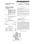
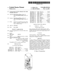
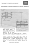
1
6502 SECOND PROCESSOR SERVICE MANUAL
Part no 0408,003
Issue 1
May 1984
Within this publication the term 'BBC' is used as an abbreviation for '
British Broadcasting Corporation'.
ACORN and THE TUBE are trademarks of Acorn Computers Ltd.
Copyright Acorn Computers Limited 1984
Neither the whole or any part of the information contained in, or the product
described in, this manual may be adapted or reproduced in any material form
except with the prior written approval of Acorn Computers Limited (Acorn
Computers).
The product described in this manual and products for use with it, are
subject to continuous development and improvement. All information of a
technical nature and particulars of the product and its use (including the
information and particulars in this manual) are given by Acorn Computers in
good faith. However, it is acknowledged that there may be errors or omissions
in this manual. A list of details of any amendments or revisions to this
manual can be obtained upon request from Acorn Computers Technical Enquiries.
Acorn Computers welcome comments and suggestions relating to the product and
this manual.
All correspondence should be addressed to:Technical Enquiries
Acorn Computers Limited
Newmarket Road
Cambridge
CB5 8PD
All maintenance and service on the product must be carried out by Acorn
Computers' authorised dealers. Acorn Computers can accept no liability
whatsoever for any loss or damage caused by service or maintenance by
unauthorised personnel. This manual is intended only to assist the reader in
the use of this product, and therefore Acorn Computers shall not be liable
for any loss or damage whatsoever arising from the use of any information or
particulars in, or any error or omission in, this manual, or any incorrect
use of the product.
This manual is for the sole use of Acorn Computers' authorised dealers and
must only be used by them in connection with the product described within.
First published 1984
Published by Acorn Computers Limited
6502 SECOND PROCESSOR SERVICE MANUAL
page
Contents
1
Introduction
1
2
Packaging and Installation
2
3
3.1
3.2
3.3
3.4
3.5
3.6
Specification
The 6502 Second Processor
Tube Operating System
BASIC
Power Supply
Environmental
Outside Dimensions
3
3
3
3
3
4
4
4
Disassembly and Assembly
5
5
5.1
5.2
5.3
5.4
5.5
Circuit Description
General
Power-Up
After Power-up
PCB Links
Tube Connector Pinout
6
6
6
6
7
8
6
6.1
6.2
6.3
The Tube
Tube Registers
Tube Pinout
Timing
9
9
12
14
7
7.1
7.2
7.3
7.3.1
7.3.2
7.4
7.4.1
7.4.2
7.4.3
7.5
7.5.1
7.5.2
7.5.3
7.5.4
7.5.5
Fault Finding on the 6502 Second Processor
General
Start-up Message Printed
Total Failure
Power Supply
Oscillator
Checking the Second Processor in Boot Mode
PHI Generation Circuit
Reset and ROM Enable Circuitry
CPU
Checking the Second Processor in Run Mode
PHI Generation Circuit
Refresh Circuitry
DRAMs
CPU
The Tube IC1
15
15
15
15
16
17
17
18
18
18
19
19
19
20
21
21
APPENDIX
IC Number and Function
General Assembly
Block Diagram
Main PCB Circuit Diagram
Assembly Drawing
Power Supply Board Circuit Diagram
Parts List
23
25
27
29
31
33
35
37
WARNING: THE COMPUTER MUST BE EARTHED
IMPORTANT: The wires in the mains lead for the second processor are coloured
in accordance with the following code:
GREEN & YELLOW - EARTH
BLUE - NEUTRAL
BROWN - LIVE
As the colours of the wires may not correspond with the coloured markings
identifying the terminals in your plug, proceed as follows:
The wire which is coloured green and yellow must be connected to the terminal
in the plug which is marked by the letter E, or by the safety earth symbol
, or coloured either green or green and yellow.
The wire which is coloured blue must be connected to the terminal which is
marked by the letter N, or coloured black.
The wire which is coloured brown must be connected to the terminal which is
marked by the letter L, or coloured red.
If the socket outlet available is not suitable for the plug supplied, the plug
should be cut off and the appropriate plug fitted and wired as previously
noted. The moulded plug which was cut off must be disposed of as it would be
a potential shock hazard if it were to be plugged in with the cut off end of
mains cord exposed.
The moulded plug must be used with the fuse and the fuse carrier firmly in
place. The fuse carrier is of the same basic colour* as the coloured insert in
the base of the plug. Different manufacturers' plugs and fuse carriers are
not interchangeable. In the event of loss of the fuse carrier the moulded plug
MUST NOT be used. Either replace the moulded plug with another conventional
plug wired as previously described, or obtain a replacement fuse carrier from
an authorised BBC Microcomputer dealer. In the event of the fuse blowing, it
should be replaced, after clearing any faults, with a 3 amp fuse that is ASTA
approved to BS 1362.
*Not necessarily the same shade of that colour.
1. Introduction
This manual is intended to provide the information required to diagnose and
repair faults on the 6502 second processor (a part of the BBC Microcomputer
system) which was designed by Acorn Computers Ltd of Cambridge, England.
The information contained in this manual is aimed at service engineers and
Acorn dealers who will be servicing the 6502 second processor on behalf of
Acorn Computers Ltd.
2. Packaging and Installation
The 6502 second processor is supplied in a two part moulded
polystyrene packing which is further packaged within a cardboard
sleeve. Supplied with the second processor is a User Guide, a ROM
labelled DNFS, a ROM labelled HIBASIC, and a guarantee card.
The DNFS ROM must be plugged into one of the BBC Microcomputer's
sideways ROM sockets, or the second processor system will not work,
see 3.2.
The socket on the second processor ribbon cable should be plugged into
the connector labelled TUBE under the BBC Microcomputer Keyboard.
A mains power switch is located at the rear of the second processor.
A T315mA fuse is located at the rear of the second processor. Before
tampering with the fuse the second processor must be disconnected from
the mains. Access to the fuse may be gained by undoing the round cover
with the slot in it using a screwdriver. The mains must not be
reconnected until the fuse is relocated correctly in its holder with
the cover screwed shut.
Do not use the second processor in conditions of extreme heat, cold,
humidity or dust or in places subject to vibration. Do not block
ventilation under or behind the second processor. Ensure that no
foreign objects are inserted through any openings in the second
processor.
3. Specification
3.1 The 6502 second processor
A second processor for the BBC Microcomputer operating through THE TUBE
giving faster processing speed, more user memory, faster BASIC. The
second processor is contained in a rigid injection moulded
thermoplastic case and contains the following:
A 3MHz 6502
64K of read/write Random Access Memory
4K Read Only Memory containing part (2 Kbytes) of the Tube Operating
System (TOS)
The Tube - a fast asynchronous communication path connecting the
second processor to the I/O processor (BBC Micro)
3.2 Tube operating system
The Tube operating system is divided between the second processor and
the I/O processor. The 2K of code in the second processor is stored in
a ROM labelled 6502 BR (boot ROM) and on power-up or BREAK is copied to
RAM locations &F800 to &FFFF in the second processor. The 1K of code in
the I/O processor is stored in a ROM labelled DNFS and on power-up or
BREAK is copied to RAM locations &400 to &7FF in the I/O processor. All
the usual BBC Microcomputer OS calls are available on the second
processor.
3.3 BASIC
On power-up, the rightmost language ROM in the I/O processor's sideways
ROM sockets is copied across the Tube into the second processor's
memory. Standard BBC BASIC (ROM identification number PB01 or P1305) is
copied into locations &8000 to &BFFF. HI-BASIC, which is supplied with
the second processor, may be copied into locations &B800 to &F7FF (
allowing more user-RAM space for programs if required).
All of BBC BASIC's facilities are available on the second processor,
and execution speed is up to twice as fast as the BBC Microcomputer
alone.
3.4 Power supply
Max AC input 264V AC
Min ACinput 216V AC
Power rating 14 watts
Supply frequency 47-63 Hz
Max output current 1A at +5V
3.5 Environmental
Minimum
Maximum
Minimum
Maximum
operating temperature
+5 degrees C
operating temperature +35 degrees C
storage temperature
-20 degrees C
storage temperature
+70 degrees C
Maximum operating humidity
Maximum storage humidity
3.6 Outside dimensions
Height
72mm
Width
207mm
Depth
346mm
95% RH at 35 degrees C
95% RH at 55 degrees C
4 Disassembly and assembly
To service the 6502 second processor, disconnect it from the mains and
undo the three fixing screws, two at the top of the back panel and one
underneath nearest the front equidistant between the two rubber feet. (
The assembly diagram is given in the Appendix.) The lid can now be
removed revealing the transformer and power supply board held in place
by six screws, and the main PCB. It is recommended that the transformer
and power supply board are not unscrewed from the case unless
absolutely necessary.
To remove the main PCB from the case, pull off the two "fast on" tabs
which connect the power supply (brown +5V and black OV leads), and
remove the four screws which hold the PCB in place.
5
5 Circuit Description
5.1 General
The microprocessor used in the 6502 second processor is a 6502C with
clock signals provided by a 12MHz crystal oscillator (IC8) in
conjunction with divider circuitry (IC12). The processor runs at 3MHz.
Random Access (Read/Write) Memory is provided by 8 64Kbit DRAMs (ICs 18
to 25), giving 64Kbytes in all. Thus the memory map for the second
processor consists entirely of RAM.
5.2 Power-up
On power-up, the second processor runs for about 0.25 of a second in "
boot mode", and the Tube Operating System code in the second processor
ROM is copied into RAM at locations &F800 to &FFFF. The second
processor is thereafter executing code from RAM only, and the ROM is
not accessed again.
IC26 is a monostable which, on power-up, supplies a logic 0 to IC6 pin
10 and IC2 pin 40 (RST) for approximately 100µs. The D-type flip-flop
contained in IC6, thus set, enables the divide by 16 counter (IC11 pin
9), the ROM chip select (IC3 pin 18), and the read/write ROM/RAM toggle
circuit (NAND gate pins 4 5 and 6 of IC10). When RST goes high the CPU
starts to operate and accesses the ROM.
PHI IN (the processor main clock input) to the second processor is
supplied from IC12 pin 13 (divide by 4). In boot mode this counter (
IC12) is enabled by the divide by 16 counter (IC11) and so the PHI IN
frequency is 3/16MHz = 187.5 kHz.
When R/W is high (read), the NAND gate (pins 4 5 and 6) in IC10 applies
a reset to pin 13 IC9 which disables the CAS input to the DRAMs. When
R/W is low (write) then CAS is enabled. This means that in boot mode,
read operations read from the ROM, and write operations write to the
RAM, thus allowing the code to be copied across.
Boot mode is terminated by the software when it selects any one of the
Tube addresses. The address is decoded by the NAND gate in IC4, which
pulls pin 12 of IC6 low, thereby resetting the output. This deselects
the ROM, and disables IC11 which allows IC12 to generate PHI IN at
3MHz.
5.3 After power-up
The second processor is now running at 3MHz and entirely in RAM. The
NAND gate (pins 4 5 and 6 of IC10) now inhibits the action of the RAM
by supressing CAS only when the Tube chip itself (IC1) is being
accessed, ie when IC4 pin 9 is logic 0.
The whole second processor is halted when the NOR gate (pins 8 9 and 10
of IC14) detects a collision. This happens when both the host (BBC
Microcomputer) and parasite (second processor) select the Tube
simultaneously, by pulling both HCS and PCS low.
6
Timing of the DRAM refresh is handled by counter 1C13, which requests a
refresh by setting pin 55 high (which also pulls pin 7 low to stall the
counter while the refresh is taking place). The NAND gate (pins 8 9 and
50 of 1C50) waits for SYNC to go high signalling the end of an
instruction cycle and pulls the READY line low to stall the processor.
It also pulls 1C57 pin 59 low and 1C55 pin 59 high which deselects the
row address from the CPU and enables the refresh address from 1C7. 1C7
is an 8-bit counter which holds the address of the next row to be
refreshed, and ICs 55 56 and 57 are address buffers. RAS, driven
directly (but inverted) from PHI 1N, goes low to execute the refresh,
and on its rising edge clocks pin 3 of the D-type flip-flop in 1C6,
which clears the refresh request and reloads the timer (IC53). This in
turn increments the refresh address held in 1C7.
For information on the operation of the Tube (IC13) see section 6.
5.4 PCB Links
The second processor PCB has 5 links numbered LK5 to LK5 and a Disable
link. These links are hard-wired in the correct position for normal
use. The action of these links is as follows:
LK2 when made powers the whole second processor from the BBC
Microcomputer's power supply. The second processor power supply leads
must be disconnected before LK5 is made. Running the second processor
from the BBC's power supply may overload it and this practice is not
recommended.
LK2 when made connects the H1RQ line. H1RQ is the interrupt request
line from the second processor to the I/O processor, and is not used by
standard software. If LK2 is made the BBC Microcomputer will not work
when the second processor is powered down.
LK3 controls the source of the power supply to the BBC peripherals in
the Tube chip. In its hard-wired position, LK3 selects power for the
BBC half of the Tube chip from the BBC's power supply. LK3 must not be
altered.
LK4 is included to replace the diode Dl. (Dl and R6 are not fitted
because the disable feature is not implemented). If the Disable link is
made then LK4 must be broken.
LK5 ensures the correct refresh rate for use with a processor running
at 4MHz. At 3MHz it must not be altered.
Disable is not implemented, but may be used if LK4 is broken (see LK4).
7
5.5 Tube connector pinout
The tube connector pinout is as shown below:
TOP
0V
0V
0V
0V
0V
0V
0V
0V
0V
0V
0V
0V
0V
0V
0V
+5V
+5V
+5V
+5V
+5V
Pin No BOTTOM
1
2 R/NW (read/not-write)
3
4 2MHzE
5
6 N1RQ (not-interrupt request)
7
8 NTUBE
9
10 NRST (not-reset)
11 12 D0
13 14 D1
15 16 D2
17 18 D3
19 20 D4
21 22 D5
23 24 D6
25 26 D7
27 28 A0
29 30 Al
31 32 A2
33 34 A3
35 36 A4
37 38 A5
39 40 A6
8
6 The Tube
The Tube (IC1) is a custom chip which provides parallel asynchronous
communication between two processor systems, the BBC Microcomputer (
host) and the second processor (parasite). To each processor system it
resembles a conventional peripheral device, occupying 8 bytes of memory
or I/O space.
Figure 1 Tube concept
6.1 Tube Registers
As can be seen from Figure 1, each system (host or parasite) has access
to 4 read only registers and 4 write only registers. In addition, each
read only register has an associated status register, and the host
system also has access to a single write only status register.
Figure 2 shows the Tube registers in more detail
9
Figure 2 Schematic diagram of Tube registers
10
The following tables show the relative address and type of each
register in the Tube, firstly for the host system, and secondly for the
parasite system.
Table 1 Host system registers
Address Read
000
Status flags and Register 1 flags
001
Register 1 (24 byte F1FO read only)
010
Register 2 flags
011
Register 2 (1 byte read only)
100
Register 3 flags
101
Register 3 (2 byte F1FO read only)
110
Register 4 flags
111
Register 4 (1 byte read only)
Address Write
000
Status flags
001
Register 1 (1
010
011
Register 2 (1
100
101
Register 3 (2
110
111
Register 4 (1
byte write only)
byte write only)
byte F1FO write only)
byte write only)
Table 2 Parasite system registers
Address Read
000
Status flags and Register 1 flags
001
Register 1 (1 byte read only)
010
Register 2 flags
011
Register 2 (1 byte read only)
100
Register 3 flags
101
Register 3 (2 byte F1FO read only)
110
Register 4 flags
111
Register 4 (1 byte read only)
Address Write
000
001
Register
010
011
Register
100
101
Register
110
111
Register
1 (24 byte F1FO write only)
2 (1 byte write only)
3 (2 byte F1FO write only)
4 (1 byte write only)
11
As can be seen from Figure 2 and Tables 1 and 2, each numbered
register (eg register 1) is actually two registers, one for reading
and one for writing. The register selected is determined by R/W on the
host side, and by PNRDS/PNWDS on the parasite side (see 6.2).
Some of the registers are single byte latches, and others are F1FO
buffers which store two or more bytes to be read out in the same order
they were put in. Data is stored in the Tube until removed by the
receiving processor, thus allowing completely asynchronous operation
of the two systems. Messages and data are passed to and fro through
the various registers according to carefully designed software
protocols which allow both systems to operate with the minimum waiting
time.
6.2 Tube Pinout
Figure 3 shows the pinout diagram for the Tube 1C.
Figure 3 Pinout diagram for Tube 1C
12
Description of pins:
Power supply
GND
VCC1
VCC2
VCC3
0V supply rail
Parasite main +5V supply
Parasite secondary supply
Host +5V supply
Data buses
HD0-7
PD0-7
8-bit data bus to host processor
8-bit data bus to parasite processor
Address signals HA0-2
PA0-2
HCS
PCS
Timing signals
HPHI2
HR/W
PNRDS
PNWDS
Interrupt lines HRST
PRST
P1RQ
PNM1
H1RQ
3 register select lines from host
3 register select lines from parasite
Host chip select
Parasite chip select
Host PHI2 - high level signifies valid
address bus
Host read/write line - determines whether
read or write register is selected on
address specified by HA0-2, and direction
data flow on HD0-7
Parasite read strobe (active-low)
Parasite write strobe (active-low)
Host reset (RST) - initialises Tube to
known state and generates PRST
Reset (RST) line to parasite processor
Interrupt to parasite
Non-maskable interrupt to parasite
Interrupt to host (not used by 6502
second processor)
DMA lines
DRQ
Request for DMA transfer
DACK
DMA acknowledge from DMA controller
DMA facility is not used by the 6502 second processor
13
6.3 Timing
Figure 4 gives the Tube timing diagram.
Figure 4 Tube timing diagram
1
2
3
4
5
6
7
8
9
10
11
-
R/W set up to PHI 2 (host PH1 2)
timing strobe pulse width
address set up time
address and chip select hold times
data out delay time
data out hold time
data in set up time
data in hold time
R/W hold time
cycle time
CS set up time
35ns
110ns
35ns
10ns
70ns
10ns
50ns
20ns
10ns
250ns
20ns
maximum
maximum
maximum
maximum
minimum
maximum
maximum
maximum
maximum
maximum
maximum
The timing reference for the host is PH1 2, and R/W gives the
direction of transfer.
For the parasite, both timing and direction are given by PNRDS or PNWDS.
14
7 Fault Finding on the 6502 Second Processor
7.1 General
a) The 6502 second processor PCB has three socketed 1Cs (ICs 1 to 3),
so these chips may easily be replaced if necessary.
b) The second processor circuit is difficult to diagnose area by area
because it contains only one subsystem which terminates, namely the
12MHz oscillator. A check on any other subsystem on the board requires
earlier subsystems to be working, but this same argument also applies
to each of them.
c) The second processor system runs entirely in RAM, except for the
first quarter second when the Tube Operating System ROM contents are
copied across at a reduced clock speed of 187.5kHz. It is useful to
bear this in mind when debugging.
7.2 Start-up message printed
Remember from 3.2 that the Tube Operating System software is copied
from ROM to RAM on power-up or CTRL BREAK. If the start-up message
Acorn TUBE 6502 64K
is printed on the screen then the second processor has completed the
boot phase, and the Tube chip (IC1) is operating.
The fault will lie in the DRAMs, see 7.5.3, or the refresh circuitry,
see 7.5.2.
7.3 Total Failure
The usual result of plugging in a broken 6502 second processor is a
blank screen with just the cursor flashing in the top left corner. Most
faults manifest themselves in this way.
If by any chance the "BBC Microcomputer 32K" message is printed on the
screen, then the host is not recognising the presence of the second
processor. This means that the DNFS ROM has not been plugged into the
BBC, or that there is no power supply to the second processor (see 7.3.
1), or that the ribbon cable connection is faulty, or the Tube (I01)
has failed (see 7.5.5).
Check 1C8 pin 12 with an oscilloscope or frequency counter. If
oscillating at 12MHz then the master clock is running, and therefore
the power supply. Try replacing the Tube (IC1) with a known good one
and see if the second processor now works. If not then carry on with
the diagnosis below.
15
7.3.1 Power supply
Check the T315mA mains fuse which can be accessed via a cover at the
rear of the second processor, see section 2.
Check for any loose, disconnected, or broken leads.
After making sure that the second processor is disconnected from the
mains, check the mains switch at the rear of the unit.
Overload protection of the second processor is provided by a thyristor
(TH1) and a fuse (FS1) on the second processor PCB itself. The fuse
protects against overcurrent, and the thyristor protects against
overvoltage by blowing the fuse. Hence, if the fuse is blown it could
be due to either overvoltage or overcurrent, and there is likely to be
either a short circuit somewhere or the power supply board is faulty (
it is supplying too high a voltage).
Disconnect the two power supply leads, brown and black, from the second
processor PCB and connect a 10 ohm 2.5W resistor between them. Measure
the voltage across the brown lead (+5V) and the black lead (ground)
which should be in the range 4.95 to 5.25V with a maximum of 50mV
noise. If the voltage is out of spec then set it to 5V exactly using
the trimmer which is accessible through a hole in the power supply
board, see Figure 5.
Figure 5 Position of voltage trimmer on PSB.
If the measurements obtained are incorrect then replace the power
supply unit.
16
Now remove the resistor connected across the power supply leads and
test the current drawn by the second processor PCB from the +5V supply.
The board should draw between 800 and 1000mA from the power supply.
If the current is zero then the second processor PCB has gone open
circuit so look at the fuse (FS1) and connectors and tracks.
If the fuse is blown then the fault is a short circuit on the PCB.
If the current is higher than it should be then measure the voltage. If
the voltage is greater than 5.25V then adjust it to 5V using the
trimmer, see Figure 4. If the voltage is in spec then one or more of
the components on the second processor PCB is shorting. Switch off the
power supply and feel which of the components is hot.
The Tube (IC1) is powered both from the BBC Microcomputer and from the
second processor. If either of these supplies fails then the second
processor will not work.
With the second processor switched off (ON/OFF switch down), switch on
the BBC Microcomputer (ON/OFF switch up). Check that there is a
potential of 5V between pin 4 (+ve) and pins 1 and 5 (ground) of 1C1.
If not then check the ribbon cable and connectors.
Now switch off the BBC Microcomputer (ON/OFF switch down) and switch on
the second processor (ON/OFF switch up). Check that there is a
potential of 5V between pins 2 and 3 (+ve) and pins 1 and 5 (ground) of
1C1.
7.3.2 Oscillator
Check with the oscilloscope that a 12MHz clock pulse is generated at
pin 12 of 1C8. If not then check the power supply to 1C8, 5V across pin
14 (+ve) and pin 7 (ground). If the oscillator is not working then it
could be a faulty 74S04 (IC 8), the crystal, or any of the passive
components around them.
7.4 Checking the Second Processor in Boot Mode
On power-up the second processor goes into "boot mode" where the
software is copied from the ROM into RAM. This process lasts for
approximately 0.25 of a second. The second processor can also be forced
into boot mode by causing a reset, ie by pulling RST low (IC2 pin 40).
This is easily accomplished by pressing the BREAK key on the host, so
to test the second processor circuit in boot mode will require frequent
use of the BREAK key.
A quick check that the boot phase of operation has probably completed
succesfully is to test 1C6 pin 9. After releasing BREAK, this pin
should be high for 0.25 of a second and then go low, and remain low. If
this does not happen then either the address bus is shorting (check
A15) or the reset pulse is not reaching the monostable (IC26).
17
7.4.1 PHI generation circuit
In boot mode PH1 is derived from the 12MHz clock by dividers 1C11 and
1C12, see 5.2. 1C11 and 1C12 are disabled by the NOR gate (pins 8 9 and
10 of 1C14) and 1C27 when a collision is detected, so the first thing
to check is that 1C14 pin 10 is logic 0 and 1C27 pin 8 is logic 1. (
Remember, it is the quarter second immediately after release of the
BREAK key in which the second processor is operating in boot mode.) If
these logic levels are incorrect then both host and parasite are
attempting to access the Tube 1C (which should not be accessed by
either processor in boot mode if operating correctly).
Test PH1 1N (IC2 pin 37) with an oscilloscope and check that clock
pulses arrive at a frequency of 187.5kHz for the quarter second after
the BREAK key is released. (After this period the frequency will jump
to 3MHz.) If PH1 is not getting through to 1C2 then follow the track
back to 1C12 pin 13 and test there. 1C12 is clocked from the 12MHz and
PH1 is taken from pin 13 which gives a divide by 4. However, in boot
mode 1C11 is enabled (a divide by 16 counter also clocked from the
12MHz) and this divided by 16 pulse is used to enable 1C12, thereby
giving an overall divide by 64.
7.4.2 Reset and ROM enable circuitry.
Carry out the quick check given in 7.4.
Use an oscilloscope on 1C2 pin 40 and check that there is a logic 0
reset pulse when the BREAK key is pressed and released. On release of
the BREAK key the RST line should go high after approximately 100µs. If
it is stuck low then there is a fault in the monostable (IC26) or
possibly the CPU (IC2).
Check that the ROM is receiving its chip enable signal (IC3 pin 18
should be low for 0.25 of a second after BREAK and then go high).
Use a scope on the ROM output enable (IC3 pin 20) and see that the
data bus (IC2 pins 26 to 33) is not floating (3-state) when OE is low.
7.4.3 CPU
Use an oscillosope on 1C2 pin 7 to look at the SYNC output from the
CPU. Press BREAK and on releasing it see that SYNC pulses slowly for
the 0.25 seconds of boot mode, and that it then starts pulsing faster
when the processor runs at 3MHz. If SYNC stops at any time, either
before or after the transition to 3MHz, then the CPU has stopped.
If SYNC doesn't run at all then look for bad connections, power
supplies, and finally replace the CPU.
If SYNC stops in boot mode then the fault could be that the ROM is not
being selected.
If SYNC stops after the transition then the fault is either in the
DRAMs or the refresh circuitry, see 7.5.2 and 7.5.4.
If the above tests are satisfactory then we can proceed to fault
finding in 3MHz normal running mode.
18
7.5 Checking the Second Processor in Run Mode
After all the software has been copied from ROM to RAM the second
processor executes an instruction which accesses one of the Tube
addresses, see section 6. This address is decoded by 1C4 which
deselects the ROM and prevents counter 1C11 from slowing PHI. Thus PH1
IN jumps to 3MHz and the processor runs entirely in RAM (except when
the Tube is accessed in which case the RAM is disabled by holding CAS
high).
7.5.1 PHI generation circuit
In run mode PH1 is derived from the 12MHz clock by divider 1C12. PH1 is
taken from 1C12 pin 13 which divides the clock by 4 giving a frequency
of 3MHz. 1C12 is disabled by the NOR gate (pins 8 9 and 10 of 1C14) and
1C27 when a collision is detected, so PH1 will stop when this happens.
However, this will not occur very often if the processor is running
correctly.
During a write cycle (R/W=0) PH1 is stretched slightly in its high
state by the action of R/W on 1C12 via 1C9 pin 2 and 1C11. This is for
RAM timing purposes, see figure 6.
Use an oscilloscope or frequency counter on 1C2 pin 37 and check that
the processor is receiving a 3MHz clock pulse. If not then either 1C12
is faulty or there is a broken track.
7.5.2 Refresh circuitry
1C13 is wired as a divide by 11 counter, and is clocked direct from the
12MHz. It is enabled from 1C12 pin 15 which is running at 12/16MHz, so
the refresh request signal from 1C13 pin 15 should have a frequency of
68kHz. Check that this signal is reaching IC7 pin 1 and that 1C7 is
counting.
If there is no signal on 1C13 pin 5 then check that pin 9 or pin 7 is
not held low.
If the refresh request is working correctly then check 1C10 pin 6 which
should be operating at the same frequency, but inverted. Also check
that SYNC is coming from the CPU by testing 1C10 pin 5. If SYNC is
stuck at one logic level then the CPU is not running. Test SYNC as
described in 7.4.3 and see whether it stopped in boot mode or run mode.
The fault is most likely to be in the DRAMs.
Check that 1C17 pin 19 is pulsing low at 68kHz.
19
7.5.3 DRAMs
RAS (pin 4 of each DRAM 1C) is driven through an inverter direct from
PHI, and should therefore be oscillating at a frequency of 3MHz. In
practice, during a write cycle (R/W=0) RAS is stretched slightly by
the action of R/W on the PH1 generation circuit, see 7.5.1. If RAS is
stopped then check PHI, see 7.5.1. Note that if RAS is stuck low then
the DRAMs may be destroyed.
CAS (pin 15 of each DRAM 1C) is driven from 1C9 pin 8, and runs at
3MHz except when the Tube is accessed in which case CAS is disabled,
and during a write cycle when CAS is stretched slightly. On read
cycles CAS is triggered from the processor R/W line (IC2 pin 34) gated
with PH1 2 (IC2 pin 39) via 1C5 and the asynchronous set input 1C9 pin
10. On write cycles CAS is clocked from 1C12 pin 14 (PH1 1N times 2),
and the clock is stretched by the action of R/W on 1C12, see 7.5.1. If
CAS has stopped then check 1C9 pins 10 and 13 which should be high. If
either is stuck low then check whether the processor has stopped by
seeing whether PH1 2 is oscillating (IC2 pin 39). If PH1 2 is stuck
then press BREAK and see at what time this happens. Also check RAS and
CAS after pressing BREAK during boot mode. If the processor stalls
when RAS and CAS are working then there is a fault in selecting the
ROM (see 7.4.2), or one of the DRAM chips is dead.
Figure 6 shows the DRAM timing
Figure 6 DRAM timing
20
7.5.4 CPU
Looking at SYNC (IC2 pin 7) with an oscilloscope will show whether the
CPU keeps running or whether it has stalled (SYNC stuck at one logic
level). If the processor does stall then determine when this happens
after releasing BREAK.
If SYNC does not oscillate at all from the time of releasing BREAK then
look for bad connections, check power supply (7.3.1). After this swap
the CPU itself for a good one.
If SYNC stops in boot mode then check that the ROM is being selected,
see 7.4.2.
If SYNC stops on the transition to 3MHz running or after, then there
is probably a DRAM (7.5.3) or refresh (7.5.2) fault.
7.5.5 The Tube IC1
After checking for short circuits and loose connections check the
power supply to the Tube 1C.
The Tube (IC1) is powered both from the BBC Microcomputer and from the
second processor. If either of these supplies fails then the second
processor will not work.
With the second processor switched off (ON/OFF switch down), switch on
the BBC Microcomputer (ON/OFF switch up). Check that there is a
potential of 5V between pin 4 (+ve) and pins 1 and 5 (ground) of IC1.
If not then check the ribbon cable and connectors.
Now switch off the BBC Microcomputer (ON/OFF switch down) and switch on
the second processor (ON/OFF switch up). Check that there is a
potential of 5V between pins 2 and 3 (+ve) and pins 1 and 5 (ground) of
1C1.
If the power supplies are good then replace the Tube IC with a known
good one.
21
Appendix
23
1C
Number and Function
1C1 Tube 1C - fast asynchronous parallel interface between two
processors
1C2 6502C microprocessor - 4MHz spec 6502
1C3 2732 ROM - contains the Tube Operating System which is copied into
RAM on power-up and reset
1C4 74LS133 - multi-input NAND gate to decode Tube select addresses
1C5 74LS00 - general gating
1C6 74LS74 - one D-type used for boot mode, the other to reset the
refresh timer
1C7 74LS393 - 8-bit counter to provide refresh address
1C8 74S04 - oscillator and general gating
1C9 74LS74 - one D-type to generate CAS, the other to stretch PH1
during a write cycle
1C10 74LS00 - general gating
1C11 74LS161 - boot mode divide by 16
1C12 74LS163 - divide by 4 for PH1 generation
1C13 74LS163 - refresh timer
1C14 74LS02 - general gating
1C15 81LS95 1C16 81LS95 - 3-state address buffers
1C17 81LS95 1C18
1C19
1C20
1C21
1C22
1C23
1C24
1C25
64Kbit
64Kbit
64Kbit
64Kbit
64Kbit
64Kbit
64Kbit
64Kbit
DRAM
DRAM
DRAM
DRAM
DRAM
DRAM
DRAM
DRAM
- 64Kbytes of random access read/write memory
-
1C26 74LS122 - monostable to supply reset pulse on release of BREAK key
1C27 74F74 - D-type used in collision detection circuitry
25
Block diagram
29
Main PCB circuit
diagram
31
35
6502 2ND PROCESSOR PARTS LIST
Item Part no
Description
Qty Notes
1
208,000
BARE PCB
1
2
3
4
520,120
RESISTOR 12 ohm 1W 10%
1 R1
5
502,560
RESISTOR 56ohm 1/4W 5%
2 R2,3
6
502,102
RES1STOR 1K 1/4W 5%
2 R4,5
7
502,391
RESISTOR 390 ohm 1/4W 5%
1 R7
8
628,101
CAPACITOR 100n DISC CERAMIC
1 C30
9
610,010
CAPAC1TOR 10µF 10V TANTALUM
1 C3
10 629,010
CAPACITOR 10nF PLATE CERAMIC
1 Cl
11 631,033
CAPACITOR 33pF PLATE CERAMIC
4 C2,31,32,33
12 680,002
CAPACITOR DECOUPLER
27 C4-28,34
13 637,333
CAPACITOR 33pF MULTILAYER CERAMIC 1 C29
14
15 742,000
INTEGRATED C1RCUIT 74LS00
2 1C5,10
16 742,002
INTEGRATED CIRCUIT 74LS02
1 1C14
17 741,004
1NTEGRATED CIRCU1T 74S04
1 1C8
18 741,074
INTEGRATED CIRCUIT 74S74
2 1C9,27
19 742,074
1NTEGRATED C1RCUIT 74LS74
1 1C6
20 742,133
1NTEGRATED CIRCUIT 74LS133
1 1C4
21 741,161
1NTEGRATED CIRCU1T 74S161
1 1C11
22 742,163
INTEGRATED C1RCU1T 74LS163
2 1C12,13
23 742,393
INTEGRATED CIRCUIT 74LS393
1 1C7
24 742,122
1NTEGRATED C1RCUIT 74LS122
1 1C26
25 738,095
1NTEGRATED CIRCUIT 81LS95
3 1C15-17
26 704,164
1NTEGRATED CIRCUIT 4164-15
8 1C18-25
27 706,503
1NTEGRATED C1RCU1T 6502C
1 1C2
28 201,606
1NTEGRATED CIRCU1T 2732
1 1C3 BOOT ROM
29 201,605
INTEGRATED CIRCUIT TUBE U.L.A.
1 1C1
30
31 820,120
CRYSTAL 12MHz
1 X1
32
33
34 795,006
ZENER DIODE BZY88 5.1V
1 D2
35
36 800,124
I.C. SOCKET DIL 24 WAY
1
37 800,140
I.C. SOCKET DIL 40 WAY
2
38
39 815,010
FUSE 2 AMP 20mm x 5mm
1 FS1
40 791,000
THYRISTOR
1 TH1
41
42
43 800,037
S.H.E. CONNECTOR
1 PL1 (bottom
44
half)
45 800,200
FASTON TAB
2
46
47 815,910
FUSE CL1P P.C.B. 20mm x 5mm
2
48
49
50 882,122
M3 x 8mm LG. PAN HD. SCREW
1
51 882,902
M3 NUT FULL
1
52 882,962
M3 WASHER PLA1N
1
53 882,972
M3 WASHER SHAKEPROOF
1
54
37
6502 2ND PROCESSOR PARTS LIST (cont'd)
Item Part no
Description
Qty Notes
1
2
201,110
CASE LOWER MOULDING
1
3
201,109
CASE UPPER MOULDING
1
4
201 106
CASE LABEL REAR
1
5
201,103
CASE LABEL UPPER
1
6
108,000
6502 PCB ASSEMBLY
1
7
104,001
POWER SUPPLY ASSEMBLY
1
8
201,084
MA1NS CABLE ASSEMBLY
1
9
201,146
RIBBON CABLE ASSEMBLY
1
10 800,024
CABLE GROMMET
1
11
12 815,900
FUSE HOLDER
1
13 815,901
FUSE HOLDER SHROUD
1
14 815,007
FUSE 20mm x 5mm 1 AMP RATING
1
15 805,003
MAINS SWITCH
1
16
17 882,654
SELF TAPPING PAN HD SCREW No 6 x 9.5mm 6 SUPERDRIVE
18 882,652
SELF TAPP1NG PAN HD SCREW No 6 x 6.5mm 5 SUPERDRIVE
19 800,210
1/4" CRIMP CONN. SHROUDED RECEPTACLE
2
20 800,702
SOLDER TAG M4
1
21
22 880,030
CABLE CLIP
2
23 882,946
SPIRE CLIP No 6
2
24 882,665
SELF TAPP1NG PAN HD SCREW No 6 x 13mm
3 SUPERDRIVE
25 870,111
W1RE 16/0.2 BROWN
1 CUT TO 70mm
26 890,000
BUMP-ON FEET
4
27
28 008,000/PG PACKAG1NG ASSEMBLY
29
30 800,037
S.H.E. CONNECTOR
1 TOP HALF
38