1
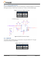
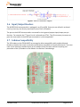
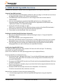
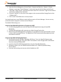
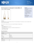
Figure 3. Power Supply Schematic
Table 2. FRDM-KL02Z Power Supplies
Power Supply Name
P5-9V_VIN
P5V0_USBER
P3V3_VREG
P3V3_BATT
P3V3
P3V3_MCU
P3V3_USBER
Description
Power supplied from the VIN pin of the I/O headers (J9 pin 8).
8
Power supplied from the OpenSDA USB connector (J2 and J9(pin
J9( 5)).
A Schottky diode provides back drive protection.
Regulated 3.3V supply
supply.. Sources power to the P3V3 supply rail
through a back drive protection Schottky diode. 1
Coin cell battery supply voltage. Sources power to the P3V3 supply
rail through a back drive protection Schottky diode.
Main supply rail for the FRDM-KL02Z assembly.. May be sourced from
P3V3_VREG, P3V3_BATT, or directl
directlyy from the I/O headers (J9 pin 2
and pin 44)
KL02Z MCU supply. Header J4 provides a convenient means for
energy consumption measurements. 2
OpenSDA circuit supply. Header J5 provides a convenient means for
energy consumption measurements. 2
Notes:
1) By default the linear regulator, U6
U6,, is a 3.3V output regulator. However, this
is a common footprint that would allow the user to modify the assembly to
utilize an alternative device such as a 1.8V or 2.5V regulator. The KL02Z
microcontroller has an operating range of 1.71V to 3.6V.
2) J4 and J5 are not populated by default. The two pins of these headers are
shorted together by a trace on the bottom layer of the PCB. To measure the
energy consumption of either the KL02Z or the OpenSDA MCU, the trace
between these pins
ns must first be cut. A current probe or a shunt resistor and
voltage meter can then be applied to measure the energy consumption on these
rails.
FRDMKL02ZUM
FRDM-KL02Z User Manual
Page 6 of 11