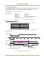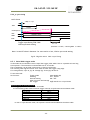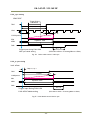
1
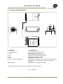
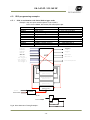
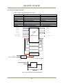
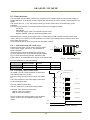
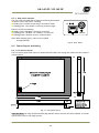
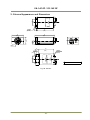
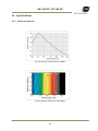
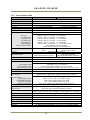
User's Manual CM-140GE CB-140GE Digital Monochrome / Color Progressive Scan GigE Vision Camera Document Version: 1.0 Camera Revision: 0 CM-140 GE / CB-140 GE Table of Contents 1. General ............................................................................................................ - 4 2. Camera nomenclature ........................................................................................... - 4 3. Main Features ..................................................................................................... - 5 4. Locations and Functions......................................................................................... - 6 5. Pin Assignment ................................................................................................... - 7 5.1. 12-pin Multi-connector (DC-in/GPIO/Iris Video) ..................................................... - 7 5.2. Digital Output Connector for Gigabit Ethernet....................................................... - 7 6. GPIO (General purpose inputs and outputs)................................................................. - 8 6.1. Overview................................................................................................... - 8 6.1.1. LUT (Look Up Table) .............................................................................. - 8 6.1.2. 12-bit Counter ..................................................................................... - 9 6.1.3. Pulse Generators .................................................................................. - 9 6.2. Opto-isolated Inputs/Outputs .......................................................................... - 9 6.2.1 Recommended External Input circuit diagram for customer ............................... - 9 6.2.2 Recommended External Output circuit diagram for customer ............................ - 10 6.2.3 Optical Interface Specifications ................................................................ - 10 6.3. Inputs and outputs table ............................................................................. - 11 6.4. Configuring the GPIO module (register settings) ................................................... - 11 6.4.1. Input/Output Signal Selector................................................................... - 11 6.4.2. 12bit counter ..................................................................................... - 12 6.4.3. Pulse generators (20 bit x 4) ................................................................... - 12 6.5. GPIO programming examples.......................................................................... - 14 6.5.1 GPIO in combination with Pulse Width trigger mode ...................................... - 14 6.5.2 Internal Trigger Generator ....................................................................... - 15 7. GigE Vision Streaming Protocol (GVSP) ..................................................................... - 16 7.1. Digital Video Output (Bit Allocation)................................................................. - 16 7.2. Bit Allocation (Pixel Format / Pixel Type) – CM-140GE (monochrome) ......................... - 16 7.2.1. GVSP_PIX_MONO8 (8bit) ........................................................................ - 16 7.2.2. GVSP_PIX_MONO10 (10bit) ..................................................................... - 16 7.2.3. GVSP_PIX_MONO10_PACKED ( 10 bit ) ........................................................ - 17 7.3. Bit Allocation (Pixel Format / Pixel Type) – CB-140GE (Bayer mosaic color) .................. - 17 7.3.3 GVSP_PIX_BAYRG8 “ BayerRG8 “ ............................................................... - 17 7.3.4 GVSP_PIX_BAYRG10 “Bayer RG10” .............................................................. - 17 7.3.1 GVSP_PIX_BAYGB8 “BayerGB8” .................................................................. - 17 7.3.2 GVSP_PIX_BAYGB10 “BayerGB10” ............................................................... - 18 8. Functions and Operations ...................................................................................... - 19 8.1. GigE Vision Standard Interface......................................................................... - 19 8.2. Recommended Network Configurations .............................................................. - 19 8.2.1 Verified Network Interface Cards (NICs) ....................................................... - 19 8.2.2 Video data rate (network bandwidth) .......................................................... - 20 8.2.3 How to set Jumbo Frame (in WindowsTM environments) ................................... - 20 8.2.4 Packet delay ...................................................................................... - 22 8.3. Basic functions ........................................................................................... - 23 8.3.1 Vertical Binning (CM-140GE only). ........................................................... - 23 8.3.2 CB-140GE. Bayer mosaic filter .................................................................. - 23 8.3.3 Electronic Shutter................................................................................. - 24 8.3.4. Auto Iris Lens video output (12-pin Hirose connector) ..................................... - 25 8.3.5 Auto-detect LVAL-sync / a-sync. accumulation .............................................. - 25 8.3.6 Rear panel indicator. ............................................................................ - 26 8.4. Sensor Layout and timing .............................................................................. - 26 8.4.1. CCD Sensor Layout ................................................................................ - 26 8.4.2. Horizontal timing ................................................................................. - 27 8.4.3. Vertical timing..................................................................................... - 27 8.4.4. Partial Scanning ................................................................................... - 28 Vertical Timing ............................................................................................ - 28 - -2- CM-140 GE / CB-140 GE 8.4.5. Vertical binning ................................................................................... - 29 8.5. Operation Modes ......................................................................................... - 30 8.5.1 Continuous operation ............................................................................ - 30 8.5.2 Pre-Select trigger mode ......................................................................... - 31 LVAL_sync timing.......................................................................................... - 31 LVAL_a-sync timing ....................................................................................... - 32 8.5.3 Pulse Width trigger mode ....................................................................... - 32 LVAL_sync timing.......................................................................................... - 33 LVAL_a-sync timing ....................................................................................... - 33 8.5.4 Sequential Trigger Mode (Pre-Select trigger) ............................................... - 34 8.5.5 Delayed Readout mode (Pre-Select trigger) ................................................. - 35 8.5.6 Optical Black transfer mode..................................................................... - 36 8.6. Operation Mode and Functions matrix ............................................................... - 37 9. Register Map ..................................................................................................... - 37 9. External Appearance and Dimensions........................................................................ - 47 10. Specifications .............................................................................................. - 48 10.1. Spectral response ...................................................................................... - 48 10.2. Specification table..................................................................................... - 49 11. Appendix ........................................................................................................ - 51 Precautions ..................................................................................................... - 51 Typical Sensor Characteristics ............................................................................... - 51 References ...................................................................................................... - 51 11. User's Record............................................................................................... - 54 - -3- CM-140 GE / CB-140 GE 1. General This manual covers the digital monochrome progressive scan camera CM-140GE and color progressive scan camera CB-140GE The CM-140GE/CB-140GE is a GigE Vision compliant camera, based on the CM-140MCL/CB140MCL. Both the monochrome version CM-140GE and the color version CB-140GE provide a frame rate of 31 frames/second at full resolution in continuous operation. Using vertical binning (CM-140GE only) and partial scan provides higher frame rates. The 1/2" CCD with square pixels offers a superb image quality. The high-speed shutter function and asynchronous random trigger mode allows the camera to capture high quality images of fast moving objects. The color version CB-140GE, based on CCD sensor with primary RGB Bayer mosaic filter, outputs raw Bayer images. Host-based color interpolation is required to display or save color images. The CM-140GE/CB-140GE also complies with the GenICam standards, as it has in internal XML file that is used to describe the functions/features of the camera. For further information on GenICam please go to www.emva.org. As an application programming interface, JAI provides an SDK (Software Development Kit). This SDK includes software documentation, register information, code examples and objects such as Transport Layer and Device Drivers (High Performance Filter Driver and Standard Windows Stack). The JAI SDK can be downloaded from www.jai.com The latest version of this manual can be downloaded from www.jai.com For camera revision history, please contact your local JAI distributor. 2. Camera nomenclature The standard camera composition consists of the camera main body and C-mount protection cap. The camera is available in the following versions: CM-140 GE Where C stands for "Compact" family, M stands for "Monochrome", 140 represents the resolution "1.4 million pixel" and GE stands for "GigE Vision" interface CB-140 GE Where C stands for "Compact" family, B stands for "Bayer mosaic color", 140 represents the resolution "1.4 million pixel" and GE stands for "GigE Vision" interface -4- CM-140 GE / CB-140 GE 3. Main Features • • • • • • • • • • • • • • • Member of C3 Compact series, covering VGA to UXGA resolution 1380 (h) x 1040 (v) 4.65 µm square pixels 1/2” progressive scan – Monochrome and Bayer mosaic color versions 31 frames/second with full resolution in continuous operation 30 frames/second with external trigger and full resolution Increased frame rate with vertical binning (CM-140 GE only) and partial scan Exposure time from 30.584μs to 2 sec. using Pulse Width trigger mode Programmable exposure from 61.168μs to 32.17 ms in Full Frame scan Sequencer trigger mode for on-the –fly change of gain, exposure and ROI Pre-select and Pulse Width trigger modes LVAL-synchronous/-asynchronous operation (auto-detect) Auto iris lens video output allows a wider range of light GigE Vision Interface with 10 or 8-bit output Programmable GPIO with opto-isolated inputs and outputs Comprehensive software tools and SDK for Windows XP/Vista -5- CM-140 GE / CB-140 GE FCC seal 4. Locations and Functions ④ ⑧ ③ GigE ⑨ POWER/ TRIG ② 1 2 3 4 Lens mount CCD sensor 12-pin connector RJ-45 5 h i j LED LED LED Holes for RJ-45 thumbscrews 9Mounting holes ⑥ ⑤ Serial No. ⑦ Caution seal ① C-mount (Note *1) 1/2 inch CCD sensor DC +12V power and GPIO interface Gigabit Ethernet connector with treaded holes for thumbscrews Indication for power and trigger input GigE Network condition : LINK GigE Network condition : ACT When an RJ-45 connector with thumbscrews is used, remove the two screws located above and below the Ethernet connector. M3 depth 4mm for tripod mount plate *1) Note: Rear protrusion on C-mount lens must be less than 10.0mm. Fig. 1. Locations -6- CM-140 GE / CB-140 GE 5. Pin Assignment 5.1. 12-pin Multi-connector (DC-in/GPIO/Iris Video) Type: HR10A-10R-12PB (Hirose) male. (Seen from rear of camera.) 9 1 2 4 8 10 11 3 Pin no. Signal Remarks 1 GND 2 +12 V DC input 3 Opto IN 2 (-) / GND (*1) 4 Opto IN 2 (+)/Iris Video out (*1) 5 Opto IN 1 ( - ) 6 Opto IN 1 ( + ) GPIO IN / OUT 7 Opto Out 1 ( - ) 8 Opto Out 1 ( + ) 9 Opto Out 2 ( - ) 10 Opto Out 2 ( + ) 11 + 12 V DC input 12 GND *1 : Iris Video output function can be set by the internal DIP switch. 7 12 5 6 Fig. 2. 12-pin connector. 5.2. Digital Output Connector for Gigabit Ethernet Type: RJ-45 HFJ11-1G02E-L21RL or equivalent The CM-140GE and CB-140GE cameras also accept industrial RJ-45 connectors with thumbscrews. This assures that the connector does not come undone in tough industrial environments. Please contact the nearest JAI distributor for details on recommended industrial RJ-45 connectors. Fig. 3. Gigabit Ethernet connector The digital output signals follow the Gigabit Ethernet interface using RJ-45 conforming connector. The following is pin assignment for Gigabit Ethernet connector. Pin No 1 2 3 4 5 6 7 8 In/Out In/Out In/Out In/Out In/Out In/Out In/Out In/Out In/Out Name MX1+ (DA+) MX1- (DA-) MX2+ (DB+) MX3+ (DC+) MX3- (DC-) MX2- (DB-) MX4+ (DD+) MX4- (DD-) -7- CM-140 GE / CB-140 GE 6. GPIO (General purpose inputs and outputs) 6.1. Overview All input and output signals pass through the GPIO (General Purpose Input and Output) module. The GPIO module consists of a Look-Up Table (LUT – Cross-Point Switch), 4 Pulse Generators and a 12-bit counter. In the LUT, the relationship between inputs, counters and outputs is governed by internal register set-up. LVAL IN DVAL IN FVAL IN EEN IN OPT IN 1 OPT IN 2 Soft Trigger Soft Trigger Soft Trigger Soft Trigger TRIGGER 0 TRIGGER 1 LUT 0 1 2 3 OPT OUT 1 OPT OUT 2 Time Stamp Reset (Cross point switch) Pulse Generator 3 ( 20 bit Counter ) Pulse Generator ( 20 bit Counter ) Pulse Generator ( 20 bit Counter ) Pulse Generator ( 20 bit Counter ) 25MHz Pixel Clock 12 bit Counter The blocks shown in the above diagram have the following functionality: 6.1.1. LUT (Look Up Table) The LUT works as a cross-point switch which allows connecting inputs and outputs freely. The signals LVAL_IN, DVAL_IN, FVAL_IN and EEN_IN all originate from the camera timing circuit. Trigger 0 is connected to the camera's timing circuit and is used for initiating triggered exposure. Trigger 1 is used for Delayed Readout mode. The Time Stamp Reset signal is used reset the camera's time stamp function, also making it possible to reset and synchronize the time stamp of multiple cameras. -8- CM-140 GE / CB-140 GE 6.1.2. 12-bit Counter A 25MHz clock or the camera pixel clock (65MHz) can be used as a source. The counter has a “Divide by N”, where N has the range 1 through 4096, allowing a wide range of clock frequencies to be programmed. 6.1.3. Pulse Generators (0 to 3) Each pulse generator consists of a 20-bit counter. The behavior of these signals is defined by their pulse width, start point, end point and number of repetitions. The pulse generator signals can be set in either triggered or periodic mode. In triggered mode, the pulse is triggered by the rising edge/falling edge/high level or low level of the input signal. In periodic mode, the trigger continuously generates a signal that is based on the configured pulse width, starting point and end point. 6.2. Opto-isolated Inputs/Outputs The control interface of the C3 GigE Vision camera series has opto-isolated inputs and outputs, providing galvanic separation between the camera's inputs/outputs and peripheral equipment. In addition to galvanic separation, the opto-isolated inputs and outputs can cope with a wide range of voltages; the voltage range for inputs is +3.3V to +24V DC whereas outputs will handle +5V to +24V DC. The below figure shows the functional principle (opto-coupler) of the opto-isolated inputs/outputs. Fig.4. Opto-coupler 6.2.1 Recommended External Input circuit diagram for customer EXTERNAL INPUT User side Camera Inside hirose-12 c onnector Pin 4 and 6 2k2 Us er Power +3.3V to +24V 10kB 1 2 3 To camera circuit hirose-12 c onnector Pin 3 and 5 2 3 82 Fig.5 To +3.3V External Input Circuit, OPT IN 1 and 2 -9- CM-140 GE / CB-140 GE 6.2.2 Recommended External Output circuit diagram for customer EXTERNAL OUTPUT User side Camera Inside hirose-12 connector Pin 8 and 10 User Power +5V to +24V To +12V 2 From Camera Circuit OUT 270 hirose-12 connector Pin 7 and 9 220 Fig.6. External Output Circuit, OPT OUT 1 and 2 6.2.3 Optical Interface Specifications The relation of the Input signal and the output signal through optical interface is as follows. Time Delay Rise Rise Time Time Delay Fall Fall Time TDR (us) RT (us) TDF (us) FT (us) User Power(VCC) 5V 12V 0.54 0.62 1.2 2.0 1.5 2.4 3.4 4.5 3.3V 0.54 1.2 1.5 3.6 Fig.7. Optical Interface Performance - 10 - 24V 0.68 3.0 2.1 6.8 CM-140 GE / CB-140 GE 6.3. Inputs and outputs table Input Port Output Port Time Stamp Reset OPT OUT1 OPT OUT2 × × × × ○ ○ ○ ○ × × × × × ○ ○ ○ ○ FVAL IN × × × × × ○ ○ ○ ○ EEN IN × × ○ ○ × ○ ○ ○ ○ OPT IN 1 ○ ○ ○ ○ ○ ○ ○ ○ ○ OPT IN 2 ○ ○ ○ ○ ○ ○ ○ ○ ○ Soft Trigger 0 ○ ○ ○ ○ ○ ○ ○ ○ ○ Soft Trigger 1 ○ ○ ○ ○ ○ ○ ○ ○ ○ Soft Trigger 2 ○ ○ ○ ○ ○ ○ ○ ○ ○ Soft Trigger 3 ○ ○ ○ ○ ○ ○ ○ ○ ○ Pulse Gen. 0 ○ ○ ○ ○ ○ × ○ ○ ○ Pulse Gen. 1 ○ ○ ○ ○ ○ ○ × ○ ○ Pulse Gen. 2 ○ ○ ○ ○ ○ ○ ○ × ○ ○ ○ × Trigger 0 Trigger 1 LVAL IN × DVAL IN Pulse Gen. 0 ○ ○ ○ ○ ○ ○ LEGEND: O = valid combination / X = Not valid (do not use this combination) Pulse Gen. 3 Pulse Gen. 1 Pulse Gen. 2 Pulse Gen. 3 6.4. Configuring the GPIO module (register settings) 6.4.1. Input/Output Signal Selector Address Internal Name Selector CAMERA TRIGGER 0xB060 0 (for Camera Trigger) Selector CAMERA Trigger 1 0xB064 (For Delayed Trigger) Selector GPIO PORT 1 0xB070 (Optical Out 1) Selector GPIO PORT 2 0xB074 (Optical Out 2) 0xB090 Pulse Generator 0 Selector 0xB094 Pulse Generator 1 Selector 0xB098 Pulse Generator 2 Selector 0xB09C Pulse Generator 3 Selector 0xB0A0 Selector Time Stamp Reset GenIcam Name Camera Trigger 0 Camera Trigger 1 GPIO_Port1 GPIO_Port2 PulseGenerator0 PulseGenerator1 PulseGenerator2 PulseGenerator3 TimeStampReset - 11 - Access Size R/W 4 R/W 4 R/W 4 R/W 4 R/W 4 R/W 4 R/W 4 R/W 4 R/W 4 Value (Range) GPIO Selector: 0x00:CAMERA LVAL IN 0x01:CAMERA DVAL IN 0x02:CAMERA FVAL IN 0x03:CAMERA EEN IN 0x04:GPIO Port 1 IN 0x05:GPIO Port 2 IN 0x0C:SOFT TRIG 0 0x0D:SOFT TRIG 1 0x0E:SOFT TRIG 2 0x0F:SOFT TRIG 3 0x10:Pulse Generator 0 0x11: Pulse Generator 1 0x12: Pulse Generator 2 0x13: Pulse Generator 13 0x7F:No Connect Add 0x80 will result in active low output. CM-140 GE / CB-140 GE 6.4.2. 12bit counter Address Internal Name 0xB000 Counter Clock Choice GenIcam Name ClockSource Access Size R/W 4 R/W 4 ClockPreScaler 0xB004 Counter Dividing Value Value (Range) 0x00: 25MHz 0x01: Pixel Clock 0x000: Bypass 0x001: 1/2 Dividing 0x002: 1/3 Dividing | 0xFFF: 1/4096 Dividing 6.4.3. Pulse generators (20 bit x 4) There are 4 pulse generators (designated 0 through 3) that can be used to create various timing scenarios by programming start point, endpoint, length and repeats. Start Point End Point Length Address 0xB008 0xB00C Internal Name Length Counter 0 Start point Counter 0(1) 0xB010 GenIcam name Access R/W R/W Size 4 4 Start point Counter 0(2) R/W 4 0xB014 End point Counter 0 R/W 4 0xB018 Counter Clear 0 R/W 4 0xB01C 0xB020 Length Counter 1 Start point Counter 1(1) R/W R/W 4 4 0xB024 Start point Counter 1(2) R/W 4 0xB028 End point Counter 1 R/W 4 0xB02C Counter 1 Clear R/W 4 0xB030 0xB034 0xB038 Length Counter 2 Start point Counter 2(1) Start point Counter 2(2) R/W R/W R/W 4 4 4 - 12 - Value (range) 0x00001 to 0xFFFFF 0x00000 to 0xFFFFF 0x00: infinite 0x01: 1 time | 0xFF: 255 times 0x00001 to 0xFFFFF 0x00: Free Run 0x01: High Level Clear 0x02: Low Level Clear 0x04: Rising Edge Clear 0x08: Falling Edge Clear 0x00001 to 0xFFFFF 0x00000 to 0xFFFFF 0: Infinite 1: 1 time | 255: 255 times 0x00001 to 0xFFFFF 0x00: Free Run 0x01: High Level Clear 0x02: Low Level Clear 0x04: Rising Edge Clear 0x08: Falling Edge Clear 0x00001 to 0xFFFFF 0x00000 to 0xFFFFF 0x00: Infinite CM-140 GE / CB-140 GE 0xB03C Address End point Counter 2 Internal Name R/W Access 4 Size 0xB040 Counter 2 Clear R/W 4 0xB044 0xB048 Length Counter 3 Start point Counter 3(1) R/W R/W 4 4 0xB04C Start point Counter 3(2) R/W 4 0xB050 End point Counter 3 R/W 4 0xB054 Counter 3 Clear R/W 4 GenIcam name - 13 - 0x01: 1 time | 0xFF: 255 times 0x00001 to 0xFFFFF Value (range) 0x00: Free Run 0x01: High Level Clear 0x02: Low Level Clear 0x04: Rising Edge Clear 0x08: Falling Edge Clear 0x00001 to 0xFFFFF 0x00000 to 0xFFFFF 0x00: Infinite 0x01: 1 time | 0xFF: 255 times 0x00001 to 0xFFFFF 0x00: Free Run 0x01: High Level Clear 0x02: Low Level Clear 0x04: Rising Edge Clear 0x08: Falling Edge Clear CM-140 GE / CB-140 GE 6.5. GPIO programming examples 6.5.1 GPIO in combination with Pulse Width trigger mode Example: 10µs unit pulse width exposure control (PWC). Pixel clock is 65MHz. 650 clocks (750-100) equals 10µs. Address 0xA040 0xB000 0xB004 0xB008 0xB00C 0xB010 0xB014 0xB018 0xB060 0xB090 Register Trigger Mode Clock Choice Counter Dividing Value Length Counter 0 Start point Counter 0 Repeat Count 0 End point Counter 0 Counter Clear 0 CAMERA TRIGGER Selector Pulse Generator 0 Selector Value 2 = Pulse Width 1 = Pixel Clock (65 MHz) 0 = Pass through 1000 Clocks 100 Clocks 1 750 Clocks 4 = Rising Edge Clear 11 = pulse generator 0 4 =OPT IN 1 LVAL IN DVAL IN FVAL IN EEN IN Trigger 0 Trigger 1 LUT OPT IN 1 OPT IN 2 Soft Trigger 0 Soft Trigger 1 Soft Trigger 2 Soft Trigger 3 OPT OUT 1 OPT OUT 2 (Cross point switch) Time Stamp Reset ( Cross Point Switch ) Pulse Generator 3 (20bit Counter) Pulse Generator 2 (20bit Counter) Pulse Generator 1 (20bit Counter) Pulse Generator 0 (20bit Counter) 25 MHz Pixel Clock 12bit 12bit Counter Counte OPT IN 1 Pulse Generator 0 output 100 750 Fig.8. Pulse Generator Timing Example 1 1000 - 14 - CM-140 GE / CB-140 GE 6.5.2 Internal Trigger Generator Create a trigger signal and trigger the camera Register Trigger Mode Clock Choice Counter Dividing Value Length Counter 0 Start point Counter 0 Repeat Count 0 End point Counter 0 Counter Clear 0 CAMERA TRIGGER Selector Address 0xA040 0xB000 0xB004 0xB008 0xB00C 0xB010 0xB014 0xB018 0xB058 Value 1 = Pre-Select (PS) 1 = Pixel Clock 1987 = 1/1988 dev(Line Rate) 1000 Clocks 100 Clocks 0 = Free Run 500 Clocks 0 = No Clear 11 = pulse generator 0 LVAL IN DVAL IN FVAL IN EEN IN Trigger 0 Trigger 1 LUT OPT IN 1 OPT IN 2 Soft Trigger 0 Soft Trigger 1 Soft Trigger 2 Soft Trigger 3 (Cross point switch) ( Cross Point Switch ) Pulse Generator 3 (20bit Counter) Pulse Generator 2 (20bit Counter) Pulse Generator 1 (20bit Counter) Pulse Generator 0 (20bit Counter) 25 MHz Pixel Clock(65MHz) 12bit 12bit Counter Counte Li ne Rat e 32. 696KHz Pulse Generator 0 output 100 Line 500 Line 1000 Line Fig.9. Pulse Generator 0 timing Example 2 - 15 - OPT OUT 1 OPT OUT 2 Time Stamp Reset CM-140 GE / CB-140 GE 7. GigE Vision Streaming Protocol (GVSP) 7.1. Digital Video Output (Bit Allocation) Although the CM-140GE and CB-140GE are digital cameras, the image is generated by an analog component, the CCD sensor. The table and diagram below show the relationship between the analog CCD output level and the digital output. CCD out Black 200mV 230mV Analog Signal * Setup 3.6%, 25mV 700mV 800mV Digital Out(10-bit) 32LSB 890LSB 1023LSB The standard setting for 10-bit video level is 890 LSB. 200 mV CCD output level equals 100% video output. 1023 Wh i te C l ip Leve l 890 D ig i ta l Ou t [LSB ] 100 % Leve l B lack Leve l 32 0 25 Ana log S igna l m [ V] 700 800 Fig. 10. Digital Output 7.2. Bit Allocation (Pixel Format / Pixel Type) – CM-140GE (monochrome) In the GigE Vision Interface, GVSP (GigE Vision Streaming Protocol) is used as an application layer protocol relying on the UDP transport layer protocol. It allows an application to receive image data, image information and other information from a device. In the monochrome camera, CM-140GE, the following pixel types supported by GVSP are available. With regard to the details of GVSP, please refer GigE Vision Specification available from AIA (www.machinevisiononline.org). 7.2.1. GVSP_PIX_MONO8 (8bit) 1Byte 2Byte 3Byte Y0 Y1 Y2 0 1 2 3 4 5 6 7 0 1 2 3 4 5 6 7 0 1 2 3 4 5 6 7 7.2.2. GVSP_PIX_MONO10 (10bit) 1Byte 2Byte 3Byte 4Byte Y0 Y0 Y1 Y1 0 1 2 3 4 5 6 7 8 9 X X X X X X 0 1 2 3 4 5 6 7 8 9 X X X X X X - 16 - CM-140 GE / CB-140 GE 7.2.3. GVSP_PIX_MONO10_PACKED ( 10 bit ) Y0 Y1 Y2 Y3 2 3 4 5 6 7 8 9 0 1 X X 0 1 X X 2 3 4 5 6 7 8 9 2 3 4 5 6 7 8 9 0 1 X X 0 1 X X 2 3 4 5 6 7 8 9 Address 0xA410 Internal Name Access Size R/W 4 Pixel Format type Value 0x01080001:Mono8 0x01100003:Mono10 0x010C0004:Mono10 Packed 7.3. Bit Allocation (Pixel Format / Pixel Type) – CB-140GE (Bayer mosaic color) In the Bayer mosaic color camera, CB-140GE, the following pixel types supported by GVSP (GigE Vision Streaming Protocol) are available. With regard to the details of the GVSP, please refer GigE Vision Specification available from AIA (www.machinevisiononline.org). 7.3.3 GVSP_PIX_BAYRG8 “ BayerRG8 “ Odd Line 1 Byte 2 Byte 3 Byte R0 G1 R2 0 1 2 3 4 5 6 7 0 1 2 3 4 5 6 7 0 1 2 3 4 5 6 7 Even Line G0 B1 G2 0 1 2 3 4 5 6 7 0 1 2 3 4 5 6 7 0 1 2 3 4 5 6 7 7.3.4 GVSP_PIX_BAYRG10 “Bayer RG10” Odd Line 1 Byte 2 Byte 3 Byte 4 Byte R0 R0 G1 G1 0 1 2 3 4 5 6 7 8 9 X X X X X X 0 1 2 3 4 5 6 7 8 9 X X X X X X Even Line G0 G0 B1 B1 0 1 2 3 4 5 6 7 8 9 X X X X X X 0 1 2 3 4 5 6 7 8 9 X X X X X X 7.3.1 GVSP_PIX_BAYGB8 “BayerGB8” Odd Line G0 B1 G2 0 1 2 3 4 5 6 7 0 1 2 3 4 5 6 7 0 1 2 3 4 5 6 7 Even Line R0 G1 R2 0 1 2 3 4 5 6 7 0 1 2 3 4 5 6 7 0 1 2 3 4 5 6 7 - 17 - CM-140 GE / CB-140 GE 7.3.2 GVSP_PIX_BAYGB10 “BayerGB10” Odd Line 1 Byte 2 Byte 3 Byte 4 Byte G0 G0 B1 B1 0 1 2 3 4 5 6 7 8 9 X X X X X X 0 1 2 3 4 5 6 7 8 9 X X X X X X Even Line R0 R0 G1 G1 0 1 2 3 4 5 6 7 8 9 X X X X X X 0 1 2 3 4 5 6 7 8 9 X X X X X X Address 0xA410 Note: Internal Name Pixel Format type Access Size R/W 4 Value 0x01080009:BAYRG8 0x0108000A: BAYGB8 0x0110000D:BAYRG10 0x0110000E:BAYGB10 CB-140GE has the same Bayer sequence for Full and any of partial scanning as RG. Therefore, comparing full scanning and partial scanning, the centre might be shifted. As the Pixel Format type, CB-140GE supports BAYER GB 8 and BAYER GB 10. When this type is selected, the output starts from 2nd line for all scanning. - 18 - CM-140 GE / CB-140 GE 8. Functions and Operations 8.1. GigE Vision Standard Interface The CM-140GE and CB-140GE are designed in accordance with the GigE Vision standard. In transmits digital images over Cat5e or Cat6 Ethernet cables. All camera functions are also controlled via the GigE Vision interface. The camera can operate in continuous mode, providing an endless stream of images. For capturing individual images, related to a specific event, the camera can also be trigged. For precise triggering, it is recommended to use a hardware trigger applied to the Hirose 12-pin connector. It is also possible to initiate a software trigger through the GigE Vision interface. However, when using software trigger, certain latency inherent to the GigE interface must be anticipated. This latency, that manifests itself as jitter, greatly depends on the general conditions and traffic on the GigE connection. The frame rate described in this manual is for the ideal case and may deteriorate depending on conditions. When using multiple cameras (going through a switch and/or a single path) or when operating in a system with limited transmission bandwidth the Delayed Readout Mode and Inter-Packet Delay functions can be useful. 8.2. Recommended Network Configurations Although the CM-140GE and CB-140GE conform to Gigabit Ethernet (IEEE 802.3) not all combinations of network interface cards (NICs) and Switches/Routers are suitable for use with the GigE Vision compliant camera. JAI will endeavor to continuously verify these combinations, in order to give users the widest choice of GigE components for their system design. 8.2.1 Verified Network Interface Cards (NICs) At the time of publishing this document these combinations have been verified: NIC manufacturer Intel Intel Intel Model PRO/1000MT (PWLA8490MT) PRO/1000GT (PWLA8391GT) PRO/1000PT (EXPI9300PT) PCI Bus PCI-X Bus PCI-Express Bus √ (33MHz) √(100MHz) − √ (33MHz) √ (33MHz) − − − √ ( x1 ) Minimum PC requirements are as follows in order to fulfill the above conditions: Intel Core 2 Duo , 2.4GHz or better, alternatively AMD Athlon 64 x2, CPU At least 2 GB memory Video Card with PCI Express Bus x 16 , VRAM better than DDR2 with 256 MB or more, and display capability of 2560 x 1600 More than 200 GB free disk space Windows XP, SP2 (32bit) Do not use screen saver and power save functions. Pentium 4 type PC is not recommended due to dependency on chip set bus performance. - 19 - CM-140 GE / CB-140 GE 8.2.2 Video data rate (network bandwidth) The video bit rate for CM-140GE and CB-140GE is: Model Pixel Type CM-140GE CB-140GE MONO8 MONO10_PACKED MONO10 BAYRG8,BAYGB8 BAYRG10,BAYBG10 Packet data volume (In case the Packet size is 1500) 372Mbit/s 559Mbit/s 745Mbit/s 372Mbit/s 745Mbit/s In case using Jumbo Frame, the packet data will be improved 2 %. For CM-140GE and CB-140GE, the jumbo frame can be set at maximum 4040 Bytes (Factory setting for packet size is 1428 Byte). To set Jumbo Frame, refer chapter 8.2.3. To ensure the integrity of packets transmitted from the camera is recommended to follow these simple guidelines: 1. Whenever possible use a peer-to-peer network. 2. When connecting several cameras, going though a network switch, make sure it is capable of handling jumbo packets and that it has sufficient memory capacity. 3. Configure inter-packet delay to avoid congestion in networks switches. 4. Disable screen saver and power save functions on computers. 5. Use high performance computers with multi-CPU, hyper-thread and 64-bit CPU, etc. 6. Only used Gigabit Ethernet equipment and components together with the camera. 7. Use at least Cat5e or preferably Cat6 Ethernet cables. 8. Whenever possible, limit the camera output to 8-bit. 8.2.3 How to set Jumbo Frame (in WindowsTM environments) (1) Click [start] and click [Control Panel]. (2)Click [Performance and Maintenance]. (3)Click [System]. (4)Click [Hardware] tab. (5)Click [Device Manager]. - 20 - CM-140 GE / CB-140 GE (6)Expand [Network adapters]. (7) Select target NIC, right-click, and click [Properties]. Note: The following procedure is the case you use Intel(R)1000. Accordingly the procedure is different if you use different NIC appeared on Network Adaptors. In that case, set the item of a similar content described here.. (8)Click [Advanced] tab. - 21 - CM-140 GE / CB-140 GE (9) Select Jumbo Frames of Property, and select 9014 of Value. (10)Click [OK]. (11)Close [Device Manager]. (12)Close [System Properties] clicking [OK]. 8.2.4 Packet delay When using multiple cameras (going through a switch and/or a single path) or when operating in a system with limited transmission bandwidth, the Delayed Readout Mode and Inter-Packet Delay functions can be useful. Packet Delay (interval between each packet) Packet Packet This is set in the camera control tool. - 22 - CM-140 GE / CB-140 GE 8.3. Basic functions The CM-140GE and CB-140GE cameras are progressive scan cameras with 10 or 8-bit video output in Gigabit Ethernet. An analogue iris video signal (DIP switch select) can be used for controlling auto-iris lenses. The camera has 1/2, 1/4 or 1/8 partial scanning for faster frame rates. Vertical binning is also available. The camera can operate in continuous mode as well as in 4 triggered modes: - Pre-Select - Pulse Width - Sequential trigger (with pre-selected exposure time) - Delayed readout (with pre-selected exposure time) Depending on the timing of the trigger input in relationship to FVAL (camera internal Frame Valid clock), the start of exposure can be immediate (no-delay, LVAL asynchronous) or delayed until next LVAL (LVAL synchronous). In the following section these functions are described in detail. 8.3.1 Vertical Binning (CM-140GE only). No V binning The binning functions can be used to achieve higher frame rate or higher sensitivity. The drawback is V binning lower resolution. Vertical binning is done by adding the charge from pixels in adjacent lines in the horizontal CCD register. Fig. 11 shows the binning principle. Resolution and frame rate for all combinations are shown in the below table. The CM-140GE has 2:1 Vertical Binning: Setting Value for Register Resolution address 0xA084 (pixels) Off (no binning) 0x01 1380(h) x 1040(v) 2:1 binning 0x02 1380(h) x 520(v) 8.3.2 CB-140GE. Bayer mosaic filter CB-140GE is a color camera based on a CCD sensor with a Bayer RGB color mosaic. The color image reconstruction is done in the host PC. The Color sequence in the video signal is the same for all scanning formats. H Xsg1 Video out Fig.11. CM-140GE binning. Frame rate 31.08 fps. 48.86 fps. FVAL Timing Line # from FVAL triming Actual V Line # 1 1 R G R G B G Full 62 173 R G R G B G 2/3 Partial 91 261 R B G G R G R B R G G 1/2 Partial 134 391 R G R G B G 1/4 Partial 156 455 R G R G B G 1/8 Partial 7 The line readout follows LVAL. The first valid pixel is the same timing as DVAL. The Bayer color sequence starts with: GBG for even line numbers. RGR for odd line numbers. Figure 12 shows the timing sequence for the Bayer mosaic read-out for the available partial scan modes. LVAL 1 DVAL Fig.12. Bayer layout for each scanning - 23 - CM-140 GE / CB-140 GE 8.3.3 Electronic Shutter CM-140GE / CB-140GE have conventional shutter functions as well as the GenICam standard “Exposure Time Abs” function. Preset Shutter 10 steps preset shutter are available: OFF (1/31); 1/60, 1/100; 1/250; 1/500; 1/1,000; 1/2,000; 1/4,000; 1/8,000; 1/10,000 sec. (See the register map included in the SDK documentation for details how to configure this register - 0xA004) Programmable Shutter It is possible to set the shutter speed in the range of 2L to 1052L by 1L unit, in case of Full Frame operation. When 625L is set, it is the equivalent of “OFF (1/31)“ or 32.17ms. (See the register map included in the SDK documentation for details how to configure this register - 0xA008) Normal V Binning Minimum Shutter Time 2L 30.584µs(1L) * 2 = 61.168µs 38.83µs * 2L = 77.66µs Maximum Shutter Time 30.584µs * 1052L≈ 1 Frame(32.17ms) 38.83µs * 527L ≈ 20.46ms Pulse Width Control With this mode selected the exposure time is controlled by the width of the trigger pulse. The minimum trigger pulse width is equal to 1L (30.584µs) Exposure Time Abs (GenICam Standard) This is a function specified in the GenICam standard. The shutter speed can be entered as an absolute exposure time in microseconds (μs) in register address 0xA018. The entered absolute time (Time Abs) is then converted to programmable exposure (PE) value inside the camera. The below equations show the relationship between the PE value used by the camera for the different readout modes and the "Exposure Time Abs" value entered in register 0xA018. As the calculation is based on rounding down to the closest integer, precise values may not always occur. The relation between PE value and Time Abs: Normal readout PE= 2 + INT ( Exposure time -61) µs / (1988 [pixel clocks/line]/65000000[pixel clk]) V Binning readout PE= 2 + INT ( Exposure time -77) µs / (2524/65000000) INT means integer (rounded down). The below table shows minimum and maximum values for each readout mode. Normal Scan Minimum value 61µs Maximum Value 32,175 ms 2/3 Partial Scan 61µs 25,019 ms 1/2 Partial Scan 61µs 21,471 ms 1/4 Partial Scan 61µs 16,149 ms 1/8 Partial Scan 61µs 13,519 ms V-Binning Scan 77µs 20,464 ms GPIO in combination with Pulse Width trigger More precise exposure time can be obtained by using the GPIO in combination with Pulse Width trigger mode. The clock generator and counter can be programmed in very fine increments. - 24 - CM-140 GE / CB-140 GE As for the setting example, refer to chapter 6.5.1. 8.3.4. Auto Iris Lens video output (12-pin Hirose connector) This analogue signal is not routed through the GPIO. This signal is available at pin 4 of 12-pin Hirose connector. It can be used for lens iris control in Continuous mode only. The signal is taken from the CCD sensor output before the gain circuit. The video output is without sync. The signal is 0.7 Vpp from <400 Ω AC coupled. Video Output 75 10k GND Fig. 13. Video output circuit. To use this signal, an internal DIP switch must be set as follows: The auto-iris lens video output is enabled by setting switch SW600 to ON (to the left). The internal DIP switch is set to OFF (to the right) as factory default. Fig. 14. Iris video output. 8.3.5 Auto-detect LVAL-sync / a-sync. accumulation This function replaces the manual setting found in older JAI cameras. Whether accumulation is synchronous or a-synchronous in relationship to LVAL depends on the timing of the trigger input. When trigger is received while FVAL is high (during readout), the camera works in LVAL-synchronous mode, preventing reset feed trough in the video signal. There is a maximum jitter of one LVAL period from issuing a trigger and accumulation start. When trigger is received when FVAL is low, the cameras works in LVAL-asynchronous mode (no delay) mode. This applies to both pre-select (PS) trigger mode and pulse width trigger (PW) mode. Ext. trigger (1) (2) (3) FVAL (1) In this period camera executes trigger at next LVAL (prevents feed-through noise) (2) Avoid trigger at FVAL transition (+/- 1 LVAL period), as the function may randomly switch between "next LVAL" and "immediate". (3) In this period camera executes trigger immediately (no delay) Fig. 15. Auto-detect LVAL sync /a-sync accumulation - 25 - CM-140 GE / CB-140 GE 8.3.6 Rear panel indicator. The rear panel mounted LED provides the following information: Amber: Power connected - initiating Steady green: Camera is operating in Continuous mode Flashing green. The camera is receiving external trigger Ethernet Connector indicates, Steady Green: 1000 Base-T has been connected Flashing green: 100 Base-T or 10 Base-T is connected Flashing amber: Network active in communication Note: When flashing green, video Is not streamed through Ethernet. GigE POWER/ TRIG Fig.16. Rear Panel 8.4. Sensor Layout and timing 8.4.1. CCD Sensor Layout The CCD sensor layout with respect to pixels and lines used in the timing and video full frame read out is shown below. Fig. 17. CCD sensor layout Important Note: By using the Optical Black (OB) transfer mode, the user can select whether to include optical black pixels in the image stream. - 26 - CM-140 GE / CB-140 GE 8.4.2. Horizontal timing The LVAL period is shown for normal continuous mode. 1 LVAL 1988clk=30.584us 1clk=15.38ns LVAL DATA OUT Valid data 1392ck OB 40ck 1432ck DVAL 556ck 1392ck 16ck Fig. 18. Horizontal timing 8.4.3. Vertical timing The FVAL period for normal continuous mode full scan is shown. FULL FRAME READ OUT FRAME RATE 1052L 31.08fps LVAL FVAL 123 3L 7L 1038 1039 1040 1040L 2L Valid data OB DAVL DATA OB CCDExposure EEN XEEN Fig. 19. Vertical timing for full scan - 27 - OB CM-140 GE / CB-140 GE 8.4.4. Partial Scanning The FVAL period is shown for 1/2 partial scan in normal continuous mode. 1 line = 26.7 μs Vertical Timing The below diagram and table provide vertical timing information for the fixed partial scan settings 1/2, 1/4, 1/3 and 2/3 PATIAL FRAME READ OUT LVAL FVAL DAVL 3L DATA Valid data CCD Exposure EEN XEEN A B C Values for vertical timing in partial scan continuous mode. AREA FVAL Low (L) A (L) 1/2 3 91 1/4 3 134 1/8 3 156 2/3 3 62 B (L) Start line End line 520 261 780 260 391 650 130 455 584 694L 173 866 C (L) Total line (L) frame rate (fps) 88L 702L 46.57 131L 528L 61.92 153L 442L 73.97 59L 818L 39.97 Fig. 20. Vertical timing for partial scanning - 28 - CM-140 GE / CB-140 GE Horizontal Timing The horizontal timing is the same the full scanning. 1 LVAL 1988clk=30.584us 1clk=15.38ns LVAL DATA OUT Valid data 1392ck OB 40ck 1432ck DVAL 556ck 1392ck 16ck Fig.21. Horizontal Timing for Partial Scanning 8.4.5. Vertical binning Vertical binning combines charge from two adjacent lines, reducing the vertical resolution to half and at the same time increasing frame rate and sensitivity. By activating this function, the frame rate is increased to 48.87 fps. This function is available only for CM-140GE. Important Note Vertical Binning can not be used together with the Partial Scanning. Horizontal Timing Vertical Binning 1LVAL 2524ck=38.83us 1ck=15.38us LVAL DATA OUT Valid data OB 1392ck 40ck 1432ck DVAL 1392ck Fig.22. Horizontal Timing for Vertical Binning - 29 - 1092ck 16ck CM-140 GE / CB-140 GE Vertical timing Vertical Binning FRAME RATE 527L 48.86fps LVAL FVAL 1+2 3+4 1037+1038 1039+1040 DAVL 3L DATA 3L 520L OB 1L Valid data OB OB CCD Exposure EEN XEEN Fig.23. Vertical Timing for Vertical Binning 8.5. Operation Modes This camera can operate in 5 primary modes. 1. 2. 3. 4. 5. Continuous mode Pre-Select trigger mode Pulse Width trigger mode Sequential trigger Delayed Readout trigger Pre-selected exposure. Pre-selected exposure. Pulse width controlled exposure. Pre-selected exposure Pre-selected exposure 8.5.1 Continuous operation For applications not requiring asynchronous external trigger, but where a continuous stream of images is required, this mode should be used. In this mode it possible to use a lens with video controlled iris. For timing details, refer to fig. 18. through fig. 23. To use this mode: Set function: Trigger mode Scanning Vertical binning Shutter mode Shutter speed Programmable exposure - 30 - Continuous Full, Partial scanning On/Off (CM-140GE only) Preset, Programmable, Auto CM-140 GE / CB-140 GE 8.5.2 Pre-Select trigger mode An external trigger pulse initiates the capture, and the exposure time (accumulation time) is the fixed shutter speed set by registers. The accumulation can be LVAL synchronous or LVAL a-synchronous. The resulting video signal will start to be read out after the selected shutter time. For timing details, refer to fig. 18. through fig. 25. To use this mode: Set function: Input: Trigger mode Scanning Vertical binning Shutter mode Exposure time Other functions and settings Pre-Select (PS) Full, Partial ON / OFF Preset, Programmable, Abs Shutter speed, Programmable exposure Ext. trigger. GigE interface or 12-pin Hirose Important notes on using this mode Trigger pulse >1 LVAL to <1 FVAL) The following table shows minimum trigger interval in synchronous accumulation mode Full scan 1055 L 1/2 Partial 821 L 2/3 partial 705 L 1/4 Partial 531 L 1/8 Partial 445 L 1/2 V Binning 530 L In case of a-synchronous mode, the exposure time should be added to the above table. LVAL_sync timing LAVL SYNC TRIG 2L (min) LVAL 1L(max) CCD Exposure EEN XEEN Exposure Time FVAL 2L Trigger Input during FVAL HIGH (Full:63us V binning:89us) LVAL sync Mode setting Fig. 24. Edge Pre-select LVAL sync Timing - 31 - CM-140 GE / CB-140 GE LVAL_a-sync timing LAVL ASYNC 7.83μ s± 1μ s TRIG 1L(min) CCD Exposure EEN Exposure Time XEEN FAVL Trigger Input During FVAL LOW 2L ~3L LVAL async Mode setting (Full:63us t o 94us, V binning:89us t o 126us) Note: In case PE value is between 2 or more and 4 or less, LVAL a-sync mode setting Fig.25. Edge Pre-select LVAL a-sync Timing 8.5.3 Pulse Width trigger mode In this mode the accumulation time is equal the trigger pulse width. Here it is possible to have long time exposure. The maximum recommended time is <2 seconds. The accumulation can be LVAL synchronous or LVAL a-synchronous. The resulting video signal will start to be read out after the trigger rising edge. For timing details, refer to fig. 18. through fig. 23 and fig. 26 and 27. To use this mode: Set function: Input: Trigger mode Scanning Vertical binning Other functions and settings Ext. trigger. Pulse Width (PS) Full , Partial ON / OFF GigE interface or 12-pin Hirose Important notes on using this mode Trigger pulse width >1 LVAL to <2 seconds The following table shows minimum trigger interval in synchronous accumulation mode Full scan 1055 L 1/2 Partial 821 L 2/3 Partial 705 L 1/4 Partial 531 L 1/8 Partial 445 L V Binning 530 L In case of a-synchronous mode, the exposure time should be added to the above table. - 32 - CM-140 GE / CB-140 GE LVAL_sync timing LVAL SYNC Trigger Rising Prohibited TRIG 1L(min) LVAL CCD Exposure 1L 1L(max) EEN Exposure Time XEEN FAVL 2L ~ 3L Trigger Input during FVAL HIGH (Full:63us to 94us / V binning:89us to 126us) LVAL sync Mode setting Fig. 26. Pulse width control. LVAL sync. LVAL_a-sync timing LAVL ASYNC 7.83μ s± 1μ s TRIG 1L(min) 1L CCDExposure EEN XEEN Exposure Time FAVL 2L ~3L Trigger Input During FVAL LOW (Full:63us to 94us / V binning:89us to 126us) LVAL ASYNC Mode setting Fig.27. Pulse Width control LVAL a-sync - 33 - CM-140 GE / CB-140 GE 8.5.4 Sequential Trigger Mode (Pre-Select trigger) The ROI, Shutter and Gain values can be preset up to 10 sequences. Along with every trigger input, the image data with the preset sequence is output as described below. Trigger Sequence Operation Sequence 1 Sequence 2 Sequence 3 Sequence 4 Signals added to trigger can be selected by 0xB060 Camera Trigger Selector on register map via GPIO. The camera will functions on the rising edge of the trigger and Negative or Positive should be determined accordingly. For the sequence, the following default settings are installed. ID 1 2 3 4 5 6 7 8 9 10 Width 1392 1392 1392 1392 1392 1392 1392 1392 1392 1392 ROI Offset Height X 1040 0 1040 0 1040 0 1040 0 1040 0 1040 0 1040 0 1040 0 1040 0 1040 0 Offset Y 0 0 0 0 0 0 0 0 0 0 Shutter Gain 1052 1052 1052 1052 1052 1052 1052 1052 1052 1052 0 0 0 0 0 0 0 0 0 0 The following registers are used to configure the sequence. 0xC0F4 0xC0F8 0xA30C 0xB060 0xA040 Sequence Repetitions (Number of Repetitions) Sequence Ending Position (Ending Position) Sequence Reset Command (1 only) Selection for Camera Trigger 0 Trigger mode selection and 0x09 for Sequential PS mode Example of settings Setting : Repeat 5 times from ID 1 through ID 8 0xC0F4 0xC0F8 0xB060 0xA040 0xA3F0 0xA040 Set to 0x05 Set to 0x08 For instance, Pin 6 of the 12-pin Hirose connector for Opto IN 1 Sequential PS(9). Set this for start Set Normal Mode(0) for stop Please refer the detailed register description on Camera Register Map which is included in the SDK. - 34 - CM-140 GE / CB-140 GE The following table shows the minimum trigger interval in a-synchronous accumulation mode. In the sequential mode, only a-synchronous mode is functional. Therefore, the trigger timing should be set so that the timing is not in synchronous mode. Full Scan 1/2 Partial 2/3 Partial 1/4 Partial 1/8 Partial 1/2 V Binning 1052 L 818 L 702 L 528 L 442 L 527 L The conditions for this table is that shutter speed should be set the same for all sequences. If the shutter speed is different, the difference of exposure time should be added. It is recommended to set the exposure time in order of the shortest to the longest one. The minimum interval is > Exposure time (expressed in L[Line]) + FVAL + 2. Here, FVAL is 1052L. For proper operation, It is not allowed to issue a trigger pulse immediately after the sequence is reset. The trigger must be issued at least 500ms after the end of the sequence. 8.5.5 Delayed Readout mode (Pre-Select trigger) This mode can be used to delay the transmission of a captured image. When several cameras are triggered simultaneously and connected to the same GigE interface, it allows the cameras to be read out in sequence, preventing congestion. The image data is not transmitted directly by the trigger 0 and it is stored in the memory located at Ethernet Interface. By the falling edge of the trigger 1, the image data is output. Example of setting 0xA040 0xB060 0xB064 Delayed Readout (0x11) Trigger 0 select, e.g. 0x04 OPT IN 1 Trigger 1 select, e.g. 0x05 OPT IN 2 For the details of Registers, please refer Camera Register Map which is included in the SDK. - 35 - CM-140 GE / CB-140 GE 8.5.6 Optical Black transfer mode It is possible for the user to decide whether the optical black (OB) portion of the image will be transferred or not. The optical black part can be used for black reference in the application software. Setting register 0xA41C turns the optical black transfer ON or OFF. The default condition is OFF. OB Transfer Mode OFF Normal Scan 1 1 OB Transfer Mode ON 1392 1 1 1040 1392 1408 16 pixels for Horizontal, & 4 lines for Vertical are added. 1044 2/3 Partial Scan 1 1 1392 1 1 1392 1408 ます 694 694 1/2 Partial Scan 1 1 1392 1 1 520 1/4 Partial Scan 1 1 16 pixels for Horizontal are added 1392 1408 16 pixels for horizontal are added. 520 1392 1 1 1392 1408 ます 260 260 16 pixels for horizontal are added. 1/8 Partial Scan 1 1 1392 1 1 130 V Binning Scan 1 1 1392 1408 16 pixels for horizontal is added. 130 1392 1 1 1392 1408 ます 520 520 - 36 - 16 pixels for horizontal is added. CM-140 GE / CB-140 GE 8.6. Operation Mode and Functions matrix ID (Value) Note 1 Mode 0x02 0x09 0x11 Vertical Binning Note 2 Partial Scanning LVAL Sync/Async Yes Yes Yes --- Yes Note 3 Yes Yes Auto No Yes Yes Yes Yes Auto Only a-sync No Yes Yes Auto No Continuous 0x00 0x01 Shutter Preset / Program. Pre-Select Yes (PS) Pulse Width Not applicable (PW) Sequential PreSelect Yes (PS) Pre-Select Delayed Yes Readout Auto Iris output Auto No Note 1: Write ID in register address 0xA040 in order to set trigger mode. Note 2: Vertical Binning is available for only CM-140GE. Note 3: Auto iris output is available only on Continuous mode with full resolution or with vertical binning. It cannot be used with partial scan mode. 9. Register Map The below table provides detailed information for the hardware registers used for controlling the camera and obtaining information on the status of the camera. The content of this register map is also found in the XML file, as stipulated by the GenICam standard. Address Function Read / Write Size Generic Registers: 0x0000 Version R 4 0x0004 Device mode R 4 R 4 R 4 0x0008 0x000c Device MAC address (high) Device MAC address (low) Value / Range of value (Major, Minor) vector 0x0010 IP R 4 Bit 0: persistent Bit 1: DHCP Bit 2: LLA 0x0014 IP address setup R/W 4 Bit 0: persistent Bit 1: DHCP Bit 2: LLA 0x0024 0x0034 Current IP address Current subnet mask Current default gateway R R 4 4 R 4 0x0044 - 37 - Description Version of the GigE Standard to which the device is compliant. Information about device mode of operation. Upper 4 bytes of the MAC address Lower 4 bytes of the MAC address Bits can be OR-ed. All other bits are reserved and set to 0. DHCP and LLA bits must be on. Bits can be OR-ed. LLA is always activated and is read only. Default value CM-140 GE / CB-140 GE Function Read / Write Size Value / Range of value Address 0x0048 Manufacturer's name R 32 e.g. JAI 0x0068 Model name R 32 e.g. CM-140GE 0x0088 Device version R 32 0x00A8 Manufacturer specific info R 80 0x00D8 Serial number R 16 0x00E8 Camera ID R/W 16 User assignable string 0x0200 First choice of URL for XML R 51 2 File extension .XML indicates uncompressed text file. File extension .ZIP indicates compressed using ZIP. Description Provides extended manufacturer information about the device. Camera serial number 0x0400 Second choice of URL for XML R 51 2 0x0600 Number of network interfaces R 4 Indicates the number of physical network interfaces on this device. 0x064C persistent IP address R/W 4 Valid if Persistent IP is enabled 0x065C persistent subnet mask R/W 4 Valid if Persistent IP is enabled 0x066C persistent gateway R/W 4 Valid if Persistent IP is enabled 0x0900 number of messaging channels R 4 This camera has 1 0x0904 number of stream channels R 4 This camera only has 1 0x0934 GVCP capability R 4 Bit 31:multiple read Bit 30:WRITEMEM Bit29: ACKETRESEND Bit 28:EVENT Bit 27: EVENTDATA 0x0938 Heartbeat timeout R/W 4 The min. value is 500 ms 0x093C Timestamp tick frequency (High) R 4 Timestamp tick frequency is 0 if timestamp is not supported. 0x0940 Timestamp tick frequency (Low) R 4 0x0944 Timestamp control W 4 Default value number of available message channel number of available stream channel This is a capability register indicating which one of the non-mandatory GVCP commands are supported by this device. In milliseconds. Internally, the heartbeat is rounded according to the clock used for heartbeat. 64-bit value indicating the number of timestamp clock ticks in 1 second. This register holds the most significant bytes. This register holds the least significant bytes. Bit 0: Reset Bit 1:latch current timestamp - 38 - Used to latch the current timestamp value. No need to clear to 0. 0 Address Function Read / Write Size CM-140 GE / CB-140 GE 0x0948 Timestamp (High) R 4 0x094C Timestamp (Low) R 4 0x0a00 CCP R 4 0x0b00 MCP R/W 4 0x0b10 MCDA R/W 4 0x0b14 MCTT R/W 4 0x0b18 MCRC R/W 4 0x0d00 SCP0 RW 4 0x0d04 SCPS0 R/W 4 0x0d08 SCPD0 R/W 4 0x0d18 SCDA0 R/W 4 Value / Range of value Description Default value Latched value of the timestamp (most significant bytes) Latched value of the timestamp (least significant bytes) 0:Disconnect 1:Exclusive 2:Control 3:Exclusive Control Not specified control channel privilege register 0 message channel port register 0 message channel destination address register message channel transfer timeout: ms message channel retry count Not specified Decided by system 32us Max With 62.5MHz Tick Time Not specified Decided by application - 39 - 300 2 primary stream port register primary stream channel packet size register packet size includes IP, UDP&GVSP Header 1440 XML file primary stream channel packet delay register 0 primary stream channel destination address register CM-140 GE / CB-140 GE Function Size Address Read / Write Standard camera functions registers: 0xA000 Shutter mode R/W 4 0xA004 Preset shutter R/W 4 0xA008 Programmable exposure, PE 0xA018 Exposure TimeAbs ( single) R/W R/W 4 4 0xA040 Trigger Mode R/W 4 0xA080 Partial Scan R/W 4 0xA084 Vertical Binning R/W 4 0xA0C4 Manual Gain Level R/W 4 0xA0E0 User Black level R/W 4 0xA13C Test Stream (Jumbo Packet Check) R/W 4 Value / Range of value 0= Preset shutter 1= Programmable exposure 4=Exposure TimeAbs 0=Off; 1=1/60; 2=1/100; 3=1/250; 4=1/500; 5=1/1000; 6=1/2000; 7=1/4000; 8=1/8000; 9=1/10000; Description Sets exposure time for image capture. Fixed values for setting exposure 2 to 1052(OFF) Flexible setting of exposure time ranging from 61.2 µs to 32.2 ms using the LVAL period (L) as increment. 1L is 30.584us. 61 to 32174 (OFF) Actual exposure time in microseconds, µs. The camera will round value off to match LVAL increments. 0x00=Continuous 0x01=Edge preselect 0x02=Pulse width control 0x09=Sequential PS 0x11=Delayed PS 0=Full Frame 1=2/3 Partial 2=1/2 Partial 3=1/4 Partial 4=1/8 Partial 1=Binning OFF 2=1/2 V Binning -84 to 336 0 to 1023 64 LSB=1023 32LSB=512 to 528 CM-140GE 0=OFF 1=White Noise 4=H Ramp Scale 5=V Ramp Scale 6=Moving Ramp Scale - 40 - Default value 0 0 1052 32174 0 0 1 0 525 0 Function Size Address Read / Write CM-140 GE / CB-140 GE 0xA13C Test Stream (Jumbo Packet Check) R/W 4 0xA300 Save Settings into User area W 4 0xA304 Load Settings W 4 0xA308 EPROM current Area No. R 4 0xA30C Save Sequence W 4 Value / Range of value Description CB-140GE 0=OFF 1= White Noise 4=H Ramp Scale 5=V Ramp Scale 6=Moving Ramp Scale 8=Color Bar 9=Color Bar 10=Moving Color Bar 1=User area1 2=User area2 3=User area3 0=Factory area 1=User area1 2=User area2 3=User area3 Default value 0 Allows use to save all camera settings. Last used area number becomes new default. 1 Allow the user to recall all camera settings. 0 0 0 to 3 1 1 only Read / Write Size Sequence function registers: Sequence Shutter 1 R/W 4 2 to 1052 Pre-program 1st shutter value 1052 Sequence Shutter 2 R/W 4 2 to 1052 Pre-program 2nd shutter value 1052 Sequence Shutter 3 R/W 4 2 to 1052 Pre-program 3rd shutter value 1052 Sequence Shutter 4 R/W 4 2 to 1052 Pre-program 4th shutter value 1052 Sequence Shutter 5 R/W 4 2 to 1052 Pre-program 5th shutter value 1052 Sequence Shutter 6 R/W 4 2 to 1052 Pre-program 6th shutter value 1052 Sequence Shutter 7 R/W 4 2 to 1052 Pre-program 7th shutter value 1052 Sequence Shutter 8 R/W 4 2 to 1052 Pre-program 8th shutter value 1052 Sequence Shutter 9 R/W 4 2 to 1052 Pre-program 9th shutter value 1052 Sequence Shutter 10 R/W 4 2 to 1052 Pre-program 10th shutter value 1052 0xC078 Sequence Gain 1 R/W 4 -84 to 326 Pre-program 1st Gain value 0 0xC07C Sequence Gain 2 R/W 4 -84 to 326 Pre-program 2nd Gain value 0 Address 0xC000 0xC004 0xC008 0xC00C 0xC010 0xC014 0xC018 0xC01C 0xC020 0xC024 Function Value / Range of value Description Default value - 41 - Address Function Read / Write Size CM-140 GE / CB-140 GE Value / Range of value Description Default value 0xC080 Sequence Gain 3 R/W 4 -84 to 326 Pre-program 3rd Gain value 0 0xC084 Sequence Gain 4 R/W 4 -84 to 326 Pre-program 4th Gain value 0 0xC088 Sequence Gain 5 R/W 4 -84 to 326 Pre-program 5th Gain value 0 0xC08C Sequence Gain 6 R/W 4 -84 to 326 Pre-program 6th Gain value 0 0xC090 Sequence Gain 7 R/W 4 -84 to 326 Pre-program 7th Gain value 0 0xC094 Sequence Gain 8 R/W 4 -84 to 326 Pre-program 8th Gain value 0 0xC098 Sequence Gain 9 R/W 4 -84 to 326 Pre-program 9th Gain value 0 0xC09C Sequence Gain 10 R/W 4 -84 to 326 Pre-program 10th Gain value 0 0xC0F0 Sequence Reset W 4 1 only 0xC0F4 Sequence Mode Function 1 R/W 4 0xC0F8 Sequence Mode Function 2 R/W 0xC0FC Sequence ROI size- X1 0xC100 Sequence Reset 1 0 to 255 Number of repetition 0 4 0 to 10 Ending position 1 R/W 4 8 to 1392 Width max Sequence ROI Size- X2 R/W 4 8 to 1392 Width max 0xC104 Sequence ROI Size- X3 R/W 4 8 to 1392 Width max 0xC108 Sequence ROI Size- X 4 R/W 4 8 to 1392 Width max 0xC10C Sequence ROI size- X5 R/W 4 8 to 1392 Width max 0xC110 Sequence ROI Size- X 6 R/W 4 8 to 1392 Width max 0xC114 Sequence ROI size- X7 R/W 4 8 to 1392 Width max 0xC118 Sequence ROI Size- X8 R/W 4 8 to 1392 Width max 0xC11C Sequence ROI size- X9 R/W 4 8 to 1392 Width max 0xC120 Sequence ROI Size- X10 R/W 4 8 to 1392 Width max 0xC124 Sequence ROI Size-Y1 R/W 4 8 to 1040 Height Max 0xC128 Sequence ROI Size-Y2 R/W 4 8 to 1040 Height Max 0xC12C Sequence ROI Size-Y3 R/W 4 8 to 1040 Height Max 0xC130 Sequence ROI Size-Y4 R/W 4 8 to 1040 Height Max - 42 - Address Function Read / Write Size CM-140 GE / CB-140 GE Value / Range of value Description Default value 0xC134 Sequence ROI Size-Y5 R/W 4 8 to 1040 Height Max 0xC138 Sequence ROI Size-Y6 R/W 4 8 to 1040 Height Max 0xC13C Sequence ROI Size-Y7 R/W 4 8 to 1040 Height Max 0xC140 Sequence ROI Size-Y8 R/W 4 8 to 1040 Height Max 0xC144 Sequence ROI Size-Y9 R/W 4 8 to 1040 Height Max 0xC148 Sequence ROI Size-Y10 R/W 4 8 to 1040 Height Max 0xC14C Sequence ROI Offset-X1 R/W 4 0 to 1384 0 0xC150 Sequence ROI Offset-X2 R/W 4 0 to 1384 0 0xC154 Sequence ROI Offset-X3 R/W 4 0 to 1384 0 0XC158 Sequence ROI Offset-X4 R/W 4 0 to 1384 0 0xC15C Sequence ROI Offset-X5 R/W 4 0 to 1384 0 0xC160 Sequence ROI Offset-X6 R/W 4 0 to 1384 0 0xC164 Sequence ROI Offset-X7 R/W 4 0 to 1384 0 0xC168 Sequence ROI Offset-X8 R/W 4 0 to 1384 0 0xC16C Sequence ROI Offset-X9 R/W 4 0 to 1384 0 0xC170 Sequence ROI Offset-X10 R/W 4 0 to 1384 0 0xC174 Sequence ROI Offset-Y1 R/W 4 0 to 1032 0 0xC178 Sequence ROI Offset-Y2 R/W 4 0 to 1032 0 0xC17C Sequence ROI Offset-Y3 R/W 4 0 to 1032 0 0xC180 Sequence ROI Offset-Y4 R/W 4 0 to 1032 0 0xC184 Sequence ROI Offset-Y5 R/W 4 0 to 1032 0 0xC188 Sequence ROI Offset-Y6 R/W 4 0 to 1032 0 0xC18C Sequence ROI Offset-Y7 R/W 4 0 to 1032 0 Sequence ROI Offset-Y8 R/W 4 0 to 1032 0 0xC190 - 43 - Address 0xC194 0xC198 Function Sequence ROI Offset-Y9 Sequence ROI Offset-Y10 Read / Write Size CM-140 GE / CB-140 GE Value / Range of value Description Default value R/W 4 0 to 1032 0 R/W 4 0 to 1032 0 Address Function Read / Write Size GigE Vision streaming related registers: 0xA400 Horizontal Image Size R 4 0xA404 Vertical Image Size R 4 Value / Range of value Description Default value return proper value when normal, V-bin & partial return proper value when normal, V-bin & partial 0xA410 Video Pixel Format Type R/W 4 0x01080001 0x010C0004 0x01100003 0x01080009 0x0108000A 0x0110000D 0x0110000E 0xA414 Frame Skipping Ratio R/W 4 0=STD(30fps) 1=STD/2 2=STD/4 3=STD/8 0xA418 Payload Length register R/W 4 0xA41C OB Trans Mode R/W 4 0xA504 ROI1 Size X R/W 4 Width W. Max 0xA508 ROI1 Size Y R/W 4 Height H. Max 0xA50C ROI1 Offset X R/W 4 0 to 1384 Horizontal offset 0 0xA510 ROI1 Offset Y R/W 4 0 to 1032 Vertical offset 0 0xA600 Soft Trigger 0 R/W 4 0=LOW 1=HIGH 0 0xA604 Video Sending Flag R/W 4 0=Off, 1=On 0 4 Bit 31: GEV_EVENT_TRIG GER Bit30:GEV_EVENT _START_OF_EXPO SURE Bit29:GEV_EVENT _END_OF_EXPOS URE Bit28:GEV_EVENT _START_OF_TRA NSFER Bit27:GEV_EVENT _END_OF_TRANS FER 0xA610 Event ON/OFF register R/W Mono8 Mono 10 Packed Mono10 BAYRG8 BAYGB8 BAYRG10 BAYGB10 0 Number of bytes in a frame 0= OFF 1= ON - 44 - Mono8 for CM140GE / BAYGB8 for CB140GE 0 0 0 0 0 0 Address Function 0xA640 Camera Reset ( from GenICam) 0xA644 Read / Write Size CM-140 GE / CB-140 GE Value / Range of value Description Default value w 4 0=OFF 1=Reset Soft Trigger 1 R/W 4 0=LOW, 1=HIGH 0 0XA648 Soft Trigger 2 R/W 4 0=LOW, 1=HIGH 0 0xA64C Soft Trigger 3 R/W 4 0=LOW, 1=HIGH 0 0xA714 FPGA version R 4 0 Address Function Read / Write Size GPIO Registers: 0xB000 Counter Clock source R/W 4 0xB004 Counter Divide by Value R/W 4 0xB008 Length Counter 0 R/W 4 0xB00C Start point Counter 0 (1) R/W 4 0xB010 Start point Counter 0(2) R/W 4 0xB014 End point Counter 0 R/W 4 0xB018 Counter 0 Clear R/W 4 0xB01C Length Counter 1 R/W 4 0xB020 Start point Counter 1(1) R/W 4 0xB024 Start point Counter 1(2) R/W 4 0xB028 End point Counter 1 R/W 4 0xB02C Counter 1 Clear R/W 4 Value / Range of value 0x00 0x01 0x000 0x001 0x002 | 0xFFF 0x00001 to 0xFFFFF 0x00001 to 0xFFFFF 0x00: infinite 0x01: 1 time | 0xFF: 255 times 0x00001 to 0xFFFFF 0 1 2 4 8 0x00001 to 0xFFFFF 0x00001 to 0xFFFFF 0x00: infinite 0x01: 1 time | 0xFF: 255 times 0x00001 to 0xFFFFF 0 1 2 4 8 - 45 - Description 25MHz Pixel Clock Bypass Divide by 2 Divide by 3 | Divide by 4096 Defines the length of the counter Defines the starting point of the counter Default value 0 0 1 0 Defines the number of repeats (loops) 0 Defines the end point of the counter 1 Free Run High Level Clear Low Level Clear Rising Edge Clear Falling Edge Clear 0 Counter length 1 Start Point 0 Repeat Count 0 End point 1 Free Run High Level Clear Low Level Clear Rising Edge Clear Falling Edge Clear 0 Address Function Read / Write Size CM-140 GE / CB-140 GE 0xB030 Length Counter 2 R/W 4 0xB034 Start point Counter 2 (1) R/W 4 0xB038 Start point Counter 2 (2) R/W 4 0xB03C End point Counter 2 R/W 4 0xB040 Counter 2 Clear R/W 4 0xB044 Length Counter 3 R/W 4 0xB048 Start point Counter 3(1) R/W 4 0xB04C Start point Counter 3(2) R/W 4 0xB050 End point Counter 3 R/W 4 0xB054 0xB060 0xB064 0xB070 0xB074 0xB090 0xB094 0xB098 0xB09C 0xB0A0 Counter 3 Clear Selector CAMERA TRIGGER 0 Selector CAMERA TRIGGER 1 Selector GPIO PORT 1 Selector GPIO PORT 2 Selector Pulse Generator 0 Selector Pulse Generator 1 Selector Pulse Generator 2 Selector Pulse Generator 3 Selector Time Stamp Reset R/W 4 R/W 4 R/W 4 R/W 4 R/W R/W 4 R/W 4 R/W 4 R/W 4 R/W 4 Value / Range of value Description 0x00001 to 0xFFFFF Counter length 1 Start Point 0 Repeat Count 0 End point 1 Free Run High Level Clear Low Level Clear Rising Edge Clear Falling Edge Clear 0 Counter length 1 Start Point 0 Repeat Count 0 End point 1 Free Run High Level Clear Low Level Clear Rising Edge Clear Falling Edge Clear 0 0x00001 to 0xFFFFF 0x00: infinite 0x01: 1 time | 0xFF: 255 times 0x00001 to 0xFFFFF 0 1 2 4 8 0x00001 to 0xFFFFF 0x00001 to 0xFFFFF 0x00: infinite 0x01: 1 time | 0xFF: 255 times 0x00001 to 0xFFFFF 0 1 2 4 8 GPIO Selector: 0x00:CAMERA LVAL IN 0x01:CAMERA DVAL IN 0x02:CAMERA FVAL IN 0x03:CAMERA EEN IN 0x04:OPT IN 1 0x05:OPT IN 2 0x0C:SOFT TRIG 0 0x0D:SOFT TRIG 1 0x0E:SOFT TRIG 2 0xoF:SOFT TRIG 3 0x10:Pulse Gen. 0 0x11:Pulse Gen. 1 0x12:Pulse Gen. 2 0x13:Pulse Gen. 3 0x7F:No Connection Add 0x80 will result in low active output. - 46 - Default value For Camera Trigger For Delayed Trigger Optical out 1 Optical Out 2 127 CM-140 GE / CB-140 GE 26 (1.02) FCCseal 9. External Appearance and Dimensions 3-M3depth4 (depth0.16) 5 (0.2) 44 (1.73) 67 (2.64) 75 (2.95) 14.5 (0.57) 29 (1.14) GigE POWER/ TRIG C-Mount 59 (2.32) 6-M3depth4 (depth0.16) Serial No. 13 (0.51) Caution seal 26 (1.02) 5 (0.2) Outside size tolerance ± 0. 3mm Fig. 28. Outline. - 47 - CM-140 GE / CB-140 GE 10. Specifications 10.1. Spectral response Fig. 29. Spectral response for CM-140MCL Fig.30. Spectral response for CB-140MCL - 48 - CM-140 GE / CB-140 GE 10.2. Specification table Specifications CM-140GE Scanning system Frame rate full frame Pixel clock Line frequency CCD sensor Sensing area Cell size Active pixels Pixels in video output. Full Scan 2/3 partial Scan 1/2 partial Scan 1/4 partial Scan 1/8 partial Scan Vertical Binning Region-of-interest (ROI) Sensitivity on sensor (minimum) S/N ratio Digital Video output. Iris video output. Analogue Gain Synchronization GPIO Module Input/output switch Clock Generator ( One) Pulse Generators ( Four) Hardware Trigger modes Optical Black area transfer mode Event message Electronic Shutter Preset Shutter speed Programmable exposure Exposure Time (Abs) GPIO plus Pulse Width Control interface Functions controlled via GigE Vision Interface GigE Vision Streaming Control Indicators on rear panel Operating temperature Humidity Storage temp/humidity Vibration Shock Regulatory CB-140GE Progressive scan 31.08 frames/sec. Progressive (1052 lines/frame) 65 MHz 32.696kHz (1H = 30.584 µs, (1988 pixel clock/line) 1/2”. Monochrome ICX267AL 1/2” Bayer Color ICX267AK 6.4 (h) x 4.8 (v) mm 1/2 inch diagonal 4.65 (h) x 4.65(v) μm 1392 (h) x 1040 (v) 1392 (h) x 1040 (v) 31.08 fps. H = 32.696 kHz 1392(h) x 694 (v) 39.97 fps H= 32.696 kHz 1392 (h) x 520 (v) 46.57 fps. H = 32.696 kHz 1392 (h) x 260 (v) 61.92 fps. H = 32.696 kHz 1392 (h) x 130 (v) 73.97 fps. H = 32.696 kHz 1392 (h) x 520 (v) 48.86 fps. H = 25.753 kHz ( *Note) User Definable. Memory read-out *Note: Vertical binning is for CM-140GE only 0.3 Lux (Max. gain, Shutter OFF, 50% 1.4 Lux (Max. gain, Shutter OFF,50% video ) Green, w/IR cut filter) More than 50 dB (0dB gain) GigE Vision Compliant GigE Vision Compliant Mono8,Mono10,Mono10_Packed BAYRG8,BAYGB8,BAYRG10,BAYGB10 0.7 V p-p , enabled by internal switch Manual -3 to +12 dB Internal X-tal Configurable 14-in / 9-out switch 12-bit counter based on 25MHz clock or Pixel clock 20-bit counter programmable for length, start point, stop point, repeat Pre-Select (PS), Pulse Width (PW), Frame Delay and Sequence ON / OFF SYNC / ASYNC mode ( Trigger mode status when exposure starts ) Exposure start, Exposure end, Trigger IN, Video start, Video end OFF(1/31) and 1/60 to 1/10,000 in 9 steps 2L (61.2µs) to 1052L (32.2ms) in 1L steps µsec – user definable. Same range as PE max. 2 sec (Can be set by 100µs unit or Pixel Clock unit) Register based. GigE Vision / GenICam compliant Shutter, Gain, Black Level, Trigger mode, Read out mode, GPIO setup ,ROI ( GenICam mandatory functions ) Packet size, Delayed ( Frame ) read-out, inter-packet delay Jumbo frame can be set at max. 4K(4040) , Default packet size is 1428 Byte. Power, Hardware trigger, GigE Link, GigE activity -5°C to +45°C 20 – 90% non-condensing -25°C to +60°C/20% to 90% non-condensing 10G (20Hz to 200Hz, XYZ) 70G CE (EN61000-6-2 and EN61000-6-3), FCC part 15 class B, RoHS, WEEE - 49 - CM-140 GE / CB-140 GE 12V DC ± 10%. 3.5w Power Lens mount Dimensions Weight C-mount Rear protrusion on C-mount lens must be less than 10.0mm 29 x 44 x 75 mm (HxWxD) 125 g 125 g For stable operation within the above specifications, allow approximately 30 minutes warm up. Note: Above specifications are subject to change without notice - 50 - CM-140 GE / CB-140 GE 11. Appendix Precautions Personnel not trained in dealing with similar electronic devices should not service this camera. The camera contains components sensitive to electrostatic discharge. The handling of these devices should follow the requirements of electrostatic sensitive components. Do not attempt to disassemble this camera. Do not expose this camera to rain or moisture. Do not face this camera towards the sun, extreme bright light or light reflecting objects, including laser sources. When this camera is not in use, put the supplied lens cap on the lens mount. Handle this camera with the maximum care. Operate this camera only from the type of power source indicated on the camera. Remove power from the camera during any modification work, such as changes of jumper and switch settings. Typical Sensor Characteristics The following effects may be observed on the video monitor screen. They do not indicate any fault of the camera, but do associate with typical sensor characteristics. V. Aliasing When the camera captures stripes, straight lines or similar sharp patterns, jagged image on the monitor may appear. Blemishes All cameras are shipped without visible image sensor blemishes. Over time some pixel defects can occur. This does not have a practical effect on the operation of the camera. These will show up as white spots (blemishes). Exposure to cosmic rays can cause blemishes to appear on the image sensor. Please take care to avoid exposure to cosmic rays during transportation and storage. It is recommended using sea shipment instead of air flight in order to limit the influence of cosmic rays to camera. Pixel defects/blemishes also may emerge due to prolonged operation at elevated ambient temperature, due to high gain setting or during long time exposure. It is therefore recommended to operate the camera within its specifications. Patterned Noise When the sensor captures a dark object at high temperature or is used for long time integration, fixed pattern noise may appear in the image. Caution when mounting a lens on the camera When mounting a lens on the camera dusts particles in the air may settle on the surface of the lens or the image sensor of the camera. It is therefore important to keep the protective caps on the lens and on the camera until the lens is mounted. Point the lens mount of the camera downward to prevent dust particles from landing on the optical surfaces of the camera. This work should be done in a dust free environment. Do not touch any of the optical surfaces of the camera or the lens. Exportation When exporting this product, please follow the export regulation of your own country. References 1. This manual can for CM-140 MCL / CB-140 MCL can be downloaded from www.jai.com 2. Datasheet for CM-140 MCL / CB-140 MCL can be downloaded from www.jai.com - 51 - CM-140 GE / CB-140 GE 3. The JAI SDK and camera Control Tool software can be downloaded from www.jai.com 4. Specifications for the CCD sensor Sony ICX-267AL and ICX-267AQ can be found on www.jai.com - 52 - CM-140 GE / CB-140 GE Index LVDS ............................................- 7 Network Interface Cards................... - 19 partial scan ........................... - 4 -, - 29 Partial scanning ............................. - 29 Pin Assignment ................................- 7 Pixel Type............................- 16 -, - 17 Pixels in video output ...................... - 50 Pre-Select(PS) ............................... - 23 Preset Shutter ............................... - 50 Programmable exposure .....................- 5 Progressive scan ..............................- 4 PS- 14 -, - 15 Pulse Generators.......................- 8 -, - 9 Pulse Width(PW) ............................ - 23 Register ............. - 14 -, - 15 -, - 23 -, - 36 RJ-45............................................- 7 ROI ............................................ - 35 SDK ............................. - 4 -, - 24 -, - 36 Sequential trigger........................... - 23 Software Development Kit ............. See SDK Spectral response ........................... - 49 Switches/Routers ........................... - 19 Synchronization ............................. - 50 transmission bandwidth.................... - 19 Trigger input.......................... - 6 -, - 26 Trigger mode ............... - 31 -, - 32 -, - 33 Vertical Binning .....................- 23 -, - 30 XML..............................................- 4 - Auto Iris Lens.................................- 25 Bayer mosaic color ........................... - 4 Bayer mosaic filter ........................... - 4 Bit Allocation ....................... - 16 -, - 17 Blemishes .....................................- 52 CAMERA TRIGGER............................- 11 Cat6 Ethernet ....................... - 19 -, - 20 CCD sensor.................... - 6 -, - 50 -, - 53 CCD Sensor ...................................- 27 continuous .. - 19 -, - 23 -, - 28 -, - 29 -, - 31 Continuous operation ........................ - 5 Delayed Readout Mode ............ - 19 -, - 36 Electronic Shutter ...........................- 24 Exposure Time Abs ..........................- 24 external trigger..............................- 27 External trigger ............................... - 5 Filter Driver ................................... - 4 Gain ...........................................- 50 GenICam ......................................- 24 Gigabit Ethernet.............................. - 7 GigE Vision compliant ...............- 4 -, - 19 GigE Vision Streaming Protocol ...........- 16 GPIO ....- 7 -, - 8 -, - 11 -, - 25 -, - 35 -, - 47 GPIO programming examples ..............- 14 Hirose ......................... - 7 -, - 19 -, - 33 Host-based color interpolation............. - 4 Inter-Packet Delay ..........................- 19 Lens mount ...................................- 51 - - 53 - CM-140 GE / CB-140 GE 11.User's Record Camera type: CM-140 GE / CB-140 GE Revision: …………….. Serial No. …………….. Firmware version. …………….. For camera revision history, please contact your local JAI distributor. User's Mode Settings. User's Modifications. DECLARATION OF CONFORMITY AS DEFINED BY THE COUNCIL DIRECTIVE 89/336/EEC EMC (ELECTROMAGNETIC COMPABILITY) WE HEREWITH DECLARE THAT THIS PRODUCT COMPLIES WITH THE FOLOWING PROVISIONS APPLYING TO IT. EN61000-6-2 EN61000-6-3 Company and product names mentioned in this manual are trademarks or registered trademarks of their respective owners. JAI A-S cannot be held responsible for any technical or typographical errors and reserves the right to make changes to products and documentation without prior notification. Europe, Middle East & Africa Asia Pacific Americas Phone +45 4457 8888 Fax +45 4491 8880 Phone +81 45 440 0154 Fax +81 45 440 0166 Phone (toll-free) +1 800 445 5444 Phone +1 408 383 0300 Visit our web site at www.jai.com - 54 - CM-140GE Supplement The following statement is related to the regulation on “ Measures for the Administration of the control of Pollution by Electronic Information Products “ , known as “ China RoHS “. The table shows contained Hazardous Substances in this camera. mark shows that the environment-friendly use period of contained Hazardous Substances is 15 years. 嶷勣廣吭並㍻ 嗤蕎嗤墾麗嵎賜圷殆兆各式根楚燕 功象嶄鯖繁酎慌才忽佚連恢匍何〆窮徨佚連恢瞳麟半陣崙砿尖一隈〇云恢瞳ゞ 嗤蕎嗤 墾麗嵎賜圷殆兆各式根楚燕 〃泌和 桟隠聞喘豚㍉ 窮徨佚連恢瞳嶄根嗤議嗤蕎嗤墾麗嵎賜圷殆壓屎械聞喘議訳周和音氏窟伏翌 亶賜融延、窮徨佚連恢瞳喘薩聞喘乎窮徨佚連恢瞳音氏斤桟廠夛撹冢嶷麟半 賜斤児繁附、夏恢夛撹冢嶷鱒墾議豚㍉。 方忖仝15々葎豚㍉15定。 CB-140GE Supplement The following statement is related to the regulation on “ Measures for the Administration of the control of Pollution by Electronic Information Products “ , known as “ China RoHS “. The table shows contained Hazardous Substances in this camera. mark shows that the environment-friendly use period of contained Hazardous Substances is 15 years. 嶷勣廣吭並㍻ 嗤蕎嗤墾麗嵎賜圷殆兆各式根楚燕 功象嶄鯖繁酎慌才忽佚連恢匍何〆窮徨佚連恢瞳麟半陣崙砿尖一隈〇云恢瞳ゞ 嗤蕎嗤 墾麗嵎賜圷殆兆各式根楚燕 〃泌和 桟隠聞喘豚㍉ 窮徨佚連恢瞳嶄根嗤議嗤蕎嗤墾麗嵎賜圷殆壓屎械聞喘議訳周和音氏窟伏翌 亶賜融延、窮徨佚連恢瞳喘薩聞喘乎窮徨佚連恢瞳音氏斤桟廠夛撹冢嶷麟半 賜斤児繁附、夏恢夛撹冢嶷鱒墾議豚㍉。 方忖仝15々葎豚㍉15定。