1
in combinational or full-scan circuits that take into account all known factors aecting the voltage of an
electrically oating wire created by an interconnect open. The end result is the prediction of the analog
behavior of the oating wire such that the logic level that is seen by each gate driven by the oating wire is
determined. Moreover, for a given vector whether sucient IDDQ current will ow inside the gates driven
by the oating wire is also determined.
This paper is an extended version of the work described at ICCAD-97 [11]. To the best of our knowledge,
this is the rst fault simulator reported for interconnect opens; therefore, comparison to prior work is not
applicable. Note that the fault simulator reported in [2] targets network breaks, which aect only the
transistor drain and source connections inside a CMOS cell. By denition, a set formed by network breaks
is disjoint from a set formed by interconnect opens. Therefore, the two fault simulators have disjoint fault
spaces. In the following section, we discuss the factors aecting the voltage of a oating wire. Section 3
describes the pre-processing of the standard-cell library, whose results are used during fault simulation.
Section 4 describes the fault simulation algorithm, and nally Section 5 presents the results of our experiments
with ISCAS85 circuits using stuck-at and IDDQ test sets.
2 The Determining Factors for the Floating Wire Voltage
Knowing the factors that determine the voltage of a oating wire is a basic requirement for building a fault
simulator for interconnect opens. We consider the factors discussed in the following subsections as the most
important ones, and we assume that any other factor, such as conduction through the silicon-dioxide between
metal lines is negligible [12]. We do not cover here due to lack of space how the eect of charge collector
diodes can be handled, which can be found in Chapter 4 in [13].
2.1 Capacitances between the oating wire and its neighboring wires
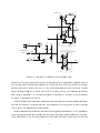
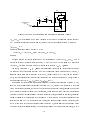
We illustrate the types of wiring capacitances that contribute to the voltage of a oating wire with the help of
Figure 1. In this gure an example of an interconnect open is shown. C5 denotes the total wiring capacitance
from oating wire FW to the n-wells and to the VDD supply wires. C6 is the total wiring capacitance from
FW to the substrate and to the GND supply wires. C3 and C4 denote the wire-to-wire capacitances from
FW to neighboring signal wires, which are created by metal tracks running next to, over, or under FW .
The sizes of C3 , C4 , C5 , and C6 together with the voltages on signal lines S 3 and S 4 contribute to the
determination of the voltage on FW . The meanings of Vsurf and Csurf are discussed later.
One needs to know the exact location of an open in the interconnect in order to obtain the list and
sizes of wiring capacitances to the corresponding oating wire. If an open is going to occur on a piece of
2