1
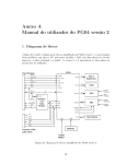
*****************************************
*
*
*
HYTEC ELECTRONICS LTD.
*
*
*
*
SCA 1270 SYSTEM CRATE ADAPTOR
*
*
*
*
MODULE SPECIFICATION
*
*
*
*
AND TECHNICAL MANUAL
*
*
*
*****************************************
HYTEC ELECTRONICS LTD.
5 CRADOCK ROAD, READING, RG2 0JT, U.K.
Doc:
Issue:
Date:
Author:
UM1270
4.0
09/01/2002
PJM
Doc:
Issue:
Date:
Page:
Author:
CONTENTS
1.
Introduction
2.
Principles of Operation
Figure 1:
Example System Configuration
3.
CAMAC Command Set
4.
Physical
5.
Circuit Description
5.1
Data Buffers and Register
5.2
Command Register and Output Drivers
5.3
CAMAC Command Decode PAL and Control PAL
5.4
Priority Arbitration Circuitry
5.5
Reset and Booking Circuit
5.6
Status Register
5.7
Control Register
6.
Parts List
7.
Circuit Diagram
- HL1031
UM1270
4.0
09/01/2002
1
PJM
Doc:
Issue:
Date:
Page:
Author:
1.
UM1270
4.0
09/01/2002
2
PJM
Introduction
There have always been lengthy discussions within Hytec Electronics Ltd.
whenever a new Controller is being designed as to whether it should be Hytec
System Crate or ACB (Auxiliary Control Bus) compatible. When the 1330 IBM PC
Interface was conceived, its principal application was thought to be in Single
Crate Dedicated Systems, so to avoid extra cost and complexity it was decided to
make it an ACB device (either Master or Auxiliary). When the 1340 List Processor
was being developed, since its concept originated in the USA, it too was made an
ACB Auxiliary Controller. Both devices are therefore fundamentally unable to
access multi-crate systems based on the Hytec System Crate method of realising
Multi-Master Multi-Crate Architectures.
Consider now the position of an Engineer wishing to add either device to a
multi-crate system based on the Hytec System Crate. He must either put one of
these devices into each of the Branch crates he wishes to monitor or control as an
Auxiliary to the CCA2, or find some way of allowing his Controller to generate
Branch cycles from the System Crate. This is what the System Crate Adaptor is
designed to do.
2.
Principles of Operation
At the outset, since the ACB device will reside in the Hytec System Crate,
the Executive Controller in that crate will have to be an MXCTR5 in order to allow
the new Controller access to the crate. (The MXCTR5 is a System Crate Executive
Controller with ACB Master capability).
Looking at Figure 1, we see that our Auxiliary Controller will now be able to
talk to modules in the System Crate, while the Computer Interface Program
Source(s) can talk to the Branch Crates and modules in the System Crate.
Doc:
Issue:
Date:
Page:
Author:
UM1270
4.0
09/01/2002
3
PJM
The System Crate Adaptor is a System Crate Program Source which is addressed
as a user module by the Auxiliary Controller (and anyone else for that matter) and
told what to do in terms of the Command, a 24 bit word in the form BCFNA: B
(branch), C (crate), F (function code), N (station number), A (subaddress); and
the Write Data (if any).
Having received the Command, it will then either wait for the Write Data or
start straight away trying to gain access to the System Crate via the Priority
Arbitration Highway. [For further information on the method of operation of the
System Crate see publications "Hytec System Crate Philosophy" and "Configuring
Hytec System Crate Controllers"]. Having achieved Mastership, it then does its
cycle, storing the state of Q and X from that cycle and the Read Data (if any).
If the cycle is aborted by the Executive Controller due to non-reception of
S2, or if X is not received, then the SCA will generate a LAM, provided the LAM
Enable bit is set in the Control and Status Register.
Note that once the SCA has "decided" to do a cycle, it will not accept any
commands except Read CSR - F(1) A(12); Reset - F(25) A(15) and Test Done - F(8)
A(15).
Having caused the SCA to perform a cycle, the Auxiliary Controller should
issue the Test Done command until it gets Q=1, and then either read the CSR to see
if Q and X were received in the cycle or fetch the Read Data, or neither. Clearly
it does not have to do either, if the Command was a Write Operation or dataless,
and the state of Q and X are therefore unimportant. Fetching Read Data is
conditioned by Q, depending on whether the SCA got a Q response during the cycle
in question. Bit 2 in the Status Register shows whether the SCA has "Done" the
last cycle requested, and this can also be tested by a separate command as
mentioned earlier.
Note that since the SCA will be doing a System Crate cycle immediately after
being given a Command, it is extremely unlikely that the Auxiliary Controller will
be able to do an ACB cycle before the SCA has finished, so telling it to ask the
question "have you finished?" of the SCA is a bit academic, but for safety's sake
it is recommended.
If the last Command involved writing, then writing another word of Data will
cause the same command to be repeated with the new Write Data.
If the last command was a Read, then one might wish that command to be
repeated automatically, and this can be done by setting bit 6 in the Control and
Status Register, which causes the same command to be repeated when the data has
been read out by F(0) A(0).
Doc:
Issue:
Date:
Page:
Author:
UM1270
4.0
09/01/2002
4
PJM
In Multi-user systems, we must have a means of "booking" the module, so that
competing prospective users can tell if another computer is already using the SCA
or not. This is done in the same way as in the List Processor LP1340, i.e. by a
"Test Available" command and a "Reset" command. The Q response to the "Test" F(27) A(0) - indicates whether the unit is in use, (Q=1 means "Available") and if
it was available, then it will now become Booked, and give Q=0 to all further
tests until given a "Reset" command (F(25) A(15)).
3.
Command Set
F(0) A(0)
Read DATA Register
X=1, Q="Q recd."
Note that the Q response is only valid if the last
CAMAC Command done by the SCA was a Read.
F(0) A(1)
Read Command Register
X=1, Q=1
F(1) A(12)
Read Control and Status Register
X=1, Q="Done"
CSR Format:
8
7
6
5
4
3
2
1
| Q | LE | RPT | spare | NO S2 | BUSY | X
/
|
|
|
|
\
/
|
|
|
|
|
Q Response
LAM
Repeat
Cycle
Not
X resp. of
of last cyc. Enb. Cycle
Failed
Fin. last cycle
F(8) A(15)
Test "Done"
X=1, Q="Done"
F(16) A(0)
Write DATA Register *
X=1, Q="Done"
F(16) A(1)
Write Command Register *
X=1, Q="Done"
Command Register Format:
24 23 22
21 20 19 18 17 16 15 14 --- 10 9 -- 5 4 --- 1
----------------\-----/--\-------/-\--------/\-------/\-------/
Z G CAR SR
B
C
F
N
A
-------------------------------------------------------------| |
|
|
| |
|
\
Stock Register Mode (and Serial Crate Address SC16)
| \
Crate Address Register Mode (and Serial Crate Address SC8)
|
GL Read Operation
Branch Initialise (Generate CZ)
F(17) A(12)
Write Control & Status Register *
X=1, Q="Done"
F(25) A(15)
Reset: Clear PA, reset "booked" & CSR. X=1 Q=0
F(27) A(0)
Test Available, X=1, Q=1 means "available" - and
"books" the SCA: Q=0 means "booked"
NOTE : * Means that write commands are not accepted if not "Done"
Doc:
Issue:
Date:
Page:
Author:
4.
UM1270
4.0
09/01/2002
5
PJM
Physical
The unit is a single-width CAMAC module, with two four-way LEMO connectors on
the rear panel, for the Priority Arbitration Highway cables. The 30 front-panel
LED indicators show the following:BOOKED
In use
N
ADDRESSED
)
ACTIVE
Doing a CAMAC cycle
) stretched to 20mSec
NO S2
Cycle aborted
Q
Q response from last CAMAC Cycle
X
X
"
"
"
"
"
Z
Z Cycle loaded
B4-B1
3-bit Branch Code
SR
Stock Register Mode
CAR
Crate Address Register Mode
C4-C1 3-bit Crate Address
N16-N1
Station Number
A8-A1
Subaddress
F16-F1
Function Code
G
GL Read Cycle loaded
5.
Circuit Description
5.1
Data Buffers and Register
Referring to circuit diagram HL1031, at the top on the left we see the Write
Line Buffers. These IC's 11, 12 and 13 buffer the Write lines onto the internal
bi-directional tri-state data bus, so that Command and Write Data information can
be written into their appropriate Registers. Further down on the left-hand side,
we see IC's 1,2 and 3 which are bi-directional devices which connect the internal
bi-directional data bus to the Dataway Read Lines. When the unit is being
addressed as a "User" module, these buffers feed information from either the
Command Data or Status Registers OUT onto the Read Lines. When the unit is
functioning as a System Crate Program Source, i.e. it is performing a System Crate
Cycle, these buffers either put Write Data onto the Read Lines so that the
Executive Controller can transfer it to the Write Lines for writing into the
addressed module, or they accept Read Data from the addressed module for storage
in the Data Register, ICs 6, 7 and 8. Note that there is only one Data Register,
used for both Reading and Writing, thus its contents will be either the last set
of write data given to the SCA or the last set of read data collected by the SCA.
The Data Register or Data Store itself is Clocked, or written into, by K5 (CAB,
Clock A to B) and is Read Out by K4 (GBA, Gate B to A). K5 and K4 come from the
Decoding and Control PALs, ICs 26 and 27.
Doc:
Issue:
Date:
Page:
Author:
5.2
UM1270
4.0
09/01/2002
6
PJM
Command Register and Output Drivers
The Command Register or Command Store, ICs 16, 17 and 18, has its "B" outputs
connected to front panel LED’s for indication and also to output buffers, ICs 21,
22 and 23, which place B – the Branch Code, C - the Crate Number, N - the
Station Number, A - the Subaddress and F - the Function Code onto the Dataway at
the appropriate time. Individual 7438 buffer gates drive W10 ( or SR - Stock
Register Mode), W11 ( or G - Grant GL), and C and Z (for System Crate
Initialisation) via monostable IC30. Notice how the System Crate W Line Drivers
for B,C and N on W1 to W14 are enabled by K9 (P.A. Master and notBUSY), whilst
Subaddress A and Function Code F are Driven by K8 (P.A. Master). This
distinguishes between the initial part of the System Crate cycle where BCN are
passed to the Executive Controller and the Normal CAMAC cycle which then follows.
5.3
CAMAC Command Decode PAL and Control PAL
The Decode PAL IC26 looks at the incoming F and A, when strobed by N and
notF4, conditioned by QFlag and a latched version of the "Pending" flag. The
Pending flag ensures that invalid user CAMAC commands are not accepted until a
loaded Cycle has been completed, while QFlag conditions the Q response to Read
Data Commands. The outputs of the decode PAL pass to the Control PAL, IC 27, which
decides whether to initiate a System Crate Cycle through GOPULSE and enables the
Data Buffers as appropriate through K1 to K7 which function as follows:
K1
Being Written to as a user module:
F(16) A(0) or A(1),
or F(17) A(12).
K2
Activate Read Data Line Buffers:
F(0) A(0) or A(1),
F(1) A(12), or System Crate Data IN or OUT.
K3
Data Flow from SCA TO the Read Lines:
Crate Write Data involved.
K4
Data being Read from the Data Store:
F(0) A(0)
K5
Clock Write Data into Data Store:
F(16) A(0)
K6
Data being Read from the Command Store:
F(0) A(1)
K7
Clock Write Data into Command Store:
F(16) A(1)
as above but System
Signal Functions are described in their active states as shown on the circuit
diagram. Notice how some functions of the Control PAL IC 27 may be strobed by S1
and S2, and also how BUSY, PAM (P.A. Master), DONE, RPT (Cycle Repeat), C14
(Command bit 14 = Function Code 16) and C13 (Function Code 8) are all fed to it as
inputs so as to condition its output states.
Doc:
Issue:
Date:
Page:
Author:
5.4
UM1270
4.0
09/01/2002
7
PJM
Priority Arbitration Circuitry
At the top of the diagram towards the right we see the P.A. IN and P.A. OUT
connections to the standard Priority Arbitration Circuit, which is set in motion
by GOPULSE from the Control PAL, or by an external Trigger signal. Once this
circuit has achieved Mastership of the System Crate, PAM goes high, PENDING goes
high and DONE goes low. These signals enable other parts of the circuit to assess
the progress of the current cycle as mentioned above.
5.5
Reset and Booking Circuit
Just to the left of the P.A. circuit we see the Power-on-Reset circuit,
including the Reset Command signal F(25) A(15), which combine to produce the
general signal RESET. Just below this is the Booked Flag flip-flop, set by F(27)
A(0) and cleared by RESET. The Q output of this flip-flop drives the "Booked" LED
through IC25, an open collector inverter.
5.6
Status Register
Below the P.A. Circuit is a latch, IC24, which is clocked by S2 when the SCA
is P.A. Master, and which stores the states of Q and X. It also produces a NO-S2
signal, which gets asserted at the beginning of each cycle since the latch is
cleared by the Start or GO pulse, and which will only get de-asserted when the
latch is clocked (by S2). The outputs of this latch are fed through drivers to
their corresponding front panel LEDs. When the SCA's cycle is complete, the
trailing edge of PAM clocks the "Alarm" flag, IC31 pins 2 -> 5, whose data input
is the logical OR of NO S2 (which means that an incomplete Branch cycle has taken
place, probably due to addressing a nonexistent crate) and NO X. The output of
this latch drives the LAM (L) line whenever LAMs are enabled in the Control
Register, but not whilst N is present as specified in the CAMAC specification, EUR
4100.
Just above the L Line driver are the monostables and drivers for the
"Active" (doing a System Crate cycle) and "N" (addressed) LEDs.
5.7
Control Register
To the right of the alarm flag circuit is the Control Register, IC9, which
holds the four writeable bits of the C.S.R. or Control and Status Register, loaded
by F(17) A(12), two bits of which are spare (SP1 and SP2). The two functioning
bits are bit 7, LAM Enable and bit 6, Repeat. All four are returned to the Status
Register read-out buffer, IC4, which reads them back along with the states of Q
and X and the Pending and NO S2 signals in response to the command F(1) A(12). The
function of the Repeat bit is to cause the last loaded Command to be repeated
after the data from the previous cycle has been read out by F(0) A(0).
Doc:
Issue:
Date:
Page:
Author:
6.
UM1270
4.0
09/01/2002
8
PJM
Parts List
Integrated Circuits
SN7400N
SN74LS00N
SN74LS02N
SN74LS04N
SN7405N
SN7408N
SN7414N
SN74LS14N
SN74LS27N
SN74LS32N
SN7438N
SN7474N
SN74LS74N
SN74LS123N
SN74LS175N
SN74LS240N
SN74LS244N
SN74LS642-1N
SN74LS652N
Passive Components
IC35
IC15
IC29
IC36
IC25, IC32
IC37
IC33
IC10
IC5
IC14
IC28, IC34
IC31, IC38
IC20
IC19, IC30
IC9, IC24
IC11, IC12, IC13
IC4
IC1, IC2,IC3,IC21,IC22,IC23
IC6, IC7,IC8,IC16,IC17,IC18
PAL 22V10
IC26, IC27 (on sockets)
'1270P26' '1270P27'
1N5401
RED LED T1
GREEN LED T1
TIS55/MPS3646
PICOFUSE 2AMP
D1
D3,D5,D6-D31 INC.
D2,D4
TR1
FS1
100R
220R
470R
1K0
2K2
10K
.3W
R18
.3W
R5
.3W
R8
.3W
R7
.3W
R9
.3W
R1,R3,R4,R6,
R10,R12,R14,R16,R17
47K .3W
R13
68K .3W
R11,R15
100K .3W
R2
220R x 8 RES PK RP4,5,6,7
4K7 x 8 RES PK RP1,2,3
220pF CER. C5
270pF CER. C8
1n0
CER. C6
1uF 35V TANT C3,C4,C7
100uF 16V TANT C1,C2
100nF Decoupler "CD" x 45