1
HP Computer Systems
HP 98640A
7 -Channel Analog Input Interface
Hardware
Installation and Reference Manual
FIIOW
HEWLETT
~~ PACKARD
HP Computer Systems
HP 98640A
7-Channel Analog Input Interface
Hardware
Installation and Reference Manual
r!J~
HEWLETT
a!1!II PACKARD
Fli.. HEWLETT
~I!.II PACKARD
Warranty Statement
Hewlett-Packard products are warranted against defects in
materials and workmanship. For Hewlett-Packard Desktop
Computer Division products sold in the U.S.A. and Canada,
this warranty applies for ninety (90) days from the date of
delivery.* Hewlett-Packard will, at its option, repair or replace
equipment which proves to be defective during the warranty
period. This warranty includes labor, parts, and surface
travel costs, if any. Equipment returned to Hewlett-Packard
for repair must be shipped freight prepaid. Repairs
necessitated by misuse of the equipment, or by hardware,
software, or interfacing not provided by Hewlett-Packard are
not covered by this warranty.
HP warrants that its software and firmware designated by HP
for use with a CPU will execute its programming instructions
when properly installed on that CPU. HP does not warrant
that the operation of the CPU, software, or firmware will be
uninterrupted or error free.
NO OTHER WARRANTY IS EXPRESSED OR IMPLIED,
INCLUDING, BUT NOT LIMITED TO, THE IMPLIED
WARRANTIES OF MERCHANTIBILITY AND FITNESS FOR
A PARTICULAR PURPOSE. HEWLETI-PACKARD SHALL
NOT BE LIABLE FOR CONSEQUENTIAL DAMAGES.
*For other countries, contact your local Sales and Service
Office to determine warranty terms.
~. . HEWLETT
a:~ PACKARD
ATTENTION:
Users of Series 300 Computer Systems
Please read this notice berore installing card.
The HP 98640A has one application which may pose serious usage problems:
In Series 300 machines, the right angle posts which connect the ADC card to its Wire Termination
Assembly can short out on the RFI suppression shield of the processor or other card if the cards are in
adjacent slots. Since the HP 98640A must be installed in the lower of paired slots, this occurance is likely.
There are two possible solutions.
The recommended solution is to apply an insulating material (such as electricial tape) to the upper surface
of the RFI shield on the processor or other ca rd.
The second, while more difficult. is equally effective: Always place the ADC card in a slot where the
contacts are cl4early not touching any conductor. This is not always possible due to the installation
constraint mentioned above.
HP 98640A
7-CHANNEL
ANALOG INPUT INTERFACE
FOR HP 9000 SERIES 200 COMPUTERS
HARDWARE INSTALLATION AND
REFERENCE MANUAL
Card Assembly: 98640-66501
Date Codes: A-2.419
B-2.420
Fliii. HEWLETT
~~ PACKARD
HEWLETT-]PACKARD COMPANY
Roseville Networks Division
8000 Foothills Boulevard
Roseville, Callifornia 95678
ManuaIPartN~98640-90001
E0784
Printed in U.S.A
July 1984
[ PRINTING HISTORY
The Printing History below identifies the Edition of this Manual and any Updates that are
included. Periodically, update packages are distributed which contain replacement pages to
be merged into the manual, including an updated copy of this Printing History page. Also,
the update may contain write-in instructions.
Each reprinting of this manual will incorporate all past updates; however, no new information will be added. Thus, the reprinted copy will be identical in content to prior printings
of the same edition with its user-inserted update information. New editions of this
manual will contain new information, as well as updates.
FIRST EDITION ...................................................................... July 1984
NOTICE
The information contained in this document is subject to change without notice.
HEWLETT-PACKARD MAKES NO WARRANTY OF ANY KIND WITH REGARD TO
THIS MATERIAL, INCLUDING, BUT NOT LIMITED TO, THE IMPLIED WARRANTIES
OF MERCHANTABILITY AND FITNESS FOR A PARTICULAR PURPOSE.
Hewlett-Packard shall not be liable for errors contained herein or for incidental or consequential damages in connection with the furnishing, performance, or use of this material.
This document contains proprietary information which is protected by copyright. All
rights are reserved. No part of this document may be photocopied or reproduced without
the prior written consent of Hewlett-Packard Company.
Copyright (c) 1984 by HEWLETT -PACKARD COMPANY
ii
98640A Analog Input Interface
CONTENTS
Content!l ...••.........•....................•..............•...........•... iii
Preface .................................................................... vi
General Safety Con5ideration5 ..
• vi i
GENERAL ]tNFORMATION
Overview .•••••
Description ••.
Standard Product ..•
Options .•••...
Identification ..
Specification5 ... .
Electrical ... .
Functional Specifications ..
Cont",'ol .••.................
• • 1-1
1 -1
.1-2
1-2
· . 1-2
· . 1-3
· 1-3
· 1-3
• 1-4
INSTALLATION
Unpacking and Inspection ...
Caut!lons ..•.
In5pect contents.
Preparation for use ...
Calculating power requirement5 ..
Component installation ..
Boot-up ID number.
Switch Set~in9s .....
Factory Settings.
Interrupt Level ..
Inserting the card.
Where ..
How ....
Removal ..
Checking a new A-to-D card.
Attaching the wire termination aS5embly.
Cabl i nB. . . . . . .
. ...•.
Wi re ....... .
Connection ..
Removal .....
Operational Con5iderations.
Return Shipment ••..........
.2-1
· .2-1
.2-1
· .2-2
· .2-2
· .2-2
· .2-2
· .2-2
· .2-4
· .2-4
..2-5
· .2-5
· .2-5
· .2-6
· .2-7
.2-7
· .2-8
..2-8
.2-8
.2-11
.2-12
.2-13
THEORY OF OPERATION
Power and Timing.
Powelr Supply .•
System Clock .••.••.•.•.•.
....... . 3-3
· .3-3
.3-3
iii
98640A Analog Input Interface
Registers ................................................................. 3-3
])ata Registers .•.•...•....................•..•.......••...••••••.••.•••• 3-3
Pace Timi ng Regi ster •••..•••.....•..••.•.•.•.••...••.....•••.•..•••••••• 3-4
ID Regi ster ....•.•..................•................................... 3-4
Status Regi ster ..••...•......................•..............•...•....... 3-4
Analog Circui try ••.....•..............•.................•...•.........••.. 3-5
Vol tage Input ..•.•...•.•....•..........••.................•.•.•...•.•••. 3-5
Channe 1 Se 1ec t ion .•......•...••..• L' • • • • • • • • • • • • • • • • • • • • • • • • • • • • • • • • • • • • 3-6
Prograrrrnable Gai n Ampl i f ier (PGA) ..••..•••••••.....•......•..•••••...... 3-7
Gain of 1 ............................................................. 3-7
Other Gains .••.•...•...•....•....••...•.•.••.....•.•...••..•.••••...•. 3-9
Examp 1e ••••••••••••••••••••••••••••••••••••••••••••••••••••••••••••• 3-9
Di fferent ial-to-Si ngle-Ended Converter ...•..•.....•....•.••..•.•..•.••. 3-1 0
Example •••••••••••••••••••••.•.••••••••••••••.••••••••••••••••••••• 3-10
Sample and Hold (StH) Circuit •.......•.••••..••••....•••.••.••.•.•..••. 3-10
Absolute Value Circuit .•••..••........••..••.•.......••..•..••••..•..•• 3-11
Analog-to-Digi tal Converter (ADC) ......•....•.•.•....••..•.••..•.•...•. 3-12
Corrmon Mode Over range Detect ion ........•......•.......••.••.••....•.... 3-13
Digital Conversion Circuitry ...••..••...••.••....•......•..•••••.•....•.. 3-13
Generating Control Signals .........•.•.•.•••.•....••.••.•••.•••.•.....• 3-13
Stopping the Counter .••.••••.....•....••..••••••...•.•••..•.•••.•...... 3-14
Conversion Cycle Timing .....•....••.•..•....••.....•.••...•.••...••.... 3-17
The BUSY eye Ie ......................................................... 3-18
The Internal Pacing Timer •...••....•••.••••••••••.••..•.•••.•.•...•..•• 3-19
External Pacing ..•...............•........•........•..•................ 3-20
Digi tal Backplane Circui try ..•.•...••....••••.••••.....•.•....••...•..••. 3-20
Select Code ••.••••.........•••...•...••••••....•...••.••.....•....••.•. 3-20
The Backplane Handshake ••..•••...•••...•.....•••••..........•••...•..•. 3-21
Addressing .•...•.•.•..•..•..•.•...•.••...••..•.....•..•..••.•••...•.•.. 3-21
Reset!! .........•..•..•.................•.....•......................... 3-22
Backplane Data Bus ...••..•.•....••........•.••....•••••...•.••....•..... 3-22
Reading From the Card ..•...•........•..•..••••....••.........•...•..... 3-22
Wri ting to the Card .•••..•.......••.••••..•..•.•...•.••...•.•••...•..•. 3-22
Interrupt5 .•.....•........................•............................ 3-23
Sequence of Operations .....•...•....•••.....•..............••.•.•..••.••. 3-23
The Analog Pipeline •...•.....•••.•...••..•.••..•.•.........•..••.•..•.... 3-25
PROGRAMMING AND EXTERNAL PACING
Programning Considerations .•.....•.......•....••........•...•.••.•..•.•.•. 4-1
Channel and Gain ...•.•.....•.....•..•.....•..•••............•.....•.•... 4-1
Dealing wi th Data •••.•.•....•.••..•....•.....•............•....••.....•. 4-3
Calibration .•••••..•••.....••......•....•...••.........••....•..•..... 4-3
Detailed Calibration ...............•..............•..••....•........ 4-4
Qu i c k Ca lib rat ion. . • . . . • . . . . . . . . • . . • . . • . . . . . . . . . . . • • . . . • . . . • . . . . . . • . 4 - 5
Over range!! ..••.••......•...•••....••......•••.......•.•.•.••.•••..••.. 4-7
Horrra 1 mode •••••••••••••••••.•••••••••••••••.••••.•••••••••••••••••• 4-7
COlll'non mode •.•...•.....•..•........•..•....•..........•...••.•••..•. 4- 7
Simple sample •••.•.•.•.•.....•............••.•......•...••••••..•.•... 4-7
Pace Interval ..•..........................•....•...•........•....••..... 4-9
No i
Sf!! • • • • • • • • • • • • • • • • • • • • • • • • • • • • • • • • • • • • • • • • • • • • • • • • • • • • • • • • • • • • • • • • • •
iv
4 -1 0
98640A Analog Input Interface
External Pac i"9 .......................................................... 4-10
Control Line5 .......................................................... 4-11
Appl iClat ion5 . . . . . . . . . . . . . . . . . . . . . . . . . . . . . . . . . . . . . . . . . . . . . . . . . . . . . . . . . . . 4-11
Note on :8ASIC Syntax ..••.•••••••••..••...•.•..•.•.•.....•.•..•....•...••. 4-13
MAINTENANCE
Ove rv i ew. . . . . . . . . . . . . . . . . . . . . . . . . . . . . . . . . . . . . . . . . . . . . . . . . . . . . . . . . . . . . . . . . . 5-1
Preparing to test the A-TO-D card .....••........•.••••.••.•..•••••••••••.• 5-1
Mi nimunl equipment requi rement s •••..•.....•.....••..•••.•••••.•.•.•••..•• 5-1
Installing test assembly ..•.••..•••...•........•..•.....•.•.•...•..••.•. 5-1
Di5c onnecting the WT'A .........•.......•.........•.••.....•.•..•....... 5-1
I nstiall Peripherals ..•••..••...•••........•..•..•..••.•..•.••••••••... 5-2
Connecting the test assembly ..••.•.•••...•.....•...........••.•.•..... 5-2
Verification Test .........••.....••.•...•..•......•..............•........ 5-3
Ove r v i lew. . . . . . . . . . . . . . . . . . . . . . . . . . . . . . . . . . . . . . . . . . . . . . . . . . . . . . . . . . . . . . . . 5 - 3
Loading the verification program .•..•.•....•..••.•.•..•.......•....•.•.. 5-3
Sequ1ence .............................................................. 5- 3
Test~5 Performed .....................................•.........•....... 5-4
Prograrn run ............................................................. 5-4
I nsti~ lIed ADCs ....•....................•...•..........•............... 5-4
Set I~epet i t ions ...........................•................•..•....... 5-4
Pace Timer Test .•.......•.................•.........•..•.....•.......• 5-4
Select Readings to Display .............•.....•...•••..•..•....•....... 5-4
Run-Error Reporting .............................•................•.... 5-5
Succes~5ful Verification ...........•.........•..•..•..•........•.•....... 5-5
On Failure •••..........•.....•....••.......•...•........................ 5-5
Error' Codes ....................•..........•.....•..................... 5-6
1
PARTS LISTS
Organization ......................................................•....... 6-1
Ava i lab i .1 i t y .............................................................. 6-1
A-to-D card •.•.......................................................... 6-2
wire tl~rmination assembly ................•......•...•................... 6-5
test a!5sembly ...•...............................•.......•..•............ 6-6
DIAGRAMS
Resistor network ......................•....•.....•..•....•........•....... 7-2
Component Location
A-to-D card and wire term. assy ..........•..•.........•....•............ 7-3
Test a !5 s emb I y. . . . . . . . . . . . . . . . . . . . . . . . . . . . . . . . . . . . . . . . . . . . . . . . . . . . . . . . . . . 7 - 4
Schematic: diagrams
A-to-D card .........................................................•... 7-5
wi ret I:! rm. as sy ........................................................ 7 -11
t est a!5 s emb I y. . . . . • . . . . . . . . . . . . . . . . . . . . . . . . . . . . . ......•.•..•........... 7 -1 2
PROM code .................................................•............ 7-13
INADVERTANT GROUND:
A SAFETY CONSIDERATION ............••..........••..•..•. A-1
Glossary .......................................................•............ G-1
INDEX
v
98640A Analog Input Interface
PREFACE
The HP 98640A Analog Interface is designed to make putting an HP 9000 Series 200 computer in
touch with the IIreal world easy. In this manual we explain how to install the interface in your computer. We also present a very simple example of an assembly language program for making a single
reading from an input. This example, in section four, is aimed at advanced assembly language
programmers.
ll
This manual's Appendix briefly explains how the HP 98640A Analog Input Interface may affect an
existing application. A glossary follows the Appendix. Also in the back are two different reader
comment forms. One form asks you to evaluate this manual, the other asks what follow-on products
you may have a future need for.
One product that is already available is the HP 98645A Measurement Library. The library's set of
subroutines that you can call from high level languages may save considerable development time. The
following languages can call rou tines from the library:
BASIC 3.0 and 2.0 with 2.1 extensions
Pascal 3.0, 2.1, and 2.0
Contact your Hewlett-Packard sales representative for more information about the HP 98645A
Measurement Library.
We strongly recommend the following books to anyone who intends to write his or her own assemblylanguage application programs for 9000 Series 200 computers:
·Pascal 2.0 System Designer's Guide, part number 09826-90074
·MC68000 User's Manual, part number 09826-90073
If you are interested in producing applications software, ask your Hewlett-Packard representative
about HP+. We can help you get the word out about your application.
vi
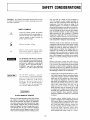
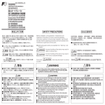
SAFETY CONSIDERATIONS I
GENERAL - This product and relation documentation must be
reviewed for familiarization with safety markings and instructions before operation,
floor can build up a charge of many thousands of
volts. The amount of static voltage developed depends on the rate of generation of the charge and the
capacitance of the body holding the charge. If the
discharge happens to go through a semiconductor
device and the transient current pulse is not effectively diverted by protection circuitry, the resulting current flow through the device can raise the temperature of internal junctions to their melting points.
MOS structures are also susceptible to dielectric
damage due to high fields. The resulting damage can
range from complete destruction to latent degradation. Small geometry semiconductor devices are especially susceptible to damage by static discharge.
SAfETY SYMBOLS
Instruction manual symbol: the product
will be marked with this symbol when it is
necessary for the user to refer to' the i nstruction manual in order to protect the
product against damage,
The basic concept of static protection for electronic
components is the prevention of static build-up where
possible and the quick removal of already existing
charges. The means by which these charges are removed depend on whether the charged object is a
conductor or an insulator. If the charged object is a
conductor such as a metal tray or a person's body,
grounding it will dissipate the charge. However, if the
item to be discharged is an insulator such as a plastic
box/tray or a person's clothing, ionized air must be
used.
Indlcatt.·s hazardous \'oltages,
Indicatt.·s t'arth 'groundl terminal Isometmlt.'s lIsed in manual to indicate circuit
('OmnlOn connt.·cted to grounded chassisl,
The WARNING sign denotes a hazard.
It calls attention to a procedure. practice. or the like. which. if not correctly
performed or adhered to. could result
in injury. Do not proceed beyond a
WA RNING sign until the indicated
conditions are fully understood and
met.
Effective anti-static systems must offer start-tofinish protection for the products that are intended
to be protected. This means protection during initial
production, in-plant transfer, packaging, shipment,
unpacking and ultimate use. Methods and materials
are in use today that provide this type of protection.
The following procedures are recommended:
1. All semiconductor devices should be kept in "antis-
CAUTION
The ('A l"rI()!\; sign d('not('s a hazard It
calls attt.·ntion to an opt'r"t ing pron·dure.
practin·. or tht.·like. which. ifnot cOITectl.\'
pl'ri'ol'llwd or adht'red to. could result in
damagt.· to or dt.·structlon of part or all of
tht.· pl'Oduct. Do not proceed heyond a
CA l'TION sign until the Indicated ·conditions are full~' undt.·rstood and met.
tatic" plastic carriers. Made of transparent plastics
coated with a special "antistatic" material which
might wear off with excessive use, these inexpensive carriers are designed for short term service
and should be discarded after a period of usage.
They should be checked periodically to see if they
hold a static charge greater than 500 volts in
which case they are rejected or recoated, A 3M
Model 703 static meter or equivalent can be used
to measure static voltage, and if needed, carriers
(and other non-conductive surfaces) can be recoated with "Staticide" (from Analytical Chemical
Laboratory of Elk Grove Village, Ill.) to make them
"antistatic. "
CAUTION
STATIC SENSITIVE DEVICES
2. Antistatic carriers holding finished devices are
stored in transparent static shielding bags made by
3M Company. Made of a special three-layer material (nickle/polyester/polyethylene) that is "antistatic" inside and highly conductive outside, they
provide a Faraday cage-like shielding which protects devices inside. "Antistatic" carriers which
contain semiconductor devices should be kept in
these shielding bags during storage or in transit.
When any two materials make contact, their surfaces
are crushed on the atomic level and electrons pass
back and forth between the objects, On separation,
one surface comElS away with excess electrons (negatively charged) while the other is electron deficient
(positively chargt~d). The level of charge that is developed depends upon the type of material. Insulators
can easily build up static charges in excess of 20,000
volts. A person working at a bench or walking across a
vii
Individual devices should only be handled in a
static safeguarded work station.
:3. A typical static safeguarded work station is shown
below including grounded conductive table top,
wrist strap, and floor mat to discharge conductors
as well as ionized air blowers to remove charge
from nonconductors (clothes). Chairs should be
metallic or made of conductive materials with a
grounding strap or conductive rollers.
BEFORE APPLYING POWER. - \'erif~' that the product is
(:onfiJ,.rurt'd to match thl' a\'ailahll' main power source per tht'
input powt'r confj~urati()n in"tructions provided in this manual.
If this product is til hI' l'lll'rl-:ll.l'd \1;\ an auto-transf()rmer tfor
\"oltClgt' n,duct ion I milk!' sun' tIll' wmmon tl'rminal is connected
til tht, l',II1h (t'rminal
of
tht,
Illalll
powt'r
SCHliTt'.
SERVICING
Any servicing. adjustment. maintenance. or repair of this product must be performed only by
qualified personnel.
Adjustments described in this manual may be
performed with power supplied to the product
while protective covt'rs are removed. Energy
available at many points may. if contacted. result in personal injury.
Capacitors inside this product may still be
charged even when disconnected from its
power source.
To avoid a fire hazard. only fuses with the required current rating and of the specified type
(normal blow. time delay. etc.) are to be used for
replacement.
'iU·';U"hi
SAFETY EARTH GROUND - This is a safety class I product
and is provided with a protl,('ti\'t' l'arthin~ terminal. An uninterruptihle safet~· l'arth ground must Ix- provided from the main
power sourn' to tht, produ(·t input wirin~ terminals, power cord.
or supplied pOWt'r cord set. Wht'fl('\'t'r it is likeiy that tht' protection has Ix-t'n impairt'd. thl' product must be madt' inoperative
and nt, ,.;t'(·un·d against an~' unintl'ndt'd operation.
EYE HAZARD
Eye protection must be worn when removing or
inserting integrated circuits held in place with
retaining clips.
viii
GENERAL INFORMATION
IF'!'H',
OVERVIEW
The HP 98640A 7-channel Analog Input Interface is an analog-to-digital converter (ADC) for
Hewlett~Packard 9000 Series 200 computers. On each HP 98640A 8 analog channels are available
for measuring small differential voltages with 13-bits resolution (including sign-bit). We call the HP
98640A a 117 -channel" interface because in applications where an input offset voltage is less tolerable
the two leads of one channel may be shorted together and grounded. The reading from the shorted
channel serves as a reference you can use to correct readings made on the other channels.
The HP 98640A can sample its inputs in any order. You can control the amount of time between
readings by programmatically setting the interface's pace timer. The interface will then do the pacing
automatically. It can send an interrupt to the computer when a sample h'as been taken. Even the
voltage range for a channel can be changed between samples. The maximum voltage for inputs is plus
or minus 10 volts. The minimum full-scale voltage range is plus or minus 19.5 millivolts. The maximum differential voltage measurable is plus or minus 9.99756 volts (best case) at a gain of 1 (full scale
voltage minus one least significant bit (Isb) value).
The interface's four input voltage ranges will accommodate signal sources ranging from control circuits to thermocouples. The voltage ranges are determined by the amplification of the input voltage
by the card. Y--ou can select any of 4 gains for any channel. The four gain factors are 1, 8, 64, and
512. This allows the ADC integrated circuit (IC) on the card to always see a voltage between 0 and 10
volts.
The rest of this section describes the interface and includes the operational specifications.
DESCRIPTION
The HP 98640A is actually two printed circuit assemblies (PCA). The main PCA is the A-to-D card
which includes the analog-to-digital converter, programmable gain amplifier (PGA), pace timer, and
backplane interface circuitry. Unlike most interface cards for 9000 Series 200 computers, the cover
plate is not attached to the main card. Instead, the plate is is attached to the second PCA.
The second peA plus the attached cover plate is called the wire termination assembly (WTA). On this
PCA are the wire termination blocks, input protection circuitry, and the control inputs for external
pacing. The wire termination blocks accept individual solid hook -up wires up to 18 gauge. Each wire
is clamped in a termination block's receptacle by turning a setscrew. The cover plate attached to the
PCA has two captive thumbscrews (dog bolts) to secure the entire assembly to the back of the computer. The main PCA should never be operated unless a WTA or test assembly is attached.
1-1
98640A Analog Input Interface
NOTE
Additional wire termination assemblies may be ordered.
By using several assemblies you can readily switch between several predetermined wiring arrangements. The
assembly's part number is 98640-66502. Contact your
HP representative or Hewlett-Packard's Corporate Parts
Center (CPC) to place an order.
Also on the wire termination assembly are 9 termination receptacles tied to chassis ground and one
receptacle tied to a low current (less than Sarna) +5 volt source, for use with the external control inputs. THIS +5 VOLT SOURCE IS NOT INTENDED FOR USE AS A POWER SUPPLY. The termination receptacles are listed in Section II.
STANDARD PRODUCT
When the HP 98640A was ordered one of three options had to be specified. The option specified
determines what equipment you received. When you unpack the cards you may want to refer to the
following lists:
Standard Product
•
•
•
•
•
A-to-D card, part number 98640-66501
Wire termination assembly (WTA), part number 98640-66502
Test assembly, part number 98640-67950
This installation manual, part number 98640-90001
Verification option (only one may be selected)
Options
VERIFICA TION OPTIONS
001 - Deletes test assembly
630 - Adds verification software on 3.5 inch disk, part number 98640-13301
655 - Adds verification software on 5.25 inch disk, part number 98640-13601
IDENTIFICA TION
Five digits and a letter (98640A) identify the Analog Input Interface. As with most Hewlett-Packard
products used with 9000 computers these five digits identify the product. The letter suffix represents
the revision level of the product.
The main printed circuit assembly or PCA (printed circuit board with all components in place) is
identified by a part number (also called a card assembly number) followed by a date code. On the
1-2
98640A Analog Input Interface
A-to-D card the part number is on the component side near the right-angle posts. The part number is
98640-66501. The line of characters below the part number is called the date code. It identifies the
circuit (by letter) and electrical characteristics (the four-digit encoded date). If there is a suffix (typically a lower-case letter») it identifies additional revisions to the PCA.
If the date code on the A-to-D card does not correspond to the date code printed on the title page of
this manual) there are differences between the interface described in this manual and the Analog
Input Interfa.ce you have received. Contact your nearest Hewlett-Packard Sales and Service office
(listed at the back of this manual) for manual update information.
SPECIFI<:A TIONS
ElectricaJ
Power Requiirements:
.672W (@
.228W (@
+ 2.570W (@
3.5 Watts
+12V)
-12V)
+5V)
total
Input overvolltage protection: Transorbs redirect voltage in excess of ± 15 volts to ground.
Input resistance, each channel: 1OOmegohms (power on)
WARNING
Each input is routed through a 1k (one thousand) ohm
resistor to ground when the power is off..
Functional Specifications
On-board clock: 1.667Mhz
Resolution of Internally clocked Pace rate: 600 nanoseconds
Sample and hold aperture time: 25 nanoseconds
Time from first Read to Hold at 55k samples/second: 7 microseconds
Minimum sample cycle: 18usec.
Linearity: 0.02% of full scale
Temperature coefficient for voltage offset: 10 microvolts per degree centigrade.
Common-mo.le rejection ratio (CMRR): 90db @ 60hz
1-3
98640A Analog Input Interface
Input voltage ranges: These ranges only specify the voltages acceptable at a particular gain. The
differential voltage between a channel's inputs should not equal or exeed full scale (see below).
1
1
1 INPUT VOLTAGE RANGE
1
------------1-----------------------1
GAIN
1
1
1
1
+ to - 10V
1
8
1
+ to - 1.25V
1
64
1
1
1
1
+ to - 156mV
1
512
1
1
1
1
+ to - 19.5mv
1
Other sampling characteristics are listed in table 1-1.
Control
Minimum external trigger pulse width: 2.3 microseconds
Trigger voltage: +2 to +50volts (trigger voltage must not go below ground)
1-4
98640A Analog Input Interface
Table 1-1
SAMPLING CHARACTERISTICS
GAIN
64
1
8
±10V
±1.25V
±156mV
±19.5mV
2. 44mV
305uV
38.1UV
4. 77uV
RMS NOISE*
STD DEVIATION
5mV
600uv
lOOUV
18uv
OFFSET AFTER
CALIBRATION
(WORST CASE)**
±7.3mV
±915uV
±152UV
±24uv
ACCURACY AFTER
CALIBRATION
(WORST CASE)**
±18mV
±3mV
FULL SCALE
LSB
INPUT
AMPLIFIER
SLEW RATE
MAX. SAMPLE
RATE (ACHOSS
CHANNELS)
MAX. SAMPLE
RATE (ON A
SINGLE CHANNEL)
400mV/usec
50mV/usec
±250uV
4mV/usec
512
±75uV
40uV/usec
20k/sec
20k/sec
14k/sec
lk/sec
55k/sec
55k/sec
55k/sec
55k/sec
* By averaging readings noise can be reduced to less than one least significant bit (Isb).
** These figures are based on an HP 98640A whose data were processed and controlled
by routines from the HP 98645A Measurement Library. The accuracy figures show
the worst case affects of noise after the library's noise reduction routine is used.
1-5
INST ALLATION -
"-_ _ _ _ _ _ _ _----r[[]
UNPACKING AND INSPECTION
The procedures for unpacking this interface are described below. Please follow these procedures to
preserve your rights under the laws governing freight shipments and to protect the hardware. You
will find these procedures in many Hewlett-Packard hardware manuals.
Look for obvious signs of damage to the package. If the outside of the box is damaged or has water
stains, or the box rattles, contact the carrier. Ask that a carrier's agent be present when you open the
box. If there is no obvious reason to have the carrier's agent present read the cautions below and on
the box before proceeding.
Cautions
Please read "Safety Considerations" at the front of this manual, especially the portion dealing with
static electricity.
CAUTION
The A-to-D card (see figure 2-2 for an outline drawing
of this card) contains static sensitive devices. Use antistatic handling procedures when working with it.
When you re:move the A -to-D card from its packing material handle it by the edges or the plastic
levers (extractors) in the corners next to the right-angle posts. Do not touch the gold-plated contacts
at the end of the card opposite the right-angle posts. If you do get a fingerprint on the gold-plated
contacts or the right-angle posts, clean them with a lintless tissue moistened with a small amount of
isopropyl alcohol.
CAUTION
Never clean the contacts or the right-angle posts with
an abrasive cleaner such as an eraser because the plating
may be damaged.
Inspect c:ontents
Check the contents of the package to verify that you have received the product and options you ordered. Refer to the description of the Standard Product and options in Section I, and your invoice. If
any parts appear to be missing, notify your Hewlett-Packard Sales and Service office.
Inspect the contents carefully for hidden damage such as detached components, corrosion, or cracks
and dents. Notify the carrier who delivered this product and your Hewlett-Packard Sales and Service
office if you find any damage. Save the packing material for the carrier. A representative at our
Sales and Service office. will arrange for repair or replacement without waiting for the settlement of
the claim against the carrier.
2-1
98640A Analog Input Interface
PREPARATION FOR USE
Calculating power requirements
Check your computer system manual to find how much power (in watts) is available from the computer's power supply at each voltage the supply provides. Add the power requirements at each voltage
for all of the cards you already have in the computer. Then add the power requirements of each
A -to-D card you will install to the totals.
If the power required at any voltage is greater than the power supply's rating at that voltage, you
must make some adjustment to your computer. Either reconfigure your system by omitting unnecessary cards or arrange to buy bus expanders through your Hewlett-Packard Sales and Service office.
Component Installation
There are no loose components to install on the A -to-D card or the wire termination assembly.
Boot-up 10 number
The 10 number of the card is a feature required by the operating system. The 10 register on the card
is hardwired to respond, "18", when polled during system boot-up. The operating system also checks
the address (which we will explain how to set below) of the A -to-O card. The 10 number and address
are used by the operating system to associate the card with an application program.
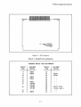
SWITCH SETTINGS
The A-to-D card has a DIP (dual in-line package) block of switches (SWl) located as shown in figure
2 -1. Switch numbers are on the switch block. These switches control the card's address and the
priority level of any interrupt the card transmits. You must select part of the address for the card.
The portion of the address you set on switches 1 to 5 is called the select code. The remainder of the
address is already hardwired. If you use a program which requires the card to send a specific level
hardware interrupt to the system, you must set the interrupt level the card will send before you install
the card in the computer. Figure 2-1 shows the switches set as they are when the A-to-O card leaves
the factory; the select code is 18 and interrupt level is 3.
The logical state of any switch corresponds to the numbers 0 and 1 silked -screened on the card just to
the right of the block of switches (SW 1). To set a specific select code or interrupt level just set the
switches to the logical states shown in Table 2- 2. When a switch is closed, the bit it controls is low
(logical zero). When a switch is open, the bit it controls is high (logical one). You can use your fingernail or the tip of a ball-point pen to change a switch's setting.
2-2
98640A Analog Input Interface
I
I
SW1
-
7654321
--.....IDDDDDDDI~
ON
Figure 2-1. SW 1 Location
Ta ble 2-1. Standard device assignments.
STANDARD SELECT CODE ASSIGNMENTS
SELECT
CODE
ASSIGNED
DEVICE
SELECT
CODE
8
9
10
11
12
13
14
15
98624
98626
19
20
21
22
23
24
25
26
27
28
29
30
31
16
17
18
98623
98622
98625
CUSTOM
I/O #1
CUSTOM
I/O #2
98640
2-3
ASSIGNED
DEVICE
98628
98629
98627 COLOR
(color cont.)
98640A Analog Input Interface
Factory Settings
NOTE
When using BASIC or Pascal you must use a select code
of 8 or higher. Codes 0-7 are reserved for the languages'
internal input/output system.
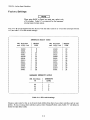
The A -·to-D card is shipped from the factory with the select code set to 1 8 and the interrupt level set
to 3 (see table 2-2 for the switch settings).
INTERFACE SELECT CODES
SW1 Switches
msb 12345 Isb
SELECT
CODE
01000
01001
01010
01011
01100
01101
01110
01111
10000
10001
10010
10011
8
9
10
11
12
13
14
15
SW1 Switches I SELECT
msb 12345 Isb I CODE
---------------+--------
----------------+---------
10100
10101
10110
10111
11000
11001
11010
11011
11100
11101
11110
11111
16
17
18
19
20
21
22
23
24
25
26
27
28
29
30
31
HARDWARE INTERRUPI' LEVELS
SWl Switches
INTERRUPl'
LEVEL
76
---------------+-----------3
00
01
10
11
4
5
6
Table 2-2. SWI switch settings
Choose a select code for the A -to-D card which differs from that of any other interface card in your
system. If you are using other interface cards at their IIstandard ll select codes, Table 2-1 will help you
locate the open select codes.
2-4
98640A Analog Input Interface
Interrupt Level
Switches 6 and 7 control the priority level of the interrupt the card can generate. The interrupt level
must be set before the card is installed in the computer. See table 2-2 if you need to set an interrupt
level that differs from the factory setting of 3.
INSERT'ING THE CARD
Where
CAUTION
Before inserting the A-to-O card be sure the computer
or bus expander where you are going to install the card
in is turned off. Any peripherals attached to the computer or expander box should be turned off also.
Refer to figure 2- 2 while reading this explanation. Remove the cover plate from the computer that
covers the accessory slot where you intend to install the A -to-O card. The card must be installed in
any of the odd numbered card slots in the card cage of your computer. An odd-numbered slot is a slot
just below the threaded mounting holes for a cover plate. Unlike many I/O devices for 9000 Series
200 computers, a cover plate is not attached to the A -to-D card so you can actually seat the card in
the wrong slot.
How
To install the A -to-D card pickup the card by the corners where the extractors (plastic levers) are attached. Be sure the component side of the card is up. Check for any fingerprints on the contacts of
the top (c01nponent side) and bottom of the card. Clean the contacts, as necessary, with a non -abrasive
cleaner. Make a final check that the switches are set correctly.
I CAUTION I
The pressure required to seat the A -to-O card may be
sufficent to cause some 9000 Series 200 computers to
move.
Now, line up the card with the grooves in the card cage and begin to gently push the card into the
grooves. Push until about one-half inch (ISmm) of the A -to-D card projects from the card cage. Let
go of the card, fold the extractor levers flat against the card and use your thumbs to push the card
into place with a firm, even pressure. If you push on the extractors there is less of a chance you will
accidentally damage one of the right-angle posts.
WARNING
THE RIGHT-ANGLE POSTS ARE SHARP ENOUGH
TO CUT YOU IF YOU PUSH ON THEM.
2-5
98640A Analog Input Interface
~
~
A-to-D
THREADED HOl
~
CARD~~
MA TING CONNECTORS
~
RIGHT -ANGLE POSTS
~'
/
EXTRACTO~~~ ~
WIRE TERMINA TION ASSEMBLY
Figure 2 - 2. Installation
The A-to-D card must seat in order for the wire termination assembly to fit on the back of the computer. When correctly installed the card's extractors will be folded flat against the card with one edge
of each extractor touching or almost touching the card cage.
Removal
I CAUTION I
The following instructions for removing the A-to-D
card assume you have properly powered -down the computer and removed the wire termination assembly as explained
in
Section
5
under
the
heading
"DISCONNECTING THE WTAII. If you have not turned
the power on yet, then the instructions below apply.
2-6
98640A Analog Input Interface
To remove the A -to-D card, pull the edge of the extractors nearest the right-angle posts outward. As
the extractors swing outward their tips will pivot against the card cage and jack the card free of connectors at the other end. When the card is free of the connector, grasp the corners of the card and
slowly slide it out of the card cage.
Checking a new A-to-D card
This is a good time to checkout the card's operation--before the wire termination assembly is attached. See Section 5 under the heading "Preparing to Test the A-to-D Card". Once you have
verified the card is operating correctly, return to this section for an explanation of installing the wire
termination assembly.
ATTACHING THE WIRE TERMINATION ASSEMBLY
Refer to figure 2-2 for help installing the wire termination assembly. Pick up the wire termination
assembly and orient it such that the thumbscrews line up with threaded holes in the card cage and the
mating connectors for the right-angle posts on the A-to-D card are also lined up.
Push the cover plate forward until the mating connectors engage the posts and the thumbscrews just
enter their respective holes in the card cage. Tighten both screws simultaneously or they may bind.
Tighten until the cover plate is seated against the card cage's outside edges. Tighten only finger tight;
over-tightening may strip the threads of a thumbscrew or the card cage.
I CAUTION I
The right-angle posts must properly engage the mating
connectors on the wire termination assembly. There is a
connector for every post and no extras. The A-to-D card
and/or the wire termination assembly may be damaged
if power is applied with a post shorted to the cover plate
or in the wrong receptacle of the mating connector.
If the thulmbscrews bind do not force them. Unscrew the assembly and try again. If, after several trys
you are unable to seat the cover plate you may have defective screws. Please contact the nearest
Hewlett-f1ackard Sales and Service office. If the thumbscrews are defective, we will help you obtain a
replacement wire termination assembly. Do not attempt to substitute conventional screws for the
thumbscrews as you will void your warranty and may damage the card cage.
I CAUTION I
The A-to-D card may be damaged if the entire Analog
Input
Interface
is
not
properly
installed.
Hewlett-Packard will not support an improperly assembled Analog Input Interface. You must operate the
A -to-D card with either our wire termination assembly
or our test assembly installed.
2-7
98640A Analog Input Interface
The wire termination receptacles on the wire termination assembly are arranged as shown in figure
2-3. You can open the throat of each receptacle by turning the screw above that receptacle counterclockwise (as viewed from above) with a small, straight-bladed screwdriver.
CABLING
Wire
Since the HP 98640A Analog Input Interface measures differential voltage there must be at least two
conductors coming from the voltage source you will measure. Your voltage source should have its own
ground reference in any circuit that includes the interface. Where desired shielded cable may be used
for the hook -up. For easy hook up to the wire termination assembly, we recommend insulated solid
wire of any American Wire Gauge (awg) between 28 to 18 inclusive. Stranded wire may be used but
should be tinned with solder to hold the strands together.
NOTE
You must provide strain relief for the wires attached to
the wire termination assembly. The wire termination assembly is not designed to support the weight of a large
cable or long lengths of individual conductors.
Connection
WARNING
THIS INPUT INTERFACE WILL APPEAR TO BE A
LOW-RESISTANCE PATH TO GROUND FOR ANY
VOL T AGE MORE THAN I 5 VOL TS ABOVE OR
BELOW GROUND.
WHEN POWER TO THE COMPUTER IS TURNED OFF
EACH INPUT IS SHORTED TO GROUND THROUGH
A ONE THOUSAND OHM RESISTOR REGARDLESS
OF THE VOLTAGE ON THE INPUT.
Open the throat of the receptacle where you will install a wire by turning the screw above the opening counter-clockwise (as viewed from from above). Set the wire you will use in your strain-relief
device but leave enough slack to reach the termination assembly and allow for stripping the wire.
Strip between one-quarter and 9/32 inch (6 to 7 millimeters) of insulation from the end of the wire.
Insert the bare wire into the receptacle and turn the screw clockwise (as viewed from above) until the
wire is held firmly. Do not over tighten the screw as you may damage the termination block or the
slot in the screw's head.
2-8
9 8640A Analog Input Interface
--
.(!]]I[
1000.-
----
r--
<D
CD
<D
<D
CD
i
I
COMPONENT
SIDE
I
II:
I
-
-
<D <D
<D
<D
<D
<D
<D <D <D
<D
<D
<D
<D <D
<D
<D
<D <D
<D <D <D
<D
~
<D
<D
<D
i-...-
-
1.
2.
3.
4.
5.
6.
7.
8.
9.
10.
11.
12.
13.
14.
15.
16.
17.
18.
19.
20.
21.
22.
23.
24.
25.
26.
27.
28.
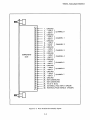
GROUND
- INPUT } CHANNEL 0
+ INPUT
GROUND
-INPUT}
CHANNEL 1
+ INPUT
GROUND
-INPUT}
CHANNEL 2
+ INPUT
GROUND
-INPUT}
CHANNEL3
+ INPUT
GROUND
-INPUT } CHANNEL4
+ INPUT
GROUND
-INPUT}
+ INPUT
CHANNEL5
GROUND
- INPUT } CHANNEl.. 6
+INPUT
GROUND
- INPUT } CHANNEL 7
+ INPUT
GROUND
NOT CONNECTED
NOT CONNECTED
+5V @
50ma
29. EXTERNAL PACE INPUT (EPCON)
30. INTERNAL PACE DISABLE (lPACDA)
<
,.--.
m
I.......-
-
"---
Figure 2- 3. Wire termination assembly inputs.
2-9
98640A Analog Input Interface
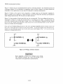
Figure 2-·4 shows the two recommended hook ups for a reference channel. Any channel may serve as
a reference channel. If you determine by experiment that the offset voltages on an input channel are
acceptable in your application, you can use all 8 channels for making measurements.
Figure 2-·5 shows a few ways to wire a channel so a voltage source can be measured. Appendix A
shows a possible circuit application. There are many circuits into which the interface can be added to
make voltage measurements. We will not try to list them here.
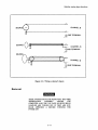
Figure 2-6 has examples of hook -ups which are not recommended. The two problems the wiring arrangements in figure 2-6 cause are ground-loops or over voltage on an input. A ground-loop will
contribute unwanted noise to the input voltage. Also, if the difference in potential between chassis
grour:d and the voltage source's ground is high enough, the current limiting resistor on the wire termination assembly may be damaged.
Once you have finished adding the wires to the wire t.ermination assembly and the voltage sources you
may '''Vish to use cable ties to form the wires into bundles. If you have several wire termination assemblies you can fabricate several wire bundles allo\\ ing a rapid change of the 7 or 8 circuits you are
making your measurements from.
+
+
CHANNEL
9
I
11
CHANNEL
GND TERMINAL
GND TERMINAL
r-h
I
11
I
rT7
I
1"
Figure 2-4. Wiring a reference channel.
CAUTION
Read Appendix A before you configure your system.
The resistance between any input and ground is low
when the A -to-D card's host is powered down.
2-10
98640A Analog Input Interface
~?7 GND TERMINAL
I , ,
SOURCE
C=!===========3(3C~ ~
CHANNEL ."
OGNDTERMINAL
I
,rl-7
,,
SOURCQE
C:
':;6I~=)~J===-=--=--=--=--=--=--=--=--=-__~(~_---lJ~1
CHANN EL 7]
Q GND TERMINAL
/l7
Figure 2-5. Wiring a channel's inputs.
Removal
WARNING
THESE INSTRUCTIONS FOR REMOVING THE WIRE
ASSEMBL Y
ASSUME
THE
TERMINA TION
COMPUTER AND THE VOLTAGE SOURCES BEING
SAMPLED ARE TURNED OFF. IF THEY ARE NOT,
READ APPENDIX A BEFORE TURNING THE
POWER OFF.
2-11
98640A Analog Input Interface
SOURCE
$
x
0
~
'"
- OR +
CHANNEL "7
+OR GND TERMINAL
+
-=- FLOATING
=
CHANNEL"7
SOURCE
,'~,
,,
GND TERMINAL
+
SOURCE
CHANNEL "7
GND TERMINAL
Figure 2-6. Unacceptable wiring of the inputs.
Be sure there is enough slack in the wires attached to the wire termination assembly to allow the assembly to be pulled straight back. If there is not enough slack you will have to remove the wires or
release them from the strain relief.
Remove the assembly by unscrewing the two thumbscrews simultaneously to avoid binding caused by
the plate not coming off straight. Be prepared to support the wire termination assembly as the screws
run out. Pull the assembly straight back, away from the card cage, to avoid bending the the rightangle posts on the A-to-D card.
Do not use the wire termination assembly to hang up your wire bundle. The weight of the wire may
cause damage to the assembly or the wires might slip out of the receptacles.
OPERA TIONAL CONSIDERA TIONS
The bottom of the wire termination assembly is exposed; do not allow conductors to come in contact
with the bottom of the assembly when it is installed. If the computer is turned on or there is a voltage
present on one of the channels, a short-circuit may result. The current through the short-circuit may
be enough to damage the voltage source or the metal traces on the wire termination assembly, or both.
If the traces on the wire termination assembly are damaged, you may purchase a replacement through
your Hewlett-Packard Sales and Service office or our Corporate Parts Center (CPC). The part number
is given in the description of the standard product in Section 1.
2-12
98640A Analog Input Interface
RETURN SHIPMENT
If any item needs repair) send it to your Hewlett-Packard Sales and Service office. Attach a tag to the
item with the owner)s name and address on it. Also) on the tag include a description of the service
needed.
Pack the product in the original packing material. Please observe the anti -static-electrical procedures
described at the front of this manual under the heading "Safety Considerations". If the original packing material is missing) you may use an equivalent commercially available anti-static packing
material.
You may a.lso have a reliable commercial packing company repack the item. Be sure to advise them
the item bedng shipped is static sensitive.
2-13
1------------------~~
THEORY OF OPERATION
[
This section describes the operation of the HP 98640A A -to-D card in considerable detail. To follow
this description you should have a good working knowledge of the operation of the DIRECT-I/O
backplane. If you need to beef up your background in this area, we suggest that you read the Pascal
2.0 System Designer's Guide (part number 09826-90074).
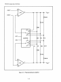
We will break our discussion down into the following topics:
Power and timing circuitry - - brief description of the power supply and the system clock.
Registers -- description of the registers that can be accessed via the backplane.
Analog Icircuitry -- description of the circuitry that transfers signals from the analog inputs to the
analog-to-digital converter (ADC).
Digital
(~onversion
circuitry - - description of the section that controls the data conversion.
Digital llackplane circuitry - - description of the backplane interface.
Sequenc.~
of operations -- summary of the interactions of the analog and digital sections; essentially
an annotated timing diagram.
Analog »ipeline -- summary of the interrelationships of successive analog readings.
Note that in this section we use the term "analog read" to refer to a read from one of the eight analog
input channels on the A -to-D card, as contrasted with a read (or write) from (or to) the status, ID, or
pace timing register.
In our discussion we will frequently refer to integrated circuits (ICs) by their "U" numbers. These U
numbers can be found on the schematic diagrams of the card (in Section 7 of this manual) and in the
replaceablf~ parts list (in Section 6). We will make occasional references to schematic locations by grid
numbers; these grid numbers are found on the outer edges of the schematic diagrams. Also, we will
refer to two asynchronous state machines: the BUSY state machine and the Conversion state machine.
Though running asynchronously, these state machines do influence each other.
In this section we will use the following convention for signals:
"BUSY"' indicates a signal which is positive true.
"BUSY _" indicates a signal which is negative true.
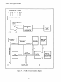
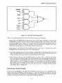
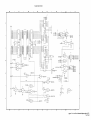
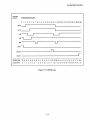
Figure 3-1 shows a generalized functional block diagram of the A-to-D card.
3-1
98640A Analog Input Interface
01 FFERENTIAL INPUTS
/
\
/
INPUT MULTIPLEXER
PROGRAMMABLE
GAIN
AMPLIFIER (PGA)
~
~I
""~__
---1
~
DIFFERENTIAL
TO
SINGLE·ENDED
CONVERTER
~--------t
SAMPLEANDHOLD
I
.I
)"2
v3
ADDRESS
LATCH
ADDR.
">L-____
ABSOLUTE
VALUE
CIRCUIT
STATUS
REGISTER
PACE TIMING
REGISTER
ADDR.
.>
---r----~
.I
v1
~
w
a:
o
o
«
16 BIT
DATA BUS
DATA
ID
REGISTER ~----"""A------t FLlP·FLOP
/
/
12
v
1
BACKPLANE
Figure 3-1. A -to-O card functional block diagram
3-2
ANALOGT()'DIGITAL
CONVERTER
98640A Analog Input Interface
POWER AND TIMING
Card Power Supply
The power that drives the A-to-D card is supplied by the host computer. The +5 volt, +12 volt, and
-12 volt supplies come off the backplane and pass through appropriate inductors and capacitors to
help stabillize the voltages. The +5 volt supply is also routed to terminal 28 on the wire termination
assembly. (This voltage is supplied for your convenience in external pacing applications; it is not intended to be a general purpose power supply.)
System Clock
The system clock signal (SYCLK) for the A-to-D card is generated by the clock chip, VI 00. Since the
clock generates TTL levels, no interface circuit is needed. The clock frequency is 1.667 MHz, or one
clock cycle every 600 nanoseonds, hence the minimum increment available for internal pacing. Note
that the clock on the card is not synchronized with the host computer's clock.
REGISTERS
To make an analog read from the A -to-D card, you must specify a register address in your read
request. The register address encodes the channel you want to read, and the gain at which you want to
read it, in the following way:
ChannE!l
0
1
2
3
4
5
6
7
Address for
gain of 1
Address for
gain of 8
64
66
68
70
72
74
76
78
80
82
84
86
88
90
92
94
Address for
gain of 64
96
98
100
102
104
106
108
110
Address for
gain of 512
112
114
116
118
120
122
124
126
For example, if you wanted to read from channel 3 at a gain of 8, you would specify a register address
of 86 in your read request.
The value returned by an analog read is the voltage for the channel and gain specified tW.!Lana)og
readu.revi~)uili. (Refer to the paragraphs on the "Analog Pipeline" at the end of this section for a
fuller explanation of this phenomenon.) The format for the returned value is:
3-3
98640A Analog Input Interface
o
15 14 13 12 11 10
9 8 7 6 5 4 3 2 1
+---+---+---+---+---+---+---+---+---+---+---+---+---+---+---+---+
IBlwlolslnlDIDIDIDIDIDIDIDlnlDIDI
+---+- .. -+---+---+---+---+---+---+---+---+---+---+---+---+---+---+
MSB
LSB
where:
B = busy. If this bit is set to 1, the card is busy; the remaining bits in the data word are invalid,and
the address provided in the read request is not accepted by the card. If this bit is set to 0, the data
word is valid and the address is latched by the address latch on the card. This bit is the inverse of bit
6 of the status register.
W = wait. If this bit is set to 1, the card is in the wait state and the analog read will not be properly
paced (according to the value programmed into the pace timing register). If this bit is set to 0, the
card is not in the wait state and the read will be properly paced.
o =common
mode overrange. This bit is negative true. If this bit is set to 0, a common mode overrange occurred during the reading; the value in the remainder of the data word is invalid. If this bit is
set to 1, no common mode overrange occurred during the reading.
S =sign. If this bit is set to 0, the voltage value in the D bits is positive. If this bit is set to I, the voltage value is negative.
D = data. These twelve bits give a binary value for the magnItude of the voltage. Bit 11 is the most
significant bit (MSB); bit 0 is the least significant bit (LSB). This is the raw value provided by the
ADC on the card; it has not been adjusted for gain.
The meanings of these bits are covered in greater detail in the remainder of this section.
Pace Timing Register
The pace timing register controls the pace interval between readings. This is a 16-bit register located
at register address 4 on the A -to-D card. To calculate the register value that corresponds to a given
pace period, use:
FFF6(hex) - round((period - 0.000018) / 0.0000006)
where period is the desired pace interval in seconds, and where round is a function that rounds a value
to the nearest integer. To place that value into the pace timing register, simply write the value to
register address 4. The A-to-D card allows pace periods from 18 microseconds to 39.3390 milliseconds, with a resolution of 600 nanoseconds.
10 Register
The ID register is an 8-bit register hard-wired with a value of 18 (the 10 number of the A-to-D
card). It is located at register address 1 on the A-to-D card. Reading from this register returns a
value of 18. Writing to this register causes a soft reset of the A -to-O card; this sets the BUSY bit to 0
and resets the PROM counter to O.
3-4
98640A Analog Input Interface
Status Register
The status register is an 8-bit register located at register address 3 on the A-to-D card. Its bits have
the f ollowi:ng meanings:
6
7
5
4
3
2
1
o
+---+---+---+---+---+---+---+---+
I I INB lINT LEVI
+---+---+---+---+---+---+---+---+
where:
I = interrupts. If this bit is set to I, the card is enabled to interrupt the CPU every time it takes an
analog reading. If this bit is set to 0, interrupts are not enabled. This is the only bit in this register
that can be written to.
NB = not busy. If this bit is set to 0, the A -to- D card is busy. The card can not accept an address
while it is in the busy state, and any voltage value read from the data register while the card is busy is
invalid. If this bit is set to 1, the card is not busy; a voltage value read from the data register is valid,
and the card can accept a new address for an analog read. This bit is the inverse of bit 15 of the data
register.
INT LEV = interrupt level. Bit 5 and bit 4 are set by switches 7 and 6, respectively, on switch pack
SW 1. These two bits show the interrupt level of the card, and indicate which interrupt line is activated when an interrupt occurs. The meanings of the bits are:
Bit
Bit
5
4
0
0
1
0
1
0
1
1
Interrupt
Level
Interrupt
Line
3
IR3
IR4
IR5
IR6
4
5
6
ANALOG CIRCUITRY
The analog circuitry on the A -to-D card takes a differential input voltage from one of the eight
analog input channels, amplifies it (if you tell it to), and prepares it for conversion to a digital value by
the analog-to-digital converter. The next several paragraphs will trace that process.
Voltage' Input
The input for the differential voltage to be measured is on the wire termination assembly that attaches to the A -to-D card proper. (The schematic diagram for this assembly is shown in Section 7 of
this manual.) The input wiring is connected to the assembly by screw terminations. The input signals
are routed to the A -to-D card proper, with overvoltage protection provided by transorbs (back -toback zener diodes) connected to ground. This arrangement limits the maximum signal going to the
card to the range of 14 to 20 volts. In addition, the analog ground of the card is protected by a
resistor and a transorb, to guard against possible hazards caused by accidental connection of a signal
line to ground.
3-5
98640A Analog Input Interface
The voltage input on the A-to-D card proper is found at location D-18 on the schematic diagram.
This is where the voltage from the wire termination assembly enters the A-to-D card. A typical input is shown in detail in figure 3-2. The input voltages enter through 1000-ohm resistors contained
in resistor arrays U61 and U71. These packs each cc;ntain 8 series resistors, and limit current to the
overvoltage protection that follows. The over voltage protection consists of two rail voltages (+ 10 volts
and -10 volts), defined by diode CR 1 for the positive side and by diode CR2 for the negative side.
Each input signal path has a reverse-biased diode connecting it to each of the rail voltages. These
diodes are contained in diode arrays U62 and U72.
+12
INPUT
-12
lKO
TO
ANALOG
MUX
Figure 3-2. Input circuit
Resistors R5 and R6 maintain current through the zener diodes to keep them in the breakdown state.
In the case of an overvoltage condition, the input voltage will exceed the zener value plus 0.7 volts.
This will forward bias the appropriate diode in one of the arrays and allow current to flow through
the zener diode. At this time the voltage at the diode array will not exceed approximately 10.7 volts
and the rest of the voltage will be dropped across the lOaD-ohm resistor. This circuit protects the inputs to the analog multiplexer (mux), U64, from overvoltage conditions at the inputs.
NOTE
The limitation on the amount of over voltage depends on
power dissipated by the 1000-ohm, 1/ 4-watt resistor: if
too much voltage is applied, the resistor will fail.
All of the analog inputs are protected in this way.
Channel Selection
Channel selection is accomplished by U64, an analog multiplexer (mux). This mux switches one of
eight differential channels into the programmable gain amplifier (POA). Its operation is controlled by
address lines AA 1, AA2, and AA3, on pins 17, 16, and 15 of U64. The differential outputs, across pins
2 and 28 go directly into the positive inputs of op amps U44 and U54.
3-6
98640A Analog Input Interface
WARNING
THE ANALOG MUX SHORTS EACH INPUT TO
GROUND THROUGH A lkOHM RESISTOR WHEN
POWER IS NOT APPLIED.
Programmable Gain Amplifier (PGA)
The PGA consists of two op amps (U44 and US4») an analog mux (U45) and a custom precision resistor
network (U24). Figure 3-3 is a diagram of the PGA) and figure 3-4 shows the innards of the precision resistor network.
The PGA selects the gain for a reading by selecting the appropriate string of resistors from the network in U24. (This selection is accomplished by the analog mux) based on the values of address lines
AA4 and AAS.) The resistor string thus selected becomes part of the feedback circuitry for the op
amps.
An op amp)s goal in life is to have its + input at the same voltage as its - input. When an op amp)s
output voltage is fed back into one of its inputs) the op amp can approach its goal (equal voltages at
the inputs) by varying its output in some suitable manner. In the case of the PGA) the differential input voltages are brought into the + inputs of the two op amps. The output of each op amp is fed back
into its - input.
GAIN OF 1
For a gain of 1) the operation of the feedback circuit for a single op amp is simple:
1) The input voltage comes in at the + input.
2) The op amp produces an equal output voltage.
3) That equal output voltage is fed directly back to the - input.
4) The 01' amp detects that the voltages at the two inputs are equal) and leaves things as they are.
The resulting stable output voltage is available for use by the next stage of the analog circuitry.
Thus) for a gain of 1) the two op amps simply pass their input voltages on to the next stage.
3-7
98640A Analog Input Interface
3
-INPUT
+INPUT
-
2
~7
V
4_2 55.5K
4-
31.5K
.28K
_1
v
_2
u
.Q.
3
(').4
--
AA4
ADDRESS
AA5
:8K
4 1K
~
.
~1
K
4
--
1)3
....,
2
1
X1
X8
X64
X 512
4:28K
431.5K
4
2
L---
3
': 255.5K
~7
V OUT +
V
Figure 3-3. Programmable gain amplifier
3-8
98640A Analog Input Interface
24
25tS~
281<
23
2
1K
8k
·22
3
255~
28k
21
4
10K
31~
5
20
1K
6
U24
10K
19
31.&1<
7
18
10K
10K ~
10K
10K
17
8
9
16
10
15
50/\
50/\
-
11
12
14
13
I
Figure 3-4. Precision resistor network (U24)
OTHER GAINS
The situation is slightly more complicated for gains greater than 1, since the resistor strings actually
connect the two op amps together. As long as there is a difference between the two inputs, the op
amps will have to adjust their outputs in order to equalize the voltages at their respective + and - inputs. When the circuit has reached equilibrium, the difference between the op amp output voltages
will have been amplified by the appropriate gain factor. Let's look at an example.
Example
Assume that your A-to-D card is connected to a device that is supplying +3.01
volts to the + input of a channel and +3.00 volts to the - input. Assume also
tha.t you are measuring that voltage at a gain of 512. The + input (pin 3) of op
amp U 54 will see a voltage of + 3.0 1 volts, and the op amp will adjust its output
until the - input (pin 2) sees the same voltage. Similarly, the + input of U 44
will see a voltage of + 3.00 volts, and the output will adjust until the - input
sees the same voltage.
3-9
98640A Analog Input Interface
In the equilibrium state, there will be a difference of 0.01 volts between the inputs of the two op amps. As a result, there will be a current of 10 microamps
flowing in the 1 kohm resistor in the feedback string. From this, we can calcula te that the voltage across each of the 255.5 kohm resistors in the string will
be 2.5 55 volts.
Thus, the output voltage from the positive op amp will be +3.01+2.555=+5.565
volts, and the output voltage from the negative op amp will be
+3.00-2.555=+0.445 volts. The differential output from the op amps is 5.12
volts, which is 0.01 volts multiplied by a gain of 512.
The only time that the PGA does not work properly is when an input voltage causes an op amp to try
to drive its output past ±10 volts. At that point the output clips and you have a common mode overrange condition.
Differential-to -Single -Ended Converter
The differential-to-single-ended converter is used to translate the differential output of the PGA to
a single-ended voltage that the Sample and Hold (S/H) circuit can handle. The gain through this converter is unity (1). The resistors in this circuit are contained in the precision resistor network (U24),
since high precision is necessary to keep the voltages accurate. Figure 3-5 is a diagram of the converter circuit.
The voltage at the positive input of the op amp (U32) is half the voltage coming from the positive op
amp of the PGA (Vin+), due to the resistive divider network in U24. Similarly, the voltage at the
negative input of op amp U32 is half way between the output voltage of U32 (Vout) and the voltage
coming from the negative op amp of the PGA (Vin-). Op amp U32 drives its output (pin 7) so that the
voltages at its negative input (pin 2) and positive input (pin 3) are equal; the resulting output voltage
equals the difference between the positive and negative voltages coming from the PGA.
Example
Consider the case where the voltages coming in from the PGA (Vin+ and Vin-)
are -3 volts and +1 volt: The voltage at the + input of the op amp is -1.5 volts.
The op amp will drive its output (V out) so that a voltage of -1. 5 volts is present
at the - input also. The output voltage thus produced will be -4 volts, and this
voltage will be sent to the sample and hold circuit.
The two 330 pf capacitors in the converter circuit act as a low pass filter, which helps to reduce high
frequency noise in the circuit.
Sample and Hold (SIH) Circuit
The S/H circuit (U 12) is used to maintain a steady voltage to the analog-to-digital converter.
Capacitor C4 is the hold capacitor for this circuit, and the BUSAMP (buffered sample) signal is the
state control signal. When BUSAMP is high, the S/H circuit is in the sample mode and the capacitor is
being charged with the voltage applied at pin 3. When BUSAMP is low, the S/H circuit is in hold
mode, maintaining the voltage that it was charged to during the sample period. The S/H output (pin
5) feeds the next portion of the circuit.
3-10
9 8640A Analog Input Interface
10K
V OU' -
10K
2
7
V OUT +
VOUT
TO SAMPLE
AND HOLD
10K
Figure 3-5. Differential-to-single-ended converter
Absolute Value Circuit
The absolute value circuit takes the voltage coming out of the S/H circuit and makes sure that it is
positive when it goes to the analog-to-digital converter (ADC). This circuit also generates a polarity
bit to indicat~~ when a negative voltage has been converted to positive. This polarity bit shows up as
the sign bit (bit 12) in the output data register. This circuit is made up of two op amps (U22 and
U23), a handful of diodes (CR3, CR4, and CR6), a capacitor (C43), and 4 resistors (R 7, R15, and two
resistors in U24). The circuit is shown schematically in figure 3-6.
The output of the absolute value circuit is driven by the more positive of the two op amps. One of the
op amps (U22) is a unity gain buffer, and the other (U23) is a unity gain inverter. Thus, one of the
outputs will always be positive. Diodes CR3 and CR4 separate the negative and positive outputs, and
cause the positive output to be sent to the ADC.
Resistors R 7 and R 15, and diode CR6 are used to generate a high logic signal if the analog input signal
is negative. The pull-up resistor (R 7) will pull the polarity signal high (+5 volts) whenever the output
of the inverting op amp (U23) is greater than 0; this will be the case whenever the analog input to
3-11
98640A Analog Input Interface
that op amp is negative. Diode CR6 prevents the op amp output from driving the polarity signal any
higher. When the analog input is positive, the inverting op amp will drive its output to the negative
rail. When this happens, current will be drawn through diode CR6 and resistors R 7 and R 15; thus, the
polarity signal will be pulled low. R 15 and R 7 will prevent the voltage of the polarity signal from
going much below ground.
The 270 pf capacitor (C43) in the feedback loop of the inverting op amp is used as a low pass filter to
reduce high frequency noise in the circuit.
+5
------ POLARITY
OUTPUT
10K
270 pf
I
10K
(S!H)OUT
I
Figure 3-6. Absolute value circuit
Analog-to-Digital Converter (ADC)
The ADC (U65) receives its analog input from the absolute value circuit and converts it to a digital
value. The converter will do a 12-bit analog-to-digital conversion in 7 microseconds; it is used in
unipolar mode to digitize a voltage from 0 to + 10 volts, with a straight binary coded output.
3-12
98640A Analog Input Interface
The data lines for the ADC are on pins 2 through 9. The output data bits are time multiplexed and
require two reads from the chip to get the full 12 bits of data. Three of the data lines (pins 7, 8, and
9) are also used as input lines to program the mode in which the converter operates.
The ADC is controlled by four control lines. The first is CHIP SELECT. Since the A -to-D chip is always selected, this line (pin 14) is tied to ground. The other three control lines are BUWR - (NOT buffered write), BURD- (NOT buffered read), and BUC/D- (buffered control/NOT data.) Signals for
these lines are generated by PROM U68 and buffered through filp-flop U67. (The signals generated
by the PROM are discussed in more detail later.) The system clock, SYCLK, is brought into the converter on pin I 3.
Four operations are carried out by the ADC chip:
Mod~9...&!"amming.
During this operation, the A-to-D card programs the A-to-D chip for 12-bit
unipolar output in straight binary coded form. To accomplish this programming, line BUWR - must
be low, lines BUC/D- and BURD- must be high, and the first three data lines must be low. The
control :signals come from the PROM (U68) via the flip-flop (U67); the data signals come from
BURD- through an inverting buffer (U 86).
Conver~.on. The conversion of the analog voltage to digital form starts when lines BUC/D- and
BUWR - go low. Once the conversion is started, it will run under control of the system clock until it
is complete; this takes 12.5 clock cycles. Since the digital conversion circuitry of the A-to-D card
runs on the same clock signals that the A-to-D chip uses, the digital circuitry simply waits an appropriatl~ number of clock cycles before requesting the results of the the conversion from the chip.
First.J!~..tuead. The ADC chip doesn't have enough data lines to output all of the data bits at once,
so two reads are needed to get the data out. The first read provides the 4 most significant bits of
converted data. This read occurs when BUC/D- and BUWR - are high and BURD- is low.
Secondjlatuead. The second data read provides the 8 least significant bits of converted data. This
happens when BUC/D- and BURD- are low and BUWR - is high.
Commc)n Mode Over range Detection
The common mode overrange detection circuit detects whether either of the op amps in the PGA is
producing an output that is greater than + 10 volts or less than -10 volts. The circuit uses 4 op amps
with open collectors, contained in package U 3 3.
The circuit works by comparing the outputs of the PGA op amps with the positive and negative voltage rails established in the input protection circuit. If one of the PGA op amps produces a voltage
grea ter in magnitude than 10 volts, one of the op amps in U 33 will detect it and turn on its open collector output, thus pulling the common mode overrange signal (OVD-) low. The state of the OVDsignal is provided in the 0 bit (bit 13) of the output data register.
DIGIT AL CONVERSION CIRCUITRY
The analog-to-digital conversions made by the A -to-D card are controlled by a state machine and associated digital circuitry. The next several paragraphs describe th~t circuitry in considerable detail.
3-13
98640A Analog Input Interface
Generating Control Signals
The control signals that drive the Conversion state machine are generated by a PROM, U68. The
PROM gets its addresses from counter U98, which is in turn driven by clock generator U 100. The
clock signal to the counter is gated through a NAND gate (U94); this allows the counter to be stopped
when the output of flip-flop U93 is low. The state of U93 is determined by the output of
AND-OR -INVERT gate U92. (The usefulness of this arrangement will become apparent presently.)
When the counter is counting, the address sent to the PROM is incremented with every clock cycle.
For each address, the PROM outputs the bit pattern that was programmed into it; these outputs are
the control signals that drive the conversion circuitry. When the PROM reaches the end of its sequence of control signals, it outputs a control signal that resets the counter and causes the sequence to
start over again. The timing diagram in figure 3-7 shows the sequence of control signals generated by
the PROM.
Flip-flop U67 buffers the output of the PROM to remove any glitches that may appear on the output
lines when the outputs change. The PROM outputs are clocked on positive transitions of the system
clock; those signals are clocked into the flip-flop on the negative transition half a clock cycle later.
Since the PROM outputs are unstable only on the positive clock edge, the control signals clocked into
the flip-flop are always clean, and the outputs of the flip-flop are always free of glitches.
The A-to-D card makes use of both buffered and unbuffered control signals. To differentiate between them, the names of the buffered signals have IIBU II added to the front of the unbuffered signal
name. For instance, the latch signal is named LACH in its unbuffered form and BULACH in its buffered form. The buffered signals are used for most applications on the card, since most devices on the
card use positive clock transitions; use of the negatively clocked buffered signals ensures that the signals will be waiting at the inputs when the positive clock transition occurs. There are, however, a few
devices on the card that make use of negative clock transitions; unbuffered signals are supplied to the
inputs of these devices.
Stopping the Counter
Each clock cycle takes 600 nanoseconds. Since there are 30 instructions in the control sequence, the
minimum time for completion of the sequence is 18 microseconds. This minimum time is attained
only in certain circumstances; there are some situations in which it is useful to stop the counter and
extend the cycle time.
Stopping the counter is accomplished by the AND-OR-INVERT gate (U92) shown in figure 3-8. The
output of this gate is driven through flip-flop U93 into NAND gate U94. When the output of U92
goes negative, the counter stops.
3-14
9 8640A Analog Input Interface
SYSTEM
CLOCK
CONVERSION STATE MACHINE CYCLE
o
1 234 56 7
is
91011121314151617 18192021222324252627282930
_____________________
I
~I
SAMP
LACH
C/O
--,.......-~
RP
WR
u
u
-,~-------------------------------------________________________
rl______________________
WAIT
PACEN
j
•
~------------------~----------------~r
START
BUSY CYCLE
S I___________
II
IA6
DTACK
[ CONVERSION STATE MACHINE MAY BE
HALTED AT EITHER OF THESE POINTS
ADDRESSG~~==~~-------
ADDRESSG~~-~~___~
BUSY
BUSY
LACH(ALSO
SEE ABOVE)
L--
I
I
Figure 3-7. Control signal timing, PROM U68 and BUSY state machine.
3-15
98640A Analog Input Interface
SYSTEM
CLOCK
CONVERSION STATE MACHINE CYCLE
o
1 234 56 7 8 9 1011121314151617 18192021222324252627282930
~
SAMP
.'-----------------
LACH
C/O
RP
1 ...-----
WR
u
u
-,~--------------------------------------_______________________
_____________________
WAIT
rl~
PACEN
~----------------~~----------------r
•
J
START
BUSY CYCLE
IA6
Slo...-.________
DTACK
II
[ CONVERSION STATE MACHINE MAY BE
HALTED AT EITHER OF THESE POINTS
ADDRESSG~~==~~-------
ADDRESSG~.--~L-____~
BUSY
BUSY
LACH(ALSO
SEE ABOVE)
L--
I
I
Figure 3-7. Control signal timing, PROM U68 and BUSY state machine.
3-16
98640A Analog Input Interface
EXTPAC
PACEN
+5
B1JSY
WAIT
GND
GND
PACEN
ENDCT
PACDA
Figure 3-8. AND-OR -INVERT gate (U92)
There are two times during the conversion cycle that the counter can be stopped:
1) ClocL~~cle~. The PROM sets the WAIT signal high at clock cycle O. If BUSY - is also high, the
output from U92 will go low and cause the counter to stop counting. This situation occurs when
the card is waiting for an analog read. As soon as the CPU removes the card address from the
backplane, BUSY- goes low on the next negative clock transition and U92 releases the counter,
which st.arts counting again on the following positive clock transition.
2)
ClocL~cle-1J. The PROM sets the PACEN signal high at clock cycle 15. This lets the counter
be stopped by an external pacing circuit or by the pacing timer.
a) An external pacing circuit will stop the counter if it holds the external pacing input of the card
high. This holds EXT PAC low, and the inverted EXTPAC input into U92 stops the counter until the external pacing circuit lets the external pacing input go low again.
b) The internal pacing timer uses the ENDCT signal to stop the counter. In this way, the pacing
timer can stop the conversion cycle to let the programmed pace interval elapse between readings. The pacing timer holds ENDCT high until the timer counts up to FFFF(hex); at that point,
ENDCT goes low and U92 releases the counter. (All this assumes that the PACDA (internal
pace disable) line remains high; this must always be the case except in external pacing situations.
Note that PACDA is controlled by you, not by the card, since it is derived from the internal
pace disable input on terminal 30.)
Conversion Cycle Timing
In the next few paragraphs we will look at the conversion cycle and the way it is controlled by the
signals coming from the PROM. You'll find figure 3-7 usefql for following this discussion. We will
refer to both buffered and unbuffered control signals; keep in mind that buffered signal transitions
actually occur one half cycle after the corresponding unbuffered transitions.
3-17
98640A Analog Input Interface
Assume that we are starting at clock cycle 0 with BUSY low, waiting for an analog read. As described
above, \\' AIT is high at clock cycle O. With WAIT high and BUSY low (BUSY-high), the counter is
stopped. When the analog read occurs, BUSY is set high, the counter is released, and the state machine
moves into the conversion cycle. As the card leaves the wait state, BURD- is pulled low. On the next
clock cycle, BUSAMP goes high. This accomplishes three things:
1) It puts the sample and hold circuit in the sample state.
2) It latches the overrange bit, the polarity bit, and the 4 most significant data bits (from the ADC)
into data buffer U7 8.
3) It clocks the address from address buffer U50 into buffer U70.
On the next cycle BUC/D- goes low, enabling the ADC to release the 8 least significant data bits and
loading the value from the pace timing register into the pace timer. LACH and BULACH go high on
the following cycle; this sets BUSY low again and clocks those 8 data bits into data buffer U77.
In the next few cycles, BURD- goes high, causing the data lines at pins 9, 8, and 7 of the ADC to go
low; BUC/D- goes high, enabling the pacing timer to start counting; and BUWR - goes low. On this
last transition, the mode of the ADC is programmed. All of this activity takes us through clock cycle
7.
At clock cycle 15 the PACEN signal is raised. This allows the counter to be stopped by either the external pace input or the internal pacing timer. This stop condition will persist as long as the external
pacing input is actuated, or until the internal pacing timer reaches full value. At that point the conversion cycle will continue. On the next cycle, BUC/D- will go low, followed by BUWR-, BULACH,
and BUSAMP one cycle later. As a result, conversion begins on the voltage held by the sample and
hold circuit; in addition, the polarity and overrange signals (POLAR - and OVD-) are clocked into the
flip-flops in U96.
After allowing time for the conversion to complete, the START signal goes high. This resets the
counter to 0, causing the PROM to start the conversion cycle over again.
The BUSY Cycle
As you might infer from the discussion of the conversion cycle, the BUSY signal plays a significant
part in controlling the conversion. It is the signal that starts the conversion cycle, or causes it to stop
in the wait state. The BUSY signal is controlled by its own state machine, which consists of two J-K
flip-flops (U 8 5) and a gaggle of gates (U 84). Figure 3-7 shows a timing diagram of the BUSY cycle.
An analog read puts a valid address on the address bus, causing ININT to go high (after the card
decodes its address via U39). The output of U46 is set on the next rising edge of the system clock, and
this gates IA6 (the analog read "flag") through U85A. TACH- subsequently goes low, causing
DT ACK - to acknowledge the command from the backplane.
Assume that at this time BUSY- is high and the card is in the wait state; this combination (BUSY- and
WAIT both high) will cause U92 to stop the counter. BUSY-will therefore gate the high output of
U85A through U84A, causing ADDRESSGRAB to go high on the next falling edge of the system
clock. When ADDRESSGRAB goes high, it clocks the address from the backplane into address buffer
U50.
When the address is removed from the backplane and IA6 goes low, ADDRESSGRAB gates a high
level through U84D, setting BUSY high and BUSY- low. This releases the counter, and the conversion
cycle continues on the next rising edge of the system clock.
3-18
98640A Analog Input Interface
BUSY- sets ADDRESSGRAB low (and ADDRESSGRAB- high) on the next falling edge of the clock.
ADDRESSGRAB- enables U85, and this situation is maintained until LACH goes high, which sets
BUSY low. Thus, BUSY is high continuously from clock cycle 0 of the Conversion state machine to
clock cycle 4.5; this allows the address to be clocked into the card and data to be moved to the output
buffers without interruption.
The BUSY signal is available to the backplane as bit 15 of the data register; BUSY-is available as bit
6 of the status register. Whenever BUSY is low, the card can accept a new address from the
backplane. The WAIT signal is available as bit 14 of the data register; if WAIT is high, it indicates
that the interval before the next analog reading will be longer than the interval programmed into the
pacing timer. (That's because the card is stopped and waiting for the next address.) Note that the
BUSY and \VAIT bits are not clocked to the output buffers (in contrast to the overrange, sign, and
data bits); the current states of BUSY and WAIT are always available, regardless of what part of the
cycle the state machine is in.
The Internal Pacing Timer
The internal pacing timer comprises four 4-bit counters, U36, U26, U47, and U48. These are set up in
series such that they will count from a programmed start value up to FFFF(hex). The counters use the
system clock as the time base, with each count taking 600 nanoseconds. When the BUC/D- signal
goes low, it loads the pacing timer with the values contained in flip-flops U37 and U49. When
BUC/D- goes high again, the pacing timer is enabled to count. It starts counting on the next positive
transition of the system clock, and counts continuously until the BUC/D- goes low again to reload the
timer.
The carry bit of the most significant counter (U 4 7) drives the ENDCT signal. This signal is used to
restart the Conversion state machine counter after the programmed pace interval has elapsed.
ENDCT remains high while the pacing timer counts up toward FFFF. When the timer reaches FFFF,
ENDCT is driven low.
A typical conversion cycle starts off with BUSY set high by an analog read. Shortly afterward
BUSAMP goes high, and BUC/D- goes low on the following clock cycle. The BUC/D- transition
presets the pacing timer with the values from flip-flops U37 and U49. On the next clock cycle
BULACH goes high, setting BUSY low. Two cycles later, BUC/D- goes high, allowing the timer to
count on positive clock cycles. Later in the conversion cycle PACEN will go high; since ENDCT stays
high while the timer is counting up toward FFFF, PACEN and ENDCT will combine to cause U92 to
stop the counter. (Yes, you must keep PACDA high, too. That's under your control. You keep.
PACDA high by keeping the internal pace disable input (IPACDA, terminal 30) low. IPACDA must
alwa~ be low unless you are doing external pacing, as described below.) The counter will remain stopped until the timer reaches FFFF; that sets ENDCT low and releases the counter to continue the conversion cycle"
The value that you write to the pace timing register to obtain a given pace period is:
value
= FFF6(hex)
-
round«period - 0.000018) / 0.0000006)
where the period is given in seconds and the round function rounds to the nearest integer. This formula compensates for the difference between when the timer starts counting (clock cycle 7) and when
PACEN goes high (clock cycle 15). Remember that ENDCT goes low when the timer reaches FFFF,
not when it rolls over to O.
Note that you can squeeze in a few extra microseconds beyond the maximum pace period indicated by
this formula if you specify a value between FFF7 and FFFF. For values in that range, the timer will
3-19
98640A Analog Input Interface
have passed FFFF and started counting over again by the time PACEN goes high. With both PACEN
and ENDCT high, the counter will stop until the pacing timer counts all the way around again and
ENDCT goes Iowa second time. (We doubt that you'll find much use for those additional counts; a
few extra microseconds don't usually make much difference when you're pacing in the 39-millisecond
range.)
External Pacing
You can use an external source to trigger the A -to-D card to take readings. This involves the use of
the external pact" control input (EPCON, on terminal 29 of the wire termination assembly schematic
diagram) and the internal pace disable input (IP ACDA, on terminal 30).
These inputs are shown at location D18 on the schematic diagram of the A-to-D card. They can be
driven by voltages in the range of +2 to +50 volts. For each input, the signal comes in through a 10
kohm resistor to the base of a transistor (Q 1 or Q2). The collector of the transistor is connected to a
pull-up resistor and to the control gate that propagates the signal to its appropriate function on the
card. When you apply a positive voltage to the input terminal, the transistor is turned on and the signal at the collector is pulled low.
The two input lines come into AND-OR -INVERT gate U92 (see figure 3- 8) as control signals
EXTPAC- and PACDA. (EXTPAC- is the inverted form of the EXTPAC signal shown on the
schematic diagram.) These signals combine with the PAC EN control signal to stop or start the
Conversion state machine at the times that are appropriate for external pacing. Ifa voltage is applied
at the external pace input, it sends EXTPAC- high. With f,XTPAC- high, PACEN will stop the
counter when it goes high at clock cycle 15 of the conversion cycle (see figure 3-7). Once stopped, the
counter will not continue until the voltage at the external pace input is removed, causing EXTPACto go low.
With this mechanism, you can control the timing of readings by controlling the external pace control
(EPCON) input. If you hold the EPCON input high and then have the CPU request an analog read,
that read will return data with the Busy bit set. The Conversion state machine will be stuck at clock
cycle 16 until you bring the EPCON input low. When EPCON goes low EXTP AC- will go low and
the Conversion state machine will continue its cycle.
When you are doing external pacing, you should keep the PACDA control signal low. (Do this by applying a positive voltage to the IPACDA input, terminal 30.) This disables the internal pacing timer
on the card and prevents the timer from stopping the state machine counter. This means that the
EPCON input (terminal 29) is the only signal that controls the release of the counter. Refer to Section
4 of this manual for a discussion of the implications of this set-up. Whenever you are not using external pacing, you must keep PACDA high (IPACDA low).
DIGIT AL BACKPLANE CIRCUITRY
The following paragraphs describe the circuits that interface with the CPU via the backplane.
Select Code
The select code circuit does two things for the card: first, it determines what the select code of the
3-20
98640A Analog Input Interface
card is; second, it compares the upper 8 bits of an address with the select code to determine whether
the card is being addressed. This function is implemented with an 8-bit comparator (U39), 5 of the 7
switches on DIP switch SW 1, and 5 of the 7 resistors in resistor pack RIO.
One side of each resistor in the SIP is tied high to form a pull-up resistor. The other side of each resistor is tied to a switch that can be closed to ground. This connection also provides the signal to drive
other devices.
Com para tor U 3 9 compares address lines A 16 through A 23 from the backplane with the select code
switches (pins 9, 7, 5, 3, and 12) and the hard-wired bits (pins 14, 16, and 18). If the two sets of signals match, and if backplane address strobe BAS- coming in to pin 1 is low, the comparator will drive
lIMA - (pin 19) low. This tells the card that it is addressed, and also enables the DT ACK - and IMAdrivers to drive the backplane.
The Backplane Handshake
When the II1\1A- signal goes low, the backplane data strobes (BUOS- and BLOS-) are enabled to drive
ININT high. The logic for this operation is shown at location B27 on the schematic diagram, using
two OR gates and a NAND gate. When ININT goes high, flip-flop U 46B will drive its Q output high
on the next rising edge of the system clock (SYCLK). One clock cycle later, that Q output will drive
flip-flop U 46A high and its Q- output will go low. This low output is designated the TACH-signal,
and it drives the DT ACK - signal on the backplane low.
When the CPU removes the card address from the backplane, the ININT signal goes low. This clears
both flip-flops in U46 and leaves the circuit ready for another I/O operation.
Addressing
The several different operations that can be done on the A -to-O card are decoded with the circuitry
at locations B to C6, 7, and 8 on the schematic diagram. Only the first 6 address lines, A 1 through A6,
are required to address the card. Because the backplane is capable of driving only one TTL load for
each input signal, most of the lower address lines go through some sort of buffer gate before they
reach a decoder or register.
Address bit 6 is used to designate an analog read (or write).
NOTE
Analog writes are emphatically NOT recommended because, if the the busy bit is low, the address data is
retained but the data from two readings ago will have
no where to go. It will be overwritten.
If address bit 6 is high and lIMA is high, signal IA6 is set high. This signal is used to disable the 3-bit
decoder at U69, to tell the BUSY state machine that an analog read is taking place, and to enable
analog data buffers U77 and U78 to drive the internal data bus.
Address bits 4 and 5 specify the gain used in an analog read. These address bits are first clocked into
address bufff~r U 50, and then into buffer U70. From there they drive the analog mux that selects the
gain of the programmable gain amplifier.
3-21
98640A Analog Input Interface
The use of address bits 1, 2, and 3 depends on whether an analog read is taking place. In the case of an
analog read (IA6 high), these bits are clocked from address buffer U 50 into buffer U70; from there
they generate the signals that determine which channel is used to take an analog reading. If it is not
an analog read (IA6 low), these three bits enter decoder U69 and cause one of its output signals to go
low. The decoder outputs combine with other signals to perform various card functions.
Resets
A reset occurs on the A-to-D card when the CPU drives the RESET- signal on the backplane low
(hard reset) or when you write to address I on the card (soft reset).
In the case of a hard reset, the RESET- signal from the backplane is buffered by an OR gate in U97.
Coming out of U97 as signal CLR 1-, it takes two paths. The first sets the interrupt enable flip-flop
(U93B) low; the second goes through NAND gate U94B and emerges as RESET. RESET makes its way
to counter U98 via OR gate U95B, and resets the Conversion state machine to cycle 0, leaving it in the
WAIT state.
A soft reset occurs when address 1 (the 10 register) is written to. This is a normal write, and the write
signal (BR/W -) comes on to the card and is buffered by A NO gate U 8 5B. The ou tpu t of this gate is
ORed with TACH- (U97C), and the result is ORed with 10- (U95C). Coming out of U95C as signal
CLR2-, this result takes two paths. In the first, it goes through NAND gate U94B and, emerging as
RESET, it travels through OR gate U95B and arrives at counter U98, resetting the Conversion state
machine to cycle 0 (the WAIT state). In the second path, CLR2- clears the BUSY and
ADDRESSGRAB flip-flops (U 83). The soft reset does not affect the interrupt control.
Backplane Data Bus
Two hi-directional buffers, U38 and U29, drive the backplane data bus. Backplane signal BR/Wcontrols the direction of the data flow. The data buffers are enabled by BUDS-, BLDS-, and IIMA-.
lIMA - must be valid for any data transfer to take place, and BUDS- and BLDS- control whether an
odd byte, even byte, or full word is transferred. The logic that implements this function is shown at
location B7 of the schematic diagram.
Reading From the Card
The gates that handle reading from the card are shown at location B4 on the schematic diagram. The
READ signal, derived from BR/W -, is brought into these gates and one of three signals, ANEN-,
IDEN-, or STATEN-, is driven low. Which signal is selected depends on the address at the time.
These three signals control which of the three data buffers drives the internal data bus.
\\,-'hen the A -to-D card receives a read command, it drives the requested data o'nto the internal data
bus inlmediately. If the address selection drives ANEN- low, data buffers U77 and U78 drive the
data bus with results from the ADC. If IDEN- is driven low, the hard-wired 10 code is driven onto
the data bus from U27. If STATEN - goes low, it drives the status bits from U28 onto the data bus.
Writing to the Card
Writes to the A -to-D card use the same decoding method as do reads from the card. The primary differtnce in approach is that during a read the card releases the data to the backplane immediately,
whereas during a write the incoming data must be clocked into flip-flops. For all writes the TACHsignal is used to clock the data in.
3-22
98640A Analog Input Interface
There are three locations that you can legitimately write to: the ID register (for a soft reset), the
status register (to enable interrupts) and the pace timing register (to set the pace interval). We've already covered the ID register in the discussion of resets, above.
There is only one bit that you can write to in the status register. That is bit 7, the interrupt enable
bit. The output from U97B (valid write) and the decoded status register address (from U69) combine
in U 81 C to produce the STSTAT signal. This clocks bit 7 from the internal address bus into the interrupt enable flip-flop, U93B. The Q output of this flip-flop is wrapped around into bit 7 of the status
register, so that the interrupt enable status is available on a status read.
Writing to the pace timing register is accomplished with the help of the TIME- signal (decoded from
the address by U69) and the "valid write" signal that comes from U97B. These two combine in U81B
to produce t.he signal that clocks the pace timer value from the internal data bus into flip-flops U37
and U49.
Interrupts
The interrupt level of the card is set by two resistors from SIP resistor pack RIO and two switches
from DIP switch pack SW 1, in the same way that the value of the select code is set. The two interrupt
level lines, INTI and INT2, drive bits 4 and S of the status register (U28) so that the interrupt level is
available on a status read. INT I and INT2 also drive the inputs of decoder U79.When interrupts are
enabled by writing to bit 7 of the status register (as discussed above), the interrupt enable flip-flop
(U93B) activates one of the two enable pins of U79. When the BUSY signal goes low, activating the
other enable pin of U79, the appropriate backplane interrupt line (IR3, IR4, IRS, or IR6) goes high,
generating an interrupt to the CPU.
SEQUENCE OF OPERATIONS
What follows is a summary of the operation of the A-to-D card. It is based on the timing diagram for
the conversion cycle, but also includes events from the BUSY cycle. You will probably want to refer
to the timing diagram in Figure 3-7 as you go through the sequence.
In the listing below, the numbers i:n front of each sequence of events indicate the conversion cycle
clock time. Note that the conversion cycle will repeat without stopping only if:
1) the CPU always supplies a new register address (via an analog read) before the Conversion state
machine enters the wait state, and
2) external pacing is not in effect, and
3) the value in the pace timing register is set for the minimum pacing interval (or, alternatively, the
internal pace timer is disabled completely).
If these conditions are not maintained, the Conversion state machine's counter will stop the conversion
cycle; the cycle will remain stopped until the condition that caused it to stop is reversed. (There's
nothing wrong with stopping the conversion counter; in many situations it's positively the right thing
to do. It's just that the timing diagrams look like they keep going continuously and don't stop for
anything.)
In this listing we will mention only "significant" events in the clock cycle. That is, we will not bother
reporting when a signal changes state solely to get back to where it started from.
3-23
98640A Analog Input Interface
Remember that the buffered control signals change state one half clock cycle after their unbuffered
coun terparts.
0.0
Start of cycle. WAIT goes high.
If BUSY - is low, the conversion cycle goes on without interruption. If BUSY - is high, the
conversion counter stops until it goes low again. (In essence, BUSY - high means that the
card is waiting for an analog read to take place. Once the analog read starts, it will take
from 3 to 4 clock cycles before BUSY-goes low again and the conversion counter starts
counting again. During that time the backplane reads the data, and the new address is
clocked into the address buffer. Two clock cycles later, BUSY-goes low, the conversion
counter is released, and the cycle continues.)
(Note that you can keep the cycle from stopping by making sure that the analog read takes
place in time for the card to be busy (BUSY - low) when the WAIT signal goes high. The
surest way to do this is to start your next analog read as soon as BUSY - goes high again.
You can determine when that happens by checking bit 6 of the status register, or by
repeatedly checking bit 15 of the returned analog data word.)
1. 0
WAIT goes low.
1.5
BURD- goes low. This enables the transfer of the 4 most significant bits from the ADC.
2.5
BUSAMP goes high. This has three effects:
The sample and hold circuit starts sampling.
The polarity bit, the overrange bit, and the 4 most significant data bits are clocked into
the internal data buffer and onto the int~rnal data bus.
The address is clocked from the address buffer into buffer U70; this drives the channel
and gain multiplexers.
3.5
BUC/D- goes low. This has two results:
It enables transfer of the 8 least significant data bits from the ADC.
It loads the value from the pace timing register into the timer.
4.0
LACH goes high.
4.5
As a result, BUSY - goes high.
BULACH goes high. This clocks the 8 least significant data bits into the internal data
buffer and onto the internal data bus.
5.5
BURD- goes high.
6.5
BUC/D- goes high. This enables the pace timer to start counting.
7.0
The pace timer starts counting. It continues counting up on every positive transition of the
clock.
3-24
98640A Analog Input Interface
7.5
BUWR- goes low. This programs the mode of operation of the ADC.
15.0
PACEN goes high. This allows the counter to be stopped by either the external pace input
or the internal pace timer.
If the external pace control input (EPCON) stops the counter, the counter remains stopped
until that input is released and EXTPAC- goes low. If the internal pace timer stops the
counter, the counter remains stopped until the timer reaches FFFF and pulses ENDCT low.
On either occurrence, the counter starts again and the conversion cycle continues.
16.5
BUC/D- goes low.
17.0
LACH- goes high. This sets up the BUSY state machine to go through its cycle when the
card receives the next analog read.
1 7.5
BUSAMP goes low. This puts the sample and hold circuit into the hold mode.
BULACH goes low. This clocks the polarity and overrange bits into their various flip-flops
and and on to the internal da ta bus.
BUWR - goes low. This starts the A -to-O conversion on the voltage held by the sample
and hold circuit.
go~s
29.5
E:USTAR T
high.
30.0
As a result, the counter resets to O. This puts WAIT high and starts the conversion cycle
over agaIn.
THE ANALOG PIPELINE
The analog pipeline is implicit in the foregoing theory of operation; now we will make it explicit. If
you follow the sequence of operations of the A-to-D card closely, you will see that the result you get
back when you make an analog read does not come from the address that you specified in tlle read; it
comes from the address that you specified two readings earlier. This is because the operations on the
card are not all serial; several operations run in parallel. This gives the effect of a pipeline: You push
addresses in at one end of the pipeline and results come out two readings later.
At any given time, the analog pipeline is working on three different analog readings. The following
table shows the events that occur in an analog read cycle and which reading those events pertain to,
assuming that you have just made the nth analog read.
READING
NUMBER
EVENT
Address
Address
Address
Voltage
Voltage
Digital
supplied from backplane
latched onto card
used to decode channel and gain
sampled at specified gain
converted to digital form
value read onto backplane
3-25
n
n
n-1
n-1
n-1
n-2
9 8640A Analog Input Interface
Why does the A-to-D card use a pipeline? Not, as you would expect, to make successive readings
happen faster. It turns out that single, non-pipelined readings could be made every 18 microseconds,
the same rate as for pipelined readings. The problem with non -pipelined readings is that they would
tie up the backplane for the full 18 microseconds, and the backplane simply doesn't allow that; two
microseconds is about all that is available at a time. By breaking the analog read process down into a
three-stage pipeline, the card can always be able to release a reading and take in a new address in that
2 -microsecond window.
Once you understand that the pipeline exists, the effect it has on the way you take readings is fairly
straightforward. For any series of readings, take two more than you need, and throwaway the data
returned by the first two.
3-26
PROGRAMMING AND -
__________
EX_T_E_R_N_A_L_P_A_C_IN_G~~
In this section we will discuss how to program the A-to-D card to make voltage measurements. We
will also discuss how to take externally paced readings.
Before you start writing assembly language programs for the A-to-D card, take a careful look at your
application. You may be able to save time and effort by writing your programs in BASIC or Pascal
and calling the subroutines from the HP 98645A Measurement Library to access the A-to-D card.
The Measurement Library subroutines are able to take readings at the full speed of the A -to-D card.
(The Measurement Library attains this speed by using the same sort of assembly language routines that
we will discuss in this section.) You might find assembly language useful if your application demands
high computational speed: an assembly language program could do the set-up for readings faster than
the Measurement Library, and it could do data reduction after the readings faster than either BASIC
or Pascal.
If you've determined that assembly language is the right language for your application, read on. We
assume that you have a, solid working knowledge of MC6 8 000 assembly language and the Pascal
operating system. (Refer to the Pascal 2.0 System Designer's Guide, part number 09826-90074, for
more information.) We also assume that you have absorbed the information in Section 3 of this
manual, particularly the paragraphs on registers and the analog pipeline.
PROGRAMMING CONSIDERA TIONS
Channel and Gain
To take a reading from the A-to-D card you must supply channel and gain information, and you may
supply pace information. The register number that you specify in your read request tells the card
which channel and gain to use for the reading. This must be a 16-bit (word-wide) read. The following table shows which register to read for a given channel and gain.
Channel
0
1
2
3
4
5
6
7
Address for
Gain of 1
Address for
Gain of 8
Address for
Gain of 64
64
66
68
70
72
74
76
78
80
82
84
86
88
90
92
94
96
98
100
102
104
106
108
110
Address for
Gain of 512
112
114
116
118
120
122
124
126
For example, to take a reading from channel 3 at a gain of 8, you would read from register 86 of the
A -to-D care:l.
4-1
98640A Analog Input Interface
The A -to-O card receives the register address on address lines A 1 through A6 of the backplane. It
decodes these lines as follows:
A 1 through A 3 specify which channel to read.
A4 and AS specify what gain to use for the reading:
A5
A4
o
o
0
1
1
0
1
1
Gain
1
8
64
512
A6 indicates whether it is an analog read. If A6 is set to 1, it is an analog read; if it is set to 0, it is
an ordinary access to the ID, status, or pace timing register.
AO is ignored. Odd-numbered register addresses are used for accessing low bytes; since only full
words are read by analog reads, odd-numbered addresses are not used. (There is no AO line on the
backplane; its function is handled by BUDS- and BLDS- which are, as the minus signs indicate,
negative true.)
For example, if your read request specified a register address of 86, the A -to-D card would break
down that address as follows:
A6
A5
1
o
analog
read
A1
AO
1
011
o
gain
=8
channel
not
used
A4
A3
A2
=3
The value returned by an analog read is the voltage for the channel and gain specified tWQ..ana]og
r£.adurevicm.~. Thus, you must take n+2 readings to get the n values that you desire. For instance,
the example program below takes 3 readings to get 1 valid voltage value. (Refer to the paragraphs on
the "Analog Pipeline" at the end of Section 3 for a fuller explanation of this phenomenon.) The format for the returned value is:
15
14
13
12
11
10
9
8
7
6
5
4
3
2
1
o
+---+---+---+---+---+---+---+---+---+---+---+---+---+---+---+---+
I BIWIOI SIDIDIDIDIDlolDIDIDIDIDIDI
+---+---+---+---+---+---+---+---+---+---+---+---+---+---+---+---+
LSB
MSB
where.:
B = busy
W = wait
o =common mode overrange (0 =overrange; 1 = no overrange)
S =sign (0 = positive; 1 = negative)
D =data
(Refer to Section 3 for a more detailed explanation of the data word.)
4-2
98640A Analog Input Interface
Dealing with Data
NOTE
Any reading that returns a I as the busy bit is invalid;
the address provided in such a reading is not latched into
the address buffers on the A-to-O card. You can ensure
valid readings by checking the busy bit (bit 15 of the
data word) or the not busy bit (bit 6 of the status word)
and making your analog read only when the card is not
busy.
The value returned in the data word is a raw reading produced by the AOC chip and the absolute
value circuit on the A -to-O card. The data word's 13 least significant bits (sign and magnitude) are
not adjusted for gain or input offset voltage. The data in the 13 bits is in signed binary form; the most
signific~nt of the 13 bits reperesents the sign (polarity) of the voltage the A-to-O card measured,
while the remaining 12 least significant bits (lsbs) are a magnitude, not a directly readable voltage.
We call these 1 3 bits the raw reading.
To change a raw reading into a voltage you could multiply the number the 12 lsbs represent by the
least significant bit value for the gain you used. Polarity is determined from the sign bit. That will
work, but the accuracy of the voltage obtained may not be suitable for your needs. You must decide,
based on experiments, if an uncorrected voltage reading is accurate enough for your needs.
One of the major factors affecting accuracy is noise. Later in this section we will devote several paragraphs to dealing with noise. Another major factor affecting accuracy is input offset voltages. We
will deal with input offset voltages here.
CALIBRAT][ON
Most of the A-to-O card's input offset voltage is caused by operational amplifiers (op amps) on the
card. You ca.n correct for most of these offsets by "calibrating" the card.
In order to calibrate the A -to-O card you will need to use one channel as a reference channel. Any
channel can serve as your reference; just short the channel's two inputs together and tie them to
ground.
Below we explain two algorithms you might use to calibrate the card. However, you can save considerable development time if you use the calibration subroutine contained in the HP 98645A
Measurement Library.
Calibrating the A -to-O card requires measuring the input offset voltage. Simply reading the
reference channel provides a gross offset value which may be acceptable in many applications. Tables
4-1 and 4-2, and the explanation of the quick calibration scheme may help you design your own
quick calibration subroutine. If you need to write a subroutine offering greater accuracy, see the
requirements for a detailed calibration. In either case, also see the discussion under the heading
IINoise" in this section.
In our explanations of calibration we use names for variables, such as Named_Variable. Since these
variable namles are to clarify procedures, no attempt was made to limit a name's length.
4-3
9 8640A Analog Input Interface
Detailed Calibration
A detailed calibration compensates for the offset introduced by the programmable gain amplifier
(PGA) and an offset effect caused by the ADC IC. The sign (polarity) of the PGA offset can be detected, but the ADC's cannot. Only the magnitude of the ADC's offset can be detected (see the theory of
operation for an expalanation of the polarity bit's origin).
To make the calibration you will need to:
1. Measure the offset caused by the ADC.
2. Measure the offset due to the PGA.
3. Apply the offsets to a reading from an input channel.
Conditions
The procedure is described below, but the sequence shown is not the only one possible. The procedure
assumes you have converted the signed magnitude to a real number. While you may perform bit
manipulations on the 13 bits of the raw reading, remember it is in signed binary (not two's compliment) form and that zero may have positive or negative sign (polarity).
The polarity of zero is caused by offsets which are too small to measure but not too small to detect.
For the mathematical operations described in the calibration procedures, normalize zero by removing
the sign.
NOTE
Most high level languages do not permit signed zero (±O)
in a numeric variable. You will have decide how to store
it.
1. ADC offset
A. Read the reference channel with the gain set to 1. With the gain set
to 1 you will minimize the affects of most offset sources except the
ADC chip.
B. Ignore the sign bit; this offset is always positive. This value is
ADC_Offset. The polarity bit you detected when you took the reading
was caused by whatever offset existed at the PGA.
2. PGA offset
A. Read the reference channel with the gain set to S12. This reading
will detect the combination of the PGA_Offset_X_ S12 (PGA offset
multiplied by S12) and the ADC _Offset.
B. Subtract ADC_Offset from the absolute value of the reading. The
difference is the IPGA_Offset_X_SI21.
4-4
98640A Analog Input Interface
C. The correct sign for PGA_Offset_X_ 512 is the same as that you
read in step 2A above. Correct the sign of PGA_Offset _X_SI2, if
necessary.
3. Application of offsets
A. Read the input channel you are interested in. Save the Uncalibrated
_Input_Reading and the gain (G).
B. Subtract ADC _ Offset from IUncalibrated_Input_Readingl (absolute value of Uncalibrated_Input_Reading). The difference is the
IPartly _ Corrected_Readingl.
C. The sign of the Partly _Corrected_Reading must be the same as the
Uncalibrated_Input_Reading. Correct it, if necessary.
Now, to use the PGA_ Offset to change Partly _Corrected_Reading to Calibrated_Reading we need
gain (G).
D. Multiply G by PGA_Offset and then truncate the product to an integer. This corrected product is the Derived_PGA_Correction.
E. Subtract
Derived_PGA_Correction
from
Partly
_ Corrected_Reading. The difference is Calibrated_Reading. Since
this was a subtraction of signed numbers (not. absolute values) the sign
(polarity) will be correct.
NOTE
Calibrated_Reading may be less than, equal to, or
greater than Uncalibrated_Input_Reading.
With the corrections done, we can convert Calibrated_Reading to a voltage. Multiply
Calibrated_Reading by the lsb value for the gain used for the reading. The product is in volts with
the sign indicating the polarity.
Quick Calibration
Read the paragraphs and note under the heading "Conditions" in the explanation of a detailed calibration. That information applies to this discussion also.
To make a quick calibration you will need to:
1. Measure the gross offset.
2. Apply the offset to a reading from an input channel
4-5
98640A Analog Input Interface
An outline of the procedure follows. The sequence shown is not the only one possible.
1. Measure offset
Read the reference channel at the same gain you will use to read the
input channel. This reading is the Crude_Offset.
2. Apply offset
A. Read the input channel you are interested in. This is Uncalibrated
_Input_Reading.
B. Subtract the Crude_Offset from Uncalibrated_Input_Reading.
The difference is Roughly _Corrected_Reading.
Since Crude_Offset and Uncalibrated_Input_Reading are real numbers, Roughly_Corrected
_Reading may be less than, equal to, or greater than Uncalibrated _Input_Reading.
Table 4-1. Comparison of offset ranges
1
OFFSET RANGE
1
1
--------------------------------------------------------I
GAIN
1
8
64
1
512
1
--------------------------------------------------------I
(PERCENT OF FULL SCALE)
UNCALIBRATED*
QUICK
CALIBRATION
(WORST CASE)**
±O.32
±O.39
±O.96
1
±5.6
1
1
I
I
--------------------------------------------------------I
1
±o.60
±o.60
±o.60
±o.60
DETAILED
CALIBRATION
(WORST CASE)
±O.lO
±O.10
±O.12
±O.15
MEASUREMENT
LIBRARY
CALIBRATION
(WORST CASE)***
±O.07
±O.07
±O.lO
±O.12
*This is not a specification. It is a theoretical worst case.
**The offset's range and symmetry is polarity dependent. See table 4-2.
***See Table 1-1 where these values are expressed as voltages.
4-6
98640A Analog Input Interface
Table 4-2. Judging polarity effects.
EFFECTS OF POLARITY ON OFFSET RANGE
(apply to Quick Calibration)
1 AND REFERENCE
1 OFFSET CORRECTED TO WITHIN
1 POLARITY IS:
1 n PERCENT OF FULL SCALE:
--------·-----------1-----------------------1-----------------------------+
1
+
1
±O.15
-------_·_----------1-----------------------1-----------------------------+
1
1
-0.15 to +0.60
-------_·_----------1-----------------------1-----------------------------1
+
1
-0.60 to +0.15
-------_·_----------1-----------------------1-----------------------------IF INPUT
POLARITY IS:
1
1
±O.15
If you chose to ignore the polarity of the offset and the input, you must regard the offset as corrected
to within ±O.60% of full scale. If you take into account polarity, you will be able to judge the correction of the offset more closely. See tables 4-1 and 4- 2.
To convert to a voltage, multiply Roughly _Corrected_Reading by the Isb value for the gain used to
read the input channel. The sign indicates the polarity of the voltage.
OVERRANGES
Normal modle
If all 12 data bits (bit 0 to bit 11) are set to 1, a normal mode overrange has occurred. You may be
able to avoid this problem by taking subsequent readings at a lower gain.
Common mode
If the overrange bit (bit 13) is set to 0, a common mode overrange has occurred. Lowering the gain
may also solve this problem.
SIMPLE SAMPLE
The following example shows a subroutine for taking a single analog reading. It is an assembly language routine callable from Pascal in the HP 9000 Series 200 Pascal language system environment.
4-7
98640A Analog Input Interface
mname ADCFAS TREAD
*
* Assembly language routine to read one channel from the ADC
* card at the specified gain and return the raw data value.
*
src
src
src
src
src
src
src
src
src
src
src
src
src
src
src
src
MODULE ADCFASTREAD;
EXPORT
TYPE
sc = 7 .. 31;
chan num = 0 .. 7;
gain-index = 0 .. 3; { Maps to 1,8,64,512 gains}
raw data = -32768 .. 32767;
PROCEDURE read_adc(select_code: sc;
chan: chan_num ;
gain: gain index;
VAR value:-raw_data);
END;
def adcfastread adcfastread
def adcfastread read adc
*
*
*
module initialization routine
adcfastread adcfastread rts
*
* If called from Pascal with normal checking enabled, no range checking
* required on parameters.
*
* Stack Frame At Entry:
*
16(a6) select code
*
14(a6) chan
*
12(a6) gain
*
8(a6) pointer to value
*
4(a6) return address
*
(a6) stack frame <-- SP
*
*
* register utilization:
*
register address
* AO
*
*
*
*
DO
D1
D2
misc. temporary storage, pipeline counter
physical register displacement, value temporary storage
base address (select code * 10000H + 600000H)
4-8
98640A Analog Input Interface
link
clr.l
mlove.w
mioveq
asl.l
ori.l
a6,IO
d2
16(a6) ,d2
116,dO
dO,d2
I$600000,d2
get select code
generate a 16 for shift
shift selectcode into place
set the external address bits
clr.w
mc)ve. b
dl
12 (a6) ,dl
13,dl
14(a6),dO
dO,dl
Il,dl
164,dl
get gain
multiply by 8 possible channels
get the channel number
add in channel number
multiply by 2 for word alignment
add in reading register offset
a:sl. b
move.b
acid.b
a::;l.b
acid.b
no local storage
m()vea.l d2,aO
adda.w dl,aO
get the base address
add in the register offset
m()ve.w
#2 t dO
get 3 - 1 counter to clear pipeline
loop
equ
*
wait
m()ve.w
bmi
(aO) ,dl
wait
read the card
repeat until busy bit (15) is clear
dl>ra
dO,loop
do this 3 times to clear the pipeline
endit
*
movea.l 8(a6),aO
mc>ve.w dl, (aO)
get the address of value
stuff the value
unlk
movea.l
adlda.w
jrnp
return to main program
get the return address
clear the stack
return
a6
(sp)+,aO
810,sp
(aO)
end
This routine ignores all readings taken when the busy bit is high. (See the instruction labeled "wait"
and the one after it.) The routine takes three readings in order to push one valid reading through the
pipeline. (Sel~ the loop that starts at "loop" and continues for the next three instructions.)
Pace Int1erval
You can specify a pace interval by writing a 16-bit value to the pacing register (register address 4).
The value that you write into this register should be
FFF6(hex) - round«period - 0.000018) / 0.0000006)
4-9
98640A Analog Input Interface
where period was in seconds and the round function rounds to the nearest least significant bit (Isb). If
you are taking a series of readings and want to specify a pace interval before each reading, the timing
of the write to the pace register is critical; it should come as soon as the busy bit goes low, and the
analog read request should follow it immediately. This will allow you to maintain accurate pacing,
and it will execute fast enough to keep up with the free run speed of the A-to-D card. Note that at
high speeds there will not be enough time to calculate pace values or register addresses; you should
precOInpute these values and store them in arrays for fast access.
For more information on the workings of internal pacing, refer to Section 3 of this manual.
Noise
You can mInImIze the effects of noise by averaging several readings from the same channel.
Averaging is a crude filter of both random and periodic voltage fluctuations.
NOTE
The design of the A-to-D card permits a first order rolloff (6 db per octave) to begin when the signal on an input exceeds 55khz.
At low sample rates an error may occur if the sample rate is equal to, or nearly equal to, a periodic
noise on an input. Under this condition, you may be measuring an alias of the periodic signal with the
voltage you intended to measure superimposed on it. You may be able to detect this by comparing
readings taken from the same channel at high and low sample rates over equal amounts of time. If
your high speed samples found voltages that are higher or lower than you found with your low speed
samples, you may have a problem with an alias. Increase the number of samples of the channel.
The paragraphs above are not a complete discussion of measurement techniques. They are intended to
start you in the right direction in the design of your program.
EXTERNAL PACING
You might use external pacing for ADC readings if:
-- you want to use a pace interval longer than that allowed by the pacing timer
~O.0393390
second)
-- you want the readings to be controlled by an external event, rather than by time
External pacing is primarily a hardware operation. It is largely controlled by two hardware control
lines on the wire termination assembly, IPACDA (internal pace disable, terminal 29) and EPCON (external pace control, terminal 30). There's not a lot of software involvement, other than making the
read requests that you would normally make for an internally paced read. The timing of the execution of those read requests is controlled by the hardware. (There's no way to control IP ACDA and
EPCON directly from software; you'll have to build your own circuits to control them.)
In the next several paragraphs we will look at some of the features of the hardware that affect external pacing, and then we will see how they work in external pacing applications. You may want to
refer to Section 3 of this manual for more information on the internal workings of the hardware.
4-10
98640A Analog Input Interface
Control Lines
There are two control lines of interest for external pacing:
IP ACDA determines whether the readings are paced by the internal pacing timer on the A -to - D
card. If IPACDA is low, the internal pacing timer of the card is used; if IPACDA is high, the internal pacing timer is bypassed and readings are taken at the free run speed of the card (one reading
every 18 microseconds). Note that IPACDA must be high when readings start in order for the
timing of the first reading of a series to be accurately known. (IP ACDA can be set low after the
start of readings if you want the readings to be paced by the internal pacing timer.)
EPCON controls whether or not any readings are taken. If EPCON is low, readings are taken whenever they are requested. If EPCON is high, requested readings are held off; a read request will not
complete until EPCON goes low again.
In summary, when EPCON is low (open), readings are taken at the free run speed of the card (if
IPACDA is high) or at the time programmed into the internal pacing timer (if IP ACDA is low [open]).
When EPCON is high, readings stop.
Applica tions
External pacing applications divide into two general types: single externally-paced readings and bursts
of externally-triggered internally-paced readings.
Sil!&J£..read~.llg~ The idea behind taking single externally-paced readings is that you keep EPCON
high until you want to take a reading, set it low only long enough to take the reading, and then set it
high again. The steps in taking a single reading are:
1) Set IPACDA high. IPACDA will remain high for the duration of externally paced readings.
2) Set EPCON high. This holds off all readings.
3) Issue an analog read request to the A -to-D card via a procedure similar to that use the program
sample above.
4) When it is time to take a reading, set EPCON low. Keep it low for 1 to 15 microseconds, then set
it high again. This will allow one (and only one) reading to be taken.
5) If your routine takes mUltiple readings, repeat step 4 until you have taken all of the readings.
(Remember to take 2 extra readings to push your results through the pipeline.)
Burs!!. of-B£~di~ The idea behind taking readings in bursts is that you request multiple readings
with an assembly language routine, and then take those readings in one burst by setting EPCON low
until all of the readings have been taken. These readings can be taken at the free run speed of the
card, or they can be paced by the card's internal pacing timer. The following steps are for triggering
burst readings that are paced by the internal pacing timer.
1) Set IP ACDA and EPCON high.
4-11
98640A Analog Input Interface
2) Request a series of readings with an assembly language routine.
3) Set the EPCON line low. The analog-to-digital
proximately 3 microseconds.
con~ersion
for the first reading will start in ap-
4) Set the IPACDA line low. This must happen 1 to 15 microseconds after you set EPCON low.
5) Hold EPCON and IPACDA low until all of the requested readings have been taken.
Figure 4'-1 shows a simple circuit that can be used to bring IPACDA Iowan appropriate amount of
time after EPCON goes low. This circuit uses the +5 volt power supply from terminal 28 of the wire
termination assembly.
WIRE TERMINATION
ASSEMBLY RECPTICALES
t29
EXTERNAL PACE INPUT
(EPCON)
1N 914
TYPICAL
.J ~
0
OPEN TO
START
READING
......
7
30
INTERNAL PACE DISABLE
(lPACDA)
100 PF
-~
I
+5V
• 28
Figure 4-1. IPACDA timing circuit for externally paced burst readings
Combinations. You can combine the above two methods of external pacing if your application
requires. We won't go into those combinations here; we leave that as an exercise for the interested
reader. The methods above should give you enough information to make your combination work.
4-12
98640A Analog Input Interface
Note on BASIC Syntax
If you're programming an application in BASIC you can use the HP 98645A Measurement Library
routines to access the HP 98640A card and avoid the burden of writing your own routines. If,
however, you need to access the card directly from BASIC, you will have to use READIO and
WRITEIO statements as the system 10 handlers (such as STATUS, CONTROL, OUTPUT, ENTER) do
not recognize this in terface.
Remember that the pace and analog data registers on this card are 16 bit registers. To transfer 16 bits
of data to/from the card simply specify a negative select code in the READIO/WRITEIO statement.
The following program segment writes a 16 bit value to the pace register:
10
20
30
Isc= '18
Pace_lreg -= 4
WRITEIO -Isc,Pace_reg;12232
!select code
!sets pace register for 32 msec
4-13
MAINTENANCE -
,______________~DO
OVERVIEW
The HP 98640A's A -to-D card does not require adjustment but periodically you may want to verify
that it is functioning properly. By following the procedures detailed below you can check the operation of all A -to-D cards installed in your system. Verifying the correct operation of the A -to-D
card(s) may require you to attach certain peripherals which may not be part of the normal configuration of your 9000 Series 200 computer. Below we list the required peripherals.
PREPARING TO TEST THE A-TO-D CARD
Minimuml equipment requirements
To run the verification program you will need the following peripherals, interfaces for the peripherals,
and software for your computer:
a.
b.
c.
d.
Keyboard
Video display
Disk Drive
Diagnostic Diskette to fit your disk drive:
3.5 inch disk, part number 98640-13301, or
5.25 inch disk, part number 98640-13601
e. Test Assembly, part number 98640-67950
Installin~J
test assembly
DISCONNECTING THE WTA
If you have a.lready installed the wire termination assembly (WTA) you will have to power down your
system before you remove it. If you have already wired your computer to an analog circuit with this
analog interface DO NOT POWER DOWN YET. You must determine how to proceed based on your
circuit design and the specifications of the HP 98640A. Also see Appendix A for more information.
~'WARNING
BEFORE POWERING-DOWN BE SURE THE PATH
TO GROUND THROUGH A lkOHM RESEITOR THAT
WILL RESULT WILL NOT CAUSE EXCESSIVE
CURRENT TO FLOW FROM SOURCES ATT ACHED
5-1
9 8640A Analog Input Interface
TO THE WIRE TERMINATION ASSEMBLY OR
AL TER THE CURRENT READ BY OTHER DEVICES
IN THE SAME CIRCUIT WITH THIS INTERFACE.
Once you have taken action to ensure the power-down is safe, power down your system. Now, with
the power off, you can disconnect any devices which may interfere with removal of the wire termination assembly( -ies). In some cases you may need to free a backplane slot to accomodate peripherals
needed to run the verification program.
You may find it convenient to leave the wires attached to the wire termination assembly(-ies) you are
removing. You may have to loosen your strain-relief or remove the wires if they prevent you from
removing the wire termination assembly( -ies).
Remove a wire termination assembly by simultaneously unscrewing its thumbscrews. Be prepared to
supported the assembly as the screws run out. Pull the assembly straight back, away from the card
cage, to avoid bending the right-angle posts on the A-to-D card.
Put the wire termination assembly aside. If wires are attached to it you may be able to use a cable tie
to hold the assembly out of your way. Do not allow long lengths of wire to dangle from the termination blocks on wire termination assembly as the wires may be pulled free.
INST ALL PERIPHERALS
Attach any peripherals required to run this test. The instructions for installing a peripheral in your
system are included in the peripheral's documentation or your computer's manual. The peripherals
required to run the verification program are listed above under the heading "Minimum equipment
requirements".
CONNECTING TEST ASSEMBLY
The test assembly is supported by the right-angle posts on the A-to-D card and held in place by friction. If the test assembly is bumped once it is installed the right-angle posts may be damaged. A test
assembly must be installed on every A-to-D card to be tested.
Orient the test assembly such that the components are up and the mating connectors line up with the
A -to-D card's right-angle posts. Push the assembly forward evenly until the right-angle posts are
well seated in the connectors.
CAUTION
Be sure each right-angle post goes into a mating connector otherwise the card may be damaged when the power
is turned on. The pressure required to mount the test assembly may be enough to make some 9000 Series 200
computers move.
Now you can test the card by running the verification program.
5-2
98640A Analog Input Interface
VERIFIC:A TION TEST
Overview
The verification program allows the user to make a fast check of the operation and accuracy of the
A -to-O card. The program gives either a simple GO/NO-GO report, or an optional detailed report on
the state of each channel. The floppy disk containing the verification program also contains a
stripped-down, execute-only Pascal environment that is bootable on any 9000 Series 200 computer.
I CAUTION I
Do not touch the test assembly once it is installed and
power is applied; you may alter the results of the
verification program, if it is running, or you could
receive a shock.
Loading the verification program
The verification program is run by inserting the floppy disk in the computer's boot disk drive and
loading the system, "SYSTEM_A", from the disk. When the system finishes loading it will transfer
control to the verification program liST ART A". There is no command interpreter, so if the verification
program ever terminates the computer must be re-booted to restart the verification program. Also,
there is no sub-routine to permit scrolling the screen back.
SEQUENCE
The verification program will ask you a few questions. Once the questions have been answered, the
verification program will test the specified A -to-O cards in increasing select code order, reporting the
results as specified on each card tested. When all the specified cards have been tested, the number of
test passes is: reported and the testing begins again until the number of test passes requested has been
executed. Then the verification program branches and asks "00 you wish to repeat the program (YIN)
?". If the answer is no, the program terminates, if yes, the verification program starts over from the
beginning. 'We refer to this question as the lire peat program question" in the remainder of this description of the program run.
5-3
98640A Analog Input Interface
TESTS PERFORMED
Six tests are conducted on each A -to-D card specified for test. The six tests are:
Handshake Tests
Pace Tests
Calibration Tests
Reading Accuracy Tests
Amplifier Slew Rate Tests
Common Mode Over range Tests
Program run
The verification program will first scan all the I/O cards searching for ID 18 (ADC) interface cards,
and will report the select codes of all found. The select code(s) must correspond to those you set with
switches 1 through 5 on the DIP switch (S\V 1). If the codes do not match and the switches are correctly set, the card has failed even if it passes all other verification tests. See the heading "On Failure"
below.
If no A -to-D cards are found the verification program will report "No ADCs were found installed".
Then the program will ask the repeat program question.
INST ALLED ADCs
After reporting the select codes of all installed A -to-D cards the verification program asks "Do you
wish to verify all ADC cards (YIN) ?". If the answer is no the programs asks "Verify ADC in select
code n (YIN) ?" for each A -to-D card installed replacing n with the select code. If all responses are
negative, the verification program branches to the repeat program question.
SET REPETITIONS
If any card tests are to be done, the verification program then asks "Specify Repetitions, 0 Repeats
Forever, Number of Times to Repeat (default 1) ?". The tests are repeated the specified number of
times, looping forever if 0 or a negative number is specified. If the verification program is to loop forever, the message "Hit <STOP> To Terminate Tests" will be displayed. At any time the test may be
aborted by hitting the <STOP> or <CLR I/O> key; the program will display a message "ADC
Verification Program Stopped By User" and branch to the repeat program question.
Each repetition for each card will take about 2.5 seconds.
P ACE TIMER TEST
Once the number of repetitions is specified, the verification program then asks "Include Pace Timer
Tests (Y /N) ?". Since the pace timer tests take 99 seconds to execute it is sometimes advisable to skip
these tests.
SELECT READINGS TO DISPLAY
Next the verification program will ask "Display All Readings On CRT (Y /N) ?". If the answer is yes,
the verification program will display all tests it makes and the measurements taken for those tests. If
the answer is no, the verification program will ask "Display Errors On CRT (Y /N) ?". If the answer is
5-4
98640A Analog Input Interface
yes, only failing tests and their measurements will be displayed. If the answer is no, only the passed or
failed status of each A -to-O card will be displayed, along with the number of test passes that have
been run.
RUN-ERROR REPORTING
If any run -time error occurs during execution of the verification program, the error is reported on the
CRT and a branch is made to the repeat program question. The verification program tests for errors
that correspond with HP 98645A Measurement Library errors. When a Measurement Library error
occurs it is reported by both number and description. If some other run time error occurs it is reported
by it's Pasca.l operating system error number or I/O error number as defined in the Pascal 2.1 Users
Manual. Tables 5-1 and 5-2 list error codes.
If any run -time errors occur, write the down the error number then repeat the tests. If you still get
an error, turn the system off. Gently wiggle the test assembly, turn the power back on and test the
card again. If the error(s) still are reported, read the information under the heading "On Failure"
below.
NOTE
Always repeat the test if the error code reported is 860
(Offset out of range). Transient noise can cause such an
error.
Successful Verification
When an A -·to-D card passes the test all you will have to do is:
1. Remove the verification program disk.
2. Power down your system
3. Remove the test assembly by pulling it straight back, away from the card cage, to
avoid bending the mating post on the A-to-D card.
4. If you have performed the verification test as part the initial installation of the
card go back to Section II, Installation, and pick up from where you were (probably
under the heading "Checking a new A -to-D card").
5. If this was just a check of a previously installed A -to-O card, reconfigure your system, if necessary, to suit your application. Consult your system's and peripheral's
manuals for help with installing the different pieces of hardware and software.
Reattach the wire termination assembly.
On Failure
If your A -to-D card fails the verification test, turn your system off, and remove the test assembly
from the A -·to-D card. Remove the A -to-O from your system and return the card to your HP Sales
and Service office for repair. Please include your list of errors with the card. There is more information on returning a card in Section II, Installation. Look under the heading "Return Shipment".
5-5
98640A Analog Input Interface
ERROR CODES
Measurement Library Messages
Message
Number
801
804
812
815
835
837
838
850
851
852
853
Message
Number
Meaning
854
Unsupported model
Array too small
Name not configured
Use of uninitialized
name
Illegal s.e lect code
Specified card not
at select code
Illegal name
Unsupported gain
Pace out of range
Repeat specification
error
Illegal channel number
855
856
857
858
859
860
Meaning
Not allowed in interrupt mode
Common-mode overrange
Normal ADC overrange
Pace timing error
Unsupported units
Max number of names
exceeded
Offsets out of range
(card deffective or
calibration channel
not shorted)
Table 5-1. Measurement Library-related error codes
5-6
98640A Analog Input Interface
Pascal-related Messages
Messag4e
Number
o
-1
-2
-3
-4
-5
-6
-7
-8
-9
-10
-11
-12
-13
-14
Message
Number
Meaning
-15
-16
Normal termination
Abnormal termination
Not enough memory
Reference to NIL
pointer
Integer overflow
Divide by zero
Real math overflow;
number too large
Real math underflow;
number too small
Value range error
Case value range error
Non-zero I/O result
CPU word access to
odd address
CPU bus error
Illegal CPU instruction
CPU privilege violation
-17
-18
-19
-20
-21
-22
-23
-24
-25
-25
-27
Meaning
Bad argument - SIN/COS
Bad argument - Natural
Log
Bad argument - SQRT
Bad argument - real/BCD
conversion
Bad argument - BCD/real
conversion
Stopped by user
Unassigned CPU trap
Reserved
Reserved
Macro parameter not
o - 9 or a - z
Undefined macro parameter
Error in I/O subsystem
Graphics error
Table 5-2. Operating system-related error codes
5-7
PARTS LISTS -
~----------------~~
ORGANIZA TION
The following pages contain the parts lists for the HP 98640A 7-channel Analog Input Interface. The
lists are for the A-to-D card assembly (98640-66501), the wire termination assembly (98640-66502),
and the test assembly (98640-67950). In some literature the test assembly is referred to as a "test
hood".
The parts lists are organized as tables which contain the following information about components:
•
•
•
•
•
•
•
Reference designation of the part.
The Hewlett Packard part number.
Part check digit (CD).
Total quantity (QTY)
Description of the part
Code number identifying a manufacturer of a part
The manufacturer's part number.
A V AILABILITV
Contact your local HP Sales and Service office if you need to order parts. They can also explain to you
how doing your own repairs may affect your warranty. When you order, please give the
Hewlett-Packard part number and the check digit.
To order a
p~ut
not listed in the parts lists:
a. Identify the product containing the part
b. Describe the part and its function.
c. State how many of each part you need.
6-1
Analog Input Interface
Table 6-1 (sheet 2). A-to-D card parts.
Reference
Designation
HP Part
Number
c Qty
Mfr
Code
Description
0
280480
91'1':,40-6651) 1
;:0130480
28480
28480
204130
28480
0'1 [,O-4n:~",
01 t, 0 '-483"
OHO-4B3<,
01£'0-4847
01(, 0-403~,
CAPACITOR-FXD ,IUF +- lOX 50VDC CER
CAPAC IT OR -·FXD .IUF + -lOX 50VDC CER
CAPACITOR'-FXD .1lJr + lOX 50VDC CER
CAPACITOR -FXD ,IUF
lOX 50VDC CER
CAPACITOR·-FXD ,IUr +- lOX 50VDC CER
20400
28480
20400
28480
28400
01(,0··4835
o 160-403~,
01l:,0· 4035
o 1£, 0-483~;
o 1{. 0 .. 48:3~,
CAPACI TOR-FXD .IUF
lOX 50VDC CER
NOT ASSIGNED
CAPACITOR -FXD 10UF' lOX 20VDC TA
CAPACITOR--FXD ,Iur +--IOX 50VDC CER
CAPACITOR- FXD 15ur. '1 OX 20VDC TA
29480
() ll· 0-483~,
562B9
28480
5628?
I ~;ODI 06X90;:!Or.;:;
Oll,O- 4035
150Dl ~'j6X90?0I<2
28400
28480
28400
562B?
21'1480
01(,0 - 483,~
0160-4B35
01(,0 4B3?
150D225X90,!OA2
01 f,0'4832
C[R
CER
CEil
CER
CER
28480
20400
28480
2(1480
28480
Oll·8-4B3;'
OH,0-483;'
o 1(, 0-48~~;;'
0160"4832
OH,0-483<-
CER
CER
CER
CER
CER
28400
0160-4832
~~8480
01~,0-48J?
2f:1480
28480
28400
01l..0-·4832
01(,0-483<OH,0"4832
CAPACITOR -rXD
CAPACITOR-FXD
CAPACITOR ·FXD
CAPACITOR-FXD
CAPACITOR·rXD
,OIUF •... IOX 100VDC cr.R
.01UF +-10X 100VDC CER
.01UF ' .. IOX 100VDC CER
,0IUF +-10X 100VDC CER
15UF"" lOX 20VDC TA
29400
20400
280480
28400
562B?
01<.0-4032
01(,0 .. 4832
CAPAC IT OR -FXD
CAPACITOR ·FXD
CAPACITOR-FXD
CAPACITOR -rXD
CAPACITOR-FXD
l'5UF+-l0X 20VDC TA
15ur·-1OX 20VDC TA
15UF-+-10X 20VDC TA
Isur.-·10X 20VDC TA
,1UF +-10X 50VDC CER
5£,289
150DI5bX?020[:;:
150DI56X?020K'
150DI56X9020l:;'
151)D156X9020B?
PCA DIO ADC
9n640-66~,{)1
Mfr Part Number
··
CAPACITOR rXD ,IUF
CAPACITOR-FXD ,IUF +CAPACITOR·· FXD ,IUF
CAPACITOR-FXD 1000PF
CAPAC I TOR·- FXD ,IUF •.
lOX 50VDC CER
lOX 50VDC CER
lOX 50VDC CE.R
+-IOX 100VDC C[ R
lOX 50VDC CER
01 c,O "'4B3~,
0160·4835
0160--4835
0160-4047
o 160 -483~
7
7
7
I
7
7
7
7
7
11
OlbO-4035
0160--4835
II 160-4835
0160-4835
0160-4835
Cll
CI;'
( 13
C14
C I~;
0160-"4835
7
0180-0374
0160-4035
01801746
3
7
5
o 160 -"483~!
01 b 0 -"483~i
0160-4032
01 BO--OI?7
0160-4032
4
7
4
8
4
1:23
C24
C25
0160-4832
OlbO-4El32
0160-4832
0160-4832
0160-4932
4
4
4
4
4
CAPACITOR-·rXD ,01UF ., -lOX 100VDC
CAPACITOR-FXD .0IUF +-IOX 100VDC
CAPACITOR ·FXD .0IUF '-IOX 100VDC
CAPACITOR-FXD .0IUF +-IOX 100VDC
CAPACITOR --FXD .0IUF '-10% 100VDC
C26
1:27
C21:l
C2?
C31l
0160·,,4832
0160-4832
0160--4832
0160-4832
0160-4832
4
4
4
4
CAPACITOR-FXD
CAPACITOR·FXD
CAPACITOR-FXD
CAPACITOR-FXD
CAPACITOR-FXD
,01UF
,0IUF
,0IUF
.olur
.0IUF
C31
C32
1:33
L54
1:35
0160-·4032
0160-41332
0160 -4032
0160-4832
0180-1746
4
4
4
4
5
C36
1:37
~,
C3?
C40
0180 .... 1746
0100-1746
0180-1746
0100-1746
0160-4035
5
7
28480
o1I,0-48:'~~,
C41
C4;,.
C43
0160--4810
0160-4810
0160·4811
8
8
9
2
CAPACITOR-- rXD 330PF .. ···5X 100VDC CER
CAPACITOR-FXD 330PF +-5X IOOVDC crR
CAPACITOR ... -rXD 270f'r to '5% 100VDC CER
284f.10
28400
284BO
01(·O--4B1 0
o no 481 0
OHO-4Bl1
CRI
1902 ..-058S'
1902-058')
1"01-0050
1901 .. 0050
~
2
CR3
C!!4
5
3
3
3
DIODE--ZNR IOV 2X DO-7 PD=,4W TC=-+.Old,X
DJODE-ZNR 10V 2X DO-7 PD=.4W TC=+,066"
DIODE' SWITCHING 80V ;!OOHA 2N!:> DO-35
DIODE-·SWITCIHNG 80V ;~OOHA 2NS DO-35
20480
28480
284BO
23480
r::U·
1901-0050
3
1'1
el10'0297
2110-0::!'/?
2110,02,)7
4
4
4
L1
C;~
C.3
r:4
c~.:;
[6
C7
e8
e'l
Cl
CI6
Cl?
Clil
CI'l
C2(]
L2"J
C2~'
en;
CR~'
f
:
,
~~
J I
'1100053')
91 nO--O::d9
I~
10:';4 '''00')0
1 n:54-00",0
I.;..'
[II
3
3
~:.
1),:,83 .. 1 \)·~~i
06:i:S . 4"~".:;
I
2
\."
OI.~83····~645
Ol,~n'-472~,
f!"
:-''/
6
17
5
2
1<1
·
~
0:,03 1035
0(:,83-1035
Ob[U '472~5
0(',83 ··4725
01,33- IOJ:5
1<,'
,
\ 1l10--0?05
2
CAPACITOR -FXD
CAPAC I TOR·rXD
CAPACITOR-FXD
CAPACITORFXD
CAPAC ITOR- FXD
.0IUF • --lOX 100VDC CER
,IUF ,. ·1 OX .50VDC CER
.01UF +-IOX 100VDC CER
2, 2ur.l OX 20VDC TA
.0IUF •·.. 10X 100VDC CER
DIODE·SWITCHING
3
,U::)[
FUSE
rU!:>E
nov
+10X
·-·10X
·"-IOX
··-IOX
+-10X
100VDC
100VDC
100VDC
100VDC
100VDC
,!OOHA 2NS DO ·35
.5A 125V NTD .281X,0?3
.5A 125V NTD
.2!HX,09~3
.5A 125V NTD
.2B1X.O?3
5b28?
56289
51..289
19~2"
050'::'
1?(12--0~iWi
17n 1--0051l
lq()I-00~-,n
284DO
2841:10
28480
::!11 o-o;.~rl'!
21 "10, o24j\:"
;"110-0;:")':
284f:l0
[NDUCTOR (MISe ITEM)
INDUCTOR (HISe ITEM)
28480
284f:l0
;>
l'RANSISTOR NPN !:>I TO 3? PD=IW rT=1001111l
TRANSI!:>TOR NPN 51 TO 39 PD"IW FT=100I1f:Z
284BO
4
RC::)ISTOR
RESISTOR
RESISTOR
R'rSISTOR
RESISTOR
~'04no
10K 5X ,2'5W ,C TC=··400/.700
10K 57- ,2SW FC TC'~-400/+700
4,7K 5X .25W FC TC=·400/ :700
4.7K 57- .25101 Fe TI.=-400/'7110
10K 5X ,251.1 FC TC=·400/+700
UII ~.~ 1
1)11 ;'1
01121
011:.'1
01121
RESISTOR 10K 5% .251.1 FC TC'=·-400/'700
RE::5ISlOR 4.7K 5X .25~ rc TC·=·400/.·700
RESISTOR 560K 5X ,25101 FC TC'-'-800/+?00
IlESISTOR 4,7K 5X .2SIA1 rc TC'~"400/''700
NETWORK-RES B SIr4.71( OIiM
7
01121
III I;.'!
011?1
OIL'1
() 1 L'1
See introduction to this section for ordering information
*Indicates factory selected value
6-2
o H,04832
150D1 ~'.6)(9020r.?
1901-00:ci(l
;->
x
0160-4K~2
20480
CONN HEADER
1 2~::;2-0 1 4!'j
1:1
t< ;:.~
I
L.I
1~:~~'~ ·O14~:,
'n 0 0--0")',";
9100
O~:.:j\~(:"
1B:·4-- {'IO'/il
IW,4· 0091'1
CDI035
C[:11):S",
C[l47;~5
r:JJ~1725
CItl ('0.1:5
e[:1 o:~:':i
CT:<47;·.'5
Cl:~'IA5
C847;'!.5
~'O:.;A472
Analog Input Interface
Table 6-1 (sheet 2). A-to-D card parts.
Referenc:e
Designation
:'11
1"15
1"16
HP Part
Number
t) ~ : ~
!
Z.4U2
c Qty
0
Description
.sw
Mfr Part Number
28480
O1111<~4U~'
01121
01121
C8'30935
Cfll '35
27014
LFN3?I'lN
IC OP AMP PRCN B ·DIP .. p PKG
IC OP AMP PRCN e . DIP-P PKG
RES NTWK DIP
NOT ASSIGNED
IC CNTR TTL lS EtIN SYNCliRO POS . EDGE -Trl IG
;:'8400
284f10
28480
in··'i !""I
1 e26 101J1
1010--0'n7
01295
SN74lS16JAN
IC DRVR TTL lS LINE DRVR OCTl
IC DRVR TTL lS LINE DRVR OCTL
IC MI5C TTL lS
NOT ASSIGNED
NOT ASSIGNED
01295
01295
SN74LS244N
SN74LS244N
0129~5
~;N74LS24~:;N
IC OP AMP PRCN 8 . DIP-P PKG
IC COMPARATOR GP QUAD 14"DIP-P PKG
NOT ASSIGNED
NOT ASSIGNED
IC CNTR TTL lS [tIN SYNCHRO POS- EDGE-TRIG
.'.8480
01295
10;::61081
lM339N
01295
SN74LSt 63A1J
IC FF TTL lS D.. ·TYPE POS--EDGE-TRIG rRl-IN
IC MISC TTL lS
IC COMrn TTL l5 MAGTD 2-.. INr 8- EtIT
01295
01295
01295
SN74lS374N
SN74lS245N
SN74L.S6RRN
OP AMP PRCN 8 -DIP-P PKG
MUL. TIPL.XR 4- CHAN-ANLG DUAL 16 ..-DIP C
Fr TTL LS D :TY:'E POS--EDGE" TR I G
CNTR nL LS BIN SYNCHRO POS-EDGETR IG
CNTR TTL LS BIN SYNCIiRO P OS-EDGE - TR I G
23480
27014
01295
01295
01295
18~'6-1 081
u: 13509D
SN74lS74AN
SN74LS163AN
SN74L.S163AN
IC FF TTL LS D-TYPE POS- EDGE-TRIG PRL .. IN
IC FF TTL LS D-TYPE POS -EDGE'" TR I G COM
01295
012?5
SN74LS374N
SN74lS3711N
NOT ASSIGNED
IC OP AMP PRCN O'DIP-P PKG
28480
10::!6-1001
NOT ASSIGNED
NETWORK RES 16 -DIPI ,OK OHM X 0
DIODE-ARRAY 50V 400MA
NOT ASSIGNED
11236
28480
761-3-RIK
1 '70f,.. 0074
IC MUL TIPLXR 8--C~IAN-ANLG DUAL 28-DIP-·P
IC 6112 ADC
NOT ASSIGNED
IC FF TTL LS D'-TYPE POS"CDGE-TR IG PRL .. IN
IC TTL LS 2048 (2K) PROM 70-'NS 3'-S
20480
28480
H)20-2103
18;:'6-1226
01295
20480
SN74lS374N
1016· 1547
IC DCDR TTL LS 3 .. TO-·8 -·LINE 3 .. INP
IC Fr TTL LS D-·TYPE POS'-EDGE-TRIG COM
NETWORK -RES 16 -DIP1, OK OliM X 8
DIODE-ARRAY 50V 400MA
01295
01295
11236
28480
SN74lS130N
SN74LS370N
761-]·-RIK
1</06-0074
RESISTOR 100 5%
?
Mfr
Code
PW TC=0'1-150
0757-0288
0757-04432
RESISTOR 9.091( n
RESISTOR 11K 1%
IB26 0791
NOT ASSIGNED
IC SMPl/HOlD BDIPP PKG
.125 FC TC--400/+700
.125 FC TC--400/+700
til
Ul. '.1
Ul;'
U13'
U;:'l
u;. .~;:·
!.J~.:3
;...124
U2'.:.:j
U26
U;"~7
U;:'El
U;:.:?
NOT
I
nnl
1026-·1081
tnt 0-' 0727
2
8
1020-1432
5
1 820 --2024
1020-·2024
In20-;~075
3
3
4
1826-,1081
11'126-0138
2
8
1820-1432
5
2
2
U:~O
U;5'J.
U,,2
U:53
U;54
U:5~';
U~~6
7
U3'7
U3B
U;3<1
U40U4;3
1020·-1997
1820-·2075
t 020-2740
\.144
U4::;
\.146
U47
U40
1826·1081
1026-0590
1020,-1112
1 m!0-1432
1020"1432
2
6
8
U49
U~;O
11320-1997
1820-2056
7
1
U51U53
US4
1026-1001
2
1010-0037
1 </06-0074
3
1
1820 ..-2183
1826-'1226
5
7
1320--1997
11')16-1'547
7
4
1020-1216
1 820-;~056
1810-·0037
1<"06-0074
3
1
3
1820-1997
1 820-1 '~97
1820-1427
1B20-1201
1820-1144
7
U55··U60
UbI
U62
U63
U64
lJ65
U66
Ll67
U6H
lJt.?
U70
U71
U7~:~
5
4
0
NOT ASSIGNED
1
2
5
2
2
2
U?;3
U?6
U?7
U7~3
LI'?'J
uno
unt
UB2
A5~;IGNED
IC
IC
IC
IC
IC
NOT ASf:IIGNED
7
8
6
6
1
3
FF TTL LS D ·TYPE POS-EDGE-TRIG PRL-IN
FF TTL LS D-·TYPE POS- EDGC'-TR IG PRL--IN
DCDR TTL LS 2-' TO-4'-'L INE DUAL 2-INP
GATE TTL LS AND QUAD 2· INP
GATE TTL LS NOR QUAD 2 .. INP
01295
01295
01295
01295
01295
SN74L5374N
SN74LS156N
SN74lS08N
SN74lS02N
INV TTL LS HEX 1-INP
FF TTL LS J'K PULSE CLEAR DUAL
GATE TTL lS AND QUAD 2-'INP
GATE TTL LS AND QUAD 2 -INP
INV TTL LS HCX
01295
01295
01295
01295
01295
SN74LS04N
SN74LS73AN
SN74lS08N
SN74lS0BN
SN74LS05N
01295
8N74l854N
SN74LS74AN
SN74lS00N
1820-1199
1820-1574
1020-1201
1820-1201
H120-1200
1
6
6
6
5
IC
IC
IC
IC
IC
US'3
U94
1020 -1285
U:I20-·1112
1020-1197
6
8
9
NOT ASSIGNED
IC GATE TTL LS AND·-OR·-INV 4-INP
IC FF TTL LS D-TYPE POS-EDGE-TR IG
IC GATI: TTL LS NAND QUAD 2 .. INP
U(.•)~:;
l.I'?l,
IJll?
, .'~' fl
.I:.'/?
1820·-1208
1820·2408
HI20-H'oa
H120-2096
10;:'.0-1491
3
3
3
9
6
mu
UU4
lIB5
UOt:.
UB7
Uel!
U9;::.~
2
SN74lS:~74N
IC
IC
IC
IC
IC
IC
IC
IC
IC
IC
GATE TTL u:; OR QUAD 2·INP
FF TTL ALS D -TYPE POS-'EDGE--TR IG
GATE TTL LS OR QUAD 2·INr
CNTR TTL LS DIN DUAL 4-'BIT
BFR TTL LS NON-INV HEX 1- INP
01295
01295
01295
01295
01295
01295
01?95
See introduction to this section for ordering information
*Indicates factory selected value
6-3
SN74L.S32N
SN74AlG'74N
SN74L53;:~N
SN'74lS3 e/:5N
f.:N?4I...S367AN
Analog Input Interface
Table 6-1 (sheet 3). A -to-D card parts
Reference
Designation
c Qty
I
'104 (I
O/'~~,.
\
?0640 ·~2il~:,Ol
'/:16·'0 01 no 1
'460-0'~6
Mfr
Code
Description
0
XTAL m;c
IDl3 04J I
I :l.2&···(j::'20
11,,1(1
~ : \ I\
HP Part
Number
1666 Mill
Ie v RGUR T()'3S'
~j
[XTRPC liD
PC [IOARD
(,
[IURN' IN
'7
6
Y::l
POLYe
.062 [:D -TiIKNS
Mfr Part Number
211480
27014
IIlI] o 4.~ I
1 MVIIJI· 0'·
;;U48(1
2134110
201110
404 0- 07~,;'
'/11(,40 ;:)(,,' ,n I
'18(,1\08111 0 I
PIN, GRV., 0.062 X 0.25 IH.
Table 6-2. Manufacturers.
MANUFACTURER CODE LIST
MFR
NO.
01121
01295
11236
19701
24546
27014
28480
56289
l1ANUF ACTURER NAME
ZIP
CODE
ADDRESS
ALLEN-BRADLEY CO
TEXAS INSTR INC, SEMI COND COMPNT DIV
CTS OF BERNE
MEPCO/ELECTRA CORP
CORNING GLASS WORKS (BRADFORD )
NATIONAL SEMICONDUCTOR CORP
HEWLETT-PACKARD CO CORPORATE HQ
SPRAGUE ELECTRIC CO
See introduction to this section for
*lndicates factory selet'ted valup
6-4
()rdprin~
MILWAUKEE
DALLAS
BERNE
MINERAL WELLS
BRADFORD
SANTA CLARA
PALO ALTO
NORTH ADAMS
information
WI
TX
IN
TX
PA
CA
CA
MA
53204
75222
46711
76067
16701
95051
94304
01247
Analog Input Interface
Table 6-3. Wire termination assembly parts.
Referem:e
Designation
HP Part
Number
c Qty
Mfr
Code
Description
0
Mfr Part Number
28480
98640-6650;,~
5
DIODE-INR
DIODE -INR
DIODI:--ZNR
DIODE-ZNR
DIODE,·ZNR
14.5V
14.5V
14.SV
14.SV
14.5V
PD=5W
f'D=5W
PD=5W
PD:SW
PD=5W
TC=+.088%
TC=+'.08B%
TC=+ .08B%
TC=+.088%
TC=+.OBB%
IR=5UA
IR"'SUA
IR=5UA
IR=5UA
IR=5UA
20400
284BO
20400
2B4BO
204BO
19021404
1902-1404
1902,1404
1702-1404
190;:!-,1404
1'1021404
" ';>02,,1404
1'102-1404
1 ';>02-1404
1902·1404
5
5
5
5
5
DIODE 'ZNR
DIODE-ZNR
DIODE-ZNR
DIODE,·ZNR
DIODE-,ZNR
14.5V
14.5V
14.5V
14.SV
14.5V
PD=5W
PD=5W
PD=5W
PD=5W
PD=5W
TC= ~. 0813%
TC=+.OB8%
TC= ~. OB8%
TC=+.OBB%
TC=+.OB8%
IR"'5UA
IR=5UA
IR=5UA
IR=5lJA
IR=5UA
204BO
2C480
284BO
204BO
28480
1902-1404
1902,1404
1902-1404
1902,,1404
1902-1404
11
nil.,'
CR 13
C:114
cr~ 15
"1902",1404
1902"'1404
1 <>'02- 1404
1902"1404
1'1D2-'1404
5
5
DIODE-,ZNR
DIODE"'ZNR
DIODE"'ZNR
DIODEZNR
DIODE--ZNR
14.5V
14.5V
14.5V
14.5V
14.5V
PD=5W
PD=5W
PD=5W
PD=5W
PD=5W
TC=+ .OBB%
TC=+.OBB%
TC=+.08B%
TC=+.OBB%
TC=+.OBB%
IR=5lJA
IR"5UA
IR=5UA
IR=5UA
IR=5UA
20400
28480
204BO
2B4BO
20400
1902,,1404
1 702,-1404
1902·1404
1702-1404
1902--1404
CFllt:.
17
eRll:
CR1?
CR'.'n
1702,1404
1902-1404
1902'1404
1 ';>02·- 1404
1902"'1404
DIODE--ZNR
DIODE'ZNR
DIODE "ZNR
DIODE--ZNR
DIODE .. ZNR
14.5V
14.5V
14.5V
14.5V
14.5V
PD=5W
PD=5W
PD=5W
PD=5W
PD=5W
TC=".OB8%
TC=+.OBB%
TC=+.OBO%
TC=+.OBB%
TC=+.OBB%
IR=5UA
IR=5UA
IR=5UA
IR=5UA
IR=5UA
204BO
204BO
284BO
28480
284BO
1702-1404
1902,,1404
1902-1404
1902--1404
1902-1404
F1
2110--0297
FUSE
284BO
2110",0297
0360-2221
NOT ASSIGNED
SCREW TERHINATION
PCA SCR TERH
9Bb40,·t:.6502
CRt
u;~'
LR'~
C:l4
CR";
CH6
LI~'7
Clla
CI":'(,)
C:lI0
cr~
CI~
PI
P ~~ •
:n
1902-,1404
19021404
1 <;>02-,1404
1902,1404
1 <;>02"'1 404
5
06133-1515
5
5
20
::;
5
5
5
5
5
5
5
5
5
2
3
.SA 125V NTD
RESISTOR 150 5%
3
23GC-r200
8
~38C-0004
0
7
HUT.
a
TERM. CIJR. PLATE
WARHIJiG LABEL
2420-0003
98640-!!OOC3
9964C-E'OO04
7
.25W FC TC=-400/"600
CONN-SOCKET 12
98640A CVR PLATE
PCEI TEST HOOD
1 25~~-0 1 64
90640-00001
90640",26503
b
7
.2B1X.093
2B4BO
0360-2221
01121
CElt515
284BO
20480
284BO
1252,,0164
98640-00001
98640,,26503
SCREW. 6-32 X 0.5 IH.
STAIiDOfF' • '8 x 0.198 IH.
6-32
See introduction to this section for ordering information
*Indicates factory selected value
6-5
Analog Input Interface
Table 6-4. Test assembly parts.
Reference
Designation
HP Part
Number
c Qty
0
28480
98640 -6795 0
peA TEST HOOD
r'I,';':l
II;:'
1 ?O:_' .3061.
NOT ASSIGNED
DIIlO:::--ZNR 4,02V
P1
1 :"52--- 011>4
3
[II
1
9
:~ ~ ,
075'7- 0288
0(,98--3153
075'70280
0'/57--0401
0757 0346
li6
0'757---0346
2
L" I
~;
;-,
I','
fill
'I
07~;7-0398
Ril
0'/57--0,.'90
1,11
101:.>
r~
2
2
~~X
98640-67950
28480
9.0?K 1:( .125W r TC=O. -100
3.83K 1:( .125W F TC=0+-100
tK u: .125W F TC=0+-100
tOO tX . t25W F TC~O+-tOO
10 IX .12SW F TC=O.tOO
24546
MF4LI/8-IO 9091 I
C4- 1I8--TIl 3031 r
C4- 1/8-TO 1001 Fe4 1I8---TO 101 F
C4 1/8-- TO - 1 OR 0 F
24546
24546
t9701
C4- 1I8--TO 10RO F
C4 1I8--T075ROF
MF"4CI/8--TIl 61(~I-F
OIA
DIA
OIA
DIA
DIA
20480
28480
28480
28480
28480
01311-3507
001 t-- 3587
0811-3587
0811--3587
0811-3587
RESISTOR to IX . t25W F TC=-O-.-t 00
RESISTOR 75 IX .125101 r TC=0·-100
RESISTOR b.19K IX .12SW F TC=0+-100
5
Mfr Part Number
284BO
00- 35 PD'=, 4101
CONN-- SOCKET 12
R:::SISTOR
RESISTOR
RESISTOR
RESHlTOR
RESISTOR
3
0
Mfr
Code
Description
AWG
Awe
AWG
Awe
22 Awe
LEAD
LEAD
LEAD
LEAD
LEAO
(1011-3587
5
On11-3~';87
~
0011 -3587
5
1014
OUI1-3~)87
5
1,1',;
0011-3587
5
RCSISTOR -ZERO
RESISTOR-ZERO
RESISTOR-ZERO
RESISTOR-ZERO
RESISTOR-ZERO
1016
1017
Oot 1--3587
0311 -3587
0011-3587
5
5
5
RESISTOR-ZERO OUMS 22 Awe LEAD DIA
RESISTOR -ZERO OIlMS 22 Awe LEAD OIA
RESISTOR-ZERO OHMS 22 Awe LEAD DIA
213480
20480
28480
0011-3587
0811-3587
0011-3587
98640-66501
7
PCB TEST HOOD
28480
98640-26503
loin
O~IMS
22
22
22
22
24546
w.!.
8
OHMS
OHMS
OHMS
OHMS
19701
24!"j46
24546
Sep introduction to this section for ordering information
*Indicatps factory selpded valli!'
6-6
[
DIAGRAMS
-
------------------~~
This section contains component location drawings, and schematic diagrams for the HP 98640A. The
material is arranged as follows:
Figure
7 -1. Custom resistor network (U24).
7-2. A component location diagram for the A-to-D card and the wire termination assembly.
7 - 3. A component location diagram for the test assembly.
7 -4. Schematic diagrams of the A -to-D card circuit. Three sheets.
7-5. A schematic diagram of the wire termination assembly.
7 -6. A schematic diagram of the test assembly.
7-7. PROM output codes
7-1
Analog Input Interface
24
1
2&S.SK
281<
23
2
81<
1K
22
3
2SS.sK
281<
21
4
31.:5K
10K
1K
10K
5
20
6
19
31.SK
7
18
10K •
10K
8
17
10K
10K
9
16
10
15
eo/\
eo/\
11
14
12
13
o
D
TOP
U24
Figure 7-1. Custom resistor network.
7-2
Analog Input Interface
1234567891011121314151617.1819202122 2324252627282930
eeeeeeeeeeeeeeeeeeeeeeeeeeeee
~
1
o
o
000000000000000000000000
WIRE TERMINATION ASSEMBLY
~_-----=~~B~
U81
U92
~
U82
q
9
U71
_
un
~---r------,
U93
9_U_83_....J~
~
--'-_U84_---t~
9
q
5I
U61
_
U62
U94
_
U32
J~
l~
U64
L - -_ _
U229 U12
@} ~
-@}--@}~
-lID-
L - -_ _...........
0
5 §~~F3~-@r:::1 R~a
~
~ -@}
-@!}
5-(§} :EBB ~ q
5
$@
I
~~
U54
q ~
U44
U33
-im]-
9
-em-~
U23
~ {IDI}
~:
_~ :~~J~U~-cmr 5~0~~
$
______
~ I~
9
U24--------.
1 - ._ _
~
U36
----1..
_ _ _---1_
~ tiID
-I12fr
I
U97
U77
------'~
U78
~~I
1~~
USO
L:::..J 1
9
U67
q
U68
C39 + ~
U70
9
q
-mnU47
U48
g
9
-fm}U37
U38
9
' - - - - - - - - - 4 ._ _----J
~DDDDDODO~OOOOOO~D~~O~OO~OO~~OOOO~OOOODD
A-to-D CARD
Figure 7-2. Component locations.
7-3
9
9
U26
-{]ID-
5
U27
5
U28
~
Analog Input Interface
0
0
0
0
0
0
0
0
0
0
0
0
0
0
0
0
0
0
0
0
0
0
0
0
0
0
0
0
0
0
0
0
0
0
0
0
0
0
0
0
0
0
0
0
0
0
0
0
0
m
W2
33E
~
-~~
R6 ~
-~~~
-t:jt:~
-~~
ill
R8
o
98640-66503
A·XXXX
Figure 7-3. Component locations on the test assembly.
7-4
Analog Input Interface
6
4
5
+5
,r'v-
o
1
A23~7~4~-------------+br----~~-+--,
A22~7~3~------------~~
A21~7~2~--------------~
A20~7~1~--------------~
A19~7~0~--------------~
A18~6~9~--------------~
A17~6~8~------------~~
A16~6~7--------------~~
BAS~4~6~__________~__~1~
b-'-'~~-------lC28
+5
t----t
C30
.
110
1
20
~10
B8
\i...
!;,-----.~B
16
+5
A5 54
A4 53
A3
A2
-44
6
11
e
e
52
51
-
---Q
~
~ EN
t-H--~
~AA3
12
C1
~AAl
e40
~
~
I
1 C32
AA2
U98
1
A26 fl5
15
+5
T
+5
A6 55
13 U80
+ 12 100
K2
""""'"'
GNOm13
GND 14
39
7
1
11
C23 IA6
B24 IA6
4
12
13
~
5
4
5
D
EXTPAC C18
13
~
12 END[T~
3
1
U82 BUSY 821
2
PACDA C18
~
r---n
~
+12
+5
1
U92
6
T
G-r--------,
r2-1~P.
L.:aU
g~8~r4~0~T~~~~-----------4~-----------'
J?'<"""""l
lAMP
K1
+1 C36
~
-12~19~9-+-------fl'OOO~--__~__~ -12
~
rr~
~
~
7
~
C7
C1
Ai
20
~P
6
1 AO
7 __--.-----,4,., J 6 7
U68 ~
2
3
8
7
4
9
:J
11
17
12
14
13
.--M
19 A7
14
1E
8i
2
BUS AMP
BUSAMP
BUSAMP
A 1 BULACH
P~BU
~
12
IU.Z> BU
~
C/O
C/O
B18 BU RD
WR
~ B18 BU
~NCI
~ L---~Al
BUWAIT
EN
10
U93
4
2
~NC
0
0
o
§.. NC
RESET~
I~
+t C37
FUSE
3
4
5
6
11
10
2
6
~EN
U69
~~------------~----------------~2 A2
~-------------+-----------------~1 Ai
12
+5
14
~~-------------1------------------~AO
lIMA C6
VG82
11 6
3
14
~>o~2____~~__________________________________--,
r
\5
L-~---------+--------+-----' + 5
~8
L..-_ _~4;..j
I
C25 SYCLK
23 SYCLK
~~----~B17 SYCLK
B2 SYCLK
8
~NC
L..-_ _ _ _~7~
~
.5
'~AA5
~
~ C 14 AA4
~EN
t-----tl:D IT MA
~
L..-_ _
L..-_ _ _ _~6~
Ul00
1 17
&-
SWl
-----'5~
BUSAMP
U70
2
~_+--------~~~
5
~_+--------~4~
7
1--'-=_+--------..,..:6':-i
10
~~--------~1~1
12
~---+--------~1~3
15
~~--------+1~4
~
~
~
1'----,1~8~1-l---6
10
Al 50
U50
~r--------'J4-
INT2[E2JlIMA
~
9
C3"
INTl A5}----.++~~~~
lIMA
UB2
,\J/
ADDRESSGRA8 C2
2
3
4
5
6
19
o
~
Rl0
BU START
WAIT
t
~-------------------lB2 3
PACEN
GNO~
"';~ 4
0~2
UU,
----I
Ar--
GND~
+5~8~5~~----------------~~__~'~~+5
LA CH
C23 LACH
186 1
+5~
95
GN0 96T
GNO~
C38
~
15
C7 lIMA
IMA~4~1-----,___1~3~
~1~4________~
U99,
+5
,
DTACH~3~4~___1~1~
U99
1
~1~2~____________~D21 TACH
C33
f
13
16
~
8
U79
3
!AT3>INTl
l.QQ.) INT 1
[AT3)INT2
LQQ)INT2
P4-NC
~.
L-.L
~NC
~NC
________________________________________________________~
9
p2-NC
10
IR4~1~5~------------__--------------------------__--------------~
11
EN 14
IR5~1~8~------------------------------------------------------~
-<Ail INTEN
12
EN 15
IR6~1w7~------------------------------------------------------~~
__~~=-------~
A 1 BUSY
GROUND PLANE FOR THE ANALOG
PORTION OF THE CIRCUIT.
GROUND PLANE THAT EX~STS OUTSIDE
THE ANALOG PORTION OF THE CIRCUIT.
IR3~1~6~
A
A
Figure 7-4. A -to-D card schematic diagram, sheet 1 of 3.
7-5/7-6
Analog Input Interface
16
11
18
II
12
13
14
15
.---
+5~21
2
3
4
5
6
7
8
9
+ 1 2 - - - - $ - 20
M
-12
+5
19
~
f
~-_--il
~
R4
B5
+12
U72
~
11
7
9
5
11
12
3
2
~
28
2
20
10
21
9
22
8
U64
+12
22
EXTPAC
B
7
6
5
4
3
2
1
U61
8
7
9
5
11
1"
3
2
9
10
11
12
13
14
15
16
MOLE X
CONN,
PACOA
~
-12
19
I
I
I
ENW
-12
-12
~A6 ' A5
+12
NRL
NRL
I
Ul0l
3\ 1 2
\
~
L~
C28
y~~ ~!---
2
~
6
V
C8
+15
_
SYCLK 04
BU WR C 1
_ BU
BU RO C 1
2..1
NC
~
C-,15{ C!7~
~~
20
+5
~~-------.::;~~
~
~5L-----~22~
~
fctlW
/7
7
10
07
n
~
5
4
3
2
U 77
i19~
ID4"
ID5 "
ID6 "\
ID 7 "
5
2
15
~--"':'1~
f OUT
DA TA
BUS
"\
EN
~
~
~
U86
ID4
~4~------------------~1
6
R15
~
~,,>,1:..:::3'-+-----Io 1 3
C16~-i!l_1_1,,,,//U33
U23
/7
vi
t
CR3
;6_~-~~~,
-12
~~t
C43
L0 V0
~
2
+1
4 {6
~ ~ ~7
el
'------'2=--\V
i
C2
CR4
"
~
8
11
13
15
17
9
V
PRL
2
ICR6
~6_ _-+-_~
U27
ID6
5
V~I,,-,0,,-,7____3=-j
B
~
14
13
1
~
5
r-T1. U96 16
1r
R16
avo o 13'>--.iWl'--+-------------.1
10
13
L---I-----,,-,12"'-1
9
13
U96
~)()C::..::....---+---=~
8 NC
o
15
IDl0"\
U7 B f-'1~2=----~I'""0:-:1~1,,"\
2
1[12"\
~5--~I~0~1~3"'''\
3
~ NC
J2 NC
4
NC
ANEN
BUSAMP
~--+-+--'1~7
~f-f--< ~
0t-=-1l9=--q T---+---<A 2
EN p-=-=--'
'--rl-:0:---T-2=:-J0
i-"'---------~----'
""\
'/
14
12
9
7
5
3
V
'/
V
V
f/
10
-
1
I DEN
4
5
20
U28 1-6~______..
~8'--_ _ _ _---i
~1:!_.,1~-------t____<<:Am IN T 1
13
15
I 14
+5
i U99
0 ..LoC34('" ____----" STSTAT
C26)
15
'-
A5 INT2
BUSY
~
C25
~
~
CLR1~
14
S TAT EN
~
L----+-~1~1F12
"EY
B2
I-l~7~____-,
: U99
BUSY 821
BUSY A5
2
~~4--------~
~ bL-.J1/~q9-T~--+-+--------{ A 2
EN~
~
o
16
18-_10
~__------~16~
V
11 OUT EN
Cl
BULACH ~
W
+'i 20
8r-~--k9~
__---;I~O~8~
6
ro9 "\
L----+--+-+--~7
+5
2
L-.i.dCLR
+5
17
V
L -_ _ _ _ _ _ _ _ _~
2
4
VV--±I~0",-5_---,7~
5
2
~~-----------------------T~~
111
\l
C !4
NRL[DD--~
R7
C21~
PO L AR C 11
~
18
+5
+5
A
hi
~
11147
BUS AMP Cl
1114
~13
~~~~g~~,,---_~1,,:=..2
~C!8
4
OUTi
~14
100
~g~ ~
7
~!2 .,?
~
+5
T
1-'9~----;IO-;O~1;-...."\ 1NTERNALI/---'I!c!oO"-'l'------~l~~
18
4
3
14
1
100
~--~6
_____---+-T--,I
4
-12 +12
6
DO 1-'~?----------.------<8>i
r
V
~~~~~-.--'
-12
/
A
>6:::..-__+_---'3:::.tI NUl 2
U3 2
~B~~.!::.j2
j..!1-"-0_ _ _ _....s2"-l
r
C4·
~
C26
1
C/D[£D~--1~5;<jC/i5 ANINlll~9--------------l
r~1461 ~o
23
rf--< 20 L - - - - - - - - - - - - - - - - - - - - - - - - - - - - - - - + - = 5 - - - - - - - '
W
RB
~~
12 WR
3
t=-:=-+-~
\
1.-f,--I_ _ _
U65
.I C41
~1~1~_____~6~
24 ~----l_~1~~------~---~
NC
U24
~4~-~-~:~1
~5
U54
L-
L
#-
~EN
C35
9
20
+5
~!---
C19
01
PRL
B13 PRL
C16
~9CiOI
V
AA5~Al
,.--------,
I
Rll
01
C1
CR1t CR24-
W
7
24
U45
AA4~ AO
C6 AA3
127
-12 +12
1
C42
2
AO~AAl
A2~AA2
t-=------'-i---.-:.:..:J
T
6
U44
1-'1~it------'
5
26
4
o
12
+12
~
11
12
3
2
1
14
["
(TERMINA nON POSTS)
9
U62
[U])---~33
7
1
~
23
7
2-;a
6
8
7
PRL
6
C 11
10
11
12
13
14
15
16
17
S>=2--+----+il
OVO
~U33
A18 OVO
-12
12
24
23
:1
NRL C16
-INPUT
+INPUT
R2
A3tA.i.
B5
U7l
8
7
9
5
11
1
3
2
1
9
10
11
12
13
14
15
16
~lB
L-
L
8
7
6
5
4
3
2
1
14
A
79 0
U93
8
A5
INTEN
-
13
11
Figure 7-4. A -to-D card schematic diagram, sheet 2 of 3.
7-7/7-8
Analog Input Interface
26
21
28
24
25
ZJ
21
+5
ENT~
ENP 7
CLR 1
3
4
5
6
2
o
rvvv-
~
18
17
16
15
14
13
12
11
DO 77
01 78
03 80
04 81
05 82
06 83
07 84
n::> 79
C29
DB09
010
011
012
013
014
015
4
5
6
7
8
9
,
f#Lr-L-
3
4
7
8
13
14
~7
18
'I'
ID15
ID1L!.'
ID i::r'\
ID1<,
ID 11_,
101o_,
109 _,
108 _,
2
3
4
5
6
7
8
U29
ID15
v
ID12
B
'/ ID11
V
IDl0
13
14
17
18
'/ IDJi
ID8
V
A15
1
16
8
16
+5
n
~
SYCLK
~NC
~~Ir
13 .. ~
LO
~NC
t-=--'-- NC
ENT
ENP
LD
C
U48
10
7
15
11
rr
16
18
0
B
3
4
5
6
2
~11
+l5
+5
'T2 NC
NC
~NC
t-"-'- NC
1
It-JINT
\/
CLR~
2
15
16
19
~
+5
3
4
5
6
~ININT
~3
8
BUC!D IT:D--
11 ;:>
+5
ri1--NC
~
~
1 I>
V
lIMA [QD--
44
~
o
~NC
~NC
U26
CLR
ENT
ENP 7
C 15
EN
(
BUDS
SYCLK[]D-
\V
110 120
2
5
6
U49
9
3
4
7
I' 1014
'/ run
,
Ji
EN p1JL
43
+5
t+k- NC
LD
3
4
5
6
2
.-Jf I>EN
110 120
11
12
13
14
15
16
17
18
2
5
6
9
12
15
16
19
10~
~
BLOS
U37
110 120
T
W
87
B8
89
90
91
92
93
94
3
U38
EN
+5
IDO
IDa
101 , NTERNAL' ID1
ID2, DATA '/ ID2
ID3,
V 103
ID4, BUS
'I' ID4
105 _,
V ID5
106 ,
'I' 106
ID7 _,
V 101
2
C 15
U36
I
C311 +5
AOORESSGRAB
AOORESSGRAB
ADDRESS GRAB
W
16
10
ENT 7
ENP
U47
r4-NC
~NC
~NC
1 CLR
BUSY
BUSY
BUSY
BUSY
BUSY
AOORESSGRAB
~NC
~ LD
14 U82
Cci2
91'
8
B5
ENOCT
7
RESET
~6
37
5
B
jCLRl
5
U97
U94 6
4
B4
12
il
lA6 B7
BR!W
45
f
5
4
TIME
+5
14
U85
7
0
6
9
C5
+5
14
~8
TACH C21
10
7
~
8
r- _ _ _
STATUS C5
9J
U81
10
ADORES SGRAB
+5
READ
+5
LACH
RESET
14 7
U94
11
--
A16 ANEN
U99
5
6
~2
'3
2
U95
1
3
B1
~
IDEN
A14 STSTAT
10
1
~
1
13
I
12
A
U95
11
---
A13 STATEN
~
~3~
11 NC
NC
: 9
NC
Lry-14
-
10
2
21
C5
La
~8
B2
25
CLR2
A
Wl
+5 Lno
24
2
22
21
Figure 7-4. A -to-D card schematic diagram, sheet 3 of 3.
7-9/7-10
Analog Input Interface
SCREW TERMINATION
GROU~D
R1
PL.ANE -~_
Fl
1 G;NO
2c=~+_____1_0_0_n
___C_R_1~__~~~~1-_4~_~~~_~J-~~~CR~2~0~______~5~OO~m~a~-4____~
3C=~+---------~C~R~2~~~~----------------------~--~
40~
5c=~+____________C~J<~3~~~+-~
6C=1H
CR4
70~
8c=~·~________~C~R5~~~4-__~
9C=~·~----------C-R6~~--4-----~
100;NO
11~~________~C~H~7+-~~+-____~
10
11
12
12C==~r-----------CR-8~~--+-------~
130;NO
14c==~~________~C~R~9+-~~+-______~
13
15C==~~---------C-R-1-0----~--------~
16
GNO
17~~~________~C~R~1~1+-~~+-__________~
18~3H
19Q;NO
20G3L
21G3H
22U;NO
23C7L
24ClH
25Q;NO
GND
CR12
14
15
16
17
18
~19
CH13
~20
21
22
CH14
CR15
23
24
PINS
26C~
27C~
28C~ __________~C~R~17~~~~__________________~
29(}£~ __________~C~R~18~~~~__________________~
~RO~
CARD EDGE
NOTE
ALI
CR~
30~~ __________~C~R~19~~~~____________________~
GROUND CONNECTED THROUGH
BACKPLATE DOG BOLTS
Figure 7-5. Wire termination assembly schematic diagram.
7-11
14 5V TRANSORBS
Analog Input Interface
~1
C
C
Wl~
C~
C
C
C~
C
C
C~
C
C
1
C
C
c==:)
{
I
lH
W2(
2L
2H
R4f 100
'I
W3(
3L
R51. 10
W4~
1
I
R61. 1O
W6~
1
1
CR21 ~ 4. 02V
C W8
J
R8
R2
(
3.83K
(
C~
6.18K
) 2
) 3
)
5
) 6
) 8
3H
9
4L
) 10
4H
11
5L
) 12
5H
13
8B
GO
15
R7t 75
( W7
c==:)
(
1L
R3! 1K
W5~
C~
(
I
OL
OH
Rl~9.09K
14
16
7H
17
~
18
-12
) 19
+12
20
+5
21
PACEN
22
.~ 23
r---
~
(
24
PINS FROM CARD EDGE
Figure 7-6. Test assembly schematic diagram.
7-12
Analog Input Interface
SYSTEM
CLOCK
o
SAMP
LACH
1
2
3
4 5
6
7
8 9
10 11 12 13 14 15 16 17 18 19 20 21 22 23 24 25 26 27 28 29 30
--.-J
---~
c/o
RP
1"-__. . .
u
u
WAIT
1 _______________________________________________________
nL..______________
STABT - - - - - - - - - - - - - - - - - - - - - - - - - - - - - -.....1
PACEN _ _ _ _ _ _ _ _ _ _ _ _ _ _ _....
- - ------ - - - . - - - - - - - - - - - PROM CODE
LOCATION
3C 14 15 II 13 IB IF OF IF IF IF IF IF IF IF 5F 1B 08 18 IC IC IC IC IC IC IC IC IC IC 9C
o
1 2
3 4 5
6
7
8
9 ABC
0 E
F 10 11 12 13 14 15 16 17 18 19 IA IB IC 10
Figure 7-7. PROM code.
7-13
[
INADVERTANT GROUND:
_ _ _A_S_A_F_E_T_Y_C_O_N_S_ID_E_R_A_TI_O_N---J[IJ
SENSOR
CURRENT LOOP TRANSMITTER
CONTROL
DEVICE
RECORDING
DEVICE
R
9000
SERIES 200
COMPUTER
SEE SPECIFICATIONS
Figure A-I. Be cautious using the ON/OFF switch.
This circuit is an example of some of the circuits you may be considering attaching your ADC to.
Please keep in mind any input's isolation from ground is only 1000 (one thousand) ohms when the
computer is turned off or IF POWER TO THE COMPUTER FAILS. If the resistor R is not significantly smaller than 1000 ohms then the ADC will become a major secondary path to ground.
The resulting change in the voltage drop across R will affect other devices attached across R. In certain cases the effect could cause dangerous situations to develop because people or control devices
would react to faulty data.
There may be many other circuits in use which may cause a similar problem. Please consider the all
characteristics of the HP 9 8640A before adding it to a circuit.
A-I
Analog Input Interface
GLOSSARY
This glossary provides a narrow definition of a term used in this manual. These should not be
regarded as technically complete definitions.
ADC, A -to-D card - see analog-to-digital converter
address data - commands the card receives when the computer reads data from specific address offsets
on the card. These commands specify the gain and channel the card will use to take a reading. See
analog read.
alias - Two signals of different frequencies are aliases of one another if they cannot be distinguished
from each other based on an analysis of samples taken at equally spaced intervals.
analog-to-digital converter - The integrated circuit (Ie) which compares the differential input voltage on a channel to a reference voltage. The AOC reports what portion of the reference voltage the
input was. A-to-O card refers to the main printed circuit assembly of the HP 98640A.
Analog read - a word-wide (16 bit) read of the A -to-O card where the address used includes an even
offset of between 64 and 126 (decimal), inclusive. The A-to-O will retain the offset (less the unused
Isb) and treat it as an encoded command if the busy bit was not set to one at the time of the read.
busy bit - 16th bit (01 5) of data returned when an Analog read of the card is made. If this bit is set
to one the remainder of data should be regarded as invalid. Further more, the address data will not be
retained by the card. This bit provides immediate information about the status of the card.
card --Refers to the main printed circuit assembly of the HP 98640A.
center voltage - The voltage half -way between the voltages on the input leads of a channel.
common mode overrange - An error condition due to:
a. One or both input voltages on a channel exceed input voltage limits.
b. A center voltage so close to one of the input-voltage limits that when the signal is
amplified a linear result would be a higher voltage than the amplifier can deliver.
current loop - Refers to a communications or control system which alters current in a circuit to
transmit data or commands. Typically, such systems are referred to by the maximum current the system can produce such as "20ma current-loop".
dog bolts - The captive thumbscrews used to secure cover plates to the back of the computer.
't
floating source - A voltage source which is not referenced to ground. A battery is an example.
K, k - Upper-case K stands for 1024 (2 to the 10th power). Lower-case k stands for 1000 (10 to the
3rd power).
Isb - least significant bit
msb - most significant bit
G-I
Analog Input Interface
one Isb s:ample-rate - The maximum rate the A -to-O card can sample a channel without introducing
errors. The rate also depends on whether a single channel is being continuously sampled or the channel being read is changed after each sample.
op amp •• see operational amplifier
operational amplifier - A linear voltage amplifier which has high open loop DC gain, high input impedance' wide bandwidth, and low output impedance. Operational amplifiers also have some characteristics which must be compensated for or lived with. Those are input offset voltage, slew rate limitations' and gain band-width limitations.
normal lnode overrange - An error caused by excessive differential voltage across the inputs of any
channel of the HP 98640A. Exactly what constitutes a normal mode overrange depends on the gain in
use. See the specifications. This overrange will occur when the differential voltage is equal to or
greater than the full scale voltage. Normal mode overrange at the time that a sample of a particular
channel was made is indicated when the 12 least significant bits (D 11 to DO) of the data from that
sample are all set to one.
peA - see printed circuit assembly
printed drcuit assembly - The finished product made up of the printed circuit board plus any permanently attached components.
slew rat4~ - The rate at which an op amp can change its output voltage. By convention the time
period referred to is always one microsecond. As the gain goes up the slew rates go down.
thumb
s(~rews
- see dog bolts
transorb - A switching device that begins to conduct at a specific voltage. In schematic diagrams it
appears as back -to-back zener diodes.
WTA - see wire termination assembly
wire terlnination assembly - The a printed circuit assembly attached to the outside face of the ADC's
cover plate. Among components on the wire termination assembly are wire termination blocks,
mating connectors which engage right-angle posts on the A -to-O card, and transorbs to direct excessive voltage to ground.
G-2
98640A Analog Input Interface
INDEX
A
AOC, 1-1,4-4
AOC IC, 1-1
control lines, 3-13
control signals, 3-13
conversion time (Ie only), 3-12
data lines, 3-12
input, 3-11, 3-12
operation, 3-13
con version, 3 - 1 3
first data read, 3-13
mode, 3-13
second data read, 3-13
PROM, 3-13
output, 3-12
programming, 3 -1 3
absolute value circuit, 3-11
address buffer, 3-18
address decoding, 3- 21
analog multiplexer, 3-6
analog pipeline, 3-25, 4-2
analog read, 3-1, 3- 3, 3-17, 3-18, 3- 25, 4- 2
address line A 6, 3- 21
addressing, 3 - 3
data returned, 3- 3
busy bit, 3-4
common mode overrange bit, 3-4
data bits, 3-4
sign bit, 3-4
wait bit, 3-4
analog-to-digital converter, see also ADC, 1-1, 3-11
A -to-O card, 1-1
check, 2-7
removal, 2-6
B
boot-up 10, 2- 2
buffered control/NOT data (BUC/D-) (see also signals), 3-13
buffered sample signal (BUSAMP) (see also signals), 3-10
bursts of readings, 4 - 11
BUSAMP (see also signals), 3 - 10
BUSY
bit, 4-3
cycle, 3-18
signal, origins of, 3- 18
state machine, 3-1, 3-18
backplane (select code), 3- 20
INDEX-l
98640A Analog Input Interface
c
ca bling, 2 - 8
a ttaching wires, 2 - 8
ground -loops, 2 -1 0
shielded, 2 - 8
strain relief, 2-8
wire, 2-8
wire bundles, 2 -1 0
calibration
(reasons for), 4 - 3
detailed, 4 - 4
quick, 4-5
polarity effects, 4-7
card assembly number, 1-2
channels (see also cabling), 1- 1
cleaning contacts, 2-1
clock cycle, 3- 1 4
clock rate, 1- 3
common mode over range, 3 -10
bit, 3-13
detection, 3- 1 3
signal (OVD-), see signals
controllines\ voltage source for, 4-12
con version cycle, 3- 17, 3 - 1 8
Conversion state machine, 3-1, 3-13
control, 3-17
clock cycles 0 to 4.5, 3 -1 9
reset, 3-22
restart counter, 3-19
stuck at cycle 16, 3-20
converting to a voltage, 4- 5
counter, release, 3-17
cover plate, 1-1, 2 - 5, 2-7
CPC, 1- 2, 2 - 12
CPC, 2-12
custom resistor network, 3-7
D
data buffer, 3-18
data register, 3- 3
data word
availability (BUSY and Wait), 3-19
Busy bit, 3-19
magnitude, 4-3
Obit, 3-13
overranges, 4-7
returned value, 4- 2
ra w reading, 4- 3
sign bit, 4- 3
WAIT bit, 3-19
Differen tial-to -single -ended -con verter, 3 - 10
INDEX-2
98640A Analog Input Interface
differential input voltage, 3- 5
date code, 1-2
dealing wi th data, 4 - 3
DIRECT-IO backplane, 3-1
dog bolts\see thumbscrews, 1-1
E
end count signal (ENDCT, see also signals), 3-17
external control (trigger pulse), 1- 4
external pacing, 1-1, 3-17, 3-19, 3-20, 4-10
applications, 4-11
control, 4-10
control inputs, 3-20
control lines, 4-11
signal (EXTPAC),see signals
externally triggered readings, 4-11
extractors, 2- 5
G
gain, 1-1
gross offset value, 4- 3
H
hold capacitor, 3 -10
HP 98645A, 1-5
ID register, see registers, 3-4
input
ground, 2-8
offset voltage, 1-1
protection
analog multiplexer, 3-6
input resistors, 3-6
rail voltages, 3-6
rolloff, 4-10
voltage (alias), 4 -1 0
installa tion, 2 - 5
seating A-to-D card, 2-5
wire termination assembly, 2-7
manual, 1-2
internal
data bus (data buffer selection), 3- 22
"I am addressed" (lIMA), see signals, 3- 21
pace disable signal (PACDA), see signals, 3-17
pace disable input (IPACDA), 3-19
interrupt, 1-1,3-4,3-23
INDEX-3
9 8640A Analog Input Interface
L
least significant bit (Is b) value, 1-4, 4- 3
location references, 3-1
low pass filter, 3- 12
M
magnitude, 4-4
mating connectors, 2-7
mating connectors, 2-7
Measurement Library, 4-1
N
named variables (calibration example), 4-3
ADC_ Offset, 4-4
G (gain), 4 - 5
Calibrated_Reading, 4- 5
Crude_Offset, 4-6
Partly _Corrected _Reading, 4- 5
PGA_Offset, 4-5
PGA_Offset_X_512, 4-4
Roughly _Corrected_Reading, 4-6
Uncalibrated_Input_Reading, 4- 5
noise, 1-5,2-10, 4-3,4-10
NOT buffered write (BUWR-), see signals, 3-13
NOT buffered read (BURD-), see signals, 3-13
o
offset range, 4- 6
offset voltage, 4- 3
op amps, 3-7
overranges
common mode, 4-7
normal mode, 4-7
p
PACDA and external pacing, 3-17
pace interval (determining), 3-19
Pace register, see also registers, 3-4
writes to, 4-9
pace timer, 1-1, 3-17
location, 3-19
timer (signal to load), 3 - 19
start, 3-19
P ACEN (controlled by IP ACDA, see also signals), 3 -1 9
packing material, 2 - 1, 2 - 13
PGA, 3-7,4-4
INDEX-4
98640A Analog Input Interface
error condition, 3-10
gain of I, 3-7
op amp operation, 3-7
other gains, 3 - 9
output, 3-13
polarity, 4- 3
bit, 3-11
signal (POLAR -) (see also signals), 3 -1 8
power req uiremen ts, 1 - 3, 3- 3
programmable gain amplifier, see also PGA, 1-1, 3-7
programming
languages
assembly language, 4-1
BASIC, 4-1, 4-13
Pascal, 4-1
set channel and gain, 4-1
sample (PascaI), 4- 8
PROM, 3-13
control, 3-14
stopping the PROM, 3-17
counter controlled, 3-13
output (stabalizing), 3-14
period of signal sequence, 3 -1 4
R
ra w reading, 4 - 3
read (16-bit), 4-1, 4-13
reading, 3 - 2 2
alias, 4-10
averaging, 4 - 10
ref erence channel, 1- 1, 4 - 3
hook up, 2-9
registers
Data, 3-3
ID, 3-4
Pace, 3-4, 4-9
address, 3 - 4
contents, 3-4
timing a write to, 4 - 9
Status, 3-4,. 3-19
not busy bit, 3-5
interrupt level, 3- 5
resets
hard (RESET-), see also signals, 3-22
soft, 3-4, 3-22
resolution, see least significant bit value
right-angle posts, 2-1, 2- 5, 2-7, 2-12
INDEX-S
98640A Analog Input Interface
s
Sequence of operation (summary), 3-23
Standard Product and options, 1- 2
Status register, see registers, 3-4
sample-and -hold circuit, see S/H, 3-10
sampling characteristics, 1- 5
S/H
hold capacitor, 3-10
input, 3-10
operation, 3-10
output, 3-11
shipments, 2-1, 2-13
short -circui t, 2 - 12
signals
buffered (BU) and unbuffered, 3-14
names
ADDRESSGRAB, 3-18, 3-19
ANEN- (internal data buffer select), 3-22
BAS- (backplane), 3- 21
BLDS- (backplane), 3-21, 3-22,4-2
BR/W- (backplane), 3-22
BUC/D-, 3-13, 3-18, 3-19
BUDS- (backplane), 3-21, 3-22,4-2
BULACH, 3-18
BURD-, 3-13, 3-18
BUSAMP, 3-10, 3-18, 3-19
BUSY, 3-1-7, 3-18, 3-19
BUSY -, 3-1 7, 3-19
BUWR-, 3-13, 3-18
DTACK -(backplane), 3-1 8, 3- 21
ENDCT, 3-17, 3-19
EPCON, 3-20
EXTPAC, 3-17, 3-20
EXTPAC-, 3-20
IA 6, 3 - 1 8, 3 - 21
IDEN- (internal data buffer select), 3-22
lIMA, 3-21, 3-22
ININT (backplane), 3-18, 3-21
ININT, 3-21
LACH, 3-18, 3 -19
OVD-, 3-13,3-18
PACEN, 3-17, 3-18, 3-19
PACDA, 3-17
POLAR -, 3-18
RESET- (backplane), 3-22
STA TEN - (internal da ta buffer select, 3- 2 2
STSTAT, 3-23
SYCLK, 3-3, 3-13
TACH- (backplane), 3-18, 3-21
TIME-, 3-23
WAIT, 3-17
INDEX-6
98640A Analog Input Interface
signals
PROM as source, 3-13
transitions, 3-1 7
signed binary, 4-4
signed zero, 4-4
specifications, 1- 3
speed limits, 4 - 9
standard device assignments, 2 - 3
static electricity, 2-1
status bit(Busy- bit), 3-19
stopping the coun ter (see PROM control), 3- 1 4
strain relief, 2 -I 2
switch settings
address selection, 2 - 2
BASIC, 2-4
factory set, 2- 2
interrupts, 2 - 2, 2-5, 3 - 2 3
limitations, 2-4
logical state, 2 - 2
Pascal, 2-4
select code, 2 - 2, 3- 20
SYCLK (system clock), 3- 3
system clock, see SYCLK, 3- 3
system designers guide, 3-1
T
test assembly, 1-2,2-7, 5-2
testing, see verifying operation
Theory of Operation, conventions, 3-1
thumbscrews, 1-1,2-7
transor bs, 1- 3, 3 - 5
u
unpacking, 2-1
v
verification software, 1-2
verifying operation, 5-1
"display errors?", 5- 4
minimum equipment, 5-1
test assembly, 5 - 2
run -time errors, 5 - 5
voltage
diff eren tial, 1- 1
full scale, 1-1, 1-4
input offset, 1-1
range, 1-1
maximum (full scale), 1-1
minimum (full scale), 1-1
INDEX-7
98640A Analog Input Interface
w
wire termination assembly (WT A), 1-1, 3- 5
part number, 1-2
removal, 2 - 1 1
support, 2-12
termination receptacles, 2 - 8
"window", backplane, 3- 26
writes, 3-21, 3-22,4-9,4-13
WTA, see wire termination assembly, 1-1
INDEX-8
READER COMMENT SHEET
HP 98640A
7-Channel
Analog Input Interface
Installation and Reference Manual
Manual Part NO. 98640-90001
July 1984
Update No. _ _ _ __
(If Applicable)
We wellcome your evaluation of this manual. Your comments and suggestions help us improve our publications.
Please use additional pages if necessary.
FROM:
Nnme
Address
C()mpany
FOLD
FOLD
1IIII1
BUSINESS REPLY MAIL
r-------,
NO POSTAGE
NECESSARY
IF MAILED
IN THE
UNITED STATES
j
•
FIRST CLASS PERMIT NO. 256 ROSEVILLE, CA.
-
POSTAGE WILL BE PAID BY -
•
Hewlett-Packard Company
Roseville Division
8000 Foothills Blvd.
Roseville, California 95678
ATTN: Technical Marketing Dept.
FOLD
•
•
FOLD
FIJ"-
HEW~ETT
~I!II PACKARD
MANUAL PART NO" 98640-90001
E0784
Printed in U.S.A.
July 1984
HEWLETT-PACKARD COMPANY
Roseville Networks Division
8000 Foothills Boulevard
Roseville, California 95678