1
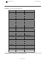
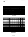
HYTEC ELECTRONICS Ltd
HEAD OFFICE: 5 CRADOCK ROAD, READING, BERKS. RG2 0JT, UK
Telephone: +44 (0) 118 9757770
Fax: +44 (0)118 9757566
E-mail: [email protected]
VICB8003 VME 64x
INDUSTRY PACK
CARRIER BOARD
WITH SHARC DSP PROCESSOR.
USERS MANUAL
PCB Issue 3
Xilinx Version 8003V603
Document Nos.: 8003/UTM/A/x/3.0
Date: 26/11/2004
Author: PJM
Hytec Electronics Ltd
8003/UTM/A/2/3.0
CONTENTS
1.
PRODUCT DESCRIPTION...............................................................................................................................3
1.1 KEY FEATURES ..................................................................................................................................................4
2.
USE OF THE VME DATA BUS AND MEMORY ACCESS..........................................................................5
2.1 VME ADDRESSING ............................................................................................................................................5
2.1.1 Short Addressing (A16 AM29h and 2Dh).................................................................................................5
ADDRESS MODIFIERS...................................................................................................................................................6
2.1.2 Standard Addressing (A24 AM39h and 3Dh)...........................................................................................6
2.1.3 Carrier board Configuration ROM (A24 AM2Fh)..................................................................................6
2.2 IP MEMORY ACCESS ..........................................................................................................................................6
2.2.1 IP Memory Size.........................................................................................................................................6
2.2.2 Carrier Board Memory Map ....................................................................................................................7
ADDRESS MODIFIERS ..................................................................................................................................................7
3.
ON BOARD FEATURES ...................................................................................................................................7
3.1 IP STATUS REGISTER (READ ONLY) ..................................................................................................................7
3.2 MEMORY OFFSET (READ/WRITE)......................................................................................................................7
3.3 CONTROL & STATUS REGISTER CARRIER BOARD (CSR CB) .............................................................................8
3.4 IP INTERRUPT SELECT REGISTER (READ/WRITE) ..............................................................................................8
3.5 VME SYSTEM AND BOARD RESETS ...................................................................................................................8
3.5.1 A VME system reset will clear the following registers:............................................................................8
3.5.2 A board reset generated from the CSR CB bit 0 will clear the following registers: ...............................8
4.
INTERRUPT SETTINGS...................................................................................................................................9
5.
VME64X KEYING AND ALIGNMENT PINS ................................................................................................9
6.
SHARC PROCESSOR AND ASSOCIATED DEVICES ............................................................................ 10
6.1 Configurations available
6.2 SHARC Control Registers
6.2.1 IP Status Register
6.2.2 Memory Offset Register
6.2.3 Control and Status Register SHARC (CSR_SH)
6.2.4 IP Interrupt Select Register
6.3 SHARC Memory Addressing
6.4 Operating Principles
6.5 Connector Pin Definitions
APPENDIX A
PCB JUMPERS.............................................................................................................................16
APPENDIX B
CARRIER BOARD CONFIGURATION ROM .........................................................................17
APPENDIX C ID PROM REGISTERS (GREENSPRING FORMAT) ................................................................18
PRODUCT SPECIFICATIONS ...............................................................................................................................19
VME64X PIN ASSIGNMENTS................................................................................................................................20
Page 2 of 21
Hytec Electronics Ltd
8003/UTM/A/3/3.0
1. PRODUCT DESCRIPTION
The VICB 8003 is a 6U (double height) VME board constructed to the VME64x standard, with EMC front
panel, injector/ejector handles, guide pin and slot keying, static discharge protection, hot swap capability, blue
power up LED, geographical addressing or jumpers, 5-row P1 and P2 connectors and 5-row P0 connector. An
Analog Devices ADSP21061 or 21062 SHARC (Super Harvard Architecture) DSP processor is also fitted for
front-end processing.
The module features hot-swap capability with auto power up and host interaction. An on-board FPGA allows
full mapping of the IP board memory, I/O and ID spaces.
The VME interface supports short I/O access A16:D32:D16:D08 (EO), standard I/O access
A24:D32:D16:D08 (EO) and extended memory access A32:D32:D16:D08 (EO).
Four Industry Pack sites are available and can accept 4 single-size Industry Packs.
The carrier board supports the 8MHz IP interface.
One of VMEbus interrupt lines IRQ1 to IRQ7 can be selected and enabled by writing to an on-board register.
The Industry Pack interrupt lines INT0 and INT1 from each of the four sites can be enabled on an individual
basis and mapped to the selected VME IRQ line.
The base address of extended memory can be set by register (offset addressing) or by geographical addressing
lines. The size of the IP memory allocated to each site can be set to 1MB, 2MB, 4MB or 8MB per site through
a control register.
Four front panel mounted LED’s flash to visually confirm completed IP access cycles to individual slots.
There is a TTL input on the front panel that allows connection to any or all of the IP card Strobe lines through
jumpers. The signal is routed through a reserved pin on the IP logic connector to allow overall control to be
applied to IP boards in data acquisition systems.
The carrier board has some thickened I/O tracks to allow the IP boards to be powered externally to give full
isolation.
All I/O is via the VME backplane P0 and P2 connectors as specified in the VME64 extensions specification.
The signals connect to the industry pack sites according to the VME64x Greenspring pinout for IP module
carriers.
Hytec has a number of rear-mounted transition cards with high-density 50-way [SCSI2] connectors, which can
cater for all 200 IP I/O signals and provide any necessary signal conditioning.
Page 3 of 21
Hytec Electronics Ltd
8003/UTM/A/4/3.0
1.1 Key Features
•
VME64 extensions / Industry Pack Carrier Board
•
VME64x rear panel I/O
•
ADPS21061 or 21062 SHARC DSP microprocessor with Flash boot EPROM and optional RAM memory
and front panel serial or LVDS link ports.
•
Full EMC shielding and insertion/extraction handles
•
Fully Hot-Swap capable with auto power-up and host interaction
•
6U (double height) VME base card
•
User selectable VME interrupt level
•
Geographical addressing
•
Front panel TTL input to IP cards via Strobe lines
•
Thickened I/O lines to allow external power supplies to IPs
•
VME 64x Configuration ROM
•
On-board clock generation
•
VME64x guide pin and slot keying
•
3.3V supply to P2 connector
•
5V supply to P2 connector
Page 4 of 21
Hytec Electronics Ltd
8003/UTM/A/5/3.0
2. USE OF THE VME DATA BUS AND MEMORY ACCESS
2.1 VME Addressing
The module uses A16/D32/D16/D08 (EO) (Even and Odd byte) or A24/D32/D16/D08 (EO) for accesses to
the IP I/O, IP ID and Carrier board Configuration Registers.
The base address of these areas is determined either by PCB jumper settings (J6 to J10) or by VME64x
geographical addressing lines GA0 to GA4.
The PCB jumpers on issue 2 boards should be used only where geographical addressing is not available and
will override the GA lines so they should not be fitted in a GA crate. Later issue 3 PCBs have a different
jumper arrangement where either jumpers or GA lines set the base address. (see appendix A)
Address
I/O Base+
Offset
0x0000
I/O Base+
0x0080
I/O Base+
0x0100
I/O Base+
0x0180
I/O Base+
0x0200
I/O Base+
0x0280
I/O Base+
0x0300
I/O Base+
0x0380
I/O Base+
0x0400
I/O Base +
0x0420
I/O Base +
0x0440
I/O Base+
0x0480
I/O Base+
0x0600
Range
Assignment
0x0000
IP A I/O Space
0x007E
0x0080
IP A ID Space
0x00FE
0x0100
IP B I/O Space
0x017E
0x0180
IP B ID Space
0x01FE
0x0200
IP C I/O Space
0x027E
0x0280
IP C ID Space
0x02FE
0x0300
IP D I/O Space
0x037E
0x0380
IP D ID Space
0x03FE
0x0400
Carrier on board registers
0x041E
0x0420
SHARC Control Registers
0x043E
0x0440
Dual-Ported SRAM accessible
0x047E
from VME and SHARC
0x0480
Green Springs Type ID
0x04FF
0x0600
VME64x configuration ROM
0x07FF
(See appendix B)
8003 A16 and A24 address Map
Size
128 Bytes
128 Bytes
128 Bytes
128 Bytes
128 Bytes
128 Bytes
128 Bytes
128 Bytes
32 Bytes
32 Bytes
64 Bytes
128 Bytes
512 Bytes
2.1.1 Short Addressing (A16 AM29h and 2Dh)
In Short address mode the geographical addressing lines equate to the address lines GA0 =A11 to GA4=A15
and the jumper address setting J6=A11 to J10=A15.
A11 - A15 is the module address determined by the setting of the relevant PCB jumpers or geographical
address lines
Address modifiers
IP I/O, IP ID and Carrier board Configuration Registers:
AM29 Short (A16) non-privileged.
AM2D Short (A16) supervisory.
Page 5 of 21
Hytec Electronics Ltd
8003/UTM/A/6/3.0
2.1.2 Standard Addressing (A24 AM39h and 3Dh)
The A24 base address is determined either by PCB jumper settings J6=A19 to J10=A23 or by geographical
addressing lines GA0 =A19 to GA4=A23.
IP I/O, IP ID and Carrier board Configuration Registers:
AM39 Standard (A24) non-privileged.
AM3D Standard (A24) supervisory.
2.1.3 Carrier board Configuration ROM (A24 AM2Fh)
See appendix B for the contents of the configuration ROM.
Address modifiers
AM2F Configuration ROM/Control & Status Registers. Address selection as above.
2.2 IP Memory Access
The module uses A32/D16/D08 (EO) (Even and Odd byte) for accesses to the IP memory.
The base address of the memory can be set by either the Geographical address lines/jumpers or by using the
Memory Offset Register. Writing a ‘1’ to bit 6 of the CSR CB register (base + 0x0408h) selects the Memory
Offset Register to set the base address.
MEM MODE (bit 6 CSRCB)
0
1
Memory Addressing Mode
Geographical address lines
Memory Offset register
Bit 6 CSR CB setting the memory address mode
Using the Memory Offset Register allows address lines A22 to A31 to be used to set the base address.
Geographical addressing uses the lines GA0=A22 to GA4=A26 – see table below.
2.2.1 IP Memory Size
Some controllers have a limited memory range so to take account of this when using geographical addressing
the memory size allocated to each IP card can be controlled: CSR CB
IPMS1
IPMS0
(bit 8)
(bit 7)
0
0
0
1
1
0
1
1
IP Memory Size
1MB
2MB
4MB
8MB
Address Lines
Geographical
Memory Offset
Addressing
Register
A22-A26 **
A22-A31
A23-A26 **
A23-A31
N/A
A24-A31
A27-A31
A25-A31
Here the GA address is shifted up one. This only allows 16 slots to be used
with geographical Addressing
NOTE ** Upper address lines A27-A31 inclusive MUST all be zero in this mode.
Page 6 of 21
Hytec Electronics Ltd
8003/UTM/A/7/3.0
2.2.2 Carrier Board Memory Map
Memory Range
Address
1MB
2MB
4MB
Memory Base + 0x000000
0x000000
0x000000
0x0FFFFE
0x1FFFFE 0x3FFFFE
Memory Base + 0x100000
0x200000
0x400000
0x1FFFFE
0x3FFFFE 0x7FFFFE
Memory Base + 0x200000
0x400000
0x800000
0x2FFFFE
0x5FFFFE 0xBFFFFE
Memory Base + 0x300000
0x600000
0xC00000
0x3FFFFE
0x7FFFFE 0xFFFFFE
Address Modifiers
Memory:
Memory Assignment
8MB
0x000000
0x7FFFFE
0x800000
0XFFFFFE
0x1000000
0x17FFFFE
0x1800000
0x1FFFFFE
IP A
IP B
IP C
IP D
AM09 or AM0D (extended non-privileged or supervisory)
3. ON BOARD FEATURES
The configuration and control of the 8003 module is achieved by the following registers:
Base
Base +
Base +
Base +
Base +
Offset
0x400
0x404
0x408
0x40C
3.1
IP Status Register (Read Only)
Address:
D15
Register
Description
IP Status
Allows state of IP INT and Error flags to be monitored
Memory Offset
Sets base address of IP memory areas
Control & Status Register CB Set up of VME part of 8003
IP Interrupt Select
Selects IP interrupts to be mapped to VME IRQ
8003 On-Board Registers
D14
Read = Base + 0x0400
D13
D12
IP
TIME
OUT
D11
ERR
D
D10
ERR
C
D09
ERR
B
D08
ERR
A
D07
INT
REQ
D1
D06
INT
REQ
C1
D05
INT
REQ
B1
D04
INT
REQ
A1
D03
INT
REQ
D0
D02
INT
REQ
C0
D01
INT
REQ
B0
D00
INT
REQ
A0
Two interrupt status and one error status bits for each of IP sites A – D plus the SHARC IP Timeout flag bit
(see section 6.2.1).
3.2 Memory Offset (Read/Write)
Address: Read = Base + 0x0404, Write = Base + 0x0404
D15
A31
D14
A30
D13
A29
D12
A28
D11
A27
D10
A26
D09
A25
D08
A24
D07
A23
D06
A22
D05
x
‘x’ = don’t care
Page 7 of 21
D04
x
D03
x
D02
x
D01
x
D00
x
Hytec Electronics Ltd
8003/UTM/A/8/3.0
3.3 Control & Status Register Carrier Board (CSR CB)
Control (Write)
Address: Base + 0x0408
D15
D14
D13
D12
D11
D10
D09
D08
D07
NU
NU
NU
NU
NU
NU
NU
IP
MS1
IP BADD IPCLK INTSEL INTSEL INTSEL INTEN Rst
MS0 SEL SEL
2
1
0
D06
D05
D04
D03
D02
D01
D00
D10
NU
D09 D08 D07 D06
D05
D04
D03
D02
D01
D00
NU IPMS IPMS BADD IPCLK INTSEL INTSEL INTSEL INTEN Rst
1
0
SEL SEL
2
1
0
Status
(Read)
Address: Base + 0x0408
D15
NU
D14
NU
Rst
INTEN
INTSEL0
INTSEL1
INTSEL2
IPCLKSEL
BADDSEL
IP MS0
IP MS1
D13
NU
D12
NU
D11
NU
Clears status register to zero when written as a ‘1’.
Enable interrupt from carrier board to VMEbus backplane.
Select VME interrupt level.
Select VME interrupt level. (See section 4).
Select VME interrupt level.
Select 8MHz IP clock =0 or 32MHz clock =1.
Select memory base address to be defined by geographical address lines=0 or by Memory
offset register=1.
Set IP memory size.
Set IP memory size. (See section 2.2)
3.4 IP Interrupt Select Register (Read/Write)
Address: Base + 0x040C
D15
NU
D14
NU
D13
NU
D12
NU
D11
NU
D10
NU
D09
NU
D08
NU
D07
D06
D05
D04
D03
D02
D01
D00
IPINT IPINT IPINT IPINT IPINT IPINT IPINT IPINT
D0
C0
D1
C1
B1
A1
B0
A0
This selects which IP interrupt lines will be enabled.
‘1’ = corresponding IP card interrupt enabled.
3.5 VME System and Board Resets
3.5.1 A VME system reset will clear the following registers:
•
•
•
CSR CB
Memory Offset Register
IP Interrupt Select register
3.5.2 A board reset generated from the CSR CB bit 0 will clear the following registers:
•
•
CSR CB
IP Interrupt Select register
Page 8 of 21
Hytec Electronics Ltd
8003/UTM/A/9/3.0
4. INTERRUPT SETTINGS
The interrupt level generated by the carrier board is set using the CSR CB register INTSEL0 (bit 2), INTSEL1
(bit 3), and INTSEL2 (bit 4).
Interrupt Level
None
IRQ 1
IRQ 2
IRQ 3
IRQ 4
IRQ 5
IRQ 6
IRQ 7
INTSEL 2 INTSEL 1 INTSEL 0
0
0
0
0
0
1
0
1
0
0
1
1
1
0
0
1
0
1
1
1
0
1
1
1
VME Interrupt Level Select
The IP Interrupt Select register allows the user to enable only the IP interrupts required and mask off the rest.
To select an IP interrupt write a ‘1’ to the appropriate bit of the register see section 3.4 above.
The interrupt vector is held on the individual IP cards.
To enable VME interrupts from the carrier board to the VMEbus backplane set bit 1 of the CSR CB to ‘1’.
Writing a ‘0’ to this register disables the interrupts.
The VME interrupt is cleared when it is acknowledged [ROAK protocol].
The IP interrupts are prioritised in the 8003 where IP A has the highest and IP D the lowest.
Each IP card can be loaded with a separate IP vector and when an interrupt occurs the controller will be given the
interrupt vector of the highest priority IP card currently asserting either of its interrupt lines.
If all four cards interrupt at the same time then IP A will be serviced first then IP B then IP C and finally IP D.
Reading the IP Status register of the 8003 at base + 0x0400 (READ ONLY) shows which IP cards have interrupts
pending.
5. VME64x KEYING AND ALIGNMENT PINS
The keying mechanism provides for three key holes on top and three keying holes on the bottom of each board
and subrack slot. Each key hole can be keyed with a “No Key” or a keying peg in one of four positions. With
three key holes top and bottom the scheme provides a total of 15,625 keying combinations.
Page 9 of 21
Hytec Electronics Ltd
6.
8003/UTM/A/10/3.0
SHARC PROCESSOR AND ASSOCIATED DEVICES
6.1 Configurations available
The 8003 board is available in a number of versions with different processors and peripherals as follows:
Model Number Processor
8003.0
8003.1
8003.2
Additional features
ADSP21061
ADSP21062
ADSP21061
None
None
Second Flash EPROM, 256K x 32 SRAM, PC16550 RS232 serial port
and two SHARC serial links on front-panel micro-D connectors.
ADSP21062
Six front-panel LVDS SHARC links on micro-D connectors.
8003.3
All units are fitted with one 1M x 8 flash EPROM boot device. This flash EPROM plus the processor’s
internal RAM and the second flash EPROM and external RAM if fitted, are all accessible from VME on a
write/read basis unless J22, the write protect jumper, is fitted. Two jumpers, J13 and J14, are used to select the
boot mode of the processor as follows:
J13
OUT
OUT
IN
IN
J14
OUT
IN
OUT
IN
Mode selected
HOST-controlled mode, boot from Host (host writes program directly into SHARC).
HOST-controlled mode, boot from Link Port.
Stand-Alone mode, boot from Flash 0. (default)
Stand-Alone mode, boot from Flash 1. (PC16550 Remote serial connect).
6.2 SHARC Control Registers
The ADSP21061/2 has its own set of registers in the Xilinx through which its operation is controlled either by
VME or the 21061/2. The set is positioned as shown in the table in Section 2.1 and comprises the following:
Base
Base +
Base +
Base +
Base +
Offset
0x420
0x424
0x428
0x42C
6.2.1
IP Status Register (R/W)
Address:
D15
Register
Description
IP Status
Allows state of IP INT and Error flags to be monitored
SHARC Memory Offset
Sets base address of SHARC memory areas in VME A32
Control & Status Register SH Set up of SHARC part of 8003
IP Interrupt Select
Selects IP interrupts to be mapped to SHARC IRQ
8003 SHARC Registers
D14
Read = Base + 0x0420
D13
D12
D11
SHARC ERR
IP
D
ERROR
D10
ERR
C
D09
ERR
B
D08
ERR
A
D07
INT
REQ
D1
D06
INT
REQ
C1
D05
INT
REQ
B1
D04
INT
REQ
A1
D03
INT
REQ
D0
D02
INT
REQ
C0
D01
INT
REQ
B0
D00
INT
REQ
A0
Two interrupt status and one error status bits for each of IP sites A – D. Plus a flag bit, bit 12, indicating a
failure when the SHARC attempted an IP access. Any write to offset 0x420 clears this bit.
Page 10 of 21
Hytec Electronics Ltd
8003/UTM/A/11/3.0
6.2.2 Memory Offset (Read/Write)
Address: Read = Base + 0x0424, Write = Base + 0x0424
D15
A31
D14
A30
D13
A29
D12
A28
D11
A27
D10
A26
D09
A25
D08
A24
D07
A23
D06
x
D05
x
D04
x
D03
x
D02
x
D01
x
D00
x
‘x’ = don’t care
6.2.3 Control & Status Register SHARC (CSR SH)
Address: Base + 0x0428
D15 D14 D13 D12 D11
FLAG FLAG FLAG FLAG OE3
2
1
0
F2/3
D10 D09 D08 D07 D06
OE- SYSR IPMS IPMS X
F0/1 ST
1
0
D05 D04 D03 D02
J22 IRQ1 IRQ0 J14
D01
J13
D00
RST
RST: Reset the SHARC processor (pulse on write ‘1’) reads ‘1’ for SHARC RUN enable.
J13/14 State of start-up jumpers, read only (RO): jumper OUT = ‘1’.
IRQ0 ‘1’ = map selected IP interrupts to SHARC IRQ0. (R/W)
IRQ1 ‘1’ = map selected IP interrupts to SHARC IRQ1. (R/W)
[Select only one of these!].
J22
State of the write protect jumper, read only (RO): jumper OUT = ‘1’ = Write Enabled.
IPMS0, 1 Reflects state of IP memory size selection from CSRCB. (RO).
SYSRST ‘1’ = Permit VME SYSRST to reset SHARC processor. (R/W).
OE-F0/1 Output enable for Flag0 and Flag1 outputs.
OE-F2/3 Output enable for Flag2 and Flag3 outputs.
Flag0 Writeable bit which, if enabled, will drive the SHARC Flag0 pin. Reads actual state.
Flag1 Writeable bit which, if enabled, will drive the SHARC Flag1 pin. Reads actual state.
Flag2 Writeable bit which, if enabled, will drive the SHARC Flag2 pin. Reads actual state.
Flag3 Writeable bit which, if enabled, will drive the SHARC Flag3 pin. Reads actual state.
6.2.4 IP Interrupt Select Register (Read/Write)
Address: Base + 0x042C
D15
NU
D14
NU
D13
D12
NU SHARC
IP
ERROR
D11
NU
D10
NU
D09
NU
D08
NU
D07
D06
D05
D04
D03
D02
D01
D00
IPINT IPINT IPINT IPINT IPINT IPINT IPINT IPINT
D0
C0
D1
C1
B1
A1
B0
A0
This selects which IP interrupt lines will be mapped to the SHARC IRQ line selected in CSR SH. Note that it
would be incorrect to map an IP interrupt to both VME and SHARC. It also allows the SHARC IP ERROR bit
to be mapped to the SHARC IRQ.
‘1’ = corresponding IP card interrupt enabled.
6.3 SHARC Memory Addressing
The internal RAM of the SHARC processor and its peripherals, the flash EPROM(s) and external RAM are all
accessible from VME through offset addressing. The offset is specified in the register described in section
6.2.2.
Page 11 of 21
Hytec Electronics Ltd
8003/UTM/A/12/3.0
Note also that the way that the SHARC processor addresses memory is quite different from that used in VME.
That is, whatever the size of the addressed object, the address increment is always 1. Thus consecutive bytes
of the flash EPROM as seen from the SHARC are at addresses 00000000, 00000001 and 00000002 and
consecutive 32-bit data words in its memory or the external data memory are likewise addressed at 0xx00000,
0xx00001 and 0xx00002, where ‘xx’ represents upper address bits to select the appropriate area of memory.
In order to connect this strange arrangement to VME, the least significant address line of VME, namely A1,
has been connected to the least significant SHARC address line. Thus consecutive bytes in a flash EPROM
will appear as lower (D00-D07) bits in consecutive words of VME space. When composing write commands
to the flash, it should be remembered that in order to produce a particular EPROM address, double that value
needs to be placed on the VME address lines.
[i.e. shift the address up one bit].
When consecutive 32-bit words of SHARC internal RAM or external RAM (if fitted) are addressed from
VME in D32 mode (LWORD asserted), the VME address is further shifted down one bit in order to map these
areas correctly and make them accessible to the host – see the address map below. If LWORD is not asserted
(i.e.D16 mode) this address shift does not occur making SHARC internal memory ‘Short Word Addressing’
possible.
6.3.1 SHARC VME Memory Addressing Map.
Offset from Register SHARC
-set Base Address
Address
Contents
000000 -0003FC
000000-0000FF SHARC IOP Registers – D32 only
080000-08FFFC
020000-023FFF SHARC Internal RAM Block 0 - Normal Word Addressing - D32
090000-09FFFC
024000-027FFF SHARC Internal RAM Block 1 - Normal Word Addressing - D32
[32-bit long words on long word boundaries or 16-bit lower/upper words on word boundaries if SHARC Short
Word Addressing is selected by NOT asserting LWORD – D16].
For example, D32 write/read 0x12345678 at offset 0x090000, then D16 read 0x5678 at offset 0x090000 and
0x1234 at offset 0x090002.
200000-3FFFFE
MS0 or BMS
Flash EPROM 0 [D0-7 bytes on word boundaries]
400000 -5FFFFE
MS0 + 0x100000 Flash EPROM 1 (if fitted) [D0-7 bytes on word boundaries]
600000 -6FFFFC
MS2
SHARC external RAM (if fitted) [256K x 32-bit long words
on long-word boundaries: D32 only]
6.3.2
SHARC Address Map
The way that the SHARC processor addresses external devices is on the basis of banks. Each bank has a chip
select line associated with it and a register, which defines how cycles are completed. The four select lines are
connected as follows:
MS0 or BMS (Boot memory select) connects to flash memory 0 or 1 (chosen by the Xilinx).
MS1 connects to the PC16550 UART device, if fitted.
MS2 connects to the external RAM
MS3 connects to the Xilinx for access to internal registers and the IP cards.
All except MS3 should have their cycles completed internally by the wait state machine. The default value of
6 internal clocks (of the 32MHz master clock) is OK for all these devices. Cycles to the Xilinx (and to the IP
cards through the Xilinx) should be terminated externally by ACK after an internal wait of 6 clocks.
The actual access times of the external devices, if fitted, are as follows and the user may trim the wait state
machine to these timings if desired:
Flash EPROM:90 nanoseconds.
SRAM:
20 nanoseconds
Page 12 of 21
Hytec Electronics Ltd
8003/UTM/A/13/3.0
PC16550 UART: 150 nanoseconds approx. (use 6 wait states).
SHARC Address Map:
Address Range
Contents
00000000-0007FFFF
00080000-003FFFFF
00400000-004FFFFF
00500000-005FFFFF
00600000-00BFFFFF
00C00000-013FFFFF
01400000-014FFFFF
01500000-01BFFFFF
01C00000-01C007FF
02000000-020FFFFF
02100000-021FFFFF
02200000-022FFFFF
02300000-023FFFFF
SHARC Internal RAM
SHARC multi-processor space (not used).
Flash EPROM 0.
Flash EPROM 1.
Aliases of Flash EPROM’s 0 and 1.
PC16550 UART Device – only a very small part used!
256K X 32-bits External RAM (if fitted).
Aliases of external RAM.
IP I/O and ID access plus Xilinx registers (as VME A16 map).
IP ‘A’ Memory access (1M 16-bit words).
IP ‘B’ Memory access.
IP ‘C’ Memory access.
IP ‘D’ Memory access.
Thus each of MS0, 1, 2 and 3 MUST to be set up as 8M blocks.
The Xilinx provides ACK termination for all accesses by MS3, whether the SHARC addresses internal
registers, configuration data, dual-ported RAM or IP cards. It also provides termination even if the addressed
device is not present (that is an absent or faulty IP card).
6.4 Operating Principles
The normal procedure for operating the SHARC processor on this card is to develop a program for it, load it
into the flash EPROM and then let it run. Some applications may require the program to be downloaded to the
card over a serial line and then programmed into the flash by the SHARC processor. This requires a
‘secondary’ boot program, which is held in the optional second flash device as a ‘low level boot program’.
Care should be exercised when down-loading a program to the SHARC since in certain modes it is looking
constantly for the appearance of valid code in certain locations, for example in host-booted mode. For this
reason it is recommended that the first word of code be written last.
Internally, the 8003 has a shared address and data bus. There are two possible masters of this bus – the
SHARC processor and the VME port (through the Xilinx). By default, the SHARC is bus master and the VME
port requests use of the bus when it decodes a valid address and modifier. It does this by asserting host bus
request (HBR) and receiving host bus grant (HBG). The time taken to achieve this will depend on what the
SHARC is doing when the request arrives but there should be no more than a 1 microsecond delay. The
SHARC experiences a similar ‘interruption’ if the VME port uses the bus. In order to be able to examine
VME addresses while the SHARC is in control of the bus, the address lines are separated by a set of buffers.
When the SHARC wishes to address the Xilinx-connected areas (that is the IP cards and Xilinx internal areas)
or when the VME port wishes to access SHARC memory areas, the buffers are used to connect the address
lines together. If the SHARC does access Xilinx-connected areas using MS3, this signal is used to inhibit the
VME address-decoding scheme and turn off any VME buffers which would contend with the SHARC cycle.
Page 13 of 21
Hytec Electronics Ltd
8003/UTM/A/14/3.0
It is important to bear in mind that if the SHARC processor attempts to address an area of memory which does
not physically exist (that is outside the ranges shown in the above address map) then cycle termination will
not take place and the processor will enter a ‘hung’ state. In the unlikely event that this should happen then a
working program MUST replace the program that caused it to happen. The difficulty is that if the processor
enters the ‘hung’ state then the usual mechanism for changing the program, writing to the flash from VME,
will not work because it relies on the SHARC granting the bus to the VME port, which at this stage it is
unable to do. Nor can the SHARC rectify the problem itself since it is unable to communicate with anything.
The only exit from this ‘deadly embrace’ is to power the board off and select a different start-up mode such as
booting from a link port. The processor will not find a program to run and enter a dormant state in which it is
possible for you to re-program the flash with working code.
6.5 Connector Pin Definitions
As described in Section 6.1, some of the variants of this board have front-panel connectors. The details of
these are as follows:
8003.2:
CON1 ‘RS232’ 9-way Micro-D Connector for the RS232 signals from the PC16550DV UART device.
Pins 1, 2, 3, 4, 5:
Pin 6:
Pin 7:
Pin 8:
Pin 9:
GND
Clear to Send (CTS) Input
Serial Data Input
Serial Data Output
Request to Send (RTS) Output.
Note: The 16550 can be programmed to ignore the state of the CTS input.
Connector part number: ITT Cannon MDSM-9PE-Z10-VR1; Electrospeed 17-0628K. Mating connector ITT
Cannon MDSM-9SC-Z11-VS1; Electrospeed 17-0631F with crimp contacts MDS-S-H; Electrospeed 170634B..
CON3 ‘SSP0’ 15-way Micro-D Connector for the TTL signals from the SHARC Synchronous Serial Port 0.
Pin 1:
Pin 2:
Pin 3:
Pin 4:
Pin 5:
Pin 6:
Pin 7:
Pins 8-15
GND
Transmit Data Output (DT0)
Receive Data Input (DR0)
Transmit Clock Output (TCLK0)
Receive Clock Input (RCLK0)
Transmit Frame Sync. Output (TFS0)
Receive Frame Sync. Input (RFS0)
No Connect.
Connector part number: ITT Cannon MDSM-15PE-Z10-VR1; Electrospeed 17-0629E. Mating connector ITT
Cannon MDSM-15SC-Z11-VS1; Electrospeed 17-0632A with crimp contacts MDS-S-H; Electrospeed 170634B.
Page 14 of 21
Hytec Electronics Ltd
8003/UTM/A/15/3.0
CON4 ‘SSP1’ 15-way Micro-D Connector for the TTL signals from the SHARC Synchronous Serial Port 1.
Pin 1:
Pin 2:
Pin 3:
Pin 4:
Pin 5:
Pin 6:
Pin 7:
Pins 8-15
GND
Transmit Data Output (DT1)
Receive Data Input (DR1)
Transmit Clock Output (TCLK1)
Receive Clock Input (RCLK1)
Transmit Frame Sync. Output (TFS1)
Receive Frame Sync. Input (RFS1)
No Connect.
8003.3:
CON 2, CON3, CON4 Double-stacked 2 x 15-way Micro-D Connectors for the LVDS signals from SHARC
Link Ports 0 and 1, 2 and 3 and 4 and 5 respectively.
Each of the six connector parts has the same pinout as follows:Pin 1:
Pin 9:
Pin 2:
Pin 10:
Pin 3:
Pin 11:
Pin 4:
Pin 12:
Pin 5:
Pin 13:
Pin 6:
Pin 14:
Pin 7:
Pin 8:
Pin 15:
GND
Link Clock (-)
Link Clock (+)
Link Acknowledge (-)
Link Acknowledge (+)
Link Data Bit 2 (-)
Link Data Bit 2 (+)
Link Data Bit 3 (-)
Link Data Bit 3 (+)
Link Data Bit 0 (-)
Link Data Bit 0 (+)
Link Data Bit 1 (-)
Link Data Bit 1 (+)
VCC through a zero ohm resistor.
No Connect.
Connector part number: ITT Cannon MDSM-30PE-Z10-VR22; Electrospeed 17-54859D. Mating connectors
(2 off required for each) ITT Cannon MDSM-15SC-Z11-VS1; Electrospeed 17-0632A with crimp contacts
MDS-S-H; Electrospeed 17-0634B.
Page 15 of 21
Hytec Electronics Ltd
APPENDIX A
8003/UTM/A/16/3.0
PCB JUMPERS
Hytec 8003 SHARC IP Carrier Board
J1
J2
J3
J4
J5
J6 – J10
J6
J7
J8
J9
J10
J11
J12
J13, J14
J15
J16
J19
J17
J20
J18
J21
J22
Connects the common strobe line from the Xilinx to Industry Pack C Logic Connector pin 46.
Must be IN Factory set.
Connects the common strobe line from the Xilinx to Industry Pack A Logic Connector pin 46.
Supplies switched and fused +5V to pins P2 A32 and P2 C32 (Delivered Not selected).
Connects the common strobe line from the Xilinx to Industry Pack B Logic Connector pin 46.
Base address setting: Used to select either Geographical Addressing or jumper setting.
Make according to required A11-A15 base address as follows:
Fitted AUTO
A11 must match GA0
A12 must match GA1
A13 must match GA2
A14 must match GA3
A15 must match GA4
Fitted MANUAL
A11 must be ‘0’
A12 must be ‘0’
A13 must be ‘0’
A14 must be ‘0’
A15 must be ‘0’
Not fitted
A11 must be ‘1’
A12 must be ‘1’
A13 must be ‘1’
A14 must be ‘1’
A15 must be ‘1’
Connects the common strobe line from the Xilinx to Industry Pack D Logic Connector pin 46.
Must be IN Factory set.
Set the SHARC processor start-up mode. See section 6.
SHARC JTAG test disable – should be fitted unless using the JTAG test port.
LVDS SHARC Link Port 0 RX/TX select – link centre pin to either TX or RX.
LVDS SHARC Link Port 1 RX/TX select – link centre pin to either TX or RX.
LVDS SHARC Link Port 2 RX/TX select – link centre pin to either TX or RX.
LVDS SHARC Link Port 3 RX/TX select – link centre pin to either TX or RX.
LVDS SHARC Link Port 4 RX/TX select – link centre pin to either TX or RX.
LVDS SHARC Link Port 5 RX/TX select – link centre pin to either TX or RX.
Write protects SHARC memory areas from VME – IN = write protect.
Note: The reference to the ‘Common Strobe Line’ refers to the front panel Inhibit signal which is passed
through by the Xilinx unprocessed, thus asserting the Inhibit input low will drive all connected IP logic
connector pins 46 low.
Page 16 of 21
Hytec Electronics Ltd
APPENDIX B
8003/UTM/A/17/3.0
Carrier Board Configuration ROM
Address Offset
0x03
0x07
0x0B
Value
C1
00
02
00
0x0F
Definition
Check Sum
Length of ID ROM MSB
Length of ID ROM
Length of ID ROM LSB
Configuration ROM data access width
0x83
CSR data access width
0x83
CSR space Specification ID
VME64x-1997
0x02
Identify a Valid CR
‘C’
0x43
‘R’
0x52
Manufacturer’s ID
0x00
0x13
0x17
0x1B
0x1F
0x23
0x27
0x2B
0x2F
0x80
0x03
Board ID
0x33
0x37
0x3B
0x3F
0x80
0x03
0x00
0x00
0x43
0x47
0x4B
0x4F
0x03
0x06
0x00
0x03
Board build 0,1, 2 or 3.
Revision ID
PCB issue
Xilinx version
Xilinx revision nos
Xilinx revision nos
ASCII string null terminated or 0x000000
0x53
0x57
0x5B
0x00
0x00
0x00
Reserved for future use
0x5F to 0x7B
Program ID code
0x7F
0x01
No program, ID ROM only
Start of user defined area
0x80
Board Serial Number
0xCB, 0xCF, 0xD3
0xD7, 0xDB, 0xDF
0x
0x
BEG_SN MSB
END_SN LSB
0x123.. 0x13F
0x2200220000002200
AM code mask
AM codes 3D, 39, 2D, 29, 0D,
09
Reading the Configuration ROM using A16 (AM29h and AM2Dh) or A24 (AM39h and AM3Dh) the address
is VME base address + 0x0600h, the Configuration ROM offset.
Page 17 of 21
Hytec Electronics Ltd
8003/UTM/A/18/3.0
APPENDIX C ID PROM Registers (GreenSpring Format)
Address Offset
0x481
0x483
0x485
0x487
0x489
0x48B
0x48D
0x48F
0x491
0x493
0x495
0x487
Value
0x49
0x50
0x41
0x43
0x80
0x83
0x0x
0x00
0x00
0x00
0x0C
Definition
ASCII “I”
ASCII “P”
ASCII “A”
ASCII “C”
Manufacturer’s ID
Model Number
Revision
Reserved
Driver ID, low byte
Driver ID, high byte
No of bytes used
CRC
Page 18 of 21
Hytec Electronics Ltd
8003/UTM/A/19/3.0
PRODUCT SPECIFICATIONS
Power Requirements
+5V @ 600mA typical
+12V @ 30mA
-12V @ 30mA
+3.3V @ approx 10mA
Additional power maybe consumed by Industry Packs.
Operating Temperature Range
0 to +45 deg Celsius ambient.
Mechanical
6U single width VME module with access to 5 row P0, P1 and P2 connectors.
IP Memory Mapping
VME Access A32:D16:D8 (EO) AM Codes: 09h and 0Dh.
IP I/O Mapping
VME Access A16:D16:D8 (EO) AM Codes: 29h and 2Dh.
VME Access A24:D16:D8 (EO) AM Codes: 39h and 3Dh.
Front Panel Indicators and Inputs
‘VME’
LED (green)
‘Not Configured
LED (blue)
IP ACK
4 LED’s (red)
Illuminates for a minimum of 20msecs whenever the
module is accessed via the VME bus.
Indicates the state of the VME module during hot swap
operation.
Indicate when an IP card has sent an ACK.
Front Panel Inputs
Inhibit
Single TTL. This input has a 10K pull-up resister to 5Volt supply.
Connector type: LEMO RA0302
Page 19 of 21
Hytec Electronics Ltd
8003/UTM/A/20/3.0
VME64x PIN ASSIGNMENTS
ROW A
P0.A01
P0.A02
P0.A03
P0.A04
P0.A05
P0.A06
P0.A07
P0.A08
P0.A09
P0.A10
P0.A11
P0.A12
P0.A13
P0.A14
P0.A15
P0.A16
P0.A17
P0.A18
P0.A19
SIG
IODO1
IOD06
IOD11
IOD16
IOD21
IOD26
IOD31
IOD36
IOD41
IOD46
IOC01
IOC06
IOC11
IOC16
IOC21
IOC26
IOC31
IOC36
IOC41
ROW B
P0.B01
P0.B02
P0.B03
P0.B04
P0.B05
P0.B06
P0.B07
P0.B08
P0.B09
P0.B10
P0 B11
P0.B12
P0.B13
P0.B14
P0.B15
P0.B16
P0.B17
P0.B18
P0.B19
SIG
IOD02
IOD07
IOD12
IOD17
IOD22
IOD27
IOD32
IOD37
IOD42
IOD47
IO002
IO007
IO012
IO017
IOC22
IO027
IO032
IO037
IO042
ROW C
P0.C01
P0.C02
P0.C03
P0.C04
P0.C05
P0.C06
P0.C07
P0.C08
P0.C09
P0.C10
P0.C11
P0.C12
P0.C13
P0.C14
P0.C15
P0.C16
P0.C17
P0.C18
P0.C19
SIG
IOD03
IOD08
IOD13
IOD18
IOD23
IOD28
IOD33
IOD38
IOD43
IOD48
IOC03
IOC08
IOC13
IOC18
IOC23
IOC28
IOC33
IOC38
IOC43
ROW D
P0.DO1
P0.D02
P0.D03
P0.D04
P0.D05
P0.D06
P0.D07
P0.D08
P0.D09
P0.D10
P0.D11
P0.D12
P0.D13
P0.D14
P0.D15
P0.D16
P0.D17
P0.D18
P0.D19
SIG
IOD04
IOD09
IOD14
IOD19
IOD24
IOD29
IOD34
IOD39
IOD44
IOD49
IOC04
IOC09
IOC14
IOC19
IOC24
IOC29
IOC34
IOC39
IOC44
ROW E
P0.E01
P0.E02
P0.E03
P0.E04
P0.E05
P0.E06
P0.E07
P0.E08
P0.E09
P0.E10
P0 E11
P0.E12
P0.E13
P0.E14
P0.E15
P0.E16
P0.E17
P0.E18
P0.E19
SIG
IOD05
IODlO
IOD15
IOD20
IOD25
IOD30
IOD35
IOD40
IOD45
IOD50
IOC05
IOC10
IOC15
IOC20
IOC25
IOC30
IOC35
IOC40
IOC45
ROW F
P0.F01
P0.F02
P0.F03
P0.F04
P0.F05
P0.F06
P0.F07
P0.F08
P0.F09
P0.F10
P0.F11
P0.F12
P0.F13
P0.F14
P0.F15
P0.F16
P0.F17
P0.F18
P0.F19
SIG
GND
GND
GND
GND
GND
GND
GND
GND
GND
GND
GND
GND
GND
GND
GND
GND
GND
GND
GND
P0 pin assignments
P1 ROW A
P1.A01
P1.A02
P1.A03
P1.A04
P1.A05
P1.A06
P1.A07
P1.A08
P1.A09
P1.A10
P1.A11
P1.A12
P1.A13
P1.A14
P1.A15
P1.A16
P1.A17
P1.A18
P1.A19
P1.A20
P1.A21
P1.A22
P1.A23
P1.A24
P1.A25
P1.A26
P1.A27
P1.A28
P1.A29
P1.A30
P1.A31
P1.A32
SIGNAL
D00
D01
D02
D03
D04
D05
D06
D07
GND
N/C
GND
DS1*
DS0*
WRITE
GND
DTACK*
GND
AS
GND
IACK
IACKIN*
IACKOUT
AM4
A07
A06
A05
A04
A03
A02
A0l
-12V
+5V
P1 ROW B
P1.B01
P1.B02
P1.B03
P1.B04
P1.B05
P1.B06
P1.B07
P1.B08
P1.B09
P1.B10
P1.B11
P1.B12
P1.B13
P1.B14
P1.B15
P1.B16
P1.B17
P1.B18
P1.B19
P1.B20
P1.B21
P1.B22
P1.B23
P1.B24
P1.B25
P1.B26
P1.B27
P1.B28
P1.B29
P1.B30
P1.B31
P1.B32
SIGNAL
N/C
N/C
N/C
BG0IN*
BG0OUT*
BG1IN*
BG1OUT*
BG2IN*
BG2OUT*
BG3IN*
BG3OUT*
N/C
N/C
N/C
N/C
AM0
AM1
AM2
AM3
GND
N/C
N/C
GND
IRQ7*
IRQ6*
IRQ5*
IRQ4*
IRQ3*
IRQ2*
IRQ1*
N/C
+5V
P1 ROW C
P1.C01
P1.C02
P1.C03
P1.C04
P1.C05
P1.C06
P1.C07
P1.C08
P1.C09
P1.C10
P1.C11
P1.C12
P1.C13
P1.C14
P1.C15
P1.C16
P1.C17
P1.C18
P1.C19
P1.C20
P1.C21
P1.C22
P1.C23
P1.C24
P1.C25
P1.C26
P1.C27
P1.C28
P1.C29
P1.C30
P1.C31
P1.C32
SIGNAL
D08
D09
D10
D11
D12
D13
D14
D15
GND
N/C
BERR*
RESET
LWORD*
AM5
A23
A22
A21
A20
A19
A18
A17
A16
A15
A14
A13
A12
A11
A10
A09
A08
+12V
+5V
P1 Pin Assignments
Page 20 of 21
P1 ROW D
P1.D01
P1.D02
P1.D03
P1.D04
P1.D05
P1.D06
P1.D07
P1.D08
P1.D09
P1.D10
P1.D11
P1.D12
P1.D13
P1.D14
P1.D15
P1.D16
P1.D17
P1.D18
P1.D19
P1.D20
P1.D21
P1.D22
P1.D23
P1.D24
P1.D25
P1.D26
P1.D27
P1.D28
P1.D29
P1.D30
P1.D31
P1.D32
SIGNAL
N/C
N/C
N/C
N/C
N/C
N/C
N/C
N/C
N/C
N/C
N/C
+3.3V
N/C
+3.3V
N/C
+3.3V
N/C
+3.3V
N/C
+3.3V
N/C
+3.3V
N/C
+3.3V
N/C
+3.3V
N/C
+3.3V
N/C
+3.3V
N/C
+5V
P1 ROW Z
P1.Z01
P1.Z02
P1.Z03
P1.Z04
P1.Z05
P1.Z06
P1.Z07
P1.Z08
P1.Z09
P1.Z10
P1.Z11
P1.Z12
P1.Z13
P1.Z14
P1.Z15
P1.Z16
P1.Z17
P1.Z18
P1.Z19
P1.Z20
P1.Z21
P1.Z22
P1.Z23
P1.Z24
P1.Z25
P1.Z26
P1.Z27
P1.Z28
P1.Z29
P1.Z30
P1.Z31
P1.Z32
SIGNAL
N/C
GND
N/C
GND
N/C
GND
N/C
GND
N/C
GND
N/C
GND
N/C
GND
N/C
GND
N/C
GND
N/C
GND
N/C
GND
N/C
GND
N/C
GND
N/C
GND
N/C
GND
N/C
GND
Hytec Electronics Ltd
ROWA
P2.A01
P2.A02
P2.A03
P2.A04
P2.A05
P2.A06
P2.A07
P2.A08
P2.A09
P2.A10
P2.A11
P2.A12
P2.A13
P2.A14
P2.A15
P2.A16
P2.A17
P2.A18
P2.A19
P2.A20
P2.A21
P2.A22
P2.A23
P2.A24
P2.A25
P2.A26
P2.A27
P2.A28
P2.A29
P2.A30
P2.A31
P2.A32
SIG
IOB41
IOB43
IOB45
IOB47
IOB49
IOA01
IOA03
IOA05
IOA07
IOA09
IOA11
IOA13
IOA15
IOA17
IOA19
IOA21
IOA23
IOA25
IOA27
IOA29
IOA31
IOA33
IOA35
IOA37
IOA39
IOA41
IOA43
IOA45
IOA47
IOA49
+3.3V
Out+5V
ROWB
P2.B01
P2.B02
P2.B03
P2.B04
P2.B05
P2.B06
P2.B07
P2.B08
P2.B09
P2.B10
P2.B11
P2.B12
P2.B13
P2.B14
P2.B15
P2.B16
P2.B17
P2.B18
P2.B19
P2.B20
P2.B21
P2.B22
P2.B23
P2.B24
P2.B25
P2.B26
P2.B27
P2.B28
P2.B29
P2.B30
P2.B31
P2.B32
8003/UTM/A/21/3.0
SIG
+5V
GND
N/C
A24
A25
A26
A27
A28
A29
A30
A31
GND
+5V
N/C
N/C
N/C
N/C
N/C
N/C
N/C
N/C
GND
N/C
N/C
N/C
N/C
N/C
N/C
N/C
N/C
GND
+5V
ROWC
P2.C01
P2.C02
P2.C03
P2.C04
P2.C05
P2.C06
P2.C07
P2.C08
P2.C09
P2.C10
P2.C11
P2.C12
P2.C13
P2.C14
P2.C15
P2.C16
P2.C17
P2.C18
P2.C19
P2.C20
P2.C21
P2.C22
P2.C23
P2.C24
P2.C25
P2.C26
P2.C27
P2.C28
P2.C29
P2.C30
P2.C31
P2.C32
SIG
IOB42
IOB44
IOB46
IOB48
IOB50
IOA02
IOA04
IOA06
IOA08
IOA10
IOA12
IOA14
IOA16
IOA18
IOA20
IOA22
IOA24
IOA26
IOA28
IOA30
IOA32
IOA34
IOA36
IOA38
IOA40
IOA42
IOA44
IOA46
IOA48
IOA50
+3.3V
Out+5V
ROWD
P2.D01
P2.D02
P2.D03
P2.D04
P2.D05
P2.D06
P2.D07
P2.D08
P2.D09
P2.D10
P2.D11
P2.D12
P2.D13
P2.D14
P2.D15
P2.D16
P2.D17
P2.D18
P2.D19
P2.D20
P2.D21
P2.D22
P2.D23
P2.D24
P2.D25
P2.D26
P2.D27
P2.D28
P2.D29
P2.D30
P2.D31
P2.D32
SIG
IOC47
IOC48
IOC50
IOB0l
IOB03
IOB04
IOB06
IOB07
IOB09
IOB10
IOB12
IOB13
IOB15
IOB16
IOB18
IOB19
IOB21
IOB22
IOB24
IOB25
IOB27
IOB28
IOB30
IOB31
IOB33
IOB34
IOB36
IOB37
IOB39
IOB40
N/C
+5V
ROWZ
P2.Z01
P2.Z02
P2.Z03
P2.Z04
P2.Z05
P2.Z06
P2.Z07
P2.Z08
P2.Z09
P2.Z10
P2.Z11
P2.Z12
P2.Z13
P2.Z14
P2.Z15
P2.Z16
P2.Z17
P2.Z18
P2.Z19
P2.Z20
P2.Z21
P2.Z22
P2.Z23
P2.Z24
P2.Z25
P2.Z26
P2.Z27
P2.Z28
P2.Z29
P2.Z30
P2.Z31
P2.Z32
SIG
IOC46
GND
IOC49
GND
IOB02
GND
IOB05
GND
IOB08
GND
IOB11
GND
IOB14
GND
IOB17
GND
IOB20
GND
IOB23
GND
IOB26
GND
IOB29
GND
IOB32
GND
IOB35
GND
IOB38
GND
+3.3V
GND
P2 pin assignments
Denotes pins with thickened tracks which can be used for power inputs
Note:
‘Out+5V’ is provided by the 8003 board and can be put on to the pins by fitting jumper J4.
Page 21 of 21