1
MIPS® SEAD™-3 IO Processor User’s Manual
Document Number: MD00630
Revision 01.01
September 8, 2011
MIPS Technologies, Inc.
955 East Arques Avenue
Sunnyvale, CA 94085-4521
Copyright © 2009 MIPS Technologies Inc. All rights reserved.
Contents
Section 1: Introduction........................................................................................................................... 3
Section 2: Hardware Description .......................................................................................................... 3
2.1: PIC32 / Core Logic Interface Signals .......................................................................................................... 3
2.2: IO Processor Connectors ............................................................................................................................ 4
2.2.1: J3 – Serial Connector......................................................................................................................... 5
2.2.2: J5 - GPIO Connector.......................................................................................................................... 5
2.2.3: ICD Debug Connector........................................................................................................................ 7
Section 3: IO Processor Software Interface ......................................................................................... 8
3.1: Basic Protocol.............................................................................................................................................. 8
3.2: Command Formatting.................................................................................................................................. 8
3.3: IO Processor Command Status................................................................................................................... 9
3.4: Register Write Command ............................................................................................................................ 9
3.5: Register Read Command .......................................................................................................................... 10
3.6: PIC32 System Register Read and Commands Write Sequence............................................................... 11
3.6.1: System Null Command (read or write) ............................................................................................. 11
3.6.2: System Reset Command ................................................................................................................. 12
3.6.3: Firmware Version ............................................................................................................................. 12
3.7: Interrupt Support........................................................................................................................................ 12
Section 4: PIC32 Firmware Code......................................................................................................... 13
Section 5: SEAD-3 IO Processor ICD Interface Cable ....................................................................... 19
Section 6: References .......................................................................................................................... 20
Section 7: Revision History ................................................................................................................. 20
2
MIPS® SEAD™-3 IO Processor User’s Manual, Revision 01.01
Copyright © 2009 MIPS Technologies Inc. All rights reserved.
1 Introduction
1 Introduction
The SEAD-3™ development platform takes advantage of a MIPS M4K®-based microcontroller from Microchip to
provide basic General Purpose IO (GPIO), I2C, SPI, and Analog to Digital input ports, The MicroSD card and Real
Time Clock functionality of the SEAD-3 board is also provided by the PIC32 IO Processor
The PIC32-based IO processor is connected to the main SEAD-3 board core logic via an 8-bit parallel interface port.
A simple wrapper interface protocol is used to communicate between the SEAD-3 core logic and the PIC32 IO Processor. This protocol wrapper exposes a subset of the relevant PIC32 registers into a specific area of the SEAD-3
memory map. Support for local PIC32 peripheral interrupts is also provided through a thin protocol wrapper as well.
The source code for the PIC32 IO Processor is provided to allow users to add and change functionality as needed for
their specific application. The IO Processor is fully supported and easily interfaced to Microchip’s standard development environment and inexpensive toolchain.
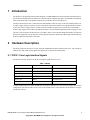
2 Hardware Description
The SEAD-3 PIC32 IO Processor is based on the PIC32MX360F512Lmicrocontroller. This device, with 512 KB of
Flash memory and 32 KB of Static RAM, has ample room for expansion of functionality.
2.1 PIC32 / Core Logic Interface Signals
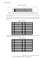
The SEAD-3 bus logic interfaces to the PIC32 using the signals shown in Table 1.
Table 1 Modes
SEAD-3 Core
PIC32
Description
PI_LOC_D7 .. PI_LOC_D0
PMD7 .. PMD0
PMP Data
PI_LOC_WE_N
PMWR
PMP Write Strobe
PI_LOC_RD_N
PMRD
PMP Read Strobe
PI_LOC_CS_N
PMPCS1
PMP Chip Select
PI_LOC_A4
PMA1
PMP Address Bit 1
PI_LOC_A3
PMA0
PMP Address Bit 0
In buffered addressable slave mode, the PMP port on the PIC32 provides a 4 x 8-bit read/write register space. In this
configuration, four discrete read or write cycles will be needed to native 32-bit data between the SEAD-3 core logic
and the PIC32 device.
MIPS® SEAD™-3 IO Processor User’s Manual, Revision 01.01
Copyright © 2009 MIPS Technologies Inc. All rights reserved.
3
2 Hardware Description
Each byte within the 4-byte read and write buffer of the PMP interface is directly addressed using the two address
lines, as shown below.
0
PMP Byte
PMA1
PMA0
0
0
0
1
0
1
2
1
0
3
1
1
Four status signals, listed below, are provided by the PIC32 microcontroller to the SEAD-3 core logic.
Signal
PIC32 Pin
PIC32_IO_CMD_RDY
RC1
PIC32_INTID0
RC2
PIC32_INTID1
RC3
PIC32_INTID2
RC4
The PIC32_IO_CMD_RDY signal is asserted high when the pending operation has been completed and a status byte
is available in the PMP interface read buffer at address 0.
PIC32_INTID (2:0) are used both to signal an interrupt and to provide the interrupt to the SEAD-3 bus logic.
The SEAD-3 bus control logic automatically takes care of the 4-byte read and write sequence to the 8-bit wide IO
Processor interface by mapping a full 32-bit wide port to memory at location 0xBF000600.
The status signals are also grouped together in one 32-bit memory-mapped location in the host processor memory
space 0xBE80060.
The status register bit formats are defined as follows:
Bit
Bit
Bit
Bit
Bit
31 -> Bit 4 : Reserved
3 : INTID3
2 : INTID2
1 : INTID1
0 : IO_CMD_RDY
The host processor register locations are summarized in the table below.
0xBF000600
32-bit IO Processor Command/Data Register
Read/Write
0xBE000060
32-bit IO Processor Status Register
Read only
All 32-bit addresses and data formatted in the protocol scheme are little-endian, regardless of the endianness of the
SEAD-3 Core CPU configuration. The SEAD-3 core logic will provide the required translation transparently when
supporting a big-endian MIPS32 host processor core.
2.2 IO Processor Connectors
The SEAD-3 IO Processor presents 3 connectors on the SEAD-3 motherboard, as described below.
4
MIPS® SEAD™-3 IO Processor User’s Manual, Revision 01.01
Copyright © 2009 MIPS Technologies Inc. All rights reserved.
2 Hardware Description
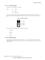
2.2.1 J3 – Serial Connector
Connector type – 3 position inline 0.1" pin header
Signals :
Pin 1
TXD out
Pin 2
RXD in
Pin 3
Signal GND
This connector presents RS232-level compatible signals and is connected to UART1 of the PIC32 IO Processor.
While generally used for additional debugging of the IO Processor firmware, this serial port is available for general
use.
Figure 1 J3 Serial Connector
Pin 1 - TXD
Pin 2 - RXD
Pin 3 - GND
The default serial communication parameters used by this serial port are:
•
115200 baud
•
8 data bits
•
1 stop bit
•
no parity
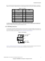
2.2.2 J5 - GPIO Connector
All general-purpose IO signals are available on J5, which is a 3 X 18 .1" center-pin header array. This connector is
located at the rear center of the SEAD-3 board. Pin 1 of all rows is on the left, with Row A located toward the center
of the circuit board.
MIPS® SEAD™-3 IO Processor User’s Manual, Revision 01.01
Copyright © 2009 MIPS Technologies Inc. All rights reserved.
5
2 Hardware Description
Figure 2 J5 Connector
C
B
A
1
18
The pin assignments are shown in the tables below. The specific PIC32 Pin signal ID is included in the Signal column
inside square brackets ‘[ ]’.
Row A consists primarily of all of the GPIO pins available from the PIC32 microcontroller. These are true generalpurpose IO pins that are configurable as outputs. Please refer to the PIC32MX360F512L device datasheet for further
information.
Table 2
J5 - Row A
Pin
Signal
Pin
Signal
1
GPI00 [RD6]
10
GPI09 [RG1]
2
GPI01 [RD7]
11
GPI010 [RG2]
3
GPI02 [RD8]
12
GPI011 [RG3]
4
GPI03 [RD9]
13
GPI012 [RG12]
5
GPI04 [RD12]
14
GPI013 [RG13]
6
GPI05 [RD13]
15
GPI014 [RG14]
7
GPI06 [RD14]
16
GPI015 [RG15]
8
GPI07 [RD15]
17
I2C_SCL [SCL2_RA2]
9
GPI08 [RG0]
18
I2C_SCD [SCD2_RA3]
Row B provides both power and ground to supply small outboard components interfacing to the GPIO array as well
as adequate grounding for the ADC channels presented on Row C.
Table 3
6
J5 - Row B
Pin
Signal
Pin
Signal
1
VCC 3.3V
10
GND
2
GND
11
GND
3
GND
12
GND
4
GND
13
GND
5
GND
14
GND
6
GND
15
GND
7
GND
16
GND
8
GND
17
GND
9
GND
18
VCC 3.3V
MIPS® SEAD™-3 IO Processor User’s Manual, Revision 01.01
Copyright © 2009 MIPS Technologies Inc. All rights reserved.
2 Hardware Description
Row C presents the more function-specific pins of the PIC32 microcontroller, While all pins in Row C except Pin 9
and Pin 18 are available as GPIO, these pins were grouped together because of their specific additional functionality.
Table 4
J5 - Row C
Pin
Signal
Pin
Signal
1
GND
10
ADC_CH0 [PGD1 / AN0]
2
SPI1_SCK
11
ADC_CH1 [PGC1 / AN1]
3
SPI1_MISO
12
ADC_CH2 [AN2]
4
SPI_MOSI
13
ADC_CH3 [AN3]
5
SPI_CS1
14
ADC_CH4 [AN4]
6
SPI_CS2
15
ADC_CH5 [AN5]
7
SPI_CS3
16
ADC_CH6 [AN6]
8
SPI_CS4
17
ADC_CH7 [AN7]
9
GND
18
GND
A complete description of operation of all GPIO pins and internal peripherals is available in the PIC32MX#XX/4XX
Family Data Sheet available from their website at www.microchip.com. The PIC32 Family Reference Manual provides more in-depth coverage of the operation of the PIC32 device.
2.2.3 ICD Debug Connector
J5 is the primary programming and debug interface for the PIC32 device. The signals available on this connector are
the standard ICD signals as required by the Microchip development tools such as REAL and ICD3. This interface and
the specific tool chains will be described in Section 3 “IO Processor Software Interface”.
Figure 3 J5 Connector
Pin 2- VDD (3.3V)
Pin 4 - PGD
Pin 6 - NC
J8
Pin 5 - PGC
Pin 3 - GND
Pin 1 - #MCLR
Section 5, "SEAD-3 IO Processor ICD Interface Cable" contains the connection information required to fabricate the
custom cable to allow the REAL ICE or ICD3 hardware emulation tools to interface to J5.
MIPS® SEAD™-3 IO Processor User’s Manual, Revision 01.01
Copyright © 2009 MIPS Technologies Inc. All rights reserved.
7
3 IO Processor Software Interface
3 IO Processor Software Interface
The software interface has been defined to provide a transparent means of accessing the internal registers of the
PIC32 peripheral devices. This is realized through a simple address translation protocol that presents the PIC32
peripheral registers in their native format to the SEAD-3 API.
The interface protocol also provides PIC32 IO processor status and control by extending the interface through additional system-level commands.
The PIC32 interrupt system is also supported through a thin wrapper layer that allows user applications and operating
systems running on the SEAD-3 MIPS core to take advantage of the vectored interrupt system present on the PIC32
device for real time and data acquisition purposes.
A command is sent simply by formatting a proper command sequence and then writing this 32-bit value to the Processor Command/Data Register.
Data required sent by a write command or to be retrieved by a read command is submitted by the IO Processor by
reading the Processor Command/Data Register.
3.1 Basic Protocol
The protocol, which always uses 32-bit transfers between the SEAD bus logic and the PIC32, substitutes the upper 8
bits of the specific peripheral address with a specific command ID. The PIC32 firmware then decodes the specific
command ID and depending on the command present in the upper 8 bits, reassembles the correct peripheral memory
address and executes the required command using this address. In an IO Processor System command, the lower 24
bits usually contain information other than a specific PIC32 register address.
3.2 Command Formatting
Not unlike other MIPS32-based devices, the PIC32 peripheral register sets are memory mapped into the KSEG1
(non- cacheable region) in specific areas.
The first range of peripheral address is located between addresses [0xBF80.0000 .. 0xBF80.F000] while the second
bank containing the higher-speed peripherals is located at [0xBD88.1000 .. 0xBF88.6000].
In addition, a number of PIC32 IO processor control registers are also available through an address map. These virtual registers are not part of the formal PIC32 register map, but are virtual control registers used to set PIC32 IO processor states, read system status, and perform other IO Processor specific duties.
Finally, there is a specific command set for controlling the IO Processor interrupt system.
In summary, there are three basic types of commands that are used in the protocol:
8
•
Host Commands are used to write and read PIC32 peripheral registers.
•
System Commands are used to configure and read status from the IO processor itself via additional system
subcommands inserted into the lower bits of the command.
•
IRQ Commands used to clear interrupt status generated by the IO Processor.
MIPS® SEAD™-3 IO Processor User’s Manual, Revision 01.01
Copyright © 2009 MIPS Technologies Inc. All rights reserved.
3 IO Processor Software Interface
In pseudocode, the creation of an IO Processor command is as follows:
// mask out the upper 8 bits of the target register
HOST_CMD = PIC32_REG_ADD & 0x00FFFFFF
// insert the HOST Command ID into the upper 8 bits
// of the command sequence
HOST_CMD = HOST_CMD | (HOST_CMD_ID << 24);
In the case of an IO Processor System command:
// insert the System Command ID
HOST_SYS_CMD = (SYS_CMD_ID << 24)
HOST_SYS_CMD = HOST_SYS_CMD | HOST_SYS_SUBCOMMAND
The Host command IDs, both normal and system, are defined as follows:
NULL_CMD
REG_READ
SYS_READ
REG_WRITE
SYS_WRITE
IRQ_CLR
0x00
0x01
0x02
0x10
0x20
0x40
//
//
//
//
//
//
do nothing
read a value from the target register
read a specified system status value
write a value to target register
write an IO Processor system command
clear a specified interrupt
3.3 IO Processor Command Status
There are two separate status indications from the IO processor. The first is through the IO Processor status register,
which is read by the SEAD-3 host processor bus logic to verify completion of an IO Processor command or to identify pending interrupt ID. The second status is contained within the data read back from the IO Processor when executing a command write of read sequence. All commands sent to the IO processor return a 32-bit status word
indicating that either a specified write command was successful, or a specified read command was successful.
Currently only two values are returned when the SEAD-3 host processor reads the status word during a command
sequence, as defined below.
STS_OK
STS_ERR
0x55
0xFF
A status return value of 0x55 indicates that the requested command sequence was completed correctly, and that no
errors were found during the parsing of the command or target address ranges.
A status return value of 0xFF indicates that an error was encountered during the execution of the IO Processor command. The usual causes for this error are accesses to peripheral memory locations in the PIC32 memory map that
haven’t been explicitly allowed.
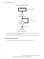
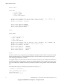
3.4 Register Write Command
A Write Command is illustrated in Figure 4. Because the interface is always using the little-endian byte format, the
byte sequences below will appear to be formatted opposite to the 32-bit word. This translation happens completely in
the background and is invisible to the user; however, the byte sequences are presented in the correct order as they
appear in sequence across the PMP interface.
MIPS® SEAD™-3 IO Processor User’s Manual, Revision 01.01
Copyright © 2009 MIPS Technologies Inc. All rights reserved.
9
3 IO Processor Software Interface
Figure 4 Register Write Command
Host Write
[Reg Write Command]
HOST_CMD = REG_WRITE
Host Write
[Register Data]
[PIC_IOCMD_RDY = 0]
Read
IO Processor
Status
Register
[PIC_IOCMD_RDY = 1]
Host Read
IO Processor Status
After the first four bytes containing the CMD ID and the translated PIC32 peripheral address are transmitted, the register payload value is transmitted via the PMP interface.
Upon assertion of the IO_RDY signal, the host reads a status word that will either be STS_OK or STS_ERR.
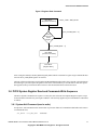
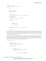
3.5 Register Read Command
The Register Read command, shown in Figure 5, is a logical inversion of the Write Command.
10
MIPS® SEAD™-3 IO Processor User’s Manual, Revision 01.01
Copyright © 2009 MIPS Technologies Inc. All rights reserved.
3 IO Processor Software Interface
Figure 5 Register Read Command
Host Write
[Reg Read Command]
HOST_CMD = REG_READ
[PIC_IOCMD_RDY = 0]
Read
IO Processor
Status
Register
[PIC_IOCMD_RDY = 1]
Host Read
[IO Processor Status]
Host Write
[Register Data]
After writing the CMD byte as REG_READ logically ORed with the virtual PIC32 register target command the host
waits for the IO_CMD_RDY signal to be asserted.
The host will then read the status word from the IO PROCESSOR and then either elect to discard or keep the data on
the following 4 byte read sequence. Regardless of the value of the STATUS byte from the PIC32 client, the register
data payload is always read from the PIC32 client to clear the transmit buffers on the IO Processor
3.6 PIC32 System Register Read and Commands Write Sequence
The PIC32 System Command write sequence is exactly the same as the PIC32 Peripheral Register sequence except
for the substation of the PIC32 System register addresses. The currently supported system commands are enumerated
as follows:
3.6.1 System Null Command (read or write)
Accepted as a valid command with no action taken. IO processor flushes all command and data buffer and returns to
a command idle state,
SYS_WRITE + SYS_CMD_NULL
0x000000
MIPS® SEAD™-3 IO Processor User’s Manual, Revision 01.01
Copyright © 2009 MIPS Technologies Inc. All rights reserved.
11
3 IO Processor Software Interface
3.6.2 System Reset Command
SYS_WRITE + SYS_CMD_RESET
0x000001
3.6.3 Firmware Version
Returns the current firmware version, which matches the version output through the serial port during startup.
SYS_READ + SYS_VERSION
0x000002
The version information returns in the data word read following the status word is
Bits [31 .. 16]
Bits [15 .. 08]
Bits [07 .. 00]
0
Major Version
Minor Version
3.7 Interrupt Support
The largest amount of virtualization in the implementation of the PIC32 IO processor implementation surrounds the
support of the interrupt system. While all peripheral specific interrupt support remains the same as defined by the
PIC32 registers, the actual PIC32 system interrupt configuration is inaccessible via the IO Processor firmware.
Upon completion of the power up cycle, the PIC32 IO Processor kernel inserts small IRQ routines at all of the available peripheral handler locations. The specific interrupt enable bits remain cleared until set by the SEAD-3 host.
When specific peripheral interrupts are enabled via the standard IO Processor interface, the PIC32 client will automatically enable or assert any remaining interrupt flags or bits required to enable the specific interrupt service
requested by the SEAD-3 core host.
Each specific interrupt service routine will assert at least one of the three hardware IRQ ID signals PIC32_IRQ_ID0,
PIC32_IRQ_ID1, PIC32_IRQ_ID2 and pass this interrupt id onto the SEAD-3 MIPS core for ISR execution.
The IRQ IDs are enumerated as follows:
0
Interrupt Source
IRQ-ID2
IRQ_ID1
IRQ_ID0
IRQ_ID
GPIO Bank A
0
0
1
0x01
GPIO Bank B
0
1
0
0x02
ADC
0
1
1
0x03
SPI1
1
0
0
0x04
SPI2
1
0
1
0x05
I2C
1
1
0
0x06
After a specific IRQ (or IRQs) have been asserted, the SEAD host can then clear each specific interrupt ID with the
PIC32_IRQ_CLR command. The format of the PIC32_IRQ_CLR is as follows:
BYTE
BYTE
BYTE
BYTE
12
3
2
1
0
PIC32_IRQ_CLR command
0
0
MASTER_CLR | IRQ_ID
MIPS® SEAD™-3 IO Processor User’s Manual, Revision 01.01
Copyright © 2009 MIPS Technologies Inc. All rights reserved.
4 PIC32 Firmware Code
If MASTER_CLR = 0x80, all pending interrupt flags are cleared. If MASTER_CLR = 0x00, the interrupt IRQ IDs
are cleared according to the individual or ORed value specified by IRQ_ID.
The application code running on the SEAD-3 host side is responsible for clearing of all peripheral specific flags and
subsequent reading of data registers, as if the application ISR were running locally.
4 PIC32 Firmware Code
The following section contains either partial or full listings of the IO Processor Firmware, with additional commentary explaining the code structure.
The following listings may not be the exact version contained in the PIC32 device on your specific SEAD-3 board. A
differences and updates will be covered in the README.TXT file packages with the source code.
The IO Processor PIC32 firmware was developed using the Microchip MPLAB IDE development environment 8.20
and Version 1.04 of the MPLAB PIC32 C Compiler. Hardware and software debugging were done using the Microchip REAL ICE hardware emulator with a custom interface cable. The wiring diagram for the custom interface cable
is shown in Section 5, "SEAD-3 IO Processor ICD Interface Cable".
The IO processor firmware consisted of two primary c source files, pic32_io_main.c and pic32_sys.c. Also required
is pic32_io.h with the rest of the standard headers being supplied by the PIC32 C Compiler development environment.
The header file pic32_io.h is self documenting in that it supplies both the constant, complex data type definitions as
described previously in this manual along with function prototypes therefore the code listing and code commentary
starts with the file pic32_io_main.c.
It is intended that the following firmware source code listings will provide a basic tutorial in PIC32 programming in
C.
As indicated in the source code license, all of the source code provided by the SEAD-3 SDK is under an open source
license and freely modifiable. It is recommended that consideration be taken if the core interface protocol is modified,
as that will have impact on all of the demo software and reference Linux ports that are available for the SEAD-3.
pic32_io_main.c
/*
SEAD3 PIC32 IO Virtual IO processor
file : pic32_io_main.c
date : 2009.01.27
MIPS Technologies
revision
0.7
0.8
*/
date
2009.01.27
2009.04.15
comment
first beta release, no interrupt support
second beta release, interruot support added
#include "pic32_io.h"
MIPS® SEAD™-3 IO Processor User’s Manual, Revision 01.01
Copyright © 2009 MIPS Technologies Inc. All rights reserved.
13
4 PIC32 Firmware Code
#define SEAD3
#ifdef EX16
// 8 Mhz crystal
// fcore = 72 MHz
// fpb = 36 MHz
// select ICD channel2
#pragma config FPLLMUL = MUL_18, FPLLIDIV = DIV_2, FPLLODIV = DIV_1, FWDTEN = OFF
#pragma config POSCMOD = HS, FNOSC = PRIPLL, FPBDIV = DIV_2
#pragma config ICESEL = ICS_PGx2
#define PIC32_CORE_CLK 72000000
#define PIC32_CORE_TIC 36000000.0
#define PIC32_PBUS_CLK 36E+06
#endif
#ifdef SEAD3
//
//
//
//
external 20 Mhz clock
fcore = 80 MHz
fpb = 40 MHz
select ICD channel1
#pragma config FPLLMUL = MUL_20, FPLLIDIV = DIV_5, FPLLODIV = DIV_1, FWDTEN = OFF
#pragma config POSCMOD = EC, FNOSC = PRIPLL, FPBDIV = DIV_2
#pragma config ICESEL = ICS_PGx1
#define PIC32_CORE_CLK
#define PIC32_CORE_TIC
#define PIC32_PBUS_CLK
80000000
40000000.0
40E+06
#endif
The above section of code is comprised mostly of configuration settings for the PIC32 device. During early development the Microchip Explorer 16 board populated with a PIC32 processor module was used, therefore the specific
clock and debug port definitions are retained.
The #pragma configs are custom extensions to the PIC32 compiler which allow specific configuration information to
be placed within the PIC32 boot ROM. As indicated in the following defines the core frequency of the PIC32 device
is set to 80.0 MHz using a 20 MHz external clock provided by the SEAD-3 clock generation circuit and the internal
PLL.
The peripheral bus frequency is obtained by dividing the core frequency by 2.
/* globals to this module */
PIC32_IO_FRAMEcmd_frame,*pframe;
unsigned pmp_data;
volatile unsigned irq_sts;
14
MIPS® SEAD™-3 IO Processor User’s Manual, Revision 01.01
Copyright © 2009 MIPS Technologies Inc. All rights reserved.
4 PIC32 Firmware Code
unsigned int *pdata;
unsigned char _debug,tx_str[80];
int main(void)
{
pframe = &cmd_frame;
pdata = &pmp_data;
_debug = 0;
init_pic32_core();
uart_puts("SEAD3 IO Processor 1.0 2009.06.12\r\n");
init_pmp_intf();
init_irq_intf();
uart_puts("IO Processor ready\r\n");
/* begin exec loop */
while(1)
{
pmp_com();
process_frame();
process_irq();
}
/* execution thread should never reach here */
while(1);
} // end main
The preceding section of code contains both the module global definitions and the main function. The executive control loop is also indicated as three successive calls to the primary state machines responsible for the SEAD-3 IO Processor communications (pmp_com), processing of the command sequences received (process_frame), and processing
the interrupt subsystem (process_irq]).
Some initial boot messages are transmitted out of the serial port however unless the global variable _debug is defined
as non zero no more messages are transmitted via the serial port. It was observed during development of this firmware that serial output during key times in execution of the pmp_com state machine will cause errors in the communication protocol between the IO Processor and the SEAD-3 bus logic.
void pmp_com(void)
{
int byte_count;
unsigned int reg_data,cmd_id;
static int pmp_state = PMP_IO_IDLE;
switch(pmp_state)
{
case PMP_IO_IDLE :
byte_count = pmp_read_data(pdata);
if(byte_count == 4)
{
cmd_id = *pdata & 0xFF000000;
MIPS® SEAD™-3 IO Processor User’s Manual, Revision 01.01
Copyright © 2009 MIPS Technologies Inc. All rights reserved.
15
4 PIC32 Firmware Code
if(cmd_id == PIC32_REG_READ)
{
if(_debug)
uart_puts("pmp state -> pic32 reg read\r\n");
pmp_state = PMP_IO_HOSTRD;
pframe -> id = *pdata & 0xFF000000;
pframe -> vaddr = *pdata & 0x00FFFFFF;
pframe -> status = FRAME_NEW;
}
The section of code above contains the first major section of the pmp_com state machine which is responsible for all
communications between the IO Processor and the SEAD-3 host core. The PMP_IO_IDLE state makes repeated calls
to the pmp_read_data function until a non zero value is returned indicating that there is possibly data sitting at the
pointer passed to pmp_read_data. Only if exactly 4 bytes (32 bits) of data was correctly passed the PMP interface
does the idle sate begin decoding the command sequence. The upper 8 bits of the data word are checked against the
valid command list, and if finding a valid command both the pmp_state is updated along with the command frame
status (pframe -> status = FRAME_NEW indicating that a new IO processor command frame is about to assembled
into the PIC32_IO_FRAME structure pointed to by pframe.
case PMP_IO_HOSTRD :
if(pframe -> status == FRAME_OK)
//frame is processed
{
if(_debug)
uart_puts("OK, -> PMP_RD_ACK\r\n");
*pdata = PIC32_STS_OK;
pmp_write(pdata);
PORTCSET = 0x0002;
pmp_state = PMP_RD_ACK;
}
else if(pframe -> status == FRAME_ERR)
{
*pdata = PIC32_STS_ERR;
pmp_write(pdata);
PORTCSET = 0x0002;
pmp_state = PMP_RD_ACK;
// bad frame
}
break;
Following the state change in pmp_com to PMP_IO_HOST_RD, we find that this state repeatedly checks the pframe
status flag indicating that the process_frame state machine has finished with the current command frame. The command frame and the pointer to it have been declared as volatile in order to remove any unwanted effects of compiler
optimizations or data cache effects. If the current frame status is returned as being of status FRAME_OK. ? While
this triggers another state change to PMP_READ_ACK, the PIC_IOCMD_RDY signal is asserted via the PORTCSET line. Also, the resulting OK status value is written into the PMP interface just before the PIC_IOCMD_RDY
flag is set.
case PMP_RD_ACK :
if(PMSTAT & PMP_OBE)
{
PORTCCLR = 0x0002;
*pdata = pframe -> regdata;
16
// check for dword read
// drop IO_RDY
MIPS® SEAD™-3 IO Processor User’s Manual, Revision 01.01
Copyright © 2009 MIPS Technologies Inc. All rights reserved.
4 PIC32 Firmware Code
pmp_write(pdata);
pframe -> status = FRAME_EMPTY;
// clear frame status
//uart_puts("host read complete\r\n");
pmp_state =PMP_IO_IDLE;
}
break;
The PMP_RD_ACK state in pmp_com continually looks at the status of the PMP port to confirm that all 32 bits have
been read by the SEAD-3 host processor. PMSTAT is a predefined status register for the PMP interface, and
PMP_OBE is the correct bit mask definition which indicates that all four transmit buffers of the PMP interface are
now empty due to a host read.
Upon detecting this condition, the PIC_IOCMD_RDY status signal is dropped back to a low state via the PORTCCLR line, while the rest of the code fragments reset the current PIC3_IO_FRAME status and reset the pmp_com state
machine back to the PMP_IO_IDLE state since this command has been completed.
// process host frames
void process_frame(void)
{
pic32_reg volatile *reg;
if(pframe -> status == FRAME_NEW)
{
pframe -> vaddr |= 0xBF000000;
switch(pframe -> id)
{
case PIC32_REG_READ :
if(( pframe -> vaddr >= 0xBF805200 && pframe -> vaddr <= 0xBF8053FF) || // I2C2
(pframe -> vaddr >= 0xBF805800 && pframe -> vaddr <= 0xBF8059FF) || // SPI1
(pframe -> vaddr >= 0xBF805A00 && pframe -> vaddr <= 0xBF805BFF) || // SPI2
(pframe -> vaddr >= 0xBF809000 && pframe -> vaddr <= 0xBF8091FF) || // ADC
(pframe -> vaddr >= 0xBF881000 && pframe -> vaddr <= 0xBF881FFF) || // ints
(pframe -> vaddr >= 0xBF886000 && pframe -> vaddr <= 0xBF8861FF)) // GPIO
{
reg = (pic32_reg*)(pframe -> vaddr);
pframe -> regdata = *reg;
pframe -> status = FRAME_OK;
if(_debug)
{
sprintf(tx_str,"valid reg read @ %08X\r\n",pframe -> vaddr);
uart_puts(tx_str);
}
}
else pframe -> status = FRAME_ERR;
break;
The above code fragment contains the first few lines of the process_frame state machine specifically looking at the
specific frame illustrated in the previous code listing sections.
MIPS® SEAD™-3 IO Processor User’s Manual, Revision 01.01
Copyright © 2009 MIPS Technologies Inc. All rights reserved.
17
4 PIC32 Firmware Code
In seeing that the current frame status has been changed to FRAME_NEW, it begins parsing the raw data contained in
the frame by first determining the command ID and then creating the actual PIC32 register address from the virtual
address and 0xBF000000.
It then checks the boundary conditions of the resulting PIC32 register to see if it’s within the allowed access ranges.
Note that as the amount of actual PIC32 peripheral address space is expanded to allow for additional functionality, it
becomes easier and quicker to use negative masking against prohibited address ranges as opposed to positive masking
against allowed ranges.
After determining that the target register is in the valid range, the actual register read operation is preformed by the
code reg = (pic32_reg*)(pframe -> vaddr).
18
MIPS® SEAD™-3 IO Processor User’s Manual, Revision 01.01
Copyright © 2009 MIPS Technologies Inc. All rights reserved.
5 SEAD-3 IO Processor ICD Interface Cable
5 SEAD-3 IO Processor ICD Interface Cable
Standard RJ11 - 6 POS Connector
Exposed contacts facing up
Wire colors of the CAT4 cable should be the
same as shown. However, the pin numbers and
signal names will always be correct.
2
3
4
5
6
NC
PGD
1
VDD
Blue - MCLR#
Green - GND
Yellow - VDD
6
MCLR#
GND
Red - PGD
Black - PGC
6
PGC
White - NC
6
2x3 .1” Molex KK series Female Header
Molex Part# 50-57-9006
Digikey Part# WM-2520-ND
Top View looking down as if plugged into SEAD-3 board
RJ11Pin
CableColor
1
2
3
4
5
6
White
Black
Red
Green
Yellow
Blue
Molex Pin Signal
6
5
4
3
2
1
n/c
PGC
PGD
GND
VDD
#MCLR
MIPS® SEAD™-3 IO Processor User’s Manual, Revision 01.01
Copyright © 2009 MIPS Technologies Inc. All rights reserved.
19
6 References
6 References
1.
MIPS32® M4K® Processor Core Software User’s Manual
MIPS document: MD00249
2.
EJTAG Specification
MIPS document: MD00047
3.
SEAD-3™ Board Schematics
MIPS document: MD00249
7 Revision History
20
Revision
Date
Description
0.05
June 16, 2009
Initial version.
1.00
July 19, 2009
Incorporate reviews.
1.01
September 8, 2011
Fix error in value of address lines
of PMP interface.
MIPS® SEAD™-3 IO Processor User’s Manual, Revision 01.01
Copyright © 2009 MIPS Technologies Inc. All rights reserved.
Copyright © 2009 MIPS Technologies, Inc. All rights reserved.
Unpublished rights (if any) reserved under the copyright laws of the United States of America and other countries.
This document contains information that is proprietary to MIPS Technologies, Inc. ("MIPS Technologies"). Any copying, reproducing, modifying or use of this
information (in whole or in part) that is not expressly permitted in writing by MIPS Technologies or an authorized third party is strictly prohibited. At a
minimum, this information is protected under unfair competition and copyright laws. Violations thereof may result in criminal penalties and fines.
Any document provided in source format (i.e., in a modifiable form such as in FrameMaker or Microsoft Word format) is subject to use and distribution
restrictions that are independent of and supplemental to any and all confidentiality restrictions. UNDER NO CIRCUMSTANCES MAY A DOCUMENT
PROVIDED IN SOURCE FORMAT BE DISTRIBUTED TO A THIRD PARTY IN SOURCE FORMAT WITHOUT THE EXPRESS WRITTEN
PERMISSION OF MIPS TECHNOLOGIES, INC.
MIPS Technologies reserves the right to change the information contained in this document to improve function, design or otherwise. MIPS Technologies does
not assume any liability arising out of the application or use of this information, or of any error or omission in such information. Any warranties, whether
express, statutory, implied or otherwise, including but not limited to the implied warranties of merchantability or fitness for a particular purpose, are excluded.
Except as expressly provided in any written license agreement from MIPS Technologies or an authorized third party, the furnishing of this document does not
give recipient any license to any intellectual property rights, including any patent rights, that cover the information in this document.
The information contained in this document shall not be exported, reexported, transferred, or released, directly or indirectly, in violation of the law of any
country or international law, regulation, treaty, Executive Order, statute, amendments or supplements thereto. Should a conflict arise regarding the export,
reexport, transfer, or release of the information contained in this document, the laws of the United States of America shall be the governing law.
The information contained in this document constitutes one or more of the following: commercial computer software, commercial computer software
documentation or other commercial items. If the user of this information, or any related documentation of any kind, including related technical data or manuals,
is an agency, department, or other entity of the United States government ("Government"), the use, duplication, reproduction, release, modification, disclosure,
or transfer of this information, or any related documentation of any kind, is restricted in accordance with Federal Acquisition Regulation 12.212 for civilian
agencies and Defense Federal Acquisition Regulation Supplement 227.7202 for military agencies. The use of this information by the Government is further
restricted in accordance with the terms of the license agreement(s) and/or applicable contract terms and conditions covering this information from MIPS
Technologies or an authorized third party.
MIPS, MIPS I, MIPS II, MIPS III, MIPS IV, MIPS V, MIPS-3D, MIPS16, MIPS16e, MIPS32, MIPS64, MIPS-Based, MIPSsim, MIPSpro, MIPS Technologies
logo, MIPS-VERIFIED, MIPS-VERIFIED logo, 4K, 4Kc, 4Km, 4Kp, 4KE, 4KEc, 4KEm, 4KEp, 4KS, 4KSc, 4KSd, M4K, M14K, 5K, 5Kc, 5Kf, 24K, 24Kc,
24Kf, 24KE, 24KEc, 24KEf, 34K, 34Kc, 34Kf, 74K, 74Kf, 74Kc, 1004K, 1004Kc, 1004Kf, R3000, R4000, R5000, ASMACRO, Atlas, "At the core of the
user experience.", BusBridge, Bus Navigator, CLAM, CorExtend, CoreFPGA, CoreLV, EC, FPGA View, FS2, FS2 FIRST SILICON SOLUTIONS logo, FS2
NAVIGATOR, HyperDebug, HyperJTAG, JALGO, Logic Navigator, Malta, MDMX, MED, MGB, microMIPS, OCI, PDtrace, the Pipeline, Pro Series, SEAD,
SEAD-2, SmartMIPS, SOC-it, System Navigator, and YAMON are trademarks or registered trademarks of MIPS Technologies, Inc. in the United States and
other countries.
All other trademarks referred to herein are the property of their respective owners.
Template: nW1.03, Built with tags: 2B
MIPS® SEAD™-3 IO Processor User’s Manual, Revision: 01.01
Copyright © 2009 MIPS Technologies Inc. All rights reserved.