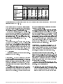
1
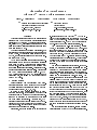
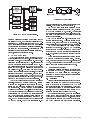
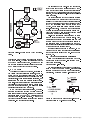
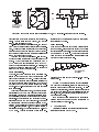
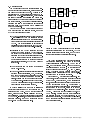
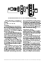
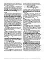
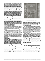
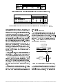
Downloaded from orbit.dtu.dk on: Dec 17, 2015
The design of an asynchronous Tiny RISC TM/TR4101 microprocessor core
Christensen, Kåre Tais; Jensen, P.; Korger, P.; Sparsø, Jens
Published in:
Advanced Research in Asynchronous Circuits and Systems, 1998. Proceedings. 1998 Fourth International
Symposium on
DOI:
10.1109/ASYNC.1998.666498
Publication date:
1998
Document Version
Publisher final version (usually the publisher pdf)
Link to publication
Citation (APA):
Christensen, K. T., Jensen, P., Korger, P., & Sparsø, J. (1998). The design of an asynchronous Tiny RISC
TM/TR4101 microprocessor core. In Advanced Research in Asynchronous Circuits and Systems, 1998.
Proceedings. 1998 Fourth International Symposium on. (pp. 108-119). IEEE. 10.1109/ASYNC.1998.666498
General rights
Copyright and moral rights for the publications made accessible in the public portal are retained by the authors and/or other copyright owners
and it is a condition of accessing publications that users recognise and abide by the legal requirements associated with these rights.
• Users may download and print one copy of any publication from the public portal for the purpose of private study or research.
• You may not further distribute the material or use it for any profit-making activity or commercial gain
• You may freely distribute the URL identifying the publication in the public portal ?
If you believe that this document breaches copyright please contact us providing details, and we will remove access to the work immediately
and investigate your claim.
The Design of an Asynchronous
TinyRISCTM TR4101 Microprocessor Core
Kare T. Christensen
1)
1)
Peter Jensen
Department of Information Technology
Technical University of Denmark
DK-2800 Lyngby, Denmark
e-mail: fktc, [email protected]
Abstract
This paper presents the design of an asynchronous
version of the TR4101 embedded microprocessor core
developed by LSI Logic Inc. The asynchronous processor, called ARISC, was designed using the same CAD
tools and the same standard cell library that was used
to implement the TR4101.
The paper reports on the design methodology, the
architecture, the implementation, and the performance
of the ARISC. This includes a comparison with the
TR4101, and a detailed breakdown of the power consumption in the ARISC.
ARISC is our rst attempt at an asynchronous implementation and a number of simplifying decisions
were made up front. Throughout the entire design
we use four-phase handshaking in combination with
a normally opaque latch controller. All logic is implemented using static logic standard cells. Despite this
the ARISC performs surprisingly well: In 0.35 m
CMOS performance is 74-123 MIPS depending on the
instruction mix, and at 74 MIPS the power eciency
is 635 MIPS/Watt.
1 Introduction
Recent research has demonstrated that asynchronous techniques have matured and can be used
to design circuits of industrial complexity with low
power consumption [17, 18, 4, 14, 13].
In order to gain broader acceptance of asynchronous techniques, it is necessary to extend the
knowledge base on where and how asynchronous design can be exploited to advantage and this calls
for more design experiments. Furthermore, CAD
tools supporting asynchronous design has to be developed and embedded in standard commercial CAD
tool frameworks. In this paper we report on a design
experiment that address both issues.
Specically, the paper reports on an asynchronous
Peter Korger
2)
2)
2)
Jens Spars
1)
LSI Logic Denmark
Lautrupvang 2B
DK-2750 Ballerup, Denmark
e-mail: fpeterj, [email protected]
re-implementation of the TinyRISCtm TR4101 embedded microprocessor core [6] developed and marketed by LSI Logic Inc. as part of their CoreWare
macro cell library [5]. The TR4101 implements the
MIPS-II and the MIPS16 instruction sets [9, 8].
The asynchronous re-implementation, called
ARISC, was designed from scratch in a 1 man-year
eort over a period of 5 months, in a joint project between the Technical University of Denmark and LSI
Logic Denmark [1]. The work was carried out within
LSI Logic using the CAD-tools and standard cell libraries available in that organization. The end result
of this work is a placed and routed standard cell layout from which speed and power gures have been
extracted.
The paper makes several contributions. It demonstrates how asynchronous design is feasible in a traditional CAD tool environment based on the Verilog
hardware description language and the Synopsys synthesis tool. These tools were used to describe the
design and to synthesize the data-path logic. The
(speed-independent) asynchronous control logic was
designed partly by hand and partly by using the tool
Petrify [2]. Furthermore, the paper develops a simple
and ecient architecture whose implementation performs better than the TR4101. Given that the latter
is a highly optimized design and that the ARISC is
a quick rst attempt at an asynchronous implementation (with signicant room for improvement), this
is a promising result. The paper reports speed and
power measures for the ARISC and compares these
with the TR4101. Finally, the paper gives a detailed
breakdown of the power consumption of the ARISC,
thereby providing some hints for further improvement
and some guidelines for asynchronous design in general.
The paper is organized as follows. Section 2 gives a
brief description of the TR4101 microprocessor core.
Authorized licensed use limited to: Danmarks Tekniske Informationscenter. Downloaded on June 01,2010 at 11:07:41 UTC from IEEE Xplore. Restrictions apply.
Figure 2: TR4101 pipeline
Figure 1: TR4101 in a typical system.
Section 3 describes the design methodology used in
the design of ARISC, and following this section 4 describes the RTL level architecture of the ARISC. Section 5 provides some information about the physical
implementation and section 6 presents the results i.e.
the speed and power measures. This is followed by a
discussion of the experiences and results in section 7.
Finally, section 8 concludes the paper.
2 The TR4101 core
The TR4101 [6] is a small and exible 32-bit MIPS
microprocessor aimed at the low-end of the embedded
processor market. It implements the 32-bit MIPS-II
instruction set architecture (ISA) [9], as well as the
MIPS16 application specic extension (ASE) 16-bit
compressed instruction set [8]. The MIPS16 ASE is a
subset of the MIPS-II ISA where each instruction is
compressed to 16-bit. This has a number of advantages: The code density almost doubles, and this has
signicant inuence on memory size, memory bandwidth and power consumption. The MIPS16 ASE is
the target instruction set for the TR4101, but MIPS-II
code and MIPS16 code can be mixed arbitrarily.
The TR4101 does not include memory management
facilities, caches or a multiply/divide unit. Instead
a library of macro-cells [5] are available to the designer who can tailor the processor for the particular requirements. Figure 1 shows a typical system
where a number of such macro-cells have been added.
The FlexLink interface in the left side of gure 1 enables users to add modules to the execute stage of
the TR4101 instruction pipeline, thereby allowing for
customer specic instructions like multiply and divide. Such modules are called Computational Bolt
On (CBO) modules. The TR4101 has a single 32-bit
memory interface for both instruction fetches and data
accesses - the CBus in the middle of gure 1.
The TR4101 has a three stage pipeline with the
following stages: Instruction Fetch (IF), Execute
(X1/X2) and Writeback (WB), gure 2. This implies
that all instructions execute in one cycle, except Load
and Store which execute in two cycles (X2 is a stall
cycle for data accesses).
The TR4101 fetches one 32-bit instruction word
for each instruction fetch. This also applies for the
MIPS16 mode, even though only 16 bit are used, i.e.
decompressed into a 32-bit instruction and executed.
The TR4101 is fabricated in LSI Logic's G10ptm
technology which is a 3.3V, 0.35 m CMOS process.
It is able to run at a clock rate of 81 MHz and for a
typical code mix with 30% load/store this corresponds
to 62 MIPS, assuming a cache hit for every memory
access.
At the circuit level extensive clock gating is used
in order to minimize power consumption. Furthermore, LSI Logic has added a new MIPS-II instruction,
WAITI, (wait for interrupt) that puts the TR4101 into
sleep mode where it consumes almost no power.
3 Design methodology
This section presents the design methodology used
in the design of the ARISC. This includes the use of
the standard CAD tools Verilog and Synopsys, and
technology mapping of asynchronous control circuits
onto a standard cell library.
3.1 Baseline
As the available resources were limited and as the
design was carried out within LSI Logic it was decided to take maximum advantage of the CAD tool
framework available in that organization. Apart from
the circuit level design of the asynchronous control
circuits, the ARISC is designed using the same CAD
tools that has been used to design the TR4101.
On the asynchronous side, a number of decisions
were made up front in order to simplify the design:
Throughout the entire design a four-phase bundled
data protocol is used and with only a few exceptions
the ARISC uses normally opaque latch controllers.
Authorized licensed use limited to: Danmarks Tekniske Informationscenter. Downloaded on June 01,2010 at 11:07:41 UTC from IEEE Xplore. Restrictions apply.
Figure 3: Design-ow used for the ARISC implementation.
Furthermore, all modules in the design are equipped
with input latches. This is a simple strategy aiming
at minimum power consumption. In order to meet
the bundling constraint (request before data) we used
a 50 % safety margin for the matched delays.
3.2 CAD tools
The design ow is shown in gure 3. It is based on
the Verilog hardware description language, in combination with the Synopsys synthesis tools. The initial
high level model is separated into data path and control structures. These are synthesized separately, and
subsequently combined into a single netlist of standard cells. Delay estimations from this netlist is used
for insertion of proper matched delays. Finally placement and routing is performed, and power and speed
measures are extracted from the layout.
In the high level Verilog specication, the asynchronous handshaking between modules was modelled using abstract channels, described in Verilog as
procedures called SEND and GET (corresponding to
an event based two-phase protocol). This way the
high level model is completely decoupled from specic
handshake- and implementation details.
The separation of the data-path and control circuitry within each of the modules was done by hand.
From the high level Verilog code it was a fairly simple
task to derive RTL-level Verilog code for the data-path
circuitry, and to synthesize gate-level implementations
using Synopsys.
The control circuitry in the modules was typically
also partitioned into a logic block that could be synthesized by Synopsys and an asynchronous control circuit that was specied as a Signal Transition Graph
(STG) and synthesized using the tool Petrify [2] or
by hand. In the latter case Petrify was used to verify
speed-independence. To support the implementation
of these asynchronous control circuits a large number of (asymmetric) C-elements were built from gates
available in the standard cell library.
Post-layout simulations were performed to check
the 50% safety margin of the matched delays. Also,
all signals were checked for excessive rise and fall
times in order to avoid timing problems related to
the isochronic forks. It also ensures that the handshake protocols (data before request) are not violated
by the actual implementation/layout.
Functional testing was done by running 1.18 MB
binary code of ocial MIPS test programs exercising
the back annotated netlist with MIPS-II and MIPS16
code [10, 11].
3.3 Asynchronous circuit primitives
Using LSI Logic's standard cell library we implemented a set of (asymmetric) C-elements and a number of latch controllers.
Asymmetric C-elements.
The logic expressions for the Qset and Qreset functions of more than 30 asymmetric C-elements were
specied manually and mapped onto the cell library.
Surprisingly, most asymmetric C-elements with two
Figure 4: Example of an asymmetric C-element implemented using an OAI-gate and an inverter.
Authorized licensed use limited to: Danmarks Tekniske Informationscenter. Downloaded on June 01,2010 at 11:07:41 UTC from IEEE Xplore. Restrictions apply.
Figure 5: The normally opaque latch controller: Symbol, STG and speed-independent implementation.
inputs and some with three inputs had good gate mappings. An example is shown in gure 4, and the full
set of C-elements is found in [1].
C-elements are state holding elements, and some of
them have to be set or reset during system initialization. The set and reset functionality can be incorporated into the gate implementation by simply including the set and reset inputs in the logic expressions as
shown in the example in gure 4.
Another method can be used if the C-element without set and reset functionality has an inverter in the
output. Then the inverter can be replaced with a
NAND gate to add set functionality and with a NOR
gate to implement reset functionality. In general, the
addition of a set or a reset input tend to reduce the
speed and the output drive capability.
troller is that it works equally well with latches and
edge triggered ip ops.
Delay elements.
More than 20 predened asymmetric delays ranging
from 300 ps to 6.0 ns were implemented by composing
conventional standard cells. The delay elements were
made as shown in gure 6. The small propagation
delay for high to low transitions makes the reset phase
of the four phase handshaking fast.
Latch controllers.
The long-hold fully decoupled latch controller presented in [3] was mapped onto the cell library and
used in a few places in the ARISC. The semi decoupled
and the fully decoupled latch controllers presented in
the same paper were also implemented, but they were
not used due to the poor performance of the threeand four-input C-elements needed to implement these
latch controllers.
To reduce power consumption, the majority of latch
controllers in the ARISC are normally opaque latch
controllers. Figure 5 shows the signal transition graph
and a speed independent implementation of this latch
controller. It was developed and optimized to use Celements with only two and three inputs. The actual
implementation has been optimized further: By exploiting a timing relation between the input signals
to the C-element labelled C2, and by reshuing some
\inversion bubbles," C2 has been replaced by a 3-input
NAND gate. Another advantage of this latch con-
Figure 6: Delay element with fast high-to-low propagation delay.
By using AND gates with strong output transistors
and weak input transistors, fairly high delays with acceptable power consumption were achieved. It also
gives good predictability, because internal gate delays
dominate (when strong output transistors drive small
loads). In fact, the post layout delays were within 10%
of the expected values.
Some additional delay elements with controllable
delays were made in order to allow exploitation of
varying delays in the data-path.
4 Architecture
This section presents the internal architecture and
instruction execution of the ARISC.
Authorized licensed use limited to: Danmarks Tekniske Informationscenter. Downloaded on June 01,2010 at 11:07:41 UTC from IEEE Xplore. Restrictions apply.
TR4101 co-processors connect to the synchronous
C-bus (see gure 1) and the associated control
signals are closely linked with the internal structure of the synchronous three stage pipeline of the
TR4101. For obvious reasons an asynchronous
processor can not implement this, and the ARISC
does not provide any support for co-processors.
Extensions to the TR4101 execution unit like
multiply and divide units (in TR4101 terminology called Computational Bolt On modules) are
connected to the FlexLink interface (see gure 1).
This is a simple synchronous interface and it
would be straightforward to implement a similar
asynchronous interface, but the ARISC does not
include this.
ARISC supports only big endian byte ordering
within a 32-bit word.
The MIPS-II instruction set architecture includes
a system control coprocessor, CP0, implementing memory management and exception handling.
The TR4101 includes the exception handling facilities, whereas memory management is handled
by an optional co-processor (gure 1 bottom left).
ARISC implements none of this, but its architecture does take exceptions into account.
It must be stressed that the above omissions are
merely simplications that do not inuence the architecture of the ARISC. Nor do they inuence the
speed, power and area gures presented in the following sections. Apart from instructions implemented
by TR4101 co-processors, and instructions related to
exception handling, the ARISC implements the full
MIPS-II and MIPS16 instruction sets.
Inst
I
Cache
ARISC
Data
D
Cache
Mem
Inst
ARISC
Data
Bus Interface
(a)
Cache
Mem
(b)
Asynchronous
Inst
ARISC
Data
Synchronous
Synchronizing
Bus Interface
Low power consumption and architectural simplicity was favoured over performance, as long as the latter was not compromized too much. This led to an
architecture with multiple execution units and a restricted form of out-of-order execution. Data hazards
are solved by stalling the processor and branch hazards are solved by ushing the instruction pipeline if
the branch is taken. The penalty of these simple solutions is minimized by the parallel and asynchronous
execution units, in combination with a register le
with two write ports.
As the ARISC project was a design experiment
with a limited time and resource budget, a number
of TR4101 features were omitted:
Bus Interface
4.1 Introduction
Cache
Mem
(c)
Figure 7: ARISC Congurations: (a) With separate
asynchronous instruction and data caches, (b) With
a single shared asynchronous cache, and (c) with a
synchronous interface to a single shared cache.
The ARISC is designed as a Harvard architecture
with separate instruction- and data memory ports.
These interfaces are asynchronous. ARISC can be
used - and has been simulated - in a number of congurations as shown in gure 7. In the following we
refer to these as conguration A, B, and C, respectively. The dashed memory boxes in gure 7(a)-(b)
indicate that simulations assume 100% cache hits, i.e.
the rest of the memory system is ignored.
Conguration A, with separate instruction- and
data caches, is used to establish the speed potential
of the ARISC. Conguration B, with a single shared
cache, is the asynchronous equivalent to the standard
TR4101 conguration (gure 1). Conguration C,
with a synchronizing bus interface and a single shared
synchronous memory module, allows us to take advantage of the Verilog test-bench developed for the
TR4101. Using data for LSI Logic's G10p 0.35m
CMOS process, we estimate that the synchronizing
bus interface in gure 7(c) would require 2.2 ns. for
reliable synchronization. This means that conguration C is actually practically feasible (although it is
not the ideal situation).
Authorized licensed use limited to: Danmarks Tekniske Informationscenter. Downloaded on June 01,2010 at 11:07:41 UTC from IEEE Xplore. Restrictions apply.
Logic
Shift
CP0
Issue
Flush
Inst.
Mem.
Decode
Lock
REG
Read
Arith.
PC
Read
PC
ALU
Data
Mem.
UnLock
REG
Write
Bolt
On
Figure 8: Internal architecture of the ARISC (black boxes represent latches/registers).
Following these remarks on the externals of the
ARISC, we now turn our attention to its internal architecture.
4.2 The ARISC data path
Token ow.
The basic pipeline structure for the conguration with
asynchronous interfacing to the caches (gure 7(a)) is
shown in gure 8. It is essentially a fetch-decode ring
with a xed number of tokens forking o instructions
for execution. Each token corresponds to a 32-bit instruction word, and with two tokens in the ring one
instruction is being prefetched.
When a synchronizing bus interface is used (gure 7(c)) the ring latency is higher and therefore three
tokens are needed to maintain throughput. In this situation two instructions are prefetched. The communication of control information between the functional
units in the fetch-decode ring is handled by a number
of tag bits associated with the tokens.
The fetch-decode ring works as follows. When an
address of a 32-bit instruction word has been calculated in the PC ALU it is held by the PC register (leftmost in gure 8). Then the instruction word is fetched
from the instruction cache and passed to the decode
unit. Here the instruction is decoded and passed on
to the ush unit.
Under normal execution the ush unit works as
a register holding the decoded instruction while
operands are being fetched from the register le and
from the PC registers (four old PC values are held in
four 30-bit wide shift registers). The issue block is responsible for issuing instructions for execution as soon
as the necessary operands are ready. This means that
a load immediate instruction can be issued almost instantaneously, while a normal R-type instruction can
not be issued until the register le read has been performed. Besides this, the issue block is also responsible for initiating a new instruction address calculation
and thereby a new instruction fetch every time a 32bit instruction word has been used (i.e. decoded and
released for execution). In this way the number of
tokens in the fetch ring is kept constant.
Basic instruction execution.
The issue block passes the instruction to the relevant
execution unit, see gure 8. The use of parallel execution units with normally opaque latch controllers in
the input, reduces the power consumption and enables
faster instruction execution.
The execution units are divided into two major
groups: The fast operations (arithmetic, logic, and
shift operations) and the slow operations (load, store
and computational bolt-on's such as multiply/divide).
Each of these two groups has its own write back port
to the register le. This approach gives very good
write back bandwidth, and automatically enables outof-order execution.
To avoid data hazards the register le includes a
locking mechanism. When the issue unit is about to
issue an instruction that writes a result into a register,
that register is locked, and when the instruction later
writes its result, the register is unlocked again. If a
subsequent instruction needs data from a register that
is locked, the instruction is simply held back by the issue block until the register is unlocked, and the correct
operand is available. This is a simple and well known
strategy, but the parallel and asynchronous execution
Authorized licensed use limited to: Danmarks Tekniske Informationscenter. Downloaded on June 01,2010 at 11:07:41 UTC from IEEE Xplore. Restrictions apply.
units in combination with the two write ports on the
register le makes the performance penalty moderate.
4.3 Branch and Jump
The ush unit is controlled by a small state machine whose operation is controlled by the tags that
are associated with the tokens circulating in the fetchdecode ring. Under normal execution it simply holds
the instructions while operands are being read in the
register le and in the PC shift register.
Branch.
When a branch instruction is encountered, the branch
condition is evaluated in the issue block. If the branch
condition is false, the normal sequential instruction
execution simply proceeds. If the branch condition is
true the issue block will issue a branch calculation request to the address calculation ALU. After this the
ush unit will start converting subsequent instructions
into NOPs (by simply clearing a small number of control signals). This way the issue block can continue
to issue address calculation requests to the PC ALU
and thereby the number of tokens in the fetch-decode
ring is kept constant. After some time, the instruction
fetched from the branch target address arrives to the
ush unit and here a tag bit, originally appended by
the PC ALU, instructs the ush unit to stop ushing
immediately.
If a branch-likely instruction is not taken, the ush
unit will ush the next instruction and then automatically resume normal execution.
Jump.
When a jump instruction is encountered the following
instruction (i.e. the instruction in the jump delay slot)
is allowed to pass the ush unit and then instructions
are ushed until the instruction at the jump target
address arrives (with a tag-bit indicating that ushing
should cease).
The branch and jump mechanisms described above
results in some unnecessary instruction decoding, but
it ensures a simple and fast unidirectional processing
ow in the fetch-decode ring.
4.4 MIPS16 instructions
When the ARISC operate in MIPS16 mode two instructions are fetched in each instruction cache read.
This gives a high instruction fetch bandwidth and an
option to raise the instruction execution rate. Furthermore power is saved by invoking the program counter
and the instruction cache only once for every other
instruction.
The ARISC fetch-decode ring handles MIPS16 instructions as follows. From the instruction cache 32-
bit words are passed on to the decoder along with a
few tag bits indicating the instruction to be decoded:
1) A 32-bit MIPS-II instruction
2) A MIPS16 instruction - 1st. halfword
3) A MIPS16 instruction - 2nd. halfword
The decoder will issue a token to the execute unit
for every instruction (where this is required), but the
issue unit issues a token to the PC ALU only when
a MIPS16 instruction from the 2nd halfword is issued
for execution.
Apart from the decode unit, all other units
work independently of the operating mode (MIPSII/MIPS16). This gives a simple data ow with high
speed and low power consumption as a result.
4.5 Exceptions and Reset.
Reset.
After a global reset, a jump to the reset exception
vector must be performed. This is done by emulating a
jump register (JR) instruction and replacing the target
address by an exception vector provided by a small
ROM in the issue unit.
Exceptions.
As mentioned earlier, exception handling is currently
not implemented in the ARISC. The following outlines how exceptions could be dealt with, and argues
that exception handling is possible with a marginal
performance penalty.
Common to all the exceptions is that they can be
implemented by emulating JR instructions using the
same circuitry that is used for the global reset.
When an exception instruction such as a trap, a
break or a sys-call occurs, the correct PC value is written to the EPC status register in the system control
coprocessor (CP0). At the same time the exception
is taken by emulating a JR instruction to the appropriate exception vector. These actions are taken by
reusing the same circuitry as used for the global reset.
External interrupts could be handled in the same way
by the decode unit.
Internal exceptions arising in one of the execution
blocks; i.e., an arithmetic overow in the arithmetic
block (c.f. gure 8) or a memory reference error in
the data memory block are a little more involved. The
problem is that after being issued sequentially in program order, instructions execute in parallel and write
backs may occur out of order in a non-deterministic
way. A simple solution to this problem is to adopt
a policy allowing only a single instruction that may
cause an interrupt, to be in execution at any time.
This requires a positive or negative feed back from
Authorized licensed use limited to: Danmarks Tekniske Informationscenter. Downloaded on June 01,2010 at 11:07:41 UTC from IEEE Xplore. Restrictions apply.
the relevant execution unit to the issue unit. The issue unit may continue to issue instructions whose execution can not result in an exception. In this way
the processor may execute one or two instructions following the instruction that caused the exception (before the exception handler is invoked). Because of the
register locking, there will be no data-hazards, and
program execution stops with the machine in a well
dened state (from which it is possible to recover).
Such a policy has a performance penalty, but it will be
marginal: signed arithmetic instructions account for
less than 0.5-1.0% of all instructions, and loads and
stores to the data memory are done sequentially anyway. As arithmetic instructions that can cause overow exceptions are so rare, it is even possible to stop
instruction-issuing completely until an OK is received
from the arithmetic block. This is cleaner and it is the
solution we envision.
Memory reference exceptions related to instruction
fetching is another issue. As the number of tokens in
the fetch-decode ring is xed, and as instructions are
fetched sequentially in program order, everything is
deterministic and there is no fundamental diculties
in dealing with these exceptions.
4.6 Power down modes
The power down modes described below were not
implemented in the nal ARISC but they are easily
added once exceptions have been implemented.
WAITI.
A \wait for interrupt" instruction has been added to
the MIPS-II instruction set by LSI Logic. This instruction stalls the CPU completely until an interrupt
or a reset occurs, thereby bringing power consumption to zero. As ARISC does not include exception
handling the WAITI-instruction is not supported, but
there would be no fundemantal problems in implementing it.
Voltage scaling.
Some unused bits in a status register in the CP0
unit could be used to hold information about the
current need for processing speed. In this way scaling/selection of the supply voltage [12] under program
control would be possible. For instance the ARISC
could be operated at 1.8 V when the need for processing speed is low, and at 3.3 V in the normal case when
higher processing speed is required. This would give
considerable power savings without compromising the
availability of high speed operation.
Large selectable delay.
Yet another possibility would be to implement a large
selectable delay e.g. 100 ns. in one of the pipeline
Figure 9: Layout of the ARISC
stages of the instruction fetch-decode ring. This way
a status bit could control the selectable delay and
thereby either turn a \slow mode" on or o.
5 Implementation
The ARISC architecture was designed, synthesized,
laid out, and functionally veried, in one man year
over a ve month period. This accomplishment was
mainly due to the presence of a test environment which
made thorough testing possible. The modularity of
asynchronous circuits also helped achieving a working
design in a short time.
Figure 9 shows the layout of the ARISC. Text
marks where the various internal blocks of the processor are placed on the oor-plan. Mapped to the
LSI Logic 0.35 m G10ptm technology the area of
the ARISC CPU core is 2.2 mm2 of which the register
le covers 0.4 mm2.
From the layout, load capacitances for gates and
wires were extracted. This information was back annotated and used for simulations with the Verilog gate
netlist. This resulted in realistic and accurate power
and speed measurements.
6 Results
The ARISC is simulated in three congurations A,
B and C (see gure 7). The best performance is
achieved with the asynchronous caches, because no
synchronization is necessary for each cache access.
6.1 Performance
Two benchmark sets were run to measure the speed
and the power consumption of the ARISC. Both
Authorized licensed use limited to: Danmarks Tekniske Informationscenter. Downloaded on June 01,2010 at 11:07:41 UTC from IEEE Xplore. Restrictions apply.
Instruction frequency
Data
Benchmark Load Store Jump+Branch Other Hazards
Peak
17 % 17 %
0%
66 %
0%
Stanford
37 % 18 %
10 %
35 %
15 %
Table 1: Instruction and data hazard frequencies in the two benchmark program sets.
Benchmark
Stanford
Peak
Conguration
MIPS mW MIPS/W MIPS
ARISC conguration A
74 117
635
123
ARISC conguration B
72
ARISC conguration C (@ 83 MHz) 41
103
TR 4101 (@ 83 MHz)
48
89
539
62
Table 2: Performance of the ARISC and the TR4101 (extracted from the layouts; VDD = 3.3 V).
below 13.5 ns.
6.2 Power breakdown
The power consumption of the TR4101 and the
ARISC was measured using the QuickPower tool from
Mentor Graphics, with the ARISC running the Stanford benchmark compiled to MIPS16 code. The measurements were done using conguration C with a bus
frequency of 10 MHz, and the results are shown in
table 3. The six sources of power consumption are
dened/explained in gure 10.
P_other_control
P_delay
P_ctl
Control
Data-Path
P_buf
En
P_logic
P_latch
benchmarks sets were compiled to MIPS16 code. The
characteristics of the two benchmarks are shown in
table 1. The Peak benchmark set measures the full
potential of the ARISC, exploiting its ability to execute several instructions concurrently. The Stanford
benchmark set includes the following classic benchmarks: \Perm", \Towers", \Queens" and \Puzzle."
As the Stanford benchmark has a high number of
load/store instructions and data hazards, it results in
somewhat pessimistic performance gures. Therefore
the speed measures resulting form the Peak and the
Stanford benchmarks correspond to an upper and a
lower bound on performance. The benchmarks are
small \toy programs" that runs with a 100 % cache
hit ratio, but this is exactly what is needed to compare the CPU-time and MIPS rating of the ARISC
and the TR4101 (because they implement the same
instruction sets).
The measured speed and power gures are shown
in table 2. It is noted, that under optimal conditions
(conguration A running the Peak benchmark) the
ARISC performs signicantly better than the TR4101.
In the synchronous TR4101 conguration (conguration C), the ARISC performance is only 41 MIPS
due to the high occurrence of load/store instruction in
the code. With a more \optimistic" code the performance of the ARISC will approach 123 MIPS, which is
the performance of the above mentioned Peak benchmark.
The inuence of the cache access time on the performance depends on the type of code that is run. When
running peak code in conguration A the ARISC will
run at 123 MIPS as long as the cache access time is
Figure 10: The six sources of power consumption.
The control structures consume as much as 30% of
the total power while 25% is consumed by latches and
registers. Only 42% of the power consumption is used
doing the actual computations. The relatively high
Authorized licensed use limited to: Danmarks Tekniske Informationscenter. Downloaded on June 01,2010 at 11:07:41 UTC from IEEE Xplore. Restrictions apply.
Power [mW]
Data Path
Asynchronous control
Module
Ptotal Plogic Platch Pbuf Pctl Pdelay Pother
Decoder
3.98 2.26 0.98 0.06 0.13 0.35 0
Execute
2.13 0.50 0.60 0.18 0.40 0.35 0.10
Program Counter 1.41 0.18 0.77 0.03 0.11 0.17 0.15
Register le
1.58 0.35 0
0
0
0.30 0.93
Flush
0.85 0.17 0.54 0.03 0.11 0
0
Issue
1.82 1.49 0
0
0
0.02 0.031
ARISC
11.77 4.95 2.89 0.30 0.75 1.19 1.69
Total
100 % 42 % 25 % 3 % 6 % 10 % 14 %
Table 3: Breakdown of power consumption in the ARISC (Stanford benchmark; Conguration C with a 10 MHz
instruction cache; VDD = 3.3 V).
power consumption in the matched delays is caused
by the long chains of and-gates in the implementation
(gure 6). Only 3% of the power is used for driving
the enable/clock lines of the storage elements.
In the above measurements, the ARISC uses normally opaque latch controllers to minimize switching
activity in idle modules. If normally-transparent latch
controllers were used the power consumption would
almost double to 22.7 mW. This conrms the importance of gating o idle sections of the CPU.
6.3 Area
Compared to the 2.2 mm2 of the ARISC, the synchronous TR4101 occupies 1.6 mm2. The dierence is
mainly due to more pipelining and decoupling latches
in the ARISC. As the design of the ARISC is a rst
attempt on an asynchronous implementation and as
our experience using Synopsys was limited, the area
dierence could no doubt be reduced signicantly.
7 Discussion
This section discuses the most important experiences from the ARISC design.
Methodology. The use of Verilog for high level
modelling of asynchronous circuits proved to be a viable and reasonably ecient approach. At the early
stages in the design, where it is important to identify
potential bottlenecks and act against them, we used
delay estimates for the dierent blocks and simulated
the design.
In a more complex design than the ARISC, it would
be desirable to have more automated and interactive
techniques and tools to analyze the dynamics of the
token ow in the design. This would provide better
support for decisions regarding insertion of latches and
balancing of pipeline stages.
Our experience from using Synopsys to synthesize
the data-path blocks are more mixed. The gate count
of the resulting circuits depends heavily on the specied timing constraints, and it is necessary to iterate the synthesis to get acceptable results. A general experience is that by loosening the timing constrains slightly, Synopsys often produces a circuit with
a much lower gate count, and a signicantly lower
power consumption. In this way the power consumption of the ARISC was reduced 20% by re-synthesizing
logic blocks not in the critical path.
Architecture. The simple architecture of the
ARISC with its parallel execution stages proved to
perform well and allowed us to avoid data forwarding,
branch prediction and other features that complicate
the design, and increase the power consumption.
Handshake protocol and latch controllers. The
systematic use of four-phase handshaking in combination with normally opaque latch controllers represents a great simplication of the design process. It
also resulted in a signicant reduction of the power
consumption, as compared with the use of normally
transparent latch controllers.
There is however a performance penalty, and eliminating some of the performance bottlenecks should be
considered. Some possibilities are:
Local use of two-phase handshaking would elimi-
nate the return to zero delay, but unless the control ow is relatively simple the advantage may
easily diminish due to the more complex event
Authorized licensed use limited to: Danmarks Tekniske Informationscenter. Downloaded on June 01,2010 at 11:07:41 UTC from IEEE Xplore. Restrictions apply.
based control logic [15]. Furthermore, the use of
two-phase handshaking would allow some of the
power hungry asymmetric delay elements to be replaced with simpler symmetric ones. A disadvantage is that a much larger set of latch-controllers
would be required, including conversion from twophase to four-phase handshaking and vice versa.
Local use of normally transparent latch controllers
that has a lower forward latency is another option. It might result in a signicant increase in
power consumption, but often the \congestion"
of tokens around a performance bottleneck will
limit this eect.
Standard cell library. The use of a traditional
standard cell library did not cause any signicant
problems. We were able to develop a set of asymmetric C-elements and Latch controllers with good performance.
If a larger selection of latch controllers is needed the
need for more complex generalized C-elements may
arise, and it may not be possible to provide ecient
implementations of these.
Finally we notice that our asymmetric matched delays are fairly insensitive to wiring delays, but that
this comes at the expense of a high power consumption. The development of a special asymmetric-delay
standard-cell should be considered.
ARISC performance. Depending of the bench-
mark set, the performance (MIPS) of the ARISC is
50-90% better than the TR4101, and excluding the
register le the area of the ARISC is 50 % larger than
the area of the TR4101. This reects the fact that the
ARISC has deeper pipelines, parallel execution units,
and more control logic.
The MIPS/Watt ratings of the ARISC is 17% better than the TR4101. As the TR4101 is a mature industrial design employing extensive clock gating, and
as the ARISC is a rst attempt at an asynchronous
implementation (representing a small one man-year
eort), it is likely that the 17 % dierence could be
improved by a signicant amount.
Finally we notice that the dierence in power consumption (mW) is less than the dierence in area; the
switching activity in circuits in the ARISC is lower
than in the TR4101. This is consistent with what
have been observed in other asynchronous designs.
A comparison with other recent asynchronous processor designs [4, 7, 16] is tempting, but dierences in
architecture, circuit implementation style, and technology, makes such a comparison meaningless.
8 Conclusion
The paper described the design of an asynchronous
version of the TR4101 embedded microprocessor core
developed by LSI Logic Inc. as part of their CoreWare
macro cell library.
The asynchronous processor, ARISC, was designed
from scratch in a one man year eort over a period
of ve months. The design used the same tools (Verilog and Synopsys) and standard cell library, that was
used to implement the TR4101. The design use fourphase handshaking and normally opaque latch controllers throughout the entire design. Altogether this
leaves plenty of room for improvement, and viewed in
this context the ARISC performs surprisingly well: In
0.35 m CMOS performance is 74-123 MIPS depending on the instruction mix, and at 74 MIPS the power
eciency is 635 MIPS/Watt. This is somewhat better
than the TR4101, and given that they implement the
same instruction set and that they were designed using
the same tools, this shows that asynchronous design
is a viable route to low power consumption.
In addition to these results, the paper presented
a simple and ecient asynchronous architecture, a
simple design methodology based on traditional CAD
tools, and a detailed set of speed and power measures.
References
[1] Kare Tais Christensen and Peter Jensen. An
Asynchronous Low Power RISC CPU. Master's
thesis, Department of Information Technology,
Technical University of Denmark, 1997. IT-E 749.
[2] Jordi Cortadella, Michael Kishinevsky, Alex
Kondratyev, Luciano Lavagno, and Alexandre
Yakovlev. Petrify: a tool for manipulating
concurrent specications and synthesis of asynchronous controllers. In XI Conference on Design
of Integrated Circuits and Systems, Barcelona,
November 1996.
[3] S. B. Furber and P. Day. Four-phase micropipeline latch control circuits. IEEE Transactions on VLSI Systems, 4(2):247{253, June 1996.
[4] S. B. Furber, J. D. Garside, S. Temple, J. Liu,
P.Day, and N. C. Paver. AMULET2e: An Asynchronous Embedded Controller. In Proc. International Symposium on Advanced Research in Asynchronous Circuits and Systems, pages 290{299.
IEEE Computer Society Press, 1997.
[5] LSI Logic Corporation. TinyRISCtm TR4101
Building Blocks - Technical Manual. Order Number C14037.
Authorized licensed use limited to: Danmarks Tekniske Informationscenter. Downloaded on June 01,2010 at 11:07:41 UTC from IEEE Xplore. Restrictions apply.
[6] LSI Logic Corporation. TinyRISCtm TR4101
Microprocessor Core - Technical Manual. Order
Number C14038.
[7] A. J. Martin, A. Lines, R. Manohar, M. Nystrom,
P. Penzes, R. Southworth, U. V. Cummings, and
T-K. Lee. The Design of an Asynchronous MIPS
R3000. In Proceedings of the 17th Conference on
Advanced Research in VLSI, pages 164{181, 1997.
[8] MIPS Technologies, Inc. Product Description,
MIPS16 Application-Specic Extension, Revision
1.3. 30.01.97.
[17] C. H. van Berkel, Ronan Burgess, Joep Kessels,
Ad Peeters, Marly Roncken, and Frits Schalij.
Asynchronous Circuits for Low Power: a DCC
Error Corrector. IEEE Design & Test, 11(2):22{
32, 1994.
[18] Kees van Berkel, Ronan Burgess, Joep Kessels,
Ad Peeters, Marly Roncken, Frits Schalij, and
Rik van de Viel. A single-rail re-implementation
of a dcc error detector using a generic standardcell library. In 2nd Working Conference on Asynchronous Design Methodologies, London, May 3031, 1995, pages 72{79, 1995.
[9] MIPS Technologies, Inc. R10000 Microprocessor
User's Manual, Version 1.1. 04.12.96.
[10] MIPS Technologies, Inc. R4000 Architecture Test
Verication (ATV) suite, 1989.
[11] MIPS Technologies, Inc. MIPS16 Architecture
Test Verication (ATV) suite, 1996.
[12] L. S. Nielsen, C. Niessen, J. Spars, and C. H. van
Berkel. Low-power operation using self-timed circuits and adaptive scaling of the supply voltage.
IEEE Transactions on VLSI Systems, 2(4):391{
397, 1994.
[13] Lars S. Nielsen and Jens Spars. An 85 W Asynchronous Filter-Bank for a Digital Hearing Aid.
In Proc. IEEE International Solid State circuits
Conference, 1998. (To Appear).
[14] Lars Skovby Nielsen. Low-power Asynchronous
VLSI Design. PhD thesis, Department of Information Technology, Technical University of Denmark, 1997. IT-TR:1997-12.
[15] Jens Spars, Christian D. Nielsen, Lars S.
Nielsen, and Jrgen Staunstrup. Design of
self-timed multipliers: A comparison. In
S. Furber and M. Edwards, editors, Proc. of
IFIP TC10/WG10.5 Working Conference on
Asynchronous Design Methodologies, Manchester, England, 31 March { 2 April 1993, pages
165{180. Elsevier Science Publishers B. V. (IFIP
Transactions, vol. A-28), July 1993.
[16] A. Takamura, M. Kuwako, M. Imai, T. Fujii,
M. Ozawa, I. Fukasaku, Y. Ueno, and T. Nanya.
TITAC-2: An asynchronous 32-bit microprocessor based on Scalable-Delay-Insensitive model. In
Proc. Int'l. Conf. Computer Design, pages 288{
294, October 1997.
Authorized licensed use limited to: Danmarks Tekniske Informationscenter. Downloaded on June 01,2010 at 11:07:41 UTC from IEEE Xplore. Restrictions apply.