1
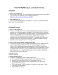
ORCA® Series 4
Clocking Overview
July 2002
Technical Note TN1015
ORCA Series 4 Clocking Features
•
•
•
•
•
•
•
•
•
•
Abundant clock routing resources
Primary, secondary, and edge clock resources
At least six edge clocks on each of the four device edges (top, bottom, left, and right).
Low skew across entire FPGA
Single-ended and differential clock inputs
Branch shut-off of primary clock for power savings
Ability to drive high fanout nets
Phase-locked loop (PLL) friendly
Cycle Boosting for increased internal and I/O performance.
Automatically routed by software
Introduction
ORCA Series 4 is a revolutionary family of high-speed FPGAs from Lattice Semiconductor Corporation. Series 4
has been designed for the delivery of networking IP with improved performance and decreased time-to-market in
mind.
To facilitate the feature-rich, high-speed architecture of Series 4, a new flexible clocking scheme has been developed.
Hardware Architecture
Figure 1. is a block diagram of the Series 4 FPGA architecture. Series 4 includes significant embedded functionality including embedded block RAMs, an integrated system bus, a microprocessor interface, and eight PLLs. Two of
the eight PLLs are dedicated for broadband applications. One targets T1/E1 rates, and one is for STS-3/STM-1
running at 155.52 MHz. The remaining six are general purpose and can operate from 20 MHz up to 420 MHz.
All clocked registers in the device are found in the following blocks: programmable logic cells (PLC), programmable
I/O cells (PICs), embedded block RAM (EBR), or system bus. Each PIC contains I/O circuitry for four programmable I/Os (PIOs).
www.latticesemi.com
1
tn1015_02
Lattice Semiconductor
ORCA Series 4 Clocking Overview
Figure 1. Series 4 FPGA Architecture Block Diagram .
EMBEDDED BLOCK RAM
CLOCK PINS
PLLs
H-SPINE
PRIMARY
CLOCK
CORE
BRANCHES
SYSTEM BUS
PFU LOGIC
HIGH-SPEED I/O
0722(F)
Clock Types
There is an abundance of clocking resources in the Series 4 FPGA/FPSC. These resources can be categorized
into three types of clocks; primary, secondary, and edge clocks. They differ based on the way the clocks are distributed across the array.
Primary Clocks
A primary clock is a globally distributed clock, of which there are eight in each Series 4 FPGA/FPSC device. A primary clock can be used for any clock in a design; however, when more than eight clocks are present, it is used for
the most heavily loaded, highest-frequency clocks. A primary clock can obtain its source from any external package pin configured as an input to the FPGA, derived from logic generated internal to the FPGA, or from any of the
PLLs. Note that there cannot be more than four primary clocks residing on the same side of the FPGA.
The primary clocks use a low-skew clock tree resource called an H-spine (refer to Figure 1). The H-spine will provide the lowest skew of the three clock types for clocks that are distributed globally across the entire FPGA array
(<400 ps skew across the largest Series 4 FPGA).
There are recommended pins to be used for primary clocks. Please refer to the package pin tables in the Series 4
data sheet for these locations (their functions are listed as PxCKxx). They are positioned in the center of each side
of the package. These pins should be used to achieve the lowest delay in reaching the H-spine routing resource.
Software will automatically select these pins if the user does not manually locate the clock pins. Also, note that a
user may select external pins for the clock other than these recommended pins and still be able to route to the Hspines; however, the path to the H-spine will be slower. If a primary clock is not placed on a primary I/O pin due to
none being available (this can happen if the user locates other signals at the primary I/O locations), a warning will
be issued by software and the primary clock will be placed on a different I/O pin. For internally generated primary
clocks, the source of these clocks is best placed close to the center of the FPGA for optimal performance. Software
will handle this automatically.
2
Lattice Semiconductor
ORCA Series 4 Clocking Overview
Differential clock inputs are supported in the Series 4 series of FPGAs. This is accomplished by the instantiation of
differential clock buffer library elements into the design. The location of these differential clock pairs is handled the
same way as for the single-ended clocks.
If a clock originates from a PLL, those clocks will be considered primary and get routed to H-spine routing
resources.
Clocks originating from the embedded ASIC block of a field-programmable system chip (FPSC) connect to the
FPGA clock routing automatically.
ispLEVER Software will assign a clock as primary if the software detects ten or more clock loads. The following is
the order of resolution by software:
• PLL and ASB clocks are assigned primary routing resources first.
• Clock signals with greater than or equal to ten component loads (1 PFU, PIO, or block RAM equals one
load) are then assigned.
If there are more than eight clocks in a design, software will select the most heavily loaded clocks for primary clock
resources after the PLL and ASB clocks have been selected. Any remaining clocks will use secondary clock routing
resources, which is explained later.
The user can alter this resolution via the preference file. The preference for this is called USE PRIMARY <net
name>. This will force the software to put the <netname> net on a primary clock resource ahead of any other
clocks. By using the USE PRIMARY preference, the order of resolution of selecting primary clocks by software is
as follows:
• User-specified primary clocks get primary resources first.
• PLL and ASB generated clocks get any remaining primary clock resources.
• Clock signals with greater than or equal to ten loads are then assigned to primary clock resources.
Secondary Clocks
Secondary clocks are used for clock and control signals. (Example: the control signals in Series 4 are LSR, CE,
and SEL.) For clocking functions that do not take up much logic (such as a function that can be contained within a
single quadrant of an FPGA, or for lower-frequency clocks when all eight primary clock resources are being used),
secondary clocking can be used. In fact, if a small module can be placed entirely within an area of the FPGA no farther than six PLCs from the edge of the array and it is clocked by an external pin, it may be desirable to use a secondary clock to save power and primary clocks without skew increases. This also allows the same clock pin to be
used as an edge clock, as will be shown later.
A secondary clock can be sourced from the same resources as a primary clock, any external pin, internally generated from a PLC, a PLL, or an ASB. In the case of an external I/O pin, there can be one unique secondary clock
coming into the Series 4 FPGA from any PIC. Note that software will issue an error message if it detects more than
one secondary clock from a single PIC (one PIC consists of four PIOs). There are no other restrictions on selecting
secondary clocks.
Care should be taken when routing secondary clocks to output buffers as there can only be two clock spines driving a PIC at one time. If the router chooses to drive a secondary clock signal to the output buffer then there are certain PIOs that the clock signal cannot drive since the clock routing resources for that particular clock signal are
used for the entire PIC. This situation occurs more often when the software tools are selecting the pinout as the
user typically keeps similar signals together alleviating this situation. If a secondary clock signal is attempted to be
routed to a spare I/O pin after the design has been placed and routed, it may be difficult to find a solution for this
clock signal.
Similarly, care should be taken when routing certain FPSC recovered clock signals. For example, the
RWCK[A:B][A:D] signals in the ORTx2G5 connect to secondary clock nets. As secondary clocks have less available resources than primary clocks, the router may have a difficult time finding a solution for all clocks depending
3
Lattice Semiconductor
ORCA Series 4 Clocking Overview
on the placement of the registers sourced by the secondary clock and the register’s relative distance from the secondary clock source. In these instances, floorplanning may be required to ensure related signals are grouped
together to facilitate a complete solution. For more details on floorplanning, see technical note TN1010, Lattice
Semiconductor Design Floorplanning.
Secondary clock routing resources reside on separate mask layers of the FPGA in order not to interfere with other
signals or clocking resources in the design. The secondary clock routes are bidirectional x 6 traces that are buffered every six PLCs apart. If a clock is contained within this six PLC area (meaning six PLCs in each direction for a
total of 12 PLCs) the clock will have very low skew. Once the clock passes through a buffer, a delay of about 400 ps
is incurred.
The ispLEVER software will identify a signal as a secondary clock by detecting six or more clock loads. The software will also use secondary clock resources for control signals that have 15 or more control type loads. Software
will automatically start assigning clocks to secondary clock resources when all eight primary clock resources are
used. The user can modify this decision with the use of the USE SECONDARY <net name> preference. With this
preference, the user can assign any clock or control signal from any source to the secondary clock routing
resources, thereby overriding software decision-making process.
Secondary Clocks and PLLs
The Series 4 PLLs were optimized to interface with the primary clock routing resources. As secondary clock routing
resources do not connect directly to the Series 4 PLLs, care must be taken when using secondary clock routing
resources with the Series 4 PLLs. One method of connecting secondary clock routing resources with the Series 4
PLLs is to use a Series 4 PFU register to divide the secondary clock in half. The output of the PFU register can
then be connected to the PLL input and multiplied by a frequency of 2. This scenario is most common with embedded ASIC block clocks that connect directly to the secondary clock routing resources. Following is an example of
this implementation:
process(RWCKBD)
begin
if RWCKBD’event and RWCKBD = ‘1’ then
clk_int <= not clk_int;
end if;
end process;
inst_pll: pllx2
port map ( clk=> clk_int, mclk=> clkx2, lock=>open );
Another method of connecting secondary clock routing resources with the Series 4 PLLs, is to route the secondary
clock to an unused bi-directional I/O to be connected to a primary clock resource. Following is an example bi-directional I/O instantiation for this application:
BMZ12F sec_clock_to_prim_clock( .I (sec_clk), .T (gnd), .O (prim_clk), .B () );
Edge Clocks
Edge clocks are clocks that reside at the perimeter of the Series 4 FPGA. Edge clocks are used for very localized
clocking of I/O elements. Because edge clocks incur significant skew (like secondary clocks), they are not suited for
clocking large busses. Although any clock in the Series 4 architecture can be used to clock the I/O flip-flops (which
reside in the PICs), an edge clock will realize the fastest clock-to-out and lowest input setup time and hold time
parameters other than with the use of the PLL resources. Note that the preferred method of getting the best I/O
performance is with the use of the PLLs that reside in the FPGA (refer to the PLL application note). The Series 4
FPGAs allow at least six different edge clocks per side of the device, as an improvement over previous FPGA architectures.
4
Lattice Semiconductor
ORCA Series 4 Clocking Overview
The source of an edge clock can be any external I/O configured as an input pin, or from a PLL. For an external I/O
pin, there can be one edge clock as an input to the FPGA per PIC. Once an edge clock is coming into a PIC, there
are rules that must be followed for selecting other PICs for edge clocks. These rules apply to edge clocks on the
same side of the Series 4 FPGAs. If a PIC is the source of an edge clock, there cannot be another PIC as a source
of an edge clock if that PIC is located a multiple of six PICs away (e.g., if PIC7 has an edge clock, then PICs 1, 13,
19, etc., cannot be used as a source for another edge clock on that side of the FPGA).
The destinations of an edge clock are PICs and a primary clock resource if that edge clock is also used as a system clock.
Edge clock routing resources reside on separate mask layers of the FPGA in order not to interfere with other signals or clocking resources in the design. The routes are the same as the secondary clock resources in that the
edge clock routes can travel six PICs (six PICs in one direction (left or up) and 5 PICs in the other direction (right or
down), plus the one PIC that the clock is coming in from, for a total of 12 PICs) with very low skew. Once the clock
goes past six PICs in a direction, it passes through a buffer, and a delay of about 400 ps is incurred.
ispLEVER software identifies an edge clock as a clock that is connected to the EC pin of an I/O flip-flop (please
refer to the ORCA Libraries Manual for pin definitions). To get the fastest clock-to-out using an edge clock, the output flip-flop should be placed in a PIC that resides within a six PIC distance of the source of this clock. In order to
get the lowest input hold times into the FPGA, an edge clock should be used with a zero hold latch (refer to ORCA
Libraries Manual and Series 4 I/O User’s Manual for details).
Interconnection of Secondary Clocks and Edge Clocks
A secondary clock at the perimeter of the device and an edge clock can be directly connected together and be
driven by the same clock pin. This allows very high-speed localized clock networks with reduced power. A single
clock pin can drive 12 PICs, one embedded block RAM, and a 12 wide by 6 deep array of PLCs. The array can be
extended in all directions through very fast programmable connections.
Edge clocks that originate from an external I/O pin do not turn corners of the FPGA. This means that if an edge
clock enters the FPGA in a PIC located less than six PICs from a corner, the edge clock resource will connect to a
reduced number of I/O registers in that direction.
Edge clocks that originate from a PLL do turn corners. They span the first six PICs that are adjacent to that corner
before getting buffered. When the source of an edge clock is a PLL, the first PICs in that corner in both directions
cannot also serve as a source of an edge clock.
Clocks as Signals
All three clock types (primary, secondary, and edge) reside on clock routing resources. As most sources of all three
clock types also connect to combinatorial logic or output buffers, in most cases, clocks signals can connect to data
routing resources as well as clock routing resources. The clock routing resource does not connect directly to data
routing resources. Consequently, as clocks originating from the embedded ASIC block of a field-programmable
system chip (FPSC) connect directly to the FPGA clock routing, care should be taken when trying to connect
embedded ASIC block originated clocks to data routing resources. One method of connecting ASIC block originated clocks to data routing resources is to route the ASIC block originated clock to an unused bi-directional I/O to
be connected to the data routing resources. Following is an example bi-directional I/O instantiation for this application:
BMZ12F asb_clock_to_data_routing( .I (asb_clk), .T (gnd), .O (out_clk), .B () );
Cycle Boosting
A feature in Series 4 FPGAs is the ability to borrow time from one register-to-register path and use that time in the
previous path before the first register. This is done with selectable clock delays for every PLC register, EBR register
and PIO register. This allows performance increases on typical critical paths from 15% to 40%. The ispLEVER
development system includes software to automatically take advantage of this capability to increase overall system
5
Lattice Semiconductor
ORCA Series 4 Clocking Overview
speed. This is done after place and route is completed and uses timing driven algorithms based on the user’s preference file. A hold time check is also performed to verify no minimum hold time issues have been introduced.
Summary
The Series 4 FPGA and FPSC devices offer a large number of clock routing resources that meet high-speed clocking needs. Although three types of clock routing are supported, the ispLEVER software suite automatically takes
care of the clock routing needs.
6