1
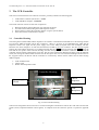
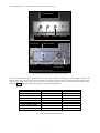
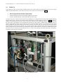
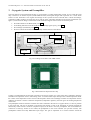
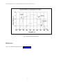
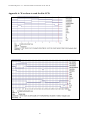
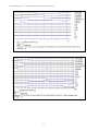
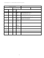
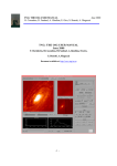
ISSN 1594-1906
Padova and Asiago Observatories
THE CCD CAMERA CONTROLLER AT THE 182 CM
D’Alessandro M., Fantinel D., Giro E.
Technical Report n. 15
August 2001
Document available at: http://www.pd.astro.it/
Vicolo dell’Osservatorio, 5 35122 Padova – Tel. +390498293411 – Fax +390418759840
This page is left intentionally blank
Technical Report N. 15 - The CCD Camera Controller at the 182 cm
1
Introduction
The CCD camera controller has been designed and built by the CCDWG (CCD Working Group) for the scientific
(Optical Imager, Low Resolution Spectrograph, High Resolution Spectrograph) and the service cameras (Guide camera,
Shack-Hartmann camera) of the Telescopio Nazionale Galileo (TNG). In the past years a complete upgrade of the
Asiago Telescope Instrumentation was planned, especially related to the CCD camera (Controller, CCD Chip,
Cryogenic Dewar and Software). In this framework the CCD camera controller designed and built for the TNG was
adopted for the AFOSC (Asiago Faint Object Spectrograph and Camera) instrument. The next sections will give an
overview of the main features of the controller and of the CCD chip. Moreover a brief description (the mechanical
arrangement) of the cryogenic system (Dewar) will be reported. The complete system mounted at the telescope is
depicted in Fig. 1.
Telescope
Preamp. Box
Afosc
Dewar
Cables
Ccd Controller
Fibre Link
Fig. 1 The AFOSC instrument, the cryogenic dewar and the CCD controller mounted at The Telescope
1
Technical Report N. 15 - The CCD Camera Controller at the 182 cm
2
The CCD Controller
This section will describe the CCD camera's electronics, primarily related to the following parts:
•
•
CCD Camera Controller (electronics) - CCDC
CCD VME Host computer - CCDVME
The CCDC controller consists of four main components:
1.
2.
3.
4.
2.1
Housing and Power Supply Board for the controller electronics
Two electronic boards (Analog board and Sequencer board)
Three Cables to connect the controller with the cryogenic system (dewar)
Fibre link with the CCDVME host computer
Controller Housing
The Analog board (named CDS) and the Sequencer are housed in a standard 19inch metallic box. The housing contains
two five-slots VME back-plane (P1/96 Pin Connectors: 3 Rows x 32 Pins) for accommodating the CDS and the
Sequencer boards. The signal and the power supply lines of the VME back-plane have been redefined and their
functions have been changed to fit with the functionalities needed by the CCD controller. The data and the signals
between the CDS and the Sequencer are exchanged through this bus. Fig. 2 shows the housing while Fig. 3 shows the
front and the rear panels of the controller housing. Onto the front panel are located the connectors used to bond the
controller with the Dewar containing the CCD chip. The rear panel contains the Main Power Supply plug, the ON/OFF
switch, the cooling fan and the SMA connectors for the fibre optic link. The CCD controller housing is located close to
the cryogenic Dewar; the Dewar and the controller are connected by means of three cables each of them carrying
different signals:
•
•
•
Video and Bias Cable
Clocks Cable
Shutter and Temperature Cable
Controller Housing
CDS &
Sequencer
Power supply
Board
VME
Backplanes
Fig. 2 CCD Controller Housing
This kind of arrangement has been chosen to avoid electromagnetic interferences between the video lines and the other
signals (clocks, temperature/shutter control signals). A complete list of the connectors pin-out is reported in Appendix
B.
2
Technical Report N. 15 - The CCD Camera Controller at the 182 cm
Front panel
Clocks Vid/Bias
On/Off Sw
Main PS
Temp Connectors
Rear panel
Cooling Fan
Fiber Optic Link
Connectors
Fig. 3 CCD Controller Housing, front and rear panels
Inside the controller housing are located the power supply board (PSB), the transformer and the bridge rectifiers. The
PSB provides all the voltages and currents needed to operate the CCD controller in a quad readout configuration (four
outputs of one CCD or four CCDs with one output). All voltage supplies are linear and optimized for efficiency and
reliability. Tab. 1 summarizes the main parameters of the power supply board.
Voltages
Analog +/-20V
Analog +/-8V
Analog +30V
Digital +5V
Temperature +/-12V
Temperature +24V
Analog GND (AGND)
Digital GND (DGND)
Temp. GND (TGND)
Default Setting
+/-20V
+/-8V
+32V
+5.1V
+/-12V
+24.5V
Tab. 1 Power Supply Board Parameters
3
Max Current
1.0Amp
1.0 Amp
0.5 Amp
3.5 Amp
0.5 Amp
0.5 Amp
Technical Report N. 15 - The CCD Camera Controller at the 182 cm
2.2
Sequencer
The Sequencer board is a double eurocard form factors (6U size B, 160 X 234 mm). The board acts as motherboard for
four standard TRAM service slots, two of them are used to mount, permanently, two piggy-back modules: the DTM560
and the SMT227 boards, the other two slots are for service purposes. The DTM560 module is the heart of the Sequencer
and it was purchased from Perimos, Germany. It is a standard TRAM module, which contains two high-speed
processors: a 16-bit T222 20 MHz transputer and a 24-bit 56001 MOTOROLA DSP (20MHz). The transputer and DSP
communicate by means of a shared memory. The SMT227, from Sundance (or PST207 TRAM module from Paratech),
is a standard TRAM fibre optic link module, which provides the link between the CCD controller and the CCDVME
host computer. Besides these two commercial parts, the Sequencer contains all the electronic circuits needed to support
functions that are not directly involved with the readout of the CCD chip such as: temperature control and setting,
shutter (curtain or iris) control, external synchronization circuit and address decoder circuits for the Motorola DSP. The
functions of the Transputer are: data, commands and telemetry handling, bias and clock voltages programming and
communication with the host computer (via fibre optic link). The Motorola DSP (20MHz 56001 DSP) is used as timing
generator to read the CCD chip and to control the auxiliary functions related to the CCD operations (exposure time,
shutter and temperature). The list below summarizes the main features of the Sequencer board:
•
•
•
•
•
•
2.3
16 Digital outputs for pixel processing, i.e. CCD serial clocks, clamp, hold, start conv. etc
12 Digital outputs for CCD parallel clocks and line clamp
Software programmable Temperature control (D/A and A/D converters)
Shutter control (Iris and Curtain shutters)
Sequencer built around Motorola DSP56000/1 (Time resolution 100nanosecs)
Data handling and commands interface by means of Transputer T222
Analog Electronics CDS
The CDS (Correlated Double Sampling) board is a double eurocard form factors (6U size B, 160 X 234 mm) like the
Sequencer. The function of this board is to sample, to filter and to convert each pixel of the CCD chip. The main parts
of the analog processing circuit are: the differential input amplifier, the integrator amplifier (integrate, hold and reset)
and the Analog to Digital Converter (16 Bit resolution). The A/D converter is also used for the telemetry. In addition
the generation of the Mos level for the CCD clock and the bias voltages are located inside this board (8/12 Bit
resolution). The main features of the CDS are the following:
•
•
•
•
•
•
x differential video channels with correlated double sampling (CDS)
x 16 bits resolution ADCs (Crystal CS5101), used for Data and Telemetry
x 18 bits resolution DACs for video channel off-set
8 Software programmable bias voltages with 12 Bits resolution
8 Buffered Serial clocks with software programmable low and high levels with 8 Bits resolution
8 Buffered Parallel clocks with software programmable low and high levels with 8 Bits resolution
The DC bias and the clock (high and low) voltage ranges are shown in Tab. 2.
DC Bias Voltage
Bias 1
Bias 2
Bias 3
Bias 4
Bias5--Bias8
Function
Reset Drain of CCD
General Use
General Use
Output Drain of CCD
Last Gate, Output Gate, Substrate of CCD
(or general use)
Range (Volts)
+9/+21
+9/+21
+9/+21
+19/+30
-12/+12
Serial Clocks
Parallel clocks
-10/+10
-10/+10
DC Clock Voltage
Clk1--Clk8
Clk9--clk16
Tab. 2 Voltage ranges
4
Technical Report N. 15 - The CCD Camera Controller at the 182 cm
2.4
VMEACQ
The VMEACQ system is built around a standard 19inch rack, which contains the VME back-plane, the power supply
module and the hard disk drive. The boards involved to CCD control are the following (see Fig. 4):
•
•
•
•
CPU Eurocom-6 (Master) from Eltec Gmbh Germany
TCD 101 Graphic boards from Eltec Gmbh Germany
ATX290 Transputer Interface board VME-VSB from Atenix Italy
ATX630 32 Mbyte Memory board VME-VSB from Atenix Italy;
The CPU Eurocom-6 controls all the functions of the VMEACQ. It is equipped with a real-time multi-tasking Operating
System (PDOS) and a software environment (GATE) developed by the TNG Software Group, see Ref. 1. GATE is a
modular environment that provides the overall control of the functions of the VMEACQ and of the communication with
the other VME or Workstations. The communication between the CPU and the ATX290 board is done by means of
Dual Port Ram (DPR) contained into the Atx290, all the commands and the telemetry are exchanged using this shared
memory(VME Bus). The Data coming from the CCD controller, via the fibre link, are stored by the ATX 290 onto the
ATX630 memory board using the VSB bus. The TCD101 graphic board is dedicated to the "Real Time" display of the
image coming from the CCD controller (8 bit depth-256 colours). Other boards are inserted in the VMEACQ rack and
are used for service operations of the telescope such as: control of the telescope movements during the "auto-guide",
acquisition of the telescope coordinates.
Fig. 4 The VMEACQ system
5
Technical Report N. 15 - The CCD Camera Controller at the 182 cm
3
Cryogenic System and Preamplifier
The CCD must be cooled (thermoelectrically or cryogenically) to reduce thermal dark current. In our system the CCD
chip is housed in an Oxford cryostat (model MN1815 INV) with liquid nitrogen tank capacities of 1.5 litres which
assures 12 hour hold times. The original front flange of this cryostat has been removed and a custom front flange,
containing a UBK7 window, has been built to fit with the Afosc instrument mechanical and optical requirements (see
figure 5). Onto this front flange is mounted the CCD mechanical support which consists of four main parts:
•
•
•
•
the CCD Printed Circuit Board (PCB, see Fig. 6)
an insulating material to hold the PCB and the cold finger (glass epoxy), see Fig. 7a
the cold finger (aluminium), see Fig. 7b
the wires to/from the PCB and the hermetically sealed connector of the Dewar
Dewar side
UBK7 window
Focal plane
Afosc side
Fig. 5 Front flange of the dewar with UBK window
Fig. 6 The PCB CCD chip for the Site chip
Cooling is transferred from the nitrogen cold plate to the chip by means of a copper strap that is adjusted in length to
hold the CCD temperature close to the working value. A resistive heater keeps the chip to the wanted temperature under
the control of the temperature control circuit of the Sequencer board. The cold finger contains two temperature sensors
(AD590), the former is used to control the temperature (temperature regulator), the latter gives the working temperature
of the CCD.
The preamplifier board is housed in a metallic box that is attached to the side of a cryogenic dewar, as close as possible
to the CCD chip. The box is mounted on the dewar and contains a hole in the base-plate for passing through the
hermetically sealed circular connector (Amphenol 55pin) of the dewar. Onto the preamplifier box are mounted two
connectors to bond (by means of two cables) the preamplifier to the CCD controller (see previous section). The
preamplifier contains four fully differential input stages. The gain is adjustable via a resistors network. Inside the
6
Technical Report N. 15 - The CCD Camera Controller at the 182 cm
preamplifier board there are, also, the buffers to boost the bias voltages needed by the CCD and the generation of the
local power supply from three main voltages (+32V, +/-20V).
Site 1k x 1k CCD
a
CCD Support structure (CCD side)
Cold finger
b
CCD Pcb
Heater resistor
CCD Support structure (bottom)
Fig. 7a, 7b Support structure for the CCD
4
CCD Chip
The CCD chip currently mounted at the AFOSC instrument is an SI-003AB from Site Inc USA (Thinned Back
Illuminated MPP, Serial number 7405GBR05-A1 VisAR-Coat). The device specifications are the following:
Format
Pixel Size
Imaging Area
Dark Current @-15C°
Readout Noise
Full Well
Output gain ( Amp B)
Parallel CTE ( Amp B)
Serial CTE ( Amp B)
1024 * 1024 pixels
24 µm * 24 µm
24.6 mm * 24.6 mm
28 e-/pixel/sec (MPP)
~5 e- RMS
350K e1.2 µV/ e0.999999
0.999996
The chip has four outputs that are located in each corner of the device at the ends of the serial registers. Fig. 8 presents a
schematic view of the CCD chip configuration. The Si-003A chip can be operated with one, two, three or four outputs
simultaneously. In our case we use only the B output amplifier. The time required to read the full image, from one
amplifier, is about
7
Technical Report N. 15 - The CCD Camera Controller at the 182 cm
Fig. 8 SI-003A functional diagram
50 seconds (40µsec per pixel and 100µsec per line), if we need to read images at higher rate, it is possible to define a
small area of the chip centred on the reference object, for example with a sub-area (window) of 128 by 128 pixels the
readout time goes down to 1sec. This way of reading the chip gives the optimal combination of a relatively fast frame
rate while allowing long pixel time (inside the sub-area) to minimize the read-out noise (Correlated Double Sampling
technique for each pixel). The working bias and clock voltages are reported in Tab. 3. The chip is liquid Nitrogen
cooled at about -100°C, as described in the previous section. The Site SI-003A is thinned back illuminated CCD with
VisAr coating, that provides superior quantum efficiency as reported in Fig. 9. In Appendix A are reported the
waveforms used to read the chip.
CCD Name - CDS Name
VDD - OUT4
VOD - OUT1
VOG-OUT6
VSUB-AGND
VOS(a,b,c,d)-VIDX(1,2,3,4)
CCD Name-Seq.CDS Name
S2ad-Clk1
S2bc-Clk2
S3ad-Clk3
S3bc-Clk4
S1abcd-Clk5
SWabcd-Clk6
RGabcd-Clk7
P1Uab-Clk9
P2Uab-Clk10
P3Uabcd-Clk11
TGULabcd-Clk12
P1Lcd-Clk13
P2Lcd-Clk15
Bias Voltages
Function
Output Drain Voltage
Reset Drain Voltage
Output Gate Voltage
Substrate Voltage
Video output line
Clocks Voltages
Function
Serial Clock 2 Amp a&d
Serial Clock 2 Amp b&c
Serial Clock 3 Amp b&c
Serial Clock 3 Amp b&c
Serial Clock 1 Amp a&b&c&d
Summing well Amp a&b&c&d
Reset Gate Amp a&b&c&d
Parallel 1 Clock Amp a&b
Parallel 2 Clock Amp a&b
Parallel 3 Clock Amp a&b&c&d
Transfer Gate Clock Amp a&b&c&d
Parallel 1 Clock Amp c&d
Parallel 2 Clock Amp c&d
Tab. 3 Site SI-003A CCD working parameters
8
Voltages (V)
24.7
15.7
-3.9
AGND
20KΩ(Load)
High Level (V)
-4.0
-4.0
-4.0
-4.0
-4.0
-4.0
0.0
-9.0
-9.0
-9.0
-9.0
-9.0
-9.0
Low Level (V)
+8.0
+8.0
+8.0
+8.0
+8.0
+8.0
+12.0
+4.0
+4.0
+7.0
+7.0
+4.0
+4.0
Technical Report N. 15 - The CCD Camera Controller at the 182 cm
Fig. 9 SI-003A Quantum Efficiency
References
Ref. 1 User Manuals, September 1999. Gate User Manual
9
Technical Report N. 15 - The CCD Camera Controller at the 182 cm
Appendix A: Waveform to read the Site CCD
10
Technical Report N. 15 - The CCD Camera Controller at the 182 cm
11
Technical Report N. 15 - The CCD Camera Controller at the 182 cm
12
Technical Report N. 15 - The CCD Camera Controller at the 182 cm
Appendix b: Crio Site 1K x 1K cabling
Instrument :
Crio Site 1K x 1K Afosc
Controller-J1 connector
Connector Type 1:
62GB-56T-16-26 S
Contr-J1
Amphenol
Clocks
55 pin Cryo
conn
Pin
Pin
CCD PCB
Function
A
b
Clock 1 A
S2ad
B
a
Clock 2 A
S2bc
C
RTN 1
D
F
Clock 3 A
S3ad
E
Z
Clock 4 A
S3bc
F
E
Clock 5 A
S1abcd
G
D
Swabcd Clock 6 A
H
RTN 2
J
Y
RGabcd Clock 7 A
K
Clock 8 A
L
DD
Clock 9 A
P1Uab
M
CC
Clock 10 A
P2Uab
N
RTN 3
P
H
P3Uabcd Clock 11 A
R
c
TGULabcd Clock 12 A
S
T
U
V
W
X
Y
Z
a
b
c
s
P1Lbc
t
P2Lbc
Clock 13 A
Common
Shield
RTN 4
RTN 5
RTN 6
Clock 16 A
Clock 15 A
RTN 7
Clock 14 A
Spare
Spare
13
Comment
Serial clocks 2 a&d amplifiers (-4V/+9V)
Serial clocks 2 b&c amplifiers (-4V/+9V)
Sheet 1 of 1
Serial clocks 3 a&d amplifiers (-4V/+9V)
Serial clocks 3 b&c amplifiers (-4V/+9V)
Serial clocks 1 a&b&c&d amplifiers (-4V/+9V)
Summing Well clocks a&b&c&d amplifiers (-4V/+9.6V)
Reset Gate clocks a&b&c&d amplifiers (0V/+12V)
Parallel clock 1 Upper Quadrant (-9.0V/+4.0V)
Parallel clock 2 Upper Quadrant (-9.0V/+4.0V)
Parallel clock 3 Common Upper&Lower Quadrants(-9.0V/+4.0V)
Transfer Gate clock Common Upper&lower Quadrants (9.0V/+7V)
Parallel clock 1 Lower Quadrant (-9.0V/+4.0V)
Parallel clock 2 Lower Quadrant (-9.0V/+4.0V)
Technical Report N. 15 - The CCD Camera Controller at the 182 cm
Instrument :
Crio Site 1K x 1K Afosc
Controller-J2 connector Connector Type 1:
62GB-56T-16-32 S
Contr-J2
Amphenol
VidBias
55 pin
Cryo conn
Pin
Pin
CCD PCB
Function
A
i
VRDa,b,c,d Bias 1
B
Bias 2
C
Bias 3
D
j
VDDa,b,c,d Bias 4
E
Bias 5
F
h
VLGa,b,c,d Bias 6
G
B
Video 1 - pos.
OUTa
H
A
Video 1 - neg.
VDDa
J
W
Video 2 - pos.
OUTb
K
V
Video 2 - neg.
VDDb
L
Comm.Video
Shield
M
p
Video 3 - pos.
OUTc
N
n
Video 3 - neg.
VDDc
P
U
Video 4 - pos.
OUTd
R
T
Video 4 - neg.
VDDd
S
+20V
T
-20V
U
Comm.Bias
Shield
V
A_GND
W
Bias 8
X
Bias 7
Y
AA
A_GND
GND
Z
AA
A_GND
GND
a
+30V
b
+30V_RET
c
LineClamp
d
GAIN
e
±20V RET
f
Spare
g
Spare
h
Spare
i
Spare
14
Comment
Reset Drain Voltage
+15.7 Volts
Out Drain voltage
+25.5Volts
Las Gate Voltage
-3.9Volts
Twisted pairs CCD Output A (20KΩ load)
Twisted pairs
Twisted pairs CCD Output B (20KΩ load)
Twisted pairs
Twisted pairs
Twisted pairs
Twisted pairs
Twisted pairs
CCD Output C (20KΩ load)
CCD Output D (20KΩ load)
Sheet 1 of 1
Technical Report N. 15 - The CCD Camera Controller at the 182 cm
Instrument :
Crio Site 1K x 1K Afosc
Controller-J3 connector Connector Type 1:
62GB-56T-16-26 S
Contr-J3
Oxford
Temperatures
Cryo
Connector
Pin
Pin
Function
A
C
TMP 1
B
B
TMP 2
C
D
TMP 3
D
TMP 4
E
TMP 5
F
A
TMP 6
G
H
+5V REF
H
K
Heather 1
J
L
Heather 2
K
ENACLK
L
DISCLK
M
SHUTTER 1
OUT
N
SHUTTER 2
OUT
P
SHUT A
R
SHUT B
S
V SHUT
T
Peltier pos.
U
Peltier neg.
V
TGND
W
X
Y
Z
a
b
c
15
Comment
CCD Temperature Sensor (S3)
Crio Wall Temperature Sensor (S2)
LN2 Temperature Sensor (S4)
CCD Temperature Control Sensor (S1)
Common Voltage for Temperature Sensors
Temperature Control Resistor
Temperature Control Resistor
Temperature ground
Sheet 1 of 1
Technical Report N. 15 - The CCD Camera Controller at the 182 cm
A = Sensor S1 regulator
B = Sensor S2 Crio Wall Temperature
C = Sensor S3 CCD Temp
C
D = Sensor S4 LN2 Temperature
B
D
F
E = N.C.
A
E
J
F = N.C.
H
H = Sensors 1 2 3 4 V Common
L
K
K = Heater Resistor
J = N.C.
L = Heater Resistor
Oxford Temperatures Connector (Site 1k x 1k)
16